

TelCom Semiconductor Inc TC4469MJD, TC4467EJD, TC4467CPD, TC4467COE, TC4468COE Datasheet
...
4-261
TELCOM SEMICONDUCTOR, INC.
7
6
5
4
3
1
2
8
LOGIC-INPUT CMOS QUAD DRIVERS
FEATURES
■ High Peak Output Current ............................... 1.2A
■ Wide Operating Range ............................ 4.5 to 18V
■ Symmetrical Rise and Fall Times................25nsec
■ Short, Equal Delay Times ............................75nsec
■ Latchproof! Withstands 500mA Inductive Kickback
■ 3 Input Logic Choices
— AND / NAND / AND + Inv
■ 2kV ESD Protection on All Pins
APPLICATIONS
■ General-Purpose CMOS Logic Buffer
■ Driving All Four MOSFETs in an H-Bridge
■ Direct Small Motor Driver
■ Relay or Peripheral Drivers
■ CCD Driver
■ Pin-Switching Network Driver
ORDERING INFORMATION
Part No. Package Temp. Range
TC446xCOE 16-Pin SOIC (Wide) 0° to +70°C
TC446xCPD 14-Pin Plastic DIP 0° to +70°C
TC446xEJD 14-Pin CerDIP – 40° to +85°C
TC446xMJD 14-Pin CerDIP – 55° to +125°C
GENERAL DESCRIPTION
The TC446X family of four-output CMOS buffer/drivers
are an expansion from our earlier single- and dual-output
drivers. Each driver has been equipped with a two-input
logic gate for added flexibility.
The TC446X drivers can source up to 250 mA into loads
referenced to ground. Heavily loaded clock lines, coaxial
cables, and piezoelectric transducers can all be easily
driven with the 446X series drivers. The only limitation on
loading is that total power dissipation in the IC must be kept
within the power dissipation limits of the package.
The TC446X series will not latch under any conditions
within their power and voltage ratings. They are not subject
to damage when up to 5V of noise spiking (either polarity)
occurs on the ground line. They can accept up to half an amp
of inductive kickback current (either polarity) into their outputs without damage or logic upset. In addition, all terminals
are protected against ESD to at least 2000V.
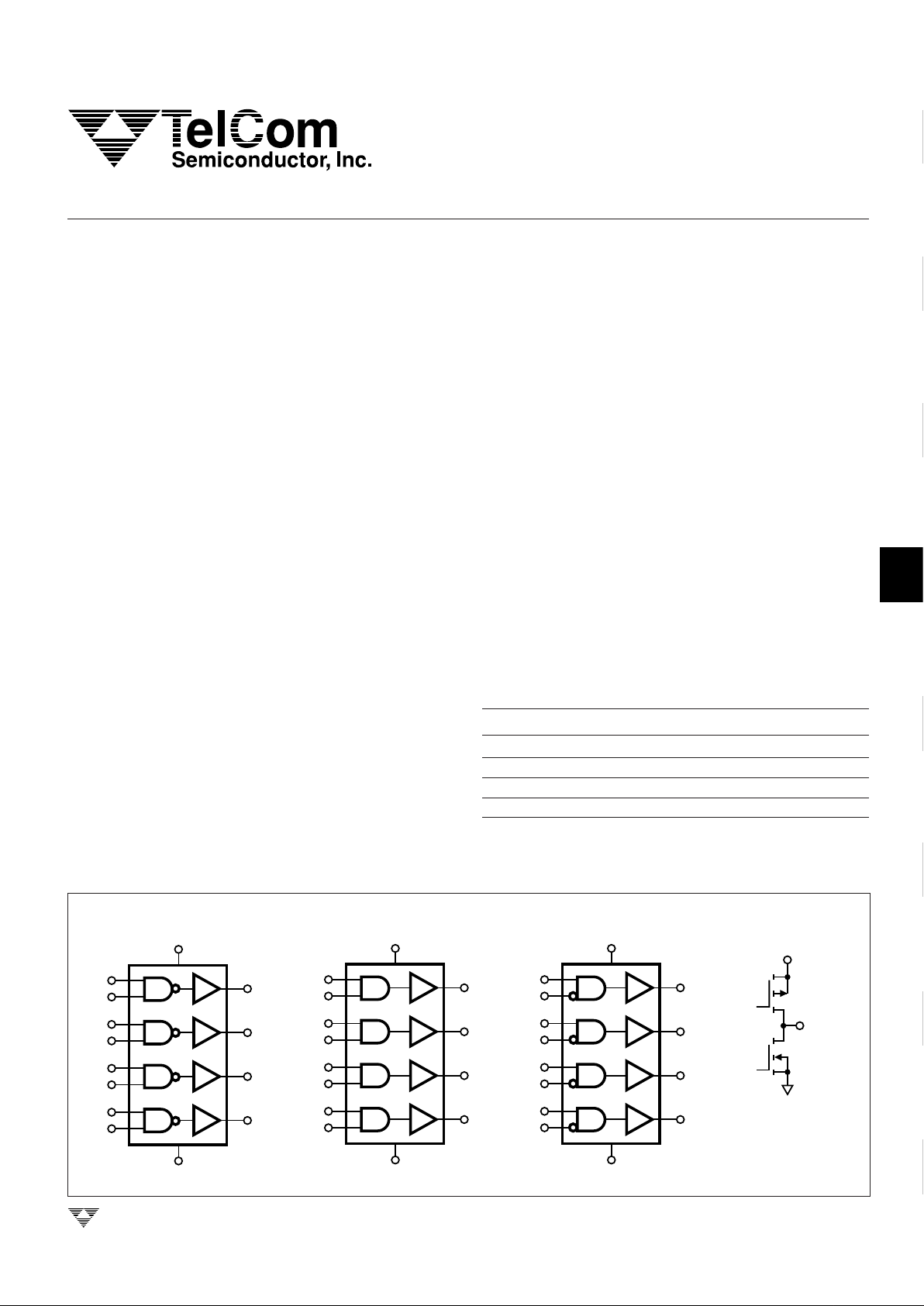
TC4467
TC4468
TC4469
x indicates a digit must be added in this position to define the device
input configuration: TC446x — 7 NAND
8 AND
9 AND with INV
LOGIC DIAGRAMS
TC4468
TC4467
OUTPUT
TC446X
V
DD
V
DD
14
7
1Y
13
1
2
1B
1A
2Y
12
3
4
2B
2A
3Y
11
5
6
3B
3A
4Y
10
8
9
4B
4A
GND
TC4469
V
DD
14
7
1Y
13
1
2
1B
1A
2Y
12
3
4
2B
2A
3Y
11
5
6
3B
3A
4Y
10
8
9
4B
4A
GND
V
DD
14
7
1Y
13
1
2
1B
1A
2Y
12
3
4
2B
2A
3Y
11
5
6
3B
3A
4Y
10
8
9
4B
4A
GND
TC4467/8/9-6 10/21/96
4-262
TELCOM SEMICONDUCTOR, INC.
LOGIC-INPUT CMOS
QUAD DRIVERS
TC4467
TC4468
TC4469
Package Thermal Resistance
14-Pin CerDIP R
θJ-A
...................................... 100°C/W
R
θJ-C
......................................... 23°C/W
14-Pin Plastic DIP R
θJ-A
......................................... 80°C/W
R
θJ-C
......................................... 35°C/W
16-Pin Wide SOIC R
θJ-A
......................................... 95°C/W
R
θJ-C
......................................... 28°C/W
*Static-sensitive device. Unused devices must be stored in conductive
material. Protect devices from static discharge and static fields. Stresses
above those listed under Absolute Maximum Ratings may cause permanent damage to the device. These are stress ratings only and functional
operation of the device at these or any other conditions above those
indicated in the operational sections of the specifications is not implied.
Exposure to Absolute Maximum Rating Conditions for extended periods
may affect device reliability.
Symbol Parameter Test Conditions Min Typ Max Unit
Input
V
IH
Logic 1, High Input Voltage Note 3 2.4 — V
DD
V
V
IL
Logic 0, Low Input Voltage Note 3 0 — 0.8 V
I
IN
Input Current 0V ≤ VIN ≤ V
DD
– 1 — 1 µA
Output
V
OH
High Output Voltage I
LOAD
= 100µA (Note 1) VDD – 0.025 — — V
V
OL
Low Output Voltage I
LOAD
= 10mA (Note 1) — — 0.15 V
R
O
Output Resistance I
OUT
= 10mA, VDD = 18V — 10 15 Ω
I
PK
Peak Output Current — 1.2 — A
I
DC
Continuous Output Current Single Output — — 300 mA
Total Package 500
I Latch-Up Protection 4.5V ≤ V
DD
≤ 16V 500 — — mA
Withstand Reverse Current
Switching Time
t
R
Rise Time Figure 1 — 15 25 nsec
t
F
Fall Time Figure 1 — 15 25 nsec
t
D1
Delay Time Figure 1 — 40 75 nsec
t
D2
Delay Time Figure 1 — 40 75 nsec
Power Supply
I
S
Power Supply Current — 1.5 4 mA
V
DD
Power Supply Voltage Note 2 4.5 — 18 V
ELECTRICAL CHARACTERISTICS:
Measured at TA = +25°C with 4.5V ≤ VDD ≤ 18V, unless otherwise specified.
TRUTH TABLE
Part No. TC4467 NAND TC4468 AND TC4469 AND/INV
INPUTS A H HL L HHLL HHLL
INPUTS B H LH L HLHL HLHL
OUTPUTS TC446X LHHH HLLL LHLL
H = High L = Low
ABSOLUTE MAXIMUM RATINGS*
Supply Voltage ......................................................... +20V
Input Voltage .........................(GND – 5V) to (VDD + 0.3V)
Maximum Chip Temperature
Operating........................................................ +150°C
Storage ............................................. – 65° to +150°C
Maximum Lead Temperature
(Soldering, 10 sec) .........................................+300°C
Operating Ambient Temperature Range
C Device .................................................. 0° to +70°C
E Device ............................................. – 40° to +85°C
M Device........................................... – 55° to +125°C
Package Power Dissipation (TA ≤ 70°C)
14-Pin CerDIP ................................................840mW
14-Pin Plastic DIP...........................................800mW
16-Pin Wide SOIC ..........................................760mW
4-263
TELCOM SEMICONDUCTOR, INC.
7
6
5
4
3
1
2
8
LOGIC-INPUT CMOS
QUAD DRIVERS
TC4467
TC4468
TC4469
Symbol Parameter Test Conditions Min Typ Max Unit
Input
V
IH
Logic 1, High Input Voltage (Note 3) 2.4 — — V
V
IL
Logic 0, Low Input Voltage (Note 3) — — 0.8 V
I
IN
Input Current 0V ≤ VIN ≤ V
DD
– 10 — 10 µA
Output
V
OH
High Output Voltage I
LOAD
= 100 µA (Note 1) V
DD
– 0.025 — — V
V
OL
Low Output Voltage I
LOAD
= 10 mA (Note 1) — — 0.30 V
R
O
Output Resistance I
OUT
= 10 mA, VDD = 18V — 20 30 Ω
I
PK
Peak Output Current — 1.2 — A
I Latch-Up Protection 4.5V ≤ VDD ≤ 16V 500 — — mA
Withstand Reverse Current
Switching Time
t
R
Rise Time Figure 1 — — 50 nsec
t
F
Fall Time Figure 1 — — 50 nsec
t
D1
Delay Time Figure 1 — — 100 nsec
t
D2
Delay Time Figure 1 — — 100 nsec
Power Supply
I
S
Power Supply Current — — 8 mA
I
S
Power Supply Voltage Note 2 4.5 — 18 V
ELECTRICAL CHARACTERISTICS: Measured throughout operating temperature range with 4.5V ≤ V
DD
≤ 18V,
unless otherwise specified.
NOTES: 1. Totem-pole outputs should not be paralleled because the propagation delay differences from one to the other could cause one driver to
drive high a few nanoseconds before another. The resulting current spike, although short, may decrease the life of the device.
2. When driving all four outputs simultaneously in the same direction, VDD shall be limited to 16V. This reduces the chance that internal
dv/dt will cause high-power dissipation in the device.
3. The input threshold has about 50 mV of hysteresis centered at approximately 1.5V. Slow moving inputs will force the device to
dissipate high peak currents as the input transitions through this band. Input rise times should be kept below 5 µs to avoid high internal
peak currents during input transitions. Static input levels should also be maintained above the maximum or below the minimum input
levels specified in the "Electrical Characteristics" to avoid increased power dissipation in the device.
PIN CONFIGURATIONS
1
2
3
4
5
6
7
14
13
12
11
10
9
8
1A
1B
2A
2B
3A
3B
GND
V
1Y
2Y
3Y
4Y
4B
4A
DD
1
2
3
4
5
6
7
8
16
13
12
11
10
9
1A
1B
2A
2B
3A
3B
GND
GND
V
1Y
2Y
3Y
4Y
4B
4A
DD
V
DD
15
14
TC4467/8/9
TC4467/8/9
16-Pin SOIC (Wide) 14-Pin Plastic DIP/CerDIP
 Loading...