

Datasheet TC4469MJD, TC4467EJD, TC4467CPD, TC4467COE, TC4468COE Datasheet (TelCom Semiconductor)
...
4-261
TELCOM SEMICONDUCTOR, INC.
7
6
5
4
3
1
2
8
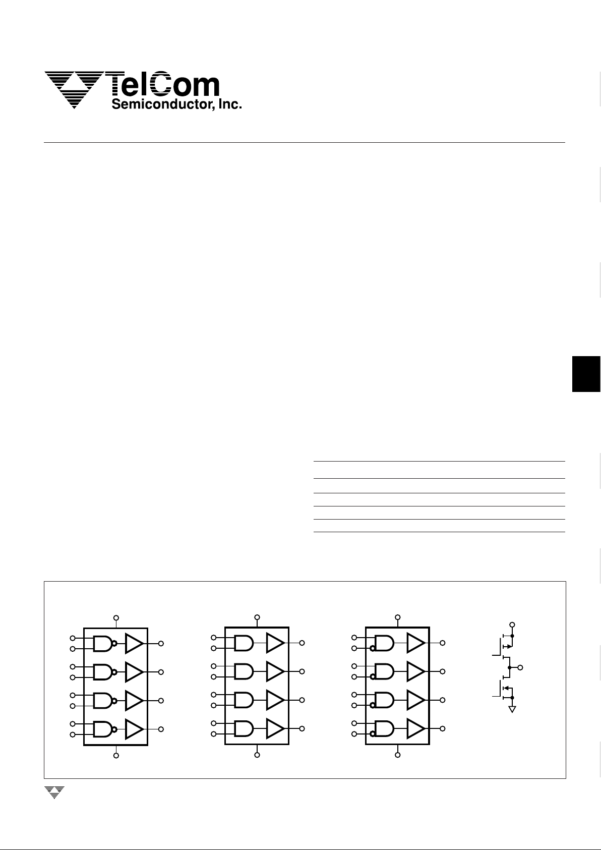
LOGIC-INPUT CMOS QUAD DRIVERS
FEATURES
■ High Peak Output Current ............................... 1.2A
■ Wide Operating Range ............................ 4.5 to 18V
■ Symmetrical Rise and Fall Times................25nsec
■ Short, Equal Delay Times ............................75nsec
■ Latchproof! Withstands 500mA Inductive Kickback
■ 3 Input Logic Choices
— AND / NAND / AND + Inv
■ 2kV ESD Protection on All Pins
APPLICATIONS
■ General-Purpose CMOS Logic Buffer
■ Driving All Four MOSFETs in an H-Bridge
■ Direct Small Motor Driver
■ Relay or Peripheral Drivers
■ CCD Driver
■ Pin-Switching Network Driver
ORDERING INFORMATION
Part No. Package Temp. Range
TC446xCOE 16-Pin SOIC (Wide) 0° to +70°C
TC446xCPD 14-Pin Plastic DIP 0° to +70°C
TC446xEJD 14-Pin CerDIP – 40° to +85°C
TC446xMJD 14-Pin CerDIP – 55° to +125°C
GENERAL DESCRIPTION
The TC446X family of four-output CMOS buffer/drivers
are an expansion from our earlier single- and dual-output
drivers. Each driver has been equipped with a two-input
logic gate for added flexibility.
The TC446X drivers can source up to 250 mA into loads
referenced to ground. Heavily loaded clock lines, coaxial
cables, and piezoelectric transducers can all be easily
driven with the 446X series drivers. The only limitation on
loading is that total power dissipation in the IC must be kept
within the power dissipation limits of the package.
The TC446X series will not latch under any conditions
within their power and voltage ratings. They are not subject
to damage when up to 5V of noise spiking (either polarity)
occurs on the ground line. They can accept up to half an amp
of inductive kickback current (either polarity) into their outputs without damage or logic upset. In addition, all terminals
are protected against ESD to at least 2000V.
TC4467
TC4468
TC4469
x indicates a digit must be added in this position to define the device
input configuration: TC446x — 7 NAND
8 AND
9 AND with INV
LOGIC DIAGRAMS
TC4468
TC4467
OUTPUT
TC446X
V
DD
V
DD
14
7
1Y
13
1
2
1B
1A
2Y
12
3
4
2B
2A
3Y
11
5
6
3B
3A
4Y
10
8
9
4B
4A
GND
TC4469
V
DD
14
7
1Y
13
1
2
1B
1A
2Y
12
3
4
2B
2A
3Y
11
5
6
3B
3A
4Y
10
8
9
4B
4A
GND
V
DD
14
7
1Y
13
1
2
1B
1A
2Y
12
3
4
2B
2A
3Y
11
5
6
3B
3A
4Y
10
8
9
4B
4A
GND
TC4467/8/9-6 10/21/96
4-262
TELCOM SEMICONDUCTOR, INC.
LOGIC-INPUT CMOS
QUAD DRIVERS
TC4467
TC4468
TC4469
Package Thermal Resistance
14-Pin CerDIP R
θJ-A
...................................... 100°C/W
R
θJ-C
......................................... 23°C/W
14-Pin Plastic DIP R
θJ-A
......................................... 80°C/W
R
θJ-C
......................................... 35°C/W
16-Pin Wide SOIC R
θJ-A
......................................... 95°C/W
R
θJ-C
......................................... 28°C/W
*Static-sensitive device. Unused devices must be stored in conductive
material. Protect devices from static discharge and static fields. Stresses
above those listed under Absolute Maximum Ratings may cause permanent damage to the device. These are stress ratings only and functional
operation of the device at these or any other conditions above those
indicated in the operational sections of the specifications is not implied.
Exposure to Absolute Maximum Rating Conditions for extended periods
may affect device reliability.
Symbol Parameter Test Conditions Min Typ Max Unit
Input
V
IH
Logic 1, High Input Voltage Note 3 2.4 — V
DD
V
V
IL
Logic 0, Low Input Voltage Note 3 0 — 0.8 V
I
IN
Input Current 0V ≤ VIN ≤ V
DD
– 1 — 1 µA
Output
V
OH
High Output Voltage I
LOAD
= 100µA (Note 1) VDD – 0.025 — — V
V
OL
Low Output Voltage I
LOAD
= 10mA (Note 1) — — 0.15 V
R
O
Output Resistance I
OUT
= 10mA, VDD = 18V — 10 15 Ω
I
PK
Peak Output Current — 1.2 — A
I
DC
Continuous Output Current Single Output — — 300 mA
Total Package 500
I Latch-Up Protection 4.5V ≤ V
DD
≤ 16V 500 — — mA
Withstand Reverse Current
Switching Time
t
R
Rise Time Figure 1 — 15 25 nsec
t
F
Fall Time Figure 1 — 15 25 nsec
t
D1
Delay Time Figure 1 — 40 75 nsec
t
D2
Delay Time Figure 1 — 40 75 nsec
Power Supply
I
S
Power Supply Current — 1.5 4 mA
V
DD
Power Supply Voltage Note 2 4.5 — 18 V
ELECTRICAL CHARACTERISTICS:
Measured at TA = +25°C with 4.5V ≤ VDD ≤ 18V, unless otherwise specified.
TRUTH TABLE
Part No. TC4467 NAND TC4468 AND TC4469 AND/INV
INPUTS A H HL L HHLL HHLL
INPUTS B H LH L HLHL HLHL
OUTPUTS TC446X LHHH HLLL LHLL
H = High L = Low
ABSOLUTE MAXIMUM RATINGS*
Supply Voltage ......................................................... +20V
Input Voltage .........................(GND – 5V) to (VDD + 0.3V)
Maximum Chip Temperature
Operating........................................................ +150°C
Storage ............................................. – 65° to +150°C
Maximum Lead Temperature
(Soldering, 10 sec) .........................................+300°C
Operating Ambient Temperature Range
C Device .................................................. 0° to +70°C
E Device ............................................. – 40° to +85°C
M Device........................................... – 55° to +125°C
Package Power Dissipation (TA ≤ 70°C)
14-Pin CerDIP ................................................840mW
14-Pin Plastic DIP...........................................800mW
16-Pin Wide SOIC ..........................................760mW
4-263
TELCOM SEMICONDUCTOR, INC.
7
6
5
4
3
1
2
8
LOGIC-INPUT CMOS
QUAD DRIVERS
TC4467
TC4468
TC4469
Symbol Parameter Test Conditions Min Typ Max Unit
Input
V
IH
Logic 1, High Input Voltage (Note 3) 2.4 — — V
V
IL
Logic 0, Low Input Voltage (Note 3) — — 0.8 V
I
IN
Input Current 0V ≤ VIN ≤ V
DD
– 10 — 10 µA
Output
V
OH
High Output Voltage I
LOAD
= 100 µA (Note 1) V
DD
– 0.025 — — V
V
OL
Low Output Voltage I
LOAD
= 10 mA (Note 1) — — 0.30 V
R
O
Output Resistance I
OUT
= 10 mA, VDD = 18V — 20 30 Ω
I
PK
Peak Output Current — 1.2 — A
I Latch-Up Protection 4.5V ≤ VDD ≤ 16V 500 — — mA
Withstand Reverse Current
Switching Time
t
R
Rise Time Figure 1 — — 50 nsec
t
F
Fall Time Figure 1 — — 50 nsec
t
D1
Delay Time Figure 1 — — 100 nsec
t
D2
Delay Time Figure 1 — — 100 nsec
Power Supply
I
S
Power Supply Current — — 8 mA
I
S
Power Supply Voltage Note 2 4.5 — 18 V
ELECTRICAL CHARACTERISTICS: Measured throughout operating temperature range with 4.5V ≤ V
DD
≤ 18V,
unless otherwise specified.
NOTES: 1. Totem-pole outputs should not be paralleled because the propagation delay differences from one to the other could cause one driver to
drive high a few nanoseconds before another. The resulting current spike, although short, may decrease the life of the device.
2. When driving all four outputs simultaneously in the same direction, VDD shall be limited to 16V. This reduces the chance that internal
dv/dt will cause high-power dissipation in the device.
3. The input threshold has about 50 mV of hysteresis centered at approximately 1.5V. Slow moving inputs will force the device to
dissipate high peak currents as the input transitions through this band. Input rise times should be kept below 5 µs to avoid high internal
peak currents during input transitions. Static input levels should also be maintained above the maximum or below the minimum input
levels specified in the "Electrical Characteristics" to avoid increased power dissipation in the device.
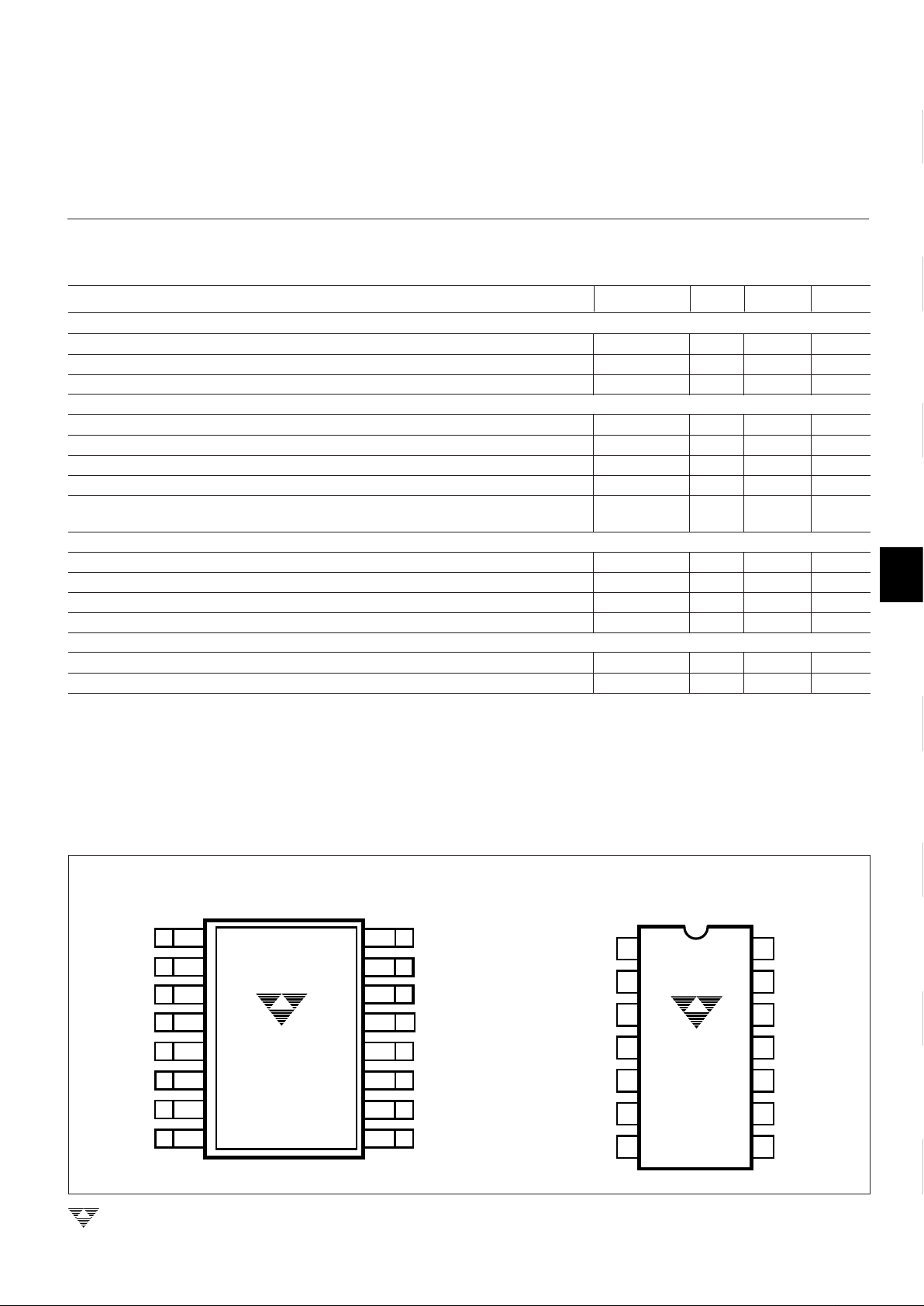
PIN CONFIGURATIONS
1
2
3
4
5
6
7
14
13
12
11
10
9
8
1A
1B
2A
2B
3A
3B
GND
V
1Y
2Y
3Y
4Y
4B
4A
DD
1
2
3
4
5
6
7
8
16
13
12
11
10
9
1A
1B
2A
2B
3A
3B
GND
GND
V
1Y
2Y
3Y
4Y
4B
4A
DD
V
DD
15
14
TC4467/8/9
TC4467/8/9
16-Pin SOIC (Wide) 14-Pin Plastic DIP/CerDIP

4-264
TELCOM SEMICONDUCTOR, INC.
LOGIC-INPUT CMOS
QUAD DRIVERS
TC4467
TC4468
TC4469
Three components make up total package power
dissipation:
(1) Load-caused dissipation (PL)
(2) Quiescent power (PQ)
(3) Transition power (PT).
A capacitive-load-caused dissipation (driving MOSFET
gates), is a direct function of frequency, capacitive load, and
supply voltage. The power dissipation is:
PL = f C V
S
2
,
where: f = Switching frequency
C = Capacitive load
VS = Supply voltage.
A resistive-load-caused dissipation for ground-referenced loads is a function of duty cycle, load current, and
load voltage. The power dissipation is:
PL = D (VS – VL) IL,
where: D = Duty cycle
VS = Supply voltage
VL = Load voltage
IL = Load current.
A resistive-load-caused dissipation for supply-referenced loads is a function of duty cycle, load current, and
output voltage. The power dissipation is:
PL = D VO IL,
where: f = Switching frequency
VO = Device output voltage
IL = Load current.
Quiescent power dissipation depends on input signal
duty cycle. Logic HIGH outputs result in a lower power
dissipation mode, with only 0.6 mA total current drain (all
devices driven). Logic LOW outputs raise the current to 4 mA
maximum. The quiescent power dissipation is:
PQ = VS (D (IH) + (1–D)IL),
where: IH = Quiescent current with all outputs LOW
(4 mA max)
IL = Quiescent current with all outputs HIGH
(0.6 mA max)
D = Duty cycle
VS =Supply voltage.
Supply Bypassing
Large currents are required to charge and discharge
large capacitive loads quickly. For example, charging a
1000 pF load to 18V in 25nsec requires 0.72A from the
device's power supply.
To guarantee low supply impedance over a wide frequency range, a 1 µF film capacitor in parallel with one or two
low-inductance 0.1 µF ceramic disk capacitors with short
lead lengths (<0.5 in.) normally provide adequate bypassing.
Grounding
The TC4467 and TC4469 contain inverting drivers.
Potential drops developed in common ground impedances
from input to output will appear as negative feedback and
degrade switching speed characteristics. Instead, individual
ground returns for input and output circuits, or a ground
plane, should be used.
Input Stage
The input voltage level changes the no-load or quiescent supply current. The N-channel MOSFET input stage
transistor drives a 2.5 mA current source load. With logic "0"
outputs, maximum quiescent supply current is 4 mA. Logic
"1" output level signals reduce quiescent current to 1.4 mA
maximum. Unused driver inputs must be connected to V
DD
or VSS. Minimum power dissipation occurs for logic "1"
outputs.
The drivers are designed with 50 mV of hysteresis. This
provides clean transitions and minimizes output stage current spiking when changing states. Input voltage thresholds
are approximately 1.5V, making any voltage greater than
1.5V up to V
DD
a logic 1 input . Input current is less than 1 µA
over this range.
Power Dissipation
The supply current versus frequency and supply current
versus capacitive load characteristic curves will aid in determining power dissipation calculations. TelCom Semiconductor's CMOS drivers have greatly reduced quiescent DC
power consumption.
Input signal duty cycle, power supply voltage and load
type, influence package power dissipation. Given power
dissipation and package thermal resistance, the maximum
ambient operating temperature is easily calculated. The 14pin plastic package junction-to-ambient thermal resistance
is 83.3°C/W. At +70°C, the package is rated at 800mW
maximum dissipation. Maximum allowable chip temperature is +150°C.

4-265
TELCOM SEMICONDUCTOR, INC.
7
6
5
4
3
1
2
8
LOGIC-INPUT CMOS
QUAD DRIVERS
TC4467
TC4468
TC4469
Maximum operating temperature:
TJ – θJA (PD) = 141°C,
where: TJ = Maximum allowable junction temperature
(+150°C)
θJA = Junction-to-ambient thermal resistance
(83.3°C/W) 14-pin plastic package.
NOTE: Ambient operating temperature should not exceed +85°C for
"EJD" device or +125°C for "MJD" device.
Figure 1. Switching Time Test Circuit
V
OUT
1B
1A
2B
2A
3B
3A
4B
4A
1 µF FILM 0.1 µF CERAMIC
V
DD
470 pF
90%
10%
10%
10%
t
D1
t
R
t
D2
t
F
90%
+5V
INPUT
(A, B)
V
DD
OUTPUT
0V
0V
90%
1
2
3
4
5
6
8
9
7
10
11
12
13
14
Input: 100 kHz, square wave,
t
RISE
= t
FALL
≤ 10nsec
Transition power dissipation arises in the
complementary configuration (TC446X) because the
output stage N-channel and P-channel MOS transistors
are ON simultaneously for a very short period when the
output changes. The transition power dissipation is
approximately:
PT = f VS (10 3 10–9).
Package power dissipation is the sum of load, quiescent and transition power dissipations. An example shows
the relative magnitude for each term:
C = 1000 pF capacitive load
VS= 15V
D = 50%
f = 200 kHz
PD= Package Power Dissipation = PL + PQ + P
T
= 45 mW + 35 mW + 30 mW = 110 mW.

4-266
TELCOM SEMICONDUCTOR, INC.
LOGIC-INPUT CMOS
QUAD DRIVERS
TC4467
TC4468
TC4469
TYPICAL CHARACTERISTICS
140
120
100
80
60
40
20
0
3 5 7 9 11 13 15 17
19
V (V)
SUPPLY
2200 pF
1600 pF
1000 pF
470 pF
100 pF
t (nsec)
(RISE)
Rise Time vs. Supply Voltage
140
120
100
80
60
40
20
0
3 5 7 9 11 13 15 17
19
V (V)
SUPPLY
t (nsec)
(FALL)
100 pF
470 pF
1000 pF
1500 pF
2200 pF
Fall Time vs. Supply Voltage
140
120
100
80
60
40
20
0
100 1000
10,000
C (pF)
LOAD
t (nsec)
(RISE)
10V
15V
5V
Rise Time vs. Capacitive Load
140
120
100
80
60
40
20
0
100 1000
10,000
C (pF)
LOAD
t (nsec)
(FALL)
5V
10V
15V
Fall Time vs. Capacitive Load
0
–50
TEMPERATURE (°C)
TIME (nsec)
5
10
15
20
25
–25 0 25 50 75 100 125
t
V = 17.5V
C = 470 pF
t
SUPPLY
LOAD
(FALL)
(RISE)
Rise/Fall Times vs. Temperature
0
4
DELAY TIME (nsec)
20
40
60
80
812141618610
V (V)
SUPPLY
t
C = 470 pF
LOAD
D1
Propagation Delay Time vs. Supply Voltage
t
D2

4-267
TELCOM SEMICONDUCTOR, INC.
7
6
5
4
3
1
2
8
LOGIC-INPUT CMOS
QUAD DRIVERS
TC4467
TC4468
TC4469
TYPICAL CHARACTERISTICS (Cont.)
140
120
100
80
60
40
20
0
19
10
V (V)
DRIVE
DELAY TIME (nsec)
2345678
INPUT FALLING
t
t
INPUT RISING
V = 12V
DD
D1
D2
Input Amplitude vs. Delay Times
70
20
100
120
TEMPERATURE (°C)
DELAY TIME (nsec)
–40 –20 0 20 40 60 80
30
40
50
60
V = 17.5V
C = 470 pF
V = 0, 5V
DD
LOAD
IN
t
t
D1
D2
Propagation Delay Times vs. Temperature
–60
0
4
0.5
1.0
1.5
2.0
2.5
6 8 10 12 14 16 18
V
SUPPLY
(V)
I (mA)
QUIESCENT
Quiescent Supply Current vs. Supply Voltage
3.5
0
100
120
T (°C)
–40 –20 0 20 40 60 80
3.0
2.5
2.0
1.5
1.0
0.5
I (mA)
QUIESCENT
V = 17.5V
DD
OUTPUTS HIGH
OUTPUTS LOW
JUNCTION
Quiescent Supply Current vs. Temperature
–60
0
4 6 8 1012141618
V
SUPPLY
(V)
5
10
15
20
25
30
35
T = +150°C
T = +25°C
R ( )Ω
DS(ON)
J
High-State Output Resistance
J
0
4
6 8 10 12 14 16 18
5
10
15
20
25
30
35
T = +150°C
T = +25°C
J
J
Low-State Output Resistance
V
SUPPLY
(V)
R ( )Ω
DS(ON)
OUTPUTS = 1
OUTPUTS = 0

4-268
TELCOM SEMICONDUCTOR, INC.
SUPPLY CURRENT CHARACTERISTICS (Load on Single Output Only)
60
0
100 1000
10,000
C (pF)
LOAD
50
40
30
20
10
2 MHz
1 MHz
500 kHz
200 kHz
20 kHz
I (mA)
SUPPLY
V = 18V
DD
Supply Current vs. Capacitive Load
60
0
100 1000
FREQUENCY (kHz)
50
40
30
20
10
I (mA)
SUPPLY
V = 18V
DD
2200 pF
1000 pF
100 pF
10
Supply Current vs. Frequency
10,000
60
0
100 1000
10,000
50
40
30
20
10
C (pF)
LOAD
I (mA)
SUPPLY
V = 12V
DD
2 MHz
1 MHz
500 kHz
200 kHz
20 kHz
Supply Current vs. Capacitive Load
60
0
10 100
FREQUENCY (kHz)
50
40
30
20
10
1000
I (mA)
SUPPLY
2200 pF
1000 pF
100 pF
V = 12V
DD
Supply Current vs. Frequency
10,000
60
50
40
30
20
10
0
100 1000
10,000
C (pF)
LOAD
I (mA)
SUPPLY
1 MHz
500 kHz
200 kHz
20 kHz
2 MHz
V = 6V
DD
Supply Current vs. Capacitive Load
60
0
10 1000
100
FREQUENCY (kHz)
50
40
30
20
10
I (mA)
SUPPLY
V = 6V
DD
2200 pF
1000 pF
100 pF
Supply Current vs. Frequency
10,000
LOGIC-INPUT CMOS
QUAD DRIVERS
TC4467
TC4468
TC4469

4-269
TELCOM SEMICONDUCTOR, INC.
7
6
5
4
3
1
2
8
TYPICAL APPLICATIONS
4.7 kΩ
TC4469
48-Volt, 3-Phase Brushless Output Stage
1
2
3
4
5
6
8
9
1B
2A
2B
3A
3B
4A
4B
1Y
2Y
3Y
4Y
GND
U1
13
12
11
10
TC4469
1
2
3
4
5
6
8
9
1A
1B
2A
2B
3A
3B
4A
4B
1Y
2Y
3Y
4Y
13
12
11
10
48V
14
7
15V
14
7
GND
V
DD
R4
3.3
kΩ
D2
D3 D4
R1
3.3
kΩ
5W
R9
R10
R11
Q1
Q2
Q3
2N5550
2N5550
2N5550
1A
A+
B+
C+
A–
B–
C–
C1
1 µF
D1
1N4744
15V
R2
3.3
kΩ
R3
3.3
kΩ
MOTOR
MOTOR MOTOR
4.7 kΩ
4.7 kΩ
U2
V
DD
PHASE A
PHASE B
PHASE C
(FLOAT AT 33V)
R7
R6
R5
+12V
14
7
1
2
Stepper Motor Drive
TC4469
13
3
4
12
5
6
11
8
9
10
A
B
+5V TO +15V
14
Quad Driver for H-Bridge Motor Control
TC4469
DIRECTION
PWM SPEED
18V
FWD
13
12
11
10
7
9
8
6
5
4
3
2
1
REV
MOTOR
MOTORM
RED
GRAY
YEL
BLK
AIRPAX
#M82102-P2
7.5°/STEP
LOGIC-INPUT CMOS
QUAD DRIVERS
TC4467
TC4468
TC4469
 Loading...