

TelCom Semiconductor Inc TC4432EPA, TC4432EOA, TC4432EJA, TC4432CPA, TC4432COA Datasheet
...
1.5A HIGH-SPEED 30V MOSFET DRIVERS
1
TC4431
TC4432
FEATURES
■ High Peak Output Current ............................... 1.5A
■ Wide Operating Range .............................5V to 30V
■ High Capacitive Load
Drive Capability ......................... 1000 pF in 25nsec
■ Short Delay Time ................................ <78nsec Typ
■ Low Supply Current
— With Logic “1” Input ................................. 2.5mA
— With Logic “0” Input ................................. 300µA
■ Low Output Impedance ....................................... 7Ω
■ Latch-Up Protected .......... Will Withstand >300mA
Reverse Current
■ ESD Protected....................................................4 kV
ORDERING INFORMATION
Temperature
Part No. Package Range
TC4431COA 8-Pin SOIC 0°C to +70°C
TC4431CPA 8-Pin Plastic DIP 0°C to +70°C
TC4431EJA 8-Pin CerDIP – 40°C to +85°C
TC4431EOA 8-Pin SOIC – 40°C to +85°C
TC4431EPA 8-Pin Plastic DIP – 40°C to +85°C
GENERAL DESCRIPTION
The TC4431/4432 are 30V CMOS buffer/drivers suitable for use in high-side driver applications. They will not
latch up under any conditions within their power and voltage
ratings. They can accept, without damage or logic upset, up
to 300mA of reverse current (of either polarity) being forced
back into their outputs. All terminals are fully protected
against up to 4kV of electrostatic discharge.
Under-voltage lockout circuitry forces the output to a
"low" state when the input supply voltage drops below 7V.
Maximum startup VDD bias voltage threshold is 10V. For
operation at lower voltages, the LOCK DIS, Pin 3 can be
grounded to disable the lockout and start-up circuit. The
under-voltage lockout and start-up circuit gives brown out
protection when driving MOSFETS.
Temperature
Part No. Package Range
TC4432COA 8-Pin SOIC 0°C to +70°C
TC4432CPA 8-Pin Plastic DIP 0°C to +70°C
TC4432EJA 8-Pin CerDIP – 40°C to +85°C
TC4432EOA 8-Pin SOIC – 40°C to +85°C
TC4432EPA 8-Pin Plastic DIP – 40°C to +85°C
2
3
4
5
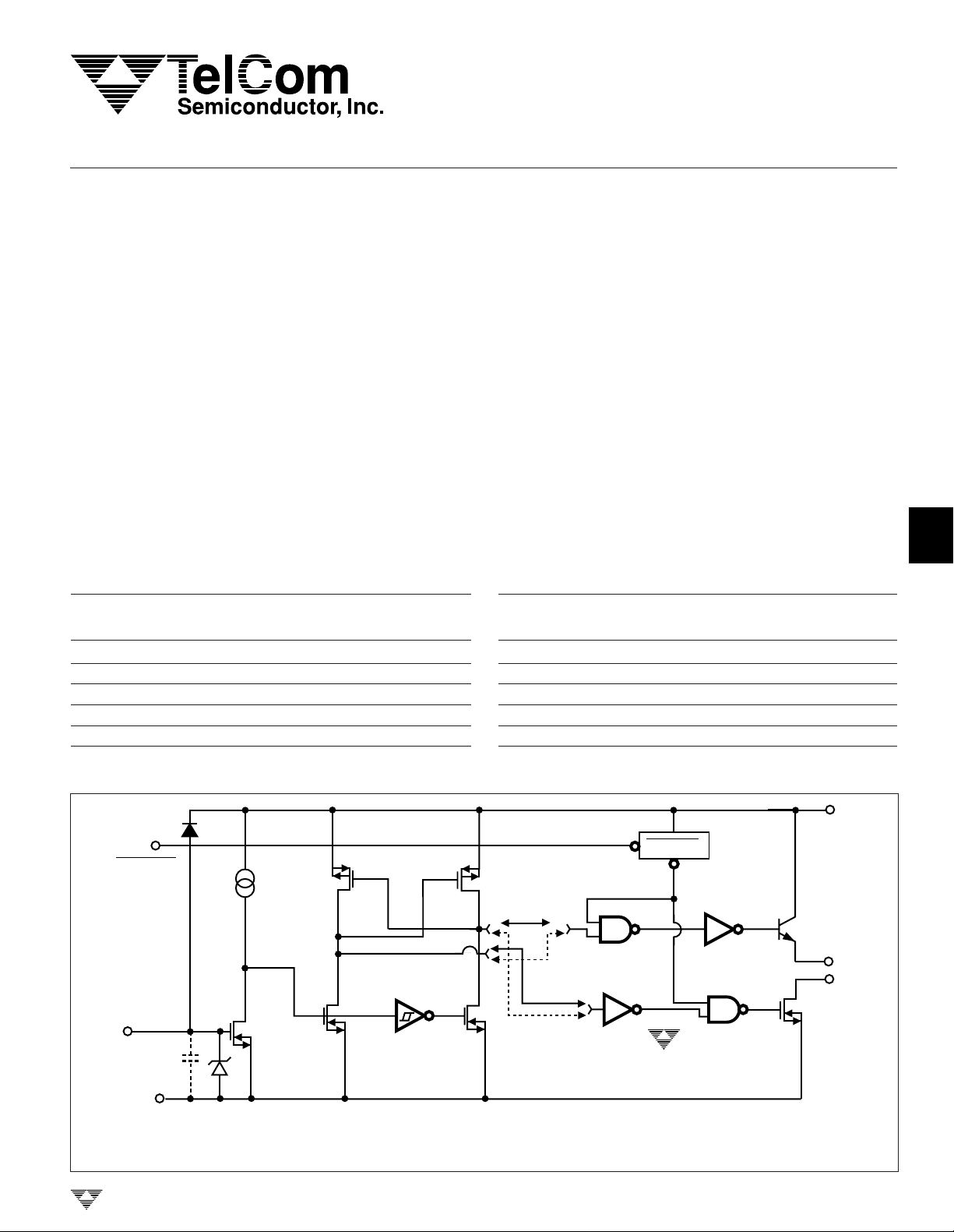
FUNCTIONAL BLOCK DIAGRAM
3
LOCK DIS.
2 mA
INPUT
2
GND
4, 5
EFFECTIVE
INPUT
C = 10pF
TELCOM SEMICONDUCTOR, INC.
250mV
Inverted
TC4431
Non-Inverted
TC4432
UV LOCK
TC4431/32
Inverting/Noninverting
8
V
DD
7
OUT
OUT
6
TC4431/2-8 10/21/96
4-257
6
7
8

TC4431
TC4431
1.5A HIGH-SPEED 30V MOSFET DRIVERS
ABSOLUTE MAXIMUM RATINGS*
Operating Temperature Range
C Version...............................................0°C to +70°C
Supply Voltage ............................................................36V
Input Voltage (Note 1) ........................ V
+ 0.3V to GND
DD
Maximum Chip Temperature................................. +150°C
Storage Temperature Range ................– 65°C to +150°C
Lead Temperature (Soldering, 10 sec) .................+300°C
Package Thermal Resistance
CerDIP R
CerDIP R
PDIP R
PDIP R
SOIC R
SOIC R
ELECTRICAL CHARACTERISTICS: T
................................................ 150°C/W
θJ-A
.................................................. 50°C/W
θJ-C
................................................... 125°C/W
θJ-A
..................................................... 42°C/W
θJ-C
................................................... 250°C/W
θJ-A
..................................................... 75°C/W
θJ-C
= +25°C with 5.0 ≤ V
A
E Version ...........................................- 40°C to +85°C
Package Power Dissipation (TA ≤ 70°C )
Plastic .............................................................730mW
CerDIP............................................................800mW
SOIC...............................................................470mW
*Static-sensitive device. Unused devices must be stored in conductive
material. Protect devices from static discharge and static fields. Stresses
above those listed under "Absolute Maximum Ratings" may cause permanent damage to the device. These are stress ratings only and functional
operation of the device at these or any other conditions above those
indicated in the operation sections of the specifications is not implied.
Exposure to absolute maximum rating conditions for extended periods may
affect device reliability.
≤ 30V, unless otherwise specified.
DD
Symbol Parameter Test Conditions Min Typ Max Unit
Input
V
IH
V
IL
I
IN
Logic 1 High Input Voltage 2.4 — — V
Logic 0 Low Input Voltage — — 0.8 V
Input Current (Note 1) 0V ≤ VIN ≤ V
(16V MAX) –1 — 1 µA
DD
Output
V
V
R
I
PK
I
REV
OH
OL
O
High Output Voltage I
= 100mA V
OUT
– 1.0 V
DD
– 0.8 — V
DD
Low Output Voltage — — 0.025 V
Output Resistance (VOL)V
= 30V, IO = 10mA — 7 10 Ω
DD
Peak Output Current Source: VDD = 30V — 3.0 — A
Sink: VDD = 30V — 1.5 —
Latch-Up Protection Duty Cycle ≤ 2% 0.3 — — A
Withstand Reverse Current t ≤ 300 µsec
Switching Time (Note 2)
t
R
t
F
t
D1
t
D2
Rise Time Figure 1 — 25 40 nsec
Fall Time Figure 1 — 33 50 nsec
Delay Time Figure 1 — 62 80 nsec
Delay Time Figure 1 — 78 90 nsec
Power Supply
I
S
V
S
V
DO
Power Supply Current VIN = 3V — 2.5 4 mA
VIN = 0V — 0.3 0.4
Start-up Threshold — 8.4 10 V
Drop-out Threshold (Note 3) 7 7.7 — V
4-258
TELCOM SEMICONDUCTOR, INC.
 Loading...