

TelCom Semiconductor Inc TC4426MJA, TC4426EPA, TC4426EOA, TC4428COA, TC4427CPA Datasheet
...
1.5A DUAL HIGH-SPEED, POWER MOSFET DRIVERS
FEATURES
GENERAL DESCRIPTION
TC4426
1
TC4427
TC4428
2
■ High Peak Output Current ............................... 1.5A
■ Wide Operating Range ..........................4.5V to 18V
■ High Capacitive Load
Drive Capability ........................ 1000 pF in 25 nsec
■ Short Delay Time ................................ <40nsec Typ
■ Consistent Delay Times With Changes in
Supply Voltage
■ Low Supply Current
— With Logic “1” Input .................................... 4mA
— With Logic “0” Input ................................. 400µA
■ Low Output Impedance ....................................... 7Ω
■ Latch-Up Protected: Will Withstand >0.5A
Reverse Current................................. Down to – 5V
■ Input Will Withstand Negative Inputs
■ ESD Protected.....................................................4kV
■ Pinout Same as TC426/TC427/TC428
ORDERING INFORMATION
Temperature
Part No. Package Range
TC4426COA 8-Pin SOIC 0°C to +70°C
TC4426CPA 8-Pin Plastic DIP 0°C to +70°C
TC4426EOA 8-Pin SOIC – 40°C to +85°C
TC4426EPA 8-Pin Plastic DIP – 40°C to +85°C
TC4426MJA 8-Pin CerDIP – 55°C to +125°C
TC4427COA 8-Pin SOIC 0°C to +70°C
TC4427CPA 8-Pin Plastic DIP 0°C to +70°C
TC4427EOA 8-Pin SOIC – 40°C to +85°C
TC4427EPA 8-Pin Plastic DIP – 40°C to +85°C
TC4427MJA 8-Pin CerDIP – 55°C to +125°C
TC4428COA 8-Pin SOIC 0°C to +70°C
TC4428CPA 8-Pin Plastic DIP 0°C to +70°C
TC4428EOA 8-Pin SOIC – 40°C to +85°C
TC4428EPA 8-Pin Plastic DIP – 40°C to +85°C
TC4428MJA 8-Pin CerDIP – 55°C to +125°C
The TC4426/4427/4428 are improved versions of the
earlier TC426/427/428 family of buffer/drivers (with which
they are pin compatible). They will not latch up under any
conditions within their power and voltage ratings. They are
not subject to damage when up to 5V of noise spiking (of
either polarity) occurs on the ground pin. They can accept,
without damage or logic upset, up to 500mA of reverse
current (of either polarity) being forced back into their
outputs. All terminals are fully protected against up to 4kV of
electrostatic discharge.
As MOSFET drivers, the TC4426/4427/4428 can easily
switch 1000 pF gate capacitances in under 30nsec, and
provide low enough impedances in both the ON and OFF
states to ensure the MOSFET's intended state will not be
affected, even by large transients.
Other compatible drivers are the TC4426A/27A/28A.
These drivers have matched input to output leading edge
and falling edge delays, tD1 and tD2, for processing short
duration pulses in the 25 nanoseconds range. They are pin
compatible with the TC4426/27/28.
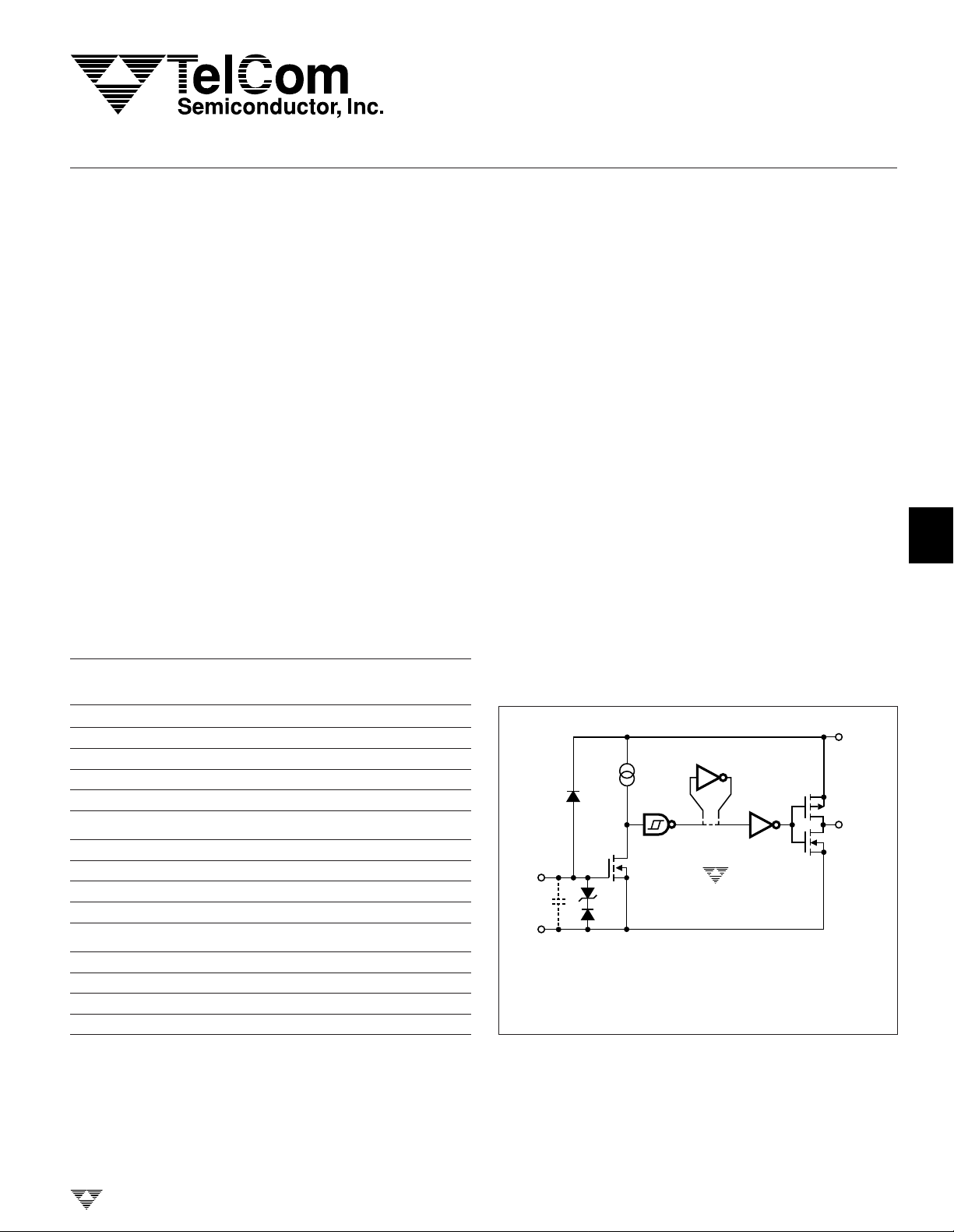
FUNCTIONAL BLOCK DIAGRAM
V
INVERTING
OUTPUTS
300 mV
NONINVERTING
OUTPUTS
INPUT
GND
EFFECTIVE INPUT
C = 12 pF
NOTES: 1.TC4426 has 2 inverting drivers; TC4427 has 2 noninverting drivers.
2. TC4428 has one inverting and one noninverting driver.
3. Ground any unused driver input.
4.7V
TC4426/TC4427/TC4428
DD
OUTPUT
3
4
5
6
7
TELCOM SEMICONDUCTOR, INC.
8
TC4426/7/8-8 10/21/96
4-245
TC4426
TC4427
TC4428
1.5A DUAL HIGH-SPEED
POWER MOSFET DRIVERS
ABSOLUTE MAXIMUM RATINGS*
Supply Voltage ......................................................... +22V
Input Voltage, IN A or IN B. (VDD + 0.3V) to (GND – 5.0V)
Maximum Chip Temperature................................. +150°C
Storage Temperature Range ................– 65°C to +150°C
Lead Temperature (Soldering, 10 sec) .................+300°C
Package Thermal Resistance
CerDIP R
CerDIP R
PDIP R
PDIP R
SOIC R
SOIC R
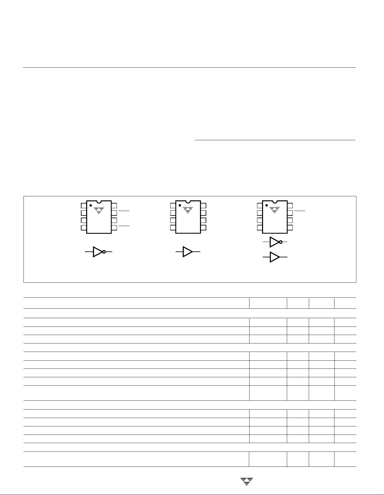
PIN CONFIGURATIONS
................................................ 150°C/W
θJ-A
.................................................. 50°C/W
θJ-C
................................................... 125°C/W
θJ-A
..................................................... 42°C/W
θJ-C
................................................... 155°C/W
θJ-A
..................................................... 45°C/W
θJ-C
1
NC
2
IN A
GND
IN B
NC = NO INTERNAL CONNECTION
NOTE: SOIC pinout is identical to DIP.
TC4426
3
4
2,4 7,5
INVERTING
8
7
6
5
NC
OUT A
V
DD
OUT B
NC
IN A
GND
IN B
1
2
3
4
2,4 7,5
NONINVERTING
Operating Temperature Range
C Version............................................... 0°C to +70°C
E Version ..........................................– 40°C to +85°C
M Version .......................................– 55°C to +125°C
Package Power Dissipation (TA ≤ 70°C)
Plastic .............................................................730mW
CerDIP............................................................800mW
SOIC...............................................................470mW
*Static-sensitive device. Unused devices must be stored in conductive
material. Protect devices from static discharge and static fields. Stresses
above those listed under "Absolute Maximum Ratings" may cause permanent damage to the device. These are stress ratings only and functional
operation of the device at these or any other conditions above those
indicated in the operation sections of the specifications is not implied.
Exposure to absolute maximum rating conditions for extended periods may
affect device reliability.
NC
8
OUT A
7
V
6
DD
5
OUT B
7
5
TC4427
8
7
6
5
NC
OUT A
V
DD
OUT B
NC
IN A
GND
IN B
1
2
TC4428
3
4
2
4
DIFFERENTIAL
ELECTRICAL CHARACTERISTICS: T
= +25°C with 4.5V ≤ V
A
≤ 18V, unless otherwise specified.
DD
Symbol Parameter Test Conditions Min Typ Max Unit
Input
V
IH
V
IL
I
IN
Logic 1 High Input Voltage 2.4 — — V
Logic 0 Low Input Voltage — — 0.8 V
Input Current 0V ≤ VIN ≤ V
DD
– 1 — 1 µA
Output
V
V
R
I
PK
I
REV
OH
OL
O
High Output Voltage VDD – 0.025 — — V
Low Output Voltage — — 0.025 V
Output Resistance VDD = 18V, IO = 10 mA — 7 10 Ω
Peak Output Current Duty Cycle ≤ 2%, t ≤ 30 µsec — 1.5 — A
Latch-Up Protection Duty Cycle ≤ 2% > 0.5 — — A
Withstand Reverse Current t ≤ 30 µsec
Switching Time (Note 1)
t
R
t
F
t
D1
t
D2
Rise Time Figure 1 — 19 30 nsec
Fall Time Figure 1 — 19 30 nsec
Delay Time Figure 1 — 20 30 nsec
Delay Time Figure 1 — 40 50 nsec
Power Supply
I
S
NOTE: 1. Switching times are guaranteed by design.
Power Supply Current VIN = 3V (Both Inputs) — — 4.5 mA
VIN = 0V (Both Inputs) — — 0.4 mA
4-246
TELCOM SEMICONDUCTOR, INC.
 Loading...