

TelCom Semiconductor Inc TC4425MJA, TC4425EPA, TC4425EOE, TC4425CPA, TC4425COE Datasheet
...
3A DUAL HIGH-SPEED POWER MOSFET DRIVERS
TC4423
TC4424
TC4425
1
FEATURES
■ High Peak Output Current .................................. 3A
■ Wide Operating Range ..........................4.5V to 18V
■ High Capacitive Load
Drive Capability ......................... 1800 pF in 25nsec
■ Short Delay Times ............................. < 40nsec Typ
■ Matched Rise/Fall Times
■ Low Supply Current
— With Logic "1" Input ................................ 3.5 mA
— With Logic "0" Input ................................ 350 µA
■ Low Output Impedance ............................. 3.5Ω Typ
■ Latch-Up Protected . Will Withstand 1.5A Reverse
Current
■ Logic Input Will Withstand Negative Swing Up
to 5V
■ ESD Protected....................................................4 kV
■ Pinouts Same as TC1426/27/28; TC4426/27/28
ORDERING INFORMATION
Temperature
Part No. Package Range
TC4423COE 16-Pin SOIC (Wide) 0°C to +70°C
TC4423CPA 8-Pin Plastic DIP 0°C to +70°C
TC4423EOE 16-Pin SOIC (Wide) – 40°C to +85°C
TC4423EPA 8-Pin Plastic DIP – 40°C to +85°C
TC4423MJA 8-Pin CerDIP – 55°C to +125°C
TC4424COE 16-Pin SOIC (Wide) 0°C to +70°C
TC4424CPA 8-Pin Plastic DIP 0°C to +70°C
TC4424EOE 16-Pin SO Wide – 40°C to +85°C
GENERAL DESCRIPTION
The TC4423/4424/4425 are higher output current versions of the new TC4426/4427/4428 buffer/drivers, which,
in turn, are improved versions of the earlier TC426/427/428
series. All three families are pin-compatible. The TC4423/
4424/4425 drivers are capable of giving reliable service in
far more demanding electrical environments than their antecedents.
Although primarily intended for driving power MOSFETs,
the TC4423/4424/4425 drivers are equally well-suited to
driving any other load (capacitive, resistive, or inductive)
which requires a low impedance driver capable of high peak
currents and fast switching times. For example, heavily
loaded clock lines, coaxial cables, or piezoelectric transducers can all be driven from the TC4423/4424/4425. The only
known limitation on loading is the total power dissipated in
the driver must be kept within the maximum power dissipation limits of the package.
Temperature
Part No Package Range
TC4424EPA 8-Pin Plastic DIP – 40°C to +85°C
TC4424MJA 8-Pin CerDIP – 55°C to +125°C
TC4425COE 16-Pin SO Wide 0°C to +70°C
TC4425CPA 8-Pin Plastic DIP 0°C to +70°C
TC4425EOE 16-Pin SO Wide – 40°C to +85°C
TC4425EPA 8-Pin Plastic DIP – 40°C to +85°C
TC4425MJA 8-Pin CerDIP – 55°C to +125°C
2
3
4
5
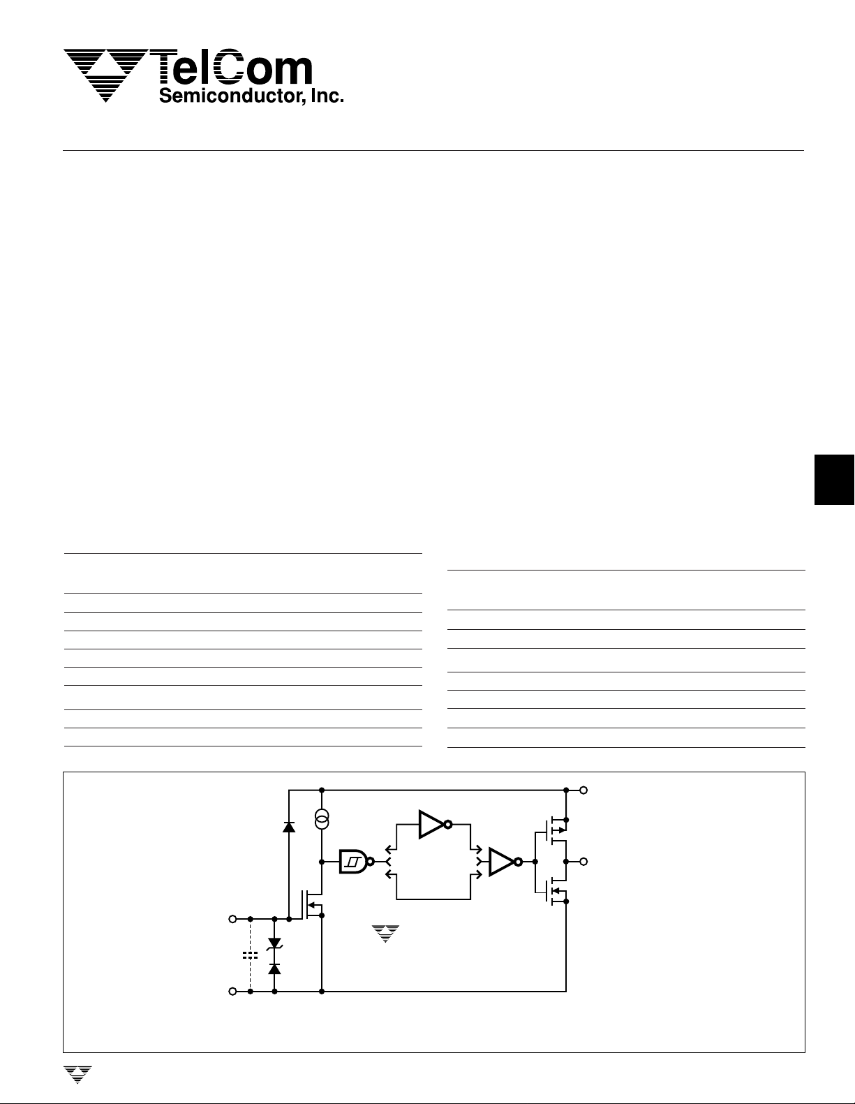
FUNCTIONAL BLOCK DIAGRAM
INPUT
GND
EFFECTIVE
INPUT C = 20 pF
(EACH INPUT)
TELCOM SEMICONDUCTOR, INC.
4.7V
V
INVERTING
300 mV
NONINVERTING
TC4423
TC4424
TC4425
NOTES:
1. TC4425 has one inverting and one noninverting driver.
2. Ground any unused driver input.
DUAL INVERTING
DUAL NONINVERTING
ONE INV., ONE NONINV.
DD
OUTPUT
6
7
8
TC4423/4/5-6 10/21/96
4-237
TC4423
TC4424
TC4425
3A DUAL HIGH-SPEED
POWER MOSFET DRIVERS
ABSOLUTE MAXIMUM RATINGS*
Supply Voltage ......................................................... +22V
Input Voltage, IN A or IN B......VDD + 0.3V to GND – 5.0V
Maximum Chip Temperature.................................+150°C
Storage Temperature Range ................– 65°C to +150°C
Lead Temperature (Soldering, 10 sec) .................+300°C
Package Thermal Resistance
CerDIP R
CerDIP R
PDIP R
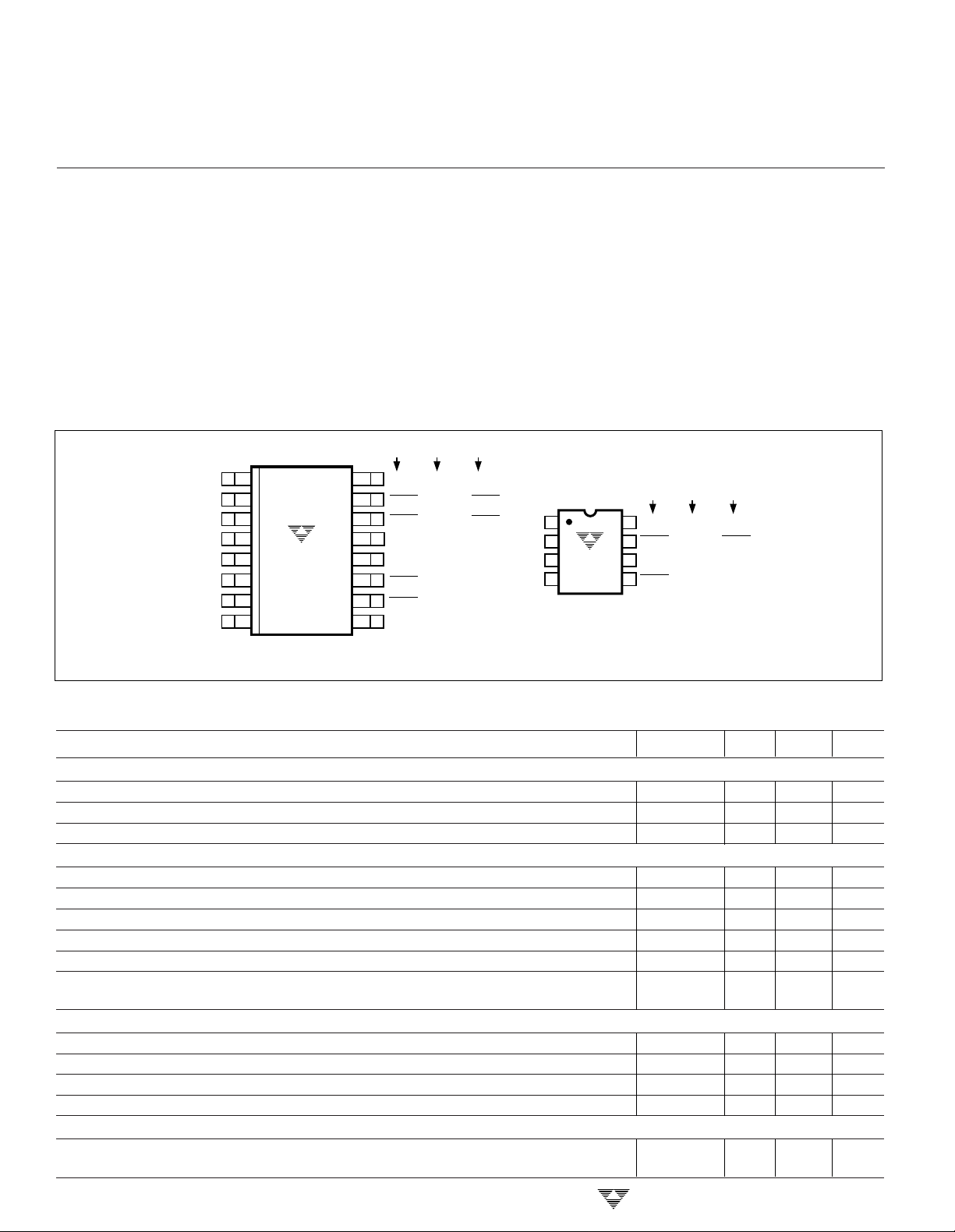
PIN CONFIGURATIONS
................................................ 150°C/W
θJ-A
.................................................. 55°C/W
θJ-C
................................................... 125°C/W
θJ-A
16-Pin SO Wide
1
NC
IN A
GND
GND
IN B
2
NC
3
4
TC4423
5
TC4424
NC
NC
NC = NO CONNECTION
NOTE: Duplicate pins must both be connected for proper operation.
TC4425
6
7
8
4423 4424 4425
16
15
14
13
12
11
10
9
NC
OUT A
OUT A
V
DD
V
DD
OUT B
OUT B
NC
NC
OUT A
OUT A
V
DD
V
DD
OUT B
OUT B
NC
PDIP R
SOIC R
SOIC R
..................................................... 45°C/W
θJ-C
................................................... 155°C/W
θJ-A
..................................................... 75°C/W
θJ-C
Operating Temperature Range
C Version...............................................0°C to +70°C
I Version ............................................- 25°C to +85°C
E Version ...........................................- 40°C to +85°C
M Version ........................................- 55°C to +125°C
Package Power Dissipation (TA ≤ 70°C)
Plastic DIP ......................................................730mW
CerDIP............................................................800mW
SOIC...............................................................470mW
NC
OUT A
OUT A
V
DD
V
DD
OUT B
OUT B
NC
NC
IN A
GND
IN B
1
2
3
4
8-Pin DIP
TC4423
TC4424
TC4425
4423 4424 4425
8
NC
NC
OUT A
OUT A
7
6
5
V
DD
OUT B
V
DD
OUT B
NC
OUT A
V
DD
OUT B
ELECTRICAL CHARACTERISTICS: T
= +25°C with 4.5V ≤ VDD ≤ 18V, unless otherwise specified.
A
Symbol Parameter Test Conditions Min Typ Max Unit
Input
V
OH
V
IL
I
IN
Logic 1 High Input Voltage 2.4 — — V
Logic 0 Low Input Voltage — — 0.8 V
Input Current 0V ≤ VIN ≤ V
DD
– 1 — 1 µA
Output
V
V
R
R
I
PK
I
REV
OH
OL
O
O
High Output Voltage V
– 0.025 — — V
DD
Low Output Voltage — — 0.025 V
Output Resistance, High I
Output Resistance, Low I
= 10 mA, VDD = 18V — 2.8 5 Ω
OUT
= 10 mA, VDD = 18V — 3.5 5 Ω
OUT
Peak Output Current — 3 — A
Latch-Up Protection Duty Cycle ≤ 2% 1.5 — — A
Withstand Reverse Current t ≤ 300 µsec
Switching Time (Note 1)
t
R
t
F
t
D1
t
D2
Rise Time Figure 1, CL = 1800 pF — 23 35 nsec
Fall Time Figure 1, CL = 1800 pF — 25 35 nsec
Delay Time Figure 1, CL = 1800 pF — 33 75 nsec
Delay Time Figure 1, CL = 1800 pF — 38 75 nsec
Power Supply
I
S
Power Supply Current VIN = 3V (Both Inputs) — 1.5 2.5 mA
VIN = 0V (Both Inputs) — 0.15 0.25 mA
4-238
TELCOM SEMICONDUCTOR, INC.
3A DUAL HIGH-SPEED
POWER --MOSFET DRIVERS
ELECTRICAL CHARACTERISTICS (Cont.):
1
TC4423
TC4424
TC4425
Over operating temperature range with 4.5V ≤ VDD ≤ 18V, unless otherwise specified.
Symbol Parameter Test Conditions Min Typ Max Unit
Input
V
IH
V
IL
I
IN
Logic 1 High Input Voltage 2.4 — — V
Logic 0 Low Input Voltage — — 0.8 V
Input Current 0V ≤ VIN ≤ V
DD
– 10 — 10 µA
Output
V
V
R
R
I
PK
I
REV
OH
OL
O
O
High Output Voltage V
Low Output Voltage — — 0.025 V
Output Resistance, High I
Output Resistance, Low I
Peak Output Current — 3 — A
Latch-Up Protection Duty Cycle ≤ 2% 1.5 — — A
Withstand Reverse Current t ≤ 300 µsec
= 10 mA, VDD = 18V — 3.7 8 Ω
OUT
= 10 mA, VDD = 18V — 4.3 8 Ω
OUT
– 0.025 — — V
DD
Switching Time (Note 1)
t
R
t
F
t
D1
t
D2
Rise Time Figure 1, CL = 1800 pF — 28 60 nsec
Fall Time Figure 1, CL = 1800 pF — 32 60 nsec
Delay Time Figure 1, CL = 1800 pF — 32 100 nsec
Delay Time Figure 1, CL = 1800 pF — 38 100 nsec
Power Supply
I
S
NOTE: 1. Switching times guaranteed by design.
Power Supply Current VIN = 3V (Both Inputs) — 2 3.5 mA
VIN = 0V (Both Inputs) — 0.2 0.3
2
3
4
5
Test Circuit
INPUT
INPUT: 100 kHz,
square wave,
t
= t
RISE
FALL
≤ 10 nsec
+5V
INPUT
10%
0V
16V
OUTPUT
0V
Figure 1. Inverting Driver Switching Time
t
D1
90%
10%
V
DD
1
2
TC4423
(1/2 TC4425)
t
F
TELCOM SEMICONDUCTOR, INC.
= 16V
1 µF
WIMA
MKS-2
0.1 µF CERAMIC
OUTPUT
C = 1800pF
L
90%
t
D2
t
R
10%
90%
Test Circuit
INPUT: 100 kHz,
square wave,
t
= t
RISE
≤ 10 nsec
+5V
INPUT
0V
16V
OUTPUT
0V
V
= 16V
DD
1 µF
WIMA
MKS-2
INPUT
FALL
10%
t
D1
Figure 2. Noninverting Driver Switching Time
1
2
(1/2 TC4425)
90%
10%
TC4424
t
R
0.1 µF CERAMIC
OUTPUT
C = 1800pF
L
90%
t
D2
10%
90%
t
F
4-239
6
7
8
 Loading...