

TelCom Semiconductor Inc TC4429MJA, TC4429IJA, TC4429EPA, TC4429EOA, TC4429CPA Datasheet
...
6A HIGH-SPEED MOSFET DRIVERS
FEATURES
1
TC4420
TC4429
2
GENERAL DESCRIPTION
■ Latch-Up Protected ............. Will Withstand > 1.5A
Reverse Output Current
■ Logic Input Will Withstand Negative Swing Up
to 5V
■ ESD Protected.....................................................4kV
■ Matched Rise and Fall Times ......................25nsec
■ High Peak Output Current ......................... 6A Peak
■ Wide Operating Range ..........................4.5V to 18V
■ High Capacitive Load Drive .....................10,000 pF
■ Short Delay Time .................................. 55nsec Typ
■ Logic High Input, Any Voltage .............2.4V to V
DD
■ Low Supply Current With Logic "1" Input ... 450µA
■ Low Output Impedance .................................... 2.5Ω
■ Output Voltage Swing to Within 25mV of Ground
or V
DD
APPLICATIONS
■ Switch-Mode Power Supplies
■ Motor Controls
■ Pulse Transformer Driver
■ Class D Switching Amplifiers
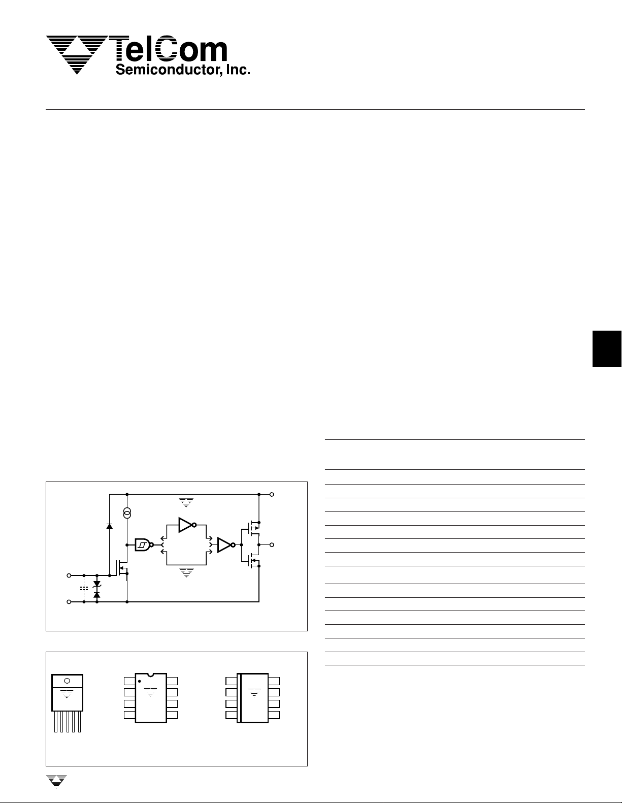
FUNCTIONAL BLOCK DIAGRAM
V
DD
500 µA
300 mV
INPUT
GND
4.7V
EFFECTIVE
INPUT
C = 38 pF
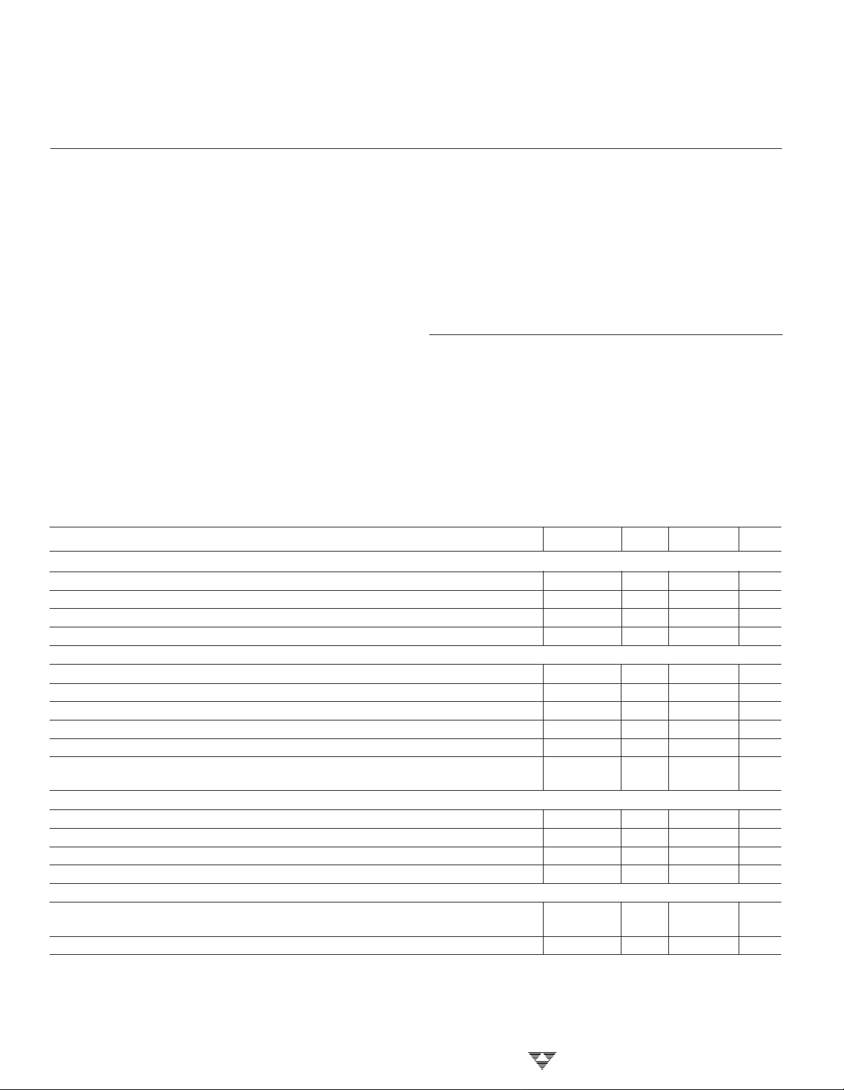
PIN CONFIGURATIONS
TO-220-5
TC4420
TC4429
DD
V
GND
INPUT
Tab is
Connected
to V
GND
OUTPUT
INPUT
DD
8-Pin DIP
V
18
DD
27
TC4420
36
NC
TC4429
45
NOTE: Duplicate pins must
TC4429
TC4420
V
OUTPUT
OUTPUT
GNDGND
V
DD
both
be connected for proper operation.
18
DD
27
INPUT
36
NC
45
8-Pin SOIC
TC4420
TC4429
OUTPUT
V
DD
OUTPUT
OUTPUT
GNDGND
The TC4420/4429 are 6A (peak), single output MOSFET
drivers. The TC4429 is an inverting driver (pin-compatible
with the TC429), while the TC4420 is a non-inverting driver.
These drivers are fabricated in CMOS for lower power, more
efficient operation versus bipolar drivers.
Both devices have TTL-compatible inputs, which can be
driven as high as VDD + 0.3V or as low as – 5V without upset
or damage to the device. This eliminates the need for
external level shifting circuitry and its associated cost and
size. The output swing is rail-to-rail ensuring better drive
voltage margin, especially during power up/power down
sequencing. Propagational delay time is only 55nsec (typ.)
and the output rise and fall times are only 25nsec (typ.) into
2500pF across the usable power supply range.
Unlike other drivers, the TC4420/4429 are virtually
latch-up proof. They replace three or more discrete components saving PCB area, parts and improving overall system
reliability.
ORDERING INFORMATION
Temp.
Part No. Logic Package Range
TC4420CAT Noninverting 5-Pin TO-220 0°C to +70°C
TC4420COA Noninverting 8-Pin SOIC 0°C to +70°C
TC4420CPA Noninverting 8-Pin PDIP 0°C to +70°C
TC4420EOA Noninverting 8-Pin SOIC – 40°C to +85°C
TC4420EPA Noninverting 8-Pin PDIP – 40°C to +85°C
TC4420IJA Noninverting 8-Pin CerDIP –25°C to +85°C
TC4420MJA Noninverting 8-Pin CerDIP – 55°C to +125°C
TC4429CAT Inverting 5-Pin TO-220 0°C to +70°C
TC4429COA Inverting 8-Pin SOIC 0°C to +70°C
TC4429CPA Inverting 8-Pin PDIP 0°C to +70°C
TC4429EOA Inverting 8-Pin SOIC – 40°C to +85°C
TC4429EPA Inverting 8-Pin PDIP – 40°C to +85°C
TC4429IJA Inverting 8-Pin CerDIP – 25°C to +85°C
TC4429MJA Inverting 8-Pin CerDIP – 55°C to +125°C
TC4420/9-6 10/18/96
3
4
5
6
7
8
TELCOM SEMICONDUCTOR, INC.
4-225
TC4420
TC4429
ABSOLUTE MAXIMUM RATINGS*
6A HIGH-SPEED MOSFET DRIVERS
Supply Voltage ......................................................... +20V
Input Voltage ............................................... – 5V to > V
Input Current (VIN > VDD) .........................................50mA
Power Dissipation, TA ≤ 70°C
PDIP ...............................................................730mW
SOIC...............................................................470mW
CerDIP............................................................800mW
5-Pin TO-220 ......................................................1.6W
Package Power Dissipation (TA ≤ 70°C)
5-Pin TO-220 (With Heat Sink).........................1.60W
Derating Factors (To Ambient)
PDIP ............................................................. 8mW/°C
SOIC............................................................. 4mW/°C
CerDIP....................................................... 6.4mW/°C
5-Pin TO-220 .............................................. 12mW/°C
Storage Temperature Range ................– 65°C to +150°C
Operating Temperature (Chip) ..............................+150°C
DD
Operating Temperature Range (Ambient)
C Version............................................... 0°C to +70°C
I Version ...........................................– 25°C to +85°C
E Version ..........................................– 40°C to +85°C
M Version .......................................– 55°C to +125°C
Lead Temperature (Soldering, 10 sec) .................+300°C
*Static-sensitive device. Unused devices must be stored in conductive
material. Protect devices from static discharge and static fields. Stresses
above those listed under "Absolute Maximum Ratings" may cause permanent damage to the device. These are stress ratings only and functional
operation of the device at these or any other conditions above those
indicated in the operation sections of the specifications is not implied.
Exposure to absolute maximum rating conditions for extended periods may
affect device reliability.
Thermal Impedances (To Case)
5-Pin TO-220 R
ELECTRICAL CHARACTERISTICS: T
........................................ 10°C/W
θJ-C
A
= +25°C with 4.5V ≤ V
≤ 18V, unless otherwise specified.
DD
Symbol Parameter Test Conditions Min Typ Max Unit
Input
V
IH
V
IL
VIN (Max) Input Voltage Range –5 — VDD+0.3 V
I
IN
Logic 1 High Input Voltage 2.4 1.8 — V
Logic 0 Low Input Voltage — 1.3 0.8 V
Input Current 0V ≤ VIN ≤ V
DD
– 10 — 10 µA
Output
V
V
R
R
I
PK
I
REV
OH
OL
O
O
High Output Voltage See Figure 1 V
– 0.025 — — V
DD
Low Output Voltage See Figure 1 — — 0.025 V
Output Resistance, High I
Output Resistance, Low I
= 10 mA, VDD = 18V — 2.1 2.8 Ω
OUT
= 10 mA, VDD = 18V — 1.5 2.5 Ω
OUT
Peak Output Current VDD = 18V (See Figure 5) — 6 — A
Latch-Up Protection Duty Cycle ≤ 2% 1.5 — — A
Withstand Reverse Current t ≤ 300 µs
Switching Time (Note 1)
t
R
t
F
t
D1
t
D2
Rise Time Figure 1, CL = 2500 pF — 25 35 nsec
Fall Time Figure 1, CL = 2500 pF — 25 35 nsec
Delay Time Figure 1 — 55 75 nsec
Delay Time Figure 1 — 55 75 nsec
Power Supply
I
S
V
DD
Power Supply Current VIN = 3V — 0.45 1.5 mA
VIN = 0V — 55 150 µA
Operating Input Voltage 4.5 — 18 V
4-226
TELCOM SEMICONDUCTOR, INC.
 Loading...