

TelCom Semiconductor Inc TC429EPA, TC429CPA, TC429MJA Datasheet
6A SINGLE HIGH-SPEED, CMOS POWER MOSFET DRIVER
1
TC429
FEATURES
■ High Peak Output Current .................................. 6A
■ Wide Operating Range .............................7V to 18V
■ High-Impedance CMOS Logic Input
■ Logic Input Threshold Independent of
Supply Voltage
■ Low Supply Current
— With Logic 1 Input................................ 5mA Max
— With Logic 0 Input............................. 0.5mA Max
■ Output Voltage Swing Within 25 mV of Ground
or V
DD
■ Short Delay Time .................................. 75nsec Max
■ High Capacitive Load Drive Capability
— t
RISE
, t
= 35nsec Max With C
FALL
LOAD
= 2500pF
APPLICATIONS
■ Switch-Mode Power Supplies
■ CCD Drivers
■ Pulse Transformer Drive
■ Class D Switching Amplifiers
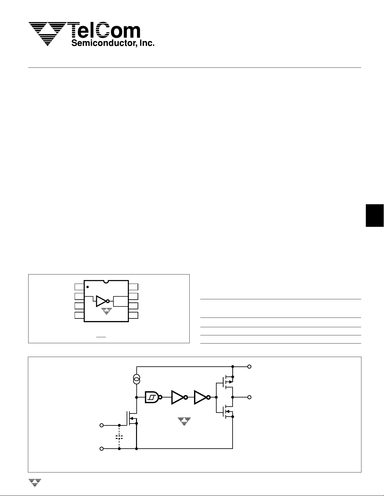
PIN CONFIGURATION
V
18
DD
27
INPUT
36
NC
45
NC = NO INTERNAL CONNECTION
NOTE: Duplicate pins must both be connected for proper operation.
TYPICAL APPLICATION
TC429
V
DD
OUTPUT
OUTPUT
GNDGND
GENERAL DESCRIPTION
The TC429 is a high-speed, single CMOS-level translator and driver. Designed specifically to drive highly capacitive power MOSFET gates, the TC429 features 2.5Ω output
impedance and 6A peak output current drive.
A 2500pF capacitive load will be driven 18V in 25nsec.
Delay time through the device is 60nsec. The rapid switching
times with large capacitive loads minimize MOSFET transition power loss.
A TTL/CMOS input logic level is translated into an
output voltage swing that equals the supply and will swing
to within 25mV of ground or VDD. Input voltage swing may
equal the supply. Logic input current is under 10µA, making
direct interface to CMOS/bipolar switch-mode power supply
controllers easy. Input "speed-up" capacitors are not
required.
The CMOS design minimizes quiescent power supply
current. With a logic 1 input, power supply current is 5mA
maximum and decreases to 0.5mA for logic 0 inputs.
For dual devices, see the TC426/TC427/TC428
data sheet.
For noninverting applications, or applications requiring
latch-up protection, see the TC4420/TC4429 data sheet.
ORDERING INFORMATION
Temperature
Part No. Package Range
TC429CPA 8-Pin Plastic DIP 0°C to +70°C
TC429EPA 8-Pin Plastic DIP – 40°C to +85°C
TC429MJA 8-Pin CerDIP – 55°C to +125°C
1,8
V
DD
2
3
4
5
6
INPUT
GND
TELCOM SEMICONDUCTOR, INC.
2
4,5
EFFECTIVE
INPUT
C = 38pF
300mV
TC429
6,7
OUTPUT
7
8
TC429-4 10/11/96
4-175
TC429
6A SINGLE HIGH-SPEED,
CMOS POWER MOSFET DRIVER
ABSOLUTE MAXIMUM RATINGS*
Supply Voltage ......................................................... +20V
Input Voltage, Any Terminal.....VDD +0.3V to GND – 0.3V
Power Dissipation (TA ≤ 70°C)
Plastic DIP ......................................................730mW
CerDIP............................................................800mW
Derating Factors
Plastic DIP ............................ 5.6 mW/°C Above 36°C
CerDIP...................................................... 6.4 mW/°C
Operating Temperature Range
Maximum Chip Temperature.................................+150°C
Storage Temperature Range ................– 65°C to +150°C
Lead Temperature (Soldering, 10 sec) .................+300°C
*Static-sensitive device. Unused devices must be stored in conductive
material. Protect devices from static discharge and static fields. Stresses
above those listed under Absolute Maximum Ratings may cause permanent damage to the device. These are stress ratings only and functional
operation of the device at these or any other conditions above those
indicated in the operational sections of the specifications is not implied.
Exposure to Absolute Maximum Rating Conditions for extended periods
may affect device reliability.
C Version...............................................0°C to +70°C
I Version ...........................................– 25°C to +85°C
E Version ..........................................– 40°C to +85°C
M Version .......................................– 55°C to +125°C
ELECTRICAL CHARACTERISTICS: T
= +25°C with 7V ≤ VDD ≤ 18V, unless otherwise specified.
A
Symbol Parameter Test Conditions Min Typ Max Unit
Input
V
IH
V
IL
I
IN
Logic 1, High Input Voltage 2.4 1.8 — V
Logic 0, Low Input Voltage — 1.3 0.8 V
Input Current 0V ≤ VIN ≤ V
DD
– 10 — 10 µA
Output
V
OH
V
OL
R
O
I
PK
High Output Voltage V
– 0.025 — — V
DD
Low Output Voltage — — 0.025 V
Output Resistance VIN = 0.8V, — 1.8 2.5 Ω
I
= 10mA, VDD = 18V
OUT
VIN = 2.4V, — 1.5 2.5
I
= 10mA, VDD = 18V
OUT
Peak Output Current VDD = 18V (See Figure 3) — 6 — A
Switching Time (Note 1)
t
R
t
F
t
D1
t
D2
Rise Time Figure 1, CL = 2500pF — 23 35 nsec
Fall Time Figure 1, CL = 2500pF — 25 35 nsec
Delay Time Figure 1 — 53 75 nsec
Delay Time Figure 1 — 60 75 nsec
Power Supply
I
S
NOTES: 1. Switching times guaranteed by design.
Power Supply Current VIN = 3V — 3.5 5 mA
VIN = 0V — 0.3 0.5
4-176
TELCOM SEMICONDUCTOR, INC.
6A SINGLE HIGH-SPEED,
CMOS POWER MOSFET DRIVER
1
TC429
ELECTRICAL CHARACTERISTICS: Over operating temperature with 7V ≤ V
Symbol Parameter Test Conditions Min Typ Max Unit
Input
V
IH
V
IL
I
IN
Output
V
OH
V
OL
R
O
Switching Time (Note 1)
t
R
t
F
t
D1
t
D2
Power Supply
I
S
NOTE: 1. Switching times guaranteed by design.
Logic 1, High Input Voltage 2.4 — — V
Logic 0, Low Input Voltage — — 0.8 V
Input Current 0V ≤ VIN ≤ V
High Output Voltage V
Low Output Voltage — — 0.025 V
Output Resistance VIN = 0.8V, — — 5 Ω
I
= 10 mA, VDD = 18V
OUT
V
= 2.4V, — — 5
IN
I
= 10 mA, VDD = 18V
OUT
Rise Time Figure 1, CL = 2500pF — — 70 nsec
Fall Time Figure 1, CL = 2500pF — — 70 nsec
Delay Time Figure 1 — — 100 nsec
Delay Time Figure 1 — — 120 nsec
Power Supply Current VIN = 3V — — 12 mA
VIN = 0V — — 1
DD
≤ 18V, unless otherwise specified.
DD
– 10 — 10 µA
– 0.025 — — V
DD
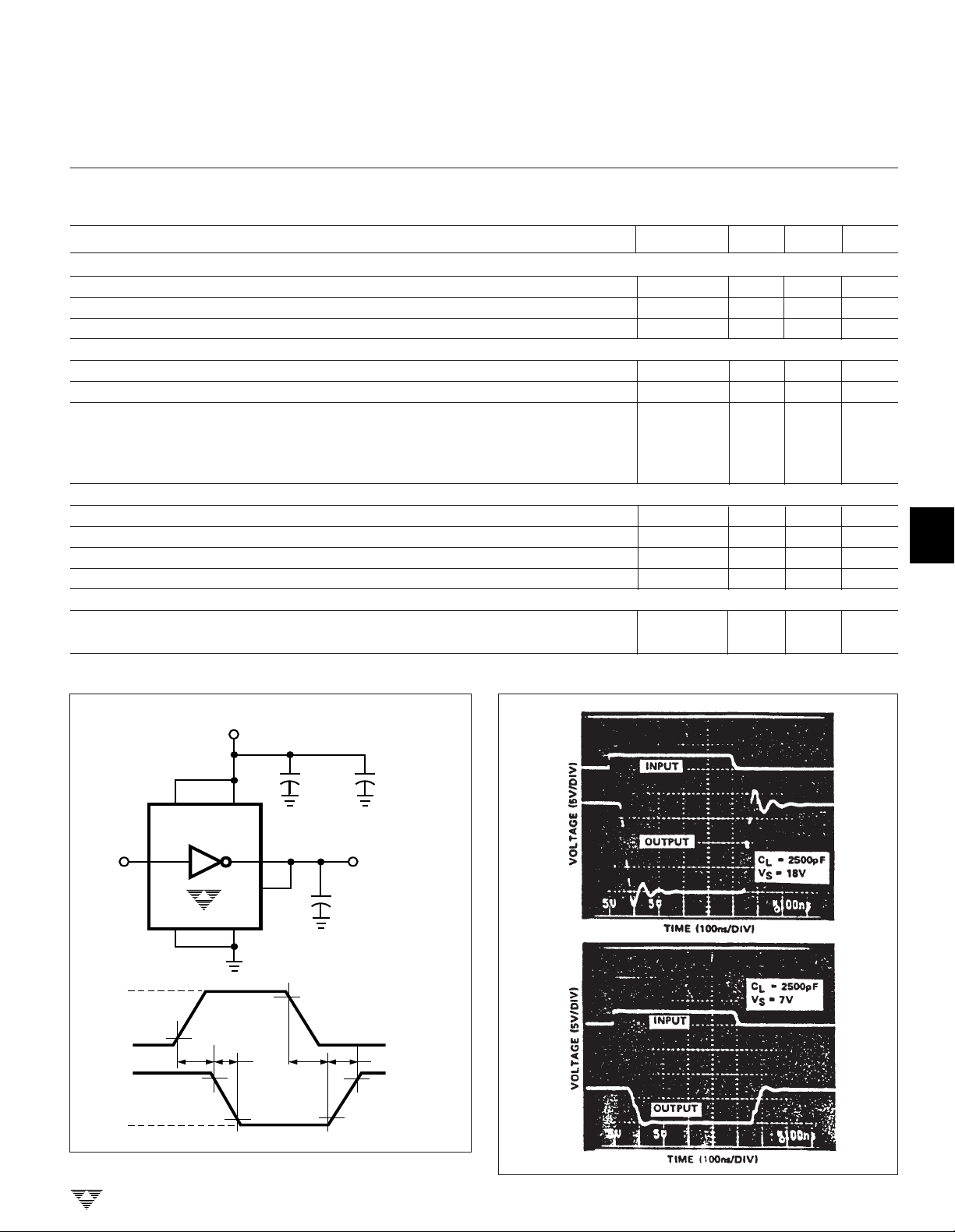
SWITCHING SPEED
VDD = 18V
2
3
4
5
18
INPUT
INPUT
OUTPUT
26
7
TC429
45
INPUT: 100 kHz, square wave
t
RISE
+5V
10%
0V
18V
0V
Figure 1. Inverting Driver Switching Time Test Circuit
TELCOM SEMICONDUCTOR, INC.
t
D1
90% 90%
t
90%
t
D2
F
0.1 µF 1 µF
OUTPUT
C
= 2500 pF
L
= t
10%10%
FALL
t
R
≤ 10 nsec
6
7
8
4-177
 Loading...