

TelCom Semiconductor Inc TC38C43CPD, TC38C43CPA, TC38C43COE, TC28C43EPD, TC28C43EPA Datasheet
...
BiCMOS CURRENT MODE PWM CONTROLLERS
TC18C43
1
TC28C43
TC38C43
FEATURES
■ Low Power BiCMOS Design
■ Tough CMOS
■ Low Supply Current .............1.0mA Typ @ 100kHz
■ Wide Supply Voltage Operation .............. 8V to 15V
■ Latch-Up Immunity ................... 500mA on Outputs
■ Input Will Withstand Negative Inputs to – 5 Volts
■ High Output Drive .................................... 0.7A Peak
■ 2 kV ESD Protection
■ Current Mode Control
■ Fast Rise/Fall Time (Max)...........60nsec @ 1000pF
■ High Frequency Operation ..........................500kHz
■ Clock Ramp Reset Current .................2.5mA ±10%
■ Low Propagation Delay Current Amp
to Output ............................................ 140nsec Typ.
■ Pin Compatible with UC3843
TM
Construction
(1.2A on 14-Pin and 16-Pin Versions)
ORDERING INFORMATION
Part No. Package Temperature
TC18C43MJA 8-Pin CerDIP – 55°C to +125°C
TC18C43MJD 14-Pin CerDIP – 55°C to +125°C
TC28C43EOE 16-Pin SOIC (Wide) – 40°C to +85°C
TC28C43EPA 8-Pin Plastic DIP – 40°C to +85°C
TC28C43EPD 14-Pin Plastic DIP – 40°C to +85°C
TC38C43COE 16-Pin SOIC (Wide) 0°C to +70°C
TC38C43CPA 8-Pin Plastic DIP 0°C to +70°C
TC38C43CPD 14-Pin Plastic DIP 0°C to +70°C
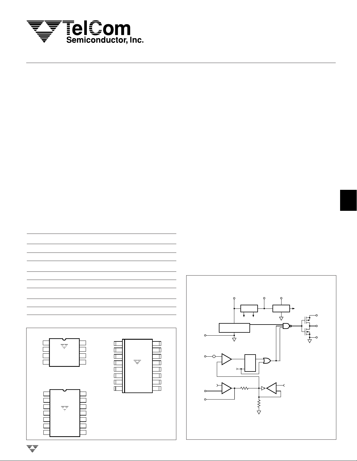
PIN CONFIGURATIONS
16-Pin SOIC (Wide)8-Pin Plastic DIP
1
CMPTR
2
V
I
SENSE
RT/C
FB
TC18CMJA
TC28CEPA
3
TC38CCPA
4
T
14-Pin Plastic DIP
CMPTR
114
213
NC
312
V
FB
411
I
SENSE
RT/C
NC
NC
TC18CMJD
TC28CEPD
510
TC38CCPD
69
78
T
TELCOM SEMICONDUCTOR, INC.
8
7
6
5
V
REF
V
IN
OUTPUT
GND
V
REF
NC
V
IN
V
DD
OUTPUT
GND
POWER
GND
NC
1
NC
2
CMPTR
3
V
4
FB
I
5
SENSE
RT/C
6
T
NC
7
NC
TC28CCOE
TC38CEOE
16
NC
15
V
REF
14
V
IN
13
V
DD
12
OUTPUT
11
GND
POWER
10
GND
98
NC
GENERAL DESCRIPTION
The TC38C43 is a current mode BiCMOS PWM control
IC. With a low 1.0 mA supply current along with high drive
current (0.7A peak) it provides a low cost solution for a PWM
that operates to 500 kHz and directly drives MOSFETs up to
HEX 3 size.
Performance of the oscillator and current sense amplifier have been greatly improved over previous bipolar versions. Voltage and temperature stability have been improved by a factor of 3. Noise immunity (PSRR) has also
been improved.
The TC38C43 is pin compatible with the earlier bipolar
version so that designers can easily update older designs.
Improvements have been added, though. For example,
clock ramp reset current is specified at 2.5mA (±10%) for
accurate dead time control. A few component values must
be changed (RT & CT) to use the TC38C43 in existing bipolar
designs.
The 14-pin DIP and 16-pin SOIC versions have separate and internally isolated grounds, and are rated for higher
output current (1.2A). These separate grounds allow for
‘bootstrap’ operation of the PWM to further improve efficiency.
FUNCTIONAL BLOCK DIAGRAM
R/TC
V
REF
S
R
V
UV GOOD
Q
REF
14
R
T
7
OSC
LIMIT BUFFER
1.4V
+
–
CLK
11
V
10
OUTPUT
8
POWER
GROUND
PIN NUMBERS FOR
14-PIN DIP
TC38C43-7 10/21/96
DD
4-93
ANALOG
GND
SENSE
V
COMP
V
IN
12
2.5V 1.4V
UNDER VOLTAGE
SECTION
9
PWM COMPARATOR
0.4V
+
– +
5
–
CLK
ERROR AMP
2.5V
+
FB
–
3
1
2R
2
3
4
5
6
7
8
TC18C43
TC28C43
TC38C43
BiCMOS CURRENT MODE
PWM CONTROLLERS
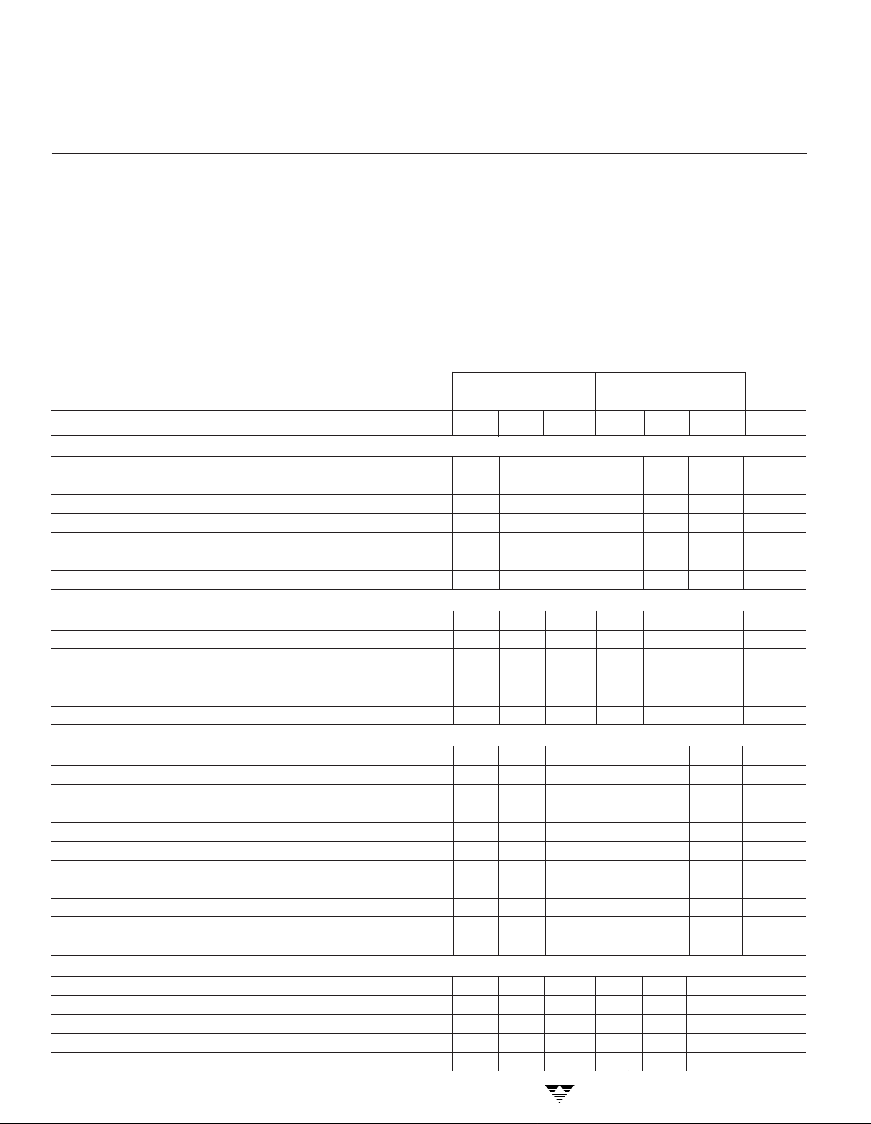
ABSOLUTE MAXIMUM RATINGS*
Supply Voltage ............................................................18V
Maximum Chip Temperature................................... 150°C
Storage Temperature ............................– 65°C to +150°C
Lead Temperature (Soldering, 10 sec) .................+300°C
Package Thermal Resistance
CerDip R
CerDip R
................................................ 150°C/W
θJ-A
.................................................. 55°C/W
θJ-C
PDIP R
PDIP R
SOIC R
SOIC R
Operating Temperature
18C4x ...................................... – 55C° ≤ TA ≤ +125°C
28C4x ........................................ – 40C° ≤ TA ≤ +85°C
38C4x ............................................. 0C° ≤ TA ≤ +70°C
................................................... 125°C/W
θJ-A
..................................................... 45°C/W
θJ-C
................................................... 250°C/W
θJ-A
..................................................... 75°C/W
θJ-C
ELECTRICAL CHARACTERISTICS unless otherwise stated, these specifications apply over specific
temperature range. VIN = V
Parameter Test Conditions Min Typ Max Min Typ Max Units
Reference Section
Output Voltage TA = 25°C, IO = 1mA 4.9 5 5.1 4.90 5 5.10 V
Line Regulation 9.5V ≤ V
Load Regulation 1mA ≤ lO ≤ 11mA — ±5 ±15 — ±3 ±10 mV
Temp Stability (Note 1) — ±0.25 ±0.5 — ±0.25 ±0.5 mV/°C
Output Noise Voltage 10Hz ≤ f ≤ 10 kHz,TA = 25°C (Note 1) — 100 — — 100 — µV(rms)
Long Term Stability TA = 125°C, 1000 Hrs. (Note 1) — ±0.5 — — ±0.5 — %
Output Short Circuit -20 -50 -100 -30 -50 -100 mA
Oscillator Section
Initial Accuracy TA = 25°C (Note 4) 90 100 110 93.8 100 106.5 kHz
Voltage Stability 9.5V ≤ VIN ≤ 15V — ±0.2 ±0.3 — ±0.2 ±0.3 %
Temp Stability T
Clock Ramp Reset RT/CT Pin at 4V 2.25 2.5 2.75 2.25 2.5 2.75 mA
Amplitude RT/CT Pin Peak to Peak 2.45 2.65 2.85 2.45 2.65 2.85 V
Maximum Freq Note 1 1 — — 1 — — MHz
Error Amp Section
Input Offset Voltage V
Input Bias Current (Note 1) — ±0.3 ±2—±0.3 ±2nA
A
VOL
Gain Bandwidth Product (Note 1) 650 750 — 650 750 — kHz
PSRR 9.5V ≤ VIN ≤ 15V 80 100 — 80 100 — dB
Output Sink Current VFB = 2.7V, V
Output Source Current VFB = 2.3V, V
V
High VFB = 2.3V, RL = 10k to Ground 5.65 6 6.5 5.65 6 6.5 V
OUT
V
Low VFB = 2.7V, RL = 10k to V
OUT
Rise Response Note 1 — 5 7 — 5 7 µsec
Fall Response Note 1 — 3 5 — 3 5 µsec
Current Sense Section
Gain Ratio Notes 2 & 3 2.8 2.9 3.1 2.8 2.9 3.1 V/V
Maximum Input Signal V
PSRR 9.5V ≤ VIN ≤ 15V (Notes 1, 2 & 5) 70 80 — 70 80 — dB
Input Bias Current Note 1 — ±0.3 ± 2—±0.3 ±2nA
Delay to Output V(I
= 15V; RT = 71 kΩ; CT = 150 pF.
DD
TC18C43
TC28C43 TC38C43
≤ 15V, IO = 1mA — ±3 ±10 — ±3 ±10 mV
IN
≤ TA ≤ T
MIN
= 2.5V — ±15 ±50 — ±15 ±50 mV
(CMPTR)
2V ≤ VO ≤ 4V 70 90 — 70 90 — dB
(CMPTR)
= 5V (Note 2) 0.85 0.95 1.05 0.85 0.95 1.05 V
= 1V (Note 1); Figure 3 — 140 160 — 140 150 nsec
SENSE)
(Note 1); Figure 2 — ±0.01 ±0.05 — ±0.01 ±0.03 %/°C
MAX
= 1.1V (Note 1) 1.2 1.5 — 1.5 1.7 — mA
(CMPTR)
= 5V (Note 1) 3 3.4 — 3.9 4.2 — mA
(CMPTR)
REF
0.1 0.7 1.1 0.1 0.7 1.1 V
4-94
TELCOM SEMICONDUCTOR, INC.
)
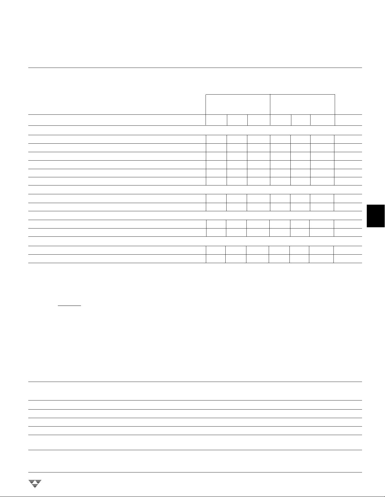
BiCMOS CURRENT MODE
PWM CONTROLLERS
TC18C43
TC28C43
TC38C43
ELECTRICAL CHARACTERISTICS (Cont): unless otherwise stated, these specifications apply over specified
temperature range. VIN = V
Parameter Test Conditions Min Typ Max Min Typ Max Units
Output Section
R
DS (ON) I
R
DS (ON) I
Rise Time CL = 1nF (Note 1) — 40 60 — 35 60 nsec
Fall Time CL = 1nF (Note 1) — 30 60 — 30 40 nsec
Cross Conduction In Coulombs (Note 1) — 6.5 — — 6.5 — nC
VDD Ma Note 1 — — 18 — — 18 V
Undervoltage Lockout Section
Start Threshold x8C43 7.9 8.4 8.8 7.9 8.4 8.8 V
Undervoltage Threshold x8C43 7.2 7.6 7.9 7.2 7.6 7.9 V
PWM Section
Maximum Duty Cycle x8C43 (Note 1) 95 97 100 95 97 100 %
Minimum Duty Cycle 0 0 %
Supply Current
Start Up TA = 25°C, VIN < VUV; Figure 1 50 170 300 50 170 300 µA
Operating VFB = V(I
NOTES: 1. These parameters, although guaranteed over the
TelCom Semiconductor reserves the right to make changes in the circuitry or specifications detailed in this manual at any time without notice. Minimums
and maximums are guaranteed. All other specifications are intended as guidelines only. TelCom Semiconductor assumes no responsibility for the use of
any circuits described herein and makes no representations that they are free from patent infringement.
*Static-sensitive device. Unused devices must be stored in conductive material. Protect devices from static discharge and static fields. Stresses above
those listed under Absolute Maximum Ratings may cause permanent damage to the device. These are stress ratings only and functional operation of
the device at these or any other conditions above those indicated in the operational sections of the specifications is not implied. Exposure to Absolute
Maximum Rating Conditions for extended periods may affect device reliability.
recommended operating conditions, are not tested in
production.
2. Parameter measured at trip point of latch.
3. Gain ratio is defined as:
∆V
COMP
∆V(I
SENSE
= 15V; RT = 71 kΩ; CT = 150 pF.
DD
TC18C4X
TC28C4X TC38C4X
= 20mA — 7 15 — 7 15 Ω
SINK
= 20mA — 11 20 — 11 15 Ω
SOURCE
) = 0V; Figure 4 1 2 1 1.5 mA
SENSE
where 0 ≤ V(I
4. Output frequency equals oscillator frequency for the
x8C43.
5. PSRR of V
combination.
) ≤ 0.8V
SENSE
, Error Amp and PWM Comparator
REF
1
2
3
4
5
6
PIN DESCRIPTION
Pin No. Pin No Pin No
8-Pin 14-Pin 16-Pin Symbol Description
2 1 NC No Connection
4 2 NC No Connection
1 1 3 CMPTR Compensation of the feedback loop response.
234 VFBFeedback of voltage to error amplifier to regulate voltage.
355I
4 7 6 R
TELCOM SEMICONDUCTOR, INC.
SENSE
/C
T
T
For sensing pass transistor current and terminate drive when current
limit threshold is reached at this pin.
Capacitor and resistor input to set oscillator frequency of this PWM
controller. The resistor is connected from V
The capacitor is connected from RT/CT to ANALOG GND.
output to RT/C
REF
7
T.
8
4-95

BiCMOS CURRENT MODE
TC18C43
TC28C43
TC38C43
PIN DESCRIPTION (Cont.)
Pin No. Pin No Pin No
8-Pin 14-Pin 16-Pin Symbol Description
6 7 NC No Connection
13 8 NC No Connection
9 NC No Connection
8 10 POWER GROUND Ground return of output driver.
5 9 11 ANALOG GND For all the low level analog signal returns.
6 10 12 OUTPUT Output to drive switching transistor gate input.
11 13 V
71214 V
81415 V
16 NC No Connection.
DD
IN
REF
REFERENCE SECTION
The reference is a zener-based design with a buffer
amplifier to drive the output. It is unstable with capacitances
between 0.01µF and 3.3µF. In a normal application a 4.7µF
is used. In some lower noise layouts the capacitor can be
eliminated entirely.
The reference is active as soon as the 38C4x has
power supplied. This is different than its bipolar counterparts, in that the bipolar reference comes on only after the IC
has come out of its under voltage mode. Thus, on the 38C4x,
the reference pin can not be used as a reset function such
as on a soft start circuit.
OSCILLATOR SECTION
The oscillator frequency is set by the combination of a
resistor from the reference to the RT/CT pin and by a
capacitor from this pin to ground. The oscillator is designed
to have ramp amplitude from 0.15 to 2.5 volts. This is
approximate, as over shoot on the oscillator comparator
causes the ramp amplitude to increase with frequency due
to comparator delay. Minimum values for CT and RT are
33pF and 1kΩ respectively. Maximum values are dependent on leakage currents in the capacitor, not on the input
currents to the RT/CT pin.
Supply power input terminal for the output drivers.
Voltage bias supply of all PWM Controller circuit functions.
Reference: 5.0 volt output.
fO ≈ 1 (RT in Ohms and CT in Farads)
RT C
T
The value of RT affects the discharge current and the
upper and lower comparators each have delays. As RT gets
smaller and as the frequency of operation gets higher, the
above equation is no longer valid.
14
R
T
C
T
PIN NUMBERS FOR 14-PIN DIP
PWM CONTROLLERS
V
(5V)
REF
7
RT/C
T
9
GND
FREQUENCY OF OPERATION
The frequency of oscillation for the TC38C43 is controlled by a resistor to V
(CT). V
supplies current through the resistor and charges
REF
the capacitor until its voltage reaches the threshold of the
upper comparator (≈2.5V). A 2.5mA current is then applied
to the capacitor to discharge it to near ground (≈0.15V). The
discharge current is then shut off and the cycle repeats. An
approximate equation for the frequency of operation is:
4-96
(RT) and a capacitor to ground
REF
TELCOM SEMICONDUCTOR, INC.

BiCMOS CURRENT MODE
PWM CONTROLLERS
TC18C43
TC28C43
TC38C43
1
Dead Time
The value of RT has an effect on the discharge rate but
the primary consideration is the value of CT. The time
required to discharge the capacitor is approximately 1000
CT.
UNDERVOLTAGE LOCKOUT RANGE
V
IN
I
S
7.6V
TCx8C43
8.4 V
V
DD
TCx8C43
VON = 8.4V
V
= 7.6V
OFF
1mA
170µA
Undervoltage Lockout Range
The TCx8C43 PWM Controller is used where wide
ranges of input voltage is not required. The range from
starting Vin voltage threshold to under voltage threshold is
approximately 9.5% of the starting voltage. The typical startup voltage is 8.4V and dropout voltage is 7.6V. This range
is used most in DC-to-DC converter applications.
Duty Cycle Limit
The TCx8C43 PWM Controller has a duty cycle limit
maximum of 99%. The oscillator is running at the same
frequency as the output.
CURRENT SENSE CIRCUIT
+
PWM
COMPARATOR
+
–
2R
R
LIMIT BUFFER
+
–
1.4V
I
R
R
S
SENSE
C
GND
5
9
0.4V
–
ERROR AMP
Current is sensed through voltage drop across resistor
RS. A small RC filter may be required to suppress switching
transient. This voltage enters PWM Controller at I
SENSE
pin 5. A voltage of 0.4 V is added before this is fed into PWM
Comparator (+) input. The PWM Comparator (–) input
senses the voltage feedback error amp output with a limit
buffer that limits this voltage to 1.4V maximum. This limit
buffer limits the peak current across RS to a maximum of
0.95V. In normal operation, the error amplifier controls the
current limit threshold.
SHUTDOWN METHODS
TCx38C43
14
V
REF
5k
SHUTDOWN
I
SENSE
5.1k
SHUTDOWN
TO CURRENT
SENSE RESISTOR
5
Shutdown can be accomplished by either pulling I
TCx38C43
1
CMPTR
ANALOG
GND
9
SENSE
above 1 volt or pulling CMPTR, pin 1 to GND. This will set the
PWM latch so that the output will remain low until the next
clock pulse after the shutdown condition is removed.
BENCH TEST OPERATIONAL SIMULATION
The timing ramp (RT/CT) is buffered by the emitter
fullpower and fed back to the I
simulates the dI/dT current ramp which would flow through
the primary of the transformer. The output voltage of the
power supply is simulated by feeding some of the reference
voltage into VFB. The combination of the two levels determined the operating characteristics of the current mode
controller.
input. This ramp
SENSE
,
2
3
4
5
6
7
PEAK CURRENT (IS) FORMULA:
0.95V
IS =
R
S
TELCOM SEMICONDUCTOR, INC.
8
4-97

TC18C43
TC28C43
TC38C43
10k
5k
10k
5k
Q1
R
2N2222
OR EQUIV
I
RAMP
C
BENCH TEST OPERATIONAL SIMULATION
T
1
CMPTR
V
REF
100k
2
3
4
V
FB
I
SENSE
RT/C
T
V
IN
OUTPUT
GND
T
BiCMOS CURRENT MODE
PWM CONTROLLERS
8
4.7µF
7
6
5
1µF
RL = 1k, 1W
V
DD
GND
(15V)
TYPICAL CHARACTERISTICS
Start Current vs. Temperature
150
VIN = V
145
140
135
130
(µA)
125
120
START
I
115
110
105
100
START
MAX TYP
MIN TYP
–40 –20 0 20 40 60 80 100120140–60
TEMPERATURE (°C)
Oscillator Frequency Changes
vs. Temperature
101
VIN = 15V
100
99
98
FREQUENCY (kHz)
97
96
–60 –40–20 0 20 406080 100120 140
TEMPERATURE (°C)
I
150
140
130
120
110
DELAY (nse c)
100
SENSE
–55900 255070125
to Out Delay
TEMPERATURE (°C)
4-98
TELCOM SEMICONDUCTOR, INC.

BiCMOS CURRENT MODE
PWM CONTROLLERS
TYPICAL CHARACTERISTICS (Cont.)
TC18C43
TC28C43
TC38C43
1
IDD vs. Temperature
2.0
VIN = 15V
f = 100kHz
1.8
1.6
(mA)
DD
1.4
I
1.2
1.0
–60–40–20 0 20 40 60 80 100120140
1000
800
600
D
400
P (mW)
TEMPERATURE (°C)
PDIP
SLOPE = – 8mW/°C
CerDIP
SLOPE = – 6.4mW/°C
10 nF
T
1nF
C
100pF
Frequency of Operation
10 kHz
100kHz 1 MHz
FREQUENCY
RT = 10 k
RT = 22 k
RT = 47 k
RT = 100 k
10nF
T
1nF
C
100pF
100nsec
Dead Time vs. C
1 µsec 10µsec
DISCHARGE TIME
T
2
3
4
5
200
SOIC
SLOPE = – 4mW/°C
0
25 50 75 100 125 150
AMBIENT TEMPERATURE (°C)
6
7
8
TELCOM SEMICONDUCTOR, INC.
4-99
 Loading...