

TelCom Semiconductor Inc TC35C25CPE, TC35C25COE, TC25C25EPE, TC25C25EOE Datasheet
BICMOS PWM CONTROLLERS
1
TC25C25
TC35C25
FEATURES
■ Low Power BICMOS Construction
■ Low Supply Current at 20 kHz ...............1.0mA Typ
■ Latch-Up Immunity ................. >500mA on Outputs
■ Below Rail Input Protection ..............................– 5V
■ High Output Drive ................................500mA Peak
■ Fast Rise/Fall Time ..................... 50nsec @ 1000pF
■ High Frequency Operation .................. Up to 1MHz
■ Tri-state Sync Pin for Easy Parallel Operation
■ Under Voltage Hysteresis Guaranteed
■ Shutdown Pin Available
■ Double-Ended
■ Soft Start, With Small Cap
■ Low Prop Delay Shutdown to
Output ................................................. 140nsec Typ.
ORDERING INFORMATION
Part No. Configuration Pkg./Temperature
TC25C25EOE Non-Inverting 16-Pin SOIC (Wide)
– 40°C to +85°C
TC25C25EPE Non-Inverting
TC35C25COE Non-Inverting 16-Pin SOIC (Wide)
TC35C25CPE Non-Inverting
16-Pin Plastic DIP (Narrow)
– 40°C to +85°C
0°C to +70°C
16-Pin Plastic DIP (Narrow)
0°C to +70°C
GENERAL DESCRIPTION
The TC35C25 family of PWM controllers are CMOS
implementations of the industry standard 3525 voltage
mode SMPS ICs.
These second generation CMOS devices employ
TelCom Semiconductors' Tough BiCMOS process for
latch-up proof operation. They offer much lower power
consumption than any of their previous CMOS or bipolar
counterparts.
These controllers have separate supply pins for the
control and output sections of the circuit. This allows "bootstrap" operation. The CMOS output stage allows the output
voltage to swing to within 25mV of either rail.
Other improved features include tighter hysteresis and
undervoltage start-up specifications over temperature, and
very low input bias current on all inputs.
2
3
4
5
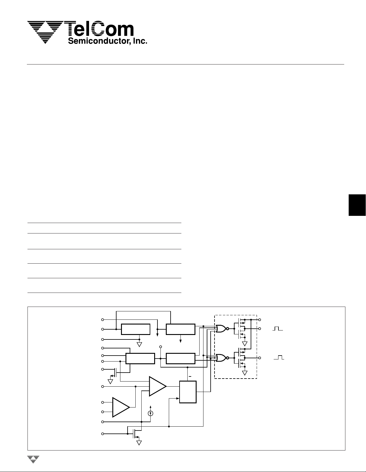
FUNCTIONAL BLOCK DIAGRAM
16
V
REF
15
+
V
IN
12
GND
3
SYNC
6
R
T
5
C
T
7
DISCH
9
COMP
1
–
IN
IN
SOFT
START
SHUTDOWN
ERROR
2
+
AMP
8
10
TELCOM SEMICONDUCTOR, INC.
UNDER
VOLTAGE
OSC
+4V REF
OSC OUT
CMPTR
+6V
50µA
REFERENCE
REGULATOR
4
+6V
FLIP
FLOP
S
R
PWM
LATCH
35C25
R
13
V
DD
11
A
14
B
6
7
8
TC25/35C25-2 10/1/96
4-111
TC25C25
TC35C25
BICMOS PWM CONTROLLERS
ABSOLUTE MAXIMUM RATINGS*
Supply Voltage ............................................................18V
Maximum Chip Temperature................................... 150°C
Storage Temperature ............................– 65°C to +150°C
Lead Temperature (10 sec)..................................... 300°C
Package Thermal Resistance
PDIP R
PDIP R
SOIC R
SOIC R
..................................................................... 125°C/W
θJ-A
........................................................................45°C/W
θJ-C
..................................................................... 250°C/W
θJ-A
........................................................................75°C/W
θJ-A
ELECTRICAL CHARACTERISTICS: Unless otherwise stated, these specifications apply for – 40°C < T
Operating Temperature
25C2x ........................................– 40°C ≤ TA ≤ +85°C
35C2x .............................................0°C ≤ TA ≤ +70°C
*Static-sensitive device. Unused devices must be stored in conductive
material. Protect devices from static discharge and static fields. Stresses
above those listed under Absolute Maximum Ratings may cause permanent damage to the device. These are stress ratings only and functional
operation of the device at these or any other conditions above those
indicated in the operational sections of the specifications is not implied.
<
A
+85°C for the TC25C25Exx; and 0°C <TA < +70°C for the TC35C25Cxx;
VIN and VDD = 16V; RT = 3.7kΩ; CT = 1000pF; RD = 760Ω.
Parameter Test Conditions Min Typ Max Units
Reference Section
Output Voltage TJ = 25°C, IO = 1mA 3.9 4 4.1 V
Line Regulation V
Load Regulation II = 1mA to mA — ±4 ±15 mV
Temp Coefficient Note 1 — ±0.01 ±0.4 mV/°C
V
REF
Long Term Drift TJ = 25°C, (Note 1) — ±50 — mV/
Short Circuit V
Output Noise TJ = 25°C, 10 Hz ≤ f ≥ 10 kHz, (Note 1) — 21 — µV(rms)
= 8V to 18V — ±4 ±10 mV
IN
Worst Case 3.85 4 4.15 V
1000Hrs
to GND 20 40 70 mA
REF
Oscillator Section
Initial Accuracy TJ = 25°C, at 97 kHz — ±2 ±3%
Voltage Coefficient VIN = 8V to 18V — ±0.01 ±0.1 %/V
Temp Coefficient Note 1 — ±
OSC Ramp Amplitude 2.9 3.2 3.4 V
Reset Switch R
Clock Amplitude f
Clock Min Width T
Sync Threshold RT Pin Tied to V
Sync Input Current Sync Voltage = 4V, V(RT) = 4V — — ±1 µA
Min Sync Pulse Width TJ = 25°C, Sync Amplitude = 5V, (Note 1) — 130 175 nsec
Max OSC Freq RT = 1Ω, CT = 100pF, RD = 0Ω, (Note 1) 1.0 — — MHz
DS (ON)
TJ = 25°C305060Ω
= 100kHz, RL = 1MΩ, (Note 1) 4.9 5.5 6.7 V
osc
= 25°C, RD = 0Ω, (Note 1) — 170 200 nsec
J
CT = 100pF, RT = 1Ω
Pin at GND 1.8 2.2 2.8 V
REF, CT
0.025
±0.06 %/°C
Error Amplifier Section (VCM = 2.5V)
Input Offset Voltage — ±5 ±15 mV
Input Bias Current TJ = 25°C—±50 ±200 pA
Input Offset Current TJ = 25°C—±25 ±100 pA
DC Open Loop Gain RL = 100kΩ 70 85 — dB
Gain Bandwidth Product Note 1 0.7 0.9 1.2 MHz
Output Low Level RL = 100kΩ (N Channel) — 10 20 mV
Output High Level RL = 100kΩ (NPN) 4.9 5.4 5.9 V
CMRR VCM = 0.5 to 4.7V 60 75 — dB
4-112
TELCOM SEMICONDUCTOR, INC.
BICMOS PWM CONTROLLERS
1
TC25C25
TC35C25
ELECTRICAL CHARACTERISTICS: Unless otherwise stated, these specifications apply for – 40°C < T
+85°C for the TC25C25Exx; and 0°C <TA < +70°C for the TC35C25Cxx;
VIN and VDD = 16V; RT = 3.7kΩ; CT = 1000 pF; RD = 760 Ω.
Parameter Test Conditions Min Typ Max Units
Supply Voltage Rejection V
Slew Rate C
Threshold Hysteresis 0.6 0.8 1 V
Total Standby Current
Supply Current — 1.2 2.5 mA
Start-Up Current — 250 350 µA
PWM Comparator
Min. Duty Cycle Note 1, TJ = 25°C——0%
Max Duty Cycle TJ = 25°C, f
Input Threshold V(CT) = 0.6V 0.5 0.6 0.7 V
Input Threshold V(CT) = 3.6V 3.4 3.6 3.7 V
Input Bias Current Note 1, TJ = 25°C——±1µA
Soft Start Section
Soft Start Current V
Soft Start Voltage V
Shutdown Input Current V
Min Shutdown Pulse Width V
Shutdown Delay V
Shutdown Threshold 1.5 2.4 3 V
Output Drivers (each output)
Output Low Level RDS (ON) I
Output High Level RDS (ON) I
Rise Time CL = 1nF, (Note 1) — 55 80 nsec
Fall Time CL = 1nF, (Note 1) — 40 65 nsec
Power Supply
Supply Current f
UV Lockout Threshold 6.45 7 7.3 V
UV Lockout Hysteresis 1.7 2.2 2.5 V
Start-up Current — 75 200 µA
= 8V to 18V 90 120 — dB
IN
= 50pF, ACL = 1 — 1 — V/µsec
LOAD
V(EA+) = 1V to 3V Pulse, (Note 1) — — —
= 100kHz, (Note 1) 45 49 — %
OSC
SHUTDOWN
SHUTDOWN
SHUTDOWN
SHUTDOWN
SHUTDOWN
SINK
SOURCE
OSC
= 0V 30 46 75 µA
= 3V — 30 100 mV
= 3V — ±1 ±100 nA
= 5V, (Note 1) — 20 40 nsec
= 5V, (Note 1) 130 140 220 nsec
= 20mA — 13 25 Ω
= 20mA — 20 35 Ω
= 100kHz — 2 3 mA
<
A
2
3
4
5
6
NOTE: 1. Not Tested.
TelCom Semiconductor reserves the right to make changes in the circuitry or specifications detailed in this manual at any time without notice. Minimums
and maximums are guaranteed. All other specifications are intended as guidelines only. TelCom Semiconductor assumes no responsibility for the use of
any circuits described herein and makes no representations that they are free from patent infringement.
TELCOM SEMICONDUCTOR, INC.
4-113
7
8
 Loading...