

BICMOS PWM CONTROLLERS
1
TC25C25
TC35C25
FEATURES
■ Low Power BICMOS Construction
■ Low Supply Current at 20 kHz ...............1.0mA Typ
■ Latch-Up Immunity ................. >500mA on Outputs
■ Below Rail Input Protection ..............................– 5V
■ High Output Drive ................................500mA Peak
■ Fast Rise/Fall Time ..................... 50nsec @ 1000pF
■ High Frequency Operation .................. Up to 1MHz
■ Tri-state Sync Pin for Easy Parallel Operation
■ Under Voltage Hysteresis Guaranteed
■ Shutdown Pin Available
■ Double-Ended
■ Soft Start, With Small Cap
■ Low Prop Delay Shutdown to
Output ................................................. 140nsec Typ.
ORDERING INFORMATION
Part No. Configuration Pkg./Temperature
TC25C25EOE Non-Inverting 16-Pin SOIC (Wide)
– 40°C to +85°C
TC25C25EPE Non-Inverting
TC35C25COE Non-Inverting 16-Pin SOIC (Wide)
TC35C25CPE Non-Inverting
16-Pin Plastic DIP (Narrow)
– 40°C to +85°C
0°C to +70°C
16-Pin Plastic DIP (Narrow)
0°C to +70°C
GENERAL DESCRIPTION
The TC35C25 family of PWM controllers are CMOS
implementations of the industry standard 3525 voltage
mode SMPS ICs.
These second generation CMOS devices employ
TelCom Semiconductors' Tough BiCMOS process for
latch-up proof operation. They offer much lower power
consumption than any of their previous CMOS or bipolar
counterparts.
These controllers have separate supply pins for the
control and output sections of the circuit. This allows "bootstrap" operation. The CMOS output stage allows the output
voltage to swing to within 25mV of either rail.
Other improved features include tighter hysteresis and
undervoltage start-up specifications over temperature, and
very low input bias current on all inputs.
2
3
4
5
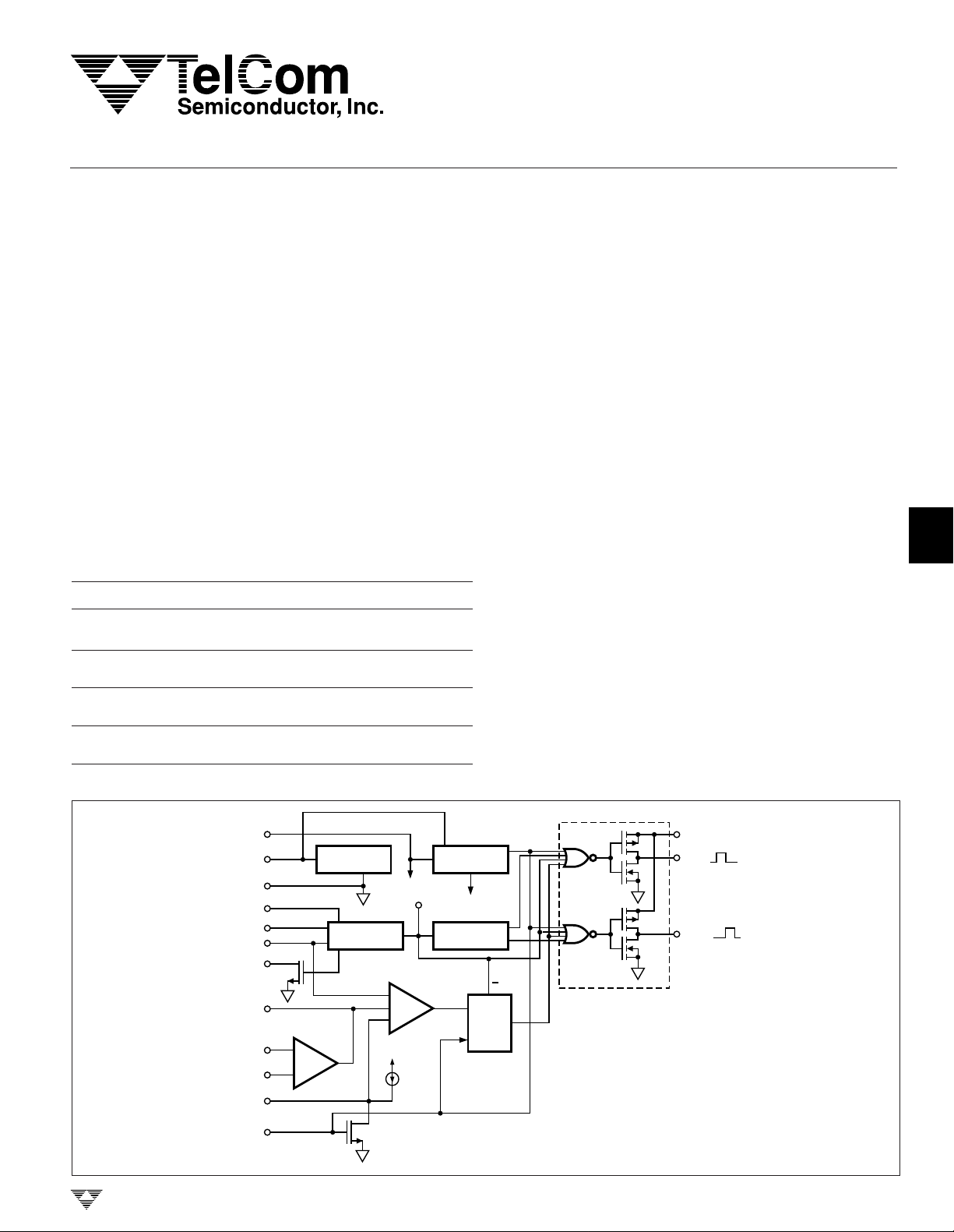
FUNCTIONAL BLOCK DIAGRAM
16
V
REF
15
+
V
IN
12
GND
3
SYNC
6
R
T
5
C
T
7
DISCH
9
COMP
1
–
IN
IN
SOFT
START
SHUTDOWN
ERROR
2
+
AMP
8
10
TELCOM SEMICONDUCTOR, INC.
UNDER
VOLTAGE
OSC
+4V REF
OSC OUT
CMPTR
+6V
50µA
REFERENCE
REGULATOR
4
+6V
FLIP
FLOP
S
R
PWM
LATCH
35C25
R
13
V
DD
11
A
14
B
6
7
8
TC25/35C25-2 10/1/96
4-111
TC25C25
TC35C25
BICMOS PWM CONTROLLERS
ABSOLUTE MAXIMUM RATINGS*
Supply Voltage ............................................................18V
Maximum Chip Temperature................................... 150°C
Storage Temperature ............................– 65°C to +150°C
Lead Temperature (10 sec)..................................... 300°C
Package Thermal Resistance
PDIP R
PDIP R
SOIC R
SOIC R
..................................................................... 125°C/W
θJ-A
........................................................................45°C/W
θJ-C
..................................................................... 250°C/W
θJ-A
........................................................................75°C/W
θJ-A
ELECTRICAL CHARACTERISTICS: Unless otherwise stated, these specifications apply for – 40°C < T
Operating Temperature
25C2x ........................................– 40°C ≤ TA ≤ +85°C
35C2x .............................................0°C ≤ TA ≤ +70°C
*Static-sensitive device. Unused devices must be stored in conductive
material. Protect devices from static discharge and static fields. Stresses
above those listed under Absolute Maximum Ratings may cause permanent damage to the device. These are stress ratings only and functional
operation of the device at these or any other conditions above those
indicated in the operational sections of the specifications is not implied.
<
A
+85°C for the TC25C25Exx; and 0°C <TA < +70°C for the TC35C25Cxx;
VIN and VDD = 16V; RT = 3.7kΩ; CT = 1000pF; RD = 760Ω.
Parameter Test Conditions Min Typ Max Units
Reference Section
Output Voltage TJ = 25°C, IO = 1mA 3.9 4 4.1 V
Line Regulation V
Load Regulation II = 1mA to mA — ±4 ±15 mV
Temp Coefficient Note 1 — ±0.01 ±0.4 mV/°C
V
REF
Long Term Drift TJ = 25°C, (Note 1) — ±50 — mV/
Short Circuit V
Output Noise TJ = 25°C, 10 Hz ≤ f ≥ 10 kHz, (Note 1) — 21 — µV(rms)
= 8V to 18V — ±4 ±10 mV
IN
Worst Case 3.85 4 4.15 V
1000Hrs
to GND 20 40 70 mA
REF
Oscillator Section
Initial Accuracy TJ = 25°C, at 97 kHz — ±2 ±3%
Voltage Coefficient VIN = 8V to 18V — ±0.01 ±0.1 %/V
Temp Coefficient Note 1 — ±
OSC Ramp Amplitude 2.9 3.2 3.4 V
Reset Switch R
Clock Amplitude f
Clock Min Width T
Sync Threshold RT Pin Tied to V
Sync Input Current Sync Voltage = 4V, V(RT) = 4V — — ±1 µA
Min Sync Pulse Width TJ = 25°C, Sync Amplitude = 5V, (Note 1) — 130 175 nsec
Max OSC Freq RT = 1Ω, CT = 100pF, RD = 0Ω, (Note 1) 1.0 — — MHz
DS (ON)
TJ = 25°C305060Ω
= 100kHz, RL = 1MΩ, (Note 1) 4.9 5.5 6.7 V
osc
= 25°C, RD = 0Ω, (Note 1) — 170 200 nsec
J
CT = 100pF, RT = 1Ω
Pin at GND 1.8 2.2 2.8 V
REF, CT
0.025
±0.06 %/°C
Error Amplifier Section (VCM = 2.5V)
Input Offset Voltage — ±5 ±15 mV
Input Bias Current TJ = 25°C—±50 ±200 pA
Input Offset Current TJ = 25°C—±25 ±100 pA
DC Open Loop Gain RL = 100kΩ 70 85 — dB
Gain Bandwidth Product Note 1 0.7 0.9 1.2 MHz
Output Low Level RL = 100kΩ (N Channel) — 10 20 mV
Output High Level RL = 100kΩ (NPN) 4.9 5.4 5.9 V
CMRR VCM = 0.5 to 4.7V 60 75 — dB
4-112
TELCOM SEMICONDUCTOR, INC.
BICMOS PWM CONTROLLERS
1
TC25C25
TC35C25
ELECTRICAL CHARACTERISTICS: Unless otherwise stated, these specifications apply for – 40°C < T
+85°C for the TC25C25Exx; and 0°C <TA < +70°C for the TC35C25Cxx;
VIN and VDD = 16V; RT = 3.7kΩ; CT = 1000 pF; RD = 760 Ω.
Parameter Test Conditions Min Typ Max Units
Supply Voltage Rejection V
Slew Rate C
Threshold Hysteresis 0.6 0.8 1 V
Total Standby Current
Supply Current — 1.2 2.5 mA
Start-Up Current — 250 350 µA
PWM Comparator
Min. Duty Cycle Note 1, TJ = 25°C——0%
Max Duty Cycle TJ = 25°C, f
Input Threshold V(CT) = 0.6V 0.5 0.6 0.7 V
Input Threshold V(CT) = 3.6V 3.4 3.6 3.7 V
Input Bias Current Note 1, TJ = 25°C——±1µA
Soft Start Section
Soft Start Current V
Soft Start Voltage V
Shutdown Input Current V
Min Shutdown Pulse Width V
Shutdown Delay V
Shutdown Threshold 1.5 2.4 3 V
Output Drivers (each output)
Output Low Level RDS (ON) I
Output High Level RDS (ON) I
Rise Time CL = 1nF, (Note 1) — 55 80 nsec
Fall Time CL = 1nF, (Note 1) — 40 65 nsec
Power Supply
Supply Current f
UV Lockout Threshold 6.45 7 7.3 V
UV Lockout Hysteresis 1.7 2.2 2.5 V
Start-up Current — 75 200 µA
= 8V to 18V 90 120 — dB
IN
= 50pF, ACL = 1 — 1 — V/µsec
LOAD
V(EA+) = 1V to 3V Pulse, (Note 1) — — —
= 100kHz, (Note 1) 45 49 — %
OSC
SHUTDOWN
SHUTDOWN
SHUTDOWN
SHUTDOWN
SHUTDOWN
SINK
SOURCE
OSC
= 0V 30 46 75 µA
= 3V — 30 100 mV
= 3V — ±1 ±100 nA
= 5V, (Note 1) — 20 40 nsec
= 5V, (Note 1) 130 140 220 nsec
= 20mA — 13 25 Ω
= 20mA — 20 35 Ω
= 100kHz — 2 3 mA
<
A
2
3
4
5
6
NOTE: 1. Not Tested.
TelCom Semiconductor reserves the right to make changes in the circuitry or specifications detailed in this manual at any time without notice. Minimums
and maximums are guaranteed. All other specifications are intended as guidelines only. TelCom Semiconductor assumes no responsibility for the use of
any circuits described herein and makes no representations that they are free from patent infringement.
TELCOM SEMICONDUCTOR, INC.
4-113
7
8

TC25C25
TC35C25
PIN CONFIGURATION (DIP AND SOIC)
–
IN
1
+
IN
215
SYNC
OSC OUT
DISCHARGE
SOFT START
314
413
C
T
R
T
TC25C25EPE
TC35C25CPE
512
611
710
89
16
V
REF
+
V
IN
OUTPUT B
V
DD
GND
OUTPUT A
SHDN
CMPTR
IN
IN
SYNC
OSC OUT
C
R
DISCHARGE
SOFT START
BICMOS PWM CONTROLLERS
–
1
+
2
3
4
TC25C25EOE
TC35C25COE
5
T
6
T
7
8
16
15
14
13
12
11
10
9
V
REF
+
V
IN
OUTPUT B
V
DD
GND
OUTPUT A
SHDN
CMPTR
PIN DESCRIPTION
Pin No. Symbol Description
1IN
2IN
3 SYNC Input pin for PWM controller oscillator synchronization of two or more controllers from an
4 OSC OUT Pin for output of the internal oscillator. This signal can be used as a master oscillator to
5C
6R
7 DISCHARGE Pin for discharging the timing capacitor, C
8 SOFT START Pin for soft starting the power supply. A capacitor from this pin to GND pin 12 will limit
9 CMPTR Pin for compensation of the feedback loop response.
10 SHDN Pin for terminating both outputs of pins 11 and 14. This will shutdown the power supply
11 OUTPUT A Pin for output drive of phase A to drive push pull transistor A.
12 GND Pin for ground return for all inputs and output signals.
13 V
14 OUTPUT B Pin for output drive of phase B to drive push pull transistor B.
15 V
16 V
–
+
T
T
DD
+
IN
REF
Error Amplifier inverting input for output voltage reference input and amplifier gain set.
Error Amplifier, non-inverting input for output voltage feedback to regulate voltage.
external clock output or from another PWM controller oscillator output.
sync other oscillators to run at the same timing period.
Pin is the capacitor timing input to set oscillator frequency in conjunction with pin 6 RT timing
resistor.
Pin for timing resistor input to set oscillator frequency by setting the charge current into
capacitor CT of pin 5.
of pin 5. During discharging time period, PWM
T
controller output is disabled. This is called dead time. With a resistor between pin 7 and pin 5,
the dead time can be controlled.
duty cycle till capacitor is charged above error amplifier output.
outputs. A positive input with shutdown threshold of 2.4V is required for shutdown.
Pin for power supply input to operate the output drivers A and B.
Pin for voltage bias supply input for all PWM controller functions except output drive circuits.
Pin is the reference supply output voltage of 4.0 volts that may be used for any voltage
reference purposes such as a reference to control output voltage.
4-114
TELCOM SEMICONDUCTOR, INC.

BICMOS PWM CONTROLLERS
1
TC25C25
TC35C25
OUTPUT SECTION
The output stage of the TC35C25 is comprised of two
pairs of complimentary CMOS drivers operating in a pushpull mode. Each output is capable of sinking or sourcing
nearly 500mA of peak current. They are also capable of
absorbing just as much "kick-back" current without latching.
SOFT START
A soft restart recovery rate may be selected by placing
a capacitor from SOFT START (pin 8) to ground. The
calculation for the recovery timing is approximately 60 msec/
µF.
SOFT START will mediate the start-up from under
voltage recovery, power-on, or SHUTDOWN.
SHUTDOWN
There is a minimum delay, non-latching shutdown feature on the TC35C25 PWM controller. Both outputs may be
turned off by applying a positive voltage to SHUTDOWN (pin
10). Typical shutdown threshold is 2.4V. Returning the pin
back to ground will reinitialize the soft start cycle.
OSCILLATOR SECTION
A tri-state feature has been added to accommodate
systems which require multiple controllers to be run in a
"master/slave" configuration. The timing resistor pin (RT, pin
6) may be tied to V
in a high impedance state. This will allow the chip to be
clocked from an external source.
The sync output (OSC OUT, pin 4) of the TC35C25 can
drive several sync inputs configured in this manner.
to place the sync pin (SYNC, pin 3)
REF
OSCILLATOR SYNCHRONIZATION WITH
SEPARATE RC TIMER
Synchronization can also be done by having a separate
RC timing circuit on the slave oscillator that is slightly lower
frequency than the master oscillator. The sync input will not
be in a high impedance state so the number of slave
oscillators is limited. This method of synchronization is
useful when slave oscillator is located in a different location.
When a separate RC timer is used in the slave controller,
ground loop noise pickup in the oscillator is minimized.
6
R
T
R
T
5
C
C
T
6
R
R
T
5
C
C
T
TCx5C25
GND
T
12
V
REF
T
TCx5C25
GND
T
12
SLAVE TC > MASTER TC
OSC OUT
4
SYNC
MASTER
3
SLAVE
2
3
4
5
OSCILLATOR SYNCHRONIZATION
Synchronization of two TC35C25's can be done by
making one PWM Controller as the master oscillator to
synchronize the slave as follows:
6
R
T
R
T
5
C
T
6
5
TCx5C25
C
GND
T
V
R
REF
T
C
GND
T
OSC OUT
12
16
SYNC
TCx5C25
12
TELCOM SEMICONDUCTOR, INC.
MASTER
4
3
SLAVE
6
7
8
4-115

TC25C25
TC35C25
OSCILLATOR FREQUENCY AND OUTPUT DEAD TIME
BICMOS PWM CONTROLLERS
1/FO
V
DD
3V0.5V
I
CHARGE
3
SYNC
7
DISCH
5
R
D
C
T
The oscillator frequency (FO) =
T
is the charging duration of CT. One of the PWM
CHG
T
≈
CHG
1.5V
1
+ T
R
T
6
R
T
D
Controller output drivers is ON during charging of CT. TD is
the output dead time when both of the output drivers are
inactive. Resistor (RT) sets the Capacitor (CT) charging
current.
To choose an oscillator frequency (FO), first select the
period of dead time (TD) required. Calculate the capacitor
charge time (T
CHG
T
).
CHG
1 – FO x T
=
C
F
O
T
D
PIN 5
1.5V
+
–
+
V
IN
ON-TIME
(T
)
CHG
PIN 4
OUTPUT DEAD TIME (TD)
TO OUTPUT
SHUTDOWN
VON = 9.2V
V
= 7V
OFF
I
S
1mA
75µA
I
= STARTUP CURRENT
S
UNDERVOLTAGE LOCKOUT SECTION
3V
.5V
7V 9.2V
V
IN
Select a capacitor in the range of 100 pF to 1000 pF for
CT. See graph in Typical Characteristic Curve. Calculate
capacitor charging current (I
I
=
CHG
CT in Farads, T
in seconds, I
CHG
).
CHG
2.5 x C
T
CHG
T
in amperes, and
CHG
RT in ohms.
RT =
1.5
I
CHG
The resistor (RD) controls the period of dead time (TD).
During dead time this resistor (RD) current is the sum of the
CT discharge current and the I
current. The value for R
CHG
can range from >1Ω to <900Ω. Dead time increases when
RD is increased. See graph in Typical Characteristic Curve
for dead time resistor value.
4-116
The typical turn on threshold is 9.2V for operation of this
family of PWM Controllers. When supply voltage at pin 15
drops below 7V, after normal operation above 9.2V, lockout
occurs and both output drives to pin 11 and 14 are terminated.
D
TELCOM SEMICONDUCTOR, INC.

BICMOS PWM CONTROLLERS
BENCH TEST OPERATIONAL SIMULATION WAVEFORMS
0.5V
3V
PIN 2
VOLTAGE
DEAD TIME
C
T
PIN 5
OSC OUT
PIN 4
OUTPUT A
PIN 11
OUTPUT B
PIN 14
1000pF
MET
3.7k
5k
GND
0 to 1k
1
2
3
4
5
6
7
8
–
IN
+
IN
SYNC
OSC OUT
C
T
R
T
DISCH
SOFT
GND
V
REF
V
IN
OUT
B
V
DD
GND
OUT
A
SHDN
CMPTR
16
15
14
13
12
11
10
9
TC25C25
TC35C25
MET
V011
+
–
.1µf
16V
1
2
3
The 5k potentiometer sets a reference voltage at pin 2.
When ramp voltage of pin 5 reaches this reference voltage,
output drive pulse is active ON. Varying the discharge
resistor will vary the dead time. Increasing the discharge
resistor will effect an increase in the dead time.
TYPICAL CHARACTERISTICS
Supply Current
vs. Frequency
V
= 16V, TA +25°C
DD
CL = 2200pF
CL = 1000pF
CL = 470pF
CL = 10pF
FREQUENCY (MHz)
900
800
700
600
500
(kHz)
400
OSC
F
300
200
100
Oscillator Frequency
vs. Ct and R
VDD = VIN = 16V, TA +25°C
0
Ct (pF)
t
Rt = 1k
Rt = 2k
Rt = 5k
Rt = 10k
Rt = 20k
40
35
30
25
20
(mA)
DD
I
15
10
5
1000800600400200
0
REPLACING BIPOLAR VERSIONS WITH CMOS
Although the pin-out and functions are the same for both
the Bipolar and CMOS versions, there are several differences that need to be taken into account. The reference
voltage on the TC35C25 is 4V instead of 5V and the
oscillator ramp is 3V, not 4V. The RT and CT values are
different for any particular frequency and dead-time requirement.
The most important difference is that the absolute
maximum rating of the VDD and VIN voltages for the TC35C25
is 18V, whereas the UC3525 is 40V.
Dead Time
vs. Ct and Discharge Resistor
3000
V
= 16V, TA +25°C, Rt = 10k
2500
2000
1500
1000
DEAD TIME (nsec)
500
10.80.60.40.20
DD
Ct = 1000pF
Ct = 500pF
Ct = 330pF
Ct = 100pF
0
0 200 400 600 800 1000
DISCHARGE RESISTOR (Ω)
4
5
6
7
TELCOM SEMICONDUCTOR, INC.
8
4-117
 Loading...