

Datasheet TC1232EPA, TC1232EOE, TC1232EOA, TC1232CPA, TC1232COE Datasheet (TelCom Semiconductor)
...
MICROPROCESSOR MONITOR
PRELIMINARY INFORMATION
1
TC1232
FEATURES
■ Precision Voltage
Monitor ....................... Adjustable +4.5V or +4.75V
■ Reset Pulse Width ............................. 250msec Min
■ No External Components
■ Adjustable Watchdog
Timer........................ 150msec, 600msec or 1.2sec
■ Debounced Manual Reset Input for External
Override
APPLICATIONS
■ Computers
■ Controllers
■ Intelligent Instruments
■ Automotive Systems
■ Critical µP Power Monitoring
ORDERING INFORMATION
Part No. Package Temp. Range
TC1232COA 8-Pin SOIC 0°C to +70°C
TC1232COE 16-Pin SOIC (Wide) 0°C to +70°C
TC1232CPA 8-Pin PDIP 0°C to +70°C
TC1232EOA 8-Pin SOIC – 40°C to +85°C
TC1232EOE 16-Pin SOIC (Wide) – 40°C to +85°C
TC1232EPA 8-Pin PDIP – 40°C to +85°C
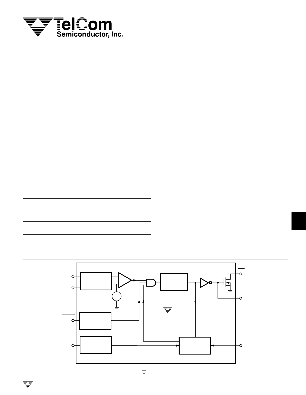
GENERAL DESCRIPTION
The TC1232 is a fully-integrated processor supervisor.
It provides three important functions to safeguard processor
sanity: precision power on/off reset control, watchdog timer
and external reset override.
On power-up, the TC1232 holds the processor in the
reset state for a minimum of 250msec after V
tolerance to ensure a stable system start-up.
Microprocessor sanity is monitored by the on-board
watchdog circuit. The microprocessor must provide a periodic low-going signal on the ST input. Should the processor
fail to supply this signal within the selected time-out period
(150msec, 600msec or 1200msec), an out-of-control processor is indicated and the TC1232 issues a processor reset
as a result.
The outputs of the TC1232 are immediately driven
active when the PB input is brought low by an external pushbutton switch or other electronic signal. When connected to
a push-button switch, the TC1232 provides contact
debounce.
The TC1232 is packaged in a space-saving 8-pin plastic
DIP or SOIC package and requires no external components.
is within
CC
2
3
4
5
FUNCTIONAL BLOCK DIAGRAM
V
CC
5%/10%
TD
TOLERANCE
SELECT
DEBOUNCE
WATCHDOG
TIMEBASE
SELECT
TOL
PB RST
TELCOM SEMICONDUCTOR, INC.
REF
RST
+
–
+
RESET
GENERATOR
TC1232
RST
6
7
ST
GND
WATCHDOG
TIMER
8
TC1232-4 11/6/96
5-19
TC1232
MICROPROCESSOR MONITOR
ABSOLUTE MAXIMUM RATINGS*
Voltage on Any Pin (With Respect to GND)
Operating Temperature Range:
TC1232C .......................................... 0°C to +70°C
TC1232E ..................................... – 40°C to + 85°C
– 0.3V to +5.8V
*Stresses beyond those listed under "Absolute Maximum Ratings" may
cause permanent damage to the device. These are stress ratings only, and
functional operation of the device at these or any other conditions beyond
those indicated in the operational sections of the specifications is not
implied. Exposure to absolute maximum rating conditions for extended
periods may affect device reliability.
Storage Temperature Range ................– 65°C to +150°C
Lead Temperature (Soldering, 10 sec) .................+300°C
DC ELECTRICAL CHARACTERISTICS: T
A
= T
MIN
to T
MAX; VCC =
+4.5V to 5.5V, unless otherwise specified.
Symbol Parameter Test Conditions Min Typ Max Unit
V
V
V
I
L
I
OH
I
OL
I
CC
V
V
CC
IH
IL
CCTP
CCTP
Supply Voltage 4.5 5.0 5.5 V
ST and PB RST 2.0 — V
+0.3 V
CC
Input High Level Note 1
ST and PB RST – 0.3 — +0.8 V
Input Low Level
Input Leakage ST, TOL – 1.0 — +1.0 µA
Output Current RST V
Current RST, RST V
= 2.4V – 1.0 –12 — mA
OH
= 0.4V 2.0 10 — mA
OL
Operating Current Note 2 — 50 200 µA
VCC 5% Trip Point (Note 3) TOL = GND 4.50 4.62 4.74 V
V
10% Trip Point (Note 3) TOL = V
CC
CC
4.25 4.37 4.49 V
CAPACITANCE (Note 4): T
= +25°C
A
Symbol Parameters Test Conditions Min Typ Max Units
C
IN
C
OUT
AC ELECTRICAL CHARACTERISTICS: T
Input Capacitance ST, TOL — — 5 pF
Output Capacitance RST, RST
A
= T
MIN
to T
MAX; VCC =
+5V to +10%, unless otherwise specified.
——7pF
Symbol Parameters Test Conditions Min Typ Max Units
t
PB
t
PBD
t
RST
t
ST
t
TD
t
F
PB RST (Note 5) Figure 3 20 — — msec
PB RST Delay Figure 3 1 4 20 msec
Reset Active Time 250 610 1000 msec
ST Pulse Width Figure 4 75 — — nsec
ST Time-out Period Figure 4
TD Pin = 0V 62.5 150 250 msec
TD Pin = Open 250 600 1000 msec
TD Pin = V
V
Fall Time (Note 4) Figure 5 10 — — µsec
CC
CC
500 1200 2000 msec
5-20
TELCOM SEMICONDUCTOR, INC.

MICROPROCESSOR MONITOR
1
TC1232
AC ELECTRICAL CHARACTERISTICS: (Cont.) T
A
= T
MIN
to T
MAX
; V
+5V to +10%, unless otherwise
CC =
specified.
Symbol Parameter Test Conditions Min Typ Max Units
t
R
t
RPD
t
RPU
NOTES: 1. PB RST is internally pulled up to VCC with an internal impedance of typically 40kΩ.
2. Measured with outputs open.
3. All voltages referenced to GND.
4. Guaranteed by design.
5. PB RST must be held low for a minimum of 20msec to guarantee a reset.
6. tR = 5µsec.
V
Rise Time (Note 4) Figure 6 0 — — µsec
CC
V
Detect to RST High Figure 7, V
CC
and RST Low
V
Detect to RST High Figure 8, V
CC
and RST Open (Note 6)
Falling — — 100 nsec
CC
Rising 250 610 1000 msec
CC
PIN CONFIGURATIONS
16-Pin SOIC Wide
1
NC
2
3
NC
TD
4
NC
5
6
TOL
NC
7
8
GND
TC1232COE
TC1232EOE
16
NC
V
15
CC
14
NC
13
ST
12
NC
RST
11
10
NC
RST
9
PB RST
TD
TOL
GND
8-Pin PDIP
V
CC
ST
RST
RST
PB RST
TD
TOL
GND
1
2
TC1232CPA
3
TC1232EPA
4
8
7
6
5
8-Pin SOIC
18
27
36
TC1232COA
TC1232EOA
45
V
CC
ST
RST
RST
PB RST
2
3
4
5
PIN DESCRIPTION
Pin No. Pin No. Pin No.
(8-Pin PDIP) (8-Pin SOIC) (16-Pin SOIC) Symbol Description
1 1 2 PB RST Push-button Reset Input. A debounced active-low input that ignores
pulses less than 1msec in duration and is guaranteed to recognize inputs
of 20msec or greater.
2 2 4 TD Time Delay Set. The watchdog time-out select input (tTD = 150msec for
TD = 0V, tTD = 600msec for TD = open, tTD = 1.2sec for TD = VCC).
3 3 6 TOL Tolerance Input. Connect to GND for 5% tolerance or to VCC for 10%
tolerance.
4 4 8 GND Ground.
5 5 9 RST Reset Output (Active High) - goes active:
1. If V
2. If PB RST is forced low
3. If ST is not strobed within the minimum time-out period
4. During power-up
6 6 11 RST Reset Output (Active Low, Open Drain) - see RST.
7 7 13 ST Strobe Input. Input for watchdog timer.
8815V
1, 3, 5, 7, 10, NC No Internal Connection.
12, 14, 16
The +5V Power-Supply Input.
CC
TELCOM SEMICONDUCTOR, INC.
falls below the selected reset voltage threshold
CC
6
7
8
5-21

TC1232
MICROPROCESSOR MONITOR
DETAILED DESCRIPTION
Power Monitor
The TC1232 detects out-of-tolerance power supply
conditions and warns a processor-based system of an
impending power failure. When VCC is detected as below the
preset level defined by TOL, the V
comparator outputs the
CC
signals RST and RST. If TOL is connected to ground, the
RST and RST signals become active as VCC falls below 4.75
volts. If TOL is connected to VCC, the RST and RST become
active as VCC falls below 4.5 volts. Because the processing
is stopped at the last possible moment of valid V
the RST
CC,
and RST are excellent control signals for a µP. The reset
outputs will remain in their active states until V
has been
CC
continuously in-tolerance for a minimum of 250msec allowing the power supply and µP to stabilize before RST is
released.
Push-button Reset Input
The debounced manual reset input (PB RST) manually
forces the reset outputs into their active states. Once
PB RST has been low for a time t
time, the reset outputs go active. The reset outputs remain
in their active states for a minimum of 250msec after PB RST
rises above VIH (Figure 3).
A mechanical push-button or active logic signal can
drive the PB RST input. The debounced input ignores input
pulses less than 1msec and is guaranteed to recognize
pulses of 20msec or greater. No external pull-up resistor is
required because the PB RST input has an internal pull-up
to VCC of approximately 100µA.
the push-button delay
PBD,
mode and set it low while in the background or interrupt
mode. If both modes do not execute correctly, the watchdog
timer issues reset pulses.
Supply Monitor Noise Sensitivity
The TC1232 is optimized for fast response to negativegoing changes in VDD. Systems with an inordinate amount
of electrical noise on VDD (such as systems using relays),
may require a 0.01µF or 0.1µF bypass capacitor to reduce
detection sensitivity. This capacitor should be installed as
close to the TC1232 as possible to keep the capacitor lead
length short.
+5V
V
CC
PB RST
Figure 1. Push-button Reset
TC1232
GND
TD
TOL
ST
RST
I/O
MICROPROCESSOR
RESET
Watchdog Timer
When the ST input is not stimulated for a preset time
period, the watchdog timer function forces RST and RST
signals to the active state. The preset time period is determined by the TD inputs to be 150msec with TD connected
to ground, 600msec with TD floating, or 1200msec with TD
connected to V
out from the set time period as soon as RST and RST are
inactive. If a high-to-low transition occurs on the ST input pin
prior to time-out, the watchdog timer is reset and begins to
time-out again. If the watchdog timer is allowed to time-out,
then the RST and RST signals are driven to the active state
for 250msec minimum (Figure 2).
The software routine that strobes ST is critical. The code
must be in a section of software that is executed frequently
enough so the time between toggles is less than the watchdog time-out period. One common technique controls the µP
I/O line from two sections of the program. The software
might set the I/O line high while operating in the foreground
5-22
typical. The watchdog timer starts timing
CC,
3 -TERMINAL
REGULATOR
+5V
10KΩ
+5V
V
CC
0.1
µF
TD
Figure 2. Watchdog Timer
RST
TC1232
ST
TOL GND
RESET
MICROPROCESSOR
I/O
TELCOM SEMICONDUCTOR, INC.

MICROPROCESSOR MONITOR
t
PB
PB RST
RST
RST
t
PBD
V
IH
V
IL
t
RST
1
TC1232
2
t
F
V
CC
+4.75V
+4.25V
3
Figure 3. Push-button Reset. The debounced PB RST input
ignores input pulses less than 1msec and is guaranteed
to recognize pulses of 20msec or greater
PUSH-BUTTON RESET
t
ST
ST
t
TD
NOTE:tTD IS THE MAXIMUM ELAPSED TIME BETWEEN ST HIGH-TO-LOW
TRANSITIONS (ST IS ACTIVATED BY FALLING EDGES ONLY) WHICH
WILL KEEP THE WATCHDOG TIMER FROM FORCING THE RESET
OUTPUTS ACTIVE FOR A TIME OF tRST. tTD IS A FUNCTION OF THE
VOLTAGE AT THE TD PIN, AS TABULATED BELOW.
t
CONDITON MIN TYP MAX
TD PIN = 0V
TD PIN = OPEN
TD PIN = V
CC
62.5msec 150msec 250msec
250msec 600msec 1000msec
500msec 1200msec 2000msec
TD
4
Figure 5. Power-Down Slew Rate
5
t
R
+4.75V
6
+4.25V
V
CC
7
Figure 4. Strobe Input
TELCOM SEMICONDUCTOR, INC.
Figure 6. Power-Up Slew Rate
8
5-23

TC1232
V
CC
4.6V (5% TRIP POINT)
4.5V(10% TRIP POINT)
RST
RST
V
OL
V
OH
t
RPU
VCC = 5V
RST
RST
+4.5V (5% TRIP POINT)
+4.25V (10% TRIP POINT)
V
OH
V
OL
t
MICROPROCESSOR MONITOR
RPD
V
SLEW RATE = 1.66mV/µsec (0.5V/300µsec)
CC
Figure 7. VCC Detect Reset Output Delay (Power-Down)
Figure 8. VCC Detect Reset Output Delay (Power-Up)
5-24
TELCOM SEMICONDUCTOR, INC.
 Loading...