TEL TR16-800-125, TR16-700-125, TR16-600-125, TR16-400-125 Datasheet

TR16 SERIES
SILICON TRIACS
l
High Current Triacs
l
16 A RMS
l
Glass Passivated Wafer
l
400 V to 800 V Off-State Voltage
l 125 A Peak Current
l
Max IGT of 50 mA (Quadrants 1 - 3)
MT1
MT2
G
TO-220 PACKAGE
(TOP VIEW)
Pin 2 is in electrical contact with the mounting base.
1
2
3
absolute maximum ratings
over operating case temperature (unless otherwise noted)
NOTES:
1. These values apply bidirectionally for any value of resistance between the gate and Main
Terminal 1
.
2. This value applies for 50-Hz full-sine-wave operation with resistive load. Above 70°C derate linearly to 110°C case temperature at
the rate of 400 mA/°C.
3. This value applies for one 50-Hz full-sine-wave when the device is operating at (or below) the rated value of peak reverse voltage
and on-state current. Surge may be repeated after the device has returned to original thermal equilibrium.
RATING SYMBOL VALUE UNIT
Repetitive peak off-state voltage (see Note 1)
TR16-400-125
TR16-600-125
TR16-700-125
TR16-800-125
V
DRM
400
600
700
800
V
Full-cycle RMS on-state current at (or below) 70°C case temperature (see Note 2) I
T(RMS)
16
A
Peak on-state surge current full-sine-wave at (or below) 25°C case temperature (see Note 3) I
TSM
12
5 A
Peak gate current I
GM
±1 A
Operating case temperature range T
C
-40 to +110 °C
Storage temperature range T
stg
-40 to +125 °C
Lead temperature 1.6 mm from case for 10 seconds T
L
230 °C
electrical characteristics at 25°C case temperature (unless otherwise noted)
PARAMETER TEST CONDITIONS MIN TYP MAX UNIT
I
DRM
Repetitive peak
off-state current
V
D
= rated V
DRM
IG = 0 TC = 110°C ±2 mA
I
GT
Gate trigger
current
V
supply
= +12 V†
V
supply
= +12 V†
V
supply
= -12 V†
V
supply
= -12 V†
R
L
= 10 W
RL = 10 W
RL = 10 W
RL = 10 W
t
p(g)
> 20 m s
t
p(g)
> 20 m s
t
p(g)
> 20 m s
t
p(g)
> 20 m s
12
-19
-16
34
50
-50
-50
mA
V
GT
Gate trigger
voltage
V
supply
= +12 V†
V
supply
= +12 V†
V
supply
= -12 V†
V
supply
= -12 V†
R
L
= 10 W
RL = 10 W
RL = 10 W
RL = 10 W
t
p(g)
> 20 m s
t
p(g)
> 20 m s
t
p(g)
> 20 m s
t
p(g)
> 20 m s
0.8
-0.8
-0.8
0.9
2
-2
-2
2
V
V
T
On-state voltage ITM = ±22.5 A IG = 50mA (see Note 4) ±1.4 ±1.7 V
I
H
Holding current
V
supply
= +12 V†
V
supply
= -12 V†
I
G
= 0
I
G
= 0
Init’ I
TM
= 100 mA
Init’ I
TM
= -100 mA
22
-1240-40
mA
† All voltages are with respect to Main Terminal 1.
NOTE 4: This parameter must be measured using pulse techniques, t
p
= £ 1 ms, duty cycle £ 2 %. Voltage-sensing contacts separate from
the current carrying contacts are located within 3.2 mm from the device body.

TR16SERIES
SILICON TRIACS
† All voltages are with respect to Main Terminal 1.
NOTE 5: The triacs are triggered by a 15-V (open-circuit amplitude) pulse supplied by a generator with the following characteristics:
R
G
= 100 W , t
p(g)
= 20 m s, tr = £ 15 ns, f = 1 kHz.
I
L
Latching current
V
supply
= +12 V†
V
supply
= -12 V†
(see Note 5)
80
-80
mA
dv/dt
Critical rate of rise of
off-state voltage
V
D
= Rated V
D
IG = 0 TC = 110°C ±400 V/µs
dv/dt
(c)
Critical rise of
commutation voltage
VD = Rated V
D
di/dt = 0.5 I
T(RMS)
/ms
T
C
= 80°C
I
T
= 1.4 I
T(RMS)
±1.2 ±9 V/µs
di/dt
Critical rate of rise of
on -state current
V
D
= Rated V
D
diG/dt = 50 mA/m s
I
GT
= 50 mA TC = 110°C ±100 A/µs
thermal characteristics
PARAMETER MIN TYP MAX UNIT
R
q JC
Junction to case thermal resistance 1.9 °C/W
R
q JA
Junction to free air thermal resistance 62.5 °C/W
electrical characteristics at 25°C case temperature (unless otherwise noted) (continued)
PARAMETER TEST CONDITIONS
MI
N TYP MAX UNIT
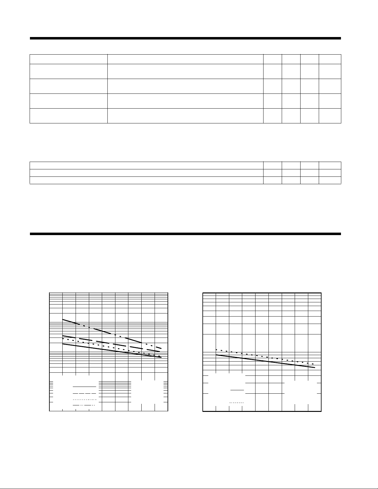
TYPICAL CHARACTERISTICS
Figure 1. Figure 2.
GATE TRIGGER CURRENT
TC - Case Temperature - °C
-60 -40 -20 0 20 40 60 80 100 120
I
GT
- Gate Trigger Current - mA
0·1
1
10
100
1000
CASE TEMPERATURE
vs
V
supply IGTM
+ +
+ -
- -
- +
VAA = ± 12 V
RL = 10 W
W
t
p(g)
= 20 µs
GATE TRIGGER VOLTAGE
TC - Case Temperature - °C
-60 -40 -20 0 20 40 60 80 100 120
V
GT
- Gate Trigger Voltage - V
0·1
1
10
CASE TEMPERATURE
vs
VAA = ± 12 V
RL = 10 W
W
t
p(g)
= 20 µs
V
supply IGTM
+ +
+ -
- -
- +
}
 Loading...