

Page 1

Instruction Manual
TMSSN1 478 Pin Socket Hardware Support
071-0896-01
Warning
The servicing instructions are for use by qualified
personnel only. To avoid personal injury, do not
perform any servicing unless you are qualified to
do so. Refer to all safety summaries prior to
performing service.
www.tektronix.com
Page 2

Copyright © Tektronix, Inc. All rights reserved.
Tektronix products are covered by U.S. and foreign patents, issued and pending. Information in this publication supercedes
that in all previously published material. Specifications and price change privileges reserved.
Tektronix, Inc., P.O. Box 500, Beaverton, OR 97077
TEKTRONIX and TEK are registered tradem arks of Tektronix, Inc.
Page 3

HARDWARE WARRANTY
Tektronix warrants that the products that it m anufactures and sells will be free from defects in materials and
workmanship for a period of one (1) year from the date of shipment. If a product proves defective during this
warranty period, Tektronix, at its option, either will repair the defective product without charge for parts and labor,
or will provide a replacement in exchange for the defective product.
In order to obtain service under this warranty, Customer must notify Tektronix of the defect before the expiration
of the warranty period and make suitable arrangements for the performance of service. Customer shall be
responsible for packaging and shipping the defective product to the service center designated by Tektronix, with
shipping charges prepaid. Tektronix shall pay for the return of the product to Customer if the shipment is to a
location within the country in which the Tektronix service center is located. Customer shall be responsible for
paying all shipping charges, duties, taxes, and any other charges for products returned to any other locations.
This warranty shall not apply to any defect, failure or damage caused by improper use or improper or inadequate
maintenance and care. Tektronix shall not be obligated to furnish service under this warranty a) to repair damage
resulting from attempts by personnel other than Tektronix representatives to install, repair or service the product;
b) to repair damage resulting from improper use or connection to incompatible equipment; c) to repair any
damage or malfunction caused by the use of non-Tektronix supplies; or d) to service a product that has been
modified or integrated with other products when the effect of such modific ation or integration increases the time
or difficulty of servicing the product.
THIS W ARRANTY IS GIVEN BY TEKTRONIX IN LIEU OF ANY OTHER W ARRANTIES, EXPRESS
OR IMPLIED. TEKTRONIX AND ITS VENDORS DISCLAIM ANY IMPLIED WARRANTIES OF
MERCHANTABILITY OR FITNESS FOR A PARTICULAR PURPOSE. TEKTRONIX’
RESPONSIBILITY TO REPAIR OR REPLACE DEFECTIVE PRODUCTS IS THE SOLE AND
EXCLUSIVE REMEDY PROVIDED TO THE CUSTOMER FOR BREACH OF THIS WARRANTY.
TEKTRONIX AND ITS VENDORS WILL NOT BE LIABLE FOR ANY INDIRECT, SPECIAL,
INCIDENTAL, OR CONSEQUENTIAL DAMAGES IRRESPECTIVE OF WHETHER TEKTRONIX OR
THE VENDOR HAS ADVANCE NOTICE OF THE POSSIBILITY OF SUCH DAMAGES.
Page 4

Page 5

Table of Contents
Getting Started
General Safety Summary vii..........................................
Service Safety Summary ix...........................................
Preface xi...................................................
Manual Conventions xi..............................................
Contacting Tektronix xii..............................................
Getting Started 1--1............................................
Support Package Description 1--1.......................................
Support Software Compatibility 1--1.....................................
Logic Analyzer Configuration 1--1......................................
Probe Adapter Review 1--2............................................
Labeling P6434 Probes 1--3............................................
Standard Accessories 1--4.............................................
Options 1--4........................................................
Configuring the Probe Adapter 1--4......................................
PLL OFF Jumper 1--5.............................................
Frequency Select Jumper 1--5.......................................
Connecting the Logic Analyzer to a Target System 1--5......................
Removing the Probe Head from the Target System 1--13...................
Alternate Connections 1--17.............................................
Software Support 1--17................................................
Verifying Probe Operation 1--18........................................
Storage 1--19........................................................
Care and Maintenance 1--20.............................................
Shipping the Probe Adapter 1--21........................................
Specifications
Specifications 2--1............................................
Circuit Description 2--1...............................................
Probe Adapter Loading Diagrams 2--3....................................
Specification Tables 2--5..............................................
Reference
Reference: Channel Assignment Tables 3--1.......................
Channel Assignments 3--1.............................................
Maintenance
Maintenance 4--1..............................................
Fuses 4--1..........................................................
Removal and Installation Procedures 4--3.........................
Removing the Cables 4--3.............................................
Replacing the Cables 4--8..............................................
Shipping the Probe Head and Cables 4--10.................................
TMSSN1 478 Pin Socket Hardware Support
i
Page 6

Table of Contents
Replaceable Parts List
Index
Reinstalling the Cables 4--12............................................
Removing and Instaling a Fan 4--16......................................
Replaceable Parts List 5--1......................................
Parts Ordering Information 5--1.........................................
Using the Replaceable Parts List 5--2.....................................
ii
TMSSN1 478 Pin Socket Hardware Support
Page 7

List of Figures
Table of Contents
Figure 1--1: Configuration of the master, slave, and
slave 2 modules 1--2........................................
Figure 1--2: Jumper locations on the preprocessor unit 1--4...........
Figure 1--3: Configuration for master and slave modules 1--6.........
Figure 1--4: Removing the heat sink retention mechanism
from the target system 1--7..................................
Figure 1--5: Install the base-bracket feet 1--8.......................
Figure 1--6: Connect the probe head to the target system 1--9.........
Figure 1--7: Connecting the microprocessor, probe head,
and target system 1--10.......................................
Figure 1--8: Placing the heat sink on the probe head 1--11.............
Figure 1--9: Attaching the spring clips to the heat sink 1--12...........
Figure 1--10: Connecting probes 1--14..............................
Figure 1--11: Configuration of the master, slave, and
slave 2 modules 1--14........................................
Figure 1--12: Operating the probe latches 1--15......................
Figure 2--1: Electrical load model for typical signals 2--3.............
Figure 2--2: Pin header electrical load model for typical signals 2--4...
Figure 2--3: ZIF electrical load model for typical signals 2--4.........
Figure 2--4: Mated Samtec model 2--4.............................
Figure 2--5: BCLK Receiver 2--4.................................
Figure 2--6: Dimensions of the 478 Pin Socket probe head 2--8........
Figure 2--7: Dimensions of the preprocessor unit 2--9................
Figure 3--1: Configuration of the master, slave, and slave 2,
modules 3--1...............................................
Figure 4--1: Probe head and preprocessor unit 4--4..................
Figure 4--2: Remove AC power cord 4--4..........................
Figure 4--3: Remove the attaching screws 4--5......................
Figure 4--4: Remove the bottom cover 4--5.........................
Figure 4--5: Remove the cables from the logic board 4--6.............
Figure 4--6: Remove the cables from the probe head 4--7.............
Figure 4--7: Probe-head cable end 4--8............................
Figure 4--8: Preprocessor cable end 4--9...........................
Figure 4--9: Check corners 4--10..................................
Figure 4--10: Power switch location 4--12...........................
Figure 4--11: Dress the cables through the side opening 4--13..........
TMSSN1 478 Pin Socket Hardware Support
iii
Page 8

Table of Contents
Figure 4--12: Attach the cables to the logic board cover plate 4--13......
Figure 4--13: Attach the bottom cover 4--14.........................
Figure 4--14: Place the heat sink on the probe head 4--15..............
Figure 4--15: Power switch and AC power cord locations 4--16.........
Figure 4--16: Remove the attaching screws 4--17.....................
Figure 4--17: Remove the bottom cover 4--17........................
Figure 4--18: Remove the pin connectors 4--18.......................
Figure 4--19: Back of the preprocessor unit 4--19....................
Figure 4--20: Location of fan connector 4--20........................
Figure 5--1: 478 Pin Socket probe adapter exploded view 5--6.........
Figure 5--2: Preprocessor unit exploded view 5--8...................
iv
TMSSN1 478 Pin Socket Hardware Support
Page 9

List of Tables
Table of Contents
Table 1--1: Default Jumper Positions 1--5.........................
Table 1--2: Frequency Select Jumpers 1--5........................
Table 2--1: Electrical specifications for the target system 2--5........
Table 2--2: Electrical specifications for the AC input to the
preprocessor unit 2--5......................................
Table 2--3: BCLK timing and electrical specifications 2--6..........
Table 2--4: Environmental specifications 2--6......................
Table 2--5: Certifications and compliances 2--7....................
Table 3--1: Clock channel assignments 3--2........................
Table 3--2: Qualifier channel assignments 3--2.....................
Table 3--3: Master Module 32-channel Address assignments 3--3......
Table 3--4: Master Module 32-channel Data assignments 3--4.........
Table 3--5: Master Module 32-channel Control assignments 3--5......
Table 3--6: Master Module 32-channel Extend assignments 3--7.......
Table 3--7: Slave Module 32-channel Address assignments 3--8.......
Table 3--8: Slave Module 32-channel Data assignments 3--9..........
Table 3--9: Slave Module 32-channel Control assignments 3--10........
Table 3--10: Slave Module 32-channel Extend assignments 3--12.......
Table 3--11: Slave 2 Module 32-channel Address assignments 3--13.....
Table 3--12: Slave 2 Module 32-channel Data assignments 3--14........
Table 3--13: Slave 2 Module 32-channel Control assignments 3--15.....
Table 3--14: Slave 2 Module 32-channel Extended assignments 3--17....
Table 3--15: Signals not available on the probe adapter 3--18..........
TMSSN1 478 Pin Socket Hardware Support
v
Page 10

Table of Contents
vi
TMSSN1 478 Pin Socket Hardware Support
Page 11

General Safety Summary
Review the following safety precautions to avoid injury and prevent damage to
this product or any products connected to it. To avoid potential hazards, use this
product only as specified.
Only qualified personnel should perform service procedures.
While using this product, you may need to access other parts of the system. Read
the General Safety Summary in other system manuals for warnings and cautions
related to operating the system.
ToAvoidFireor
Personal Injury
Use Proper Power Cord. Use only the power cord specified for this product and
certified for the country of use.
Connect and Disconnect Properly. Do not connect or disconnect probes or test
leads while they are connected to a voltage source.
Ground the Product. This product is grounded through the grounding conductor
of the power cord. To avoid electric shock, the grounding conductor must be
connected to earth ground. Before making connections to the input or output
terminals of the product, ensure that the product is properly grounded.
Observe All Terminal Ratings. To avoid fire or shock hazard, observe all ratings
and markings on the product. Consult the product manual for further ratings
information before making connections to the product.
Connect the ground lead of the probe to earth ground only.
Do Not Operate Without Covers. Do not operate this product with covers or panels
removed.
Use Proper Fuse. Use only the fuse type and rating specified for this product.
Avoid Exposed Circuitry. Do not touch exposed connections and components
when power is present.
Do Not Operate With Suspected Failures. If you suspect there is damage to this
product, have it inspected by qualified service personnel.
Do Not Operate in Wet/Damp Conditions.
Do Not Operate in an Explosive Atmosphere.
Keep Product Surfaces Clean and Dry.
Provide Proper Ventilation. Refer to the manual’s installation instructions for
details on installing the product so it has proper ventilation.
TMSSN1 478 Pin Socket Hardware Support
vii
Page 12

General Safety Summary
Symbols and Terms
Terms in this Manual. These terms may appear in this manual:
WARNING. Warning statements identify conditions or practices that could result
in injury or loss of life.
CAUTION. Caution statements identify conditions or practices that could result in
damage to this product or other property.
Terms on the Product. These terms may appear on the product:
DANGER indicates an injury hazard immediately accessible as you read the
marking.
WARNING indicates an injury hazard not immediately accessible as you read the
marking.
CAUTION indicates a hazard to property including the product.
Symbols on the Product. The following symbols may appear on the product:
CAUTION
Refer to Manual
WARNING
High Voltage
Protective Ground
(Earth) Terminal
viii
TMSSN1 478 Pin Socket Hardware Support
Page 13

Service Safety Summary
Only qualified personnel should perform service procedures. Read this Service
Safety Summary and the General Safety Summary before performing any service
procedures.
Do Not Service Alone. Do not perform internal service or adjustments of this
product unless another person capable of rendering first aid and resuscitation is
present.
Disconnect Power. To avoid electric shock, switch off the instrument power, then
disconnect the power cord from the mains power.
Use Care When Servicing With Power On. Dangerous voltages or currents may
exist in this product. Disconnect power, remove battery (if applicable), and
disconnect test leads before removing protective panels, soldering, or replacing
components.
To avoid electric shock, do not touch exposed connections.
TMSSN1 478 Pin Socket Hardware Support
ix
Page 14

Service Safety Summary
x
TMSSN1 478 Pin Socket Hardware Support
Page 15

Preface
Manual Conventions
This instruction manual contains specific information about the
TMSSN1 478 Pin Socket microprocessor support package and is part of a set of
information on how to operate this product on compatible Tektronix logic
analyzers.
If you are familiar with operating microprocessor support packages on the logic
analyzer, all you need is this instruction manual to set up and run the support
package.
If you are not familiar with operating microprocessor support packages, you need
to supplement this instruction manual with information on basic operations from
the Tektronix logic analyzer online help to set up and run the support package.
This manual uses the following conventions:
H A pound sign (#) following a signal name indicates an active low signal.
H The phrase “information on basic operations” refers to basic information in
your logic analyzer online help.
H The terms “Master,” “Slave,” and “Slave2” refer to modules that are located
in numbered slots (see Figure 1--1 on page 1--2).
TMSSN1 478 Pin Socket Hardware Support
xi
Page 16

Preface
Contacting Tektronix
Phone 1-800-833-9200*
Address Tektronix, Inc.
Department or name (if known)
14200 SW Karl Braun Drive
P.O. Box 500
Beaverton, OR 97077
USA
Web site www.tektronix.com
Sales support 1-800-833-9200, select option 1*
Service support 1-800-833-9200, select option 2*
Technical support Email: techsupport@tektronix.com
1-800-833-9200, select option 3*
6:00 a.m. -- 5:00 p.m. Pacific time
* This phone number is toll free in North America. After office hours, please leave a
voice mail message.
Outside North America, contact a Tektronix sales office or distributor; see the
Tektronix web site for a list of offices.
xii
TMSSN1 478 Pin Socket Hardware Support
Page 17

Getting Started
Page 18

Page 19

Getting Started
This section contains information on the TMSSN1 478 Pin Socket hardware
support package and information on connecting the logic analyzer to the target
system.
Support Package Description
The probe adapter is nonintrusive hardware that allows the logic analyzer to
acquire data from a microprocessor in the operating environment with little effect
on the target system.
The probe adapter is an interposer design. The probe adapter connects to the
target system, and then the microprocessor connects to the probe adapter. Signals
from the microprocessor-based system flow through the probe adapter into the
P6434 probes and through the probe cables to the logic analyzer.
Support Software Compatibility
The probe adapter is compatible with the TMS116 IA32G7 software support
package that provides timing analysis capabilities, synchronous transactions, and
instruction decoding.
Logic Analyzer Configuration
To use the TMSSN1 478 Pin Socket hardware support package you need a
Tektronix logic analyzer equipped with a minimum of three, 136-channel,
200 MHz merged modules for the IA32G7 support and a minimum of two,
136-channel, 200 MHz merged modules for the IA32G7_T. Both software
support packages may be used in parallel in one logic analyzer mainframe.
However, this is not a requirement.
The modules must be configured and merged as shown in Figure 1--1. The
memory depth is chosen based on the shallowest memory depth of the three
modules. The master module must have the deeper memory depth.
The TMSSN1 478 Pin Socket hardware and software package is compatible only
with version 3.2 or later Tektronix logic analyzer application software.
The probe adapter requires a minimum of twelve P6434 Mass Termination
Probes.
TMSSN1 478 Pin Socket Hardware Support
1--1
Page 20

Getting Started
Slave 2 Master Slave
Figure 1--1: Configuration of the master, slave, and slave 2 modules
Probe Adapter Review
The term “Master module” refers to the middle module of a 3-way merge. The
term “Slave module” refers to the module in the higher numbered slot than the
master module. The term “Slave 2” module refers to the module in the lower
numbered slot than the master module.
CAUTION. To keep the microprocessor from overheating, a forced air cooling
solution must be used.
Review the information on basic operations of microprocessor support packages
that is included with each logic analyzer product. Each logic analyzer includes
information that describes how to perform tasks common to support packages on
that platform. This information can be in the form of the logic analyzer online
help, an installation manual, or a user manual.
Also, review electrical, environmental, and mechanical specifications in
Specifications on page 2--1 as they pertain to the target system, as well as the
following TMSSN1 478 Pin Socket probe adapter information.
1--2
TMSSN1 478 Pin Socket Hardware Support
Page 21

Getting Started
System Clock Rate
Acquisition before Reset
BCLK
Data Bus
Address Bus
Disabling the Cache
The probe adapter can acquire data from the 478 Pin Socket microprocessor
operating at BCLK speeds of up to 133 MHz.
Contact the Tektronix sales representative for current information on the fastest
devices supported.
The data acquired by the logic analyzer will be inaccurate, if this data is acquired
just before a power on Reset signal is observed by the target system.
Refer to the BCLK specifications and restrictions listed on page 2--6, in the
Specifications section.
The probe adapter supports only a quad-pumped data bus.
The probe adapter supports only a double-pumped address bus.
The cache bus is not monitored, therefore, the cache must be disabled. Disabling
the cache makes all instruction prefetches visible on the bus so they can be
acquired, displayed, and correctly disassembled.
Data Skew viewed at the
Timing Mictors
Labeling P6434 Probes
On the timing mictors, all data is skewed from the clock by
approximately --900 ps. This means that when you use an oscilloscope, you will
see the data changing approximately 900 ps earlier than you should as compared
to the FSB clock. However, there is one exception; the RESET# signal is
approximately 500 ps earlier than the FSB clock. The data skew seen when using
the oscilloscope does not affect the state acquisitions in any way.
The TMSSN1 478 Pin Socket hardware support package relies on the standard
channel mapping and labeling scheme for P6434 probes. Apply labels using the
standard method described in the P6434 Mass Termination Probe Instructions.
TMSSN1 478 Pin Socket Hardware Support
1--3
Page 22

Getting Started
Standard Accessories
The TMSSN1 478 Pin Socket Support package is shipped with the following
standard accessories:
H Technical manual (1)
H Heat sink and fan assembly (1)
H AC power cord (1)
Options
See the Replaceable Parts List on page 5--4 for more detailed information.
Configuring the Probe Adapter
The probe adapter is configured by the jumpers shown in Tables 1--1 and 1--2.
Figure 1--2 shows the location of all jumpers.
1--4
Frequency select
J10, J11, J12
PLL OFF J9
Figure 1--2: Jumper locations on the preprocessor unit
TMSSN1 478 Pin Socket Hardware Support
Page 23

Getting Started
PLL OFF Jumper
Frequency
Select Jumper
Default jumper information is listed in Table 1--1. For operation frequencies
below 20 MHz, place the jumper in the Pin 2--3 position. Placing the jumper in
the Pin 2--3 position by passes the PLL.
Table 1--1: Default Jumper Positions
Default pin posi-
Jumper name
PLL OFF 1--2 J9
S1 1--2 J10
S2 1--2 J11
S3 1--2 J12
tion
Jumper
Designation
For the Frequency Select Jumper settings see Table 1--2 for the appropriate
operating frequency.
Table 1--2: Frequency Select Jumpers
Frequency S1 (J10) S2 (J11) S3 (J12)
140 -- 230 Mhz 1--2 2--3 2--3
70 -- 140 Mhz 1--2 1--2 1--2
30 -- 70 Mhz 1--2 1--2 2--3
20 -- 30 Mhz 2--3 1--2 2--3
Below 20 MHz PLL_OFF jumper (see Table 1--1)
Connecting the Logic Analyzer to a Target System
CAUTION. To prevent static damage to the microprocessor, the probe adapter, the
probes, and the module, you must handle components only in a static-free
environment.
Always wear a grounding wrist strap, heel strap, or similar device while
handling the microprocessor and probe adapter.
Before you connect the probe adapter to the target system, connect twelve P6434
probes to the Master, Slave, and Slave 2 modules. For reference, Figure 1--3
shows the configuration for the Master, Slave and Slave 2 modules.
TMSSN1 478 Pin Socket Hardware Support
1--5
Page 24

Getting Started
Slave 2 Master Slave
Figure 1--3: Configuration for master and slave modules
Tools Required
The target system must allow clearance for the probe adapter. Refer to the
dimensions on page 2--9 for the required clearances.
The following are the required tools:
H Flat-bladed screwdriver (0.1 inch tip width) to remove the heat sink retention
module
H POZIDRIV screwdriver (PZ1) to attach the probe head to the target system
CAUTION. To prevent static damage to the microprocessor, the probe adapter, the
probes, and the module, handle components only in a static-free environment.
Always wear a grounding wrist strap, heel strap, or similar device while
handling the microprocessor and probe adapter.
Read the following general instructions before removing parts.
To connect the logic analyzer to the target system, follow these steps:
1. Power off the target system. It is not necessary to power off the logic
analyzer.
1--6
2. To discharge any static electricity, touch the ground connector located on the
logic analyzer.
3. On the target system, remove the heat sink from the microprocessor and set
the heat sink aside.
TMSSN1 478 Pin Socket Hardware Support
Page 25

Getting Started
4. Deactivate the ZIF socket on the target system.
5. Remove the microprocessor from the target system following the removal
procedure from the microprocessor vendor.
6. Remove the heat sink retention mechanism from the target system by
removing the center post from each rivet (see Figure 1--4).
Center post
heat sink
retention
mechanism
Target
system
Figure 1--4: Removing the heat sink retention mechanism from the target system
TMSSN1 478 Pin Socket Hardware Support
1--7
Page 26

Getting Started
The 478 Pin Socket probe head comes assembled, except for the alignment feet.
It is recommend that you use the alignment feet to guide the probe head into position
when connecting to the target system.
Steps 1 and 2 describe how to attach the alignment feet to the target system.
1. Slide the center pin down into the alignment foot (see Figure 1--5).
Target system rest
on this surface
Alignment foot
Heat sink retention
holes
Target system
Slide the pin all the
way down into the
foot
Target system
Push the plastic
foot down into
the board
The pin catches
underneath the board
1--8
Figure 1--5: Install the base-bracket feet
2. Install the alignment foot into the heat sink retention holes on the target
system (see Figure 1--5). Repeat steps 1 and 2 for each alignment foot.
CAUTION. To prevent damage to the probe head and pins, you must always
handle the probe head carefully and use care to properly align the probe head
pins to the ZIF socket on the target system. Also, reinstall the pin protector to the
bottom of the probe head when the probe head is not in use.
3. Deactivate the ZIF socket on the target system (see Figure 1--6).
4. Remove the pin protector board from the bottom of the probe head.
TMSSN1 478 Pin Socket Hardware Support
Page 27

Getting Started
5. Remove the tape that covers the socket holes on the probe head.
6. Connect the probe pin head to the socket on the target system. Use the
alignment feet to guide the probe head into position. You must visually verify
proper pin alignment between the probe-head pins and the socket on the
target system.
Screws (4)
Probe
head
Lift the handle up
to deactivate the
ZIF socket
system
Figure 1--6: Connect the probe head to the target system
7. Activate the ZIF socket on the target system.
TMSSN1 478 Pin Socket Hardware Support
Target
1--9
Page 28
Getting Started
8. With a POZIDRIVR screwdriver (PZ1), gently attach the screws to the
probe head using 2 in-lbs (0.2 Newton meters) of torque to secure the probe
head to the target system (see Figure 1--6 on page 1--9).
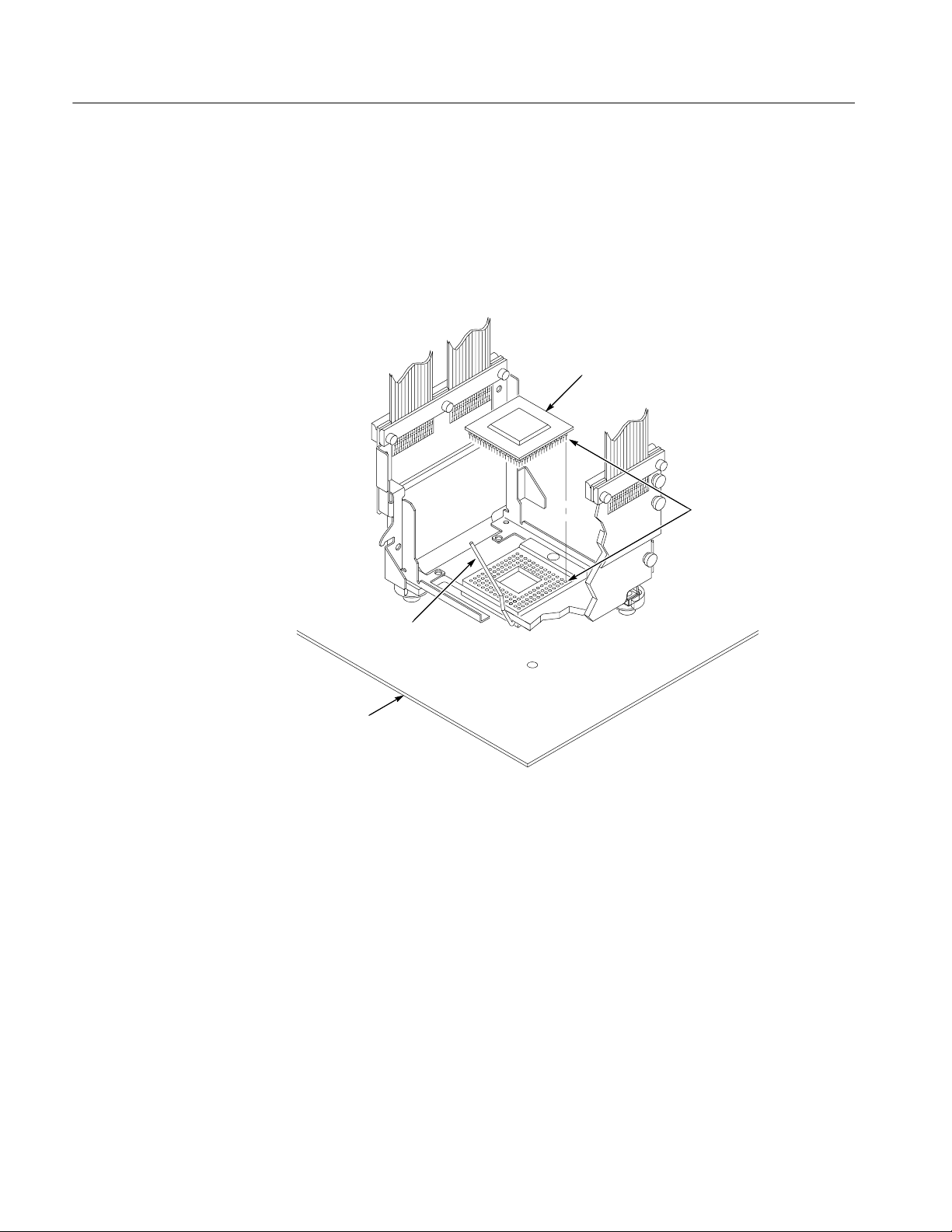
9. Connect the microprocessor to the ZIF socket in the probe head. Align the
microprocessor A1 pin indicator with the socket A1 pin indicator, and set the
microprocessor into place as shown in Figure 1--7.
Microprocessor
Pin A1
Lock handle
down
Target
system
Figure 1--7: Connecting the microprocessor, probe head, and target system
10. Activate the ZIF socket on the probe head.
1--10
TMSSN1 478 Pin Socket Hardware Support
Page 29

Getting Started
11. Place the air cooled heat sink and fan on top of the microprocessor as shown
in Figure 1--8. You may need to use thermal grease for better contact between
the heat sink and the microprocessor. For thermal requirements, refer to the
microprocessor vendor information.
CAUTION. To prevent damage to the microprocessor, you must use the cooling fan
that is provided with the heat sink whenever you operate the TMSSN1 478 Pin
Socket probe adapter.
Heat sink
and fan
Target
system
Figure 1--8: Placing the heat sink on the probe head
TMSSN1 478 Pin Socket Hardware Support
1--11
Page 30

Getting Started
12. Attach the spring clips to both sides of the heat sink (see Figure 1--9).
CAUTION. To prevent damage to the microprocessor, you must not rock the probe
head when attaching the spring clips. But you can press the top of the heat sink
assembly to the microprocessor while installing the spring clips.
Spring clips (2)
Target system
Figure 1--9: Attaching the spring clips to the heat sink
13. Connect the fan connector to the target system.
1--12
TMSSN1 478 Pin Socket Hardware Support
Page 31

Getting Started
Removing the Probe Head
from the Target System
To remove the probe head from the target system, follow these steps:
1. Power off the target system, and then the preprocessor unit. It is not
necessary to power off the logic analyzer.
2. Disconnect the fan connector from the target system.
3. Remove both spring clips from the heat sink (see Figure 1--9 on page 1--12).
4. Remove the heat sink and fan assembly from the microprocessor (see
Figure 1--8 on page 1--11).
5. Deactivate the ZIF socket on the target system (see Figure 1--7 on page
1--10).
6. Remove the microprocessor from the probe head and place in protective
packaging.
7. Remove the screws (see Figure 1--6 on page 1--9) that connect the probe
head to the target system using a POZIDRIV screwdriver (PZ1).
8. Disconnect the probe head from the 478 Pin Socket socket on the target
system.
9. Install the pin-protector cover to the bottom of the probe head.
10. Disconnect the preprocessor unit from the Tektronix logic analyzer.
11. Store the probe head as describe in Storage on page 1--19.
TMSSN1 478 Pin Socket Hardware Support
1--13
Page 32

Getting Started
Connect the P6434 Probes
to the Preprocessor Unit
Mictor connectors (P6434) may be configured for timing or disassembly support
functions. For reference, Figure 1--10 shows the Mictor connectors attached to
the preprocessor unit.
Figure 1--10: Connecting probes
Figure 1--11 shows the configuration for the Master, Slave, and Slave 2 modules.
Slave 2 Master Slave
Figure 1--11: Configuration of the master, slave, and slave 2 modules
1--14
TMSSN1 478 Pin Socket Hardware Support
Page 33
Getting Started
Disassembly. Following is the minimum configuration for disassembly support.
1. Match the A, D, C, and E probes from the Slave2 module with the corre-
sponding S2_A_DIS, S2_D_DIS, S2_C_DIS, and S2_E_DIS probe
connector labels on the preprocessor unit. Align the Pin 1 indicator on the
probe label with the Pin 1 indicator of the connector on the preprocessor unit.
CAUTION. To prevent damage to the probe and preprocessor unit, you must
always position the probe perpendicular to the mating connector with Pin 1s
aligned and gently connect the probe. Incorrect handling of the P6434 probe
while connecting to or disconnecting from the preprocessor can damage the
probe or the mating connector on the preprocessor unit.
2. Position the probe tip perpendicular to the mating connector and gently
connect the probe (see Figure 1--12).
3. When connected, push down on the latch releases on the probe to set the
latch.
Push down to latch after
probe is connected
Pin 1
Pin 1
Push down to latch after
probe is connected
Figure 1--12: Operating the probe latches
4. Match the A, D, C, and E probes from the Master module with the corre-
sponding M_A_DIS, M_D_DIS, M_C_DIS, and M_E_DIS probe connectors
labels on the preprocessor unit. Align the Pin 1 indicator on the probe label
with the Pin 1 indicator of the connector on the preprocessor unit.
5. Repeat steps 2 and 3 to connect additional probes.
TMSSN1 478 Pin Socket Hardware Support
1--15
Page 34

Getting Started
6. Match the A, D, C, and E probes from the Slave module with the correspond-
ing S_A_DIS, S_D_DIS, S_C_DIS and S_E_DIS probe connector labels on
the preprocessor unit. Align the Pin 1 indicator on the probe label with Pin 1
of the connector on the preprocessor unit (see Figure 1--12).
7. Repeat steps 2 and 3 to connect additional probes.
Timing. Following is the minimum configuration for timing support.
1. Match the A, D, C, and E probes from the Master module with the corre-
sponding M_A_TMG, M_D_TMG, M_C_TMG, and M_E_TMG probe
connectors labels on the preprocessor unit. Align the pin 1 indicator on the
probe label with the Pin 1 indicator of the connector on the preprocessor unit.
CAUTION. To prevent damage to the probe and preprocessor unit, always position
the probe perpendicular to the mating connector and gently connect the probe.
Incorrect handling of the P6434 probe while connecting to or disconnecting from
the probe adapter can damage the probe or the mating connector on the
preprocessor unit.
Applying Power
2. Position the probe tip perpendicular to the mating connector, and gently
connect the probe (see Figure 1--12).
3. When connected, push down the latch releases on the probe to set the latch.
4. Match the A, D, C, and E probes from the Slave module with the correspond-
ing S_A_TMG, S_D_TMG, S_C_TMG and S_E_TMG probe connector
labels on the preprocessor unit. Align the Pin 1 indicator on the probe label
with Pin 1 of the connector on the preprocessor unit (see Figure 1--12).
5. Repeat steps 2 and 3 to connect additional probes.
6. Apply forced air cooling across the microprocessor to keep the microproces-
sor from overheating, if using an air-cooled heat sink.
To apply power to the probe adapter and target system, follow these steps:
1. Make sure the power switch on the preprocessor unit is in the off position
(zero (0) is visible on the power switch). See Figure 4--2 on page 4--4 for the
location of the power switch.
WARNING. To prevent personal injury or damage to the preprocessor unit, there
are no operator serviceable parts inside the cover of the preprocessor unit. Refer
servicing of internal parts in the preprocessor unit to Tektronix authorized
personnel only.
1--16
TMSSN1 478 Pin Socket Hardware Support
Page 35

Getting Started
2. Plug the AC power cord into the IEC connector on the back of the preproces-
sor unit.
3. Plug the AC power cord into an electrical outlet that you know is working
properly.
4. Power on the preprocessor unit. A green LED lights on the front of the
preprocessor unit, indicating the probe is active. If the LED does not light,
see page 1--18 to verify the probe operation.
5. Power on the target system.
Removing Power
Alternate Connections
Software Support
To remove power from the target system and the probe adapter, follow these
steps:
1. Power off the target system.
2. Power off the probe adapter at the back of the preprocessor unit.
Timing Connections. Timing connections are available. For the correct probe
connections, see page 1--16 to connect from the logic analyzer to the preprocessor. Use the IA32G7_T software configuration for the timing function.
Disassembly. Disassembly and Timing connections are available. For the correct
probe connections, see page 1--14 to connect from the logic analyzer to the
preprocessor unit. Use the IA32G7 software configuration for the disassembly
function.
Timing Connections. For the correct probe connections, see page 1--16 to connect
from the logic analyzer to the preprocessor unit. Use the IA32G7_T software
configuration for the timing function.
TMSSN1 478 Pin Socket Hardware Support
1--17
Page 36
Getting Started
Verifying Probe Operation
If you have trouble using the probe adapter to acquire data from the target
system, you can use the following check list to ensure that the probe adapter and
probe-head cables are working correctly.
WARNING. To prevent personal injury or damage to the preprocessor unit, cables
and fans need to be replaced by qualified service personnel only.
There are no operator serviceable parts inside the cover of the preprocessor unit.
Refer servicing of internal parts in the preprocessor unit to Tektronix authorized
personnel only.
1. Check that power is supplied to the preprocessor unit by observing the
lighted green LED on the front of the case. If the LED is not lighted:
H Check that the power switch on the back of the preprocessor unit is
powered on. If powered off, a 0 (zero) is visible on the switch.
H Check that the AC power cord is plugged into an electrical outlet that
you know is working properly.
H If the LED is still not lighted, unplug the unit from the electrical outlet
and call a Tektronix Service representative. Only authorized service
personnel can open the preprocessor unit to check the probe head cable
connections.
2. Check that the phase-locked loop of the probe adapter is set to the proper
frequency range. Use the following procedure to determine the clock
frequency of the target system:
a. On top of the preprocessor unit, set the PLL-OFF jumper to the 2--3 pin
position (phase-locked loop is off).
b. Acquire the BCLK using MagniVu.
c. Calculate the frequency based on the rising or falling BCLK edges.
d. On top of the preprocessor unit, set the frequency select jumpers (S3, S2,
and S1) to the appropriate frequency range (see page 1--4).
e. On top of the preprocessor unit, set the PLL-OFF jumper to 1--2 position
(phase-lock loop on) if the frequency of the target system is within the
PLL range.
1--18
3. Check that the ASICs are being programmed by looking through the Mictor
connector openings on top of the preprocessor unit. If the ASICs are being
programmed, the six green “program-good” LEDs are visible and lighted. If
TMSSN1 478 Pin Socket Hardware Support
Page 37

Getting Started
none of the LEDs are lighted, power off and on the probe adapter using the
power switch.
4. Check that signals are passing through the Mictor connectors by using the
following procedure:
a. Go to the Setup menu and select “show activity”.
b. Visually verify from the display that signals are transitioning on each
Mictor connector.
c. If the signals are not transitioning, you can wiggle the Mictor connector
on top of the preprocessor unit slightly to check that it is fully seated.
d. If the signals are still not transitioning, disconnect the Mictor probe from
that socket in the preprocessor unit and connect that Mictor probe into a
socket that indicates signal transitioning.
e. If the channels never transition:
H Check the Mictor probe for bent contacts.
Storage
Short-Term Storage
Long-Term Storage
H Check the probe adapter for bent Mictor contacts.
If performing the preceding bullets did not correct the problem, replace
the existing Mictor probe with a new Mictor probe.
The storage instructions describe short- and long-term storage of the probe head,
cables, and preprocessor unit.
For short-term storage follow these steps:
1. Power off the probe adapter. You can leave the logic analyzer powdered on.
2. Disconnect the probe head from the target system (See page 1--13).
3. Wrap pink (antistatic) bubble wrap around the probe head, and store the
probe head with the preprocessor unit.
For long-term storage use the existing cardboard carton and packaging, and
follow these steps:
1. Power off the probe adapter. You can leave the logic analyzer powdered on.
2. Disconnect the preprocessor unit from the logic analyzer by removing the
P6434 probes from the top of the preprocessor unit.
TMSSN1 478 Pin Socket Hardware Support
1--19
Page 38
Getting Started
3. Unplug the AC power cord from the IEC connector on the back of the
preprocessor unit.
4. Disconnect the probe head from the target system (see page 1--13).
5. Place the foam end caps on both sides of the preprocessor unit. The
depression on the foam end caps are in the up position.
6. Place the preprocessor unit inside the cardboard carton.
7. Place the pink-foam panel on top of the end caps.
8. Place the probe head in the center cutout of the pink-foam panel.
CAUTION. To prevent damage to the sensitive probe head cables, dress the cables
to not pinch or contact any sharp objects. When you fold the cables use a
minimum of 0.25 (0.64 cm) radius at the fold.
9. Place other accessories in the appropriate cutouts.
Care and Maintenance
External Cleaning Only
10. Place the cardboard accessory tray containing the P6434 probes on top of the
pink-foam panel. Close the carton.
Before cleaning this product, you must read the following information.
CAUTION. Static discharge can damage the microprocessor, the probe adapter,
the probes, and the module. To prevent static damage, you must handle components only in a static-free environment.
The probe adapter does not require scheduled or periodic maintenance. However,
to keep good electrical contact and efficient heat dissipation, keep the probe
adapter free of dirt, dust, and contaminants. When not in use, store the probe
adapter in the original shipping bags and cardboard carton (see Storage on page
1--19).
Clean dirt and dust with a soft bristle brush. For more extensive cleaning, use
only a damp cloth moistened with deionized water; do not use any other chemical
cleaning agents.
1--20
TMSSN1 478 Pin Socket Hardware Support
Page 39

WARNING. To prevent personal injury or damage to the preprocessor unit, cables
and fans need to be replaced by qualified service personnel only.
There are no operator serviceable parts inside the cover of the preprocessor unit.
Refer servicing of internal parts in the preprocessor unit to Tektronix authorized
personnel only.
Shipping the Probe Adapter
To commercially transport the probe adapter, package as follows:
NOTE. The probe head, cables, and preprocessor unit must be shipped assembled.
1. Use the existing cardboard shipping carton.
If the existing shipping carton is not available, use a double-walled,
corrugated cardboard shipping carton with a diameter three inches (7.62 cm)
on each side and top larger than the probe adapter.
Getting Started
2. If you are shipping the probe adapter to a Tektronix service center for
Warranty service, attach a tag to the probe adapter showing the following:
H Owner’s name and address
H Name of a person who can be contacted
H Probe adapter type and serial number
H Description of the problem
3. Using antistatic nongenerating tape, tape the pin-protector board onto the pin
header on the bottom of the probe head.
4. Place the foam end caps on both sides of the preprocessor unit. The
depression on the foam end caps are in the up position.
5. Place the preprocessor unit inside the cardboard carton.
6. Place the pink-foam panel on top of the end caps.
7. Place the probe head in the center cutout of the pink-foam panel.
CAUTION. To prevent damage to the sensitive probe head cables, you must dress
the cables to not pinch or contact any sharp objects. When you fold the cables
use a minimum of 0.25 (0.64 cm) radius at the fold.
8. Place other accessories in the appropriate cutouts.
TMSSN1 478 Pin Socket Hardware Support
1--21
Page 40

Getting Started
9. Place the cardboard accessory tray containing the P6434 probes on top of the
pink-foam panel.
10. Close and tape the cardboard carton.
To ship only the probe head and cables, read the warning page before the
Maintenance section, see the Removal and Installation Procedures on page 4--3,
and the Shipping the Probe Head and Cables on page 4--10.
1--22
TMSSN1 478 Pin Socket Hardware Support
Page 41

Specifications
Page 42

Page 43

Specifications
Circuit Description
This section contains specifications for the TMSSN1 478 Pin Socket hardware
support.
The TMSSN1 478 Pin Socket probe adapter hardware uses a custom ASIC to
preprocess all signals on the 478 Pin Socket microprocessor prior to the signals
being captured by the logic analyzer. The custom ASIC performs the following
functions:
H Latches signals within a narrow valid window
H Demultiplexes double-pumped, source-synchronous signals
H Deterministically synchronizes source-synchronous signals to BCLK
Latched Operation
The ASIC latches all signals on the 478 Pin Socket microprocessor. The latched
signals are processed in the ASIC according to their type. Following is a
description of each type:
4x Quad-Pumped Signals. These signals include D[63:00]# and DP[3:0]#. The
ASIC latches these signals using their dedicated strobes, STBP[3:0] and
STBN[3:0], and then performs four-way demultiplexing on these signals. The
ASIC also inverts the appropriate signals when the DBI[3:0] signals are active.
2x Double-Pumped Signals. These signals include A[53:03]# and AP[1:0]#. The
ASIC latches these signals using their dedicated strobes, ASTB[1:0], and then
performs two-way demultiplexing on these signals.
1x Common-Clock Signals. These signals include all of the remaining front-side
bus signals. The ASIC latches these signals using the rising edge of BCLK.
TMSSN1 478 Pin Socket Hardware Support
2--1
Page 44

Specifications
Derived Signals
Signal Probing
Bus Tracking Logic
The TMSSN1 478 Pin Socket probe adapter hardware derives several custom
signals from the front-side bus signals captured by the ASIC. These signals are
used by the logic analyzer support software to provide clocking, transaction
phase linking, and disassembly. Following is a description of these custom
signals:
PHASE_D. This signal can be used by the logic analyzer to store only bus cycles
that contain active information. The PHASE_D signal is asserted when any of the
following signals are asserted: ADS#, DRDY#, INIT#, RESET#, RS[2:0]#, and
SNOOP_D.
TRACK_ERR_D. This signal is asserted whenever the request or snoop counters
exceed their maximum or a minimum value. This signal is also asserted when
ADS# has been observed active for two clock cycles in a row.
The 478 Pin Socket probe adapter uses passive series isolation to acquire data.
The 478 Pin Socket probe adapter uses a bus tracking PAL to aid the disassembly
software in linking various bus phases.
Common Clock
The IA32G7 software allows disassembly from a data bus operating at the
common clock rate specified in Table 2--1. The setup and hold sample points are
set to default timing numbers based on FSB specifications.
2--2
TMSSN1 478 Pin Socket Hardware Support
Page 45

Probe Adapter Loading Diagrams
Specifications
478 pin socket microprocessor
Header1
Out1
pin_header
Out2
vss
IN1
IN2
C3
0.5p
C4
0.5p
Out1
Out2
C1
0.5p
C2
0.5p
TLSE5
td=0.073n
Z=70
o
TLSE6
td=0.073n
Z=70
o
Socket1
IN1
ZIF socket
IN2
vss
TLSE1
td (time delayed)=0.070 n
Z=75
o
TLSE2
td=0.070n
Z=75
o
TLSE7
td=0.948n
Z=75
o
TLSE8
td=0.948n
Z=75
o
Mated
Samtec
Mated
Samtec
R1
150
R2
150
CPU
TLSE9
td=0.150n
Z=75
o
TLSE10
td=0.150n
Z=75
o
TLSE3
td=0.264n
Z=75
o
TLSE4
td=0.264n
Z=75
o
TLSE11
td=5.970n
Z=75
o
TLSE12
td=5.970n
Z=75
o
TLSE13
td=0.060n
Z=75
o
TLSE14
td=0.060n
Z=75
o
Logic Board
Mated
Samtec
C5
0.5p
Mated
Samtec
C6
0.5p
Figure 2--1: Electrical load model for typical signals
TMSSN1 478 Pin Socket Hardware Support
TLSE15
td=0.324n
Z=75
o
TLSE16
td=0.324n
Z=75
o
R3
75
V1
0.75
R4
75
V2
0.75
C7
0.5p
C8
0.5p
ECL_Buffer1
ECL_Buffer2
2--3
Page 46

Specifications
TF2_1
K12= 0.082
L1=1.685n
Signal In 1
Signal In 2
Vss
L2=1.685n
+
+
C2
0.44p
C1
0.44p
+
Signal out 1
Signal out 2
C3
0.44p
Vss
Figure 2--2: Pin header electrical load model for typical signals
TF2_1
K12= 0.318
L1=5.20n
L2=5.20n
Signal In 1
Signal In 2
Vss
+
C1
0.66p
+
C2
1.3p
+
Signal out 1
Signal out 2
C3
1.3p
Vss
Figure 2--3: ZIF electrical load model for typical signals
Signal In 1
R1
10m
C4
0.5p
C3
0.7p
L1
3.2n
Signal Out 2
C2
0.5p
Figure 2--4: Mated Samtec model
BCLKP
75 Ω
0.8 V
BCLKN
75 Ω
0.8 V
0.5 pF
0.5 pF
buffer
Figure 2--5: BCLK Receiver
2--4
TMSSN1 478 Pin Socket Hardware Support
Page 47

Specification Tables
Specifications
These specifications are for a probe adapter connected between a compatible
Tektronix logic analyzer and a target system. Signal voltage swing in your target
system must be at least 600 mV
around the GTL+ reference voltage.
p-p
Table 2--1 lists the electrical requirements of the target system. Table 2--2 lists the
electrical requirements for the power supply that provides power to the 478 Pin
Socket probe adapter. Table 2--3 lists the BCLK timing and electrical specifications. Table 2--4 lists the environmental specifications. Figure 2--5 lists Certifications and compliances.
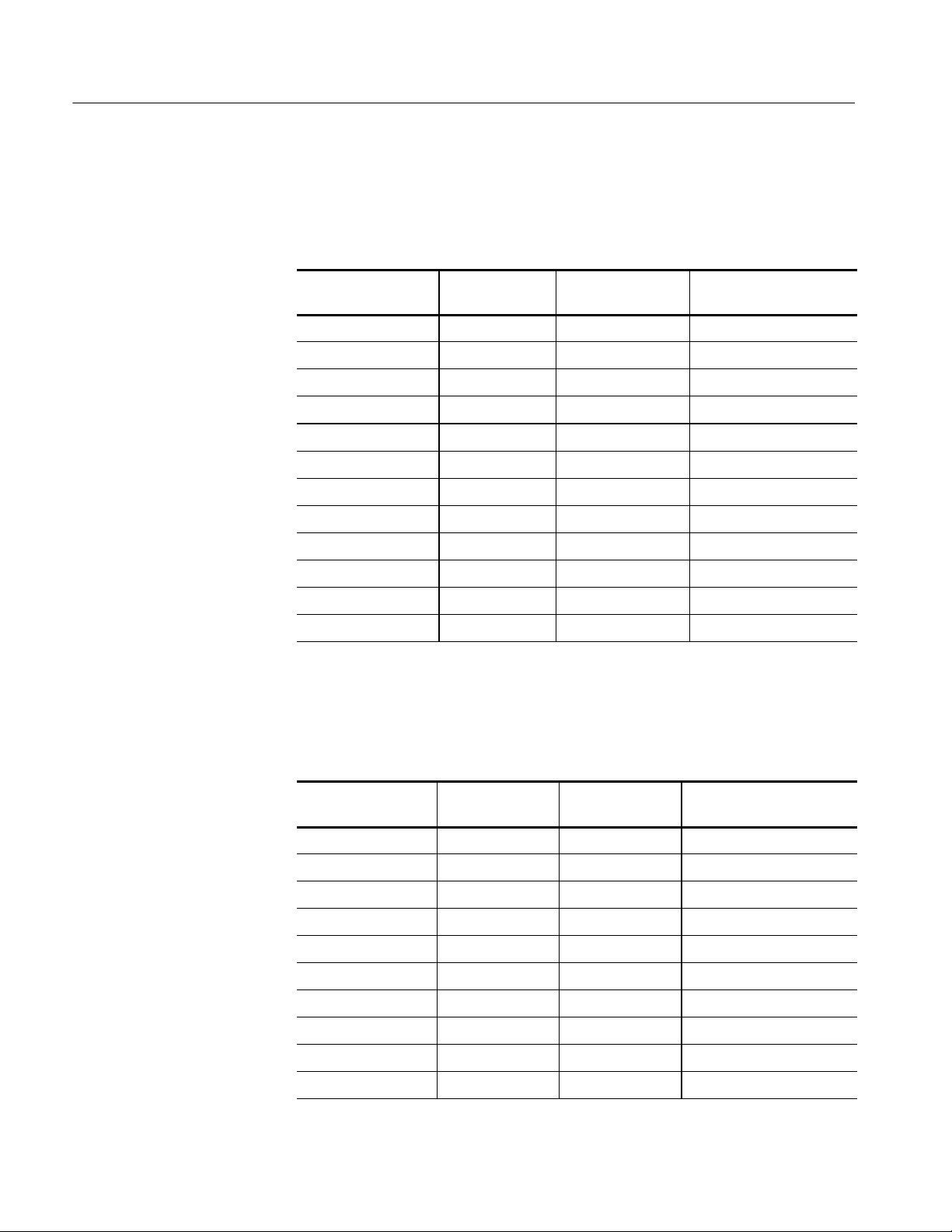
Table 2--1: Electrical specifications for the target system
Characteristics Requirements
DC power requirements
Voltage, V
Current, V
Common clock rate Maximum 133 MHz
Common clock capture
Window 839 ps
T
su
T
hd
Source Synchronous capture (DBI enabled)
Window 887 ps
T
su
T
hd
Source Synchronous capture (DBI disabled)
Window 976 ps
T
su
T
hd
cc
REF
1.2 V ᐔ5%
I maximum <20 mA, I typical <1 mA
630 ps
209 ps
345 ps
526 ps
450 ps
526 ps
Table 2--2: Electrical specifications for the AC input to the preprocessor unit
Characteristic Description
Input Voltage rating 100 -- 240 VAC CAT II
Input Frequency Rating 50 -- 60 Hz
Input Current Rating 6.0 A maximum
TMSSN1 478 Pin Socket Hardware Support
2--5
Page 48

Specifications
Table 2--3: BCLK timing and electrical specifications
Characteristics Minimum Maximum Units Notes
Vin(lo) min V
Vin(hi) max V
+300 mV V
REF
--300 mV V
REF
Duty Cycle 25 75 %
t
lh
t
hl
1.25 ns Monotonically increasing
1.25 ns Monotonically decreasing
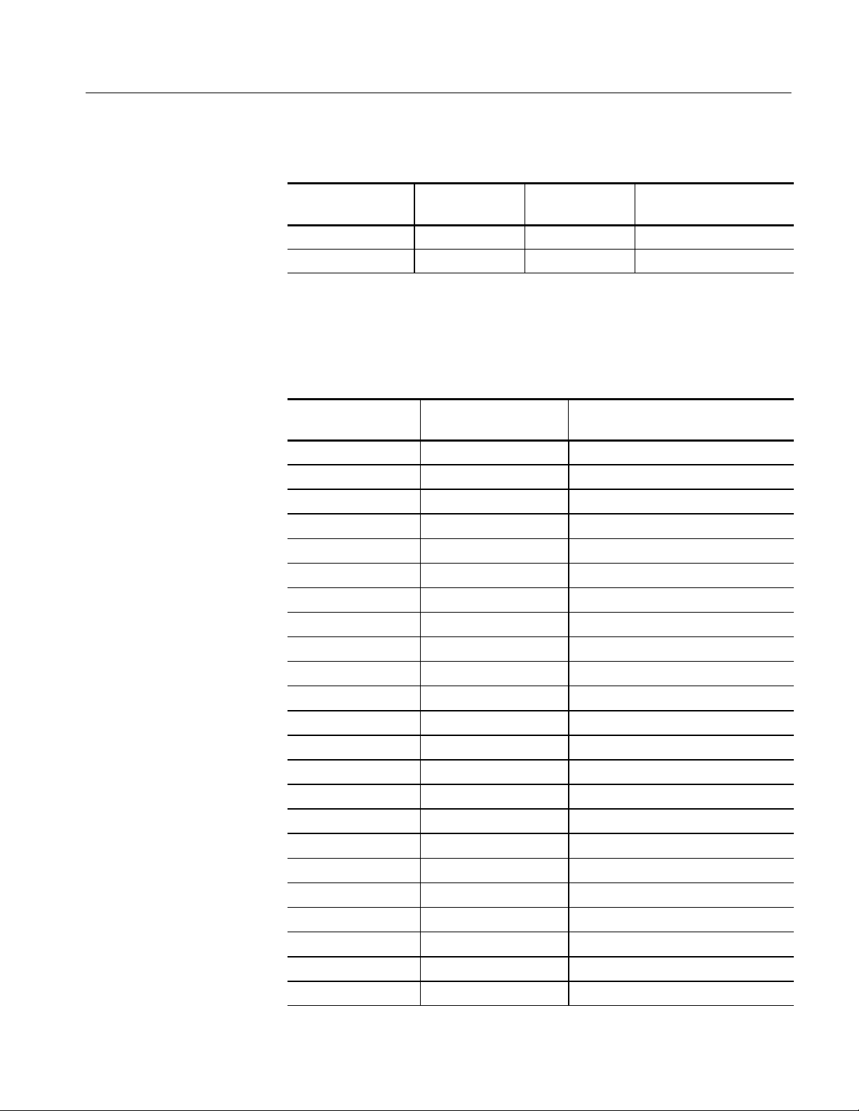
Table 2--4: Environmental specifications
Characteristic
1
Description
Temperature
Maximum operating +50° C (+122° F)
2
Minimum operating 0° C (+32° F)
Nonoperating -- 5 5 ° Cto+75° C(--67° to +167° F)
Humidity 10 to 95% relative humidity, noncondensing
Altitude
Operating 3 km (10,000 ft) maximum
Nonoperating 15 km (50,000 ft) maximum
Electrostatic immunity The probe adapter is static sensitive
Required airflow clearances
(preprocessor unit)
Sides 2in(5.08cm)
Back 3in(7.62cm)
1
Designed to meet Tektronix standard 062-2847-00 class 5.
2
Not to exceed microprocessor thermal considerations. Customer supplied cooling
might be required across the CPU.
2--6
TMSSN1 478 Pin Socket Hardware Support
Page 49
Table 2--5: Certifications and compliances
g
gyp
Category Standard or description
Specifications
EC Declaration of Conformity -Low Voltage
U.S. Nationally Recognized
Testing Laboratory Listing
Canadian Certification CAN/CSA C22.2 No. 1010.1 Safety requirements for electrical equipment for measurement,
Additional Compliance UL3111-1 Standard for electrical measuring and test equipment.
Installation (Overvoltage)
Category Descriptions
Pollution Degree A measure of the contaminates that could occur in the environment around and within a product.
Equipment Type Test and measuring
Safety Class Class 1 (as defined in IEC 61010-1, Annex H) -- grounded product
Overvoltage Category Overvoltage Category II (as defined in IEC 61010-1, Annex J)
Pollution Degree Descriptions Pollution Degree 2 (as defined in IEC 61010-1). Note: Rated for indoor use only.
Compliance was demonstrated to the following specification as listed in the Official Journal of the
European Communities:
Low Voltage Directive 73/23/EEC, amended by 93/68/EEC
EN 61010-1/A2:1995 Safety requirements for electrical equipment for measurement
control and laboratory use.
UL3111-1 Standard for electrical measuring and test equipment.
control, and laboratory use.
CAN/CSA C22.2 No. 1010.2.031:1994
Particular requirements for hand-held probe assemblies for electrical
measurement and test equipment.
Terminals on this product may have different installation (overvoltage) category designations. The
installation categories are:
CAT III Distribution-level mains (usually permanently connected). Equipment at this level is
typically in a fixed industrial location.
CAT II Local-level mains (wall sockets). Equipment at this level includes appliances, portable
tools, and similar products. Equipment is usually cord-connected.
CAT I Secondary (signal level) or battery operated circuits of electronic equipment.
Typically the internal environment inside a product is considered to be the same as the external.
Products should be used only in the environment for which they are rated.
Pollution Degree 1 No pollution or only dry, nonconductive pollution occurs. Products in
this category are generally encapsulated, hermetically sealed, or
located in clean rooms.
Pollution Degree 2 Normally only dry, nonconductive pollution occurs. Occasionally a
temporary conductivity that is caused by condensation must be
expected. This location is a typical office/home environment.
Temporary condensation occurs only when the product is out of
service.
Pollution Degree 3 Conductive pollution, or dry, nonconductive pollution that becomes
conductive due to condensation. These are sheltered locations
where neither temperature nor humidity is controlled. The area is
protected from direct sunshine, rain, or direct wind.
Pollution Degree 4 Pollution that generates persistent conductivity through conductive
dust, rain, or snow. Typical outdoor locations.
TMSSN1 478 Pin Socket Hardware Support
2--7
Page 50

Specifications
91.82 mm
(3.615 in)
5.28 mm
(.208 in)
Dimensions
Figure 2--6 shows the dimensions of the 478 Pin Socket probe head.
114.71 mm
(4.516 in)
Flex cable
76.20 mm
(3.000 in)
96.24 mm
(3.789 in)
59.44 mm
(2.340 in)
Figure 2--6: Dimensions of the 478 Pin Socket probe head
2--8
Pin A1
Heat sink removed to show
Pin A1 and board hole
location
TMSSN1 478 Pin Socket Hardware Support
Page 51
Specifications
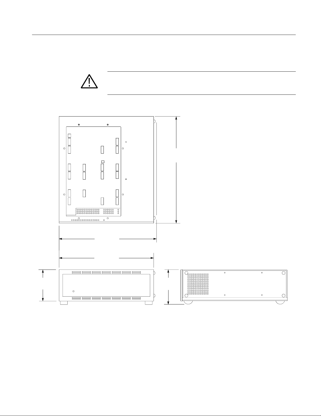
Figure 2--7 shows the dimensions of the preprocessor unit.
CAUTION. T o prevent damage to the circuitry in the prepr ocessor unit, you must
observe the r equir ed clearances in Table 2--4 on page 2--6 (clearances are not shown
in Figure 2--7).
474.32 mm
(18.674 in)
425.45 mm
(16.750 in)
420.37 mm
(16.550 in)
139.70 mm
(5.500 in)
Figure 2--7: Dimensions of the preprocessor unit
160.27 mm
(6.310 in)
TMSSN1 478 Pin Socket Hardware Support
2--9
Page 52

Specifications
2--10
TMSSN1 478 Pin Socket Hardware Support
Page 53

Reference
Page 54

Page 55

Reference: Channel Assignment Tables
This section contains channel assignments and external probing tables for the
TMSSN1 478 Pin Socket probe adapter.
Channel Assignments
Channel assignments, shown in Tables 3--3 through 3--14, use the following
conventions:
H A pound sign (#) following a signal name indicates an active low signal.
H All signals are required by the support unless indicated otherwise.
H Channels are shown starting with the most significant bit (MSB) descending
to the least significant bit (LSB).
H Signals with the prefix “M_” are on the master module, with the prefix “S_”
are on the slave module, and with the prefix “S2_” are on the Slave 2
module.
The term Master module refers to the middle module of a 3-wide merge. The
term Slave module refers to the module in the higher numbered slot than the
master module. The term Slave 2 module refers to the module in the lower
numbered slot than the master module.
Figure 3- 1: Configuration of the master, slave, and slave 2, modules
TMSSN1 478 Pin Socket Hardware Support
Slave 2 Master Slave
3- 1
Page 56
Reference: Channel Assignment Tables
Table 3--1 lists the channel assignments for the Clock group and the corresponding support channel.
Table 3- 1: Clock channel assignments
Logic analyzer
acquisition channel
M_Clock:3 Clock BCLK BCLK
M_Clock:2 Data A03 -- -- --
M_Clock:1 Data EXF0 REQ1
M_Clock:0 Data REQb0 REQ4
S_Clock:3 Data D0_DBI2 DSTBP3
S_Clock:2 Data D1_DBI3 A30
S_Clock:1 Data D3_DBI3 D35
S_Clock:0 Data D2_DBI3 DSTBP2
S2_Clock:3 Data D0_DBI1 (not available)
S2_Clock:2 Data D1_DBI0 (not available)
S2_Clock:1 Data D3_DBI0 (not available)
S2_Clock:0 Data D2_DBI0 (not available)
Clock, Qual, or
Data
IA32G7 support
channel name
IA32G7_T support
channel name
Table 3--2 lists the channel assignments for the Qualifier group and the corresponding support channel.
3- 2
Table 3- 2: Qualifier channel assignments
Logic analyzer
acquisition channel
M_Clock:3 Clock BCLK BCLK
M_Clock:2 Data A03 -- -- --
M_Clock:1 Data EXF0 REQ1
M_Clock:0 Data REQb0 REQ4
S_Clock:3 Data D0_DBI2 DSTBP3
S_Clock:2 Data D1_DBI3 A30
S_Clock:1 Data D3_DBI3 D35
S_Clock:0 Data D2_DBI3 DSTBP2
S2_Clock:3 Data D0_DBI1 (not avail able)
S2_Clock:2 Data D1_DBI0 (not avail able)
Clock, Qual, or
Data
IA32G7 support
channel name
IA32G7_T support
channel name
TMSSN1 478 Pin Socket Hardware Support
Page 57
Reference: Channel Assignment Tables
Table 3- 2: Qualifier channel assignments (cont.)
Logic analyzer
acquisition channel
S2_Clock:1 Data D3_DBI0 (not avail able)
S2_Clock:0 Data D2_DBI0 (not avail able)
Clock, Qual, or
Data
IA32G7 support
channel name
IA32G7_T support
channel name
Table 3--3 lists the channel assignments for the Address group and the corresponding support channel.
Table 3- 3: Master Module 32-channel Address assignments
Logic analyzer
acquisition channel
M_A3:7 REQb4 REQ4
M_A3:6 EXF1 REQ3
M_A3:5 EXF3 REQ2
M_A3:4 BE1 A04
M_A3:3 EXF2 A07
M_A3:2 BE7 ADSTB0
M_A3:1 BE5 A11
IA32G7 support
channel name
IA32G7_T support
channel name
M_A3:0 BE2 A15
M_A2:7 BE6 A10
M_A2:6 ATTR0 A12
M_A2:5 DID5 A20
M_A2:4 ATTR4 A19
M_A2:3 ATTR7 A28
M_A2:2 ATTR1 -- -- --
M_A2:1 ATTR3 -- -- --
M_A2:0 DID6 -- -- --
M_A1:7 REQb3 REQ1
M_A1:6 REQb1 REQ0
M_A1:5 EXF4 A06
M_A1:4 REQb2 A03
M_A1:3 DID7 A09
M_A1:2 BE0 A05
M_A1:1 BE3 A08
TMSSN1 478 Pin Socket Hardware Support
3- 3
Page 58

Reference: Channel Assignment Tables
Table 3- 3: Master Module 32-channel Address assignments (cont.)
Logic analyzer
acquisition channel
M_A1:0 DID0 A16
M_A0:7 BE4 A13
M_A0:6 DID4 A14
M_A0:5 DID3 A24
M_A0:4 ATTR2 A21
M_A0:3 ATTR6 -- -- --
M_A0:2 DID2 -- -- --
M_A0:1 ATTR5 -- -- --
M_A0:0 DID1 -- -- --
IA32G7 support
channel name
IA32G7_T support
channel name
Table 3--4 lists the channel assignments for the Data group and the corresponding
support channel.
Table 3- 4: Master Module 32-channel Data assignments
Logic analyzer
acquisition channel
M_D3:7 REQA4 -- -- --
IA32G7 support
channel name
IA32G7_T support
channel name
M_D3:6 A04 -- -- --
M_D3:5 A06 D00
M_D3:4 A09 D01
M_D3:3 A05 D06
M_D3:2 A15 DSTBN0
M_D3:1 A13 -- -- --
M_D3:0 A10 D12
M_D2:7 A14 D15
M_D2:6 A24 D10
M_D2:5 A21 D14
M_D2:4 A28 D05
M_D2:3 A31 DBI0
M_D2:2 A25 -- -- --
M_D2:1 A27 -- -- --
M_D2:0 A22 -- -- --
3- 4
TMSSN1 478 Pin Socket Hardware Support
Page 59

Reference: Channel Assignment Tables
Table 3- 4: Master Module 32-channel Data assignments (cont.)
Logic analyzer
acquisition channel
M_D1:7 REQa3 -- -- --
M_D1:6 REQa1 -- -- --
M_D1:5 A07 D02
M_D1:4 REQa2 D03
M_D1:3 A23 D09
M_D1:2 A08 -- -- --
M_D1:1 A11 D07
M_D1:0 A16 D08
M_D0:7 A12 D13
M_D0:6 A20 D11
M_D0:5 A19 DP0
M_D0:4 A26 D04
M_D0:3 A30 -- -- --
M_D0:2 A18 -- -- --
M_D0:1 A29 -- -- --
IA32G7 support
channel name
IA32G7_T support
channel name
M_D0:0 A17 GND
Table 3--5 lists the channel assignments for the Control group and the corresponding support channel.
Table 3- 5: Master Module 32-channel Control assignments
Logic analyzer
acquisition channel
M_C3:7 BPM2 FERR
M_C3:6 SLP SMI
M_C3:5 BINIT A20M
M_C3:4 Reserved LINT0
M_C3:3 Reserved HITM
M_C3:2 Reserved HIT
M_C3:1 Reserved RS2
M_C3:0 Reserved LOCK
IA32G7 support
channel name
IA32G7_T support
channel name
TMSSN1 478 Pin Socket Hardware Support
3- 5
Page 60

Reference: Channel Assignment Tables
Table 3- 5: Master Module 32-channel Control assignments (cont.)
Logic analyzer
acquisition channel
M_C2:7 Reserved BR0
M_C2:6 Reserved RESET
M_C2:5 Reserved THERMTRIP
M_C2:4 TRACK_ER_D Reserved
M_C2:3 SNOOP_D AP1
M_C2:2 RSVD1_D -- -- --
M_C2:1 INIT -- -- --
M_C2:0 RSP -- -- --
M_C1:7 BPM5 IGNNE
M_C1:6 BPM1 BPRI
M_C1:5 AP0 -- -- --
M_C1:4 GND DEFER
M_C1:3 A20M RS0
M_C1:2 DP0 BNR
M_C1:1 DP1 RS1
IA32G7 support
channel name
IA32G7_T support
channel name
M_C1:0 DP2 LINT1
M_C0:7 DP3 DBSY
M_C0:6 DBSY TRDY
M_C0:5 ADS PROCHOT
M_C0:4 HITM Reserved
M_C0:3 BPM4 -- -- --
M_C0:2 MCERR -- -- --
M_C0:1 BPM0 -- -- --
M_C0:0 IERR -- -- --
3- 6
TMSSN1 478 Pin Socket Hardware Support
Page 61

Reference: Channel Assignment Tables
Table 3--6 lists the channel assignments for the Extend group and the corresponding support channel.
Table 3- 6: Master Module 32-channel Extend assignments
Logic analyzer
acquisition channel
M_E3:7 IGNNE -- -- --
M_E3:6 FERR D21
M_E3:5 DRDY -- -- --
M_E3:4 LINT0 -- -- --
M_E3:3 RS0 DP1
M_E3:2 HIT D20
M_E3:1 RS2 -- -- --
M_E3:0 LINT1 DSTBN1
M_E2:7 BR0 D31
M_E2:6 TRDY D16
M_E2:5 THERMTRIP D24
M_E2:4 Reserved D30
M_E2:3 A35 -- -- --
M_E2:2 A34 -- -- --
M_E2:1 A33 -- -- --
IA32G7 support
channel name
IA32G7_T support
channel name
M_E2:0 A32 -- -- --
M_E1:7 SMI D23
M_E1:6 BPRI DBI1
M_E1:5 Reserved D17
M_E1:4 DEFER -- -- --
M_E1:3 BNR D22
M_E1:2 RS1 D25
M_E1:1 LOCK D19
M_E1:0 BPM3 D18
M_E0:7 PROCHOT D26
M_E0:6 AP1 D29
M_E0:5 STPCLK D28
M_E0:4 Reserved D27
M_E0:3 Ab35 -- -- --
TMSSN1 478 Pin Socket Hardware Support
3- 7
Page 62

Reference: Channel Assignment Tables
Table 3- 6: Master Module 32-channel Extend assignments (cont.)
Logic analyzer
acquisition channel
M_E0:2 Ab34 -- -- --
M_E0:1 Ab33 -- -- --
M_E0:0 Ab32 -- -- --
IA32G7 support
channel name
IA32G7_T support
channel name
Table 3--7 lists the channel assignments for the Address group and the corresponding support channel.
Table 3- 7: Slave Module 32-channel Address assignments
Logic analyzer
acquisition channel
S_A3:7 D2_D52 -- -- --
S_A3:6 D2_D48 -- -- --
S_A3:5 D2_D49 D37
S_A3:4 D2_D50 D33
S_A3:3 D2_D51 DP2
IA32G7 support
channel name
IA32G7_T support
channel name
S_A3:2 D2_D53 DSTBN2
S_A3:1 D2_D55 -- -- --
S_A3:0 D2_D57 DBI2
S_A2:7 D2_D60 D41
S_A2:6 D2_D62 D43
S_A2:5 D2_D58 D40
S_A2:4 D2_D56 D44
S_A2:3 D2_D61 -- -- --
S_A2:2 D2_D63 -- -- --
S_A2:1 D2_D54 -- -- --
S_A2:0 D2_D59 -- -- --
S_A1:7 D3_D52 -- -- --
S_A1:6 D3_D48 -- -- --
S_A1:5 D3_D49 D35
S_A1:4 D3_D50 D32
S_A1:3 D3_D51 D38
3- 8
TMSSN1 478 Pin Socket Hardware Support
Page 63

Reference: Channel Assignment Tables
Table 3- 7: Slave Module 32-channel Address assignments (cont.)
Logic analyzer
acquisition channel
S_A1:2 D3_D53 D39
S_A1:1 D3_D55 D36
S_A1:0 D3_D57 D34
S_A0:7 D3_D60 D42
S_A0:6 D3_D62 D47
S_A0:5 D3_D58 D46
S_A0:4 D3_D56 D45
S_A0:3 D3_D61 -- -- --
S_A0:2 D3_D63 -- -- --
S_A0:1 D3_D54 -- -- --
S_A0:0 D3_D59 -- -- --
IA32G7 support
channel name
IA32G7_T support
channel name
Table 3--8 lists the channel assignments for the Data group and the corresponding
support channel.
Table 3- 8: Slave Module 32-channel Data assignments
Logic analyzer
acquisition channel
S_D3:7 D0_D52 A26
S_D3:6 D0_D48 A31
S_D3:5 D0_D49 A25
S_D3:4 D0_D50 A17
S_D3:3 D0_D54 A22
S_D3:2 D0_D51 A23
S_D3:1 D0_D53 A29
S_D3:0 D0_D55 A35
S_D2:7 D0_D57 -- -- --
S_D2:6 D0_D60 -- -- --
S_D2:5 D0_D62 -- -- --
S_D2:4 D0_D59 -- -- --
S_D2:3 D0_D56 -- -- --
IA32G7 support
channel name
IA32G7_T support
channel name
TMSSN1 478 Pin Socket Hardware Support
3- 9
Page 64

Reference: Channel Assignment Tables
Table 3- 8: Slave Module 32-channel Data assignments (cont.)
Logic analyzer
acquisition channel
S_D2:2 D0_D63 -- -- --
S_D2:1 D0_D61 -- -- --
S_D2:0 D0_D58 -- -- --
S_D1:7 D1_D52 A30
S_D1:6 D1_D48 A18
S_D1:5 D1_D49 ADSTB1
S_D1:4 D1_D50 A32
S_D1:3 D1_D54 A27
S_D1:2 D1_D51 A33
S_D1:1 D1_D53 A34
S_D1:0 D1_D55 ADS
S_D0:7 D1_D57 -- -- --
S_D0:6 D1_D60 -- -- --
S_D0:5 D1_D62 -- -- --
S_D0:4 D1_D59 -- -- --
IA32G7 support
channel name
IA32G7_T support
channel name
S_D0:3 D1_D56 -- -- --
S_D0:2 D1_D63 -- -- --
S_D0:1 D1_D61 -- -- --
S_D0:0 D1_D58 -- -- --
Table 3--9 lists the channel assignments for the Control group and the corresponding support channel.
Table 3- 9: Slave Module 32-channel Control assignments
Logic analyzer
acquisition channel
S_C3:7 D0_D35 -- -- --
S_C3:6 D0_D40 -- -- --
S_C3:5 D0_D37 D52
S_C3:4 D0_D33 D49
S_C3:3 D0_D38 D50
IA32G7 support
channel name
IA32G7_T support
channel name
3- 10
TMSSN1 478 Pin Socket Hardware Support
Page 65

Reference: Channel Assignment Tables
Table 3- 9: Slave Module 32-channel Control assignments (cont.)
Logic analyzer
acquisition channel
S_C3:2 D0_D32 -- -- --
S_C3:1 D0_D39 DSTBN3
S_C3:0 D0_D34 D55
S_C2:7 D0_D41 D60
S_C2:6 D0_D36 D59
S_C2:5 D0_D42 D56
S_C2:4 D0_D43 DP3
S_C2:3 D0_D47 -- -- --
S_C2:2 D0_D44 -- -- --
S_C2:1 D0_D46 -- -- --
S_C2:0 D0_D45 -- -- --
S_C1:7 D1_D35 -- -- --
S_C1:6 D1_D40 -- -- --
S_C1:5 D1_D37 D48
S_C1:4 D1_D33 DBI3
IA32G7 support
channel name
IA32G7_T support
channel name
S_C1:3 D1_D38 D51
S_C1:2 D1_D32 D54
S_C1:1 D1_D39 D53
S_C1:0 D1_D34 D57
S_C0:7 D1_D41 D58
S_C0:6 D1_D36 D62
S_C0:5 D1_D42 D63
S_C0:4 D1_D43 D61
S_C0:3 D1_D47 -- -- --
S_C0:2 D1_D44 -- -- --
S_C0:1 D1_D46 -- -- --
S_C0:0 D1_D45 -- -- --
TMSSN1 478 Pin Socket Hardware Support
3- 11
Page 66

Reference: Channel Assignment Tables
Table 3--10 lists the channel assignments for the Extend group and the corresponding support channel.
Table 3- 10: Slave Module 32-channel Extend assignments
Logic analyzer
acquisition channel
S_E3:7 D2_D35 STPCLK
S_E3:6 D2_D32 BPM4
S_E3:5 D2_D37 BPM0
S_E3:4 D2_D33 Reserved
S_E3:3 D2_D38 BPM5
S_E3:2 D2_D39 IERR
S_E3:1 D2_D34 MCERR
S_E3:0 D2_D41 -- -- --
S_E2:7 D2_D36 BPM1
S_E2:6 D2_D42 -- -- --
S_E2:5 D2_D43 -- -- --
S_E2:4 D2_D47 -- -- --
S_E2:3 D2_D40 -- -- --
S_E2:2 D2_D44 -- -- --
S_E2:1 D2_D45 -- -- --
IA32G7 support
channel name
IA32G7_T support
channel name
3- 12
S_E2:0 D2_D46 -- -- --
S_E1:7 D3_D35 -- -- --
S_E1:6 D3_D32 INIT
S_E1:5 D3_D37 BPM3
S_E1:4 D3_D33 BINIT
S_E1:3 D3_D38 RSP
S_E1:2 D3_D39 AP0
S_E1:1 D3_D34 -- -- --
S_E1:0 D3_D41 BPM2
S_E0:7 D3_D36 -- -- --
S_E0:6 D3_D42 -- -- --
S_E0:5 D3_D43 -- -- --
S_E0:4 D3_D47 -- -- --
S_E0:3 D3_D40 -- -- --
TMSSN1 478 Pin Socket Hardware Support
Page 67

Reference: Channel Assignment Tables
Table 3- 10: Slave Module 32-channel Extend assignments (cont.)
Logic analyzer
acquisition channel
S_E0:2 D3_D44 -- -- --
S_E0:1 D3_D45 -- -- --
S_E0:0 D3_D46 -- -- --
IA32G7 support
channel name
IA32G7_T support
channel name
Table 3--11 lists the channel assignments for the Address group and the
corresponding support channel.
Table 3- 11: Slave 2 Module 32-channel Address assignments
Logic analyzer
acquisition channel
S2_A3:7 D2_D01 (not available)
S2_A3:6 D2_D03 (not available)
S2_A3:5 D2_D09 (not available)
S2_A3:4 D2_D06 (not available)
S2_A3:3 D2_D02 (not available)
IA32G7 support
channel name
IA32G7_T support
channel name
S2_A3:2 D2_D07 (not available)
S2_A3:1 D2_D15 (not available)
S2_A3:0 D2_D12 (not available)
S2_A2:7 D2_D08 (not available)
S2_A2:6 D2_D13 (not available)
S2_A2:5 D2_D14 (not available)
S2_A2:4 D2_D10 (not available)
S2_A2:3 D2_D00 (not available)
S2_A2:2 D2_D04 (not available)
S2_A2:1 D2_D11 (not available)
S2_A2:0 D2_D05 (not available)
S2_A1:7 D3_D01 (not available)
S2_A1:6 D3_D03 (not available)
S2_A1:5 D3_D09 (not available)
S2_A1:4 D3_D06 (not available)
S2_A1:3 D3_D02 (not available)
TMSSN1 478 Pin Socket Hardware Support
3- 13
Page 68
Reference: Channel Assignment Tables
Table 3- 11: Slave 2 Module 32-channel Address assignments (cont.)
Logic analyzer
acquisition channel
S2_A1:2 D3_D07 (not available)
S2_A1:1 D3_D15 (not available)
S2_A1:0 D3_D12 (not available)
S2_A0:7 D3_D08 (not available)
S2_A0:6 D3_D13 (not available)
S2_A0:5 D3_D14 (not available)
S2_A0:4 D3_D10 (not available)
S2_A0:3 D3_D00 (not available)
S2_A0:2 D3_D04 (not available)
S2_A0:1 D3_D11 (not available)
S2_A0:0 D3_D05 (not available)
IA32G7 support
channel name
IA32G7_T support
channel name
Table 3--12 lists the channel assignments for the Data group and the corresponding support channel.
Table 3- 12: Slave 2 Module 32-channel Data assignments
Logic analyzer
acquisition channel
S2_D3:7 D0_D00 (not available)
S2_D3:6 D0_D02 (not available)
S2_D3:5 D0_D03 (not available)
S2_D3:4 D0_D09 (not available)
S2_D3:3 D0_D06 (not available)
S2_D3:2 D0_D07 (not available)
S2_D3:1 D0_D15 (not available)
S2_D3:0 D0_D12 (not available)
S2_D2:7 D0_D08 (not available)
S2_D2:6 D0_D13 (not available)
S2_D2:5 D0_D14 (not available)
S2_D2:4 D0_D10 (not available)
S2_D2:3 D0_D01 (not available)
IA32G7 support
channel name
IA32G7_T support
channel name
3- 14
TMSSN1 478 Pin Socket Hardware Support
Page 69

Reference: Channel Assignment Tables
Table 3- 12: Slave 2 Module 32-channel Data assignments (cont.)
Logic analyzer
acquisition channel
S2_D2:2 D0_D04 (not available)
S2_D2:1 D0_D11 (not available)
S2_D2:0 D0_D05 (not available)
S2_D1:7 D1_D00 (not available)
S2_D1:6 D1_D02 (not available)
S2_D1:5 D1_D03 (not available)
S2_D1:4 D1_D09 (not available)
S2_D1:3 D1_D06 (not available)
S2_D1:2 D1_D07 (not available)
S2_D1:1 D1_D15 (not available)
S2_D1:0 D1_D12 (not available)
S2_D0:7 D1_D08 (not available)
S2_D0:6 D1_D13 (not available)
S2_D0:5 D1_D14 (not available)
S2_D0:4 D1_D10 (not available)
IA32G7 support
channel name
IA32G7_T support
channel name
S2_D0:3 D1_D01 (not available)
S2_D0:2 D1_D04 (not available)
S2_D0:1 D1_D11 (not available)
S2_D0:0 D1_D05 (not available)
Table 3--13 lists the channel assignments for the Control group and the corresponding support channel.
Table 3- 13: Slave 2 Module 32-channel Control assignments
Logic analyzer
acquisition channel
S2_C3:7 D0_D23 (not available)
S2_C3:6 D0_D16 (not available)
S2_C3:5 D0_D29 (not available)
S2_C3:4 D0_D21 (not available)
S2_C3:3 D0_D22 (not available)
IA32G7 support
channel name
IA32G7_T support
channel name
TMSSN1 478 Pin Socket Hardware Support
3- 15
Page 70

Reference: Channel Assignment Tables
Table 3- 13: Slave 2 Module 32-channel Control assignments (cont.)
Logic analyzer
acquisition channel
S2_C3:2 D0_D17 (not available)
S2_C3:1 D0_D20 (not available)
S2_C3:0 D0_D19 (not available)
S2_C2:7 D0_D18 (not available)
S2_C2:6 D0_D25 (not available)
S2_C2:5 D0_D31 (not available)
S2_C2:4 D0_D26 (not available)
S2_C2:3 D0_D28 (not available)
S2_C2:2 D0_D24 (not available)
S2_C2:1 D0_D30 (not available)
S2_C2:0 D0_D27 (not available)
S2_C1:7 D1_D23 (not available)
S2_C1:6 D1_D16 (not available)
S2_C1:5 D1_D29 (not available)
S2_C1:4 D1_D21 (not available)
IA32G7 support
channel name
IA32G7_T support
channel name
S2_C1:3 D1_D22 (not available)
S2_C1:2 D1_D17 (not available)
S2_C1:1 D1_D20 (not available)
S2_C1:0 D1_D19 (not available)
S2_C0:7 D1_D18 (not available)
S2_C0:6 D1_D25 (not available)
S2_C0:5 D1_D31 (not available)
S2_C0:4 D1_D26 (not available)
S2_C0:3 D1_D28 (not available)
S2_C0:2 D1_D24 (not available)
S2_C0:1 D1_D30 (not available)
S2_C0:0 D1_D27 (not available)
3- 16
TMSSN1 478 Pin Socket Hardware Support
Page 71

Reference: Channel Assignment Tables
Table 3--14 lists the channel assignments for the Extended group and the
corresponding support channel.
Table 3- 14: Slave 2 Module 32-channel Extended assignments
Logic analyzer
acquisition channel
S2_E3:7 D2_D23 (not available)
S2_E3:6 D2_D29 (not available)
S2_E3:5 D2_D28 (not available)
S2_E3:4 D2_D21 (not available)
S2_E3:3 D2_D22 (not available)
S2_E3:2 D2_D17 (not available)
S2_E3:1 D2_D20 (not available)
S2_E3:0 D2_D19 (not available)
S2_E2:7 D2_D18 (not available)
S2_E2:6 D2_D25 (not available)
S2_E2:5 D2_D31 (not available)
S2_E2:4 D2_D26 (not available)
S2_E2:3 D2_D16 (not available)
S2_E2:2 D2_D24 (not available)
S2_E2:1 D2_D30 (not available)
IA32G7 support
channel name
IA32G7_T support
channel name
S2_E2:0 D2_D27 (not available)
S2_E1:7 D3_D23 (not available)
S2_E1:6 D3_D29 (not available)
S2_E1:5 D3_D28 (not available)
S2_E1:4 D3_D21 (not available)
S2_E1:3 D3_D22 (not available)
S2_E1:2 D3_D17 (not available)
S2_E1:1 D3_D20 (not available)
S2_E1:0 D3_D19 (not available)
S2_E0:7 D3_D18 (not available)
S2_E0:6 D3_D25 (not available)
S2_E0:5 D3_D31 (not available)
S2_E0:4 D3_D26 (not available)
TMSSN1 478 Pin Socket Hardware Support
3- 17
Page 72
Reference: Channel Assignment Tables
Table 3- 14: Slave 2 Module 32-channel Extended assignments (cont.)
Logic analyzer
acquisition channel
S2_E0:3 D3_D16 (not available)
S2_E0:2 D3_D24 (not available)
S2_E0:1 D3_D30 (not available)
S2_E0:0 D3_D27 (not available)
IA32G7 support
channel name
IA32G7_T support
channel name
Table 3--15 lists signals not available on the probe adapter. If you want access to
these signals you must find another way to probe them.
Table 3- 15: Signals not available on the
probe adapter
Signal name
BSEL[1:0]
COMP[1:0]
GLTREF[3:0]
ODTEN#
PWRGOOD
SKTOCC#
TESTHI[10:0]
THERMDA
TMERMDC
VCC
VCCA
VCCIOPLL
VCCSENSE
VCCVIDPRG
VID[4:0]
VSSA
VSSSENSE
3- 18
TMSSN1 478 Pin Socket Hardware Support
Page 73

WARNING
The following servicing instructions are for use only by qualified personnel. To
avoid injury, do not perform any servicing other than that stated in the operating
instructions unless you are qualified to do so. Refer to all safety summaries before
performing any service.
Page 74

Page 75

Maintenance
Page 76

Page 77

Maintenance
Fuses
This section contains fuse information for the TMSSN1 478 Pin Socket probe
adapter.
The TMSSN1 478 Pin Socket probe adapter, consists of the probe head, cables,
and preprocessor unit, and does not require scheduled or periodic maintenance.
However, to keep good electrical contact and efficient heat dissipation, keep the
probe adapter free of dirt, dust, and contaminants. When not in use, store the
probe adapter in the original shipping bags and shipping boxes (see Storage on
page 1--19).
WARNING. To prevent personal injury or damage to the preprocessor unit, there
are no operator serviceable parts inside the cover of the preprocessor unit. Refer
servicing of internal parts in the preprocessor unit to Tektronix authorized
personnel only.
There are four fuses in the preprocessor unit:
H Logic board:
F1, Part Number 159--0059--00; 5A, 125 V Fast blow
F2 and F3, Part Number 159--5015--00; 10 A, 125 V Fast blow
H Power Supply (1)
(1) Part Number 159--5015--00; 10 A, 125 V Fast blow
TMSSN1 478 Pin Socket Hardware Support
4- 1
Page 78

Maintence
4- 2
TMSSN1 478 Pin Socket Hardware Support
Page 79

Removal and Installation Procedures
This section contains removal and installation procedures for the cables in the
TMSSN1 478 Pin Socket probe adapter.
WARNING. To prevent personal injury or damage to the preprocessor unit, cables
and fans should be replaced by qualified service personnel only.
There are no operator serviceable parts inside the cover of the preprocessor unit.
Refer servicing of internal parts in the preprocessor unit to Tektronix authorized
personnel only.
Removing the Cables
The information in this section is designed for use by qualified service personnel.
Read the Safety Summary at the front of this manual before attempting any
procedures in this section.
Tools Required
Removing Cables from
the Preprocessor Unit
Following are the tools required for the removal procedures:
H POZIDRIV screwdriver (PZ2) to remove the bottom cover
H Flat-bladed screwdriver to loosen the thumbscrews on the paddle boards, and
remove the snap rivets from the fan guards and probe head cables)
Please read the following general instructions before removing parts.
You may need to remove the cables from the preprocessor unit to exchange the
probe head or to replace the cables. Follow these steps to remove the cables.
CAUTION. Static discharge can damage the microprocessor, the probe adapter,
the probes, and the module. To prevent static damage, you must handle components only in a static-free environment.
Always wear a grounding wrist strap, heel strap, or similar device while
handling the microprocessor and probe adapter.
TMSSN1 478 Pin Socket Hardware Support
4--3
Page 80
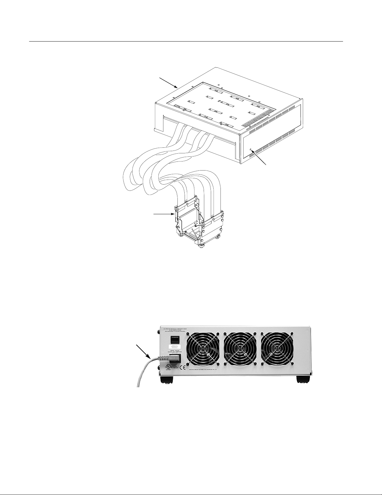
Removal and Installation Procedures
Preprocessor unit
Power light
Probe head
cables
Probe head
Figure 4--1: Probe head and preprocessor unit
1. Power off the preprocessor unit. The power switch is located on the back of
the preprocessor unit (see Figure 4--2).
2. Unplug the AC power cord from the preprocessor unit.
AC Power cord
Figure 4--2: Remove AC power cord
3. If necessary, remove the P6434 probes, and turn the preprocessor unit over
onto its topside (see Figure 4--3). To disconnect the P6434 probes, refer to
the P6434 Mass Termination Probe manual, Tektronix part number
070-9793-XX, for more information on mechanical specifications.
4--4
TMSSN1 478 Pin Socket Hardware Support
Page 81

Removal and Installation Procedures
Screws (6)
Figure 4--3: Remove the attaching screws
WARNING. To prevent serious injury or death, check that the power cord is
disconnected from the line voltage source.
4. With a POZIDRIV screwdriver (PZ2), remove the screws and bottom cover
from the preprocessor unit, and set them aside (see Figure 4--3 and 4--4).
Bottom
cover
The preprocessor unit may
show paddle boards from
other probe adapters.
Warning!
High Voltage
Power
supply
Figure 4--4: Remove the bottom cover
TMSSN1 478 Pin Socket Hardware Support
4--5
Page 82
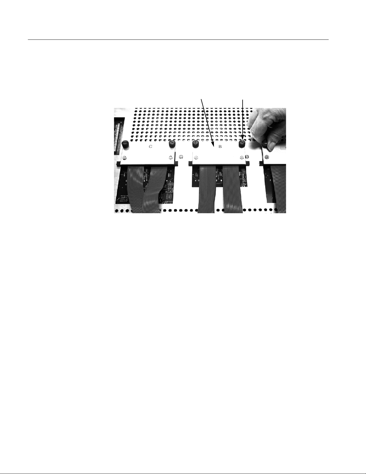
Removal and Installation Procedures
w
5. With a flat-bladed screwdriver, loosen the captive thumb screws from the
Logic board cover plate, and disconnect each paddle board from the bottom
of the Logic board (see Figure 4--5).
Paddle board
Captive thumb scre
Figure 4--5: Remove the cables from the logic board
4--6
TMSSN1 478 Pin Socket Hardware Support
Page 83
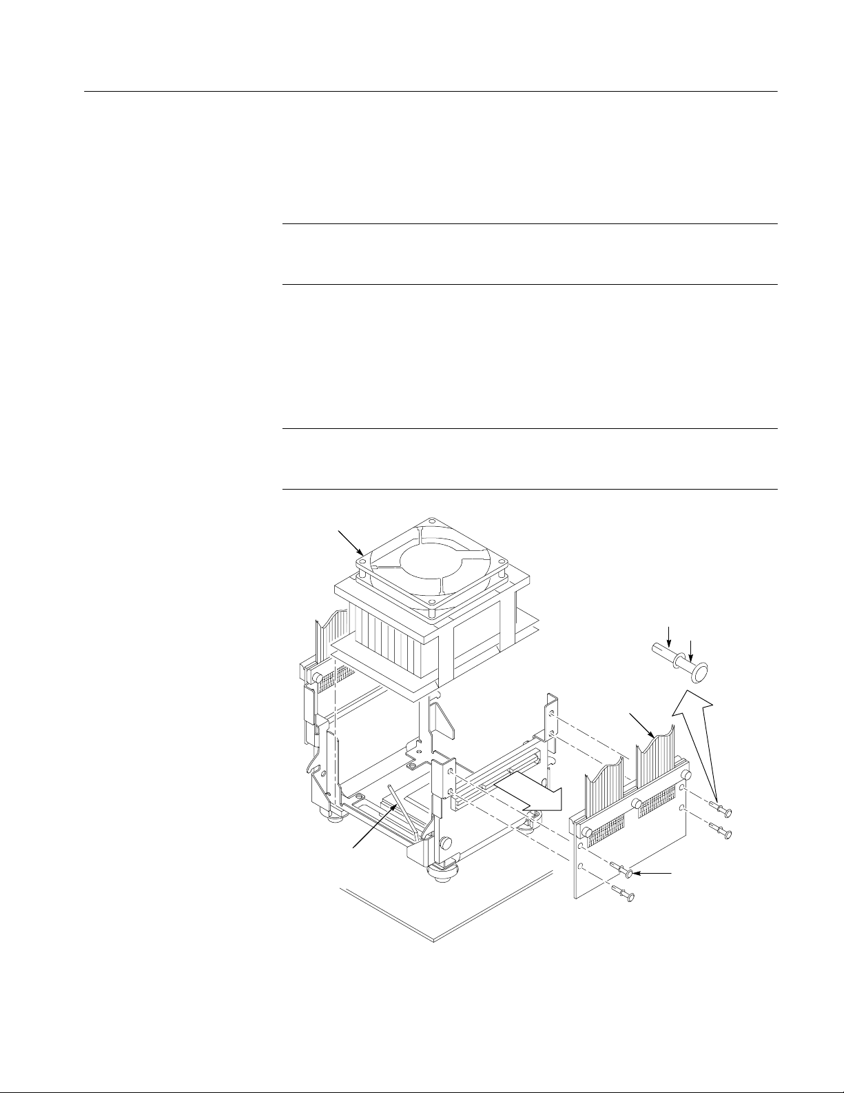
Removal and Installation Procedures
Removing the Cables
from the Probe Head
For probe head and cable exchange you do not need to disconnect the cables
from the probe head. If you need to disconnect the cables from the probe head for
other applications, continue with the following steps:
NOTE. You must remove the heat sink and fan assembly before removing the
probe head cable ends. Complete Steps 1 through 6 starting on page 1--13, and
then continue with the following steps.
1. Remove the rivets from the probe head cable end (see Figure 4--6):
a. Using a flat-bladed screwdriver, pry the rivet halfway out of the rivet
holder.
b. Remove the rivet and its holder from the probe head circuit board.
NOTE. To prevent a loose-rivet fastener, you may want to replace the rivets after
each removal and replacement operation. The rivets also become difficult to
reinsert after one use because of an expanded rivet tip.
Heat sink
and fan
Lift handle up
to deactivate
ZIF socket
Figure 4--6: Remove the cables from the probe head
Holder
Rivet
Probe head
cable end (2)
Rivet and
Holder (4)
TMSSN1 478 Pin Socket Hardware Support
4--7
Page 84
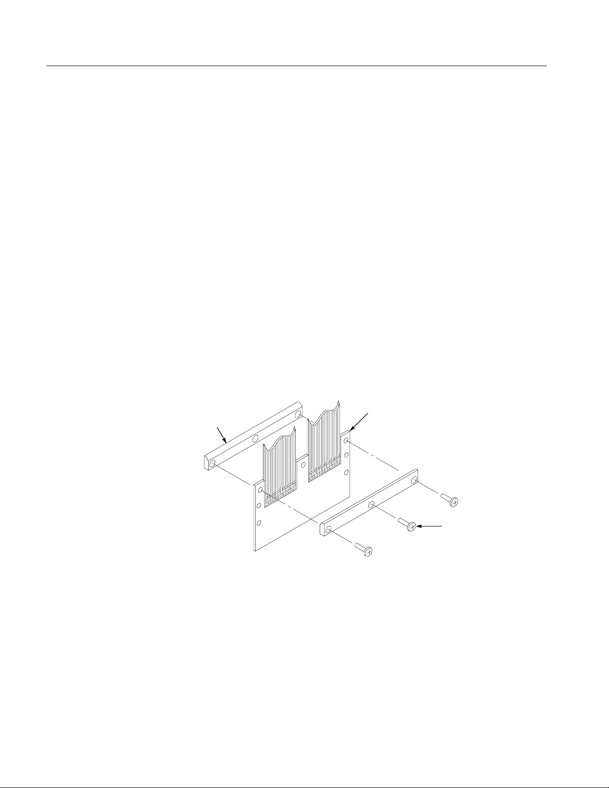
Removal and Installation Procedures
2. Repeat step 1 for the other cable.
To ship the probe head and cables, see Shipping the Probe Head and Cables on
page 4--10.
Replacing the Cables
To replace the cables between the preprocessor unit and the probe head, you must
have already completed all the previous steps (removing the cables from the
preprocessor unit and prober head) before continuing with steps 1 through 9:
Probe-head cable end.
1. Remove the screws from the strain-relief bars on the probe-head cable end
2. Discard the old cable and retrieve the new cable.
3. Align the strain-relief bar holes and the probe-head cable-end holes.
(see Figure 4--7). Set the strain-relief bars and screws aside.
4. With the new cable between the two strain-relief bars, reattach the screws to
the strain-relief bars (see Figure 4--7) using a flat-bladed screwdriver.
Strain relief
bracket
Probe head end
the cable
Screw (3)
Figure 4--7: Probe-head cable end
4--8
TMSSN1 478 Pin Socket Hardware Support
Page 85
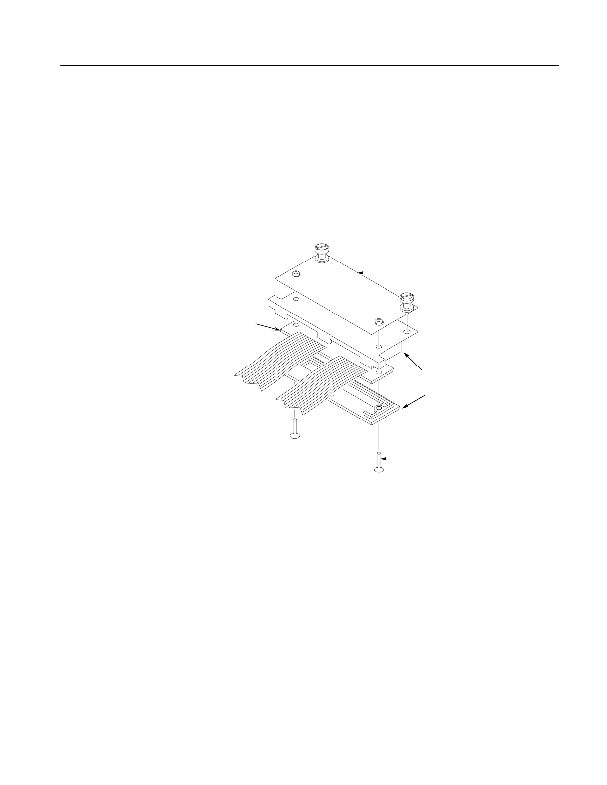
Removal and Installation Procedures
Preprocessor cable end.
5. Remove the screws that hold the black plastic housing to the plate (see
Figure 4--8). Set the screws aside.
6. Snap open the black plastic housing holding the cable. Set the housings
aside.
7. Place the preprocessor end of the new cable between the housing covers and
snap the housings closed around the cable.
Plate
Preprocessor
end of the
cable
Figure 4--8: Preprocessor cable end
Black plastic
housing (2)
Screw (2)
TMSSN1 478 Pin Socket Hardware Support
4--9
Page 86

Removal and Installation Procedures
NOTE. Check that all four corners on the black plastic housing are squarely
seated in each corner (see Figure 4--9).
Squarely seated
Check for gap
Figure 4--9: Check corners
8. Using the screws, attach the black plastic housing to the plate.
9. Repeat steps 1 through 9 for the other cable.
To ship the cables and probe head, see Shipping the Probe Head and Cableson
page 4--10. To reconnect the cables to the preprocessor and probe head, see
Reconnecting the Cables to the Probe Head on page 4--15.
Shipping the Probe Head and Cables
To commercially transport the TMSSN1 478 Pin Socket probe head assembly,
package as follows:
1. Use a double-walled, corrugated cardboard shipping carton with an inside
diameter of three inches (7.62 cm) larger on each side and top than the probe
head assembly.
2. If you are shipping the probe head assembly to a Tektronix service center for
Warranty service, attach a tag to the probe head showing the following:
4--10
H Owner’s name and address
H Name of a person who can be contacted
H Probe adapter type and serial number
TMSSN1 478 Pin Socket Hardware Support
Page 87
Removal and Installation Procedures
H Description of the problem
3. Using antistatic nongenerating tape, tape the probe head pin-protector board
onto the pin header.
4. Wrap pink poly (antistatic) bubble wrap around the probe head.
5. Wrap the three paddle boards in pink poly (antistatic) bubble wrap or
antistatic bags.
CAUTION. To avoid breaking the cable connections, you must handle the cables
carefully to reduce stress on the cable connections. If you need to fold a cable,
use a minimum of a 0.25 in (0.64 cm) radius at the fold.
6. Place the probe head and cables in the cardboard carton on top of the packing
material.
7. Tightly pack dunnage or urethane foam between the card board carton and
the probe adapter (allowing three inches (7.62 cm) on each side) to cushion
the probe adapter.
8. Close and tape the cardboard carton.
TMSSN1 478 Pin Socket Hardware Support
4--11
Page 88
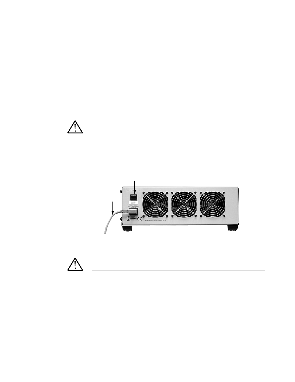
Removal and Installation Procedures
Reinstalling the Cables
You may need to reinstall the cables on the preprocessor unit. Follow these steps:
Reinstalling the Cables on
the Preprocessor Unit
1. Power off the preprocessor unit and disconnect the power cord (see Figure
4--10 for power switch and power cord locations). Check that the P6434
probes are removed from the top of the preprocessor unit before turning it
over.
2. Turn the preprocessor unit over.
CAUTION. Static discharge can damage the microprocessor, the probe adapter,
the probes, and the module. To prevent static damage, you must handle components only in a static-free environment.
Always wear a grounding wrist strap, heel strap, or similar device while
handling the microprocessor and probe adapter.
Power switch
Power cord
4--12
Figure 4--10: Power switch location
WARNING. To prevent serious injury or death, disconnect the power cord from the
preprocessor unit.
3. With a POZIDRIVR screwdriver (PZ2), remove the bottom cover.
4. Dress the cables through the notched side of the preprocessor unit (see
Figure 4--11).
TMSSN1 478 Pin Socket Hardware Support
Page 89

The preprocessor unit may
show paddle boards from
other probe adapters.
Removal and Installation Procedures
Power
supply
Warning!
High voltage
Figure 4--11: Dress the cables through the side opening
5. Connect each cable housing to the corresponding location (A-A, B-B, C-C)
on the bottom of the Logic board. Secure the cable housings to the Logic
board cover plate using the captive thumb screws (see Figure 4--12).
Figure 4--12: Attach the cables to the logic board cover plate
6. With a POZIDRIVR screwdriver (PZ2), attach the bottom cover to the
preprocessor unit using the attaching screws (see Figure 4--13).
TMSSN1 478 Pin Socket Hardware Support
4--13
Page 90

Removal and Installation Procedures
Screws (6)
Figure 4--13: Attach the bottom cover
7. Turn the preprocessor unit over.
8. Reconnect the P6434 probes (see pages 1--10 through 1--14) to the top of the
preprocessor unit.
9. Plug the AC power cord into the back of the preprocessor unit.
4--14
TMSSN1 478 Pin Socket Hardware Support
Page 91

Removal and Installation Procedures
Reconnecting the Cables
on the Probe Head
If you need to reconnect the cables to the probe head continue with the following
steps:
1. Align the rivet holes on the probe-head end of the cable with the probe head.
2. Attach the rivets:
a. Pull the center rivet pin halfway out of the rivet assembly.
b. Press the rivet assembly through the rivet holes of the probe head and
circuit board.
Heat sink
and fan
Holder
Rivet
Probe head
cable end (2)
Lift handle up
to deactivate
ZIF socket
Figure 4--14: Place the heat sink on the probe head
3. Repeat steps 1 and 2 for the other cable.
NOTE. To prevent a lose-rivet fastener, you may want to replace the rivets after
each removal and replacement operation. The rivets also become difficult to
reinsert after one use because of an expanded rivet tip.
TMSSN1 478 Pin Socket Hardware Support
Rivet and
Holder (4)
4--15
Page 92

Removal and Installation Procedures
After reconnecting the cables, you may need to complete Steps 9 through 12
starting on page 1--10 to replace the microprocessor, and heat sink and fan
assembly.
Removing and Instaling a Fan
You may need to remove and install a fan in the preprocessor unit for repair
purposes. To replace a fan follow these steps:
If all three fans are not working, check that the power cord is connected to the
preprocessor unit or the electrical outlet. If the power cord is connected, contact a
Tektronix service representative.
CAUTION. Static discharge can damage the microprocessor, the probe adapter,
the probes, and the module. To prevent static damage, you must handle components only in a static-free environment.
Always wear a grounding wrist strap, heel strap, or similar device while
handling the microprocessor and probe adapter.
1. Power off the preprocessor unit. The power switch is located on the back of
the preprocessor unit (see Figure 4--15). To disconnect the P6434 probes,
refer to the P6434 Mass Termination Probe manual, Tektronix part number
070-9793-XX, for more information on mechanical specifications.
2. Unplug the AC power cord from the preprocessor unit.
Power switch
Unplug the AC
Power cord
Figure 4--15: Power switch and AC power cord locations
WARNING. To prevent serious injury or death, check that the power cord is
disconnected from the preprocessor unit.
4--16
3. Turn the preprocessor unit over, and remove the screws (see Figure 4--16)
and bottom cover from the preprocessor unit. Set the bottom cover aside.
TMSSN1 478 Pin Socket Hardware Support
Page 93

Screws (6)
Figure 4--16: Remove the attaching screws
Removal and Installation Procedures
Removing a Fan
Deflector shield
screws (4)
Power supply
Warning High voltage
The preprocessor unit may
show paddle boards from
other probe adapters.
Fan connector
Figure 4--17: Remove the bottom cover
4. If you are replacing the fan behind the power supply, remove the screws and
deflector shield from the power supply shield. If not, skip to step 5.
5. Disconnect the fan connector from the logic-board connector by pressing the
release tab on the fan connector.
TMSSN1 478 Pin Socket Hardware Support
4--17
Page 94

Removal and Installation Procedures
6. Cut the two cable ties that bundle the fan wires together.
Tweezer (push gently)
Fan connector housing
Square hole
Pin connector
Figure 4--18: Remove the pin connectors
7. Remove the fan pin from the fan connector housing (at the logic board
connector side) by following steps a through c:
a. Using a dental pick (or tweezer point), place the tool point in the top
square hole of the fan connector housing.
b. Gently press and slide the pin a little with the tool point. This small
movement releases the pin from the fan connector housing.
CAUTION. To prevent damage to the fan pin and the fan connector, do not gouge
at the pin with the tool point.
c. Gently slide the pin from the fan connector housing using your hand. The
pin removal procedure may take a couple of tries, unless you are
experienced with pin removal.
8. Remove the rivets, fan guard, and fan from the preprocessor unit. When
removing the rivets, pull the rivet center pin halfway out and then remove the
whole rivet assembly.
4--18
TMSSN1 478 Pin Socket Hardware Support
Page 95

Removal and Installation Procedures
NOTE. To prevent a loose-rivet fastener, you may want to replace the rivets after
each removal and replacement operation. The rivets also become difficult to
reinsert after one use because of an expanded rivet tip.
9. Remove the fan from the preprocessor unit.
Holder
Rivet
Rivet and fan guard
Fan guard
mounting ring
Installing a Fan
Figure 4--19: Back of the preprocessor unit
10. Position the writing on the fan hub to point toward the back of the preproces-
sor unit.
11. With the rivet pin pulled halfway out of the rivet assembly, insert the rivet
assembly through the fan grill mounting ring, preprocessor hole, and fan hole
(see Figure 4--19).
12. Press the rivet pin into the rivet assembly.
13. Repeat steps 11 and 12 for the other rivet installations.
14. Slide and snap the fan pin into the fan connector housing. Gently pull on the
fan pin to insure the fan pin has seated in the fan connector.
TMSSN1 478 Pin Socket Hardware Support
4--19
Page 96
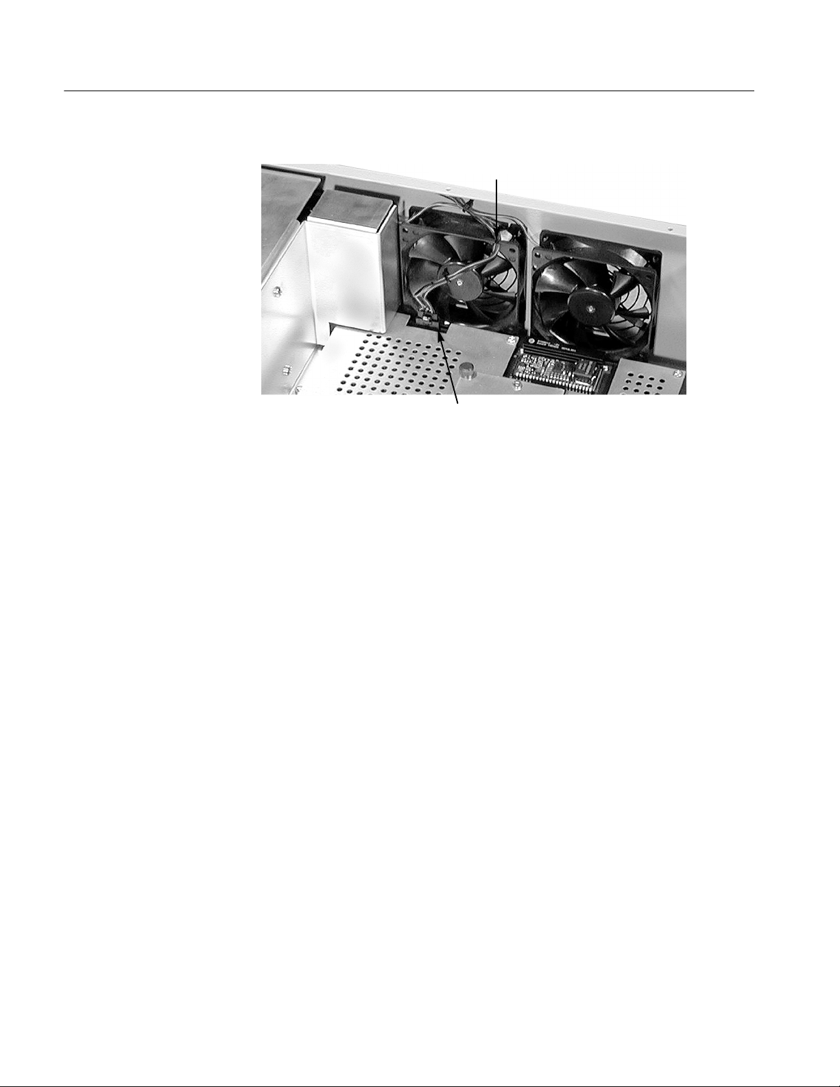
Removal and Installation Procedures
Figure 4--20: Location of fan connector
Dress the fan wires through
the center fan notch
Fan connecter
15. Connect the fan connector to the logic-board connector (see Figure 4--17 on
page 4--17).
16. Dress the fan wire over the top of the fans and through the notch on the top
of the center fan (see Figure 4--20).
17. Attach two cable ties to the bundle of fan wires securing the fan wires in
place.
18. Attach the bottom cover to the preprocessor unit using the attaching screws
(see Figure 4--16 on page 4--17).
19. Turn the preprocessor unit right-side up.
20. Plug the AC power cord into the preprocessor unit.
21. Power on the preprocessor unit and check that the fans are rotating.
If the replaced fan is not working:
H Check that the fan pin is seated properly in the fan connector housing.
H Check that the fan connector has snapped in place.
4--20
TMSSN1 478 Pin Socket Hardware Support
Page 97

Replaceable Parts List
Page 98

Page 99

Replaceable Parts List
This section contains a list of the replaceable components or modules for the
TMSSN1 478 Pin Socket Hardware Support package.
Parts Ordering Information
Replacement parts are available through your local Tektronix field office or
representative.
Changes to Tektronix products are sometimes made to accommodate improved
components as they become available and to give you the benefit of the latest
improvements. Therefore, when ordering parts, it is important to include the
following information in your order:
H Part number
H Instrument type or model number
H Instrument serial number
H Instrument modification number, if applicable
Module Servicing
If you order a part that has been replaced with a different or improved part, your
local Tektronix field office or representative will contact you concerning any
change in part number.
Modules can be serviced by selecting one of the following three options. Contact
your local Tektronix service center or representative for repair assistance.
Module Exchange. In some cases you may exchange your module for a remanufactured module. These modules cost significantly less than new modules and
meet the same factory specifications. For more information about the module
exchange program, call 1-800-833-9200. Outside North America, contact a
Tektronix sales office or distributor; see the Tektronix web site for a list of
offices: www.tektronix.com.
Module Repair and Return. You may ship your module to us for repair, after which
we will return it to you.
New Modules. You may purchase replacement modules in the same way as other
replacement parts.
TMSSN1 478 Pin Socket Hardware Support
5--1
Page 100

Replaceable Parts List
Using the Replaceable Parts List
This section contains a list of the mechanical and/or electrical components that
are replaceable for the TMSSN1 478 Pin Socket Hardware Support package. Use
this list to identify and order replacement parts. The following table describes
each column in the parts list.
Parts list column descriptions
Column Column name Description
1 Figure & index number Items in this section are referenced by figure and index numbers to the exploded view illustrations
that follow.
2 Tektronix part number Use this part number when ordering replacement parts from Tektronix.
3 and 4 Serial number Column three indicates the serial number at which the part was first effective. Column four
indicates the serial number at which the part was discontinued. No entry indicates the part is
good for all serial numbers.
5 Qty This indicates the quantity of parts used.
6 Name & description An item name is separated from the description by a colon (:). Because of space limitations, an
item name may sometimes appear as incomplete. Use the U.S. Federal Catalog handbook H6-1
for further item name identification.
7 Mfr. code This indicates the code of the actual manufacturer of the part.
8 Mfr. part number This indicates the actual manufacturer’s or vendor’s part number.
Abbreviations
Mfr. Code to Manufacturer
Cross Index
Abbreviations conform to American National Standard ANSI Y1.1--1972.
The table titled Manufacturers Cross Index shows codes, names, and addresses of
manufacturers or vendors of components listed in the parts list.
5--2
TMSSN1 478 Pin Socket Hardware Support
 Loading...