

Page 1

Instruction Manual
TMSPGC
PGA370 Single-Ended/Differential Clock
Hardware Support
071-0803-01
www.tektronix.com
Page 2

Copyright © Tektronix, Inc. All rights reserved. Licensed software products are owned by Tektronix or its suppliers and
are protected by United States copyright laws and international treaty provisions.
Use, duplication, or disclosure by the Government is subject to restrictions as set forth in subparagraph (c)(1)(ii) of the
Rights in Technical Data and Computer Software clause at DFARS 252.227-7013, or subparagraphs (c)(1) and (2) of the
Commercial Computer Software -- Restricted Rights clause at FAR 52.227-19, as applicable.
Tektronix products are covered by U.S. and fore ign patents, issued and pending. Information in this publication superce des
that in all previously published material. Specifications and price change privileges reserved.
Tektronix, Inc., P.O. Box 500, Beaverton, OR 97077
TEKTRONIX and TEK are registered trademarks of Tektronix, Inc.
Page 3

WARRANTY
Tektronix warrants that the media on which this software product is furnished and the encoding of the programs on
the media will be free from defects in materials and workmanship for a period of three (3) months from the date of
shipment. If a medium or encoding proves defective during the warranty period, Tektronix will provide a
replacement in exchange for the defective medium. Except as to the media on which this software product is
furnished, this softwa re product i s provided “as is” without warranty of any ki nd, e ither express or implied.
Tektronix does not warrant that the functions containe d in this software product will meet Customer’s
requirements or that the operation of the programs will be uninterrupted or error-free.
In order to obtai n servic e under thi s warranty, Customer must notify Tektronix of the defect before the expiration
of the warranty period. If Tektronix is unable to provide a replacement that is free from defects in materials and
workmanship within a reasonable time thereafter, Customer may terminate the license for this software product
and return this software product and any associated materials for credit or refund.
THIS WARRANTY IS GIVEN BY TEKTRONIX IN LIEU OF ANY OTHER W ARRANTIES, EXPRESS
OR IMPLIED. TEKTRONIX AND ITS VENDORS DISCLAIM ANY IMPLIED WARRANTIES OF
MERCHANTABILITY OR FITNESS FOR A PARTICULAR PURPOSE. TEKTRONIX’
RESPONSIBILITY TO REPLACE DEFECTIVE MEDIA OR REFUND CUSTOMER’S PAYMENT IS
THE SOLE AND EXCLUSIVE REMEDY PROVIDED TO THE CUSTOMER FOR BREACH OF THIS
WARRANTY. TEKTRONIX AND ITS VENDORS WILL NOT BE LIABLE FOR ANY INDIRECT,
SPECIAL, INCIDENTAL, OR CONSEQUENTIAL DAMAGES IRRESPECTIVE OF WHETHER
TEKTRONIX OR THE VENDOR HAS ADVANCE NOTICE OF THE POSSIBILITY OF SUCH
DAMAGES.
Page 4

Page 5

Table of Contents
Getting Started
General Safety Summary v...................................
Service Safety Summary vii....................................
Preface ix...................................................
Manual Conventions ix..............................................
Contacting Tektronix x.............................................
Getting Started 1--1............................................
Support Package Description 1--1.......................................
Support Software Compatibility 1--1.....................................
Logic Analyzer Configuration 1--1.....................................
Requirements and Restrictions 1--2......................................
Labeling P6434 Probes 1--2............................................
Assembling the Probe Adapter 1--4......................................
Connecting the Logic Analyzer to a Target System 1--6.....................
Configuring the Probe Adapter 1--11.....................................
MODE Jumper 1--11...............................................
FREQUENCY Jumper 1--11........................................
Alternate Connections 1--12............................................
Applying and Removing Power 1--14....................................
Reference
Specifications
Maintenance
Replaceable Parts List
Index
Reference: Channel Tables 2--1..................................
Channel Assignments 2--1.............................................
Specifications 3--1.............................................
Circuit Description 3--1...............................................
Probe Adapter Loading Diagrams 3--2...................................
Specification Tables 3--4..............................................
Maintenance 4--1..............................................
Replacing The Fuse 4--1..............................................
Replaceable Parts List 5--1......................................
Parts Ordering Information 5--1.........................................
Using the Replaceable Parts List 5--1....................................
TMSPGC PGA-370 SE/DIFF Clk Hardware Support
i
Page 6

Table of Contents
List of Figures
Figure 1--1: Seating the 190-pin Mictor connector 1--4...............
Figure 1--2: Attaching the Logic board to the Interposer board 1--5....
Figure 1--3: TMSPGC probe adapter protective sockets 1--7..........
Figure 1--4: Inserting a protective socket into the ZIF socket 1--7......
Figure 1--5: Inserting the probe adapter into the socket 1--8..........
Figure 1--6: Placing the PGA370 microprocessor into the probe adapter . . .
1--9
Figure 1--7: Connecting a probe to the probe adapter 1--10............
Figure 1--8: Jumper locations on the TMSPGC probe adapter 1--11....
Figure 1--9: JTAG port locations on the probe adapter 1--13...........
Figure 1--10: APIC pin locations on the probe adapter 1--14...........
Figure 1--11: Location of the power jack 1--15.......................
Figure 3--1: BCLK and BCLK# signals with active loads 3--2.........
Figure 3--2: AGTL signals with active loads, except RESET# 3--2.....
Figure 3--3: CMOS signals with active loads, plus RESET# 3--3.......
Figure 3--4: JTAG signals without active loads 3--3.................
Figure 3--5: Equivalent circuit for the P6434 probe 3--4..............
Figure 3--6: Dimensions of the TMSPGC probe adapter 3--8.........
Figure 4--1: Fuse location on the TMSPGC probe adapter 4--1........
Figure 5--1: Exploded view of the TMSPGC PGA370 probe adapter 5--6
TMSPGC PGA-370 SE/DIFF Clk Hardware Support
ii
Page 7

List of Tables
Table of Contents
Table 1--1: DBRESET information 1--12...........................
Table 1--2: APIC information 1--13...............................
Table 2--1: Clock channels assignments 2--1.......................
Table 2--2: Qualifier channel assignments 2--1.....................
Table 2--3: Master A channel assignments 2--2.....................
Table 2--4: Master D channel assignments 2--3.....................
Table 2--5: Master C channel assignments 2--4....................
Table 2--6: Slave A channel assignments 2--5......................
Table 2--7: Slave D channel assignments 2--7......................
Table 2--8: Slave C channel assignments 2--8......................
Table 3--1: Lossy delay line values 3--4...........................
Table 3--2: Electrical specifications for the target system 3--5........
T able 3--3: BCLK and BCLK# electrical specifications,
differential clock 3--5.....................................
T able 3--4: BCLK and CLKREF electrical specifications,
single-ended clock 3--5....................................
T able 3--5: AGTL electrical specifications 3--6....................
T able 3--6: CMOS electrical specifications (1.5 V) 3--6............
T able 3--7: Electrical specifications for the AC adapter 3--6.........
T able 3--8: Environmental specifications 3--7.....................
TMSPGC PGA-370 SE/DIFF Clk Hardware Support
iii
Page 8

Table of Contents
TMSPGC PGA-370 SE/DIFF Clk Hardware Support
iv
Page 9

General Safety Summary
Review the following safety precautions to avoid injury and prevent damage to
this product or any products connected to it. To avoid potential hazards, use this
product only as specified.
Only qualified personnel should perform service procedures.
While using this product, you may need to access other parts of the system. Read
the General Safety Summary in other system manuals for warnings and cautions
related to operating the system.
ToAvoidFireor
Personal Injury
Use Proper Power Cord. Use only the power cord specified for this product and
certified for the country of use.
Connect and Disconnect Properly. Connect the probe output to the measurement
instrument before connecting the probe to the circuit under test. Disconnect the
probe input and the probe ground from the circuit under test before disconnecting
the probe from the measurement instrument.
Observe All Terminal Ratings. To avoid fire or shock hazard, observe all ratings
and markings on the product. Consult the product manual for further ratings
information before making connections to the product.
Do not apply a potential to any terminal, including the common terminal, that
exceeds the maximum rating of that terminal.
Use Proper AC Adapter. Use only the AC adapter specified for this product.
Do Not Operate Without Covers. Do not operate this product with covers or panels
removed.
Use Proper Fuse. Use only the fuse type and rating specified for this product.
Avoid Exposed Circuitry. Do not touch exposed connections and components
when power is present.
Do Not Operate With Suspected Failures. If you suspect there is damage to this
product, have it inspected by qualified service personnel.
Do Not Operate in Wet/Damp Conditions.
Do Not Operate in an Explosive Atmosphere.
Keep Product Surfaces Clean and Dry.
Provide Proper Ventilation. Refer to the manual’s installation instructions for
details on installing the product so it has proper ventilation.
TMSPGC PGA-370 SE/DIFF Clk Hardware Support
v
Page 10

General Safety Summary
Symbols and Terms
Terms in this Manual. These terms may appear in this manual:
CAUTION. Caution statements identify conditions or practices that could result in
damage to this product or other property.
Terms on the Product. These terms may appear on the product:
CAUTION indicates a hazard to property including the product.
Symbols on the Product. The following symbols may appear on the product:
CAUTION
Refer to Manual
Double
Insulated
Protective Ground
(Earth) Terminal
TMSPGC PGA-370 SE/DIFF Clk Hardware Support
vi
Page 11

Service Safety Summary
Only qualified personnel should perform service procedures. Read this Service
Safety Summary and the General Safety Summary before performing any service
procedures.
Do Not Service Alone. Do not perform internal service or adjustments of this
product unless another person capable of rendering first aid and resuscitation is
present.
Disconnect Power. To avoid electric shock, switch off the instrument power, then
disconnect the power cord from the mains power.
Use Care When Servicing With Power On. Dangerous voltages or currents may
exist in this product. Disconnect power, remove battery (if applicable), and
disconnect test leads before removing protective panels, soldering, or replacing
components.
To avoid electric shock, do not touch exposed connections.
TMSPGC PGA-370 SE/DIFF Clk Hardware Support
vii
Page 12

Service Safety Summary
viii
TMSPGC PGA-370 SE/DIFF Clk Hardware Support
Page 13

Preface
This instruction manual contains specific information about the
TMSPGC PGA370 microprocessor support package and is part of a set of
information on how to operate this product on compatible Tektronix logic
analyzers.
If you are familiar with operating microprocessor support packages on the logic
analyzer for which the TMSPGC PGA370 support was purchased, you will only
need this instruction manual to set up and run the support.
If you are not familiar with operating microprocessor support packages, you will
need to supplement this instruction manual with TMS 115 IA32G5 Software
Support manual and information on basic operations in your online help to set up
and run the support.
This manual provides detailed information on the following topics:
H Assembling and configuring the probe adapter
H Connecting the logic analyzer to the system under test
H Applying power and operating the probe adapter
Manual Conventions
This manual uses the following conventions:
H The phrase “information on basic operations” refers to basic information in
your Tektronix logic analyzer online help.
H The term Master module refers to the module in the lower-numbered slot and
the term Slave module refers to the module in the higher-numbered slot.
The portable logic analyzer has the lower numbered slots on the top and the
benchtop logic analyzer has the lower numbered slots on the left.
TMSPGC PGA-370 SE/DIFF Clk Hardware Support
ix
Page 14

Preface
Contacting Tektronix
Phone 1-800-833-9200*
Address Tektronix, Inc.
Department or name (if known)
14200 SW Karl Braun Drive
P.O. Box 500
Beaverton, OR 97077
USA
Web site www.tektronix.com
Sales support 1-800-833-9200, select option 1*
Service support 1-800-833-9200, select option 2*
Technical support Email: techsupport@tektronix.com
1-800-833-9200, select option 3*
6:00 a.m. -- 5:00 p.m. Pacific time
* This phone number is toll free in North America. After office hours, please leave a
voice mail message.
Outside North America, contact a Tektronix sales office or distributor; see the
Tektronix web site for a list of offices.
x
TMSPGC PGA-370 SE/DIFF Clk Hardware Support
Page 15

Getting Started
Page 16

Page 17

Getting Started
This section contains information on the TMSPGC PGA370 hardware support
package and connecting the logic analyzer to the target system.
Support Package Description
The TMSPGC probe adapter is nonintrusive hardware that allows the logic
analyzer to acquire data from a microprocessor in its own operating environment
with little affect on that system.
The TMSPGC probe adapter is an interposer design. The probe adapter connects
to the target system, and then, the microprocessor connects to the probe adapter.
Signals from the microprocessor-based system flow through the probe adapter
into the P6434 probes and through the probe cables to the logic analyzer.
Support Software Compatibility
The TMSPGC probe adapter requires a Tektronix microprocessor s oftware
support package. This TMSPGC probe adapter is used with the TMS 115
Software Support package.
Logic Analyzer Configuration
To use the TMSPGC PGA370 hardware support package you need a Tektronix
logic analyzer equipped with two 102-channel modules. The modules must be in
adjacent slots and merged.
References to a 204-channel module include the two 102-channel modules that
are merged and any other merged module combination of a minimum of
204-channels (for the merged combination).
You can acquire JTAG and APIC bus activity through the TMSPGC probe
adapter. Probing the APIC bus requires the TMS 801 APIC bus support package,
a third 102-channel acquisition module, and standard probes. See Alternate
Connections on page 1--12 for more details.
TMSPGC PGA-370 SE/DIFF Clk Hardware Support
1-- 1
Page 18

Getting Started
Requirements and Restrictions
CAUTION. Forced air cooling must be used to keep the microprocessor from
overheating.
You should review the general requirements and restrictions of microprocessor
support packages in the information on basic operations as they pertain to the
target system.
You should also review electrical, environmental, and mechanical specifications
in Specifications on page 3--1 as they pertain to the target system, as well as the
following descriptions of other TMSPGC PGA370 hardware support requirements and restrictions.
System Clock Rate
BCLK
AGTL
CMOS
Target System Power
The TMSPGC PGA370 microprocessor support can acquire data from the
PGA370 microprocessors operating at speeds of up to 133 MHz.
The operating clock rate specifications were measured at the time of printing.
Contact your Tektronix sales representative for current information on the fastest
devices supported.
The TMSPGC PGA370 hardware support can operate with either a low-voltage
differential clock, or with a normal voltage single-ended clock. Refer to the
BCLK specifications listed in Table 3--3 and 3--4 beginning on page 3--5, in the
Specifications chapter.
The TMSPGC PGA370 hardware support can operate with either AGTL
(1.2 volt) or AGTLT (1.5 volt) logic levels. Refer to the AGTL specifications
listed in Table 3--5 on page 3--6.
The TMSPGC PGA370 hardware support can operate with only 1.5 volt CMOS
logic levels. Refer to the CMOS specifications listed in Table on page .
Whenever you power off the target system, remove power from the probe
adapter. Refer to Applying and Removing Power on page 1--14.
Labeling P6434 Probes
1-- 2
The TMSPGC PGA370 hardware support package relies on the standard channel
mapping and labeling scheme for P6434 probes. Apply labels using the standard
method described in the P6434 Mass Termination Probe Instructions.
TMSPGC PGA-370 SE/DIFF Clk Hardware Support
Page 19

Getting Started
Signals Acquired
Signals Not Acquired
The following signals are acquired by the TMSPGC probe adapter:
A20M# BINIT# DEP[7:0]# IERR# PWRGOOD STPCLK#
A[35:3] BNR# DEFER# IGNNE# RESET# THRMTRP#
ADS# BP[3:2]# DID[7:0]# INIT# REQ[4:0] TCK
AERR# BPM[1:0]# DRDY# LOCK# RP# TDI
ATTR[7:0]# BPRI# EXF[4:0]# LINT[1:0] RSP# TDO
AP[1:0]# BREQ0# FLUSH# PICD[1:0] RS[2:0]# TMS
BE[7:0]# D[63:0] FERR# PICCLK SLP# TRST#
BERR# DBSY# HIT# PRDY# SMI# TRDY#
BCLK HITM# PREQ#
The following signals are not acquired by the TMSPGC probe adapter:
PGA370 signal name PGA370 pin number
BSEL[0] AJ33
BSEL[1] AJ31
CPUPRES# C37
NCHCTRL N37
PLL1 W33
PLL2 U33
RTTCTRL S35
SLEWCTRL E27
THRMDN AL29
THRMDP AL31
VID25mv AK36
VID[0] AL35
VID[1] AM36
VID[2] AL37
VID[3] AJ37
VTT_PWRGD AK4
TMSPGC PGA-370 SE/DIFF Clk Hardware Support
1-- 3
Page 20

Getting Started
Assembling the Probe Adapter
The probe adapter assembly consists of a Logic board, Interposer board, three
protective sockets (disassembly, timing analysis, and JTAG debugging), and
screws.
CAUTION. To prevent static discharge from damaging the microprocessor, the
probe adapter, the probes, and the module, handle components only in a
static-free environment.
Always wear a grounding wrist strap, heel strap, or similar device while
handling the microprocessor and probe adapter.
Do the following steps to assemble the probe adapter:
1. To discharge any static electricity, touch the ground connector located on the
logic analyzer. Then, before you remove the probe adapter circuit boards
from their protective bags, touch each bag to discharge stored static
electricity.
190-pin Mictor
Interposer
board
2. Align the Logic board connector pins with the Interposer board connector
pins, and press firmly to seat the board connector (see Figure 1--1). Both
connectors are polarized and only mate in one orientation.
NOTE. To ensure a reliable electrical connection between the Logic board and the
Interposer board the 190-pin Mictor connector must be completely seated at both
ends (see Figure 1--1).
Logic board
The top of the plug
is not level with the
top of receptacle
Gap
Correct
The top of the plug
is level with the top
of receptacle
No gap on
either end
Incorrect
Figure 1--1: Seating the 190-pin Mictor connector
1-- 4
TMSPGC PGA-370 SE/DIFF Clk Hardware Support
Page 21

Getting Started
3. Align the mounting brackets on the logic board with the mounting holes on
the interposer board, and attach with the provided screws (see Figure 1--2).
CAUTION. To prevent damage to the probe adapter, use the provided screws to
secure the logic board to the Interposer board.
Logic board
Screws (2)
Interposer board
Protective socket
Figure 1--2: Attaching the Logic board to the Interposer board
TMSPGC PGA-370 SE/DIFF Clk Hardware Support
1-- 5
Page 22

Getting Started
Connecting the Logic Analyzer to a Target System
Your target system must allow clearance for the probe adapter. Refer to the
dimensions on page 3--8 for the required clearances.
To connect the logic analyzer to the target system, follow these steps:
1. Power off the target system. It is not necessary to power off the logic
analyzer.
CAUTION. To prevent static discharge from damaging the microprocessor, the
probe adapter, the probes, and the acquisition module, handle the components
only in a static-free environment.
Always wear a grounding wrist strap, heel strap, or similar device while
handling the microprocessor and probe adapter.
2. Follow the procedure from the microprocessor vendor to remove the
microprocessor from the PGA370 socket on the target system.
NOTE. Do not remove the protective socket from the bottom of the probe adapter.
Do not install a protective socket without removing all existing sockets from the
target system.
3. Choose the correct protective socket (see Figure 1--3).
When using the TMSPGC probe adapter:
H Use the 363-pin protective socket only when using the JTAG port on the
TMSPGC probe adapter.
H Use the 370-pin protective socket at all other times.
1-- 6
TMSPGC PGA-370 SE/DIFF Clk Hardware Support
Page 23

Getting Started
370 pins protective socket
Black holes are missing pins
363 pins JTAG protective socket
Figure 1--3: TMSPGC probe adapter protective sockets
4. Align the A3 pin indicator on the protective socket with pin A3 of the
PGA370 protective socket on the target system.
5. Insert the protective socket into the target system as shown in Figure 1--4.
socket protective
(370 pin or 363 pin)
Pin A3
ZIF socket
Pin A3
Figure 1--4: Inserting a protective socket into the ZIF socket
TMSPGC PGA-370 SE/DIFF Clk Hardware Support
1-- 7
Page 24

Getting Started
6. Align the A3 pin indicator on the probe adapter with the A3 pin indicator on
the installed socket.
7. Insert the probe adapter into the installed socket as shown in Figure 1--5.
Logic board
1-- 8
Interposer board
Pin A3
Target system
Figure 1--5: Inserting the probe adapter into the socket
TMSPGC PGA-370 SE/DIFF Clk Hardware Support
Page 25

Getting Started
8. Insert the microprocessor into the probe adapter as shown in Figure 1--6.
PGA370
Microprocessor
Attach the P6434 probes
Pin A3
Target system
Figure 1--6: Placing the PGA370 microprocessor into the probe adapter
9. Reattach the heat sink from the target system to the probe adapter.
After you have connected the probe adapter to the target system, connect three
P6434 probes to the Master module and three P6434 probes to the Slave module.
The module in the lower-numbered slot is referred to as the Master module and
the module in the higher-numbered slot is referred to as the Slave module.
The portable logic analyzer has the lower numbered slots on the top and the
benchtop logic analyzer has the lower numbered slots on the left.
TMSPGC PGA-370 SE/DIFF Clk Hardware Support
1-- 9
Page 26

Getting Started
1. Match the A, C, and D probes from the Master module with the correspond-
ing M_A, M_C, and M_D probe connectors on the probe adapter. Align the
pin 1 indicator on the probe label with the pin 1 indicator of the connector on
the probe adapter.
CAUTION. Incorrect handling of the P6434 probe while connecting it to the probe
adapter can result in damage to the probe or to the mating connector on the
probe adapter. To avoid damaging the probe and probe adapter, always position
the probe perpendicular to the mating connector and gently connect the probe.
2. Position the probe tip perpendicular to the mating connector and gently
connect the probe (see Figure 1--7).
3. When connected, push latch releases in to set the latch on the probe .
Push in to latch after
probe is connected
Push in to latch after
probe is connected
Pin 1
Pin 1
Figure 1--7: Connecting a probe to the probe adapter
4. Match the A, C, and D probes from the Slave module with the corresponding
S_A, S_C, and S_D probe connectors on the probe adapter. Align the pin 1
indicator on the probe label with pin 1 of the connector on the probe adapter.
5. Repeat steps 2 and 3.
1-- 10
TMSPGC PGA-370 SE/DIFF Clk Hardware Support
Page 27
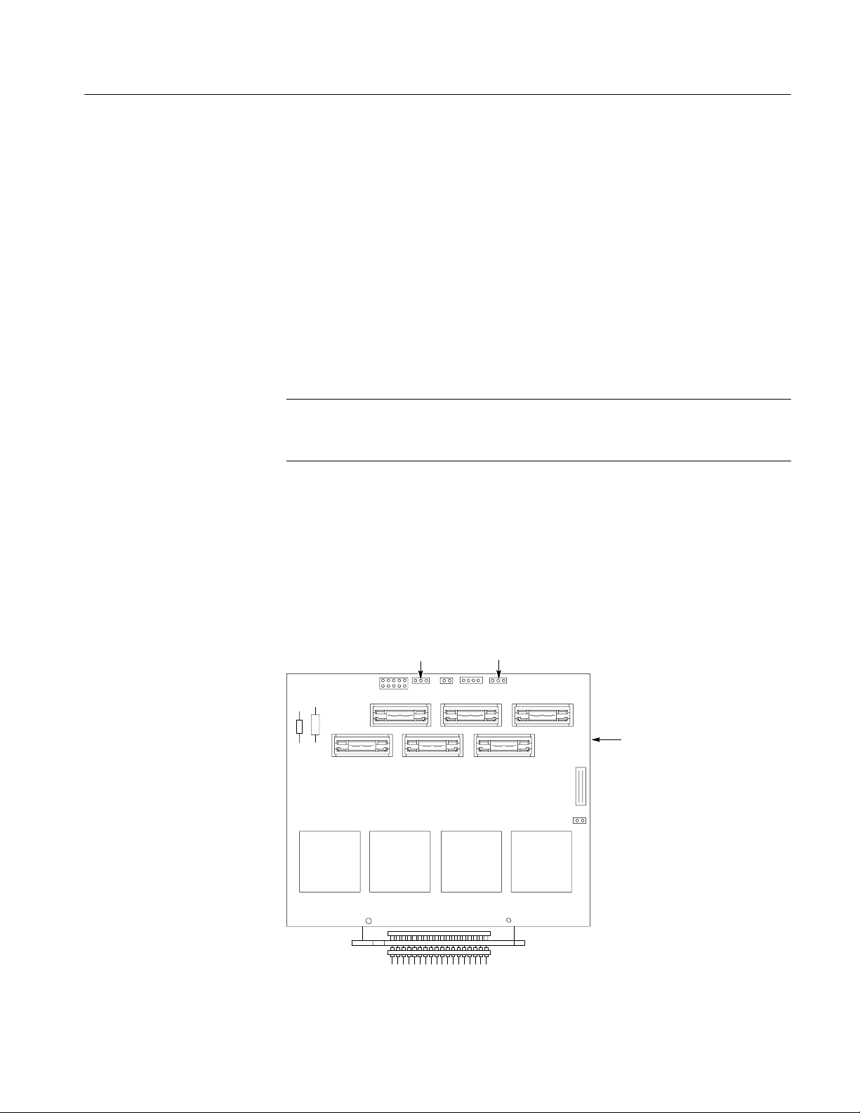
Configuring the Probe Adapter
The probe adapter uses jumpers to acquire data for disassembly or for timing
analysis. Figure 1--8 shows the location of the jumpers.
Getting Started
MODE Jumper
FREQUENCY Jumper
Place the MODE select jumper, J140, in the NORMAL position to acquire data
for disassembly (IA32G5) or synchronous timing analysis (IA32G5_T) using
Custom clocking.
Place the MODE select jumper, J140, in the TRANSPARENT position to acquire
data for asynchronous timing analysis with the IA32G5_T setup using Internal
clocking.
NOTE. Due to setup/hold requirements, the TRANSPARENT mode is not
recommended for synchronous acquisitions. All synchronous timing analysis is
done in the NORMAL mode with the IA32G5_T setup.
Place the FREQUENCY select jumper J160, in the HI position when operating
between 120 and 200 MHz. Place the FREQUENCY select jumper J160, in the
LO position when operating between 60 and 140 MHz.
Figure 1--8 shows the location of J140 and J160 on the probe adapter.
MODE
J140
Frequency
J160
Figure 1--8: Jumper locations on the TMSPGC probe adapter
TMSPGC PGA-370 SE/DIFF Clk Hardware Support
Logic board
1-- 11
Page 28

Getting Started
Alternate Connections
JTAG
The TMSPGC probe adapter logic board provides J490 as a way to connect to
JTAG debugging hardware. JTAG debugging hardware is not included with the
TMSPGC PGA370 hardware support package. Contact your microprocessor
vendor for information on how to obtain JTAG debugging hardware.
NOTE. The JTAG circuitry on the Logic board is active only when the JTAG
device is connected to J490. If the JTAG device is disconnected from J490, all
JTAG data and control lines on the logic board are tristated.
Optional System Reset. The JTAG circuitry on the Logic board does not allow
external JTAG debugging hardware to induce a system reset through the
DBRESET# signal on the JTAG port. If you need to use this feature you must
provide the connection from these pins to the target system. The following Table
1--1 lists the signals on the J590.
Table 1--1: DBRESET information
J590 Pin number JTAG signal name
1 GND
2 DBRESET#
1-- 12
Figure 1--9 shows the location of the DBRESET# and JTAG port on the logic
board of the probe adapter.
When using the JTAG port on the TMSPGC probe adapter, use the 363 pin
protective socket (see page 1--6). Use the 370 pin protective socket at all other
times.
TMSPGC PGA-370 SE/DIFF Clk Hardware Support
Page 29

Figure 1--9: JTAG port locations on the probe adapter
Getting Started
Logic board
J490
JTAG port
J590
DBRESET#
APIC
Four pins on J150 are provided to connect the TMS801 APIC bus probe adapter
to the PICCLK, PICD0, and PICD1 signals for APIC bus support. The TMS801
APIC bus probe adapter is not included with the TMSPGC hardware support
package. Contact a Tektronix representative for information on how to obtain the
TMS801 APIC bus probe adapter.
Table 1--2: APIC information
Microprocessor
J150 Pin number
1 GND --
2 J33 PICCLK
3 L35 PICD1
4 J35 PICD0
pin name
Microprocessor
signal name
TMSPGC PGA-370 SE/DIFF Clk Hardware Support
1-- 13
Page 30

Getting Started
Figure 1--10 show the APIC bus signal pins for the TMSPGC probe adapter.
APIC J150
Figure 1--10: APIC pin locations on the probe adapter
Applying and Removing Power
An AC adapter for the TMSPGC probe adapter is included with this
TMSPGC PGA370 hardware support. The AC adapter provides +5 volt power to
the probe adapter.
NOTE. Whenever you power off the target system, be sure to remove power from
the probe adapter.
To apply power to the TMSPGC probe adapter and target system, follow these
steps:
CAUTION. Failure to use the +5 V AC adapter provided by Tektronix can
permanently damage the probe adapter, PGA370 microprocessor, and target
system. Do not mistake another AC adapter that looks similar to the +5 V AC
adapter.
1. Connect the +5 V AC adapter to the jack on the probe adapter. Figure 1--11
shows the location of the jack on the Logic board.
1-- 14
TMSPGC PGA-370 SE/DIFF Clk Hardware Support
Page 31

Getting Started
NOTE. Failure to apply power to the probe adapter before applying power to the
target system may cause erratic behavior.
2. Plug the AC adapter for the probe adapter into an electrical outlet. When
power is present on the probe adapter, an LED lights near the power jack.
Also, four green LEDs are lighted on the front side of the Logic board.
3. Power on the target system.
Power jack
Logic board
Figure 1--11: Location of the power jack
To remove power from the target system and the probe adapter, follow these
steps:
NOTE. Failure to power down the target system before removing power from the
probe adapter may cause erratic behavior.
1. Power off the target system.
2. Unplug the AC adapter for the probe adapter from the electrical outlet.
TMSPGC PGA-370 SE/DIFF Clk Hardware Support
1-- 15
Page 32

Getting Started
1-- 16
TMSPGC PGA-370 SE/DIFF Clk Hardware Support
Page 33

Reference
Page 34

Page 35

Reference: Channel Tables
This section lists the channel group tables for disassembly and timing.
Channel Assignments
Channel assignments shown in Tables 2--1 through 2--8 use the following
conventions:
H All signals where a CPU pin number is not listed are derived signals.
H A pound sign (#) following a signal name indicates an active low signal.
H The CPU pin number always applies to the IA32G5_T column and to the
IA32G5 column, except those signals that are indicated as demuxed during
the B phase of a request.
Tables 2--1 and 2--8 list the logic analyzer channel assignments.
Table 2- 1: Clock channels assignments
Clock
channel
M_CLK:3 -- -- -- -- -- -- --
M_CLK:2 -- -- TDO AN37
M_CLK:1 PHASE_D PHASE_D -- -- --
M_CLK:0 BCLK BCLK W37
S_CLK:3 -- -- RSVD_Y37 Y37
S_CLK:2 -- -- TDI AN35
S_CLK:1 -- -- TCK AL33
S_CLK:0 -- -- TMS AK32
IA32G5 support
channel name
IA32G5_T support
channel name
CPU
pin numbers
Table 2- 2: Qualifier channel assignments
Qualifier
channel
M_QUAL:1 -- -- RSVD_X34 X34
M_QUAL:0 -- -- RSVD_AF36 AF36
S_QUAL:1 -- -- RSVD_X4 X4
S_QUAL:0 -- -- TRST# AN33
IA32G5 support
channel name
IA32G5_T support
channel name
CPU
pin number
TMSPGC PGA-370 SE/DIFF Clk Hardware Support
2- 1
Page 36

Reference:Channel Tables
Table 2- 3: Master A channel assignments
IA32G5 support
LA channel
M_A3:7 A31# A31# AD4
M_A3:6 A30# A30# AA3
M_A3:5 A29# A29# Z4
M_A3:4 A28# A28# AK6
M_A3:3 A27# A27# AA1
M_A3:2 A26# A26# Y3
M_A3:1 A25# A25# AF6
M_A3:0 A24# A24# AB4
M_A2:7 A23# A23# AB6
M_A2:6 A22# A22# AE3
M_A2:5 A21# A21# AJ1
M_A2:4 A20# A20# AC3
M_A2:3 A19# A19# AG3
M_A2:2 A18# A18# Z6
M_A2:1 A17# A17# AE1
channel name
IA32G5_T support
channel name
CPU
pin number
M_A2:0 A16# A16# AN7
M_A1:7 A15# A15# AL5
M_A1:6 A14# A14# AK14
M_A1:5 A13# A13# AL7
M_A1:4 A12# A12# AN5
M_A1:3 A11# A11# AK10
M_A1:2 A10# A10# AH6
M_A1:1 A9# A9# AL9
M_A1:0 A8# A8# AH10
M_A0:7 A7# A7# AL15
M_A0:6 A6# A6# AN9
M_A0:5 A5# A5# AH8
M_A0:4 A4# A4# AH12
M_A0:3 A3# A3# AK8
2- 2
TMSPGC PGA-370 SE/DIFF Clk Hardware Support
Page 37

Table 2- 3: Master A channel assignments (cont.)
Reference:Channel Tables
IA32G5_T support
channel name
LA channel
IA32G5 support
channel name
M_A0:2 A2# A2#
M_A0:1 A1# A1#
M_A0:0 A0# A0#
§
§
§
CPU
pin number
-- --
-- --
-- --
§ Forced to inactive state, except in MagniVu
Table 2- 4: Master D channel assignments
IA32G5 support
LA channel
channel name
M_D3:7 ATTR7# BNT_OBS# -- --
M_D3:6 ATTR6# SCNTE_D -- --
M_D3:5 ATTR5# -- -- -- --
M_D3:4 ATTR4# -- -- -- --
M_D3:3 ATTR3# -- -- -- --
M_D3:2 ATTR2# SMI# AJ35
M_D3:1 ATTR1# IGNNE# AG37
IA32G5_T support
channel name
CPU
pin number
M_D3:0 ATTR0# -- -- -- --
M_D2:7 DID7# RSVD_L33 L33
M_D2:6 DID6# FERR# AC35
M_D2:5 DID5# LINT1 L37
M_D2:4 DID4# PICD1 L35
M_D2:3 DID3# PICCLK J33
M_D2:2 DID2# BP2# G33
M_D2:1 DID1# BPM1# E35
M_D2:0 DID0# PRDY# A35
M_D1:7 BE7# AER_OBS# -- --
M_D1:6 BE6# RCNTE_D -- --
M_D1:5 BE5# -- -- -- --
M_D1:4 BE4# STPCLK# AG35
M_D1:3 BE3# A20M# AE33
M_D1:2 BE2# RSVD_AN3 AN3
M_D1:1 BE1# IERR# AE35
TMSPGC PGA-370 SE/DIFF Clk Hardware Support
2- 3
Page 38

Reference:Channel Tables
Table 2- 4: Master D channel assignments (cont.)
CPU
pin number
LA channel
IA32G5 support
channel name
IA32G5_T support
channel name
M_D1:0 BE0# LINT0 M36
M_D0:7 EXF4# PREQ# J37
M_D0:6 EXF3# RESERVED R2
M_D0:5 EXF2# RESERVED N33
M_D0:4 EXF1# BP3# E37
M_D0:3 EXF0# BPM0# C35
M_D0:2 -- -- A2_D#
M_D0:1 -- -- A1_D#
M_D0:0 -- -- A0_D#
§
Not valid in MagniVu
§
§
§
-- --
-- --
-- --
Table 2- 5: Master C channel assignments
IA32G5 support
LA channel
channel name
M_C3:7 ADS# ADS# AN31
IA32G5_T support
channel name
CPU
pin number
M_C3:6 DBSY# DBSY# AL27
M_C3:5 RPb# BREQ0# AN29
M_C3:4 HITM# HITM# AL23
M_C3:3 TRDY# TRDY# AN25
M_C3:2 AERR# AERR# AK24
M_C3:1 REQb4# BPRI# AN17
M_C3:0 REQb3# -- -- -- --
M_C2:7 LOCK# LOCK# AK20
M_C2:6 REQb2# -- -- -- --
M_C2:5 REQb0# -- -- -- --
M_C2:4 REQb1# -- -- -- --
M_C2:3 BNR# BNR# AH14
M_C2:2 APb0# -- -- -- --
M_C2:1 APb1# -- -- -- --
M_C2:0 -- -- -- -- -- --
M_C1:7 RS2# RS2# AK28
2- 4
TMSPGC PGA-370 SE/DIFF Clk Hardware Support
Page 39

Table 2- 5: Master C channel assignments (cont.)
Reference:Channel Tables
IA32G5 support
LA channel
M_C1:6 DRDY# DRDY# AN27
M_C1:5 RP# RP# AN23
M_C1:4 HIT# HIT# AL25
M_C1:3 RS0# RS0# AH26
M_C1:2 RS1# RS1# AH22
M_C1:1 REQ4# REQ4# AL17
M_C1:0 REQ3# REQ3# AL19
M_C0:7 DEFER# DEFER# AN19
M_C0:6 REQ2# REQ2# AH18
M_C0:5 REQ0# REQ0# AK18
M_C0:4 REQ1# REQ1# AH16
M_C0:3 RSVD_AK30 RSVD_AK30 AK30
M_C0:2 AP0# AP0# AL11
M_C0:1 AP1# AP1# AN13
M_C0:0 RESET# RESET# AH4
channel name
IA32G5_T support
channel name
CPU
pin number
Table 2- 6: Slave A channel assignments
LA channel
S_A3:7 D42# D42# D12
S_A3:6 D49# D49# C13
S_A3:5 D27# D27# F12
S_A3:4 D48# D48# A17
S_A3:3 D57# D57# A19
S_A3:2 D63# D63# F16
S_A3:1 D46# D46# A21
S_A3:0 D54# D54# C21
S_A2:7 D50# D50# C25
S_A2:6 D53# D53# A23
S_A2:5 D62# D62# E25
S_A2:4 DEP7# DEP7# A29
TMSPGC PGA-370 SE/DIFF Clk Hardware Support
IA32G5 support
channel name
IA32G5_T support
channel name
CPU
pin number
2- 5
Page 40

Reference:Channel Tables
Table 2- 6: Slave A channel assignments (cont.)
IA32G5 support
LA channel
S_A2:3 DEP6# DEP6# E29
S_A2:2 DEP4# DEP4# E31
S_A2:1 DEP0# DEP0# C33
S_A2:0 DEP3# DEP3# A31
S_A1:7 D45# D45# C11
S_A1:6 D51# D51# A13
S_A1:5 D40# D40# C15
S_A1:4 D47# D47# A15
S_A1:3 D59# D59# C17
S_A1:2 D41# D41# D14
S_A1:1 D52# D52# D16
S_A1:0 D55# D55# C19
A_A0:7 D58# D58# C23
S_A0:6 D60# D60# A25
S_A0:5 D61# D61# A27
channel name
IA32G5_T support
channel name
CPU
pin number
S_A0:4 D56# D56# C27
S_A0:3 DEP5# DEP5# C29
S_A0:2 DEP1# DEP1# C31
S_A0:1 BINIT# BINIT# B36
S_A0:0 DEP2# DEP2# A33
2- 6
TMSPGC PGA-370 SE/DIFF Clk Hardware Support
Page 41

Table 2- 7: Slave D channel assignments
Reference:Channel Tables
IA32G5 support
LA channel
S_D3:7 D14# D14# N3
S_D3:6 D17# D17# R4
S_D3:5 D18# D18# P4
S_D3:4 D11# D11# M4
S_D3:3 D16# D16# H4
S_D3:2 D7# D7# J1
S_D3:1 D23# D23# G3
S_D3:0 D26# D26# E1
S_D2:7 D33# D33# C1
S_D2:6 D29# D29# A3
S_D2:5 D31# D31# C5
S_D2:4 D43# D43# A7
S_D2:3 D36# D36# C9
S_D2:2 D32# D32# F6
S_D2:1 D37# D37# A9
channel name
IA32G5_T support
channel name
CPU
pin number
S_D2:0 D44# D44# A11
S_D1:7 D2# D2# N1
S_D1:6 D13# D13# L1
S_D1:5 D9# D9# P6
S_D1:4 D3# D3# M6
S_D1:3 D24# D24# K6
S_D1:2 D20# D20# L3
S_D1:1 D30# D30# J3
S_D1:0 D21# D21# G1
S_D0:7 D25# D25# E3
S_D0:6 D35# D35# B2
S_D0:5 D28# D28# A5
S_D0:4 D34# D34# C7
S_D0:3 D38# D38# D8
S_D0:2 D19# D19# H6
TMSPGC PGA-370 SE/DIFF Clk Hardware Support
2- 7
Page 42

Reference:Channel Tables
Table 2- 7: Slave D channel assignments (cont.)
IA32G5 support
LA channel
S_D0:1 D22# D22# F8
S_D0:0 D39# D39# D10
channel name
IA32G5_T support
channel name
CPU
pin number
Table 2- 8: Slave C channel assignments
IA32G5 support
LA channel
S_C3:7 Ab35# RESERVED X2
S_C3:6 Ab33# PICD0 J35
S_C3:5 Ab32# RSVD_AM2 AM2
S_C3:4 D0# D0# W1
S_C3:3 Ab34# THRMTRP# AH28
S_C3:2 SLP# SLP# AH30
S_C3:1 FLUSH# FLUSH# AE37
S_C3:0 RSVD_F10 RSVD_F10 F10
S_C2:7 BERR# BERR# V4
channel name
IA32G5_T support
channel name
CPU
pin number
S_C2:6 D1# D1# T4
S_C2:5 D8# D8# S1
S_C2:4 D12# D12# Q1
S_C2:3 TRCK_ER_D TRCK_ER_D -- --
S_C2:2 RCNT1_D RCNT1_D -- --
S_C2:1 SCNT0_D SCNT0_D -- --
S_C2:0 SCNT2_D SCNT2_D -- --
S_C1:7 A35# A35# AF4
S_C1:6 A33# A33# AC1
S_C1:5 A32# A32# X6
S_C1:4 -- -- PWRGOOD AK26
S_C1:3 A34# A34# W3
S_C1:2 INIT# INIT# AG33
S_C1:1 RSP# RSP# AC37
S_C1:0 D4# D4# U1
S_C0:7 D15# D15# U3
2- 8
TMSPGC PGA-370 SE/DIFF Clk Hardware Support
Page 43

Table 2- 8: Slave C channel assignments (cont.)
Reference:Channel Tables
IA32G5 support
LA channel
S_C0:6 D6# D6# T6
S_C0:5 D5# D5# S3
S_C0:4 D10# D10# Q3
S_C0:3 RCNT0_D RCNT0_D -- --
S_C0:2 RCNT2_D RCNT2_D -- --
S_C0:1 SCNT1_D SCNT1_D -- --
S_C0:0 SNOOP_D SNOOP_D -- --
channel name
IA32G5_T support
channel name
CPU
pin number
TMSPGC PGA-370 SE/DIFF Clk Hardware Support
2- 9
Page 44

Reference:Channel Tables
2- 10
TMSPGC PGA-370 SE/DIFF Clk Hardware Support
Page 45

Specifications
Page 46

Page 47

Specifications
Circuit Description
This section contains information regarding the specifications of the
TMSPGC PGA370 microprocessor hardware support.
The following is a description of Signal Probing and JTAG circuitry.
Signal Probing
JTAG
The TMSPGC probe adapter uses series isolation resistors on all signals. For
most signals (see Figures 3--1 to 3--3), the probe adapter presents an active device
load.
The TMSPGC probe adapter provides a connection point for JTAG debugging
device. In addition to the JTAG (J490) port, the probe adapter contains circuitry
to terminate the JTAG control and data signals to their appropriate voltage levels.
The JTAG circuitry on the probe adapter supports only 1.5 V CMOS.
When using the JTAG port on the probe adapter, a 363-pin protective socket must
be installed on the system under test to isolate the JTAG signals between the
system under test and the probe adapter. Isolating the JTAG signals allows the
probe adapter to control the JTAG signals on the microprocessor.
The JTAG circuitry on the probe adapter can only control the JTAG signals when
an JTAG device is plugged into the JTAG port on the logic board. When the
cable is removed, all JTAG data and control lines are tristated.
The 363-pin protective socket must be used only when an JTAG device is
plugged into the JTAG port on the Logic board. When using the 363-pin
protective socket, connect the JTAG device to the JTAG port on the Logic board,
before powering on the system under test.
TMSPGC PGA-370 SE/DIFF Clk Hardware Support
3-- 1
Page 48

Specifications
Probe Adapter Loading Diagrams
Figures 3--1 through 3--5 are provided for loading reference.
CPU Connection
80 Ω
83 ps
680 Ω
~0.5”
80 Ω
83 ps
680 Ω
~0.5”
Note: Trace velocity is 2.0 ns/ft for all transmission lines
Interposer socket
in probe adapter
PCB
Protective
socket
1nH
1.5 nH
1nH
2.5 nH
1.5 nH
2.5 nH
Motherboard socket
connection
Figure 3--1: BCLK and BCLK# signals with active loads
80 Ω
83 ps
~0.5”
80 Ω
83 ps
~0.5”
470 Ω
470 Ω
Same as below
MC10EP11
750 Ω 750 Ω
1.5 nH1.5 nH
1.5 pF
0.1 Ω
Differential
clock receiver
75k Ω
CPU Connection
80 Ω
583 ps
~3.5”
Right angle Mictor connector
10 mΩ
0.5 pF
3.2 nH
Interposer
socket
in probe
adapter
PCB
Protective
socket
Motherboard socket
connection
1nH
1.5 nH
2.5 nH
80 Ω
83 ps
~0.5”
50 Ω
Figure 3--2: AGTL signals with active loads, except RESET#
3-- 2
Vref derived from AGTL REF
~0.8 V
180 Ω
80 Ω
249 ps
~1.5”
0.5 pF0.7 pF
80 Ω
50 ps
~0.3”
304-pin SBGA Package
0.155 Ω
0.5 pF
3.6 nH
3.0 pF
TMSPGC PGA-370 SE/DIFF Clk Hardware Support
Page 49

CPU Connection
Specifications
80 Ω
583 ps
~3.5”
Right angle Mictor connector
10 mΩ
0.5 pF
Interposer
socket
in probe
adapter
PCB
Protective
socket
Motherboard socket
connection
1nH
1.5 nH
2.5 nH
80 Ω
83 ps
~0.5”
50 Ω
Figure 3--3: CMOS signals with active loads, plus RESET#
CPU Connection
Interposer
socket in
the probe
adapter
PCB
1nH
1.5 nH
80 Ω
83 ps
~0.5”
50 Ω
80 Ω
583 ps
~3.5”
Right angle Mictor connector
3.2 nH
10 mΩ
0.5 pF
0.5 pF0.7 pF
3.2 nH
0.5 pF0.7 pF
80 Ω
299 ps
~1.8”
304 pin SBGA Package
0.155 Ω
0.5 pF
80 Ω
748 ps
~4.5”
3.6 nH
3.0 pF
To P6434
probe
Protective
socket
Motherboard socket
connection
2.5 nH
Figure 3--4: JTAG signals without active loads
TMSPGC PGA-370 SE/DIFF Clk Hardware Support
3-- 3
Page 50

Specifications
Figure 3--5 applies only to those signals that do not have an active load.
0.7 pF
1.6 nH
0.005 Ω
Input
1.6 nH
0.005 Ω
1.1 pF
Figure 3--5: Equivalent circuit for the P6434 probe
Table 3--1 shows the values you can use to calculate characteristics of the Lossy
delay lines shown in Figure 3--5, which is the equivalent circuit of the P6434
probe.
Table 3--1: Lossy delay line values
Characteristic Value
C (capacitance) 1.58 pF per inch
0.23 pF
20 KΩ
LOSS Y
75 Ω
Length = 58 inches
+2.2 V
Specification Tables
3-- 4
L (inductance) 8.9 nH per inch
R (resistance)
Z0(impedance)
.067 Ω per inch
75 Ω
These specifications are for the TMSPGC probe adapter connected between a
Tektronix logic analyzer and a system under test.
Table 3--2 lists the electrical requirements of the system under test. Table 3--7
lists the electrical requirements for the AC adapter that provides power to the
TMSPGC probe adapter. Table 3--8 lists the environmental specifications.
Table 3--3 lists the BCLK timing restrictions and electrical specifications.
TMSPGC PGA-370 SE/DIFF Clk Hardware Support
Page 51

Specifications
Table 3--2: Electrical specifications for the target system
Characteristics Requirements
Maximum clock rate 133 MHz
Minimum setup time required, all signals 1.0 ns
Minimum hold time required, all signals 0.4 ns
Table 3--3: BCLK and BCLK# electrical specifications, differential clock
Characteristics Minimum Maximum Units Notes
Vin(low) 0.1 -- V
Vin(high) -- 1.1 V
Duty Cycle 45 55 %
t
r
t
f
Vin(differential) ±0.3 ± 1.0 V
0.3 0.6 ns Monotonically increasing
0.3 0.6 ns Monotonically decreasing
Table 3--4: BCLK and CLKREF electrical specifications, single-ended clock
Characteristics Minimum Maximum Units Notes
Vin(low) -- 0.15 CLKREF --0.3 V
Vin(high) CLKREF +0.3 2.50 V
Duty Cycle 45 55 %
t
r
t
f
CLKREF 1.17 1.33 V 1.25 V 6.5%
0.3 0.6 ns Monotonically increasing
0.3 0.6 ns Monotonically decreasing
TMSPGC PGA-370 SE/DIFF Clk Hardware Support
3-- 5
Page 52

Specifications
Table 3--5: AGTL electrical specifications
Characteristics Minimum Maximum Units Notes
AGTL(1.2 V)
Vin(low) --0.15 GTLREF --0.2 V
Vin(high) GTLREF +0.2 1.20 V
GTLREF 0.776 0.824 V 0.8 v ±3%
AGTLT(1.5 V)
Vin(low) --0.15 GTLREF --0.2 V
Vin(high) GTLREF +0.2 1.50 V
GTLREF 0.95 1.05 V 1.0 v ±5%
Table 3--6: CMOS electrical specifications (1.5 V)
Characteristics Minimum Maximum Units Notes
Vin(low) --0.15 CMOSREF --0.2 V
Vin(high) CMOSREF +0.2 1.50 V
CMOSREF 0.90 1.10 V 1.0 v ±10%
Table 3--7: Electrical specifications for the AC adapter
Characteristic Description
Input Voltage rating 100 -- 250 VAC CAT II
Input Frequency Rating 47 -- 63 Hz
Input Current Rating 1 A Maximum, at 90 VAC
Output Voltage Rating 5 V
Output Current Rating 8 A
Output Power Rating 40 W
3-- 6
TMSPGC PGA-370 SE/DIFF Clk Hardware Support
Page 53

Table 3--8: Environmental specifications
Specifications
Characteristic
1
Description
Temperature
Maximum operating +50 °C (+122° F)
2
Minimum operating 0 °C (+32 °F)
Nonoperating -- 5 5 °Cto+75°C(--67° to +167 °F)
Humidity 10 to 95% relative humidity, noncondensing
Altitude
Operating 4.5 km (15,000 ft) maximum
Nonoperating 15 km (50,000 ft) maximum
Electrostatic immunity The probe adapter is static sensitive
1
Designed to meet Tektronix standard 062-2847-00 class 5.
2
Not to exceed microprocessor thermal considerations. Forced air cooling may be
required across the CPU.
TMSPGC PGA-370 SE/DIFF Clk Hardware Support
3-- 7
Page 54

Specifications
1387.16 mm
(5.4 in)
Dimensions
Figure 3--6 shows the dimensions of the TMSPGC probe adapter.
104.14 mm
(4.10 in)
96.52 mm
(3.80 in)
Side View
40.60 mm
(1.600 in)
152.40 mm
(6.00 in)
Front View
40.60 mm
(1.600 in)
19.05 mm
(.75 in)
43.18 mm
(1.70 in)
34.29 mm
(1.35 in)
33.02 mm
(1.30 in)
38.1 mm
(1.50 in)
Top View
Figure 3--6: Dimensions of the TMSPGC probe adapter
3-- 8
TMSPGC PGA-370 SE/DIFF Clk Hardware Support
Page 55

Maintenance
Page 56

Page 57

Maintenance
Replacing The Fuse
This section contains information on replacing the probe-adapter fuse.
If the fuse on the probe adapter opens (burns out), you can replace it with a 7 A,
125 V fuse. Figures 4--1 illustrates the location of the fuse on the TMSPGC
probe adapter. See the Replaceable Mechanical Parts chapter for part descriptions.
F200 Fuse
Logic board
Figure 4- 1: Fuse location on the TMSPGC probe adapter
TMSPGC PGA-370 SE/DIFF Clk Hardware Support
4- 1
Page 58

Maintence
4- 2
TMSPGC PGA-370 SE/DIFF Clk Hardware Support
Page 59

Replaceable Parts List
Page 60

Page 61

Replaceable Parts List
This section contains a list of the replaceable components for the
TMSPGC PGA370 Hardware support package.
Parts Ordering Information
Replacement parts are available through your local Tektronix field office or
representative.
Changes to Tektronix products are sometimes made to accommodate improved
components as they become available and to give you the benefit of the latest
improvements. Therefore, when ordering parts, it is important to include the
following information in your order:
H Part number
H Instrument type or model number
H Instrument serial number
H Instrument modification number, if applicable
If you order a part that has been replaced with a different or improved part, your
local Tektronix field office or representative will contact you concerning any
change in part number.
Using the Replaceable Parts List
The tabular information in the Replaceable Parts List is arranged for quick
retrieval. Understanding the structure and features of the list will help you find
all of the information you need for ordering replacement parts. The following
table describes the content of each column in the parts list.
TMSPGC PGA-370 SE/DIFF Clk Hardware Support
5-- 1
Page 62

Replaceable Parts List
Parts list column descriptions
Column Column name Description
1 Figure & index number Items in this section are referenced by figure and index numbers to the exploded view illustrations
that follow.
2 Tektronix part number Use this part number when ordering replacement parts from Tektronix.
3 and 4 Serial number Column three indicates the serial number at which the part was first effective. Column four
indicates the serial number at which the part was discontinued. No entries indicates the part is
good for all serial numbers.
5 Qty This indicates the quantity of parts used.
6 Name & description An item name is separated from the description by a colon (:). Because of space limitations, an
item name may sometimes appear as incomplete. Use the U.S. Federal Catalog handbook H6-1
for further item name identification.
7 Mfr. code This indicates the code of the actual manufacturer of the part.
8 Mfr. part number This indicates the actual manufacturer’s or vendor’s part number.
Abbreviations
Chassis Parts
Abbreviations conform to American National Standard ANSI Y1.1--1972.
Chassis-mounted parts and cable assemblies are located at the end of the
Replaceable Electrical Parts List.
5-- 2
TMSPGC PGA-370 SE/DIFF Clk Hardware Support
Page 63

Replaceable Parts List
Mfr. Code to Manufacturer
Cross Index
The table titled Manufacturers Cross Index shows codes, names, and addresses of
manufacturers or vendors of components listed in the parts list.
Manufacturers cross index
Mfr.
code
80009 TEKTRONIX INC 14150 SW KARL BRAUN DR
14310 AULT INC 7105 NORTHLAND TERRACE MINNEAPOLIS, MN 55428--1534
3N087 MILL--MAX MANUFACTURING CORP 190 PINE HOLLOW RD
46384 PENN ENGINEERING & MFG CORP OLD EASTON RD
5Y400 TRIAX METAL PRODUCTS INC 1880 SW MERLO DRIVE BEAVERTON, OR 97006
TK0AT AMP, INC 7--15--14 ROPPONGI
TK2548 XEROX CORPORATION 14181 SW MILLIKAN WAY BEAVERTON, OR 97005
00779 TYCO ELECTRONICS CORPORATION CUSTOMER SERVICE DEPT
07707 POP FASTENERS 510 RIVER RD SHELTON, CT 06484--4517
26742 METHODE ELECTRONICS INC 7444 WEST WILSON AVE CHICAGO, IL 60656 --4548
50579 SIEMENS COMPONENTS INC OPTOELECTRONICS DIVISION
53387 3M COMPANY ELECTRONICS PRODUCTS DIV
59124 KOA SPEER ELECTRONICS INC BOLIVAR DRIVE
60381 PRECISION INTERCONNECT CORP. 16640 SW 72ND AVE PORTLAND, OR 97224
61429 FOX ELECTRONICS DIV OF FOX ENTERPRIXED INC
61857 SAN--O INDUSTRIAL CORP 91--3 COLIN DRIVE HOLBROOK, NY 11741
Manufacturer Address City, state, zip code
PO BOX 500
PO BOX 300
PO BOX 1000
MINATO--KU
PO BOX 3608
1900 HOMESTEAD RD
3M AUSTIN CENTER
PO BOX 547
5842 CORPORATION CIRCLE
BEAVERTON, OR 97077-- 0001
OYSTER BAY, NY 11771
DANBORO, PA 18916
TOKYO JAPAN,
HARRISBURG, PA 17105--3608
CUPERTINO, CA 95014
AUSTIN, TX 78769-- 2963
BRADFORD, PA 16701
FORT MEYERS, FL 33905
TMSPGC PGA-370 SE/DIFF Clk Hardware Support
5-- 3
Page 64

Replaceable Parts List
Replaceable parts list
Fig. &
index
number
5--1--0
Tektronix part
number
010--0643--00
1 671--5298--00 1 CIRCUIT BOARD:LOGIC,TMSPGC, 80009 671--5298--00
2 131--5267--00 1 CONN,HDR:PCB,MALE,STR,2 X 40,0.1 CTR,0.235 MLG X
3 131--4530--00 2 CONN,HDR:PCB,MALE,STR,1 X 3,0.1 CTR,0.230 MLG X 0.120
4 131--4356--00 2 CONN,SHUNT:SHUNT/SHORTING,FEMALE,1X 2,0.1 CTR,0.63
5 131--4917--00 2 CONN,HDR:PCB,MALE,STR,1 X 2,0.1 CTR,0.235 MLG X 0.110
6 131--2919--01 1 CONN,HDR:PCB,MALE,STR,1 X 4,0.1 CTR,0.235 MLG X 0.112
7 131--6023--00 1 CONN,BOX:PCB,FEMALE,STR,2 X 15,0.05 X 0.1 CTR,0.350 H
8 131--6134--01 6 CONN,RCPT:SMD,MICTOR,FEMALE,STR,38 POS,0.025
9 105--1089--00 6 LATCH ASSY:LATCH HOUSING ASSY,VERTICAL MOUNT,0.48
10 131--6465--00 1 CONN,PLUG:SMD/EDGE MOUNT,MICTOR,MALE,RTANG,190
11 131--6466--00 1 CONN,RCPT:SMD,MICTOR,FEMALE,STR,190 POS,0.025
12 136--1339--00 1 SOCKET,PGA:PCB,CUSTOMINTERSTITIALPGA,FEMALE,370
13 671--5297--00 1 CIRCUIT BOARD:PGA--370,SE DIFF CLK, 01KV9 671--5297 --00
14 136--1338--01 2 SOCKET,PGA:PCB,CUSTOMINTERSTITIALPGA,FEMALE,370
15 136--1340--01 1 SOCKET,PGA:PCB,CUSTOMINTERSTITIALPGA,FEMALE,363
16 407--4833--00 2 BRACKET:HEAT SINK HOLD DOWN,BRASS,TMSPGC 5Y400 407--4833 --00
17 407--4677--00 2 BRACKET:BOARD MOUNT,0.036 CRS 5Y400 407 --4677-- 00
18 220--0230--00 2 NUT,PEM:2-- 56 X .005 OD,SST 46384 KFS2 (2--56)
19 159--0146--00 1 FUSE,WIRE LEAD:7A,125V,FAST BLOW 61857 SP5--7A
20 131--5449--00 1 CONN,CIRC DIN:PCB,FEMALE,RTANG,5 POS,ON 0.276 PIN
[
Serial no.
effective
Serial no.
discont’d
Qty Name & description
1 PROBE ADAPTER:PGA --370,BASE AND LOGIC
BOARDS,TMSPGC
0.110 TAIL,30GOLD, HIGH TEMP,
TAIL,30 GOLD,BD RETENTION,
H,BLK,W/HANDLE,JUMPER,30 GOLD,
TAIL,30 GOLD,TUBE,HIGH TEMP,
TAIL,30 GOLD,0.035 DIA PCB,SAFETY
X 0.1 TAIL,30 GOLD,SYS 50,
CTR,0.240 H,W/0.108 PCB HOLD DOWNS.PALLADIUM
H X 1.24 L,W/PCB SINGLE CLIP,P6434
POS,0.025 CTR,0.209 H,PALLADIUM NICKEL,MATC
CTR,0.240 H,PALLADIUM NICKEL,IMPEDANCE MATCH
POS,STR,OPEN CENTER,0.270 L CONTACTS,30 G
POS,STR,OPEN CENTER,0.125 L CONTACTS,30 G
POS,WITH 7 PINS REMOVED,STR,OPEN CENTER,0
CIRCLE,0.73 H X 0.140 TAIL,SHLD W/MTG HOLES,
Mfr.
code
80009 010--0643--00
00779 104326--4
00779 104344--1
26742 9618--302--50
00779 104350--1
53387 2404--6112TB
00779 104078--4
00779 767054--1
60381 105--1089--00
TK0AT 767039 --5
TK0AT 767054 --5
3N087 S587--13--370--1254
3N087 S596--00--370--00--0
3N087 136--1340--01
00779 520842--1
Mfr. part number
05
40400
5-- 4
STANDARD ACCESSORIES
071--0803--01 MANUAL,TECH:INSTRUCTION,PGA--370 SINGLE ENDED
DIFFERENTIAL CLOCK HARDWARE,TMSPG,DP
161--0104--00 1 CA ASSY,PWR:3,18 AWG,98 L,250V/10AMP,98
INCH,RTANG,IEC320,RCPT X STR,NEMA 15--5P,W/CORD
GRIP,
TMSPGC PGA-370 SE/DIFF Clk Hardware Support
TK2548 071--0803--01
S3109 ORDER BY
DESCRIPTION
Page 65

Replaceable parts list (cont.)
Fig. &
index
number
Tektronix part
number
119--6377--00 1 POWER SUPPLY:40W,5VDC 8A OUT,100 VAC 47--63 HZ
-- -- -- -- -- -- -- -- -- --
161--0104--05 1 CA ASSY,PWR:3,1.0MM SQ,250V/10A,2.5
161--0104--06 1 CA ASSY,PWR:3,1.0MM SQ,250V/10A,2.5
161--0104--07 1 CA ASSY,PWR:3,1.0MM SQ,240V/10A,2.5
161--0167--00 1 CA ASSY,PWR:3,0.75MM SQ,250V/10A,2.5
* Check the P6434 manual for detailed replaceable part number information.
[
The above part numbers apply to the prototype product (TMSPGCP)
Serial no.
effective
Serial no.
discont’d
Qty Name & description
IN,DESKTOP,PFC,REGULATED,5.08L X 3.05W X 1.59H,
OPTIONAL ACCESSORIES
* 6 P6434 MASS TERMINATION PROBE, Opt 21 * 80009 ORDER BY
METER,RTANG,IEC320,RCPT,AUSTRALIA,SAFTEY
CONTROLLED,
METER,RTANG,IEC320,RCPT,EUROPEAN,SAFTEY
CONTROLLED,
METER,RTANG,IEC320,RCPT X 13A,FUSED,UK PLUG,(13A
FUSE),UK PLUG,(13A FUSE),UNITED KINGDOM,SAFTEY
CONTROL
METER,RTANG,IEC320,RCPT,SWISS,NO CORD
GRIP,SAFTEY CONTR
Replaceable Parts List
Mfr.
code
14310 PW106MA0512Q01
TK1373 161--0104--05
TK1373 ORDER BY
TK2541 ORDER BY
S3109 ORDER BY
Mfr. part number
DESCRIPTION
DESCRIPTION
DESCRIPTION
DESCRIPTION
TMSPGC PGA-370 SE/DIFF Clk Hardware Support
5-- 5
Page 66

Replaceable Parts List
6
5
3
2
1
7
20
18
19
4
8
9
10
17
11
12
13
5-- 6
16
15
Figure 5--1: Exploded view of the TMSPGC PGA370 probe adapter
TMSPGC PGA-370 SE/DIFF Clk Hardware Support
14
Page 67

Replaceable Parts List
TMSPGC PGA-370 SE/DIFF Clk Hardware Support
5-- 7
Page 68

Replaceable Parts List
5-- 8
TMSPGC PGA-370 SE/DIFF Clk Hardware Support
Page 69

Index
Page 70

Page 71

Index
A
About this manual set, ix
AC adapter, 3 --6
Address, Tektronix, x
AGTL
active loads, 3--2
logic levels, 1-- 2
APIC support, logic analyzer configuration, 1--1
Application, logic analyzer configuration, 1--1
Assembling Probe Adapter, 1--4
Asynchronous timing analysis, 1--11
B
BCLK
active loads, 3--2
clocks, 1--2
C
Clock rate, 1 -- 2
Contacting Tektronix, x
electrostatic immunity, 3--7
humidity, 3--7
temperature, 3--7
F
Forced air cooling, microprocessor, 1--2
Frequency Jumper, 1--11
Fuse, replacing, 4--1
I
Installing hardware, 1--9
J
JTAG, 3-- 3
JTAG debugging devic e, 1--12
JTAG support, logic anal yzer configuration, 1--1
Jumpers
frequency, 1--11
MODE, 1--11
D
Definitions
information on basic operations, ix
master module, ix
slave module, ix
Dimensions, probe adapter, 3--8
Disassembly, logic analyzer configuration, 1--1
E
Electrical specifications, 3 -- 1
AC adapter, 3 --6
AGTL, 3--6
BCLK, 3--5
clock rate, 3--5
CMOS, 3--6
hold time, 3--5
JTAG, 3-- 6
loading diagrams, 3--2
lossy delay line values, 3-- 4
setup time, 3 -- 5
Environmental specifications, 3--7
altitude, 3--7
L
Logic analyzer
configuration for disassembly, 1--1
configuration for the application, 1--1
M
Manual
conventions, ix
how to use the set, ix
Master module, definition, ix
Microprocessor, cooling, 1--2
MODE jumper
asynchronous timing, 1--11
disassembly, 1--11
P
P6434 probes, labeling, 1--2
Phone number, Tektronix, x
Power
for the probe adapter, 1--14
removing, 1--15
TMSPGC PGA-370 SE/DIFF Clk Hardware Support
Index- 1
Page 72

Index
Power adapter, apply and removing power, 1--14
Power jack, 1--15
Probe adapter
configuring, 1--11
connecting the logic analyzer, 1--9
support package description, 1--1
Product support, contact information, x
R
Replacing the fuse, 4--1
Requirements, target system, 1--2
Restrictions, 1--2
AGTL, 1--2
BCLK, 1--2
CMOS, 1--2
S
Service information, 4--1
Service support, contact information, x
Signal loading, 3--2
Signals Acquired, 1--3
Signals not acquired, 1--3
Slave module, definition, ix
Sockets, 370 pin or 363 pin, 1--6
Specifications, 3--1
channel assignments, 2--1
electrical, 3--1
environmental, 3--7
mechanical (dimensions), 3--8
Synchronous timing analysis, 1-- 11
T
Target system power, 1--2
Technical support, contact information, x
Tektronix, contacting, x
Terminology, ix
Timing Analysis
asynchronous, 1--11
synchronous, 1--11
Transparent mode, 1-- 11
U
URL, Tektronix, x
W
Web site address, Tektronix, x
Index- 2
TMSPGC PGA-370 SE/DIFF Clk Hardware Support
 Loading...