

Page 1

Instruction Manual
TMS PGA
PGA370 Hardware Support
071-0475-01
Warning
The servicing instructions are for use by
qualified personnel only. To avoid personal
injury, do not perform any servicing unless you
are qualified to do so. Refer to all safety
summaries prior to performing service.
Page 2

Copyright E T ektronix, Inc. All rights reserved. Licensed software products are owned by Tektronix or its suppliers and are
protected by United States copyright laws and international treaty provisions.
Use, duplication, or disclosure by the Government is subject to restrictions as set forth in subparagraph (c)(1)(ii) of the
Rights in T echnical Data and Computer Software clause at DFARS 252.227-7013, or subparagraphs (c)(1) and (2) of the
Commercial Computer Software – Restricted Rights clause at F AR 52.227-19, as applicable.
T ektronix products are covered by U.S. and foreign patents, issued and pending. Information in this publication supercedes
that in all previously published material. Specifications and price change privileges reserved.
Printed in the U.S.A.
T ektronix, Inc., P.O. Box 1000, Wilsonville, OR 97070–1000
TEKTRONIX and TEK are registered trademarks of T ektronix, Inc.
Page 3

HARDWARE WARRANTY
T ektronix warrants that the products that it manufactures and sells will be free from defects in materials and
workmanship for a period of one (1) year from the date of shipment. If a product proves defective during this
warranty period, T ektronix, at its option, either will repair the defective product without charge for parts and labor,
or will provide a replacement in exchange for the defective product.
In order to obtain service under this warranty, Customer must notify Tektronix of the defect before the expiration
of the warranty period and make suitable arrangements for the performance of service. Customer shall be
responsible for packaging and shipping the defective product to the service center designated by T ektronix, with
shipping charges prepaid. Tektronix shall pay for the return of the product to Customer if the shipment is to a
location within the country in which the T ektronix service center is located. Customer shall be responsible for
paying all shipping charges, duties, taxes, and any other charges for products returned to any other locations.
This warranty shall not apply to any defect, failure or damage caused by improper use or improper or inadequate
maintenance and care. T ektronix shall not be obligated to furnish service under this warranty a) to repair damage
resulting from attempts by personnel other than T ektronix representatives to install, repair or service the product;
b) to repair damage resulting from improper use or connection to incompatible equipment; c) to repair any
damage or malfunction caused by the use of non-T ektronix supplies; or d) to service a product that has been
modified or integrated with other products when the effect of such modification or integration increases the time
or difficulty of servicing the product.
THIS WARRANTY IS GIVEN BY TEKTRONIX IN LIEU OF ANY OTHER WARRANTIES, EXPRESS
OR IMPLIED. TEKTRONIX AND ITS VENDORS DISCLAIM ANY IMPLIED WARRANTIES OF
MERCHANTABILITY OR FITNESS FOR A PARTICULAR PURPOSE. TEKTRONIX’
RESPONSIBILITY TO REPAIR OR REPLACE DEFECTIVE PRODUCTS IS THE SOLE AND
EXCLUSIVE REMEDY PROVIDED TO THE CUST OMER FOR BREACH OF THIS WARRANTY.
TEKTRONIX AND ITS VENDORS WILL NOT BE LIABLE FOR ANY INDIRECT , SPECIAL,
INCIDENTAL, OR CONSEQUENTIAL DAMAGES IRRESPECTIVE OF WHETHER TEKTRONIX OR
THE VENDOR HAS ADVANCE NOTICE OF THE POSSIBILITY OF SUCH DAMAGES.
Page 4

Page 5

Table of Contents
Getting Started
General Safety Summary iii. . . . . . . . . . . . . . . . . . . . . . . . . . . . . . . . . . . .
Service Safety Summary v. . . . . . . . . . . . . . . . . . . . . . . . . . . . . . . . . . . . .
Preface vii. . . . . . . . . . . . . . . . . . . . . . . . . . . . . . . . . . . . . . . . . . . . . . . . . . .
Manual Conventions vii. . . . . . . . . . . . . . . . . . . . . . . . . . . . . . . . . . . . . . . . . . . . . .
Contacting T ektronix viii. . . . . . . . . . . . . . . . . . . . . . . . . . . . . . . . . . . . . . . . . . . . . .
Support Package Description 1–1. . . . . . . . . . . . . . . . . . . . . . . . . . . . . . . . . . . . . . . .
Support Software Compatibility 1–1. . . . . . . . . . . . . . . . . . . . . . . . . . . . . . . . . . . . .
Logic Analyzer Configuration 1–2. . . . . . . . . . . . . . . . . . . . . . . . . . . . . . . . . . . . . . .
Requirements and Restrictions 1–2. . . . . . . . . . . . . . . . . . . . . . . . . . . . . . . . . . . . . . .
Labeling P6434 Probes 1–3. . . . . . . . . . . . . . . . . . . . . . . . . . . . . . . . . . . . . . . . . . . .
Assembling the Probe Adapter 1–4. . . . . . . . . . . . . . . . . . . . . . . . . . . . . . . . . . . . . . .
Configuring The Probe Adapter 1–6. . . . . . . . . . . . . . . . . . . . . . . . . . . . . . . . . . . . . .
TIMING/NORMAL Jumper 1–6. . . . . . . . . . . . . . . . . . . . . . . . . . . . . . . . . . . . .
MFG_TEST Jumper 1–6. . . . . . . . . . . . . . . . . . . . . . . . . . . . . . . . . . . . . . . . . . .
Connecting the Logic Analyzer to a System Under T est 1–7. . . . . . . . . . . . . . . . .
Alternate Connections 1–12. . . . . . . . . . . . . . . . . . . . . . . . . . . . . . . . . . . . . . . . . . . . .
Applying and Removing Power 1–14. . . . . . . . . . . . . . . . . . . . . . . . . . . . . . . . . . . . .
CPU To Mictor Connections 1–17. . . . . . . . . . . . . . . . . . . . . . . . . . . . . . . . . . . . . . . .
Specifications
Maintenance
Replaceable Parts List
Index
Circuit Description 2–1. . . . . . . . . . . . . . . . . . . . . . . . . . . . . . . . . . . . . . . . . . . . . . . .
Probe Adapter Loading Diagrams 2–2. . . . . . . . . . . . . . . . . . . . . . . . . . . . . . . . . . . .
Specification T ables 2–5. . . . . . . . . . . . . . . . . . . . . . . . . . . . . . . . . . . . . . . . . . . . . . .
Replacing The Fuse 3–1. . . . . . . . . . . . . . . . . . . . . . . . . . . . . . . . . . . . . . . . . . . . . . .
Parts Ordering Information 4–1. . . . . . . . . . . . . . . . . . . . . . . . . . . . . . . . . . . . . . . . .
Using the Replaceable Parts List 4–1. . . . . . . . . . . . . . . . . . . . . . . . . . . . . . . . . . . . .
TMS PGA PGA370 Hardware Support
i
Page 6

Table of Contents
List of Figures
Figure 1–1: Seating the 190-pin mictor connector 1–4. . . . . . . . . . . . . . . .
Figure 1–2: Attaching the Logic board to the Interposer board 1–5. . . . .
Figure 1–3: Jumper locations on the PGA370 probe adapter 1–6. . . . . . .
Figure 1–4: Connecting a probe to the probe adapter 1–8. . . . . . . . . . . . .
Figure 1–5: Sacrificial sockets 1–9. . . . . . . . . . . . . . . . . . . . . . . . . . . . . . . .
Figure 1–6: Inserting a sacrificial socket into the ZIF socket 1–9. . . . . . .
Figure 1–7: Inserting the probe adapter into the sacrificial socket 1–10. .
Figure 1–8: Placing the PGA370 microprocessor into the
probe adapter 1–11. . . . . . . . . . . . . . . . . . . . . . . . . . . . . . . . . . . . . . . . . .
Figure 1–9: APIC bus pins location on the probe adapter 1–12. . . . . . . . .
Figure 1–10: Debug port and pin location on the logic board 1–13. . . . . .
Figure 1–11: Test point location on the probe adapter 1–14. . . . . . . . . . . .
Figure 1–12: Location of the power jack 1–15. . . . . . . . . . . . . . . . . . . . . . . .
Figure 1–13: Pin assignments for a Mictor connector
(component side) 1–17. . . . . . . . . . . . . . . . . . . . . . . . . . . . . . . . . . . . . . . .
Figure 2–1: PGA370 signals without active loads 2–2. . . . . . . . . . . . . . . .
Figure 2–2: PGA370 signals with active loads 2–2. . . . . . . . . . . . . . . . . . .
Figure 2–3: PGA370 BCLK 2–2. . . . . . . . . . . . . . . . . . . . . . . . . . . . . . . . . .
Figure 2–4: Detail of PGA370 sockets and 190-pin mictor
connector. 2–3. . . . . . . . . . . . . . . . . . . . . . . . . . . . . . . . . . . . . . . . . . . . . .
Figure 2–5: Equivalent circuit for the P6434 probe 2–4. . . . . . . . . . . . . . .
Figure 2–6: Dimensions of the PGA370 probe adapter 2–7. . . . . . . . . . .
Figure 3–1: Fuse location on the PGA370 probe adapter 3–1. . . . . . . . . .
Figure 4–1: PGA370 probe adapter exploded view 4–6. . . . . . . . . . . . . . .
ii
TMS PGA PGA370 Hardware Support
Page 7

List of Tables
Table of Contents
Table 1–1: APIC information 1–12. . . . . . . . . . . . . . . . . . . . . . . . . . . . . . . .
Table 1–2: Jumper (J510) information 1–13. . . . . . . . . . . . . . . . . . . . . . . . .
Table 1–3: Test point (J700) information 1–14. . . . . . . . . . . . . . . . . . . . . .
Table 1–4: Clock Channels (stored in the acquisition memory) 1–17. . . .
Table 1–5: Qualifier Channels (stored in the acquisition memory) 1–18. .
Table 1–6: CPU to Mictor connections for Mictor C pins (high) 1–18. . . .
Table 1–7: CPU to Mictor connections for Mictor A pins (high) 1–19. . . .
Table 1–8: CPU to Mictor connections for Mictor D pins (high) 1–20. . . .
Table 1–9: CPU to Mictor connections for Mictor C pins (Low) 1–21. . . .
Table 1–10: CPU to Mictor connections for Mictor A pins (Low) 1–23. . .
Table 1–11: CPU to Mictor connections for Mictor D pins (Low) 1–24. . .
Table 2–1: Lossy delay line values 2–4. . . . . . . . . . . . . . . . . . . . . . . . . . . . .
Table 2–2: Electrical specifications for the system under test 2–5. . . . . .
Table 2–3: Electrical specifications for the AC adapter 2–6. . . . . . . . . . .
Table 2–4: Environmental specifications 2–6. . . . . . . . . . . . . . . . . . . . . . .
Table 2–5: BCLK timing and electrical specifications 2–6. . . . . . . . . .
TMS PGA PGA370 Hardware Support
iii
Page 8

Table of Contents
iv
TMS PGA PGA370 Hardware Support
Page 9

General Safety Summary
Review the following safety precautions to avoid injury and prevent damage to
this product or any products connected to it. To avoid potential hazards, use this
product only as specified.
Only qualified personnel should perform service procedures.
While using this product, you may need to access other parts of the system. Read
the General Safety Summary in other system manuals for warnings and cautions
related to operating the system.
To Avoid Fire or Personal Injury
Use Proper Power Cord. Use only the power cord specified for this product and
certified for the country of use.
Connect and Disconnect Properly . Do not connect or disconnect probes or test
leads while they are connected to a voltage source.
Ground the Product. This product is indirectly grounded through the grounding
conductor of the mainframe power cord. To avoid electric shock, the grounding
conductor must be connected to earth ground. Before making connections to the
input or output terminals of the product, ensure that the product is properly
grounded.
Observe All Terminal Ratings. To avoid fire or shock hazard, observe all ratings
and marking on the product. Consult the product manual for further ratings
information before making connections to the product.
The common terminal is at ground potential. Do not connect the common
terminal to elevated voltages.
Do not apply a potential to any terminal, including the common terminal, that
exceeds the maximum rating of that terminal.
Use Proper AC Adapter. Use only the AC adapter specified for this product.
Do Not Operate Without Covers. Do not operate this product with covers or panels
removed.
Use Proper Fuse. Use only the fuse type and rating specified for this product.
Avoid Exposed Circuitry. Do not touch exposed connections and components
when power is present.
Do Not Operate With Suspected Failures. If you suspect there is damage to this
product, have it inspected by qualified service personnel.
Do Not Operate in Wet/Damp Conditions.
Do Not Operate in an Explosive Atmosphere.
TMS PGA PGA370 Hardware Support
v
Page 10

General Safety Summary
Keep Product Surfaces Clean and Dry .
Provide Proper Ventilation. Refer to the manual’s installation instructions for
details on installing the product so it has proper ventilation.
Symbols and Terms
T erms in this Manual. These terms may appear in this manual:
WARNING. Warning statements identify conditions or practices that could result
in injury or loss of life.
CAUTION. Caution statements identify conditions or practices that could result in
damage to this product or other property.
T erms on the Product. These terms may appear on the product:
DANGER indicates an injury hazard immediately accessible as you read the
marking.
WARNING indicates an injury hazard not immediately accessible as you read the
marking.
CAUTION indicates a hazard to property including the product.
Symbols on the Product. The following symbols may appear on the product:
vi
WARNING
High Voltage
Protective Ground
(Earth) T erminal
CAUTION
Refer to Manual
Double
Insulated
TMS PGA PGA370 Hardware Support
Page 11

Service Safety Summary
Only qualified personnel should perform service procedures. Read this Service
Safety Summary and the General Safety Summary before performing any service
procedures.
Do Not Service Alone. Do not perform internal service or adjustments of this
product unless another person capable of rendering first aid and resuscitation is
present.
Disconnect Power. To avoid electric shock, switch off the instrument power, then
disconnect the power cord from the mains power.
Use Care When Servicing With Power On. Dangerous voltages or currents may
exist in this product. Disconnect power, remove battery (if applicable), and
disconnect test leads before removing protective panels, soldering, or replacing
components.
To avoid electric shock, do not touch exposed connections.
TMS PGA PGA370 Hardware Support
vii
Page 12

Service Safety Summary
viii
TMS PGA PGA370 Hardware Support
Page 13

Preface
This instruction manual contains specific information about the
TMS PGA PGA370 microprocessor support package and is part of a set of
information on how to operate this product on compatible Tektronix logic
analyzers.
If you are familiar with operating microprocessor support packages on the logic
analyzer for which the TMS PGA PGA370 support was purchased, you will only
need this instruction manual to set up and run the support.
If you are not familiar with operating microprocessor support packages, you will
need to supplement this instruction manual with information on basic operations
to set up and run the support.
This manual provides detailed information on the following topics:
H Assembling and configuring the probe adapter
H Connecting the logic analyzer to the system under test
H Applying power and operating the probe adapter
Manual Conventions
This manual uses the following conventions:
H The term “module” refers to two 102-channel modules, a 102-channel
module plus a 136-channel module, or two 136-channel modules.
H A pound sign (#) following a signal name indicates an active low signal.
H The phrase “information on basic operations” refers to basic information in
your online help.
H The term “HI module” refers to the module in the higher-numbered slot and
the term “LO module” refers to the module in the lower-numbered slot.
TMS PGA PGA370 Hardware Support
ix
Page 14

Preface
Contacting Tektronix
Product
Support
Service
Support
For other
information
To write us
Website
For questions about using Tektronix measurement products, call
toll free in North America:
1-800-TEK-WIDE (1-800-835-9433 ext. 2400)
6:00 a.m. – 5:00 p.m. Pacific time
Or contact us by e-mail:
tm_app_supp@tektronix.com
For product support outside of North America, contact your
local Tektronix distributor or sales office.
Tektronix offers extended warranty and calibration programs as
options on many products. Contact your local Tektronix
distributor or sales office.
For a listing of worldwide service centers, visit our web site.
In North America:
1-800-TEK-WIDE (1-800-835-9433)
An operator will direct your call.
Tektronix, Inc.
P.O. Box 1000
Wilsonville, OR 97070-1000
USA
Tektronix.com
x
TMS PGA PGA370 Hardware Support
Page 15

Getting Started
Page 16

Page 17

Getting Started
This chapter contains information on the TMS PGA PGA370 hardware support
product, and information on connecting your logic analyzer to your system under
test.
Support Package Description
The PGA370 probe adapter is nonintrusive hardware that allows the logic
analyzer to acquire data from a microprocessor in its own operating environment
with little effect on that system.
The PGA370 probe adapter is an interposer design. The probe adapter connects
to the system under test, and then the microprocessor connects to the probe
adapter. Signals from the microprocessor-based system flow through the probe
adapter into the P6434 probes and through the probe cables to the logic analyzer.
Support Software Compatibility
The PGA370 probe adapter is compatible with software products that provide
timing analysis capabilities, and synchronous transactions and instruction decode.
These support software are only available to customers with a valid restricted
secret nondisclosure agreement (RS–NDA) with Intel.
At the time of printing, the compatible software support product is the TMS113.
When using the PGA370 probe adapter with the TMS113 software, choose any
one of the PG370 custom clocking options.
However, for customers without RS-NDAs, Tektronix offers a basic clocking
software for the PGA370 probe adapter at no cost. This clocking software allows
customers to conduct timing analysis by predefining channel assignments and
configuring the logic analyzer to acquire all bus cycles. Contact you Tektronix
representative to obtain this complementary software or to determine which latest
software support products are compatible with the TMS PGA PGA370 product.
Logic Analyzer Configuration
To use the TMS PGA PGA370 hardware support package you need a Tektronix
logic analyzer equipped with two 102-channel modules. The modules must be in
adjacent slots and merged.
TMS PGA PGA370 Hardware Support
1–1
Page 18

Getting Started
References to a 204-channel module include the two 102-channel modules that
are merged and any other merged module combination of a minimum of
204-channels (for the merged combination).
You can acquire Debug and APIC bus activity through the PGA370 probe
adapter. Probing the APIC bus requires the TMS 801 APIC bus support package,
a third 102-channel acquisition module, and standard probes. See Alternate
Connections on page 1–12 for more details.
Requirements and Restrictions
CAUTION. Forced air cooling must be used to keep the microprocessor from
overheating.
You should review the general requirements and restrictions of microprocessor
support packages in the information on basic operations as they pertain to your
system under test.
System Clock Rate
BCLK
System Under Test Power
You should also review electrical, environmental, and mechanical specifications
in Specifications on page 2–1 as they pertain to your system under test, as well as
the following descriptions of other TMS PGA PGA370 hardware support
requirements and restrictions.
The TMS PGA PGA370 microprocessor support can acquire data from the
PGA370 microprocessors operating at speeds of up to 100 MHz; the microprocessor support has been tested to 100 MHz.
The operating clock rate specifications were measured at the time of printing.
Contact your Tektronix sales representative for current information on the fastest
devices supported.
Refer to the BCLK specifications and restrictions listed in Table 2–5 on
page 2–6, in the Specifications chapter.
Whenever you power off the system under test, remove power from the probe
adapter. Refer to Applying and Removing Power on page 1–14.
1–2
TMS PGA PGA370 Hardware Support
Page 19

Getting Started
Signals Supported
The following signals are supported by the PGA370 probe adapter:
A[31:3]# FLUSH# RS[2:0]#
A20M# HIT# SLP#
ADS# HITM# SMI#
BCLK IERR# STPCLK#
BNR# IGNNE# TCK
BP[3:2]# INIT# TDI
BPM[1:0]# LINT[1:0] TDO
BPRI# LOCK# THERMDN
BR0# PICCLK THERMDP
BSEL# PICD[1:0] THERMTRIP#
D[63:0]# PRDY# TMS
DBSY# PREQ# TRDY#
DEFER# PWRGOOD TRST#
DRDY# REQ[4:0]#
FERR# RESET#
Labeling P6434 Probes
The TMS PGA PGA370 hardware support package relies on the standard channel
mapping and labeling scheme for P6434 probes. Apply labels using the standard
method described in the P6434 Mass Termination Probe Instructions.
TMS PGA PGA370 Hardware Support
1–3
Page 20

Getting Started
Assembling the Probe Adapter
The probe adapter assembly consists of a Logic board, Interposer board, and
screws.
CAUTION. Static discharge can damage the microprocessor, the probe adapter,
the probes, and the module. To prevent static damage, handle components only in
a static-free environment.
Always wear a grounding wrist strap, heel strap, or similar device while
handling the microprocessor and probe adapter.
Do the following steps to assemble the probe adapter:
1. To discharge any static electricity, touch the ground connector located on the
logic analyzer. Then, before you remove the probe adapter circuit boards
from their protective bags, touch each bag to discharge stored static
electricity.
190-pin mictor
Interposer
board
2. Align the Logic board connector pins with the Interposer board connector
pins, and press firmly to seat the board connector (see Figure 1–1). Both
connectors are polarized and will only mate in one orientation.
NOTE. To ensure a reliable electrical connection between the Logic board and the
Interposer board the 190-pin mictor connector must be completely seated at both
ends (see Figure 1–1).
Logic board
The top of the plug
is not level with the
top of receptacle
Gap
Correct
The top of the plug
is level with the top
of receptacle
No gap on
either end
Incorrect
1–4
Figure 1–1: Seating the 190-pin mictor connector
TMS PGA PGA370 Hardware Support
Page 21

Getting Started
3. Align the mounting brackets on the logic board with the mounting holes on
the interposer board (see Figure 1–2).
4. Attach and tighten the screws (see Figure 1–2).
5. Remove the sacrificial socket from the bottom of the Interposer board. This
socket was installed to protect the pins during shipping. Retain this socket to
use later with the PGA370 probe adapter for timing and disassembly support.
Logic board
Mounting brackets
Interposer board
Sacrificial socket
Screws (2)
Mounting holes
Figure 1–2: Attaching the Logic board to the Interposer board
TMS PGA PGA370 Hardware Support
1–5
Page 22

Getting Started
Configuring The Probe Adapter
The probe adapter uses jumpers to acquire data for disassembly or for timing.
Figure 1–3 shows the location of the jumpers.
TIMING/NORMAL Jumper
MFG_TEST Jumper
Place the TIMING/NORMAL jumper, J600, in the NORMAL position to acquire
and disassemble data.
Place the TIMING/NORMAL jumper in the TIMING position to acquire timing
data.
Figure 1–3 shows the location of J600 on the probe adapter.
To acquire data at frequencies below 40 MHz on the probe adapter, short the two
pins on J512. This disables the PLL signal and buffers the BCLK signal to all
clocked components.
Figure 1–3 shows the location of J512 on the probe adapter.
Logic board
J600 Jumper
J512 Jumper
1–6
Figure 1–3: Jumper locations on the PGA370 probe adapter
TMS PGA PGA370 Hardware Support
Page 23

Connecting the Logic Analyzer to a System Under Test
Before you connect the probe adapter to the system under test, connect three
P6434 probes to the HI module and three P6434 probes to the LO module. The
module in the higher-numbered slot is referred to as the HI module and the
module in the lower-numbered slot is referred to as the LO module.
Your system under test must allow clearance for the probe adapter. Refer to the
dimensions on page 2–7 for the required clearances.
To connect the logic analyzer to your system under test, follow these steps:
1. Power off your system under test. It is not necessary to power off the logic
analyzer.
CAUTION. Static discharge can damage the microprocessor, the probe adapter,
the probes, and the module. To prevent static damage, handle the components
only in a static-free environment.
Getting Started
Always wear a grounding wrist strap, heel strap, or similar device while
handling the microprocessor and probe adapter.
2. Match the A, C, and D probes from the HI module with the corresponding
HI_A, HI_C, and HI_D probe connectors on the probe adapter. Align the
pin 1 indicator on the probe label with the pin 1 indicator of the connector on
the probe adapter.
CAUTION. Incorrect handling of the P6434 probe while connecting it to the probe
adapter can result in damage to the probe or to the mating connector on the
probe adapter. To avoid damaging the probe and probe adapter, always position
the probe perpendicular to the mating connector and gently connect the probe.
3. Position the probe tip perpendicular to the mating connector and gently
connect the probe (see Figure 1–4).
4. When connected, push down the latch releases on the probe to set the latch.
TMS PGA PGA370 Hardware Support
1–7
Page 24

Getting Started
Push down to latch after
probe is connected
Push down to latch after
probe is connected
Pin 1
Pin 1
Figure 1–4: Connecting a probe to the probe adapter
5. Match the A, C, and D probes from the LO module with the corresponding
LO_A, LO_C, and LO_D probe connectors on the probe adapter. Align the
pin 1 indicator on the probe label with pin 1 of the connector on the probe
adapter.
6. Repeat steps 3 and 4.
1–8
7. Follow the procedure from the PGA370 microprocessor vendor to remove
the microprocessor from the PGA370 socket on your system under test.
8. Choose the correct sacrificial socket.
When using the PGA370 probe adapter for timing and disassembly support,
choose the 370-pin sacrificial socket. When using the PGA370 probe adapter for
a debugging port, choose the 363-pin sacrificial socket.
NOTE. Use one sacrificial socket at a time. Do not install a sacrificial socket
without removing all existing sockets from the system under test and from the
bottom of the probe adapter assembly.
TMS PGA PGA370 Hardware Support
Page 25

Getting Started
Standard socket (370 pins)
Black holes are missing pins
Debug socket (363 pins)
Figure 1–5: Sacrificial sockets
9. Align the A3 pin indicator on the sacrificial socket with pin A3 of the
PGA370 socket on your system under test.
10. Insert the sacrificial socket into the system under test as shown in Figure 1–6.
Sacrificial socket
Pin A3
ZIF socket
Pin A3
Figure 1–6: Inserting a sacrificial socket into the ZIF socket
TMS PGA PGA370 Hardware Support
1–9
Page 26

Getting Started
11. Align the A3 pin indicator on the probe adapter with the A3 pin indicator on
the installed sacrificial socket.
12. Insert the probe adapter into the installed sacrificial socket as shown in
Figure 1–7.
Logic board
Interposer board
Pin A3
System under test
Figure 1–7: Inserting the probe adapter into the sacrificial socket
1–10
TMS PGA PGA370 Hardware Support
Page 27
Getting Started
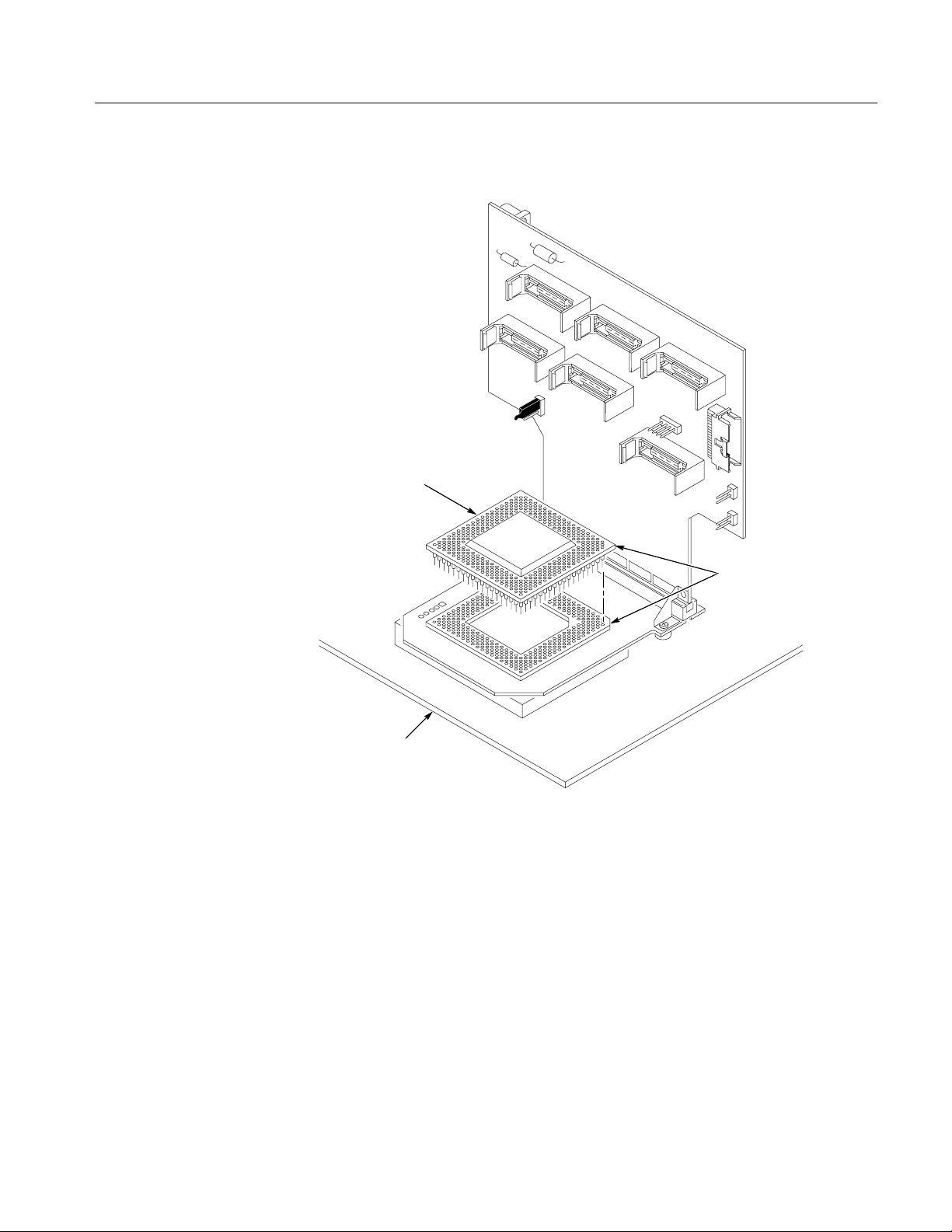
13. Insert the microprocessor into the probe adapter as shown in Figure 1–8.
PGA370
Microprocessor
Pin A3
System under test
Figure 1–8: Placing the PGA370 microprocessor into the probe adapter
14. Apply forced air cooling across the PGA370 microprocessor to keep the
microprocessor from overheating.
TMS PGA PGA370 Hardware Support
1–11
Page 28

Getting Started
Alternate Connections
APIC
Four pins on J410 are provided to connect the TMS 801 APIC bus probe adapter
to the PICCLK, PICD0 and PICD1 signals for APIC bus support. The TMS 801
APIC bus probe adapter is not included with the TMS PGA PGA370 hardware
support package. Contact a Tektronix representative for information on how to
obtain the TMS 801 APIC bus probe adapter.
Figure 1–9 shows the APIC bus signal pins for the PGA370 probe adapter.
T able 1–1: APIC information
J410
pin number
1 GND –––
2 J33 PICCLK
3 L35 PICD1
4 J35 PICD0
Microprocessor
pin number
Microprocessor
signal name
Logic board
1–12
Debug Port
J410 APIC bus pins
Figure 1–9: APIC bus pins location on the probe adapter
The PGA370 probe adapter provides J310 as a way to connect to JTAG Run
Control debugging hardware. This Run Control hardware is not included with the
TMS PGA PGA370 hardware support package. Contact your microprocessor
vendor for information on how to obtain Run Control debugging tools.
TMS PGA PGA370 Hardware Support
Page 29

Getting Started
NOTE. The debug circuitry on the Logic board is active only when the debug
probe cable is connected to J310. If the debug probe cable is disconnected from
J310, all debug data and control lines on the logic board are tristated.
Optional System Reset. The Debug port circuitry on the Interposer board does not
allow external debugging hardware to induce a system reset through the
DBRESET# signal on the Debug port connector. If you need to enable this
feature you must provide the connection to your system under test. The following
Table 1–2 lists the signals on the J510.
T able 1–2: Jumper (J510) information
Pin number Debug port signal name
1 GND
2 DBRESET#
Figure 1–10 shows the location of the DBRESET# jumper and Debug port on the
logic board of the probe adapter.
When using debugging hardware with the PGA370 probe adapter, a special
363-pin sacrificial socket must be installed in the system under test. See
Connecting the Logic Analyzer to a System Under Test on page 1–7 for further
information.
Logic board
J310 Debug port
J510
DBRESET#
Figure 1–10: Debug port and pin location on the logic board
TMS PGA PGA370 Hardware Support
1–13
Page 30

Getting Started
Test Points
Additional test points on the Interposer board at J700 allow alternate ways of
probing for information as shown on Figure 1–11. Table 1–3 lists the signals on
J700.
T able 1–3: Test point (J700) information
PGA370
J700
pin number
1 AJ33 BSEL#
2 AJ31 Reserved
3 AL31 THERMDP
4 AL29 THERMDN
5 ––– GND
Test point
microprocessor
pin
Interposer board
J700
PGA370
microprocessor
signal
Figure 1–11: Test point location on the probe adapter
Applying and Removing Power
A power supply for the PGA370 probe adapter is included with this
TMS PGA PGA370 hardware support. The power supply provides +5 volts
power to the probe adapter.
NOTE. Whenever you power off the system under test, be sure to remove power
from the probe adapter.
1–14
TMS PGA PGA370 Hardware Support
Page 31

Getting Started
To apply power to the PGA370 probe adapter and system under test, follow these
steps:
CAUTION. Failure to use the +5 V power supply provided by Tektronix can
permanently damage the probe adapter and PGA370 microprocessor. Do not
mistake another power supply that looks similar for the +5 V power supply.
1. Connect the +5 V power supply to the jack on the probe adapter. Figure 1–12
shows the location of the jack on the adapter board.
CAUTION. Failure to apply power to the probe adapter before applying power to
your system under test can permanently damage the PGA370 microprocessor and
system under test.
2. Plug the power supply for the probe adapter into an electrical outlet. When
power is present on the probe adapter, an LED lights near the power jack.
3. Power on the system under test.
Figure 1–12: Location of the power jack
Power jack
Logic board
TMS PGA PGA370 Hardware Support
1–15
Page 32

Getting Started
To remove power from the system under test and the probe adapter, follow these
steps:
CAUTION. Failure to power down your system under test before removing the
power from the probe adapter can permanently damage the PGA370 microprocessor and the system under test.
1. Power off the system under test.
2. Unplug the power supply for the probe adapter from the electrical outlet.
1–16
TMS PGA PGA370 Hardware Support
Page 33

CPU To Mictor Connections
To probe the microprocessor, you will need to make connections between the
CPU and the Mictor pins of the P6434 Mass Termination Probe. Refer to the
P6434 Mass Termination Probe manual, Tektronix part number 070-9793-XX,
for more information on mechanical specifications. Tables 1–4 through 1–11
show the CPU pin to Mictor pin connections.
Tektronix uses a counterclockwise pin assignment. Pin 1 is located at the top left,
and pin 2 is located directly below it. Pin 20 is located on the bottom right, and
pin 21 is located directly above it (see Figure1–13).
AMP uses an odd side-even side pin assignment. Pin 1 is located at the top left,
and pin 3 is located directly below it. Pin 2 is located on the top right, and pin 4
is located directly below it (see Figure1–13).
NOTE. When designing Mictor connectors into your system under test, always
follow the Tektronix pin assignment.
Getting Started
Tektronix Pinout AMP Pinout
Pin 1
Pin 19
Pin 38
Pin 20
Pin 1
Pin 37
Pin 2
Pin 38
Figure 1–13: Pin assignments for a Mictor connector (component side)
T able 1–4: Clock Channels (stored in the acquisition memory)
Clock
channel
LO_CLK:3 CLK Rising BCLK W37
LO_CLK:2 DA TA X –– ––
LO_CLK:1 DATA X –– ––
LO_CLK:0 –– X –– ––
HI_CLK:3 DATA X –– ––
HI_CLK:2 DATA X –– ––
HI_CLK:1 DATA X –– ––
HI_CLK:0 –– X –– ––
CLK,
QUAL, or DATA
Active
CLK edge
Processor
pin name
Processor
pin number
TMS PGA PGA370 Hardware Support
1–17
Page 34

Getting Started
T able 1–5: Qualifier Channels (stored in the acquisition memory)
QUAL
channel
LO_QUAL:3 –– Rising –– ––
LO_QUAL:2 –– X –– ––
LO_QUAL:1 DATA X Reserved AL21
LO_QUAL:0 DATA X Reserved G37
HI_QUAL:3 –– X –– ––
HI_QUAL:2 –– X –– ––
HI_QUAL:1 DATA X Reserved AN21
HI_QUAL:0 DATA X Reserved F10
QUAL, or DATA
Active
CLK edge
Processor
pin name
Processor
pin number
NOTE. Dashes –– indicates: the CLK or QUAL channel is not used, the channel
is not supported by the support software, or the channel is not connected to the
microprocessor.
CLK and QUAL channels designated as DATA are logged in on the master strobe
defined by the support software.
T able 1–6: CPU to Mictor connections for Mictor C pins (high)
1–18
Tektronix
Mictor A
pin number
4 7 C3:7 FLUSH# AE37
8 15 C3:3 Reserved C33
12 23 C2:7 Reserved A31
16 31 C2:3
5 9 C3:6 INIT# AG33
9 17 C3:2 Reserved A33
13 25 C2:6 Reserved A29
17 33 C2:2
6 11 C3:5 PRDY# A35
10 19 C3:1 Reserved C31
14 27 C2:5 Reserved C29
18 35 C2:1
7 13 C3:4 Not Specified Not Specified
11 21 C3:0 Not Specified Not Specified
AMP
Mictor A
pin number
LA channel
1
1
1
Processor
pin name
RESET# X4
Reserved AK16
BREQ0# AN29
Processor
pin number
TMS PGA PGA370 Hardware Support
Page 35

T able 1–6: CPU to Mictor connections for Mictor C pins (high) (cont.)
Getting Started
Tektronix
Mictor A
pin number
15 29 C2:4 Not Specified Not Specified
19 37 C2:0
35 8 C1:7 Derived Derived
31 16 C1:3 Derived Derived
27 24 C0:7 Derived Derived
23 32 C0:3 Not Specified Not Specified
34 10 C1:6 Derived Derived
30 18 C1:2 Derived Derived
26 26 C0:6 Derived Derived
22 34 C0:2 Derived Derived
33 12 C1:5 SLP# AH30
29 20 C1:1 Derived Derived
25 28 C0:5 Derived Derived
21 36 C0:1 Derived Derived
32 14 C1:4 Derived Derived
28 22 C1:0 Derived Derived
24 30 C0:4 Derived Derived
20 38 C0:0 PWRGOOD AK26
AMP
Mictor A
pin number
LA channel
1
Processor
pin name
Derived Derived
Processor
pin number
T able 1–7: CPU to Mictor connections for Mictor A pins (high)
Tektronix
Mictor A
pin number
4 7 A3:7 D62# E25
5 9 A3:6 D61# A27
6 11 A3:5 D55# C19
7 13 A3:4 D60# A25
8 15 A3:3 D53# A23
9 17 A3:2 D57# A19
10 19 A3:1 D46# A21
11 21 A3:0 D49# C13
TMS PGA PGA370 Hardware Support
AMP
Mictor A
pin number
LA channel
Processor
pin name
Processor
pin number
1–19
Page 36

Getting Started
T able 1–7: CPU to Mictor connections for Mictor A pins (high) (cont.)
Tektronix
Mictor A
pin number
12 23 A2:7 D51# A13
13 25 A2:6 D42# D12
14 27 A2:5 D45# C1 1
15 29 A2:4 D39# D10
16 31 A2:3 D40# C15
17 33 A2:2 D34# C7
18 35 A2:1 D38# D8
19 37 A2:0 D32# F6
35 8 A1:7 D58# C23
34 10 A1:6 D63# F16
33 12 A1:5 D56# C27
32 14 A1:4 D50# C25
31 16 A1:3 D54# C21
30 18 A1:2 D59# C17
29 20 A1:1 D48# A17
28 22 A1:0 D52# D16
27 24 A0:7 D41# D14
26 26 A0:6 D47# A15
25 28 A0:5 D44# A11
24 30 A0:4 D36# C9
23 32 A0:3 D43# A7
22 34 A0:2 D37# A9
21 36 A0:1 D33# C1
20 38 A0:0 D35# B2
AMP
Mictor A
pin number
LA channel
Processor
pin name
Processor
pin number
1–20
T able 1–8: CPU to Mictor connections for Mictor D pins (high)
Tektronix
Mictor A
pin number
4 7 D3:7 D28# A5
5 9 D3:6 D29# A3
6 11 D3:5 D26# E1
7 13 D3:4 D25# E3
8 15 D3:3 D22# F8
AMP
Mictor A
pin number
LA channel
Processor
pin name
TMS PGA PGA370 Hardware Support
Processor
pin number
Page 37

T able 1–8: CPU to Mictor connections for Mictor D pins (high) (cont.)
Getting Started
Tektronix
Mictor A
pin number
9 17 D3:2 D19# H6
10 19 D3:1 D18# P4
11 21 D3:0 D20# L3
12 23 D2:7 D17# R4
13 25 D2:6 D15# U3
14 27 D2:5 D12# Q1
15 29 D2:4 D7# J1
16 31 D2:3 D6# T6
17 33 D2:2 D5# S3
18 35 D2:1 D3# M6
19 37 D2:0 D1# T4
35 8 D1:7 D31# C5
34 10 D1:6 D30# J3
33 12 D1:5 D27# F12
32 14 D1:4 D24# K6
31 16 D1:3 D23# G3
30 18 D1:2 D21# G1
29 20 D1:1 D16# H4
28 22 D1:0 D13# L1
27 24 D0:7 D11# M4
26 26 D0:6 D10# Q3
25 28 D0:5 D14# N3
24 30 D0:4 D9# P6
23 32 D0:3 D8# S1
22 34 D0:2 D4# U1
21 36 D0:1 D2# N1
20 38 D0:0 D0# W1
AMP
Mictor A
pin number
LA channel
Processor
pin name
Processor
pin number
T able 1–9: CPU to Mictor connections for Mictor C pins (Low)
Tektronix
Mictor A
pin number
4 7 C3:7 Reserved AN11
8 15 C3:3 Reserved AN23
TMS PGA PGA370 Hardware Support
AMP
Mictor A
pin number
LA channel
Processor
pin name
Processor
pin number
1–21
Page 38

Getting Started
T able 1–9: CPU to Mictor connections for Mictor C pins (Low) (cont.)
Tektronix
Mictor A
pin number
AMP
Mictor A
pin number
LA channel
Processor
pin name
Processor
pin number
12 23 C2:7 Reserved AN13
16 31 C2:3
1
Reserved AL11
5 9 C3:6 BNR# AH14
9 17 C3:2 LOCK# AK20
13 25 C2:6 DBSY# AL27
17 33 C2:2
1
Reserved AK24
6 11 C3:5 BPRI# AN17
10 19 C3:1 DRDY# AN27
14 27 C2:5 RS2# AK28
18 35 C2:1
1
ADS# AN31
7 13 C3:4 Reserved AL13
11 21 C3:0 Reserved AN15
15 29 C2:4 Not Specified Not Specified
19 37 C2:0
1
Not Specified Not Specified
35 8 C1:7 Reserved AF4
31 16 C1:3 Reserved W3
27 24 C0:7 Reserved AC1
23 32 C0:3 Reserved X6
34 10 C1:6 RS1# AH22
30 18 C1:2 RS0# AH26
26 26 C0:6 DEFER AN19
22 34 C0:2 HITM# AL23
33 12 C1:5 Reserved V4
29 20 C1:1 REQ4# AL17
25 28 C0:5 HIT# AL25
21 36 C0:1 TRDY# AN25
32 14 C1:4 REQ3# AL19
28 22 C1:0 REQ2# AH18
24 30 C0:4 REQ1# AH16
20 38 C0:0 REQ0# AK18
1
Possible qualifier line
2
Signal is active low
1–22
TMS PGA PGA370 Hardware Support
Page 39

T able 1–10: CPU to Mictor connections for Mictor A pins (Low)
Getting Started
Tektronix
Mictor A
pin number
4 7 A3:7 A31# AD4
5 9 A3:6 A30# AA3
6 11 A3:5 A29# Z4
7 13 A3:4 A28# AK6
8 15 A3:3 A27# AA1
9 17 A3:2 A26# Y3
10 19 A3:1 A25# AF6
11 21 A3:0 A24# AB4
12 23 A2:7 A23# AB6
13 25 A2:6 A22# AE3
14 27 A2:5 A21# AJ1
15 29 A2:4 A20# AC3
16 31 A2:3 A19# AG3
17 33 A2:2 A18# Z6
18 35 A2:1 A17# AE1
19 37 A2:0 A16# AN7
35 8 A1:7 A15# AL5
34 10 A1:6 A14# AK14
33 12 A1:5 A13# AL7
32 14 A1:4 A12# AN5
31 16 A1:3 A11# AK10
30 18 A1:2 A10# AH6
29 20 A1:1 A9# AL9
28 22 A1:0 A8# AH10
27 24 A0:7 A7# AL15
26 26 A0:6 A6# AN9
25 28 A0:5 A5# AH8
24 30 A0:4 A4# AH12
23 32 A0:3 Derived Derived
22 34 A0:2 Derived Derived
21 36 A0:1 Derived Derived
20 38 A0:0 Derived Derived
AMP
Mictor A
pin number
LA channel
Processor
pin name
Processor
pin number
TMS PGA PGA370 Hardware Support
1–23
Page 40

Getting Started
T able 1–11: CPU to Mictor connections for Mictor D pins (Low)
Tektronix
Mictor A
pin number
4 7 D3:7 Derived Derived
5 9 D3:6 Derived Derived
6 11 D3:5 Derived Derived
7 13 D3:4 Derived Derived
8 15 D3:3 TDO AN37
9 17 D3:2 THERMTRIP# AH28
10 19 D3:1 LINT0/INTR M36
11 21 D3:0 PICD0 J35
12 23 D2:7 PREQ# J37
13 25 D2:6 BPM0# C35
14 27 D2:5 BCLK W37
15 29 D2:4 STPCLK# AG35
16 31 D2:3 TCK AL33
17 33 D2:2 TDI AM35
18 35 D2:1 A20M# AE33
19 37 D2:0 BP3# E37
35 8 D1:7 IERR# AE35
34 10 D1:6 FERR# AC35
33 12 D1:5 IGNNE# AG37
32 14 D1:4 TMS AK32
31 16 D1:3 TRST# AN33
30 18 D1:2 LINT1/NM1 L37
29 20 D1:1 PICCLK# J33
28 22 D1:0 BP2# G33
27 24 D0:7 PICD1 L35
26 26 D0:6 BPM1# E35
25 28 D0:5 Reserved Y1
24 30 D0:4 SMI# AJ35
23 32 D0:3 Reserved B36
22 34 D0:2 Reserved E31
21 36 D0:1 Reserved E29
20 38 D0:0 Not Specified Not Specified
AMP
Mictor A
pin number
LA channel
Processor
signal name
Processor
signal name
1–24
TMS PGA PGA370 Hardware Support
Page 41

Specifications
Page 42

Page 43

Specifications
Circuit Description
This chapter contains information regarding the specifications of the
TMS PGA PGA370 microprocessor hardware support.
The following is a description of Signal Probing, Bus Tracking Logic, and Debug
circuitry.
Debug Port
The PGA370 probe adapter provides a connection point for a Debug Port. In
addition to the standard debug port, the probe adapter contains circuitry to
terminate the debug control and data signals to their appropriate voltage levels.
The debug circuitry on the probe adapter supports both 1.5 V CMOS I/O and
2.5V CMOS I/O. The debug circuitry on the probe adapter uses the VCC_CMOS
signal on the microprocessor to detect the CMOS I/O voltage level.
When using the debug port on the probe adapter, a 363-pin sacrificial socket
must be installed on the system under test to isolate the debug signals between
the system under test and the microprocessor. Isolating the debug signals allows
the probe adapter to control the debug signals on the local CPU.
The debug circuitry on the probe adapter can only control the debug signals when
an debug probe cable is plugged into the debug port on the logic board. When the
cable is removed, all debug data and control lines are tristated.
TMS PGA PGA370 Hardware Support
2–1
Page 44
Specifications
Probe Adapter Loading Diagrams
Figures 2–1 through 2–5 are provided for loading reference.
Connect to PPGA CPU
Interposer
PGA370 Socket
Sacrificial
PGA370 Socket
Connect to PGA 370
socket on system
under test
87 W
0.06 nS
151 W 87 W 87 W
0.5 pF
0.55 nS 0.58 nS
Figure 2–1: PGA370 signals without active loads
Connect to PPGA CPU
Interposer
PGA370
Sacrificial
PGA370
Connect to PGA 370 socket
on system under test
87 W
0.06 nS
100 W
0.5 pF
0.40 nS
Figure 2–2: PGA370 signals with active loads
87 W
Mated 190 - Pin
Mictor Model
Mated 190 - Pin
Mictor Model
87 W
0.15 nS
P6434
Probe
6.5 pF
87 W
P6434
Probe
0.60 nS
2–2
Connect to PPGA CPU
Interposer
PGA370
Sacrificial
PGA370
Connect to PGA 370 socket
on system under test
87 W 182 W
0.08 nS
Figure 2–3: PGA370 BCLK
0.5 pF
87 W
0.02 nS
332 W
2.6 pF
TMS PGA PGA370 Hardware Support
Page 45

Interposer
PGA370 Socket
CPU
1.0 nH
Sacrificial
PGA370 Socket
CPU
1.5 nH
Specifications
Mated 190 - Pin
Mictor Model
Input Output
10 mW
3.2 nH
1.3 nH
System under test
0.5
pF
System under test
0.7
pF
Figure 2–4: Detail of PGA370 sockets and 190-pin mictor connector.
0.5
pF
TMS PGA PGA370 Hardware Support
2–3
Page 46

Specifications
Table 2–1 shows the values you can use to calculate characteristics of the Lossy
delay lines shown in Figure 2–5, which is the equivalent circuit of the P6434
probe.
T able 2–1: Lossy delay line values
Characteristic V alue
C (capacitance) 1.58 pF per inch
L (inductance) 8.9 nH per inch
R (resistance)
Z0 (impedance)
Input
1.6 nH
0.005
0.7 pF
W
1.6 nH
0.005
W
1.1 pF
Figure 2–5: Equivalent circuit for the P6434 probe
.067 W per inch
75 W
0.23 pF
20 KW
LOSS Y
Length = 58 inches
75
W
+2.2 V
2–4
TMS PGA PGA370 Hardware Support
Page 47

Specification Tables
Specifications
These specifications are for a probe adapter connected between a compatible
Tektronix logic analyzer and a system under test. Signal voltage swing in your
system under test must be at least 200 mV around the GTL+ reference voltage.
Table 2–2 lists the electrical requirements of the system under test. Table 2–3
lists the electrical requirements for the power supply that provides power to the
PGA370 probe adapter. Table 2–4 lists the environmental specifications.
Table 2–5 lists the BCLK timing restrictions and electrical specifications.
T able 2–2: Electrical specifications for the system under test
Characteristics Requirements
System under test DC power requirements
Voltage, VCC_1.5 V
Current, VCC_1.5 V I maximum 35 mA, I typical 1.8 mA
Voltage, VREF6
Current, VREF6 I maximum <1 mA, I typical <1 mA
Voltage, VCC_CMOS (1.5 V)
Current, VCC_CMOS (1.5 V)
Voltage, VCC_CMOS (2.5 V)
Current, VCC_CMOS (2.5 V)
System under test clock rate Maximum 100 MHz
System under test tested clock rate Maximum 100 MHz
Minimum setup time required, all signals 2.8 ns
Minimum hold time required, all signals 0.2 ns
Measured typical SUT signal loading AC load DC load
All signals with active loads (except
BCLK): INIT#, BREQ0#, REQ4#,
RESET#, ADS#, RS0#, RS1#, RS2#,
HIT#, HITM#, DRDY#, BNR#, A3#, A8#
– A15#,
1
1
1
1
1.5 V "9 %
1.0 V "2 %
1.5 V "9 %
I maximum 20 mA, I typical 0.9 mA
2.5 V "5 %
I maximum 35 mA, I typical 1.4 mA
Specification
8 pF 74GTL16622 in parallel
with 20 kW
BCLK 2.6 pF AD8009
Signals without active loads 2.5 pF
1
TMS PGA PGA370 Hardware Support
20 kW
The VCC_CMOS supply voltage can be either 1.5. V or 2.5 V depending on the CMOS
I/O voltage level of the target microprocessor.
2–5
Page 48

Specifications
T able 2–3: Electrical specifications for the AC adapter
Characteristic Description
Input Voltage rating 90 – 265 V
Input Frequency Rating 47 – 63 Hz
Output Voltage Rating 5 V
Output Current Rating 5 V
Output Power Rating 25 W
T able 2–4: Environmental specifications
Characteristic
1
Description
Temperature
Maximum operating +50° C (+122° F)
2
Minimum operating 0° C (+32° F)
Nonoperating –55° C to +75° C (–67° to +167° F)
Humidity 10 to 95% relative humidity
Altitude
Operating 4.5 km (15,000 ft) maximum
Nonoperating 15 km (50,000 ft) maximum
Electrostatic immunity The probe adapter is static sensitive
1
Designed to meet Tektronix standard 062-2847-00 class 5.
2
Not to exceed microprocessor thermal considerations. Forced air cooling might be
required across the CPU.
T able 2–5: BCLK timing and electrical specifications
Characteristics
Vin (lo) 0.5 V
Vin (hi) 2.0 V
Duty Cycle 25 75 %
t
lh
t
hl
Minimum Maximum Units Notes
1.25 ns Monotonically increasing
1.25 ns Monotonically decreasing
2–6
TMS PGA PGA370 Hardware Support
Page 49

Specifications
Dimensions
Logic board
Interposer board
97.79 mm
(3.850 in)
Figure 2–6 shows the dimensions of the PGA370 probe adapter. The figure also
shows the minimum vertical clearance of the high-density probe cable.
139.06 mm
(5.475 in)
15.75 mm
(.620 in)
53.34 mm
(2.100 in)
4.32 mm
(.170 in)
133.35 mm
(5.250 in)
28.32 mm
(1.115 in)
Sacrificial
socket
4.39 mm
(.170 in)
93.98 mm
(3.700 in)
Figure 2–6: Dimensions of the PGA370 probe adapter
34.29 mm
(1.350 in)
10.16 mm
(.400 in)
13.58 mm
(.535 in)
76.20 mm
(3.00 in)
23.49 mm
(.925 in)
9.78 mm
(.385 in)
72.40 mm
(2.850 in)
TMS PGA PGA370 Hardware Support
2–7
Page 50

Specifications
2–8
TMS PGA PGA370 Hardware Support
Page 51

WARNING
The following servicing instructions are for use only by qualified personnel. To
avoid injury, do not perform any servicing other than that stated in the operating
instructions unless you are qualified to do so. Refer to all safety summaries before
performing any service.
Page 52

Page 53

Maintenance
Page 54

Page 55

Maintenance
Replacing The Fuse
This section contains information on replacing the PGA370 probe-adapter fuse.
If the fuse on the probe adapter opens (burns out), you can replace it with a 5 A,
125 V fuse. Figures 3–1 illustrates the location of the fuse on the PGA370 probe
adapter. See the Replaceable Mechanical Parts chapter for part descriptions.
F200 Fuse
Figure 3–1: Fuse location on the PGA370 probe adapter
TMS PGA PGA370 Hardware Support
3–1
Page 56

Maintence
3–2
TMS PGA PGA370 Hardware Support
Page 57

Replaceable Mechanical Parts
Page 58

Page 59

Replaceable Parts List
This chapter contains a list of the replaceable components for the
TMS PGA PGA370 Hardware Support product.
Parts Ordering Information
Replacement parts are available through your local Tektronix field office or
representative.
Changes to Tektronix products are sometimes made to accommodate improved
components as they become available and to give you the benefit of the latest
improvements. Therefore, when ordering parts, it is important to include the
following information in your order:
H Part number
H Instrument type or model number
H Instrument serial number
H Instrument modification number, if applicable
If you order a part that has been replaced with a different or improved part, your
local Tektronix field office or representative will contact you concerning any
change in part number.
Change information, if any, is located at the rear of this manual.
Using the Replaceable Parts List
The tabular information in the Replaceable Parts List is arranged for quick
retrieval. Understanding the structure and features of the list will help you find
all of the information you need for ordering replacement parts. The following
table describes the content of each column in the parts list.
TMS PGA PGA370 Hardware Support
4–1
Page 60

Replaceable Parts List
Parts list column descriptions
Column Column name Description
1 Figure & index number Items in this section are referenced by figure and index numbers to the exploded view illustrations
that follow.
2 T ektronix part number Use this part number when ordering replacement parts from Tektronix.
3 and 4 Serial number Column three indicates the serial number at which the part was first effective. Column four
indicates the serial number at which the part was discontinued. No entries indicates the part is
good for all serial numbers.
5 Qty This indicates the quantity of parts used.
6 Name & description An item name is separated from the description by a colon (:). Because of space limitations, an
item name may sometimes appear as incomplete. Use the U.S. Federal Catalog handbook H6-1
for further item name identification.
7 Mfr. code This indicates the code of the actual manufacturer of the part.
8 Mfr. part number This indicates the actual manufacturer’s or vendor’s part number.
Abbreviations
Chassis Parts
Mfr. Code to Manufacturer
Cross Index
Abbreviations conform to American National Standard ANSI Y1.1–1972.
Chassis-mounted parts and cable assemblies are located at the end of the
Replaceable Electrical Parts List.
The table titled Manufacturers Cross Index shows codes, names, and addresses of
manufacturers or vendors of components listed in the parts list.
4–2
TMS PGA PGA370 Hardware Support
Page 61

Replaceable Parts List
Manufacturers cross index
Mfr.
code
00779 AMP INC. CUSTOMER SERVICE DEPT
14310 AULT INC 7300 BOONE AVE NORTH
1AW87 LEWIS SCREW CO. 4300 SOUTH RACINE AVENUE CHICAGO, IL 60609
26742 METHODE ELECTRONICS INC BACKPLAIN DIVISION
5Y400 TRIAX METAL PRODUCTS INC 1880 SW MERLO DRIVE BEAVERTON, OR 97006
60381 PRECISION INTERCONNECT CORP. 16640 SW 72ND AVE PORTLAND, OR 97224
61857 SAN–O INDUSTRIAL CORP 91–3 COLIN DRIVE HOLBROOK, NY 11741
63058 BERG ELECTRONICS INC. MCKENZIE SOCKET DIV
80009 TEKTRONIX INC 14150 SW KARL BRAUN DR
82389 SWITCHCRAFT DIV OF RAYTHEON
S3109 FELLER U.S. CORPORATION 72 VERONICA AVE
TK1373 PATELEC–CEM 10156 TORINO
TK2541 AMERICOR ELECTRONICS LTD UNIT–H
TK2548 XEROX CORPORATION 14181 SW MILLIKAN WAY BEA VER T ON, OR 97005
Manufacturer Address City , state, zip code
PO BOX 3608
BROOKLINE PARK
7444 WEST WILSON AVE
910 PAGE AVE
PO BOX 500
5555 N. ELSTON AVENUE
UNIT #4
VAICENTALLO
62/456
2682 W COYLE AVE
HARRISBURG, PA 17105–3608
MINNEAPOLIS, MN 55428
CHICAGO, IL 60656–4548
FREMONT , CA 94538–7340
BEAVERT ON, OR 97077–0001
CHICAGO, IL 60630–1314
SOMERSET, NJ 08873
ITALY,
ELK GROVE VILLAGE, IL 60007
TMS PGA PGA370 Hardware Support
4–3
Page 62

Replaceable Parts List
Replaceable parts list
Fig. &
index
number
5–1–0 010–0626–00 1 ADAPTER,PROBE:100MHZ SOCKETED 370 PIN
–1 671–4707–00 1 CIRCUIT BD ASSY:370 PIN PPGA,SOCKETED LOGIC
–2 131–6610–00 1 JACK,POWER DC:PCB,MALE,RTANG,2MM PIN
–3 131–1857–00 1 CONN, HDR: PCB, MALE, STR, 1 X 36, 0.1 CTR, 0.230 MLG X
–4 131–4850–00 1 CONN,HDR:PCB,MALE,RTANG,2 X 15,0.05 X 0.1 CTR,0.35 H X
–5 131–4917–00 2 CONN, HDR: PCB, MALE, STR,1 X 2, 0.1 CTR, 0.235 MLG X
–6 211–0022–00 2 SCREWS,MACHINE 2–56 X 0.188,PNH,STL CD PL,POZ 05276 6151
–7 136–1340–00 1 SOCKET,PGA:PCB,CUSTOM INTERSTITIAL PGA,FEMALE,370
–8 136–1338–00 1 SOCKET,PGA:PCB,CUSTOM INTERSTITIAL PGA,FEMALE,370
–9 671–4706–00 1 CIRCUIT BD ASSY370 PIN,PPGA,SOCKETED,BASE
–10 407–4677–00 2 BRACKET BOARD MOUNT ,0.036 CRS 5Y400 407–4677–00
–11 131–4356–00 1 CONN,SHUNT :SHUNT/SHORTING,FEMALE,1 X 2,0.1 CTR,0.63
–12 131–4530–00 1 CONN,HDR:PCB,MALE,STR,1 X 3,0.1 CTR,0.230 MLG X 0.120
–13 105–1089–00 6 LATCH ASSY:LATCH HOUSING ASSY,VERTICAL MOUNT,0.48
–14 131–6134–01 6 CONN,PLUG:SMD,MICTOR,PCB,FEMALE,STR,38 POS,0.025
–15 159–0059–00 1 FUSE,WIRE LEAD:5A,125V 61857 SPI–5A
Tektronix part
number
071–0475–01 1 MANUAL,TECH:INSTRUCTIONS,PPGA HARDWARE
161–0104–00 1 CA ASSY,PWR:3,18 AWG,98 L,250V/10AMP,98
119–5061–01 1 POWER SUPPLY :25W,5V 5A,CONCENTRIC
––––––––––
161–0104–05 1 CA ASSY,PWR:3,1.0MM SQ,250V/10A,2.5
Serial no.
effective
Serial no.
discont’d
Qty Name & description
PPGA;TMS112 OPT 03
BD,TMS112 OPT 03
DIA,BRASS,SILVER PLATE,5A,
0.100 TAIL, GOLD
0.10 TAIL,CTR PLZ,LATCHING,30 GOL
0.110 TAIL, 30 GOLD, TUBE, HIGH TEMP
POS,WITH 7 PINS REMOVED,STR,OPEN CENTER,0
POS,STR,OPEN CENTER,0.180 L CONTACTS,30 G
BD,;TMS112 OPT 03
H,BLK,W/HANDLE,JUMPER,30 GOLD,
TAIL,30 GOLD,BD RETENTION,
H X 1.24 L,W/PCB SINGLE CLIP,P6434
CTR,0.245 H,GOLD,TLA7QS
STANDARD ACCESSORIES
SUPPORT ,TMSPGA,DP
INCH,RT ANG,IEC320,RCPT X STR,NEMA 15–5P,W/CORD
GRIP,
2MM,90–265V,47–63 HZ IEC,15X8.6X5 CM, UL,CSA,
TUV,IEC,SELF
OPTIONAL ACCESSORIES
Mfr.
code
80009 010–0626–00
80009 671–4707–00
82389 RAPC722TB
22526 65507–136
00779 104069–5
00779 104350–1
63058 PZA–363H–120B–3
63058 PGA–144H101B1–1
80009 671–4706–00
26742 9618–302–50
00779 104344–1
60381 105–1089–00
00779 767054–1
TK2548 071–0475–01
S3109 ORDER BY
14310 SW108KA0002F01
Mfr. part number
7BL–F
302–R
DESCRIPTION
* 6 P6434 MASS TERMINATION PROBE, Opt 21 * 80009 ORDER BY
DESCRIPTION
METER,RTANG,IEC320,RCPT,AUSTRALIA,SAFTEY
CONTROLLED,
TK1373 161–0104–05
4–4
TMS PGA PGA370 Hardware Support
Page 63

Replaceable parts list (cont.)
Fig. &
index
number
Tektronix part
number
161–0104–06 1 CA ASSY,PWR:3,1.0MM SQ,250V/10A,2.5
161–0104–07 1 CA ASSY,PWR:3,1.0MM SQ,240V/10A,2.5
161–0167–00 1 CA ASSY,PWR:3,0.75MM SQ,250V/10A,2.5
Serial no.
effective
* Check the P6434 manual for detailed replaceable part number information.
Serial no.
discont’d
Name & descriptionQty
METER,RTANG,IEC320,RCPT,EUROPEAN,SAFTEY
CONTROLLED,
METER,RTANG,IEC320,RCPT X 13A,FUSED,UK PLUG,(13A
FUSE),UK PLUG,(13A FUSE),UNITED KINGDOM,SAFTEY
CONTROL
METER,RTANG,IEC320,RCPT,SWISS,NO CORD
GRIP,SAFTEY CONTR
Replaceable Parts List
Mfr.
code
TK1373 ORDER BY
TK2541 ORDER BY
S3109 ORDER BY
Mfr. part number
DESCRIPTION
DESCRIPTION
DESCRIPTION
TMS PGA PGA370 Hardware Support
4–5
Page 64

Replaceable Parts List
13
14
1
15
12
11
6
10
2
3
4
5
6
9
8
Figure 4–1: PGA370 probe adapter exploded view
7
4–6
TMS PGA PGA370 Hardware Support
Page 65

Index
Page 66

Page 67

Index
Numbers
40 MHz system under test, 1–6
A
about this manual set, vii
AC adapter, 2–6
acquiring data, below 40 MHz, 1–6
Alternate Connections
APIC bus support, 1–12
Debug Port, 1–12
T est Points, 1–14
APIC, 1–12
APIC bus support, logic analyzer configuration, 1–2
application, logic analyzer configuration, 1–2
Assembling Probe Adapter, 1–4
B
BCLK, 1–2
C
clock rate, 1–2
connections
CPU to Mictor, 1–17
probe adapter to SUT, 1–7
cooling requirements, 1–2
CPU to Mictor connections, 1–17
clock rate, 2–5
hold time, 2–5
power requirements, 2–5
setup time, 2–5
signal loading, 2–5
tested clock rate, 2–5
environmental specifications, 2–6
altitude, 2–6
electrostatic immunity, 2–6
humidity , 2–6
temperature, 2–6
F
fuse, replacing, 3–1
H
HI module, definition, vii
I
installing hardware. See Alternate Connections
ITP bus support, logic analyzer configuration, 1–2
J
jumpers
MFG_TEST, 1–6
timing, 1–6
D
Debug Port. See Alternate Connections
definitions
HI module, vii
information on basic operations, vii
LO module, vii
module, vii
dimensions, probe adapter, PGA370, 2–7
disassembler, logic analyzer configuration, 1–2
E
electrical specifications, 2–1, 2–5
AC adapter, 2–6
BCKL timing, 2–6
TMS PGA PGA370 Hardware Support
L
LO module, definition, vii
loading, 2–5
logic analyzer
configuration for disassembler, 1–2
configuration for the application, 1–2
M
manual
conventions, vii
how to use the set, vii
MFG_TEST pins, 1–6
Mictor to CPU connections, 1–17
Index–1
Page 68

Index
module, definition, vii
P
P6434 probes, labeling, 1–3
power, for the probe adapter
applying, 1–14
removing, 1–15
power adapter, 1–14
power jack, 1–15
probe adapter
clearance, dimensions, PGA370, 2–7
configuring, 1–6
Connecting the logic Analyzer, 1–7
hardware description, 1–1
jumper positions, 1–6
R
replacing the fuse, 3–1
requirements
cooling, 1–2
forced air cooling, 1–2
Signal Supported, 1–3
System under T est, 1–2
restrictions, 1–2
BCLK, 1–2
S
service information, 3–1
signal loading, 2–5
Signal Supported, 1–3
signals, active low sign, vii
sockets, 370 pin or 363 pin, 1–8
specifications, 2–1
electrical, 2–1, 2–5
environmental, 2–6
mechanical (dimensions), PGA370, 2–7
System Under T est power, 1–2
T
terminology, vii
T est Points. See Alternate Connections
TIMING/NORMAL jumper, 1–6
Index–2
TMS PGA PGA370 Hardware Support
 Loading...