

Page 1

Instruction Manual
TMS809 AGP 3.0 Bus Support
071-1084-00
Warning
The servicing instructions are for use by qualified
personnel only. To avoid personal injury, do not
perform any servicing unless you are qualified to
do so. Refer to all safety summaries prior to
performing service.
www.tektronix.com
Page 2

Copyright © Tektronix, Inc. All rights reserved. Licensed software products are owned by Tektronix or its suppliers and
are protected by United States copyright laws and international treaty provisions.
Use, duplication, or disclosure by the Government is subject to restrictions as set forth in subparagraph (c)(1)(i i) of the
Rights in Technical Data and Computer Software clause at DFARS 252.227-7013, or subparagraphs (c)(1) and (2) of the
Commercial Computer Software -- Restricted Rights clause at FAR 52.227-19, as applicable.
Tektronix products are covered by U.S. and foreign patents, issued and pending. Information in this publication supercedes
that in all previously published material. Specifications and price change privileges reserved.
Tektronix, Inc., P.O. Box 500, Beaverton, OR 97077
TEKTRONIX and TEK are registered tradem arks of Tektronix, Inc.
Page 3

SOFTWARE WARRANTY
Tektronix warrants that the media on which thi s software product is furnished and the encoding of the programs on
the media will be free from defects in materials and workmanship for a period of three (3) months from the dat e of
shipment. If a medium or encoding proves defective during the warranty period, Tektronix will provide a
replacement in exchange for the defective medium. Except as to the media on which this software product is
furnished, this software product is provided “as is” without warranty of any kind, either express or implied.
Tektronix does not warrant that the functions contained in this software product will meet Customer’s
requirements or that the operation of the programs will be uninte rrupted or error-free.
In order to obtain service under this warranty, Customer must notify Tektronix of the defect before the expiration
of the warranty period. If Tektronix is unable to provide a replacement that is free from defects in materials and
workmanship within a reasonable time thereafter, Customer may terminate the license for this software product
and return this software product and any associated materials for credit or refund.
THIS W ARRANTY IS GIVEN BY TEKTRONIX IN LIEU OF ANY OTHER WARRANTIES, EXPRESS
OR IMPLIED. TEKTRONIX AND ITS VENDORS DISCLAIM ANY IMPLIED WARRANTIES OF
MERCHANTABILITY OR FITNESS FOR A PARTICULAR PURPOSE. TEKTRONIX’
RESPONSIBILITY TO REPLACE DEFECTIVE MEDIA OR REFUND CUSTOMER’S PAYMENT IS
THE SOLE AND EXCLUSIVE REMEDY PROVIDED TO THE CUSTOMER FOR BREACH OF THIS
WARRANTY. TEKTRONIX AND ITS VENDORS WILL NOT BE LIABLE FOR ANY INDIRECT,
SPECIAL, INCIDENTAL, OR CONSEQUENTIAL DAMAGES IRRESPECTIVE OF WHETHER
TEKTRONIX OR THE VENDOR HAS ADVANCE NOTICE OF THE POSSIBILITY OF SUCH
DAMAGES.
Page 4

HARDWARE WARRANTY
Tektronix warrants that the products that it m anufactures and sells will be free from defects in materials and
workmanship for a period of one (1) year from the date of shipment. If a product proves defect ive during this
warranty period, Tektronix, at its option, ei ther will repa ir the defec tive product without charge for parts and labor,
or will provide a replacement in exchange for the defective product.
In order to obtain service under this warranty, Customer must notify Tektronix of the defect before the expiration
of the warranty period and make suitable arrangements for the performance of service. Customer shall be
responsible for packaging and shipping the defective product to the service center designated by Tektronix, with
shipping charges prepaid. Tektronix shall pay for the return of the product to Customer if the shipment i s to a
location within the country in which the Tektronix service center is located. Customer shall be responsible for
paying all shipping charges, duties, taxes, and any other charges for products returned to any other locations.
This warranty shall not apply to any defe ct, fail ure or damage caused by improper use or improper or inadequate
maintenance and care. Tektronix shall not be obligated to furnish service under this warranty a) to repair damage
resulting from attempts by personnel other than Tektronix representatives to install, repair or service the product;
b) to repair damage resulting from improper use or connection to incompatible equipment; c) to repair any
damage or malfunction caused by the use of non-Tektronix supplies; or d) to service a product that has been
modified or integrated with other products when the effect of such modification or integration increases the time
or difficulty of servicing the product.
THIS W ARRANTY IS GIVEN BY TEKTRONIX IN LIEU OF ANY OTHER WARRANTIES, EXPRESS
OR IMPLIED. TEKTRONIX AND ITS VENDORS DISCLAIM ANY IMPLIED WARRANTIES OF
MERCHANTABILITY OR FITNESS FOR A PARTICULAR PURPOSE. TEKTRONIX’
RESPONSIBILITY TO REPAIR OR REPLACE DEFECTIVE PRODUCTS IS THE SOLE AND
EXCLUSIVE REMEDY PROVIDED TO THE CUSTOMER FOR BREACH OF THIS WARRANTY.
TEKTRONIX AND ITS VENDORS WILL NOT BE LIABLE FOR ANY INDIRECT, SPECIAL,
INCIDENTAL, OR CONSEQUENTIAL DAMAGES IRRESPECTIVE OF WHETHER TEKTRONIX OR
THE VENDOR HAS ADVANCE NOTICE OF THE POSSIBILITY OF SUCH DAMAGES.
Page 5

Table of Contents
Getting Started
Operating Basics
General Safety Summary vii..........................................
Service Safety Summary ix..........................................
Manual Conventions xi..............................................
Contacting Tektronix xii.............................................
Probe Adapter Description 1--1.........................................
Logic Analyzer Software Compatibility 1--1..............................
Logic Analyzer Configuration 1--2......................................
Probe Adapter Review 1--4............................................
Components and Standard Accessories 1--5...............................
Configuring the Probe Adapter 1--6....................................
Connecting the Logic Analyzer to a Target System 1--7.....................
Verifying Probe Operation 1--23........................................
Replacing the Pogo Pin Assembly (Backside Board) 1--25....................
Storage 1--26........................................................
Care and Maintenance 1--27............................................
Shipping the Probe Adapter 1--28.......................................
Reference
Specifications
Maintenance
Installing the Software 2-- 1............................................
Support Package Setups 2--2...........................................
Channel Group Definitions 2--2.........................................
Symbol Tables 2--2..................................................
Acquiring and Viewing Disassembled Data 2--3............................
Viewing an Example of Disassembled Data 2--7...........................
Symbol Tables 3-- 1............................................
Channel Group Definition Tables 3-- 5............................
Channel Assignment Tables 3-- 25.................................
Signals Required for Clocking and Disassembly 3--43........................
Load Models 4--4....................................................
Fuses 5--1..........................................................
Fan Removal and Installation Procedure 5--3......................
Removing and Instaling a Fan 5--3......................................
TMS809 AGP 3.0 Bus Support
i
Page 6

Table of Contents
Replaceable Parts List
Index
Parts Ordering Information 6--1.........................................
Using the Replaceable Parts List 6--2....................................
TMS809 AGP 3.0 Bus Support
ii
Page 7

List of Figures
Table of Contents
Figure 1--1: Configuration of the slave 2, master, and
slave modules 1--3..........................................
Figure 1--2: Switch for AGP8X or AGP4X mode 1--6................
Figure 1-- 3: Connect the Interposer probe adapter to the
AGP 3.0 bus connector 1-- 9..................................
Figure 1--4: Preprocessor unit and access panel 1--10.................
Figure 1--5: Attach the power cables 1--10..........................
Figure 1--6: Attaching the mounting plate to the target system 1--14....
Figure 1--7: Attaching the Front End board assembly 1--16............
Figure 1--8: Assembled Backside probe head 1--17...................
Figure 1--9: Attach the power cables 1--18..........................
Figure 1--10: Preprocessor unit and access panel 1--18................
Figure 1--11: Configuration of the slave 2, master, and slave modules 1--20
Figure 1--12: Operating the P6434 probe latches 1--21................
Figure 1--13: Probes with mictor adapters 1--22.....................
Figure 1--14: Preprocessor unit and access panel 1--24................
Figure 1--15: Replacing the Pogo pin assembly on the
Backside board 1--25........................................
TMS809 AGP 3.0 Bus Support
Figure 2--1: Select these definitions for AGP8X 2--4.................
Figure 3--1: Configuration for slave 2, master, and slave modules 3--25..
Figure 4--1: Strobe separation 4--2...............................
Figure 4-- 2: Interposer source sync load model 4-- 4.................
Figure 4--3: Backside source sync load model 4--4...................
Figure 4--4: Dimensions of the AGP 3.0 Interposer probe head 4--7....
Figure 4--5: Dimensions of the AGP 3.0 Backside probe head 4--8.....
Figure 4-- 6: Dimensions of the preprocessor unit 4--9................
Figure 5--1: Power switch and AC power cord locations 5--4..........
Figure 5--2: Remove the attaching screws 5--5......................
Figure 5--3: Remove the bottom cover 5--6.........................
Figure 5--4: Removing the fan pin connector 5--7...................
Figure 5-- 5: Back of the preprocessor unit 5-- 8.....................
Figure 5--6: Location of fan connector 5--9.........................
Figure 6--1: Interposer probe head exploded view 6--4...............
iii
Page 8

Table of Contents
Figure 6--2: Backside probe head exploded view 6--6................
Figure 6-- 3: Preprocessor unit exploded view 6-- 9...................
TMS809 AGP 3.0 Bus Support
iv
Page 9

List of Tables
Table of Contents
Table 2--1: Waveform displays 2--5..............................
Table 2--2: Default display radix 2-- 6............................
Table 3--1: AGP3_Command symbol table definitions 3--1...........
Table 3--2: AGP3_Status symbol table definitions 3--2...............
Table 3--3: AGP3_Control symbol table definitions 3--2.............
Table 3--4: AGP3_SBA_Cmd symbol table definitions 3--4...........
Table 3--5: 7_AD[31:0] channel group definitions 3--5...............
Table 3--6: 6_AD[31:0] channel group definitions 3--6...............
Table 3--7: 5_AD[31:0] channel group definitions 3--8...............
Table 3--8: 4_AD[31:0] channel group definitions 3--9...............
Table 3--9: 3_AD[31:0] channel group definitions 3--10...............
Table 3--10: 2_AD[31:0] channel group definitions 3--11..............
Table 3--11: 1_AD[31:0] channel group definitions 3--13..............
Table 3--12: 0/PCI_AD[31] channel group definitions 3--14...........
Table 3--13: 7_C#_BE[3:0]channel group definitions 3--15............
Table 3--14: 6_C#_BE[3:0]channel group definitions 3--15............
Table 3--15: 5_C#_BE[3:0] channel group definitions 3--16...........
Table 3--16: 4_C#_BE[3:0] channel group definitions 3--16...........
Table 3--17: 3_C#_BE[3:0]channel group definitions 3--16............
Table 3--18: 2_C#_BE[3:0] channel group definitions 3--17...........
Table 3--19: 1_C#_BE[3:0] channel group definitions 3--17...........
Table 3--20: 0/PCI_C#_BE[3:0] channel group definitions 3--17.......
Table 3--21: 7_SBA[7:0]# channel group definitions 3-- 18.............
Table 3--22: 6_SBA[7:0]# channel group definitions 3-- 18.............
Table 3--23: 5_SBA[7:0]# channel group definitions 3-- 19.............
Table 3--24: 4_SBA[7:0]# channel group definitions 3-- 19.............
Table 3--25: 3_SBA[7:0]# channel group definitions 3-- 20.............
Table 3--26: 2_SBA[7:0]# channel group definitions 3-- 20.............
Table 3--27: 1_SBA[7:0]# channel group definitions 3-- 21.............
Table 3--28: 0/PCI_SBA[7:0]# channel group definitions 3-- 21.........
Table 3--29: Command channel group definitions 3-- 22...............
Table 3--30: Control channel group definitions 3-- 22.................
Table 3--31: Status channel group definitions 3-- 23..................
Table 3--32: Misc channel group definitions 3--23...................
TMS809 AGP 3.0 Bus Support
v
Page 10

Table of Contents
Table 3--33: Clock channel assignments 3-- 26.......................
Table 3--34: Qual channel assignments 3--26........................
Table 3--35: Master Address Module 32-channel assignments 3-- 27.....
Table 3--36: Master Control Module 32-channel assignments 3-- 28.....
Table 3--37: Master Data Module 32-channel assignments 3--29.......
Table 3--38: Master Extend Module 32-channel assignments 3-- 31.....
Table 3--39: Slave Address Module 32-channel assignments 3 --32......
Table 3--40: Slave Control Module 32-channel assignments 3--33......
Table 3--41: Slave Data Module 32-channel assignments 3--35.........
Table 3--42: Slave Extend Module 32-channel assignments 3-- 36.......
Table 3--43: Slave2 Address Module 32-channel assignments 3 --37.....
Table 3--44: Slave2 Control Module 32-channel assignments 3--39.....
Table 3--45: Slave2 Data Module 32-channel assignments 3--40........
Table 3--46: Slave2 Extend Module 32-channel assignments 3--41......
T able 4--1: Electrical specifications 4--1...........................
Table 4--2: Timing Support Channel--to--Channel Skew 4--2.........
Table 4--3: Electrical specifications for the AC input 4-- 3............
T able 4--4: Environmental specifications 4--3......................
Table 4--5: Certifications and compliances 4--5....................
TMS809 AGP 3.0 Bus Support
vi
Page 11

General Safety Summary
Review the following safety precautions to avoid injury and prevent damage to
this product or any products connected to it. To avoid potential hazards, use this
product only as specified.
Only qualified personnel should perform service procedures.
While using this product, you may need to access other parts of the system. Read
the General Safety Summary in other system manuals for warnings and cautions
related to operating the system.
ToAvoidFireor
Personal Injury
Use Proper Power Cord. Use only the power cord specified for this product and
certified for the country of use.
Ground the Product. This product is grounded through the grounding conductor
of the power cord. To avoid electric shock, the grounding conductor must be
connected to earth ground. Before making connections to the input or output
terminals of the product, ensure that the product is properly grounded.
Observe All Terminal Ratings. To avoid fire or shock hazard, observe all ratings
and markings on the product. Consult the product manual for further ratings
information before making connections to the product.
Connect the ground lead of the probe to earth ground only.
Do not apply a potential to any terminal, including the common terminal, that
exceeds the maximum rating of that terminal.
Do Not Operate Without Covers. Do not operate this product with covers or panels
removed.
Use Proper Fuse. Use only the fuse type and rating specified for this product.
Avoid Exposed Circuitry. Do not touch exposed connections and components
when power is present.
Do Not Operate With Suspected Failures. If you suspect there is damage to this
product, have it inspected by qualified service personnel.
TMS809 AGP 3.0 Bus Support
Do Not Operate Without a Fan. Before operating this product, direct a fan at the
probe head for proper cooling.
Do Not Operate in Wet/Damp Conditions.
Do Not Operate in an Explosive Atmosphere.
Keep Product Surfaces Clean and Dry.
Provide Proper Ventilation. Refer to the manual’s installation instructions for
details on installing the product so it has proper ventilation.
vii
Page 12
General Safety Summary
Symbols and Terms
Terms in this Manual. These terms may appear in this manual:
WARNING. Warning statements identify conditions or practices that could result
in injury or loss of life.
CAUTION. Caution statements identify conditions or practices that could result in
damage to this product or other property.
Terms on the Product. These terms may appear on the product:
DANGER indicates an injury hazard immediately accessible as you read the
marking.
WARNING indicates an injury hazard not immediately accessible as you read the
marking.
CAUTION indicates a hazard to property including the product.
CAUTION
Refer to Manual
WARNING
High Voltage
Protective Ground
(Earth) Terminal
Mains Disconnected
OFF (Power)
Mains Connected
ON (Power)
viii
TMS809 AGP 3.0 Bus Support
Page 13

Service Safety Summary
Only qualified personnel should perform service procedures. Read this Service
Safety Summary and the General Safety Summary before performing any service
procedures.
Do Not Service Alone. Do not perform internal service or adjustments of this
product unless another person capable of rendering first aid and resuscitation is
present.
Disconnect Power. To avoid electric shock, switch off the instrument power, then
disconnect the power cord from the mains power.
Use Care When Servicing With Power On. Dangerous voltages or currents may
exist in this product. Disconnect power, remove battery (if applicable), and
disconnect test leads before removing protective panels, soldering, or replacing
components.
To avoid electric shock, do not touch exposed connections.
TMS809 AGP 3.0 Bus Support
ix
Page 14

Service Safety Summary
TMS809 AGP 3.0 Bus Support
x
Page 15

Preface
Manual Conventions
This instruction manual contains specific information about the
TMS809 AGP 3.0 Bus support package and is part of a set of information on
how to operate this product on compatible Tektronix logic analyzers.
If you are familiar with operating bus support packages on the logic analyzer,
you only need this instruction manual to set up and run the TMS809 support
package.
If you are not familiar with operating bus support packages, you need to
supplement this instruction manual with information on basic operations of the
logic analyzer to set up and run the TMS809 support package. See Manual
Conventions below for more information.
This manual uses the following conventions:
H The term “disassembler” refers to the software that decodes bus cycles into
instruction mnemonics and cycle types.
H The phrase “information on basic operations” refers to your logic analyzer
online help or logic analyzer user manual covering the basic operations of a
bus support.
H The phrase “probe adapter” refers to the TMS809 support package software
and hardware.
H The phrase “Front End board” refers to the circuit board that is used with
both probe heads.
TMS809 AGP 3.0 Bus Support
xi
Page 16

Preface
Contacting Tektronix
Phone 1-800-833-9200*
Address Tektronix, Inc.
14200 SW Karl Braun Drive
P.O. Box 500
Beaverton, OR 97077
USA
Web site www.tektronix.com
Sales support 1-800-833-9200, select option 1*
Service support 1-800-833-9200, select option 2*
Technical support Email: techsupport@tektronix.com
1-800-833-9200, select option 3*
6:00 a.m. -- 5:00 p.m. Pacific time
* This phone number is toll free in North America. After office hours, pl ease leave a
voice mail message.
Outside North America, contact a Tektronix sal es office or distributor; see the
Tektronix web site for a list of offices.
xii
TMS809 AGP 3.0 Bus Support
Page 17

Getting Started
Page 18

Page 19

Getting Started
This section contains a description of the probe adapter, and how to connect the
logic analyzer to the target system.
Probe Adapter Description
The probe adapter allows the logic analyzer to acquire data from an Accelerated
Graphics Port (AGP) bus (version 3.0) within the operating environment in the
target system.
The probe adapter connects to the target system using the AGP 3.0 card
connector. Signals from the bus flow from the probe adapter to the P6434 probes
and through the probe cables to the logic analyzer.
The probe adapter package provides two probe heads:
H Interposer probe head (recommended for ease of use)
H Backside probe head (to use for lower target-system loading, if needed)
NOTE. When debugging an AGP Pro 1.5 V compatible graphic card, we
recommend that you use the backside probe adapter.
The probe adapter support package installs software that displays timing and
state information from systems based on the AGP 3.0 bus. The software supports
two AGP 3.0 modes of operation, AGP8X and AGP4X, along with the PCI
Local Bus Specification (PCI) operations.
To use this probe adapter package efficiently, you may also refer to Draft AGP
V3.0 Interface Specification, Revision 0.95R, original date: May 2001 document
(Intel web site).
Logic Analyzer Software Compatibility
The label on the floppy disk states which version of logic analyzer software the
probe adapter package is compatible with.
TMS809 AGP 3.0 Bus Support
1- 1
Page 20

Getting Started
Logic Analyzer Configuration
To use the probe adapter you need a logic analyzer equipped with the minimum
module configuration of three 136-channel, 100 MHz modules. For timing you
need one 102 channel, 100 MHz module.
You can take state and asynchronous timing acquisitions simultaneously if four
modules and 15 probes are available.
The probe adapter requires a minimum of twelve Mass Termination Probes.
You can connect probes as desired based on the following configurations:
H 12 mictor connectors for disassembly
H 3 mictor connectors for timing only
Labeling Probes
P6860 Probes
The probe adapter relies on the default channel mapping and labeling scheme for
the probes. Apply labels using the instructions described in the following
manuals. These manuals can be accessed from the Tektronix.com web site or
these topics can be located in the logic analyzer online help:
H P6434 Mass Termination Probe Instructions
H P6860 High Density Logic Analyzer Probe Label Instructions
You can use the TLA7AXX 120 MHz logic analyzer module and the P6860
probes with the Compression-on-PCB to P6860 Mictor adapter to connect to the
AGP 3.0 probe adapter package.
Refer to the P6810, P6860, and P6880 Logic Analyzer Probes Instruction
manual, 071-1059-XX, for more information. This manual can be accessed from
the Tektronix.com web site or these topics can be located in the logic analyzer
online help.
NOTE. When using the TLA7Axx modules with the TMS809 probe adapter, the
analog outputs display the outputs of the digital buffers of the TMS809 and do
not directly reflect the analog attributes of the AGP bus.
1- 2
TMS809 AGP 3.0 Bus Support
Page 21
Getting Started
Module Configuration
You must configure and merge the modules as shown in Figure 1--1. The
memory depth is automatically chosen based on the shallowest memory depth of
the merged modules.
The term “master module” refers to the middle module of a 3-wide merge. The
term “slave module” refers to the module in the higher numbered slot than the
master module. The term “slave 2” module refers to the module in the lower
numbered slot than the master module.
Slave 2 Master Slave
Acquisition Setup
TMS809 AGP 3.0 Bus Support
Figure 1- 1: Configuration of the slave 2, master, and slave modules
The probe adapter software affects the logic analyzer setup menus (and submenus) by modifying existing fields and adding bus-specific fields.
The probe adapter software adds the following selections to the Load Support
dialog box, located under the File pulldown menu:
H AGP3_8X Disassembly mode
H AGP3_4X Disassembly mode
H AGP3_T Timing mode
After you load the software, the Custom Clocking mode selection in the module
Setupmenuisalsoenabled(seeCustom Clocking Mode on page 2--3).
To use the AGP4X mode, refer to Configuring the Probe Adapteronpage1--6.
The AGP 3.0 probe adapter is shipped configured for the AGP8X mode.
1- 3
Page 22

Getting Started
Probe Adapter Review
Requirements and
Restrictions
Functionality Not
Supported
Review the electrical specifications in the Specifications section in this manual
as they pertain to the target system, as well as the following descriptions of other
AGP 3.0 probe adapter package requirements and restrictions.
Hardware Reset. If a hardware reset occurs in the AGP 3.0 system during an
acquisition, the application may acquire invalid samples until voltage levels
stabilize.
System Clock Rate. The probe adapter can acquire data from the bus operating at
speeds of up to 66 MHz. The AGP 3.0 probe adapter has been tested to a
maximum Clock Rate of 66.625 MHz.
Review the functionalities that are not supported by the probe adapter package in
the following descriptions:
Acquisition Channels. Extra acquisition channels are not available, since this
probe adapter uses P6434 mictor connectors.
Sticky Address Bits. Sticky address bits are not tracked, stored, or displayed in
TMS809 software package.
1- 4
AGP 2.0 Bus. Although the probe adapter supports the AGP4X mode of operation
on an AGP3.0 bus, the probe adapter does not support AGP4X on the AGP2.0
bus.
Dynamic Switching. Dynamic switching modes between AGP8X and AGP4X
modes are not supported. To set up the AGP4X mode, refer to Configuring the
Probe Adapter on page 1--6. The probe adapter is shipped from the factory in
the AGP8X mode configuration.
Nonintrusive Acquisition. The probe adapter will not present signals back to the
target system.
TMS809 AGP 3.0 Bus Support
Page 23

Components and Standard Accessories
The probe adapter is shipped with the following components and standard
accessories:
H Probe adapter: Preprocessor unit, cables, Interposer probe head (attached),
and Backside probe head
H Hardware
H Positioning block and mounting plate with adhesive strips (one-time use
and curing advised — seepage1--12)
H Screws and washers (2 ea)
H Extension nuts (4)
H AC power cord
H Document and software package: Includes the probe adapter manual, license
agreement envelope with software disc, registration card, and statement of
compliance envelope
Getting Started
For optional accessories, see the Replaceable Parts List on page 6--8.
TMS809 AGP 3.0 Bus Support
1- 5
Page 24
Getting Started
Configuring the Probe Adapter
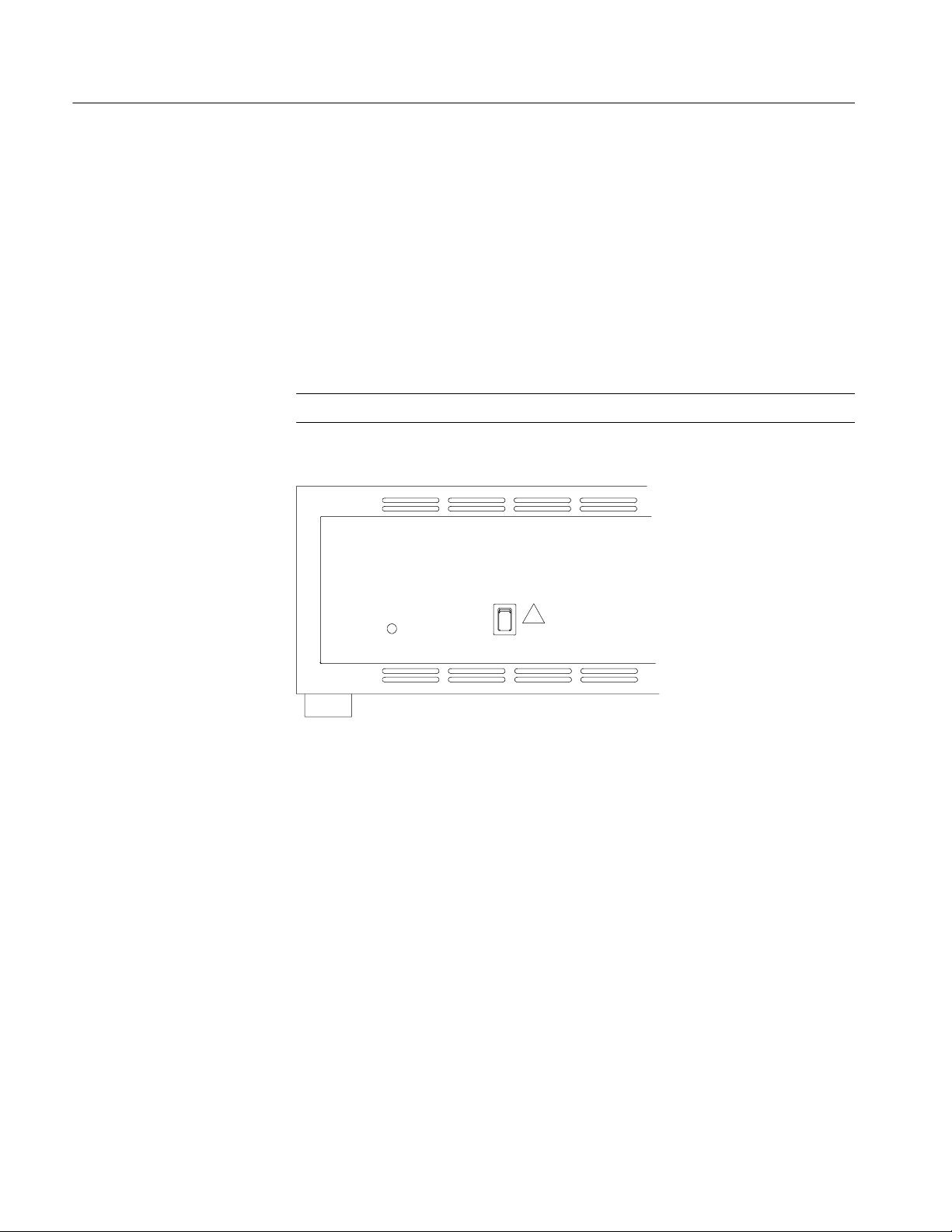
The probe adapter is configured for the AGP8X mode from the factory. To use
either the AGP8X or the AGP4X modes, follow these steps:
1. Change the mode switch on the front of the preprocessor unit to AGP4X
mode or AGP8X mode (see Figure 1--2).
2. Power the probe adapter off and on.
3. Reset the target system while in the chosen mode.
NOTE. The AGP4X mode is available only for AGP3.0 target systems.
8X mode
i
4X mode
The “i” indicates a reminder to
reset the target system.
Figure 1- 2: Switch for AGP8X or AGP4X mode
1- 6
TMS809 AGP 3.0 Bus Support
Page 25
Connecting the Logic Analyzer to a Target System
We recommend that you use the Interposer probe head to connect the logic
analyzer to the target system. If the target system functions improperly using the
Interposer board, use the Backside probe head. If you use the B ackside probe
head, you need to remove the target system from the case that houses it.
NOTE. For storage and shipping, retain the cardboard cartons and packing
material that is shipped with the probe adapter.
WARNING. To prevent harm to yourself or damage to the preprocessor unit, do
not open the preprocessor unit. There are no operator serviceable parts inside
the preprocessor unit. Refer servicing of internal parts in the preprocessor unit
to Tektronix authorized personnel only. External parts may be replaced by
qualified service personnel.
Getting Started
Tools Required. Following is a list of required tools:
H Nut driver (1/4 in) to remove the extension nuts from the Backside board
assembly
H Phillips screwdriver (P2) to remove a probe head and to secure the Backside
probe head
H Flat blade screwdriver to install the probe heads
Optional Tools. A torque wrench helps to ensure reliable connections by meeting
the nominal torque values listed in these instructions.
See the following pages for these procedures:
H Interposer probe head installation (see page 1--8)
H Probe-head removal (see page 1--11)
H Backside probe head installation (see page 1--12)
WARNING. To prevent burns, forced air cooling is required across the probe
adapter to maintain a temperature below 105
temperature for the components and the probe adapter.
°C (220 °F). You must verify this
TMS809 AGP 3.0 Bus Support
1- 7
Page 26
Getting Started
CAUTION. To prevent static damage to the power pod, probe adapter, probes, and
module, handle components only in a static-free environment.
Always wear a grounding wrist strap, heel strap, or similar device while
handling the bus and probe adapter.
Connecting the Interposer
Probe Head
For the first-time connection of the Interposer probe head to the AGP 3.0 signals
in the target system, follow these steps:
NOTE. If you are reconnecting the Interposer probe head, see Reconnecting the
Interposer Probe Head on page 1--9.
1. Power off the target system. It is not necessary to power off the logic
analyzer.
2. Power off any probe adapters that may be attached to your target system. If
the Backside probe head is attached, follow the instructions for Removing a
Probe Head on page 1--11.
3. To discharge any stored static electricity, touch the ground connector located
on the back of the logic analyzer.
4. Place the preprocessor unit on a horizontal, static free surface.
NOTE. When debugging an AGP Pro 1.5 V compatible graphic card, we
recommend that you use the backside probe adapter.
5. Remove the AGP 3.0 bus card from the target system.
1- 8
6. Connect the Interposer probe head to the target system as shown in
Figure 1--3.
7. Connect the AGP 3.0 bus card to the Interposer probe head.
CAUTION. To prevent damage to the probe adapter or target system when pow er
is applied, connect the target system to the probe adapter properly.
TMS809 AGP 3.0 Bus Support
Page 27
AGP 3.0 bus card
AGP 3.0 Interposer probe
head (includes Front End
board and Backside board)
Getting Started
AGP 3.0 bus connector
Reconnecting the
Interposer Probe Head
Target system
Figure 1- 3: Connect the Interposer probe adapter to the AGP 3.0 bus connector
WARNING. To prevent burns, forced air cooling is required across the probe
adapter to maintain a temperature below 105
°C (220 °F). You must verify this
temperature for the components and the probe adapter.
8. Apply forced air cooling across the probe head.
Before you begin to reconnect the Interposer probe head, check that no probe
adapters are attached to the preprocessor unit and that the access panel on top of
the preprocessor unit has been removed.
NOTE. When debugging an AGP Pro 1.5 V compatible graphic card, we
recommend that you use the backside probe adapter.
1. Power off the preprocessor unit.
TMS809 AGP 3.0 Bus Support
2. Power off the target system. You do not need to power off the logic analyzer.
3. Discharge the stored static electricity by touching the ground connector
located on the back of the logic analyzer.
1- 9
Page 28
Getting Started
4. Connect the three small boards (attached to the probe-head cables), matching
A to A, B to B, and C to C, to the Logic board. Access to the small board
connections is through the access panel on top of the preprocessor unit (see
Figure 1--4).
S2_E_DIS
S2_C_DIS
S2_A_DIS
S2_D_DIS
M_C_DIS
M_A_DIS
S_C_DIS
S2_D_DIS
S2_E_DIS
S2_A_DIS
M_E_DIS
M_D_DIS
M_A_TMG
M_C_TMG
Access panel
M_D_TMG
Screws (6)
Figure 1- 4: Preprocessor unit and access panel
5. Using a Phillips screwdriver, install the six screws into the three small
boards (torque to 4 in-in/lb).
6. Using a Phillips screwdriver, attach the three power cables and the three
screws (torque to 6 in/lb) to the Front End board (see Figure 1--5).
CAUTION. To prevent damage to the probe adapter, check that the power cables
are reattached to the Front End board correctly.
Front End board
1- 10
Black to GND
Yellow to --5 V
Redto+5V
Figure 1- 5: Attach the power cables
7. Hand start the screws that attach the access panel to the top of the preproces-
sor unit.
TMS809 AGP 3.0 Bus Support
Page 29
Getting Started
8. Using a Phillips screwdriver, tighten the screws (torque to 4 in/lb) in the
access panel (see Figure 1--4).
9. Connect the Interposer probe head to the target system (go to step 6 on
page 1--8 and complete the steps).
Removing a Probe Head
If you need to remove a probe head, follow these steps:
CAUTION. To prevent static damage, handle these components only in a
static-free environment. Static discharge can damage the probe adapter, the
probes, and the logic analyzer module.
Always wear a grounding wrist strap, heel strap, or similar device while
handling the probe adapter.
1. Power off the probe adapter and unplug the AC power cord on the preproces-
sor unit from the wall. The probe adapter power switch is located on the
back of the preprocessor unit. It is not necessary to power off the logic
analyzer.
2. Using a Phillips screwdriver, remove the screws from the access panel
located on top of the preprocessor unit (see Figure 1--4). Set the access panel
aside.
3. Using a Phillips screwdriver, remove the screws from the three small boards
(attached to the probe-head cables). Access to the small boards is through the
access panel on top of the preprocessor unit.
4. Disconnect the small boards from the Logic board.
TMS809 AGP 3.0 Bus Support
NOTE. Do not remove the power cables from the preprocessor unit.
5. Remove the three screws and the three power cables from the Front End
board. Set the screws aside for use later.
Interposer probe head only — Disconnect the Interposer probe head from the
target system. To properly store the Interposer probe head for use later, see
Storage on page 1--26. To store the AGP 3.0 bus card, refer to the AGP 3.0
bus card information from the manufacturer. To reinstall the Interposer probe
head, go to Reconnecting the Interposer Probe Head on page 1--9.
Backside probe head only — To complete the removal procedure for the
Backside probe head, follow these steps:
6. Using a Phillips screwdriver, remove the two screws from the center two
holes on the Front End board assembly (see Figure 1--8 on page 1--17).
1- 11
Page 30
Getting Started
7. Remove the Front End board assembly from the Backside board assembly.
8. Using a nut driver, carefully remove the four extension nuts from the
Backside board assembly (see Figure 1--7 on page 1--16).
9. Remove the Backside board from the mounting plate on the target system.
NOTE. We recommend that you do not remove the mounting plate after it is
attached to the target system.
To properly store the Backside probe head for use later, see Storage on
page 1--26.
Connecting the Backside
Probe Head
To connect the Backside probe head to the signals on the target system, follow
these steps:
1. Power off the target system. It is not necessary to power off the logic
analyzer.
CAUTION. To prevent static damage, handle these components only in a
static-free environment. Static discharge can damage the probe adapter, the
probes, and the logic analyzer module.
Always wear a grounding wrist strap, heel strap, or similar device while
handling the bus.
2. To discharge the stored static electricity, touch the ground connector located
on the back of the logic analyzer.
3. Disconnect any attached probe adapters. See Removing a Probe Head on
page 1--11.
NOTE. Use an antistatic cushion to protect the components on the underside of
the target system, because you will be applying pressure to the AGP 3.0 board.
1- 12
4. Place the target system on a horizontal, static-free surface (the back of the
AGP 3.0 connector must be visible).
TMS809 AGP 3.0 Bus Support
Page 31

Getting Started
CAUTION. To prevent replacing the mounting plate due to misalignment, place
the mounting plate carefully on the back of the AGP 3. 0 connector. You can use
the mounting plate adhesive strips only once.
After adhering the mounting plate to the target system, we recommend that you
allow the adhesive strips to cure for 72 hours before attaching the Backside
probe head to the target system. The adhesive strips are at 80% cure after 24
hours.
We recommend that you do not remove the mounting plate after it is attached to
the target system.
5. Retrieve the mounting plate and the positioning block from the supplied
standard accessories (see Figure 1--6).
6. Position the mounting plate near the top of the positioning block (see
Figure 1--6).
TMS809 AGP 3.0 Bus Support
1- 13
Page 32

Getting Started
7. Without removing the adhesive protector strips, test steps 9 and 10 to verify
that obstructions do not exist and the mounting plate seats flush to the
surface of the board. If there are obstructions, remove them.
CAUTION. To prevent damage to the target system, the stud heads on the
mounting plate must avoid target-system circuitry (see Figure 1--6). If they do
not, use the Interposer probe head.
Positioning block
Mounting plate
Center stud
Remove adhesive protectors
AGP 3.0 pins (on the
back of the AGP 3.0
connector.)
Slide down
Center holes
(for center stud)
Target system
Remove
positioning block
Stud head
Positioning block
looking underneath
Pin holes
(four on each end)
Studs (4)
Mounting plate
1- 14
Before
After
Figure 1- 6: Attaching the mounting plate to the target system
8. Remove the adhesive protector strips from the mounting plate
(see Figure 1--6).
9. Seat the positioning block on the back of the AGP 3.0 connector. Key the
center stud to the hole on the bottom of the positioning block and align the
eight pin holes on the positioning block to the pins on the AGP 3.0
connector (see Figure 1--6).
TMS809 AGP 3.0 Bus Support
Page 33

Getting Started
10. When you have seated the positioning block on the AGP 3.0 connector, slide
the mounting plate into position. Securely adhere the mounting plate to the
back of the AGP 3.0 connector by pressing evenly over the entire surface.
11. After the mounting plate is attached, remove the positioning block from the
mounting plate. Discard the positioning block.
NOTE. For the first-time installation of the Backside probe head, you must
remove the Front End board from the Backside board by removing the two
screws and washers that attach the boards before continuing with the following
steps (see Figure 1--8 on page 1--17).
12. Key the four small holes on the Backside board assembly to the four
mounting-plate studs. Guide the Backside board assembly into place on top
of the mounting plate (see Figure 1--6 on page 1--14).
13. Insert the four extension nuts into the larger holes on the Backside board
assembly (see Figure 1--7).
CAUTION. To avoid damage to the studs on the mounting plate, finger tighten the
extension nuts (torque to 1 in/lb).
14. Locate the four tab holes on the Front End board assembly (the side without
the heatsink).
15. Insert the four tabs on the Backside board assembly into the four tab holes
on the Front End board assembly, press into place.
TMS809 AGP 3.0 Bus Support
1- 15
Page 34

Getting Started
Tab holes (4)
Front End
board assembly
Insert each Tab on the
Backside board
assembly into the
holes on the Front End
assembly.
Tabs (4)
Figure 1- 7: Attaching the Front End board assembly
Heatsink
Extension nuts (4)
Backside board
assembly
1- 16
NOTE. The two ribbon cables are captured between the two assemblies when the
Backside probe head is properly installed.
TMS809 AGP 3.0 Bus Support
Page 35

Getting Started
16. Align the center two holes on the Front End board to the holes on the
Backside board. Heatsinks are visible when the Front End board is attached.
Install two screws and two washer into the center two holes of the Front End
board.
17. Using a flat-blade screwdriver, attach the Front End board assembly to the
Backside board assembly, Torque to 5 in/lb (see Figure 1--8).
Front End board
assembly
Because the Front End board can be
CAUTIONl
Front End board
assembly
Backside board
assembly
attached from either side, the power
cables must be visible when attaching
the Front End board assembly to the
Backside board assembly
Mounting plate
Figure 1- 8: Assembled Backside probe head
Install two
screws
Target system
TMS809 AGP 3.0 Bus Support
1- 17
Page 36

Getting Started
18. Using a flat-blade screwdriver, install three screws and three power cables to
the Front End board (see Figure 1--8).
CAUTION. To prevent damage to the probe adapter, check that the three power
cables are attached to the Front End board correctly (see Figure 1--9).
Front End board
Black to GND
Yellow to --5 V
Redto+5V
Figure 1- 9: Attach the power cables
19. Connect the three small boards (attached to the probe-head cables), matching
A to A, B to B, and C to C, to the Logic board. Access to the small boards is
through the access panel on top of the preprocessor unit (see Figure 1--10).
S2_E_DIS
S2_C_DIS
S2_A_DIS
S2_D_DIS
M_C_DIS
M_A_DIS
S_C_DIS
S2_D_DIS
S2_E_DIS
S2_A_DIS
M_E_DIS
M_D_DIS
M_A_TMG
M_C_TMG
Access panel
M_D_TMG
Screws (6)
1- 18
Figure 1- 10: Preprocessor unit and access panel
TMS809 AGP 3.0 Bus Support
Page 37

Getting Started
20. Using a Phillips screwdriver, install six screws into the three small boards.
21. Position the access panel on top of the preprocessor unit and hand start the
screws.
22. Using a Phillips screwdriver, tighten the screws in the access panel (torque to
4 in/lb).
WARNING. To prevent burns, forced air cooling is required across the probe
adapter to maintain a temperature below 105
°C (220 °F). You must verify this
temperature for the components and the probe adapter.
23. Apply forced air cooling across the probe head.
TMS809 AGP 3.0 Bus Support
1- 19
Page 38

Getting Started
Connecting P6434 or
P6860 Probes
Mictor connectors on the probe adapter may be configured for timing or
disassembly software functions.
NOTE. For more detailed information about how to attach a P6860 probe or the
mictor adapters, we recommend that you refer to the logic analyzer online help
or the P6860 probe manual listed on page 1--2. Then proceed with connecting
the probes for the minimum configuration for disassembly and timing software in
this section.
To view the P6860 probe and mictor adapters, see Figure 1--13 on page 1--22.
For reference, Figure 1--11 shows the module configuration for the Slave 2,
Master, and Slave modules.
Slave 2 Master Slave
1- 20
Figure 1- 11: Configuration of the slave 2, master, and slave modules
Disassembly. Following is the minimum probe configuration for disassembly
software.
1. Match the A, D, C, and E probes from the Slave2 module with the corre-
sponding S2_A_DIS, S2_D_DIS, S2_C_DIS, and S2_E_DIS probe
connectors labels on the preprocessor unit. Align the pin 1 indicator on the
probe label with the pin 1 indicator of the connector on the preprocessor unit.
TMS809 AGP 3.0 Bus Support
Page 39

Getting Started
CAUTION. To prevent damage to the probe and preprocessor unit, always
position the probe perpendicular to the mating connector with pin 1s aligned
and then gently connect the probe. Incorrect handling of the probe while
connecting to or disconnecting from the preprocessor unit can damage the probe
or the mating connector on the preprocessor unit.
2. Position the probe tip perpendicular to the mating connector, and gently
connect the P6434 probe (see Figure 1--12). To attach a P6860 probe, skip
steps 2 and 3 and refer to the probe manual listed on page 1--2.
3. When connected, push down on the latch releases on the probe to set the latch.
Push down to latch after
probe is connected
Push down to latch after
probe is connected
P6434 probe
Pin 1
Pin 1
Figure 1- 12: Operating the P6434 probe latches
4. Match the A, D, C, and E probes from the Master module with the corre-
sponding M_A_DIS, M_D_DIS, M_C_DIS, and M_E_DIS probe connectors labels on the preprocessor unit. Align the pin 1 indicator on the probe
label with the pin 1 indicator of the connector on the preprocessor unit.
5. Repeat steps 2 and 3 to correctly connect the probes.
6. Match the A, D, C, and E probes from the Slave module with the corre-
sponding S_A_DIS, S_D_DIS, S_C_DIS and S_E_DIS probe connector
labels on the preprocessor unit. Align the pin 1 indicator on the probe label
with pin 1 of the connector on the preprocessor unit (see Figure 1--12).
TMS809 AGP 3.0 Bus Support
7. Repeat steps 2 and 3 to correctly connect the probes.
1- 21
Page 40

Getting Started
Timing. Following is the minimum probe configuration for timing software.
1. Match the A, D, and C probes from the Master module with the correspond-
ing M_A_TMG, M_D_TMG, and M_C_TMG probe connectors labels on
the preprocessor unit. Align the pin 1 indicator on the probe label with the
pin 1 indicator of the connector on the preprocessor unit.
CAUTION. To prevent damage to the probe and preprocessor unit, always
position the probe perpendicular to the mating connector and then gently
connect the probe. Incorrect handling of the probe while connecting to or
disconnecting from the preprocessor unit can damage the probe or the mating
connector on the preprocessor unit.
2. Position the probe tip perpendicular to the mating connector, and gently
connect the probe (see Figure 1--12). To attach a P6860 probe, skip steps 2
and 3 and refer to the probe manual listed on page 1--2.
3. When connected, push down on the latch releases on the probe to set the
latch.
Figure 1--13 shows probes using mictor adapters with compression footprints.
For more information about these probes, refer to page 1--2.
P6860
P6434
Compression
adapter
Mictor adapter
Mictor adapter
1- 22
Figure 1- 13: Probes with mictor adapters
TMS809 AGP 3.0 Bus Support
Page 41

Getting Started
Applying Power
To apply power to the AGP 3.0 probe adapter and target system, follow these
steps:
WARNING. To prevent harm to yourself or damage to the preprocessor unit, do
not open the preprocessor unit. There are no operator serviceable parts inside
the preprocessor unit. Refer servicing of internal parts in the preprocessor unit
to Tektronix authorized personnel only. External parts may be replaced by
qualified service personnel.
1. Check that the power switch on the preprocessor unit is in the off position. If
powered off, the zero (0) is visible on the power switch.
2. Plug the AC power cord into the IEC connector on the back of the preproces-
sor unit.
3. Plug the AC power cord into an electrical outlet that you know is working
properly.
4. Power on the preprocessor unit. A green, power-on LED lights on the front
of the preprocessor unit, indicating that the probe is active. If the LED does
not light, see Verifying Probe Operation on page 1--23.
5. Power on the target system.
Removing Power
To remove power from the probe adapter, follow these steps:
1. It is not necessary to power off the target system or logic analyzer.
2. Power off the probe adapter at the back of the preprocessor unit.
Verifying Probe Operation
If you have trouble using the AGP 3.0 probe adapter to acquire data from the
target system, use the following check list to ensure that the probe adapter and
probe-head cables are working correctly.
WARNING. To prevent harm to yourself or damage to the preprocessor unit, do
not open the preprocessor unit, except to verify probe head cable connections.
There are no operator serviceable parts inside the preprocessor unit. Refer
servicing of internal parts in the preprocessor unit to Tektronix authorized
personnel only. External parts may be replaced by qualified service personnel.
1. Check that power is supplied to the preprocessor unit by observing the green
LED on the front of the case. If the LED is not lighted:
TMS809 AGP 3.0 Bus Support
1- 23
Page 42

Getting Started
H Check that the power switch on the back of the preprocessor unit is
powered on. If powered off, a zero (0) is visible on the switch.
H Check that the AC power cord is plugged into an electrical outlet that
you know is working properly.
H Check if the fans in preprocessor unit are rotating.
H Check the probe head cable connections through the opening in the top
of the preprocessor unit (see Figure 1--14).
H If the LED is still not lighted, call a Tektronix application engineer.
2. Check that signals are passing through the mictor connectors by using the
following procedure:
a. Go to the setup menu and select “show activity”.
b. Visually verify from the display that signals are transitioning on each
mictor connector.
c. If the signals are not transitioning, wiggle the mictor connector on top of
the preprocessor unit slightly to check that it is fully seated.
d. If the channels never transition:
H Check the mictor probe for bent contacts.
H Check the preprocessor unit for bent mictor contacts.
If the preceding bulleted items did not correct the problem, replace the
existing mictor probe with a new mictor probe.
e. If the signals are still not transitioning, disconnect the mictor probe from
that socket in the preprocessor unit. Then plug the mictor probe into a
socket that is transitioning signals.
S2_E_DIS
S2_C_DIS
S2_A_DIS
S2_D_DIS
M_C_DIS
M_A_DIS
S_C_DIS
S2_D_DIS
S2_E_DIS
S2_A_DIS
M_E_DIS
M_D_DIS
M_A_TMG
M_C_TMG
M_D_TMG
1- 24
Access panel
Figure 1- 14: Preprocessor unit and access panel
TMS809 AGP 3.0 Bus Support
Page 43

Replacing the Pogo Pin Assembly (Backside Board)
To replace the Pogo pin assembly, follow these steps:
1. Power off the target system. It is not necessary to power off the logic
analyzer.
2. Power off the probe adapter at the back of the preprocessor unit.
3. Disconnect the Backside probe head from the target system. Go to Removing
a Probe Head on page 1--11. Start with step 1, then skip to step 6 and end at
step 9.
CAUTION. To prevent the Pogo pins from falling out of the assembly during
removal, grasp the top and bottom of the assembly during removal. Before
releasing the assembly, check that all four spiral pins are attached to the Pogo
pin assembly. Reinstall any missing spiral pins.
T o prevent damage to the target system, position the Pogo pin assembly as
shown in Figure 1--15.
Getting Started
4. After the Backside probe head is disconnected, remove the two screws from
the Pogo pin assembly (see Figure 1--15). Remove the Pogo pin assembly.
5. Using the spiral pins on the Pogo pin assembly as keys, slide the new Pogo
pin assembly onto the Backside board.
6. Using a Phillips screwdriver and two screws, align and attach the Pogo pin
assembly (torque to 4 in/lb) to the Backside board.
Flat head
screws (2)
Align 4 spiral
pins to holes
Pogo pin assembly
Align holes
TMS809 AGP 3.0 Bus Support
Backside board
Figure 1- 15: Replacing the Pogo pin assembly on the Backside board
1- 25
Page 44

Getting Started
Storage
The storage instructions describe short- and long-term storage of the probe head,
cables, and preprocessor unit.
CAUTION. To prevent damage to the sensitive probe-head cables, dress the cables
to not pinch or contact any sharp objects. When you fold the cables use a
minimum radius of 0.25 (0.64 cm) at the fold.
Short-Term Storage
Long-Term Storage
For short-term storage follow these steps:
1. Power off the probe adapter. You can leave the logic analyzer powered on.
2. Disconnect the probe head. See Removing a Probe head on page 1--11 for the
Interposer probe head and for the Backside probe head.
3. Place the Interposer probe head in the black shipping carton and store with
the preprocessor unit. If the shipping carton is not available, wrap pink
antistatic bubble wrap around the probe head. Store the Backside probe head
in an antistatic bag.
For long-term storage; use the existing cardboard carton, black carton, and
packaging, and follow these steps:
1. Power off the probe adapter. You can leave the logic analyzer powered on.
2. Disconnect the preprocessor unit from the logic analyzer by removing the
P6434 probes from the top of the preprocessor unit.
3. Unplug the AC power cord from the IEC connector on the back of the
preprocessor unit.
4. Disconnect the probe head. See Removing the Probe head on page 1--11 for
the Interposer probe head and for the Backside probe head.
1- 26
5. Place the preprocessor unit inside the antistatic bag.
6. Place the Interposer probe head in the black carton and fold the carton over
the top of the preprocessor unit. Store the unused probe head in an antistatic
bag.
CAUTION. To prevent damage to the sensitive probe-head cables, dress the cables
to not pinch or contact any sharp objects. When you fold the cables use a
minimum radius of 0.25 (0.64 cm) at the fold.
7. Place the foam end caps on both sides of the preprocessor unit. The
depression on the foam end caps is positioned up.
TMS809 AGP 3.0 Bus Support
Page 45

Care and Maintenance
Getting Started
8. Place the preprocessor unit inside the cardboard carton.
9. Place the cardboard accessory tray on top of the foam end caps. Close the
carton.
Before cleaning this product, read the following information:
CAUTION. Static discharge can damage the probe adapter, the probes, and the
module. To prevent static damage, handle components only in a static-free
environment.
The TMS809 AGP 3.0 probe adapter does not require scheduled or periodic
maintenance. However, to maintain good electrical contact and efficient heat
dissipation, keep the probe adapter free of dirt, dust, and contaminants. When not
in use, store the probe adapter in the original shipping bags and cardboard
cartons (see Storage on page 1--26).
External Cleaning Only
Clean dirt and dust with a soft bristle brush. F or more extensive cleaning, use
only a damp cloth moistened with deionized water; do not use any other
chemical cleaning agents.
WARNING. To prevent harm to yourself or damage to the preprocessor unit, do
not open the preprocessor unit for cleaning. There are no operator serviceable
parts inside the preprocessor unit. Refer servicing of internal parts in the
preprocessor unit to Tektronix authorized personnel only. External parts may be
replaced by qualified service personnel.
TMS809 AGP 3.0 Bus Support
1- 27
Page 46

Getting Started
Shipping the Probe Adapter
To commercially transport the TMS809 AGP 3.0 probe adapter, package as
follows:
1. Use the existing cardboard shipping cartons. If the existing shipping cartons
are not available, use a double-walled, corrugated cardboard shipping carton
with dimensions that are three inches (7.62 cm) larger on each side and top
of the carton than the probe adapter.
2. If you are shipping the probe adapter to a Tektronix service center for
Warranty service, attach a tag to the probe adapter showing the following:
H Owner’s name and address
H Name of a person who can be contacted
H Probe adapter type and serial number
H Description of the problem
3. Place the preprocessor unit in the antistatic bag.
4. Place the probe head and cables in the black shipping carton, and fold the
black shipping carton over the top of the preprocessor unit.
CAUTION. To prevent damage to the sensitive probe-head cables, dress the cables
to not pinch or contact any sharp objects. When you fold the cables use a
minimum radius of 0.25 (0.64 cm)at the fold.
5. Place the foam end caps on both sides of the preprocessor unit. The
depression on the foam end caps are positioned up.
If the foam end caps are not available, tightly pack dunnage or urethane foam
between the cardboard carton and the probe adapter allowing 3 inches
(7.62 cm) on each side to cushion the probe adapter.
6. Place the preprocessor unit inside the cardboard carton.
7. Place the cardboard accessory tray on top of the probe adapter. Close and
tape the cardboard carton.
8. Ship the probe adapter.
1- 28
TMS809 AGP 3.0 Bus Support
Page 47

Operating Basics
Page 48

Page 49

Setting Up the Software
This section provides information on how to set up the TMS809 AGP 3.0 Bus
software on any Tektronix logic analyzer along with the following topics:
H Channel group definitions and symbol table overview
H Support package setups
H Disassembled Data
Basic information for general tasks and functions are described in the Tektronix
logic analyzer online help or the Tektronix logic analyzer user manual.
Before you acquire and display disassembled data, you must load the support
and specify setups for clocking as described in the information on basic
operations. The support provides default values for the setups, but you can
change them as needed.
Installing the Software
NOTE. Before you install any software, we recommend that you verify the bus
support software is compatible with the logic analyzer software.
To install the TMS809 software on your Tektronix logic analyzer, follow these
steps:
1. Insert the floppy disk in the disk drive.
2. Select the Windows Start button, point to Settings, and select Control Panel.
3. In the Control Panel window, double-click Add/Remove Programs.
4. Follow the instructions on the screen for installing the software from the
floppy disk.
To remove or uninstall software, follow the above instructions and select
Uninstall. You must close all windows before you uninstall any software.
TMS809 AGP 3.0 Bus Support
2- 1
Page 50

Setting up the Software
Support Package Setups
The TMS809 AGP 3.0 software package installs three setup support files. Each
setup provides different clocking and display options. All channels are displayed
as active high.
AGP3_8X Setup
AGP3_4X Setup
AGP3_T Setup
This setup provides disassembly support for the AGP3_8X bus.
This setup provides disassembly support for the AGP3_4X bus.
NOTE. To use the AGP4X mode see Configuring the Probe Adapter on page 1--6.
This setup provides timing support.
Channel Group Definitions
The TMS809 AGP 3.0 software package automatically defines channel groups
for each installed support setup. The channel groups for the AGP 3.0 software
support are SBA[7:0]#, Command, AD[31:0], C#_BE[3:0], Control, Status, and
Misc. If you want to know which signal is in which channel group, refer to the
channel assignment tables beginning on page 3--25.
For additional information on bus signals for the probe adapter, see page 3--43.
Symbol Tables
2- 2
For channel groups with an associated symbol table file, you can set the display
radix to Symbolic and select the proper symbol table by using the column
properties dialog in the listing window display.
Symbol Tables begin on page 3--1. Following is a list of the symbol table file
names:
AGP3_Command
AGP3_Status
AGP3_Control
AGP3_SBA_Cmd
TMS809 AGP 3.0 Bus Support
Page 51

Acquiring and Viewing Disassembled Data
This section describes how to acquire data and view it dissembled. For additional
information about channel tables see page 3--5.
Setting up the Software
Acquiring Data
Clocking
Custom Clocking Mode
After you load the AGP 3.0 bus support package and choose a clocking option,
you are ready to acquire and disassemble data.
If you have any problems acquiring data, refer to information on basic operations, logic analyzer online help, or Appendix A: Error Messages and Disassem-
bly Problems in the logic analyzer user manual.
The module acquires AGP 3.0 signals using the TMS809 AGP 3.0 bus support
software and probe adapter .
For correct disassembly, do not use the Internal or External clocking modes. The
logic analyzer online help describes in more detail how to use these clock
selections for general purpose analysis.
H Internal clocking (used for timing) is based on the clock generated by a
Tektronix logic analyzer. You can configure the clock rate from 50 ms down
to 4 ns. For the TLA7XX, you can configure the clock rate to 2 ns.
H External clocking is used when you configure the clocking of data based on
logical combinations of clocks and qualifiers.
A special clocking program is loaded to the module every time you load the
AGP 3.0 bus support package. This special clocking is called Custom.
TMS809 AGP 3.0 Bus Support
With Custom clocking, the module logs in signals from multiple groups of
channels at different times as they become valid on the AGP 3.0 bus. The
module then sends all the logged-in signals to the trigger machine and to the
memory of the module for storage.
Custom Clocking Menu Options. The only custom clocking option available is
Clock-by-Clock.
Clock-by-Clock. This custom clocking option acquires all channels on every
rising edge of the AGP CLK signal, except during reset, where only one sample
is acquired. Invalid phases are represented as dashes.
2- 3
Page 52

Setting up the Software
Active Cycles Only. Active Cycles Only mode clocks in only those cycles which
have valid data on the AD[31:0], SBA[7:0], C/BE[3:0]#, and the ST[2--0] buses.
This clocking mode is enabled only after you set up menu definitions in the
Storage definition window (see Figure 2--1). Use the following procedure:
1. Load the support package.
2. From the system window, select the logic analyzer Trigger
3. Select the Power Trigger tab.
4. In the Storage menu, select Conditional.
5. From the Storage Definition window, select the If button and either Channel
or Group from the menu.
6. For each row in the Storage Definition window, select the menu definition
shown in Figure 2--1.
NOTE. When AGP4X mode is enabled the same menu definitions are selected,
except channel 4X/PCI#_AD and omit groups 4--SBA[7:0]# and 6_SBA[7:0]#.
button.
Figure 2- 1: Select these definitions for AGP8X
2- 4
TMS809 AGP 3.0 Bus Support
Page 53

Setting up the Software
Viewing Disassembled
Data
You can view acquired data in two formats: Listing and Waveform. The
information on basic operations describes how to select the disassembly display
formats.
Table 2--1 shows the waveforms that are displayed when using the AGP 3.0
support package.
Table 2- 1: Waveform displays
AGP 3.0
AGP 3.0 support
signal name
CLK X X
AD_STBF0 -- X
AD_STBS0 -- X
AD[15--0] -- X
AD_STBF1 -- X
AD_STBS1 -- X
AD[31--16] -- X
[0--7]_AD[31--0] X --
disassembly
support
AGP3_T
support
Command X --
SBA[7:0] -- X
[0--7]_SBA[7:0] X --
SBA_STBF -- X
SBA_STBS -- X
C#_BE[3:0] -- X
[0--7]_C#_BE[3:0] X --
ST2 X X
ST1 X X
ST0 X X
FRAME# X X
IRDY# X X
TRDY# X X
RBF# X X
WBF# X X
STOP# X X
DEVSEL# X X
TMS809 AGP 3.0 Bus Support
REQ# X X
2- 5
Page 54

Setting up the Software
Table 2- 1: Waveform displays (Cont.)
AGP 3.0
AGP 3.0 support
signal name
disassembly
support
AGP3_T
support
GNT X X
RESET#
1#
1
X X
Indicates that the signal is asserted low
Table 2--2 lists the default display radix for the AGP 3.0 channel groups.
Table 2- 2: Default display radix
Group name
State default
display radix
Disassembly default
display radix
0/ SBA[7:0]# BIN OFF
1_SBA[7:0]# BIN OFF
2_SBA[7:0]# BIN OFF
3_SBA[7:0]# BIN OFF
4_SBA[7:0]#
5_SBA[7:0]#
6_SBA[7:0]#
7_SBA[7:0]#
SBA D/O
Mnemonics D/O
}
}
}
}
BIN OFF
BIN OFF
BIN OFF
BIN OFF
{
{
SYM
TEXT
0/PCI_AD[31:0] HEX OFF
1_AD[31:0] HEX OFF
2_AD[31:0] HEX OFF
3_AD[31:0] HEX OFF
4_AD[31:0]
5_AD[31:0]
6_AD[31:0]
7_AD[31:0]
Addr/Data D/O
}
}
}
}
HEX OFF
HEX OFF
HEX OFF
HEX OFF
{
HEX
0/PCI_C#_BE[3:0] HEX OFF
1_C#_BE[3:0] HEX OFF
2_C#_BE[3:0] HEX OFF
3_C#_BE[3:0] HEX OFF
4_C#_BE[3:0]
5_C#_BE[3:0]
6_C#_BE[3:0]
7_C#_BE[3:0]
}
}
}
}
HEX OFF
HEX OFF
HEX OFF
HEX OFF
2- 6
TMS809 AGP 3.0 Bus Support
Page 55

Table 2- 2: Default display radix (Cont.)
Setting up the Software
Group name
PCI Cmd D/O
Control SYM OFF
Command SYM OFF
Status SYM OFF
Misc HEX OFF
{
D/O: Disassembly only
}
Signal omitted on 4X support
Viewing an Example of Disassembled Data
A demonstration system file (or demonstration reference memory) is provided on
your software support disc. This example shows you how the bus cycles and
instruction mnemonics look when they are disassembled. Viewing the system
file is not a requirement for preparing the module for use and you can view it
without connecting the logic analyzer to the target system.
State default
display radix
{
Disassembly default
display radix
TEXT
TMS809 AGP 3.0 Bus Support
2- 7
Page 56

Setting up the Software
2- 8
TMS809 AGP 3.0 Bus Support
Page 57

Reference
Page 58

Page 59

Symbol Tables
This section contains symbol tables Tables 3--1 through 3--4.
Table 3--1 lists the name, bit pattern, and meaning for the symbols in the file
AGP3_Command, the Command channel group symbol table.
Table 3- 1: AGP3_Command symbol table definitions
Command group value
FRAME C#BE2
FRAME_L C#BE1
Symbol
PCI_Int_Ack 0 100 1111 PCI Interrupt Acknowledge
PCI_Special 0 100 1110 PCI Special Command
PCI_I/O_Rd 0 100 1101 PCI Input/Output Read
PCI_I/O_Wr 0 100 1100 PCI Input/Output Write
PCI_Mem_Rd 0 100 1001 PCI Memory Read
PCI_Mem_Wr 0 100 1000 PCI Memory Write
PCI_Config_Rd 0 100 0101 PCI Configuration Read
PCI_Config_Wr 0 100 0100 PCI Configuration Write
PCI_Mem_Rd_Mul 0 100 0011 PCI Memory Read Multiple
PCI_Ext_Addr 0 100 0010 PCI Extended Address
PCI_Mem_Rd_Line 0 100 0001 PCI Memory Read Line
PCI_Mem_Rd_Inv 0 100 0000 PCI Memory Write and Invali-
PCI_I/O_R/W 0 100 110X PCI I nput/Output Read/Write
PCI_Mem_R/W 0 100 100X PCI Memory Read/Write
PCI_Config_R/W 0 100 010X PCI Configuration Read/Write
PCI_Cmd 0 100 XXXX Any PCI Command
~ 1 100 XXXX PCI data
-- 1 XXX XXXX Reserved/Undefined
IRDY 8X/PCI#_AD_D C#BE0
C#BE3
Description
date
TMS809 AGP 3.0 Bus Support
3- 1
Page 60

Symbol Tables
Table 3--2 lists the name, bit pattern, and meaning for the symbols in the file
AGP3_Status, the Status channel group symbol table.
Table 3- 2: AGP3_Status symbol table definitions
Status group value
ST2
ST1
Symbol
-- 1 XXX Grant Not Asserted
Grant 1 111 Transaction Request
Read 1 000 Read Transaction
Write 1 010 Write Transaction
Calibrate 1 110 Calibration Cycle
Rd/Wr 1 0X0 Read or Write Transaction
Reserved 1 XXX Reserved Status Code
GNT# ST0
Description
Table 3--3 lists the name, bit pattern, and meaning for the symbols in the file
AGP3_Control, the Control channel group symbol table.
Table 3- 3: AGP3_Control symbol table definitions
Control group value
RBF GNT IRDY
SERR FRAME TRDY
Symbol
RST# PERR FRAME_L DEVSEL
PME# PAR 8X/PCI#_AD_D STOP
Reset 0X XXXX XXXXX XXXX Reset
Sys_Err 1X X1XX XXXXX XXXX System Error
Par_Err 1X XX1X XXXXX XXXX Parity Error
PCI_Cmd 1X XXXX XX100 XXXX PCI Address
PCI_Data 1X XXXX XXX10 XXXX PCI Data
PCI_Abort 1X XXXX XXXX0 1X01 PCI Target Abort
PCI_Discon 1X XXXX XXXX0 1X11 PCI Target Disconnect
IRDY_TRDY 1X XXXX XXXXX 11XX IRDY/TRDY Asserted
IRDY 1X XXXX XXXXX 1XXX IRDY Asserted
TRDY 1X XXXX XXXXX X1XX TRDY Asserted
Rd_Buf_Fl 1X 1XXX XXXXX XXXX Read Buffer Full
Grant 1X XXXX X1XXX XXXX Grant Asserted
Request 1X XXXX 1XXXX XXXX Request Asserted
REQ
Description
3- 2
TMS809 AGP 3.0 Bus Support
Page 61

Table 3- 3: AGP3_Control symbol table definitions (Cont.)
Control group value
RBF GNT IRDY
RST# PERR FRAME_L DEVSEL
Symbol Description
Symbol Description
PME# PAR 8X/PCI#_AD_D STOP
SERR FRAME TRDY
Stop 1X XXXX XXXXX XXX1 Stop Asserted
Dev_Sel 1X XXXX XXXXX XX1X Device Select Asserted
Frame 1X XXXX XX1XX XXXX Frame Asserted
Pwr_Mgmt_Ev 10 XXXX XXXXX XXXX Power Management Event
PAR 1X XXX1 XXXXX XXXX Pipe Asserted
-- 11 000X 000XX 0000 Bus inactive
REQ
Symbol Tables
TMS809 AGP 3.0 Bus Support
3- 3
Page 62

Symbol Tables
Table 3--4 lists the name, bit pattern, and meaning for the symbols in the file
AGP3_SBA_Cmd, the SBA_Cmd channel group symbol table.
Table 3- 4: AGP3_SBA_Cmd symbol table definitions
SBA_Cmd group value
SBA7# SBA3#
SBA6# SBA2#
SBA5# SBA1#
Symbol
SYNC 1111 1110 synchronization cycle
NOP 1111 1111 NOP
Type_4 1110 XXXX Extended address
Type_3 1100 XXXX Upper address
Invalid 1101 XXXX Type 3, invalid reserved bit
Rd_Async 1000 000X Asynchronous Read
Reserved 1000 010X (formerly Rd_HP)
Reserved 1000 100X -- -- --
Rd_ISOCH 1000 110X Isochronous Read Command
Wr_Async 1001 000X Asynchronous Write
Reserved 1001 010X (formerly Wr_HP)
Wr_ISOCH_Unfncd 1001 100X Isochronous Write Unfenced
Wr_ISOCH_Fenced 1001 110X Isochronous Write Fenced
Reserved 1010 000X (formerly L_Rd_LP)
Reserved 1010 010X (formerly L_Rd_HP)
Flush 1010 100X Flush -- Similar to Read
Reserved 1010 110X -- -- --
Fence 1011 000X Fence
Reserved 1011 010X PCI -- Dual Address Cycle
Align_ISOCH 1011 100X Returns time offset of corelogic
Reserved 1011 110X -- -- --
Invalid 10XX XX1X Type 2, invalid reserved bit
Type_1 0XXX XXXX Lower address and command
Reserved 1111 0XXX Reserved command
SBA4# SBA0#
Description
(formerly Rd_LP)
(formerly Wr_LP)
(out--of--order completion)
(ordered completion)
3- 4
TMS809 AGP 3.0 Bus Support
Page 63

Channel Group Definition Tables
This section contains Channel Group Definition Tables 3--5 through 3--13 for
both the AGP3_8X and the AGP3_4X support packages with the following
exceptions.
NOTE. The following tables with channel names that are prefixed with 4_, 5_,
6_, and 7_, are not used in the AGP3_4X support setup.
Channel assignments shown in Tables 3--5 through 3--32 use the following
conventions:
H A pound sign (#) following a signal name indicates an active low signal.
H All signals are required by the support unless indicated otherwise.
H Channels are shown starting with the most significant bit (MSB) descending
to the least significant bit (LSB).
Table 3--5 lists the group definitions for the 7_AD[31:0] channel group. By
default, this group is displayed in hexadecimal.
Table 3- 5: 7_AD[31:0] channel group definitions
Bit
order
31 7_AD31
30 7_AD30
29 7_AD29
28 7_AD28
27 7_AD27
26 7_AD26
25 7_AD25
24 7_AD24
23 7_AD23
22 7_AD22
21 7_AD21
20 7_AD20
19 7_AD19
18 7_AD18
AGP 3.0 support
channel name
TMS809 AGP 3.0 Bus Support
3- 5
Page 64

Channel Group Definition Tables
Table 3- 5: 7_AD[31:0] channel group definitions (Cont.)
Bit
order
17 7_AD17
16 7_AD16
15 7_AD15
14 7_AD14
13 7_AD13
12 7_AD12
11 7_AD11
10 7_AD10
9 7_AD9
8 7_AD8
7 7_AD7
6 7_AD6
5 7_AD5
4 7_AD4
3 7_AD3
AGP 3.0 support
channel name
2 7_AD2
1 7_AD1
0 7_AD0
Table 3--6 lists the group definitions for the 6_AD[31:0] channel group. By
default, this group is displayed in hexadecimal.
Table 3- 6: 6_AD[31:0] channel group definitions
Bit
order
31 6_AD31
30 6_AD30
29 6_AD29
28 6_AD28
27 6_AD27
26 6_AD26
25 6_AD25
AGP 3.0 support
channel name
3- 6
TMS809 AGP 3.0 Bus Support
Page 65

Channel Group Definition Tables
Table 3- 6: 6_AD[31:0] channel group definitions (Cont.)
Bit
order
24 6_AD24
23 6_AD23
22 6_AD22
21 6_AD21
20 6_AD20
19 6_AD19
18 6_AD18
17 6_AD17
16 6_AD16
15 6_AD15
14 6_AD14
13 6_AD13
12 6_AD12
11 6_AD11
10 6_AD10
AGP 3.0 support
channel name
9 6_AD9
8 6_AD8
7 6_AD7
6 6_AD6
5 6_AD5
4 6_AD4
3 6_AD3
2 6_AD2
1 6_AD1
0 6_AD0
TMS809 AGP 3.0 Bus Support
3- 7
Page 66

Channel Group Definition Tables
Table 3--7 lists the group definitions for the 5_AD[31:0] channel group. By
default, this group is displayed in hexadecimal.
Table 3- 7: 5_AD[31:0] channel group definitions
Bit
order
31 5_AD31
30 5_AD30
29 5_AD29
28 5_AD28
27 5_AD27
26 5_AD26
25 5_AD25
24 5_AD24
23 5_AD23
22 5_AD22
21 5_AD21
20 5_AD20
19 5_AD19
18 5_AD18
17 5_AD17
AGP 3.0 support
channel name
3- 8
16 5_AD16
15 5_AD15
14 5_AD14
13 5_AD13
12 5_AD12
11 5_AD11
10 5_AD10
9 5_AD9
8 5_AD8
7 5_AD7
6 5_AD6
5 5_AD5
4 5_AD4
3 5_AD3
TMS809 AGP 3.0 Bus Support
Page 67

Channel Group Definition Tables
Table 3- 7: 5_AD[31:0] channel group definitions (Cont.)
Bit
order
2 5_AD2
1 5_AD1
0 5_AD0
AGP 3.0 support
channel name
Table 3--8 lists the group definitions for the 4_AD[31:0] channel group. By
default, this group is displayed in hexadecimal.
Table 3- 8: 4_AD[31:0] channel group definitions
Bit
order
31 4_AD31
30 4_AD30
29 4_AD29
28 4_AD28
27 4_AD27
26 4_AD26
AGP 3.0 support
channel name
25 4_AD25
24 4_AD24
23 4_AD23
22 4_AD22
21 4_AD21
20 4_AD20
19 4_AD19
18 4_AD18
17 4_AD17
16 4_AD16
15 4_AD15
14 4_AD14
13 4_AD13
12 4_AD12
11 4_AD11
10 4_AD10
TMS809 AGP 3.0 Bus Support
3- 9
Page 68

Channel Group Definition Tables
Table 3- 8: 4_AD[31:0] channel group definitions (Cont.)
Bit
order
9 4_AD9
8 4_AD8
7 4_AD7
6 4_AD6
5 4_AD5
4 4_AD4
3 4_AD3
2 4_AD2
1 4_AD1
0 4_AD0
AGP 3.0 support
channel name
Table 3--9 lists the group definitions for the 3_AD[31:0] channel group. By
default, this group is displayed in hexadecimal.
Table 3- 9: 3_AD[31:0] channel group definitions
Bit
order
31 2_AD31
30 2_AD30
29 2_AD29
28 2_AD28
27 2_AD27
26 2_AD26
25 2_AD25
24 2_AD24
23 2_AD23
22 2_AD22
21 2_AD21
20 2_AD20
19 2_AD19
18 2_AD18
17 2_AD17
AGP 3.0 support
channel name
3- 10
TMS809 AGP 3.0 Bus Support
Page 69

Channel Group Definition Tables
Table 3- 9: 3_AD[31:0] channel group definitions (Cont.)
Bit
order
16 2_AD16
15 2_AD15
14 2_AD14
13 2_AD13
12 2_AD12
11 2_AD11
10 2_AD10
9 2_AD9
8 2_AD8
7 2_AD7
6 2_AD6
5 2_AD5
4 2_AD4
3 2_AD3
2 2_AD2
AGP 3.0 support
channel name
1 2_AD1
0 2_AD0
Table 3--10 lists the group definitions for the 2_AD[31:0] channel group. By
default, this group is displayed in hexadecimal.
Table 3- 10: 2_AD[31:0] channel group definitions
Bit
order
31 3_AD31
30 3_AD30
29 3_AD29
28 3_AD28
27 3_AD27
26 3_AD26
25 3_AD25
24 3_AD24
AGP 3.0 support
channel name
TMS809 AGP 3.0 Bus Support
3- 11
Page 70

Channel Group Definition Tables
Table 3- 10: 2_AD[31:0] channel group definitions (Cont.)
Bit
order
23 3_AD23
22 3_AD22
21 3_AD21
20 3_AD20
19 3_AD19
18 3_AD18
17 3_AD17
16 3_AD16
15 3_AD15
14 3_AD14
13 3_AD13
12 3_AD12
11 3_AD11
10 3_AD10
9 3_AD9
AGP 3.0 support
channel name
8 3_AD8
7 3_AD7
6 3_AD6
5 3_AD5
4 3_AD4
3 3_AD3
2 3_AD2
1 3_AD1
0 3_AD0
3- 12
TMS809 AGP 3.0 Bus Support
Page 71

Channel Group Definition Tables
Table 3--11 lists the group definitions for the 1_AD[31:0] channel group. By
default, this group is displayed in hexadecimal.
Table 3- 11: 1_AD[31:0] channel group definitions
Bit
order
31 1_AD31
30 1_AD30
29 1_AD29
28 1_AD28
27 1_AD27
26 1_AD26
25 1_AD25
24 1_AD24
23 1_AD23
22 1_AD22
21 1_AD21
20 1_AD20
19 1_AD19
18 1_AD18
17 1_AD17
AGP 3.0 support
channel name
TMS809 AGP 3.0 Bus Support
16 1_AD16
15 1_AD15
14 1_AD14
13 1_AD13
12 1_AD12
11 1_AD11
10 1_AD10
9 1_AD9
8 1_AD8
7 1_AD7
6 1_AD6
5 1_AD5
4 1_AD4
3 1_AD3
3- 13
Page 72

Channel Group Definition Tables
Table 3- 11: 1_AD[31:0] channel group definitions (Cont.)
Bit
order
2 1_AD2
1 1_AD1
0 1_AD0
AGP 3.0 support
channel name
Table 3--12 lists the group definitions for the 0/PCI_AD[31] channel group. By
default, this group is displayed in hexadecimal.
Table 3- 12: 0/PCI_AD[31] channel group definitions
Bit
order
31 0/PCI_AD31
30 0/PCI_AD30
29 0/PCI_AD29
28 0/PCI_AD28
27 0/PCI_AD27
26 0/PCI_AD26
AGP 3.0 support
channel name
25 0/PCI_AD25
24 0/PCI_AD24
23 0/PCI_AD23
22 0/PCI_AD22
21 0/PCI_AD21
20 0/PCI_AD20
19 0/PCI_AD19
18 0/PCI_AD18
17 0/PCI_AD17
16 0/PCI_AD16
15 0/PCI_AD15
14 0/PCI_AD14
13 0/PCI_AD13
12 0/PCI_AD12
11 0/PCI_AD11
10 0/PCI_AD10
3- 14
TMS809 AGP 3.0 Bus Support
Page 73

Channel Group Definition Tables
Table 3- 12: 0/PCI_AD[31] channel group definitions (Cont.)
Bit
order
9 0/PCI_AD9
8 0/PCI_AD8
7 0/PCI_AD7
6 0/PCI_AD6
5 0/PCI_AD5
4 0/PCI_AD4
3 0/PCI_AD3
2 0/PCI_AD2
1 0/PCI_AD1
0 0/PCI_AD0
AGP 3.0 support
channel name
Table 3--13 lists the group definitions for the 7_C#_BE[3:0] channel group. By
default, this group is displayed in hexadecimal.
Table 3- 13: 7_C#_BE[3:0]channel group definitions
Bit
order
3 7_C#_BE3
2 7_C#_BE2
1 7_C#_BE1
0 7_C#_BE0
AGP 3.0 support
channel name
Table 3--14 lists the group definitions for the 6_C#_BE[3:0] channel group. By
default, this group is displayed in hexadecimal.
Table 3- 14: 6_C#_BE[3:0]channel group definitions
Bit
order
3 6_C#_BE3
2 6_C#_BE2
1 6_C#_BE1
0 6_C#_BE0
AGP 3.0 support
channel name
TMS809 AGP 3.0 Bus Support
3- 15
Page 74

Channel Group Definition Tables
Table 3--15 lists the group definitions for the 5_C#_BE[3:0] channel group. By
default, this group is displayed in hexadecimal.
Table 3- 15: 5_C#_BE[3:0] channel group definitions
Bit
order
3 5_C#_BE3
2 5_C#_BE2
1 5_C#_BE1
0 5_C#_BE0
AGP 3.0 support
channel name
Table 3--16 lists the group definitions for the 4_C#_BE[3:0] channel group. By
default, this group is displayed in hexadecimal.
Table 3- 16: 4_C#_BE[3:0] channel group definitions
Bit
order
3 4_C#_BE3
2 4_C#_BE2
1 4_C#_BE1
0 4_C#_BE0
AGP 3.0 support
channel name
3- 16
Table 3--17 lists the group definitions for the 3_C#_BE[3:0] channel group. By
default, this group is displayed in hexadecimal.
Table 3- 17: 3_C#_BE[3:0]channel group definitions
Bit
order
3 3_C#_BE3
2 3_C#_BE2
1 3_C#_BE1
0 3_C#_BE0
AGP 3.0 support
channel name
TMS809 AGP 3.0 Bus Support
Page 75

Channel Group Definition Tables
Table 3--18 lists the group definitions for the 2_C#_BE[3:0] channel group. By
default, this group is displayed in hexadecimal.
Table 3- 18: 2_C#_BE[3:0] channel group definitions
Bit
order
3 2_C#_BE3
2 2_C#_BE2
1 2_C#_BE1
0 2_C#_BE0
AGP 3.0 support
channel name
Table 3--19 lists the group definitions for the 1_C#_BE[3:0] channel group. By
default, this group is displayed in hexadecimal.
Table 3- 19: 1_C#_BE[3:0] channel group definitions
Bit
order
3 1_C#_BE3
2 1_C#_BE2
1 1_C#_BE1
0 1_C#_BE0
AGP 3.0 support
channel name
TMS809 AGP 3.0 Bus Support
Table 3--20 lists the group definitions for the 0/PCI_C#_BE[3:0] channel group.
By default, this group is displayed in hexadecimal.
Table 3- 20: 0/PCI_C#_BE[3:0] channel group
definitions
Bit
Order
3 0 _C#_BE3
2 0_C#_BE2
1 0_C#_BE1
0 0_C#_BE0
AGP 3.0 support
channel name
3- 17
Page 76

Channel Group Definition Tables
Table 3--21 lists the group definitions for the 7_SBA[7:0]# channel group. By
default, this group is displayed in hexadecimal.
Table 3- 21: 7_SBA[7:0]# channel group definitions
Bit
order
7 7_SBA7
6 7_SBA6
5 7_SBA5
4 7_SBA4
3 7_SBA3
2 7_SBA2
1 7_SBA1
0 7_SBA0
AGP 3.0 support
channel name
Table 3--22 lists the group definitions for the 6_SBA[7:0]# channel group. The
symbol table file name is AGP3 _SBA_Cmd. By default, this group is displayed
as symbols.
Table 3- 22: 6_SBA[7:0]# channel group definitions
Bit
order
7 6_SBA7
AGP 3.0 support
channel name
3- 18
6 6_SBA6
5 6_SBA5
4 6_SBA4
3 6_SBA3
2 6_SBA2
1 6_SBA1
0 6_SBA0
TMS809 AGP 3.0 Bus Support
Page 77

Channel Group Definition Tables
Table 3--23 lists the group definitions for the 5_SBA[7:0]# channel group. By
default, this group is displayed in hexadecimal.
Table 3- 23: 5_SBA[7:0]# channel group definitions
Bit
order
7 5_SBA7
6 5_SBA6
5 5_SBA5
4 5_SBA4
3 5_SBA3
2 5_SBA2
1 5_SBA1
0 5_SBA0
AGP 3.0 support
channel name
Table 3--24 lists the group definitions for the 4_SBA[7:0]# channel group. The
symbol table file name is AGP3 _SBA_Cmd. By default, this group is displayed
as symbols.
Table 3- 24: 4_SBA[7:0]# channel group definitions
Bit
order
7 4_SBA7
AGP 3.0 support
channel name
TMS809 AGP 3.0 Bus Support
6 4_SBA6
5 4_SBA5
4 4_SBA4
3 4_SBA3
2 4_SBA2
1 4_SBA1
0 4_SBA0
3- 19
Page 78

Channel Group Definition Tables
Table 3--25 lists the group definitions for the 3_SBA[7:0]# channel group. By
default, this group is displayed in hexadecimal.
Table 3- 25: 3_SBA[7:0]# channel group definitions
Bit
order
7 3_SBA7
6 3_SBA6
5 3_SBA5
4 3_SBA4
3 3_SBA3
2 3_SBA2
1 3_SBA1
0 3_SBA0
AGP 3.0 support
channel name
Table 3--26 lists the group definitions for the 2_SBA[7:0]# channel group. The
symbol table file name is AGP3 _SBA_Cmd. By default, this group is displayed
as symbols.
Table 3- 26: 2_SBA[7:0]# channel group definitions
Bit
order
7 2_SBA7
AGP 3.0 support
channel name
3- 20
6 2_SBA6
5 2_SBA5
4 2_SBA4
3 2_SBA3
2 2_SBA2
1 2_SBA1
0 2_SBA0
TMS809 AGP 3.0 Bus Support
Page 79

Channel Group Definition Tables
Table 3--27 lists the group definitions for the 1_SBA[7:0]# channel group. By
default, this group is displayed in hexadecimal.
Table 3- 27: 1_SBA[7:0]# channel group definitions
Bit
order
7 1_SBA7
6 1_SBA6
5 1_SBA5
4 1_SBA4
3 1_SBA3
2 1_SBA2
1 1_SBA1
0 1_SBA0
AGP 3.0 support
channel name
Table 3--28 lists the group definitions for the 0/PCI_SBA[7:0]# channel group.
The symbol table file name is AGP3 _SBA_Cmd. By default, this group is
displayed as symbols.
Table 3- 28: 0/PCI_SBA[7:0]# channel group definitions
Bit
order
7 0_SBA7
AGP 3.0 support
channel name
TMS809 AGP 3.0 Bus Support
6 0_SBA6
5 0_SBA5
4 0_SBA4
3 0_SBA3
2 0_SBA2
1 0_SBA1
0 0_SBA0
3- 21
Page 80

Channel Group Definition Tables
Table 3--29 lists the group definitions for the Command channel group. The
symbol table file name is AGP3 _Command. By default, this group is displayed
as symbols.
Table 3- 29: Command channel group definitions
Bit
order
7 IRDY
6 FRAME
5 FRAME_L
4 8X/PCI#_AD_D
3 0/PCI_C#_BE3
2 0/PCI_C#_BE2
1 0/PCI_C#_BE1
0 0/PCI_C#_BE0
AGP 3.0 support
channel name
Table 3--30 lists the group definitions for the Control channel group. The symbol
table file name is AGP3_Control. By default, this group is displayed as symbols.
Table 3- 30: Control channel group definitions
Bit
order
13 RESET#
AGP 3.0 support
channel name
3- 22
12 PME#
11 RBF
10 SERR
9 PERR
8 PAR
7 REQ
6 GNT
5 FRAME
4 FRAME_L
3 IRDY
2 TRDY
1 DEVSEL
0 STOP
TMS809 AGP 3.0 Bus Support
Page 81

Channel Group Definition Tables
Table 3--31 lists the group definitions for the Status channel group. The symbol
table file name is AGP3 _Status. By default, this group is displayed as symbols.
Table 3- 31: Status channel group definitions
Bit
order
3 GNT
2 ST2
1 ST1
0 ST0
AGP 3.0 support
channel name
Table 3--32 lists the group definitions for the Misc channel group. By default,
this group is displayed as hexadecimal.
Table 3- 32: Misc channel group definitions
Bit
order
6 PCI_DBI_HI#
5 PCI_DBI_LO#
4 OVRCNT#
3 RBF
2 WBF
AGP 3.0 support
channel name
TMS809 AGP 3.0 Bus Support
1 INTA#
0 INTB#
3- 23
Page 82

Channel Group Definition Tables
3- 24
TMS809 AGP 3.0 Bus Support
Page 83

Channel Assignment Tables
Channel assignments shown in Tables 3--33 through 3--46 use the following
conventions:
H A pound sign (#) following a signal name indicates an active low signal.
H All signals are required by the support unless indicated otherwise.
H Channels are shown starting with the most significant bit (MSB) descending
to the least significant bit (LSB).
H An @ sign indicates that this signal is derived on the probe adapter.
H The term master module refers to the middle module of a 3-wide module
merge. The term slave module refers to the module in the higher numbered
slot than the master module. The term slave 2 module refers to the module in
the lower numbered slot than the master module.
Slave 2 Master Slave
TMS809 AGP 3.0 Bus Support
Figure 3- 1: Configuration for slave 2, master, and slave modules
3- 25
Page 84

Channel Assignment Tables
Clock Channel
Assignments
Qual Channel
Assignments
Table 3--33 lists the clock channel assignments and the corresponding support
signal.
Table 3- 33: Clock channel assignments
Logic analyzer
acquisition
channel
Clock:0 CLK FRAME
Clock:1 PHASE_D AD_STBF0
Clock:2 -- -- -- CLK
Clock:3 -- -- -- SB_STBF
S_Clock:0 PCI_DBI_HI# -- -- --
S_Clock:1 PCI_DBI_LO# -- -- --
S2_Clock:0 TRDY -- -- --
S2_Clock:1 8X/PCI#_AD_D -- -- --
S2_Clock:2 FRAME -- -- --
AGP 3.0 support
channel name
AGP3_T support
channel name
Table 3--34 lists the Qual channel assignments and the corresponding support
signal.
Table 3- 34: Qual channel assignments
Logic analyzer
acquisition
channel
Clock:0 CLK -- -- --
QUAL:1 FRAME_L AD_STBF1
QUAL:2 Q_RESET# -- -- --
S2_QUAL:0 IRDY -- -- --
AGP 3.0 support
channel name
AGP3_T support
channel name
3- 26
TMS809 AGP 3.0 Bus Support
Page 85

Channel Assignment Tables
Disassembly and Timing
Channel Assignments
Table 3--35 lists the channel assignments for the Address group and the
corresponding support signal.
Table 3- 35: Master Address Module 32-channel
assignments
Logic analyzer
acquisition
channel
A0:0 4_AD16 DEVSEL
A0:1 4_AD17 SERR
A0:2 4_AD18 C#_BE1
A0:3 4_AD19 AD14
A0:4 4_AD20 AD12
A0:5 4_AD21 AD10
A0:6 4_AD22 AD8
A0:7 4_AD23 AD0
A1:0 4_AD24 -- -- --
A1:1 4_AD25 AD2
AGP 3.0 support
channel name
AGP3_T support
channel name
A1:2 4_AD26 AD4
A1:3 4_AD27 AD6
A1:4 4_AD28 AD_STBS0
A1:5 4_AD29 PME#
A1:6 4_AD30 TRDY
A1:7 4_AD31 AD16
A2:0 5_AD16 IRDY
A2:1 5_AD17 PERR
A2:2 5_AD18 C#_BE2
A2:3 5_AD19 AD7
A2:4 5_AD20 AD5
A2:5 5_AD21 AD3
A2:6 5_AD22 AD1
A2:7 5_AD23 -- -- --
A3:0 5_AD24 C#_BE0
A3:1 5_AD25 AD9
A3:2 5_AD26 AD11
TMS809 AGP 3.0 Bus Support
A3:3 5_AD27 AD13
3- 27
Page 86

Channel Assignment Tables
Table 3- 35: Master Address Module 32-channel
assignments (Cont.)
Logic analyzer
acquisition
channel
A3:4 5_AD28 AD15
A3:5 5_AD29 PAR
A3:6 5_AD30 STOP
A3:7 5_AD31 -- -- --
AGP 3.0 support
channel name
AGP3_T support
channel name
Table 3--36 lists the channel assignments for the Control group and the corresponding support signal.
Table 3- 36: Master Control Module 32-channel
assignments
Logic analyzer
acquisition
channel
C0:0 6_AD16 -- -- --
C0:1 6_AD17 SBA4#
C0:2 6_AD18 SBA6#
C0:3 6_AD19 AD31
C0:4 6_AD20 AD29
C0:5 6_AD21 AD27
C0:6 6_AD22 AD25
C0:7 6_AD23 -- -- --
C1:0 6_AD24 -- -- --
C1:1 6_AD25 AD24
C1:2 6_AD26 AD26
C1:3 6_AD27 AD28
C1:4 6_AD28 AD30
C1:5 6_AD29 SBA7#
C1:6 6_AD30 SBA5#
AGP 3.0 support
channel name
AGP3_T support
channel name
3- 28
C1:7 6_AD31 SB_STBS
C2:0 7_AD16 SBA0#
TMS809 AGP 3.0 Bus Support
Page 87

Table 3- 36: Master Control Module 32-channel
assignments (Cont.)
Logic analyzer
acquisition
channel
C2:1 7_AD17 SBA2#
C2:2 7_AD18 -- -- --
C2:3 7_AD19 AD23
C2:4 7_AD20 AD21
C2:5 7_AD21 AD19
C2:6 7_AD22 AD17
C2:7 7_AD23 -- -- --
C3:0 7_AD24 -- -- --
C3:1 7_AD25 -- -- --
AGP 3.0 support
channel name
AGP3_T support
channel name
Channel Assignment Tables
C3:2 7_AD26 AD18
C3:3 7_AD27 AD20
C3:4 7_AD28 AD22
C3:5 7_AD29 C#_BE3
C3:6 7_AD30 AD_STBS1
C3:7 7_AD31 SBA3#
Table 3--37 lists the channel assignments for the Data group and the corresponding support signal.
Table 3- 37: Master Data Module 32-channel
assignments
Logic analyzer
acquisition
channel
D0:0 4_AD0 -- -- --
D0:1 4_AD1 -- -- --
AGP 3.0 support
channel name
AGP3_T support
channel name
TMS809 AGP 3.0 Bus Support
D0:2 4_AD2 -- -- --
D0:3 4_AD3 -- -- --
D0:4 4_AD4 -- -- --
D0:5 4_AD5 -- -- --
3- 29
Page 88

Channel Assignment Tables
Table 3- 37: Master Data Module 32-channel
assignments (Cont.)
Logic analyzer
acquisition
channel
D0:6 4_AD6 -- -- --
D0:7 4_AD7 -- -- --
D1:0 4_AD8 -- -- --
D1:1 4_AD9 -- -- --
D1:2 4_AD10 -- -- --
D1:3 4_AD11 WBF
D1:4 4_AD12 ST1
D1:5 4_AD13 RESET#
D1:6 4_AD14 USB--
AGP 3.0 support
channel name
AGP3_T support
channel name
D1:7 4_AD15 TYPEDET#
D2:0 5_AD0 SBA1#
D2:1 5_AD1 DBI_LO
D2:2 5_AD2 RBF
D2:3 5_AD3 ST0
D2:4 5_AD4 INTB#
D2:5 5_AD5 OVRCNT#
D2:6 5_AD6 -- -- --
D2:7 5_AD7 -- -- --
D3:0 5_AD8 USB+
D3:1 5_AD9 REQ
D3:2 5_AD10 ST2
D3:3 5_AD11 DBI_HI
D3:4 5_AD12 MB_DET#
D3:5 5_AD13 GNT
D3:6 5_AD14 INTA#
D3:7 5_AD15 GC_DET#
3- 30
TMS809 AGP 3.0 Bus Support
Page 89

Channel Assignment Tables
Table 3--38 lists the channel assignments for the Extend group and the corresponding support signal.
Table 3- 38: Master Extend Module 32-channel
assignments
Logic analyzer
acquisition channel
E0:0 6_AD0
E0:1 6_AD1
E0:2 6_AD2
E0:3 6_AD3
E0:4 6_AD4
E0:5 6_AD5
E0:6 6_AD6
E0:7 6_AD7
E1:0 6_AD8
E1:1 6_AD9
E1:2 6_AD10
E1:3 6_AD11
E1:4 6_AD12
E1:5 6_AD13
E1:6 6_AD14
AGP 3.0 support
channel name
TMS809 AGP 3.0 Bus Support
E1:7 6_AD15
E2:0 7_AD0
E2:1 7_AD1
E2:2 7_AD2
E2:3 7_AD3
E2:4 7_AD4
E2:5 7_AD5
E2:6 7_AD6
E2:7 7_AD7
E3:0 7_AD8
E3:1 7_AD9
E3:2 7_AD10
E3:3 7_AD11
3- 31
Page 90

Channel Assignment Tables
Table 3- 38: Master Extend Module 32-channel
assignments (Cont.)
Logic analyzer
acquisition channel
E3:4 7_AD12
E3:5 7_AD13
E3:6 7_AD14
E3:7 7_AD15
AGP 3.0 support
channel name
Table 3--39 lists the channel assignments for the Slave Address group and the
corresponding support signal.
Table 3- 39: Slave Address Module 32-channel
assignments
Logic analyzer
acquisition channel
S_A0:0 4_C#_BE0
S_A0:1 4_C#_BE1
S_A0:2 4_C#_BE2
S_A0:3 4_C#_BE3
AGP 3.0 support
channel name
S_A0:4 5_C#_BE0
S_A0:5 5_C#_BE1
S_A0:6 5_C#_BE2
S_A0:7 5_C#_BE3
S_A1:0 6_C#_BE0
S_A1:1 6_C#_BE1
S_A1:2 6_C#_BE2
S_A1:3 6_C#_BE3
S_A1:4 7_C#_BE0
S_A1:5 7_C#_BE1
S_A1:6 7_C#_BE2
S_A1:7 7_C#_BE3
S_A2:0 1_AD16
S_A2:1 1_AD17
S_A2:2 1_AD18
3- 32
TMS809 AGP 3.0 Bus Support
Page 91

Table 3- 39: Slave Address Module 32-channel
assignments (Cont.)
Channel Assignment Tables
Logic analyzer
acquisition channel
S_A2:3 1_AD19
S_A2:4 1_AD20
S_A2:5 1_AD21
S_A2:6 1_AD22
S_A2:7 1_AD23
S_A3:0 1_AD24
S_A3:1 1_AD25
S_A3:2 1_AD26
S_A3:3 1_AD27
S_A3:4 1_AD28
S_A3:5 1_AD29
S_A3:6 1_AD30
S_A3:7 1_AD31
AGP 3.0 support
channel name
Table 3--40 lists the channel assignments for the Slave Control group and the
corresponding support signal.
TMS809 AGP 3.0 Bus Support
Table 3- 40: Slave Control Module 32-channel
assignments
Logic analyzer
acquisition channel
S_C0:0 2_AD16
S_C0:1 2_AD17
S_C0:2 2_AD18
S_C0:3 2_AD19
S_C0:4 2_AD20
S_C0:5 2_AD21
S_C0:6 2_AD22
S_C0:7 2_AD23
S_C1:0 2_AD24
S_C1:1 2_AD25
AGP 3.0 support
channel name
3- 33
Page 92

Channel Assignment Tables
Table 3- 40: Slave Control Module 32-channel
assignments (Cont.)
Logic analyzer
acquisition channel
S_C1:2 2_AD26
S_C1:3 2_AD27
S_C1:4 2_AD28
S_C1:5 2_AD29
S_C1:6 2_AD30
S_C1:7 2_AD31
S_C2:0 3_AD16
S_C2:1 3_AD17
S_C2:2 3_AD18
S_C2:3 3_AD19
S_C2:4 3_AD20
S_C2:5 3_AD21
S_C2:6 3_AD22
S_C2:7 3_AD23
S_C3:0 3_AD24
AGP 3.0 support
channel name
S_C3:1 3_AD25
S_C3:2 3_AD26
S_C3:3 3_AD27
S_C3:4 3_AD28
S_C3:5 3_AD29
S_C3:6 3_AD30
S_C3:7 3_AD31
3- 34
TMS809 AGP 3.0 Bus Support
Page 93

Channel Assignment Tables
Table 3--41 lists the channel assignments for the Slave Data group and the
corresponding support signal.
Table 3- 41: Slave Data Module 32-channel
assignments
Logic analyzer
acquisition channel
S_D0:0 0/PCI_C#_BE0
S_D0:1 0/PCI_C#_BE1
S_D0:2 0/PCI_C#_BE2
S_D0:3 0/PCI_C#_BE3
S_D0:4 1_C#_BE0
S_D0:5 1_C#_BE1
S_D0:6 1_C#_BE2
S_D0:7 1_C#_BE3
S_D1:0 2_C#_BE0
S_D1:1 2_C#_BE1
S_D1:2 2_C#_BE2
S_D1:3 2_C#_BE3
S_D1:4 3_C#_BE0
S_D1:5 3_C#_BE1
S_D1:6 3_C#_BE2
AGP 3.0 support
channel name
TMS809 AGP 3.0 Bus Support
S_D1:7 3_C#_BE3
S_D2:0 1_AD0
S_D2:1 1_AD1
S_D2:2 1_AD2
S_D2:3 1_AD3
S_D2:4 1_AD4
S_D2:5 1_AD5
S_D2:6 1_AD6
S_D2:7 1_AD7
S_D3:0 1_AD8
S_D3:1 1_AD9
S_D3:2 1_AD10
S_D3:3 1_AD11
3- 35
Page 94

Channel Assignment Tables
Table 3- 41: Slave Data Module 32-channel
assignments (Cont.)
Logic analyzer
acquisition channel
S_D3:4 1_AD12
S_D3:5 1_AD13
S_D3:6 1_AD14
S_D3:7 1_AD15
AGP 3.0 support
channel name
Table 3--42 lists the channel assignments for the Slave Extend group and the
corresponding support signal.
Table 3- 42: Slave Extend Module 32-channel
assignments
Logic analyzer
acquisition channel
S_E0:0 2_AD0
S_E0:1 2_AD1
S_E0:2 2_AD2
AGP 3.0 support
channel name
S_E0:3 2_AD3
S_E0:4 2_AD4
S_E0:5 2_AD5
S_E0:6 2_AD6
S_E0:7 2_AD7
S_E1:0 2_AD8
S_E1:1 2_AD9
S_E1:2 2_AD10
S_E1:3 2_AD11
S_E1:4 2_AD12
S_E1:5 2_AD13
S_E1:6 2_AD14
S_E1:7 2_AD15
S_E2:0 3_AD0
S_E2:1 3_AD1
S_E2:2 3_AD2
3- 36
TMS809 AGP 3.0 Bus Support
Page 95

Table 3- 42: Slave Extend Module 32-channel
assignments (Cont.)
Channel Assignment Tables
Logic analyzer
acquisition channel
S_E2:3 3_AD3
S_E2:4 3_AD4
S_E2:5 3_AD5
S_E2:6 3_AD6
S_E2:7 3_AD7
S_E3:0 3_AD8
S_E3:1 3_AD9
S_E3:2 3_AD10
S_E3:3 3_AD11
S_E3:4 3_AD12
S_E3:5 3_AD13
S_E3:6 3_AD14
S_E3:7 3_AD15
AGP 3.0 support
channel name
TMS809 AGP 3.0 Bus Support
Table 3--43 lists the channel assignments for the Slave2 Address group and the
corresponding support signal.
Table 3- 43: Slave2 Address Module 32-channel
assignments
Logic analyzer
acquisition channel
S2_A0:0 0/PCI_AD0
S2_A0:1 0/PCI_AD1
S2_A0:2 0/PCI_AD2
S2_A0:3 0/PCI_AD3
S2_A0:4 0/PCI_AD4
S2_A0:5 0/PCI_AD5
S2_A0:6 0/PCI_AD6
S2_A0:7 0/PCI_AD7
AGP 3.0 support
channel name
3- 37
Page 96

Channel Assignment Tables
Table 3- 43: Slave2 Address Module 32-channel
assignments (Cont.)
Logic analyzer
acquisition channel
S2_A1:0 0/PCI_AD8
S2_A1:1 0/PCI_AD9
S2_A1:2 0/PCI_AD10
S2_A1:3 0/PCI_AD11
S2_A1:4 0/PCI_AD12
S2_A1:5 0/PCI_AD13
S2_A1:6 0/PCI_AD14
S2_A1:7 0/PCI_AD15
S2_A2:0 0/PCI_AD16
S2_A2:1 0/PCI_AD17
S2_A2:2 0/PCI_AD18
S2_A2:3 0/PCI_AD19
S2_A2:4 0/PCI_AD20
S2_A2:5 0/PCI_AD21
S2_A2:6 0/PCI_AD22
AGP 3.0 support
channel name
S2_A2:7 0/PCI_AD23
S2_A3:0 0/PCI_AD24
S2_A3:1 0/PCI_AD25
S2_A3:2 0/PCI_AD26
S2_A3:3 0/PCI_AD27
S2_A3:4 0/PCI_AD28
S2_A3:5 0/PCI_AD29
S2_A3:6 0/PCI_AD30
S2_A3:7 0/PCI_AD31
3- 38
TMS809 AGP 3.0 Bus Support
Page 97

Channel Assignment Tables
Table 3--44 lists the channel assignments for the Slave2 Control group and the
corresponding support signal.
Table 3- 44: Slave2 Control Module 32-channel
assignments
Logic analyzer
acquisition channel
S2_C0:0 4_SBA0#
S2_C0:1 4_SBA1#
S2_C0:2 4_SBA2#
S2_C0:3 4_SBA3#
S2_C0:4 4_SBA4#
S2_C0:5 4_SBA5#
S2_C0:6 4_SBA6#
S2_C0:7 4_SBA7#
S2_C1:0 5_SBA0#
S2_C1:1 5_SBA1#
S2_C1:2 5_SBA2#
S2_C1:3 5_SBA3#
S2_C1:4 5_SBA4#
S2_C1:5 5_SBA5#
S2_C1:6 5_SBA6#
AGP 3.0 support
channel name
TMS809 AGP 3.0 Bus Support
S2_C1:7 5_SBA7#
S2_C2:0 6_SBA0#
S2_C2:1 6_SBA1#
S2_C2:2 6_SBA2#
S2_C2:3 6_SBA3#
S2_C2:4 6_SBA4#
S2_C2:5 6_SBA5#
S2_C2:6 6_SBA6#
S2_C2:7 6_SBA7#
S2_C3:0 7_SBA0#
S2_C3:1 7_SBA1#
S2_C3:2 7_SBA2#
S2_C3:3 7_SBA3#
3- 39
Page 98

Channel Assignment Tables
Table 3- 44: Slave2 Control Module 32-channel
assignments (Cont.)
Logic analyzer
acquisition channel
S2_C3:4 7_SBA4#
S2_C3:5 7_SBA5#
S2_C3:6 7_SBA6#
S2_C3:7 7_SBA7#
AGP 3.0 support
channel name
Table 3--45 lists the channel assignments for the Slave2 Data group and the
corresponding support signal.
Table 3- 45: Slave2 Data Module 32-channel
assignments
Logic analyzer
acquisition channel
S2_D0:0 INTA#
S2_D0:1 USB_NEG
S2_D0:2 GC_DET
AGP 3.0 support
channel name
S2_D0:3 TYPEDET#
S2_D0:5 DEVSEL
S2_D0:6 PERR
S2_D0:7 SERR
S2_D1:0 PAR
S2_D1:1 PME#
S2_D1:2 STOP
S2_D2:0 RESET#
S2_D2:1 GNT
S2_D2:2 ST1
S2_D2:3 MB_DET#
S2_D2:4 WBF
S2_D2:5 RBF
S2_D2:6 ST2
S2_D2:7 ST0
S2_D3:0 REQ
3- 40
TMS809 AGP 3.0 Bus Support
Page 99

Table 3- 45: Slave2 Data Module 32-channel
assignments (Cont.)
Channel Assignment Tables
Logic analyzer
acquisition channel
S2_D3:1 INTB#
S2_D3:2 USB_POS
S2_D3:3 OVRCNT#
AGP 3.0 support
channel name
Table 3--46 lists the channel assignments for the Slave2 Extend group and the
corresponding support signal.
Table 3- 46: Slave2 Extend Module 32-channel
assignments
Logic analyzer
acquisition channel
S2_E0:0 0/PCI_SBA0#
S2_E0:1 0/PCI_SBA1#
S2_E0:2 0/PCI_SBA2#
S2_E0:3 0/PCI_SBA3#
S2_E0:4 0/PCI_SBA4#
AGP 3.0 support
channel name
S2_E0:5 0/PCI_SBA5#
S2_E0:6 0/PCI_SBA6#
S2_E0:7 0/PCI_SBA7#
S2_E1:0 1_SBA0#
S2_E1:1 1_SBA1#
S2_E1:2 1_SBA2#
S2_E1:3 1_SBA3#
S2_E1:4 1_SBA4#
S2_E1:5 1_SBA5#
S2_E1:6 1_SBA6#
S2_E1:7 1_SBA7#
S2_E2:0 2_SBA0#
S2_E2:1 2_SBA1#
S2_E2:2 2_SBA2#
S2_E2:3 2_SBA3#
TMS809 AGP 3.0 Bus Support
3- 41
Page 100

Channel Assignment Tables
Table 3- 46: Slave2 Extend Module 32-channel
assignments (Cont.)
Logic analyzer
acquisition channel
S2_E2:4 2_SBA4#
S2_E2:5 2_SBA5#
S2_E2:6 2_SBA6#
S2_E2:7 2_SBA7#
S2_E3:0 3_SBA0#
S2_E3:1 3_SBA1#
S2_E3:2 3_SBA2#
S2_E3:3 3_SBA3#
S2_E3:4 3_SBA4#
S2_E3:5 3_SBA5#
S2_E3:6 3_SBA6#
S2_E3:7 3_SBA7#
AGP 3.0 support
channel name
3- 42
TMS809 AGP 3.0 Bus Support
 Loading...