

Page 1

Instruction Manual
TMS808
AGP4X Bus State Support
071-0560-03
Warning
The servicing instructions are for use by qualified
personnel only. To avoid personal injury, do not
perform any servicing unless you are qualified to
do so. Refer to all safety summaries prior to
performing service.
www.tektronix.com
Page 2

Copyright © Tektronix, Inc. All rights reserved. Licensed software products are owned by Tektronix or its suppliers and
are protected by United States copyright laws and international treaty provisions.
Use, duplication, or disclosure by the Government is subject to restrictions as set forth in subparagraph (c)(1)(i i) of the
Rights in Technical Data and Computer Software clause at DFARS 252.227-7013, or subparagraphs (c)(1) and (2) of the
Commercial Computer Software -- Restricted Rights clause at FAR 52.227-19, as applicable.
Tektronix products are covered by U.S. and foreign patents, issued and pending. Information in this publication supercedes
that in all previously published material. Specifications and price change privileges reserved.
Tektronix, Inc., P.O. Box 500, Beaverton, OR 97077
TEKTRONIX and TEK are registered tradem arks of Tektronix, Inc.
Page 3

SOFTWARE WARRANTY
Tektronix warrants that the media on which thi s software product is furnished and the encoding of the programs on
the media will be free from defects in materi als and workmanship for a period of three (3) months from the date of
shipment. If a medium or encoding proves defective during the warranty period, Tektronix will provide a
replacement in exchange for the defective medium. Except as to the media on which this software product is
furnished, this software product is provided “as is” without warranty of any kind, either express or implied.
Tektronix does not warrant that the functions contained in this software product will meet Customer’s
requirements or that the operation of the programs will be uninte rrupted or error-free.
In order to obtain service under this warranty, Customer must notify Tektronix of the defect before the expiration
of the warranty period. If Tektronix is unable to provide a replacement that is free from defects in materials and
workmanship within a reasonable time thereafter, Customer may terminate the license for this software product
and return this software product and any associated materials for credit or refund.
THIS W ARRANTY IS GIVEN BY TEKTRONIX IN LIEU OF ANY OTHER W ARRANTIES, EXPRESS
OR IMPLIED. TEKTRONIX AND ITS VENDORS DISCLAIM ANY IMPLIED WARRANTIES OF
MERCHANTABILITY OR FITNESS FOR A PARTICULAR PURPOSE. TEKTRONIX’
RESPONSIBILITY TO REPLACE DEFECTIVE MEDIA OR REFUND CUSTOMER’S PAYMENT IS
THE SOLE AND EXCLUSIVE REMEDY PROVIDED TO THE CUSTOMER FOR BREACH OF THIS
WARRANTY. TEKTRONIX AND ITS VENDORS WILL NOT BE LIABLE FOR ANY INDIRECT,
SPECIAL, INCIDENTAL, OR CONSEQUENTIAL DAMAGES IRRESPECTIVE OF WHETHER
TEKTRONIX OR THE VENDOR HAS ADVANCE NOTICE OF THE POSSIBILITY OF SUCH
DAMAGES.
Page 4

HARDWARE WARRANTY
Tektronix warrants that the products that it manufactures and sells will be free from defects in materials and
workmanship for a period of one (1) year from the date of shipment. If a product proves defective during this
warranty period, Tektronix, at its option, either will repair the defective product without charge for parts and labor,
or will provide a replacement in exchange for the defective product.
In order to obtain service under this warranty, Customer must notify Tektronix of the defect before the expiration
of the warranty period and make suitable arrangements for the performance of service. Customer shall be
responsible for packaging and shipping the defective product to the service center designated by Tektronix, with
shipping charges prepaid. Tektronix shall pay for the return of the product to Customer if the shipment is to a
location within the country in which the Tektronix service center is located. Customer shall be responsible for
paying all shipping charges, duties, taxes, and any other charges for products returned to any other locations.
This warranty shall not apply to any defect, failure or damage caused by improper use or improper or inadequate
maintenance and care. Tektronix shall not be obligated to furnish service under this warranty a) to repair da mage
resulting from attempts by personnel other than Tektronix representatives to install, repair or service the product;
b) to repair damage resulting from improper use or connection to incompatible equipment; c) to repair any
damage or malfunction caused by the use of non-Tektronix supplies; or d) to service a product that has been
modified or integrated with other products when the effect of such modific ation or integration increases the time
or difficulty of servicing the product.
THIS W ARRANTY IS GIVEN BY TEKTRONIX IN LIEU OF ANY OTHER W ARRANTIES, EXPRESS
OR IMPLIED. TEKTRONIX AND ITS VENDORS DISCLAIM ANY IMPLIED WARRANTIES OF
MERCHANTABILITY OR FITNESS FOR A PARTICULAR PURPOSE. TEKTRONIX’
RESPONSIBILITY TO REPAIR OR REPLACE DEFECTIVE PRODUCTS IS THE SOLE AND
EXCLUSIVE REMEDY PROVIDED TO THE CUSTOMER FOR BREACH OF THIS WARRANTY.
TEKTRONIX AND ITS VENDORS WILL NOT BE LIABLE FOR ANY INDIRECT, SPECIAL,
INCIDENTAL, OR CONSEQUENTIAL DAMAGES IRRESPECTIVE OF WHETHER TEKTRONIX OR
THE VENDOR HAS ADVANCE NOTICE OF THE POSSIBILITY OF SUCH DAMAGES.
Page 5

Table of Contents
Getting Started
General Safety Summary v...................................
Service Safety Summary vii....................................
Preface ix...................................................
Manual Conventions ix..............................................
Logic Analyzer Documentation ix.....................................
Contacting Tektronix x..............................................
Probe Adapter Description 1--1.........................................
Support Package Description 1--1.......................................
Logic Analyzer Software Compatibility 1--2...............................
Logic Analyzer Configuration 1--2......................................
Requirements and Restrictions 1--3......................................
Connecting the Logic Analyzer to a System Under Test 1--4..................
Channel Assignments 1--9.............................................
Channel Charts 1--21..................................................
Standard Accessories 1--28.............................................
Options 1--28........................................................
Troubleshooting Guide 1--28............................................
Operating Basics
Specifications
Diagrams
Replaceable Parts List
Index
Setting Up the Support 2--1.....................................
Channel Group Definitions 2--1.........................................
Symbols 2--1.......................................................
HowDataisAcquired 2--6.............................................
Custom Clocking 2--6.............................................
Clocking Options 2--6.............................................
Setup/Hold Adjustment Procedure 2--7...............................
Signals Not On the Probe Adapter 2--11................................
Extra Channels 2--11...............................................
Circuit Description 3--1...............................................
Specifications 3--4..................................................
Loading and Equivalent Circuits 3--6.....................................
Symbols 4--1.......................................................
Component Values 4--1...............................................
Graphic Items and Special Symbols Used in This Manual 4--1.................
Component Locator Diagrams 4--1......................................
TMS808 AGP4X Bus State Support
i
Page 6

Table of Contents
List of Figures
Figure 1--1: Connecting the probe adapter boards together 1--5.......
Figure 1--2: Connecting the graphics card to the probe adapter 1--6...
Figure 1--3: Connecting the probe adapter and graphics card
to the system 1--7...........................................
Figure 1--4: Connecting the probes to the probe adapter 1--8.........
Figure 1--5: Selecting the data transfer rate 1--9....................
Figure 2--1: Examples of sufficient setup/hold times 2--9.............
Figure 2--2: Setup:AGP4X window 2--9...........................
Figure 2--3: Custom option window 2--10...........................
Figure 2--4: Setup/hold time violation examples 2--10.................
Figure 3--1: Block diagram for AD bus 3--2........................
Figure 3--2: Block diagram for the SBA bus 3--3....................
Figure 3--3: Qualifier generation 3--4.............................
Figure 3--4: Equivalent circuit loads for the probe adapter 3--7.......
Figure 3--5: Probe adapter dimensions 3--8........................
Figure 5--1: AGP4X probe adapter exploded view 5--4...............
ii
TMS808 AGP4X Bus State Support
Page 7

List of Tables
Table of Contents
Table 1--1: AD[31:0] group assignments 1--10.......................
Table 1--2: AGP_Data_Hi channel group assignments 1--11...........
Table 1--3: AGP_Data_Lo channel group assignments 1--12...........
Table 1--4: BE_Hi channel group assignments 1--13..................
Table 1--5: BE_Lo channel group assignments 1--13.................
Table 1--6: Command channel group assignments 1--13..............
Table 1--7: Status group assignments 1--14.........................
Table 1--8: SBA[7:0] group assignments 1--14.......................
Table 1--9: SBA_Hi channel group assignments 1--15................
Table 1--10: SBA_Lo channel group assignments 1--15...............
Table 1--11: Control channel group assignments 1--16................
Table 1--12: Misc channel group assignments 1--16..................
Table 1--13: D_AD_Strobe channel group assignments 1--17..........
Table 1--14: D_SB_Strobe channel group assignments 1--17...........
Table 1--15: Clock and qualifier channel assignments 1--17...........
Table 1--16: Channel groups required for clocking 1--18..............
Table 1--17: Channel groups not required for clocking 1--20...........
Table 1--18: Signals on the probe adapter that are not acquired 1--21...
Table 1--19: Clock channels 1--21.................................
Table 1--20: Qual channels 1--21.................................
Table 1--21: 32 Channel Address_Lo section on the lower module 1--22.
Table 1--22: 32 Channel Address_Hi Section on the Lower Module 1--23
Table 1--23: 32 Channel Data_Hi section on the higher module 1--24...
Table 1--24: 32 Channel Data_Lo section on the lower module 1--25....
Table 1--25: 32 Channel Control section (sorted by channel number)
on the lower module 1--26...................................
Table 1--26: 32 Channel Control Section (sorted by login group) on the lower
module 1--27...............................................
Table 2--1: Command group symbol table definitions 2--1............
Table 2--2: Status group symbol table definitions 2--3...............
Table 2--3: Control group symbol table definitions 2--4..............
Table 2--4: SBA_Hi Command group symbol table definitions 2--5....
Table 3--1: Electrical specifications 3--4...........................
Table 3--2: Environmental specifications1 3--5.....................
Table 3--3: Lossy delay line values 3--6............................
TMS808 AGP4X Bus State Support
iii
Page 8

Table of Contents
iv
TMS808 AGP4X Bus State Support
Page 9

General Safety Summary
Review the following safety precautions to avoid injury and prevent damage to
this product or any products connected to it. To avoid potential hazards, use this
product only as specified.
Only qualified personnel should perform service procedures.
While using this product, you may need to access other parts of the system. Read
the General Safety Summary in other system manuals for warnings and cautions
related to operating the system.
ToAvoidFireor
Personal Injury
Use Proper Power Cord. Use only the power cord specified for this product and
certified for the country of use.
Connect and Disconnect Properly. Do not connect or disconnect probes or test
leads while they are connected to a voltage source.
Ground the Product. This product is indirectly grounded through the grounding
conductor of the mainframe power cord. To avoid electric shock, the grounding
conductor must be connected to earth ground. Before making connections to the
input or output terminals of the product, ensure that the product is properly
grounded.
Observe All Terminal Ratings. To avoid fire or shock hazard, observe all ratings
and marking on the product. Consult the product manual for further ratings
information before making connections to the product.
Connect the ground lead of the probe to earth ground only.
Use Proper AC Adapter. Use only the AC adapter specified for this product.
Use Proper Fuse. Use only the fuse type and rating specified for this product.
Avoid Exposed Circuitry. Do not touch exposed connections and components
when power is present.
Do Not Operate With Suspected Failures. If you suspect there is damage to this
product, have it inspected by qualified service personnel.
Do Not Operate in Wet/Damp Conditions.
Do Not Operate in an Explosive Atmosphere.
Keep Product Surfaces Clean and Dry.
Provide Proper Ventilation. Refer to the manual’s installation instructions for
details on installing the product so it has proper ventilation.
TMS808 AGP4X Bus State Support
v
Page 10

General Safety Summary
Symbols and Terms
Terms in this Manual. These terms may appear in this manual:
WARNING. Warning statements identify conditions or practices that could result
in injury or loss of life.
CAUTION. Caution statements identify conditions or practices that could result in
damage to this product or other property.
Terms on the Product. These terms may appear on the product:
DANGER indicates an injury hazard immediately accessible as you read the
marking.
WARNING indicates an injury hazard not immediately accessible as you read the
marking.
CAUTION indicates a hazard to property including the product.
Symbols on the Product. The following symbols may appear on the product:
WARNING
High Voltage
Protective Ground
(Earth) Terminal
CAUTION
Refer to Manual
Double
Insulated
vi
TMS808 AGP4X Bus State Support
Page 11

Service Safety Summary
Only qualified personnel should perform service procedures. Read this Service
Safety Summary and the General Safety Summary before performing any service
procedures.
Do Not Service Alone. Do not perform internal service or adjustments of this
product unless another person capable of rendering first aid and resuscitation is
present.
Disconnect Power. To avoid electric shock, switch off the instrument power, then
disconnect the power cord from the mains power.
Use Care When Servicing With Power On. Dangerous voltages or currents may
exist in this product. Disconnect power, remove battery (if applicable), and
disconnect test leads before removing protective panels, soldering, or replacing
components.
To avoid electric shock, do not touch exposed connections.
TMS808 AGP4X Bus State Support
vii
Page 12

Service Safety Summary
viii
TMS808 AGP4X Bus State Support
Page 13

Preface
This instruction manual contains specific information about the
TMS 808 AGP4X bus support package and is part of a set of information on how
to operate this product on compatible Tektronix logic analyzers.
If you are familiar with operating bus support packages on the logic analyzer for
which the TMS 808 AGP4X support was purchased, you will probably only
need this instruction manual to set up and run the support package.
If you are not familiar with operating bus support packages, you will need to
supplement this instruction manual with information on basic operations to set
up and run the support package.
Information on basic operations of bus support packages is included with each
product. Each logic analyzer includes basic information that describes how to
perform tasks common to support packages on that platform. This information
can be in the form of online help, an installation manual, or a user manual.
This manual provides detailed information on the following topics:
H Connecting the logic analyzer to the system under test
H Setting up the logic analyzer to acquire data from the system under test
H Acquiring and viewing data
Manual Conventions
This manual uses the following conventions:
H The phrase “information on basic operations” refers to the logic analyzer
online help, an installation manual, or a user manual covering the basic
operations of bus support.
H The term “logic analyzer” refers to the Tektronix logic analyzer for which
this product was purchased.
Logic Analyzer Documentation
A description of other documentation available for each type of Tektronix logic
analyzer is located in the user manual of the corresponding module. The manual
set provides the information necessary to install, operate, maintain, and service
the logic analyzer and its associated products.
TMS808 AGP4X Bus State Support
ix
Page 14

Preface
Contacting Tektronix
Phone 1-800-833-9200*
Address Tektronix, Inc.
Department or name (if known)
14200 SW Karl Braun Drive
P.O. Box 500
Beaverton, OR 97077
USA
Web site www.tektronix.com
Sales support 1-800-833-9200, select option 1*
Service support 1-800-833-9200, select option 2*
Technical support Email: techsupport@tektronix.com
1-800-833-9200, select option 3*
6:00 a.m. -- 5:00 p.m. Pacific time
* This phone number is toll free in North America. After office hours, pl ease leave a
voice mail message.
Outside North America, contact a Tektronix sales office or distributor; see the
Tektronix web site for a list of offices.
x
TMS808 AGP4X Bus State Support
Page 15

Getting Started
Page 16

Page 17

Getting Started
This chapter contains information on the TMS 808 AGP4X bus support and
information on connecting your logic analyzer to your system under test.
Probe Adapter Description
The probe adapter is nonintrusive hardware that allows the logic analyzer to
acquire data from a bus in its own operating environment with little effect, if any,
on the target system. Information on basic operations in your online help contains
a figure showing the logic analyzer connected to a typical probe adapter. Refer to
that figure while reading the following description.
The probe adapter consists of an extender board and an interface board. The
extender board includes a straddle-mount AGP4X connector that accepts the
original AGP4X card. The extender board has signal conditioning circuitry on it
which extracts proper digital signals from the composite wave on the
transmission lines. The extender board also includes a 114-pin Mictor connector
that transfers the conditioned signals to the interface board. For more detailed
information on the probe adapter refer to the Circuit description on page 3--1.
The interface board contains digital logic which processes the AGP signals for
the logic analyzer to acquire. Mictor connectors on the interface board accept
P6434 probes from the logic analyzer.
The probe adapter accommodates the AGP4X bus and is powered with an
external supply.
Support Package Description
The TMS 808 bus support package acquires and displays data from systems
based on the Intel AGP4X bus.
To use this support efficiently, refer to information on basic operations, in your
online help, and the following documents:
H Accelerated Graphics Port Interface Specification, Intel, Version 2.0, 1998
The AGP interface specification uses the 66 MHz PCI (PCI Local Bus Specification) as an operational baseline and provides four significant performance
extensions or enhancements to the PCI specification which are intended to
optimize the AGP for high performance 3D graphics applications. These AGP
extensions are not described in, or required by, the PCI Local Bus Specification.
TMS808 AGP4X Bus State Support
1--1
Page 18

Getting Started
These extensions are:
H Deeply pipelined memory read and write operations, fully hiding memory
access latency.
H Demultiplexing of address and data on the bus, allowing almost 100% bus
efficiency.
H New AC timing in the 3.3 V electrical specification that provides for one,
two, or four data transfers per 66 MHz clock cycle, allowing for real data
throughput in excess of 500 MB/s.
H A new low voltage electrical specification that allows four data transfers per
66--MHz clock cycle, providing real data throughput of up to 1 GB/s.
These enhancements are realized through the use of sideband signals. The PCI
specification has not been modified in any way, and the AGP interface specification has specifically avoided the use of any of the reserved fields, encodings,
pins, and so on, in the PCI specification. The intent is to utilize the PCI design
base while providing a range of graphics-oriented performance enhancements
with varying complexity/performance tradeoffs available to the component
provider.
AGP neither replaces nor diminishes the necessity of PCI in the system. This
high speed port (AGP) is physically, logically, and electrically independent of the
PCI bus. It is an additional connection point in the system. It is intended for the
exclusive use of visual display devices; all other I/O devices will remain on the
PCI bus. The add-in slot defined for AGP uses a new connector body (for
electrical signaling reasons) which is not compatible with the PCI connector; PCI
and AGP boards are not mechanically interchangeable.
Logic Analyzer Software Compatibility
The label on the TMS 808 support floppy disk states which version of logic
analyzer software the support is compatible with.
Logic Analyzer Configuration
For use with a TLA 700 Series, the TMS 808 support requires a minimum of two
102-channel modules that are merged. Modules must be 200 MHz minimum.
Merged modules must be of the same memory depth. If not, the shallower
module will determine the depth of the merged module pair. The modules must
be merged before microprocessor support is loaded. The TLA 700 does not retain
micro support when a merged configuration is unmerged.
1--2
TMS808 AGP4X Bus State Support
Page 19

Requirements and Restrictions
Review the electrical specifications in the Specifications chapter in this manual
as they pertain to your system under test, as well as the following descriptions of
other AGP4X support requirements and restrictions.
The AGP4X support does not have the ability to connect transferred data and the
requests that generated them.
Hardware Reset. If a hardware reset occurs in your AGP4X system during an
acquisition, the application may acquire an invalid sample.
System Clock Rate. The AGP4X support can acquire data from the bus operating
atspeedsofupto66MHz.
Nonintrusive Acquisition. The AGP4X microprocessor support will not intercept,
modify, or present signals back to the system under test, with the exception noted
under Use of TYPEDET#.
Getting Started
1.5V Operation Only. The AGP4X support can be used with only AGP4X and
AGP2X 1.5 V systems. The AGP2X support will not work with 3.3 V systems.
The AGP4X support will not work with 1X AGP systems. Contact Tektronix for
1X and 2X 3.3V support.
Data Transfer Rate. The AGP4X support will not work with 1X AGP systems.
Contact Tektronix for 1X and 2X, 3.3V support.
Use of TYPEDET#. The TYPEDET# signal is connected to ground on the
motherboard and is unconnected on the AGP4X connector. This will force the
motherboard logic to use 1.5 V signaling.
AGP Modes not Verified. PIPE# mode and AGP fast writes are not tested, so
Tektronix cannot guarantee functionality.
State Mode Display. The state mode waveform display must not be used to
observe signals that have a repetition rate greater than the sampling frequency.
For example, the AD[31:0], Strobes, SBA[7:0], and BE signals will yield
incorrect values in the State mode waveform window. This is because the
sampling rate is 133 MHz, where as these signals; AD[31:0], Strobes, SBA[7:0],
and BE, can change at a rate of 266 MHz and may not show a steady state.
TMS808 AGP4X Bus State Support
1--3
Page 20

Getting Started
MagniVu. Timing signals displayed in groups AD[31:0] and SBA[7:0] should not
be used for accurate timing measurements.
Threshold. The AGP4X support hardware uses GND-based threshold for
detecting the levels, rather than using Vrefgc or Vrefcg. So a change in interface
voltage levels may appear as changes in timings.
Connecting the Logic Analyzer to a System Under Test
To connect the probes to AGP4X signals in the system under test, follow these
steps:
1. Power off your system under test. It is not necessary to power off the logic
analyzer.
CAUTION. Static discharge can damage the bus, the probes, and the logic
analyzer module. To prevent static damage, handle these components only in a
static-free environment.
Always wear a grounding wrist strap, heel strap, or similar device while
handling the bus.
2. To discharge your stored static electricity, touch the ground connector located
on the back of the logic analyzer.
3. Place the system under test on a horizontal, static-free surface.
4. Plug the probe interface board into the graphics card extender as shown in
Figure 1--1 on page 1--5.
5. Secure the two boards together with the hardware provided.
1--4
TMS808 AGP4X Bus State Support
Page 21

Spacers (4)
Getting Started
Screws (8)
Probe interface board
Graphics card extender
Figure 1--1: Connecting the probe adapter boards together
TMS808 AGP4X Bus State Support
1--5
Page 22

Getting Started
6. Plug the graphics card into the probe adapter. The video out silk-screen
symbol on the probe interface board should point to the same side as the
XGA video connector on the graphics card, as shown in Figure 1--2.
CAUTION. To prevent damaging the graphics card, probe adapter, or system
under test when power is applied, be sure to connect the AGP graphics card to
the probe adapter properly .
NOTE. The TMS 808 product only supports 1.5V graphics cards.
XGA video connector (typical)
Both facing
same side
Graphics card
Probe interface board
Graphics card extender
1--6
Figure 1--2: Connecting the graphics card to the probe adapter
TMS808 AGP4X Bus State Support
Page 23

Getting Started
NOTE. The graphics card must be plugged into the probe adapter for proper
operation.
7. Plug the probe adapter into the system under test as shown in Figure 1--3.
CAUTION. To prevent damaging the graphics card, probe adapter, or system
under test when power is applied, be sure to connect the probe adapter to the
system under test properly .
XGA video connector (typical)
Graphics card
Power supply
connector
Probe interface board
Pin 1
Graphics card extender
Index key
(not present
on all system
boards)
System
under test
Figure 1--3: Connecting the probe adapter and graphics card to the system
TMS808 AGP4X Bus State Support
1--7
Page 24

Getting Started
8. Connect the power supply to J0290 on the probe adapter. See Figure 1--4.
Plug the power supply into the appropriate AC power source.
9. Use the P6434 probes to connect to the Mictor connectors on the probe
interface board. See Figure 1--4. These are connected to the signal pins as
shown in Table 1--1 through Table 1--12.
10. Connect the module ends of the P6434 probes to the corresponding connectors (match label colors) on the logic analyzer. The probe module ends are
keyed.
11. Apply forced air cooling across the probe adapter and AGP graphics card
consistent with the recommendations of the manufacturer.
Graphics card
To power supply
Probe interface board
Graphics card extender
System
under test
Figure 1--4: Connecting the probes to the probe adapter
P6434 probes (5)
1--8
TMS808 AGP4X Bus State Support
Page 25

Getting Started
12. The data transfer rate (2X or 4X) must be selected using J0590 on the probe
interface board. See Figure 1--5 for jumper location and settings.
2X
J0590
J0590
4X
Figure 1--5: Selecting the data transfer rate
Channel Assignments
Channel assignments listed in Table 1--1 through Table 1--12 use the following
conventions:
H All signals are required by the support unless indicated otherwise.
H Channels are listed starting with the most significant bit (MSB), descending
to the least significant bit (LSB).
H A pound sign (#) following a signal name indicates an active low signal.
H Channel group assignments are for all modules unless otherwise noted.
H The module in the higher-numbered slot is referred to as the HI module and
the module in the lower-numbered slot is referred to as the LO module.
The TLA 704 logic analyzer has the lower-numbered slots on the top and the
TLA 711 logic analyzer has the lower-numbered slots on the left.
TMS808 AGP4X Bus State Support
1--9
Page 26

Getting Started
Table 1--1 lists the probe section and channel assignments for the AD[31:0] group
and the bus signal for each channel connect. By default, this channel group is
displayed in hexadecimal.
Table 1--1: AD[31:0] group assignments
Bit order Section:channel AGP4X signal name
31 Lo_A3:7 AD31
30 Lo_A3:6 AD30
29 Lo_A3:5 AD29
28 Lo_A3:4 AD28
27 Lo_A3:3 AD27
26 Lo_A3:2 AD26
25 Lo_A3:1 AD25
24 Lo_A3:0 AD24
23 Lo_A2:7 AD23
22 Lo_A2:6 AD22
21 Lo_A2:5 AD21
20 Lo_A2:4 AD20
19 Lo_A2:3 AD19
18 Lo_A2:2 AD18
17 Lo_A2:1 AD17
16 Lo_A2:0 AD16
15 Lo_A1:7 AD15
14 Lo_A1:6 AD14
13 Lo_A1:5 AD13
12 Lo_A1:4 AD12
11 Lo_A1:3 AD11
10 Lo_A1:2 AD10
9 Lo_A1:1 AD9
8 Lo_A1:0 AD8
7 Lo_A0:7 AD7
6 Lo_A0:6 AD6
5 Lo_A0:5 AD5
4 Lo_A0:4 AD4
3 Lo_A0:3 AD3
2 Lo_A0:2 AD2
1 Lo_A0:1 AD1
0 Lo_A0:0 AD0
1--10
TMS808 AGP4X Bus State Support
Page 27

Getting Started
Table 1--2 lists the probe section and channel assignments for the AGP_Data_Hi
group and the bus signal for each channel connect. By default, this channel group
is displayed in hexadecimal.
Table 1--2: AGP_Data_Hi channel group assignments
Bit order Section:channel AGP4X signal name
31 Hi_D3:7 D_D63
30 Hi_D3:6 D_D62
29 Hi_D3:5 D_D61
28 Hi_D3:4 D_D60
27 Hi_D3:3 D_D59
26 Hi_D3:2 D_D58
25 Hi_D3:1 D_D57
24 Hi_D3:0 D_D56
23 Hi_D2:7 D_D55
22 Hi_D2:6 D_D54
21 Hi_D2:5 D_D53
20 Hi_D2:4 D_D52
19 Hi_D2:3 D_D51
18 Hi_D2:2 D_D50
17 Hi_D2:1 D_D49
16 Hi_D2:0 D_D48
15 Hi_D1:7 D_D47
14 Hi_D1:6 D_D46
13 Hi_D1:5 D_D45
12 Hi_D1:4 D_D44
11 Hi_D1:3 D_D43
10 Hi_D1:2 D_D42
9 Hi_D1:1 D_D41
8 Hi_D1:0 D_D40
7 Hi_D0:7 D_D39
6 Hi_D0:6 D_D38
5 Hi_D0:5 D_D37
4 Hi_D0:4 D_D36
3 Hi_D0:3 D_D35
2 Hi_D0:2 D_D34
1 Hi_D0:1 D_D33
0 Hi_D0:0 D_D32
TMS808 AGP4X Bus State Support
1--11
Page 28

Getting Started
Table 1--3 lists the probe section and channel assignments for the AGP_Data_Lo
group and the bus signal for each channel connect. By default, this channel group
is displayed in hexadecimal.
Table 1--3: AGP_Data_Lo channel group assignments
Bit order Section:channel AGP4X signal name
31 Lo_D3:7 D_D31
30 Lo_D3:6 D_D30
29 Lo_D3:5 D_D29
28 Lo_D3:4 D_D28
27 Lo_D3:3 D_D27
26 Lo_D3:2 D_D26
25 Lo_D3:1 D_D25
24 Lo_D3:0 D_D24
23 Lo_D2:7 D_D23
22 Lo_D2:6 D_D22
21 Lo_D2:5 D_D21
20 Lo_D2:4 D_D20
19 Lo_D2:3 D_D19
18 Lo_D2:2 D_D18
17 Lo_D2:1 D_D17
16 Lo_D2:0 D_D16
15 Lo_D1:7 D_D15
14 Lo_D1:6 D_D14
13 Lo_D1:5 D_D13
12 Lo_D1:4 D_D12
11 Lo_D1:3 D_D11
10 Lo_D1:2 D_D10
9 Lo_D1:1 D_D9
8 Lo_D1:0 D_D8
7 Lo_D0:7 D_D7
6 Lo_D0:6 D_D6
5 Lo_D0:5 D_D5
4 Lo_D0:4 D_D4
3 Lo_D0:3 D_D3
2 Lo_D0:2 D_D2
1 Lo_D0:1 D_D1
0 Lo_D0:0 D_D0
1--12
TMS808 AGP4X Bus State Support
Page 29

Getting Started
Table 1--4 lists the probe section and channel assignments for the BE_Hi group
and the bus signal for each channel connect. By default, this channel group is
displayed as binary.
Table 1--4: BE_Hi channel group assignments
Bit order Section:channel AGP4X signal name
3 Lo_C0:7 D_BE7
2 Lo_C0:6 D_BE6
1 Lo_C0:5 D_BE5
0 Lo_C0:4 D_BE4
Table 1--5 lists the probe section and channel assignments for the BE_Lo group
and the bus signal for each channel connect. By default, this channel group is
displayed as binary.
Table 1--5: BE_Lo channel group assignments
Bit order Section:channel AGP4X signal name
3 Lo_C0:3 D_BE3
2 Lo_C0:2 D_BE2
1 Lo_C0:1 D_BE1
0 Lo_C0:0 D_BE0
Table 1--6 lists the probe section and channel assignments for the Command
group and the bus signal for each channel connect. The symbol table file name is
AGP4X_Command. By default, this channel group is displayed as symbols.
Table 1--6: Command channel group assignments
Bit order Section:channel AGP4X signal name
6 Lo_C1:7 IRDY#
5 Lo_C2:3 FRAME#
4 CLK:0 PIPE#
3 Lo_C1:5 C/BE3#
2 Lo_C1:4 C/BE2#
1 Lo_C1:3 C/BE1#
0 Lo_C1:2 C/BE0#
TMS808 AGP4X Bus State Support
1--13
Page 30

Getting Started
Table 1--7 lists the probe section and channel assignments for the Status group
and the bus signal for each channel connect. The symbol table file name is
AGP4X_Status. By default, this channel group is displayed as symbols.
Table 1--7: Status group assignments
Bit order Section:channel AGP4X signal name
3 Lo_C2:1 GNT#
2 Hi_A0:2 ST2
1 Hi_A0:1 ST1
0 Hi_A0:0 ST0
Table 1--8 lists the probe section and channel assignments for the SBA[7:0] group
and the bus signal for each channel connect. By default, this channel group is
displayed as hexadecimal.
Table 1--8: SBA[7:0] group assignments
Bit order Section:channel AGP4X signal name
7 Lo_C3:7 SBA7
6 Lo_C3:6 SBA6
5 Lo_C3:5 SBA5
4 Lo_C3:4 SBA4
3 Lo_C3:3 SBA3
2 Lo_C3:2 SBA2
1 Lo_C3:1 SBA1
0 Lo_C3:0 SBA0
1--14
TMS808 AGP4X Bus State Support
Page 31
Getting Started
Table 1--9 lists the probe section and channel assignments for the SBA_Hi group
and the bus signal for each channel connect. By default, this channel group is
displayed as hexadecimal.
Table 1--9: SBA_Hi channel group assignments
Bit order Section:channel AGP4X signal name
7 Hi_A3:7 D_SBA15
6 Hi_A3:6 D_SBA14
5 Hi_A3:5 D_SBA13
4 Hi_A3:4 D_SBA12
3 Hi_A3:3 D_SBA11
2 Hi_A3:2 D_SBA10
1 Hi_A3:1 D_SBA9
0 Hi_A3:0 D_SBA8
Table 1--10 lists the probe section and channel assignments for the SBA_Lo
group and the bus signal for each channel connect. By default, this channel group
is displayed as hexadecimal.
Table 1--10: SBA_Lo channel group assignments
Bit order Section:channel AGP4X signal name
7 Hi_A2:7 D_SBA7
6 Hi_A2:6 D_SBA6
5 Hi_A2:5 D_SBA5
4 Hi_A2:4 D_SBA4
3 Hi_A2:3 D_SBA3
2 Hi_A2:2 D_SBA2
1 Hi_A2:1 D_SBA1
0 Hi_A2:0 D_SBA0
TMS808 AGP4X Bus State Support
1--15
Page 32

Getting Started
Table 1--11 lists the probe section and channel assignments of the Control group
and the bus signal for each channel connect. The symbol table file name is
AGP4X_Control. By default, this channel group is displayed as symbols.
Table 1--11: Control channel group assignments
Bit order Section:channel AGP4X signal name
13 CLK:1 RST#
12 Hi_A0:5 PME#
11 Hi_A0:3 RBF#
10 Hi_A1:3 SERR#
9 Hi_A1:7 PERR#
8 Hi_A1:6 PAR
7 Hi_A1:5 REQ#
6 Lo_C2:1 GNT#
5 CLK:0 PIPE#
4 Lo_C2:3 FRAME#
3 Lo_C1:7 IRDY#
2 Lo_C1:6 TRDY#
1 Hi_A1:4 DEVSEL#
0 Lo_C2:0 STOP#
Table 1--12 lists the probe section and channel assignments for the Misc group
and the bus signal for each channel connect. By default, this channel group is
displayed as hexadecimal.
Table 1--12: Misc channel group assignments
Bit order Section:channel AGP4X signal name
10 Lo_C2:7 AD_STB0
9 Lo_C2:6 AD_STB0#
8 Lo_C2:5 AD_STB1
7 Lo_C2:4 AD_STB1#
6 Lo_C1:1 SB_STB
5 Lo_C1:0 SB_STB#
4 Hi_A1:2 OVRCNT#
3 Hi_A0:4 WBF#
2 Hi_A0:7 INTA#
1 Hi_A0:6 INTB#
0 CLK:3 CLK
1--16
TMS808 AGP4X Bus State Support
Page 33

Getting Started
Table 1--13 lists the probe section and channel assignments for the D_AD_Strobe
group and the bus signal for each channel connect. The default radix of this
channel group is binary.
Table 1--13: D_AD_Strobe channel group assignments
Bit order Section:channel AGP4X signal name
1 Lo_C2:2 D_AD_STB
1
The prefix D_ indicates that the signal is derived on the probe adapter.
1
Table 1--14 lists the probe section and channel assignments for the D_SB_Strobe
group and the bus signal for each channel connect. The default radix of this
channel group is binary.
Table 1--14: D_SB_Strobe channel group assignments
Bit order Section:channel AGP4X signal name
1 Qual:0 D_SB_STB
1
The prefix D_ indicates that the signal is derived on the probe adapter.
1
Table 1--15 lists the probe section and channel assignments for the clock probes
(not part of any group) and the AGP4X signal to which each channel connects.
Table 1--15: Clock and qualifier channel assignments
LA section and probe AGP4X signal name
CLK:0 PIPE#
CLK:1 RST#
CLK:2 D_PCI_STATUS#
CLK:3 CLK
Lo_C2:0 STOP#
Lo_C2:1 GNT#
Lo_C2:2 D_AD_STB
Lo_C2:3 FRAME#
QUAL:0 D_SB_STB
QUAL:1 NC
TMS808 AGP4X Bus State Support
1--17
Page 34

Getting Started
Table 1--16 lists the AGP4X bus signals required by the Clocking State Machine (CSM) to properly strobe and log in the bus bus cycles into acquisition
memory. Signals required for any probe adapter circuitry, if that circuitry is
required for custom acquisition, must also be included.
Table 1--16: Channel groups required for clocking
TLA 700 channel AGP4X signal name
Lo_A3:7--0 AD[31:0]
Lo_A2:7--0 (AD[31:0] Group)
Lo_A1:7--0
Lo_A0:7--0
Hi_D3:7--0 D_D[63:32]
Hi_D2:7--0 (AGP_Data_Hi Group)
Hi_D1:7--0
Hi_D0:7--0
Lo_D3:7--0 D_D[31:0]
Lo_D2:7--0 (AGP_Data_Lo Group)
Lo_D1:7--0
Lo_D0:7--0
Lo_C0:7--4 D_BE[7--4]
(BE_Hi Group)
Lo_C0:3--0 D_BE[3--0]
(BE_Lo Group)
Lo_C1:7 IRDY#
Lo_C2:3 FRAME#
CLK:1 RST#
Lo_C1:5 C/BE3#
Lo_C1:4 C/BE2#
Lo_C1:3 C/BE1#
Lo_C1:2 C/BE0#
(Command Group)
Lo_C2:1 GNT#
1--18
Hi_A0:2--0 ST[2--0]
(Status Group)
Hi_A3:7--0 D_SBA[15--8]
(SBA_Hi Group)
TMS808 AGP4X Bus State Support
Page 35

Table 1--16: Channel groups required for clocking (Cont.)
TLA 700 channel AGP4X signal name
Hi_A2:7--0 D_SBA[7--0]
(SBA_Lo Group)
QUAL:0 D_SB_STB
Hi_A0:5 PME#
Hi_A0:3 RBF#
Hi_A1:3 SERR#
Hi_A1:7 PERR#
Hi_A1:6 PAR
Hi_A1:5 REQ#
Lo_C2:1 GNT#
CLK:1 RST#
Lo_C2:3 FRAME#
Getting Started
Lo_C1:7 IRDY#
Lo_C1:6 TRDY#
Hi_A1:4 DEVSEL#
Lo_C2:0 STOP#
(Control Group)
CLK:0 PIPE#
CLK:1 RST#
CLK:2 D_PCI_STATUS#
CLK:3 CLK
(Clock and Qualifiers)
Lo_C2:0 STOP#
Lo_C2:1 GNT#
Lo_C2:2 D_AD_STB
Lo_C2:3 FRAME#
(Qualifiers)
TMS808 AGP4X Bus State Support
1--19
Page 36

Getting Started
Table 1--17 lists channel groups not required for clocking by the AGP4X support.
Table 1--17: Channel groups not required for clocking
TLA 700 channel AGP4X signal name
Hi_A1:2 OVRCNT#
Hi_A0:7 INTA#
Hi_A0:6 INTB#
Hi_A0:4 WBF#
Lo_C2:7 AD_STB0
Lo_C2:6 AD_STB0#
Lo_C2:5 AD_STB1
Lo_C2:4 AD_STB1#
Lo_C1:1 SB_STB
Lo_C1:0 SB_STB#
Lo_C3:7-0 SBA[7-0]
Acquisition Setup. The AGP4X support will affect the logic analyzer setup menus
and submenus by modifying existing fields and adding micro-specific fields.
The AGP4X support will add the selections AGP4X and AGP2X to the Load
Support Package dialog box, located under the File pulldown menu. Once the
AGP4X support has been loaded, the Custom clocking mode selection in the
module Setup menu is also enabled.
1--20
TMS808 AGP4X Bus State Support
Page 37

Getting Started
Table 1--18 lists the signals that are available on test pads on the probe adapter,
but not connected to the Mictor connectors.
Table 1--18: Signals on the probe adapter that are not acquired
AGP4X pin number AGP4X signal name
B4 USB+
A4 USB--
A66 Vrefgc
B66 Vrefcg
A34 Vddq1.5
A28 Vcc3.3
B24 3.3Vaux
B2 5.0V
A1 12.0V
Channel Charts
Tables 1--19 through 1--26 identify the signal names assigned to the acquisition
channel numbers on the logic analyzer.
Table 1--19: Clock channels
CLK or
TLA clock channel
CLK:3 CLK Both CLK
CLK:2 QUAL D_PCI_STATUS#
CLK:1 QUAL RST#
CLK:0 QUAL PIPE#
Qual
Active
CLK edge
AGP4X signal name
Table 1--20: Qual channels
TLA Qual channel AGP4X signal name
QUAL:1 NC
QUAL:0 D_SB_STB
TMS808 AGP4X Bus State Support
1--21
Page 38

Getting Started
Table 1--21: 32 Channel Address_Lo section on the lower
module
TLA acquisition
channel
Lo_A3:7 LOGA7 AD31
Lo_A3:6 LOGA7 AD30
Lo_A3:5 LOGA7 AD29
Lo_A3:4 LOGA7 AD28
Lo_A3:3 LOGA6 AD27
Lo_A3:2 LOGA6 AD26
Lo_A3:1 LOGA6 AD25
Lo_A3:0 LOGA6 AD24
Lo_A2:7 LOGA5 AD23
Lo_A2:6 LOGA5 AD22
Lo_A2:5 LOGA5 AD21
Lo_A2:4 LOGA5 AD20
Lo_A2:3 LOGA4 AD19
Lo_A2:2 LOGA4 AD18
Lo_A2:1 LOGA4 AD17
Lo_A2:0 LOGA4 AD16
Lo_A1:7 LOGA3 AD15
Lo_A1:6 LOGA3 AD14
Lo_A1:5 LOGA3 AD13
Lo_A1:4 LOGA3 AD12
Lo_A1:3 LOGA2 AD11
Lo_A1:2 LOGA2 AD10
Lo_A1:1 LOGA2 AD9
Lo_A1:0 LOGA2 AD8
Lo_A0:7 LOGA1 AD7
Lo_A0:6 LOGA1 AD6
Lo_A0:5 LOGA1 AD5
Lo_A0:4 LOGA1 AD4
Lo_A0:3 LOGA0 AD3
Lo_A0:2 LOGA0 AD2
Lo_A0:1 LOGA0 AD1
Lo_A0:0 LOGA0 AD0
Login
group
AGP4X signal name
1--22
TMS808 AGP4X Bus State Support
Page 39

Table 1--22: 32 Channel Address_Hi Section on the lower
module
Getting Started
TLA acquisition
channel
Hi_A3:7 LOGA7 D_SBA15
Hi_A3:6 LOGA7 D_SBA14
Hi_A3:5 LOGA7 D_SBA13
Hi_A3:4 LOGA7 D_SBA12
Hi_A3:3 LOGA6 D_SBA11
Hi_A3:2 LOGA6 D_SBA10
Hi_A3:1 LOGA6 D_SBA9
Hi_A3:0 LOGA6 D_SBA8
Hi_A2:7 LOGA5 D_SBA7
Hi_A2:6 LOGA5 D_SBA6
Hi_A2:5 LOGA5 D_SBA5
Hi_A2:4 LOGA5 D_SBA4
Hi_A2:3 LOGA4 D_SBA3
Hi_A2:2 LOGA4 D_SBA2
Hi_A2:1 LOGA4 D_SBA1
Hi_A2:0 LOGA4 D_SBA0
Hi_A1:7 LOGA3 PERR#
Hi_A1:6 LOGA3 PAR
Hi_A1:5 LOGA3 REQ#
Hi_A1:4 LOGA3 DEVSEL#
Hi_A1:3 LOGA2 SERR#
Hi_A1:2 LOGA2 OVRCNT#
Hi_A1:1 LOGA2 NC
Hi_A1:0 LOGA2 NC
Hi_A0:7 LOGA1 INTA#
Hi_A0:6 LOGA1 INTB#
Hi_A0:5 LOGA1 PME#
Hi_A0:4 LOGA1 WBF#
Hi_A0:3 LOGA0 RBF#
Hi_A0:2 LOGA0 ST2
Hi_A0:1 LOGA0 ST1
Hi_A0:0 LOGA0 ST0
Login
group
AGP4X signal name
TMS808 AGP4X Bus State Support
1--23
Page 40

Getting Started
Table 1--23: 32 Channel Data_Hi section on the higher
module
TLA acquisition
channel
Hi_D3:7 LOGD7 D_D63
Hi_D3:6 LOGD7 D_D62
Hi_D3:5 LOGD7 D_D61
Hi_D3:4 LOGD7 D_D60
Hi_D3:3 LOGD6 D_D59
Hi_D3:2 LOGD6 D_D58
Hi_D3:1 LOGD6 D_D57
Hi_D3:0 LOGD6 D_D56
Hi_D2:7 LOGD5 D_D55
Hi_D2:6 LOGD5 D_D54
Hi_D2:5 LOGD5 D_D53
Hi_D2:4 LOGD5 D_D52
Hi_D2:3 LOGD4 D_D51
Hi_D2:2 LOGD4 D_D50
Hi_D2:1 LOGD4 D_D49
Hi_D2:0 LOGD4 D_D48
Hi_D1:7 LOGD3 D_D47
Hi_D1:6 LOGD3 D_D46
Hi_D1:5 LOGD3 D_D45
Hi_D1:4 LOGD3 D_D44
Hi_D1:3 LOGD2 D_D43
Hi_D1:2 LOGD2 D_D42
Hi_D1:1 LOGD2 D_D41
Hi_D1:0 LOGD2 D_D40
Hi_D0:7 LOGD1 D_D39
Hi_D0:6 LOGD1 D_D38
Hi_D0:5 LOGD1 D_D37
Hi_D0:4 LOGD1 D_D36
Hi_D0:3 LOGD0 D_D35
Hi_D0:2 LOGD0 D_D34
Hi_D0:1 LOGD0 D_D33
Hi_D0:0 LOGD0 D_D32
Login
group
AGP4X signal name
1--24
TMS808 AGP4X Bus State Support
Page 41

Table 1--24: 32 Channel Data_Lo section on the lower
module
Getting Started
TLA acquisition
channel
Lo_D3:7 LOGD7 D_D31
Lo_D3:6 LOGD7 D_D30
Lo_D3:5 LOGD7 D_D29
Lo_D3:4 LOGD7 D_D28
Lo_D3:3 LOGD6 D_D27
Lo_D3:2 LOGD6 D_D26
Lo_D3:1 LOGD6 D_D25
Lo_D3:0 LOGD6 D_D24
Lo_D2:7 LOGD5 D_D23
Lo_D2:6 LOGD5 D_D22
Lo_D2:5 LOGD5 D_D21
Lo_D2:4 LOGD5 D_D20
Lo_D2:3 LOGD4 D_D19
Lo_D2:2 LOGD4 D_D18
Lo_D2:1 LOGD4 D_D17
Lo_D2:0 LOGD4 D_D16
Lo_D1:7 LOGD3 D_D15
Lo_D1:6 LOGD3 D_D14
Lo_D1:5 LOGD3 D_D13
Lo_D1:4 LOGD3 D_D12
Lo_D1:3 LOGD2 D_D11
Lo_D1:2 LOGD2 D_D10
Lo_D1:1 LOGD2 D_D9
Lo_D1:0 LOGD2 D_D8
Lo_D0:7 LOGD1 D_D7
Lo_D0:6 LOGD1 D_D6
Lo_D0:5 LOGD1 D_D5
Lo_D0:4 LOGD1 D_D4
Lo_D0:3 LOGD0 D_D3
Lo_D0:2 LOGD0 D_D2
Lo_D0:1 LOGD0 D_D1
Lo_D0:0 LOGD0 D_D0
Login
group
AGP4X signal name
TMS808 AGP4X Bus State Support
1--25
Page 42

Getting Started
Table 1--25: 32 Channel Control section (sorted by channel
number) on the lower module
TLA acquisition
channel
Lo_C3:7 LOGC7 SBA7
Lo_C3:6 LOGC6 SBA6
Lo_C3:5 LOGC5 SBA5
Lo_C3:4 LOGC4 SBA4
Lo_C3:3 LOGC7 SBA3
Lo_C3:2 LOGC6 SBA2
Lo_C3:1 LOGC5 SBA1
Lo_C3:0 LOGC4 SBA0
Lo_C2:7 LOGC7 AD_STB0
Lo_C2:6 LOGC6 AD_STB0#
Lo_C2:5 LOGC5 AD_STB1
Lo_C2:4 LOGC4 AD_STB1#
Lo_C2:3%
Lo_C2:2%* LOGC6 D_AD_STB
Lo_C2:1%* LOGC5 GNT#
Lo_C2:0%
Lo_C1:7 LOGC3 IRDY#
Lo_C1:6 LOGC2 TRDY#
Lo_C1:5 LOGC1 C/BE3#
Lo_C1:4 LOGC0 C/BE2#
Lo_C1:3 LOGC3 C/BE1#
Lo_C1:2 LOGC2 C/BE0#
Lo_C1:1 LOGC1 SB_STB
Lo_C1:0 LOGC0 SB_STB#
Lo_C0:7 LOGC3 D_BE7
Lo_C0:6 LOGC2 D_BE6
Lo_C0:5 LOGC1 D_BE5
Lo_C0:4 LOGC0 D_BE4
Lo_C0:3 LOGC3 D_BE3
Lo_C0:2 LOGC2 D_BE2
Lo_C0:1 LOGC1 D_BE1
Lo_C0:0 LOGC0 D_BE0
* Indicates the channel is a qualifier
*
*
Login
group
LOGC7 FRAME#
LOGC4 STOP#
AGP4X signal name
1--26
TMS808 AGP4X Bus State Support
Page 43

Table 1--26: 32 Channel Control Section (sorted by login
group) on the lower module
Getting Started
TLA acquisition
channel
Lo_C3:7 LOGC7 SBA7
Lo_C3:3 LOGC7 SBA3
Lo_C2:7 LOGC7 AD_STB0
Lo_C2:3* LOGC7 FRAME#
Lo_C3:6 LOGC6 SBA6
Lo_C3:2 LOGC6 SBA2
Lo_C2:6 LOGC6 AD_STB0#
Lo_C2:2* LOGC6 D_AD_STB
Lo_C3:5 LOGC5 SBA5
Lo_C3:1 LOGC5 SBA1
Lo_C2:5 LOGC5 AD_STB1
Lo_C2:1* LOGC5 GNT#
Lo_C3:4 LOGC4 SBA4
Lo_C3:0 LOGC4 SBA0
Lo_C2:4 LOGC4 AD_STB1#
Lo_C2:0* LOGC4 STOP#
Lo_C1:7 LOGC3 IRDY#
Lo_C1:3 LOGC3 C/BE1#
Lo_C0:7 LOGC3 D_BE7
Lo_C0:3 LOGC3 D_BE3
Lo_C1:6 LOGC2 TRDY#
Lo_C1:2 LOGC2 C/BE0#
Lo_C0:6 LOGC2 D_BE6
Lo_C0:2 LOGC2 D_BE2
Lo_C1:5 LOGC1 C/BE3#
Lo_C1:1 LOGC1 SB_STB
Lo_C0:5 LOGC1 D_BE5
Lo_C0:1 LOGC1 D_BE1
Lo_C1:4 LOGC0 C/BE2#
Lo_C1:0 LOGC0 SB_STB#
Lo_C0:4 LOGC0 D_BE4
Lo_C0:0 LOGC0 D_BE0
* Indicates the channel is a qualifier
Login
group
AGP4X signal name
TMS808 AGP4X Bus State Support
1--27
Page 44
Getting Started
Standard Accessories
Options
The TMS 808 Support is shipped with the following standard accessories:
H TMS 808 Support SW Disk
H TMS 808 Support Instruction Manual
H TLA 700 Series Micro Installation Sheet
The following options are available when ordering the TMS 808 Support:
H Option 11--Add Probe Adapter
H Option 21--Add P6434 Mass-Termination Probes (5)
H Option A1 Power Cord
Troubleshooting Guide
H Option A2 Power Cord
H Option A3 Power Cord
H Option A5 Power Cord
H Option A99 Delete Power Cord
This Troubleshooting Guide is provided to ensure that the probe adapter is
functioning correctly. It is recommended that you read the following bullets.
CAUTION. Ensure that the probe adapter is properly plugged in the correct
orientation. Please note that it is possible to insert the probe adapter in a
universal socket in an incorrect orientation, which may damage the probe
adapter and the system under test (see Figure 1--2 on page 1--6). The label
‘video out’ on the probe adapter indicates the direction in which a normal
display adapter would have its video out connector.
H Make sure that power is reaching the probe adapter. To verify this, look at the
green LED near the heat sink on the extender board of the probe adapter. It
will be on; if it is not, it may indicate that the power adapter is not properly
plugged in or powered on. If the LED is still not on, the probe adapter may
have a problem that needs servicing.
1--28
TMS808 AGP4X Bus State Support
Page 45

Getting Started
H Make sure that all the Mictor connectors are plugged in correctly. The
activity window (select the Show Activity button on the Setup panel) may be
used to verify this. Run a test program on the system under test and verify
that the signals are showing activity (toggling) as expected.
H The Show Activity window can also be used to detect which mode of AGP
the system is running. When a program that uses AGP transfers is being run
on the system under test, the following can be observed:
H AD_STB0 (C2:7) toggles in the case of any AGP activity
H SB_STB (C1:1) toggles if the system uses side band for address queuing
H The complementary strobes AD_STB0# (C2:6) and SB_STB# (C1:0)
toggle when the transfer rate is 4X (but not in 2X).
H Please note when using an AGP 2X system that you must change the jumper
(J0590) on the adapter board (see Figure 1--5 on page 1--9 for J0590
location) and load the separate support package named AGP 2X. Also, the
TMS 808 supports only 1.5V signaling.
H While triggering on data being transferred by AGP protocol, avoid triggering
on AD bus signals. Since AD bus signals change faster than the custom
sampling rate, there are chances of false triggering. Instead use
AGP_Data_Hi or AGP_Data_Lo groups. Normally, the first and third data in
a cycle appear on the Data_hi group.
H Signals that change state faster than the custom sampling rate when observed
in the state waveform window, may appear as incorrect representations.
These include the AD bus, SBA bus and the strobes.
TMS808 AGP4X Bus State Support
1--29
Page 46

Getting Started
1--30
TMS808 AGP4X Bus State Support
Page 47

Operating Basics
Page 48

Page 49

Setting Up the Support
This section provides information on how to set up the support. The information
covers the following topics:
H Symbol table files
H Clocking options
The information in this section is specific to the operations and functions of the
TMS 808 AGP4X support on any Tektronix logic analyzer for which it can be
purchased.
Before you acquire and display disassemble data, you need to load the support
and specify the setups for clocking and triggering as described in the information
on basic operations. The support provides default values for each of these setups,
but you can change them as needed.
Channel Group Definitions
The software automatically defines channel groups for the support. The channel
groups for the AGP4X support are AD[31:0], AGP_Data_Hi, AGP_Data_Lo,
BE_Hi, BE_Lo, Command, Status, SBA_Hi, SBA_Lo, Control, Misc,
D_AD_Strobe and D_SB_Strobe. If you want to know which signal is in which
group, refer to the channel assignment tables beginning on page 1--10.
Symbols
The TMS 808 support supplies four symbol table files. Each file replaces specific
channel group values with symbolic values when Symbolic is the radix for the
channel group.
Table 2--1 shows the name, bit pattern, and meaning for the symbols in the file
AGP4X_Command, the Command channel group symbol table.
Table 2--1: Command group symbol table definitions
Command group value
IRDY# C/BE2#
Symbol
- X11 XXXX
Bus_Fault X00 XXXX
FRAME# C/BE1#
PIPE# C/BE0#
TMS808 AGP4X Bus State Support
C/BE3#
Meaning
Not an AGP or PCI command
Bus Fault
2--1
Page 50

Setting Up the Support
Table 2--1: Command group symbol table definitions (cont.)
Command group value
IRDY# C/BE2#
Symbol Meaning
FRAME# C/BE1#
PIPE# C/BE0#
AGP_Rd_LP X10 0000
AGP_Rd_HP X10 0001
AGP_Wr_LP X10 0100
AGP_Wr_HP X10 0101
AGP_Lg_Rd_LP X10 1000
AGP_Lg_Rd_HP X10 1001
AGP_Flush X10 1010
AGP_Fence X10 1100
AGP_Ext_Addr X10 1101
AGP_Lg_Rd X10 100X
AGP_Rd X10 000X
AGP_Wr X10 010X
AGP_Cmd X10 XXXX
PCI_Int_Ack 101 0000
PCI_Special 101 0001
PCI_I/O_Rd 101 0010
PCI_I/O_Wr 101 0011
PCI_Mem_Rd 101 0110
PCI_Mem_Wr 101 0111
PCI_Config_Rd 101 1010
PCI_Config_Wr 101 1011
PCI_Mem_Rd_Mul 101 1100
PCI_Ext_Addr 101 1101
PCI_Mem_Rd_Line 101 1110
PCI_Mem_Rd_Inv 101 1111
C/BE3#
AGP Low Priority Read
AGP High Priority Read
AGP Low Priority Write
AGP High Priority Write
AGP Low Priority Long Read
AGP High Priority Long Read
AGP Flush command
AGP Fence command
AGP Extended Address command
AGP Long Read
AGP Read
AGP Write
Any AGP command
PCI Interrupt Acknowledge
PCI Special command
PCI Input/Output Read
PCI Input/Output Write
PCI Memory Read
PCI Memory Write
PCI Configuration Read
PCI Configuration Write
PCI Memory Read Multiple
PCI Extended Address
PCI Memory Read Line
PCI Memory Write and Invalidate
2--2
TMS808 AGP4X Bus State Support
Page 51

Table 2--1: Command group symbol table definitions (cont.)
Command group value
IRDY# C/BE2#
Symbol Meaning
FRAME# C/BE1#
PIPE# C/BE0#
PCI_I/O_R/W 101 001X
PCI_Mem_R/W 101 011X
PCI_Config_R/W 101 101X
PCI_Cmd 101 XXXX
~ 001 XXXX
C/BE3#
PCI Input/Output Read/Write
PCI Memory Read/Write
PCI Configuration Read/Write
Any PCI command
PCI data (not the last data)
Table 2--2 shows the name, bit pattern, and meaning for the symbols in the file
AGP4X_Status, the Status channel group symbol table.
Table 2--2: Status group symbol table definitions
Setting Up the Support
Status group value
ST2
Symbol
GNT# ST0
ST1
- 1XXX
Grant 0111
Rd_LP 0000
Rd_HP 0001
Wr_LP 0010
Wr_HP 0011
Rd 000X
Wr 001X
Rd/Wr 00XX
LP 00X0
HP 00X1
Meaning
Grant not asserted
Transaction Request
Low Priority Read
High Priority Read
Low Priority Write
High Priority Write
Any Read
Any Write
Any Read or Write
Any Low Priority
Any High Priority
TMS808 AGP4X Bus State Support
2--3
Page 52

Setting Up the Support
Table 2--3 shows the name, bit pattern, and meaning for the symbols in the file
AGP4X_Control, the Control channel group symbol table.
Table 2--3: Control group symbol table definitions
Control group value
RBF# REQ# IRDY#
Symbol
RST# PERR# PIPE# DEVSEL#
PME# PAR FRAME# STOP#
Reset 0X XXXX XXXX XXXX
Sys_Err 1X X0XX XXXX XXXX
Par_Err 1X XX0X XXXX XXXX
AGP_Addr 1X XXXX XX01 111X
PCI_Addr 1X XXXX XX10 111X
PCI_Data 1X XXXX XX1X 0001
PCI_Abort 1X XXXX XX1X 0X10
PCI_Discon 1X XXXX XX1X 0X00
IRDY_TRDY 1X XXXX XXXX 00XX
IRDY 1X XXXX XXXX 0XXX
TRDY 1X XXXX XXXX X0XX
Rd_Buf_Fl 1X 0XXX XXXX XXXX
Grant 1X XXXX X0XX XXXX
Request 1X XXXX 0XXX XXXX
Stop 1X XXXX XXXX XXX0
Dev_Sel 1X XXXX XXXX XX0X
Pwr_Mgmt_En 10 XXXX XXXX XXXX
Pipe 1X XXXX XX01 XXXX
Frame 1X XXXX XX10 XXXX
- 11 111X 1111 1111
SERR# GNT# TRDY#
Meaning
Reset
System Error
Parity Error
AGP Address
PCI Address
PCI Data
PCI Target Abort
PCI Target Disconnect
IRDY/TRDY asserted
IRDY asserted
TRDY asserted
Read Buffer Full
Grant asserted
Request asserted
Stop asserted
Device Select asserted
Power Management Enable
PIPE asserted
Frame asserted
Bus inactive
2--4
TMS808 AGP4X Bus State Support
Page 53

Table 2--4 shows the name, bit pattern, and meaning for the symbols in the file
AGP4X_SBA_Cmd, the SBA_Hi Command channel group symbol table.
Table 2--4: SBA_Hi Command group symbol table definitions
SBA_Hi Command group value
D_SBA15 D_SBA11
D_SBA14 D_SBA10
Symbol
SYNC
NOP
Type_4
Type_3
Invalid
Rd_LP
Rd_HP
Reserved
Reserved
Wr_LP
Wr_HP
Reserved
Reserved
L_Rd_LP
L_Rd_HP
Flush
Reserved
Fence
DAC
Reserved
Reserved
Invalid
Type_1
Reserved
D_SBA13 D_SBA9
D_SBA12 D_SBA8
1111 1110
1111 1111
1110 XXXX
1100 XXXX
1101 XXXX
1000 000X
1000 010X
1000 100X
1000 110X
1001 000X
1001 010X
1001 100X
1001 110X
1010 000X
1010 010X
1010 100X
1010 110X
1011 000X
1011 010X
1011 100X
1011 110X
10XX XX1X
0XXX XXXX
1111 0XXX
Setting Up the Support
Meaning
Synchronization cycle
NOP
Extended address
Upper address
Invalid
Read, low priority
Read, high priority
Reserved command
Reserved command
Write, low priority
Write, high priority
Reserved command
Reserved command
Long read, low priority
Long read, high priority
Flush command
Reserved command
Fence command
Dual address cycle
Reserved command
Reserved command
Invalid
Lower address
Reserved command
TMS808 AGP4X Bus State Support
2--5
Page 54

Setting Up the Support
How Data is Acquired
This part of the chapter explains how the module acquires AGP4X signals using
the TMS 808 software and probe adapter. This part also provides additional
information on bus signals accessible on or not accessible on the probe adapter,
and on extra probe channels available for you to use for additional connections, if
any.
Custom Clocking
Clocking Options
A special clocking program is loaded to the module every time you load the
AGP4X or AGP2X support. This special clocking is called Custom.
With Custom clocking, the module logs in signals from multiple groups of
channels at different times as they become valid on the AGP4X bus. The module
then sends all the logged-in signals to the trigger machine and to the memory of
the module for storage.
Although all cycle types are acquired, there are too many to illustrate in this
manual. Refer to the AGP4X Interface Specifications for descriptions of the other
cycle types.
There are two field settings in the clocking options for the AGP4X and AGP2X:
Address Enqueuing and Acquisition Edge. The first field is called Address
Enqueuing, and its selections are as follows:
H On AD Bus Only
H On SBA Bus Only Default
The selection On AD Bus Only is used to indicate the enqueuing of the addresses
using the PIPE# signal. The addresses are now available on the AD[31..0] bus in
this mode. The On AD Bus Only is used whenever the AGP master (AGP4X
connector) uses the AD bus in a multiplexed manner for transferring and data
information.
2--6
The selection On SBA Bus Only is used to indicate the enqueuing of the
addresses using the Side Band strobe signals. The addresses are now available on
the SBA[7..0] bus in this mode. The On SBA Bus Only selection is used
whenever the AGP master (AGP4X connector) has implemented side band
signals and uses them to enqueue requests. The On SBA Bus Only selection is
potentially the higher performance method; therefore, its defined as the default.
The second field is called Acquisition Edge, and its selections are as follows:
H Active Cycles Only Default
H Rising Only
H Falling Only
TMS808 AGP4X Bus State Support
Page 55

Setting Up the Support
H Rising & Falling
The selection Active Cycles Only clocks in only those cycles which have valid
data on the AD[31..0], SBA[7..0], C/BE[3-0]#, and the ST[2..0] buses. The
Active Cycles Only selection is used to acquire data. In this mode the AGP4X
support will correctly identify valid cycles and display them. Active Cycles Only
is defined as the default.
The selection Rising Only CLK Edge clocks in all the channels on the rising
edge of the AGP CLK signal. The Rising Only selection will not acquire AGP
cycles correctly, but can acquire PCI type cycles, even if qualifying signals are
not present.
The following selections Falling Only and Rising & Falling are used only if data
capture at the particular edge of AGP clock is important, even if the qualifying
signals are not present.
The selection Falling Only CLK Edge clocks in all the channels on the falling
edge of the AGP CLK signal.
Setup/Hold Adjustment
Procedure
The selection Rising & Falling CLK Edge clocks in all the channels on both the
rising and falling edges of the AGP CLK signal.
The purpose of this Setup/Hold adjustment procedure is to determine if the
Setup/Hold values need to be adjusted to remove timing violations, so that the
state data will be accurately displayed on the logic analyzer. The minimum
Setup/Hold requirement for logic analyzer using merged modules is 2.5 ns/0 ns
typical (3.5 ns/0 ns worst case).
The AGP4X support uses CLK edges to log in both the CLK synchronous and
source synchronous signals. The source synchronous signals can be shifted in
time with respect to the CLK according to the AGP specifications. Therefore, the
D_AD_STB or the D_SB_STB may not be stable within the Setup/Hold time
period required by the logic analyzer with respect to the rising or falling AGP
CLK edge. This may cause a Setup/Hold violation in the logic analyzer.
The signal D_AD_STB is a derived signal which is used to do the Setup/Hold
adjustment of the D_AD_Strobe, AGP_Data_Hi, AGP_Data_Lo, BE_Hi and
BE_Lo groups. The D_AD_STB signal is in the D_AD_Strobe group.
Similarly, the signal D_SB_STB is a derived signal which is used to do the
Setup/Hold adjustment of the D_SB_Strobe, SBA_Hi and SBA_Lo groups. The
D_SB_STB signal is in the D_SB_Strobe group.
Follow all steps, review the case studies and Figures 2--1 through 2--4 to
determine if the Setup/Hold adjustments are required. You may also want to
review the previous Setup/Hold statements.
1. Check that your graphics card is programmed for 4X mode.
TMS808 AGP4X Bus State Support
2--7
Page 56

Setting Up the Support
2. Start a looping graphics program.
3. Load the AGP4X software from the disk to the logic analyzer.
4. To load the AGP4X support package from the logic analyzer System
window, select the File menu > Load Support Package.
5. From the Load Support Package window, select AGP4X, select load, and
then select Yes.
Setup MagniVu. Follow these steps to set up a MagniVu window:
1. From the logic analyzer System window, select the Window menu > New
Data Window.
2. From the New Data Window, select Waveform, select Next, select AGP4X
MagniVu, and then select Next.
3. Select finish. The New Data Window disappears and a waveform window is
displayed.
Set Up the Trigger. Follow these steps to set up the Trigger to capture the
D_AD_STB signal:
1. Select the System window, and then select Trig.
2. From the Trigger: AGP4X window, select If and fill in the four displayed
fields with the following information.
First field Channel
Second field AD_STB_0
Third field =
Fourth field Low
3. Select OK.
4. Select the Waveform window, and then select Run. Wait for the TLA to
capture and display the D_AD_STB waveform.
2--8
TMS808 AGP4X Bus State Support
Page 57
Setting Up the Support
Consider the following case:
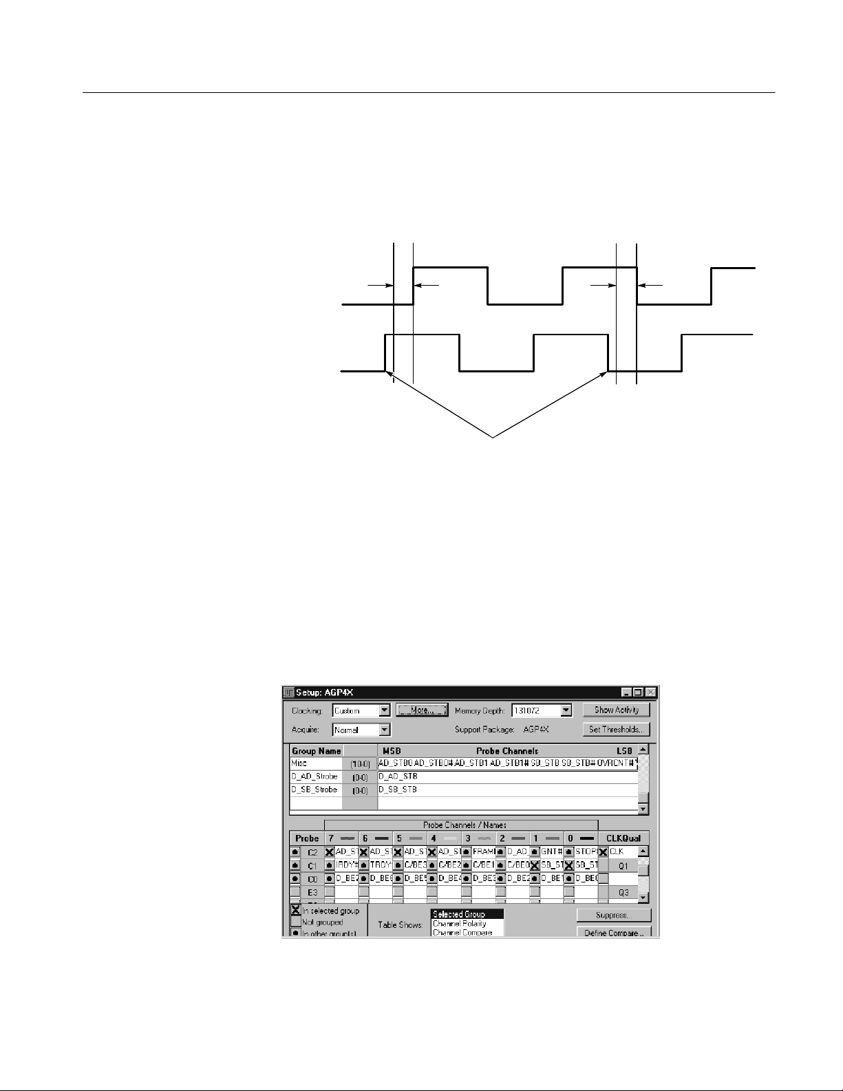
In Figure 2--1, the D_AD_STB signal has sufficient Setup/Hold time with respect
to the CLK edge. In this case, no adjustment is required.
2.5 ns
CLK
D_AD_STB
Signal change occurs greater than 2.5 ns
before a rising or falling CLK edge
2.5 ns
Figure 2--1: Examples of sufficient setup/hold times
Consider the next case:
In Figure 2--4, the D_AD_STB signal is changing within 2.5 ns of the CLK edge.
You will need to modify the default Setup/Hold values by following these steps:
1. In the System window, click Setup. In the Setup:AGP4X window, click More
(see Figure 2--2).
Figure 2--2: Setup:AGP4X window
TMS808 AGP4X Bus State Support
2--9
Page 58

Setting Up the Support
2. In the Custom Options window, under the Setup/Hold Window, scroll down
and click on the Support Package Default heading for D_AD_Strobe.
3. Select --500 ps/2.5 ns. Click OK (see Figure 2--3).
Figure 2--3: Custom option window
In this case, the Setup/Hold value is --0.5 ns Setup/2.5ns Hold. Each case may
require different values. Be sure to select Setup/Hold values that are not violated
by D_AD_STB.
2.5 ns
CLK
D_AD_STB
2.5 ns
Signal change occurs within
2.5 ns of rising CLK edge
Signal change occurs within
2.5 ns of falling CLK edge
Figure 2--4: Setup/hold time violation examples
Once the Setup/Hold values for the D_AD_STB signal (that is, the
D_AD_Strobe group) are determined, the same values must be entered in the
AGP_Data_Hi, AGP_Data_Lo, BE_Hi and BE_Lo groups.
2--10
TMS808 AGP4X Bus State Support
Page 59

Setting Up the Support
NOTE. Since the AD_STB timings with respect to CLK can be different for READs
and WRITEs, the Setup/Hold time should satisfy the condition in both cases so
that data can be accurately logged for AGP READs and AGP WRITEs.
Similarly, the Setup/Hold values for the D_SB_STB signal (that is, D_SB_Strobe
group) are determined and the same values are to be entered in the SBA_Hi and
SBA_Lo groups.
Signals Not On the Probe
Adapter
Extra Channels
The TMS 808 probe adapter provides access for all of the AGP4X signals.
The following channels on the logic analyzer are left free for you to connect to
other signals of interest:
H Hi_E3:7-0 (for 136 channel module only)
H Hi_E2:7-0 (for 136 channel module only)
H Hi_E1:7-0 (for 136 channel module only)
H Hi_E0:7-0 (for 136 channel module only)
H Hi_C3:7-0
H Hi_C1:7-0
H Hi_C0:7-0
H Hi_A1:1-0
TMS808 AGP4X Bus State Support
2--11
Page 60

Setting Up the Support
2--12
TMS808 AGP4X Bus State Support
Page 61

Specifications
Page 62

Page 63

Specifications
Circuit Description
This chapter contains information regarding the specifications of the support.
AGP4X support uses two distinctive types of transactions on the same physical
bus, depending on which of the signals the transaction is synchronized to. The
first set is synchronized to the 66 MHz AGP clock, and the second set is
synchronized to the strobe signals. The timing relationship of the Strobe signals
to the Clock is described in detail in the Accelerated Graphics Port Interface
Specification, Intel, Version 2.0, 1998.
The AGP bus is a point to point bus and its behavior with an added third load is
not specifified. If a third load (like the probe adapter) is added, it is the responsibility of the user to ensure that the system meets the AGP Interface specifications. The loading information and equivalent circuits for the probe adapter is
provided on page 3--6. The critical timing constraints are mainly in the form of
skew budget, which are separately allocated for the motherboard and the AGP4X
connector.
The interface point between the motherboard and the AGP4X connector comes
on the transmission line of the signals. So when probing the signals at the
connector, you will encounter a composite signal made of the ongoing transmission and the reflection from the receiving end, as the AGP bus is source
terminated. As the signaling period reduces and approaches the transit time over
the bus length, it becomes very difficult to extract valid data from the composite
waveform. In the case of TMS 808 support, circuitry on the extender board
performs the task of extracting digital signals from the composite wave present
on the bus.
Once the digital signals are extracted, the transactions need to be captured by the
Logic Analyzer. The two issues involved are a high data rate (266 MHz), that is
more than the logic analyzer module can handle and two types of synchronization, as mentioned previously.
The first issue, high data rate, is handled by demultiplexing the data, reducing the
rate to 133 MHz. At this rate, the logic analyzer is able to directly acquire the
data presented. The respective Strobe signals are used to latch data in latches, and
both edges of the AGP clock are used to log these latched outputs.
The second issue, two types of synchronization, are shown in the block diagram
of the logic circuit, which implements demultiplexing the data (see Figure 3--1).
TMS808 AGP4X Bus State Support
3--1
Page 64

Specifications
AD [31--0]
AD_STB0
RST~
AD_STB0#
AD [31--0]
Figure 3--1: Block diagram for AD bus
The first data value on the 32-bit bus is latched into latch D1 by the falling edge
of AD_STB0. In fact, the lower significant 16 bits uses AD_STB0 and the upper
significant 16 bits uses AD_STB1, but for simplicity, the block diagram shows
only a single 32 bit latch. The falling edge of the complementary strobe
AD_STB0# latches the second data in D2, at the same time moving the data at
the output of D1 into another latch D3. This is done to avoid the D1 data being
overwritten by the next edge of the AD_STB0. More than three strobe edges
cannot be accommodated in one half cycle of AGP clock, so the TLA always
gets a chance to acquire the data before it gets overwritten. When lower speed
(1X, PCI for example) cycles are being run, TLA picks up the AD bus information directly from the bus rather than from the latched output. On the user
interface, the latched AD bus data appears as AGP_Data_Hi and AGP_Data_Lo.
D1
D2
CLK
CLK
MR
MR
Q1
Q2
D3
CLK
32 bits
MR
Q3
32 bits32 bits
To TL A
64 bits
3--2
The same principle is applied on the side band signals, using another set of
latches (see Figure 3--2).
TMS808 AGP4X Bus State Support
Page 65

Specifications
SBA [7--0]
SB_STB
RST~
SB_STB#
SBA [7--0]
Figure 3--2: Block diagram for the SBA bus
The 32-bit AD bus splits into a 64-bit bus at the logic analyzer input, and the
8-bit SBA bus splits into 16 bits. After this, latched data is valid up to 7.5 ns, in
most cases it will provide the necessary setup time for the logic analyzer, even if
the AGP clock is used for logging in data. In rare instances, the clock-edge-tostrobe timing may have a setup/hold violation in the logic analyzer. In this case,
the adjustable Setup/Hold values of the logic analyzer can be used to make
accurate data acquisitions.
D1 Q1
CLK
D2
CLK
MR
Q2
MR
D3 Q3
CLK
MR
8 bits
8 bits8 bits
To TL A
16 bits
For the logic analyzer to detect the availability of fresh data, a qualifier is
required that can be reliably acquired at the same acquisition speed. Since no
signal from the AGP bus can be used for this purpose, two signals are derived
from the strobe. A single-toggle flip-flop is used to generate the common
qualifier D_AD_STB. Data is always logged in as 64 bits into the logic analyzer.
Only when the second set of data arrives on the falling edge of the AD_STB0#,
is the data logged in as 64 bits. Also, the support makes use of the fact that there
are always 4 falling edges occurring in the AGP4x; irrespective, of whether the
data is valid or not. Similarly another qualifier is derived for the SBA signals (see
Figure 3--3).
TMS808 AGP4X Bus State Support
3--3
Page 66

Specifications
TQ
AD_ STB0#
MR
RST~
D_AD_STB
Figure 3--3: Qualifier generation
The AGP 2X support included with this package operates in a similar manner.
The only difference is that the derived qualifiers get replaced by the corresponding strobe signals themselves.
The support masters all signals in all three cases; when an AGP transfer is on the
AD bus, there is activity on the side band strobes, and the system is running PCI
cycles. This means, except for the bus whose activity caused the master point,
other buses may have invalid data. The disassembler locates such invalid data on
the various buses and marks them as invalid with dashes. In the SBA mode, the
side band strobe is active even when there is no data to be passed. So, if the data
being queued is NOPs, and there is no valid data on any other buses, such
samples are suppressed by the disassembler.
Specifications
3--4
These specifications are for a probe adapter connected between a compatible
Tektronix logic analyzer and a System Under Test (SUT). Table 3--1 shows the
electrical requirements the SUT must produce for the support to acquire correct
data.
Table 3--1: Electrical specifications
Characteristics Requirements
SUT DC power requirements The support uses an external power
supply and does not draw any current
from the SUT.
Probe adapter: DC power requirements
Voltage, VCC 4.75 -- 5.25 VDC
Current, VCC I
typical
4.0 A
TMS808 AGP4X Bus State Support
Page 67

Specifications
Table 3--1: Electrical specifications (cont.)
Characteristics Requirements
I
maximum
AC adapter
Input Voltage rating 90 -- 265 V CAT II
Input Frequency Rating 47 -- 63 Hz
Output Voltage Rating 5 V
Output Current Rating 8 A
Output Power Rating 40 W
SUT clock rate Maximum 66 MHz
Set up and hold time requirements SUT should meet AGP 2.0
specifications
Note; All Reserved pins are connected through the probe adapter. All VCC3.3 pins are shorted
together on the probe adapter. All Vddq3.3 pins are shorted together on the probe adapter. All
5.0 V pins are shorted together on the probe adapter.
4.2 A
Table 3--2 shows the environmental specifications.
Table 3--2: Environmental specifications
Characteristic Description
Temperature
Maximum operating +50 °C (+122 °F)
Minimum operating 0 °C (+32 °F)
Non operating -- 5 5 °Cto+75°C(--67° to +167 °F)
Humidity 10 to 95% relative humidity
Altitude
Operating 4.5 km (15,000 ft) maximum
Non operating 15 km (50,000 ft) maximum
Electrostatic immunity The probe adapter is static sensitive
1
Designed to meet Tektronix standard 062-2847-00 class 5.
2
Not to exceed AGP4X bus thermal considerations. Forced air cooling might be
required.
1
2
TMS808 AGP4X Bus State Support
3--5
Page 68

Specifications
Loading and Equivalent Circuits
The load presented to the SUT by the AGP probe adapter is low. The following
approximation of the probe adapter loading is sufficient for most circuit-simulation calculations.
Table 3--3 shows the values you can use to calculate characteristics of the lossy
delay lines shown in Figure 3--4 on page 3--7.
Table 3--3: Lossy delay line values
Characteristic Value
C (capacitance) 3 pF per inch
L (inductance) 10.8 nH per inch
R (resistance)
Z0(impedance)
.067 Ω per inch
60 Ω
3--6
TMS808 AGP4X Bus State Support
Page 69

Mother
board
5pF
Specifications
1 H
1ns60Ω
AGP board
1pF
3 Ω
High-speed conditioned lines
Mother
board
1pF
10 KΩ
1ns60Ω
FRAME#, STOP#, GNT#, IRDY#, TRDY#,
RST#, PME#, INTA#, and INTB# lines
Mother
board
1pF
10 pF
20 KΩ
1ns60Ω
10 KΩ
CLK line
Figure 3--4: Equivalent circuit loads for the probe adapter
AGP board
1pF
AGP board
1pF
Figure 3--5 shows the dimensions of the probe adapter.
TMS808 AGP4X Bus State Support
3--7
Page 70
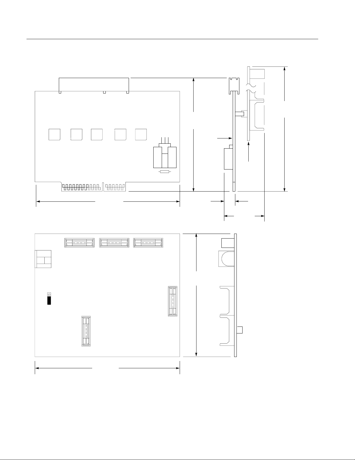
Specifications
Graphics card extender
185.42 mm
(7.730 in)
120.65 mm
(4.750 in)
Graphics
card
extender
board
Probe
interface
board
Probe interface board
152.40 mm
(6.000 in)
153.03 mm
(6.025 in)
13.97 mm
(0.550 in)
44.45 mm
(1.750 in)
129.54 mm
(5.100 in)
Figure 3--5: Probe adapter dimensions
3--8
TMS808 AGP4X Bus State Support
Page 71

Diagrams
Page 72

Page 73

Diagrams and Circuit Board Illustrations
This section contains the troubleshooting procedures, block diagrams, circuit board illustrations,
component locator tables, waveform illustrations, and schematic diagrams.
Graphic Items and Special Symbols Used in This Manual
Each assembly in the instrument is assigned an assembly number (for example A5). The
assembly number appears in the title on the diagram, in the lookup table for the schematic
diagram, and corresponding component locator illustration. The Replaceable Electrical Parts
list is arranged by assembly in numerical sequence; the components are listed by component
number.
Symbols
Graphic symbols and class designation letters are based on ANSI Standard Y32.2-1975.
Abbreviations are based on ANSI Y1.1-1972.
Logic symbology is based on ANSI/IEEE Standard 91-1984 in terms of positive logic. Logic
symbols depict the logic function performed and can differ from the manufacturer’s data.
The tilde (~) preceding a signal name indicates that the signal performs its intended function
when in the low state.
Other standards used in the preparation of diagrams by Tektronix, Inc., include the following:
H Tektronix Standard 062-2476 Symbols and Practices for Schematic Drafting
H ANSI Y14.159-1971 Interconnection Diagrams
H ANSI Y32.16-1975 Reference Designations for Electronic Equipment
H MIL-HDBK-63038-1A Military Standard Technical Manual Writing Handbook
Locator Grid
Function Block Title
Internal Screw Adjustment
Onboard Jumper
Digital Ground
Refer to Assembly
& Diagram Number
Offboard Connector
Active Low Signal
Signal From
Another Diagram,
Same Board
A
B
12 3
Component Locator Diagrams
The schematic diagram and circuit board component location illustrations have grids marked
on them. The component lookup tables refer to these grids to help you locate a component.
The circuit board illustration appears only once; its lookup table lists the diagram number of
all diagrams on which the circuitry appears.
Some of the circuit board component location illustrations are expanded and divided into
several parts to make it easier for you to locate small components. To determine which part
of the whole locator diagram you are looking at, refer to the small locator key shown below.
The gray block, within the larger circuit board outline, shows where that part fits in the
whole locator diagram. Each part in the key is labeled with an identifying letter that appears
in the figure titles under component locator diagrams.
4
SYNC GENERATOR A5
SYNC BOARD
Power Termination
Component on back of board
Strap
Panel Control
Female Coaxial
Connector
Heat Sink
Decoupled Voltage
Diagram Number
Assembly Number
Diagram Name
Component Values
Electrical components shown on the diagrams are in the following units unless noted
otherwise:
Capacitors: Values one or greater are in picofarads (pF).
Resistors: Values are in Ohms (Ω).
TMS 808 AGP4X Bus State Support
Values less than one are in microfarads (F).
Section of Circuit
Board Shown
A B
DC
4- 1
Page 74

TMS 808 Probe graphics card extender (Front) TMS 808 Probe graphics card extender (Back)
4- 2
TMS 808 AGP4X Bus State Support
Page 75
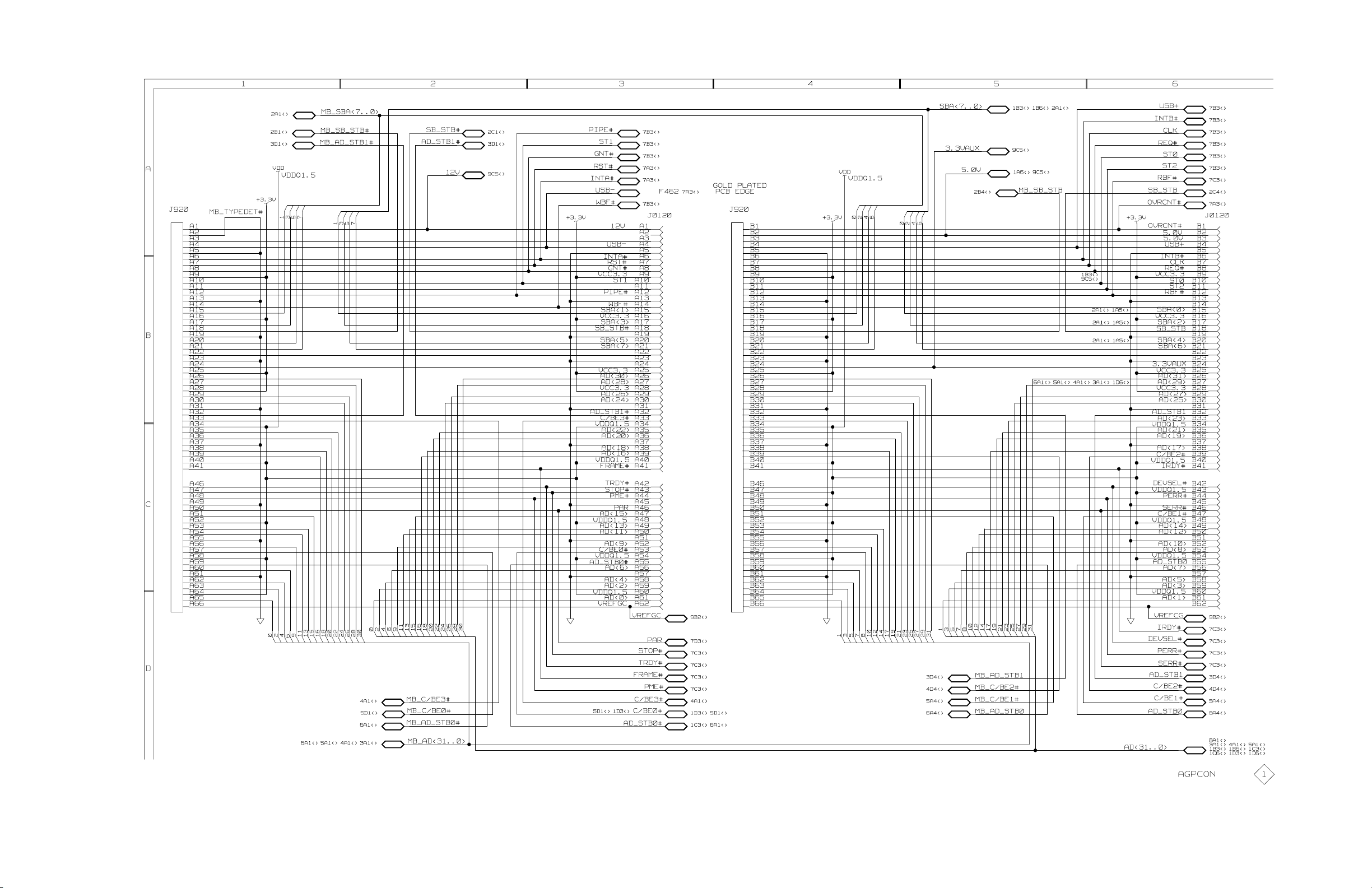
TMS 808 AGP4X Bus State Support
4--3
Page 76

4--4
TMS 808 AGP4X Bus State Support
Page 77

TMS 808 AGP4X Bus State Support
4--5
Page 78

4--6
TMS 808 AGP4X Bus State Support
Page 79

TMS 808 AGP4X Bus State Support
4--7
Page 80

4--8
TMS 808 AGP4X Bus State Support
Page 81

TMS 808 AGP4X Bus State Support
4--9
Page 82

4--10
TMS 808 AGP4X Bus State Support
Page 83

TMS 808 AGP4X Bus State Support
4--11
Page 84

4--12
TMS 808 AGP4X Bus State Support
Page 85

TMS 808 AGP4X Bus State Support
4--13
Page 86

4--14
TMS 808 AGP4X Bus State Support
Page 87

TMS 808 AGP4X Bus State Support
4--15
Page 88

4--16
TMS 808 AGP4X Bus State Support
Page 89

TMS 808 AGP4X Bus State Support
4--17
Page 90

4--18
TMS 808 AGP4X Bus State Support
Page 91

TMS 808 AGP4X Bus State Support
4--19
Page 92

4--20
TMS 808 AGP4X Bus State Support
Page 93

TMS 808 AGP4X Bus State Support
4--21
Page 94

4--22
TMS 808 AGP4X Bus State Support
Page 95

TMS 808 AGP4X Bus State Support
4--23
Page 96

R210
R220
FD2
J0140 J0120J0160
R232R230
R241
R242
R250
R260
R263
R271
R280
R0281
R0270
R0262
R0261
R0251
R0243
R0240
R0233
R0231
R0211R0221
MH1
MH2
FD3
Q810
Q811
C510
R411
Q610
U610
U810
U310
U511
R421
C920
C921
C922
Q620
Q621
Q720Q710
R721
C931
C932
R431
R833
R930
U330
U531
R834
R731
C930
C933
R835
R434
R732
R931
R836
J0290
R0680
R0380
R0381
R0481
R0472
R0471
R0462
C954
R951
R452
R855
U360
R461 R480
U561
U340
R441
R451
U541
R640
R751
R742 R750R730
R741R740
J740
R850
C942
C950
R852
C952
R950
R851R842R841
R853
R854
C951
C953
R840R832R831R830
C840
R843
R844
C940
R940
R941
R943
R470
U370
U571
MH3
MH4
U580
F390
C490
J0590
FD1
R0350
R0351
R0453
TP2
TP1
U0951 U0920
U0953
R0442R0460
U0540 U0530
R0944
R0440
R0540
R0942
R0340
R0341
R0530
R0320
U0921
R0621
R0622
R0623
R0720
R0420
R0430
R0432
R0433R0450
U0930U0940
U0931U0950
U0933U0952
U0932
R0612
C0710
U0510U0560U0570
R0817
C0810
R0410
R0812
R0813
R0814
R0815
4--24
TMS 808 A1 Probe interface board (Front) TMS 808 A1 Probe interface board (Back)
TMS 808 AGP4X Bus State Support
Page 97

TMS 808 AGP4X Bus State Support
4--25
Page 98

4--26
TMS 808 AGP4X Bus State Support
Page 99

TMS 808 AGP4X Bus State Support
4--27
Page 100

4--28
TMS 808 AGP4X Bus State Support
 Loading...