

Page 1

Instruction Manual
TMS711
320C6211/C6711 Microprocessor Support
071-0877-00
Warning
The servicing instructions are for use by qualified
personnel only. To avoid personal injury, do not
perform any servicing unless you are qualified to
do so. Refer to all safety summaries prior to
performing service.
www.tektronix.com
Page 2

Copyright © T ektronix, Inc. All rights reserved. Licensed software products are owned by Tektronix or its suppliers and
are protected by United States copyright laws and international treaty provisions.
Use, duplication, or disclosure by the Government is subject to restrictions as set forth in subparagraph (c)(1)(ii) of the
Rights in T echnical Data and Computer Software clause at DFARS 252.227-7013, or subparagraphs (c)(1) and (2) of the
Commercial Computer Software – Restricted Rights clause at F AR 52.227-19, as applicable.
T ektronix products are covered by U.S. and foreign patents, issued and pending. Information in this publication supercedes
that in all previously published material. Specifications and price change privileges reserved.
T ektronix, Inc., P.O. Box 500, Beaverton, OR 97077
TEKTRONIX and TEK are registered trademarks of T ektronix, Inc.
Page 3

SOFTWARE WARRANTY
T ektronix warrants that the media on which this software product is furnished and the encoding of the programs on
the media will be free from defects in materials and workmanship for a period of three (3) months from the date of
shipment. If a medium or encoding proves defective during the warranty period, T ektronix will provide a
replacement in exchange for the defective medium. Except as to the media on which this software product is
furnished, this software product is provided “as is” without warranty of any kind, either express or implied.
T ektronix does not warrant that the functions contained in this software product will meet Customer’s
requirements or that the operation of the programs will be uninterrupted or error-free.
In order to obtain service under this warranty, Customer must notify Tektronix of the defect before the expiration
of the warranty period. If T ektronix is unable to provide a replacement that is free from defects in materials and
workmanship within a reasonable time thereafter, Customer may terminate the license for this software product
and return this software product and any associated materials for credit or refund.
THIS WARRANTY IS GIVEN BY TEKTRONIX IN LIEU OF ANY OTHER WARRANTIES, EXPRESS
OR IMPLIED. TEKTRONIX AND ITS VENDORS DISCLAIM ANY IMPLIED WARRANTIES OF
MERCHANTABILITY OR FITNESS FOR A PARTICULAR PURPOSE. TEKTRONIX’
RESPONSIBILITY TO REPLACE DEFECTIVE MEDIA OR REFUND CUSTOMER’S PAYMENT IS
THE SOLE AND EXCLUSIVE REMEDY PROVIDED TO THE CUSTOMER FOR BREACH OF THIS
WARRANTY. TEKTRONIX AND ITS VENDORS WILL NOT BE LIABLE FOR ANY INDIRECT,
SPECIAL, INCIDENTAL, OR CONSEQUENTIAL DAMAGES IRRESPECTIVE OF WHETHER
TEKTRONIX OR THE VENDOR HAS ADVANCE NOTICE OF THE POSSIBILITY OF SUCH
DAMAGES.
Page 4

Page 5

Table of Contents
Getting Started
Operating Basics
General Safety Summary v. . . . . . . . . . . . . . . . . . . . . . . . . . . . . . . . . . . .
Preface ix. . . . . . . . . . . . . . . . . . . . . . . . . . . . . . . . . . . . . . . . . . . . . . . . . . .
Manual Conventions ix. . . . . . . . . . . . . . . . . . . . . . . . . . . . . . . . . . . . . . . . . . . . . .
Contacting T ektronix x. . . . . . . . . . . . . . . . . . . . . . . . . . . . . . . . . . . . . . . . . . . . . .
Support Package Description 1–1. . . . . . . . . . . . . . . . . . . . . . . . . . . . . . . . . . . . . . . .
Logic Analyzer Software Compatibility 1–1. . . . . . . . . . . . . . . . . . . . . . . . . . . . . . .
Logic Analyzer Configuration 1–2. . . . . . . . . . . . . . . . . . . . . . . . . . . . . . . . . . . . . . .
Requirements and Restrictions 1–2. . . . . . . . . . . . . . . . . . . . . . . . . . . . . . . . . . . . . . .
Functionality Not Supported 1–4. . . . . . . . . . . . . . . . . . . . . . . . . . . . . . . . . . . . . . . .
Features not T ested 1–4. . . . . . . . . . . . . . . . . . . . . . . . . . . . . . . . . . . . . . . . . . . . . . . .
Miscellaneous 1–4. . . . . . . . . . . . . . . . . . . . . . . . . . . . . . . . . . . . . . . . . . . . . . . . . . . .
Connecting the Logic Analyzer to a System Under T est 1–5. . . . . . . . . . . . . . . . . . .
Setting Up the Support 2–1. . . . . . . . . . . . . . . . . . . . . . . . . . . . . . . . . . . . . .
Installing the Support Software 2–1. . . . . . . . . . . . . . . . . . . . . . . . . . . . . . . . . . . . . .
Channel Group Definitions 2–1. . . . . . . . . . . . . . . . . . . . . . . . . . . . . . . . . . . . . . . . .
Support Package Setups 2–2. . . . . . . . . . . . . . . . . . . . . . . . . . . . . . . . . . . . . . . . . . . .
Clocking 2–2. . . . . . . . . . . . . . . . . . . . . . . . . . . . . . . . . . . . . . . . . . . . . . . . . . . . . . . .
Acquiring and Viewing Disassembled Data 2–13. . . . . . . . . . . . . . . . . . . . .
Acquiring Data 2–13. . . . . . . . . . . . . . . . . . . . . . . . . . . . . . . . . . . . . . . . . . . . . . . . . . .
Viewing Disassembled Data 2–13. . . . . . . . . . . . . . . . . . . . . . . . . . . . . . . . . . . . . . . .
Timing Display Format 2–14. . . . . . . . . . . . . . . . . . . . . . . . . . . . . . . . . . . . . . . . .
Hardware Display Format 2–14. . . . . . . . . . . . . . . . . . . . . . . . . . . . . . . . . . . . . . .
Software Display Format 2–15. . . . . . . . . . . . . . . . . . . . . . . . . . . . . . . . . . . . . . .
Control Flow Display Format 2–15. . . . . . . . . . . . . . . . . . . . . . . . . . . . . . . . . . . .
Subroutine Display Format 2–15. . . . . . . . . . . . . . . . . . . . . . . . . . . . . . . . . . . . . .
Changing How Data is Displayed 2–16. . . . . . . . . . . . . . . . . . . . . . . . . . . . . . . . . . . .
Optional Display Selections 2–16. . . . . . . . . . . . . . . . . . . . . . . . . . . . . . . . . . . . .
Micro Specific Fields 2–16. . . . . . . . . . . . . . . . . . . . . . . . . . . . . . . . . . . . . . . . . .
Marking Cycles 2–21. . . . . . . . . . . . . . . . . . . . . . . . . . . . . . . . . . . . . . . . . . . . . . .
Viewing an Example of Disassembled Data 2–21. . . . . . . . . . . . . . . . . . . . . . . . . . . .
Specifications
Replaceable Parts
Index
TMS711 320C6211/C6711 Microprocessor Support
i
Page 6

Table of Contents
List of Figures
Figure 2–1: Bus timing for the SBSRAM Read cycle with a burst of four
data transitions 2–4. . . . . . . . . . . . . . . . . . . . . . . . . . . . . . . . . . . . . . . . .
Figure 2–2: SDSRAM Write cycles with a burst of four data
transitions 2–6. . . . . . . . . . . . . . . . . . . . . . . . . . . . . . . . . . . . . . . . . . . . .
Figure 2–3: Bus timing for the ASYNC read cycle 2–7. . . . . . . . . . . . . . .
Figure 2–4: Bus timing for the ASYNC write cycle 2–8. . . . . . . . . . . . . . .
Figure 2–5: Bus timing for the SDRAM fetch cycle with
CAS latency of 3 2–9. . . . . . . . . . . . . . . . . . . . . . . . . . . . . . . . . . . . . . . .
Figure 2–6: SDRAM Write cycle with default of four data transitions 2–11
Figure 2–7: Hardware display format 2–15. . . . . . . . . . . . . . . . . . . . . . . . . .
Figure 2–8: 2–22. . . . . . . . . . . . . . . . . . . . . . . . . . . . . . . . . . . . . . . . . . . . . . .
Figure 5–1: Pin assignments for a Mictor connector
(component side) 5–7. . . . . . . . . . . . . . . . . . . . . . . . . . . . . . . . . . . . . . . .
ii
TMS711 320C6211/C6711 Microprocessor Support
Page 7

List of Tables
Table of Contents
Table 2–1: Signal acquisition in SBSRAM Read cycle 2–4. . . . . . . . . . . .
Table 2–2: Signal acquisition in SBSRAM Write cycle 2–6. . . . . . . . . . .
Table 2–3: Signal acquisition in ASYNC Write cycle 2–8. . . . . . . . . . . . .
Table 2–4: Signal acquisition in ASYNC Write cycle 2–9. . . . . . . . . . . . .
Table 2–5: Signal acquisition in SDRAM fetch cycle with
CAS latency of 3 2–10. . . . . . . . . . . . . . . . . . . . . . . . . . . . . . . . . . . . . . . .
Table 2–6: Signal acquisiton in SDRAM write cycle with
CAS latency of 3 2–12. . . . . . . . . . . . . . . . . . . . . . . . . . . . . . . . . . . . . . . .
Table 2–7: Description of special characters in the display 2–13. . . . . . . .
Table 2–8: Cycle type definitions 2–14. . . . . . . . . . . . . . . . . . . . . . . . . . . . .
Table 2–9: C6211/C6711 Compatible SDRAM Memory
Configuration 2–18. . . . . . . . . . . . . . . . . . . . . . . . . . . . . . . . . . . . . . . . .
Table 3–1: C6211 Electrical specifications 3–1. . . . . . . . . . . . . . . . . . . . .
Table 3–2: C6711 Electrical Specifications 3–2. . . . . . . . . . . . . . . . . . . . .
Table 5–1: Control symbol table definitions 5–1. . . . . . . . . . . . . . . . . . . .
Table 5–2: Address channel group assignments 5–3. . . . . . . . . . . . . . . . .
Table 5–3: Data channel group assignments 5–3. . . . . . . . . . . . . . . . . . . .
Table 5–4: Control channel group assignments 5–5. . . . . . . . . . . . . . . . . .
Table 5–5: Async channel group assignments 5–5. . . . . . . . . . . . . . . . . . .
Table 5–6: CEnable channel group assignments 5–5. . . . . . . . . . . . . . . . .
Table 5–7: BEnable channel group assignments 5–5. . . . . . . . . . . . . . . . .
Table 5–8: Misc channel group assignments 5–6. . . . . . . . . . . . . . . . . . . .
Table 5–9: Clock and Qualifier channel assignments 5–6. . . . . . . . . . . . .
Table 5–10: CPU to Mictor connections for Mictor A pins 5–7. . . . . . . .
Table 5–11: CPU to Mictor connections for Mictor D pins 5–9. . . . . . . .
Table 5–12: CPU to Mictor connections for Mictor C pins 5–10. . . . . . . .
Table 5–13: CPU to Mictor connections for CEnable 5–10. . . . . . . . . . . . .
Table 5–14: CPU to Mictor connections for BEnable 5–10. . . . . . . . . . . . .
Table 5–15: CPU to Mictor connections for Misc 5–11. . . . . . . . . . . . . . . .
Table 5–16: CPU to Mictor connections for clock and qualifiers 5–11. . .
TMS711 320C6211/C6711 Microprocessor Support
iii
Page 8

Table of Contents
iv
TMS711 320C6211/C6711 Microprocessor Support
Page 9

General Safety Summary
Review the following safety precautions to avoid injury and prevent damage to
this product or any products connected to it. To avoid potential hazards, use this
product only as specified.
Only qualified personnel should perform service procedures.
While using this product, you may need to access other parts of the system. Read
the General Safety Summary in other system manuals for warnings and cautions
related to operating the system.
To Avoid Fire or Personal Injury
Connect and Disconnect Properly . Do not connect or disconnect probes or test
leads while they are connected to a voltage source.
Ground the Product. This product is indirectly grounded through the grounding
conductor of the mainframe power cord. To avoid electric shock, the grounding
conductor must be connected to earth ground. Before making connections to the
input or output terminals of the product, ensure that the product is properly
grounded.
Observe All Terminal Ratings. To avoid fire or shock hazard, observe all ratings
and marking on the product. Consult the product manual for further ratings
information before making connections to the product.
The common terminal is at ground potential. Do not connect the common
terminal to elevated voltages.
Do Not Operate Without Covers. Do not operate this product with covers or panels
removed.
Avoid Exposed Circuitry. Do not touch exposed connections and components
when power is present.
Do Not Operate in Wet/Damp Conditions.
Do Not Operate in an Explosive Atmosphere.
Keep Product Surfaces Clean and Dry .
TMS711 320C6211/C6711 Microprocessor Support
v
Page 10

General Safety Summary
Symbols and Terms
T erms in this Manual. These terms may appear in this manual:
WARNING. Warning statements identify conditions or practices that could result
in injury or loss of life.
CAUTION. Caution statements identify conditions or practices that could result in
damage to this product or other property.
T erms on the Product. These terms may appear on the product:
DANGER indicates an injury hazard immediately accessible as you read the
marking.
WARNING indicates an injury hazard not immediately accessible as you read the
marking.
CAUTION indicates a hazard to property including the product.
Symbols on the Product. The following symbols may appear on the product:
WARNING
High Voltage
Protective Ground
(Earth) T erminal
CAUTION
Refer to Manual
Double
Insulated
vi
TMS711 320C6211/C6711 Microprocessor Support
Page 11

Preface
Manual Conventions
This instruction manual contains specific information about the TMS711
320C6211/C6711 microprocessor support package and is part of a set of
information on how to operate this product on compatible Tektronix logic
analyzers.
If you are familiar with operating microprocessor support packages on the logic
analyzer for which the TMS711 320C6211/C6711 support was purchased, you
will only need this instruction manual to set up and run the support.
If you are not familiar with operating microprocessor support packages, you will
need to supplement this instruction manual with information on basic operations
to set up and run the support. See Manual Conventions below for more information.
This manual uses the following conventions:
H The term “disassembler” refers to the software that disassembles bus cycles
into instruction mnemonics and cycle types.
H The phrase “information on basic operations” refers to online help, an
installation manual, or a user manual covering the basic operations of
microprocessor support.
TMS711 320C6211/C6711 Microprocessor Support
vii
Page 12

Preface
Contacting Tektronix
Phone 1-800-833-9200*
Address Tektronix, Inc.
Department or name (if known)
14200 SW Karl Braun Drive
P.O. Box 500
Beaverton, OR 97077
USA
Web site www.tektronix.com
Sales support 1-800-833-9200, select option 1*
Service support 1-800-833-9200, select option 2*
Technical support Email: techsupport@tektronix.com
1-800-833-9200, select option 3*
1-503-627-2400
6:00 a.m. – 5:00 p.m. Pacific time
* This phone number is toll free in North America. After office hours, please leave a
voice mail message.
Outside North America, contact a Tektronix sales office or distributor; see the
Tektronix web site for a list of offices.
viii
TMS711 320C6211/C6711 Microprocessor Support
Page 13

Getting Started
Page 14

Page 15

Getting Started
This chapter contains information on the TMS711 320C6211/C6711 microprocessor support package, and information on connecting your logic analyzer to
your system under test.
Support Package Description
The TMS711 320C6211/C6711microprocessor support package displays
disassembled data from systems based on the Texas Instruments C6211/C6711
microprocessor.
To use this support efficiently, you need to have the items listed in the information on basic operations and the following documents:
H TMS320C6000 CPU and Instruction Set Reference Guide, Literature
Number: SPRU189D, March 1999.
H TMS320C6000 Peripheral Reference Guide, Literature Number: SPRU190C,
April 1999.
H TMS320C6000 EMIF to External SDRAM/SGRAM Interface, Literature
Number: SPRA433A, June 1999.
H TMS320C6000 EMIF to External SBSRAM Interface, Literature Number:
SPRA533A, April 1999.
H TMS320C6000 Digital Signal Processor Data Sheet, Literature Number:
SPRS073, March 1999.
H TMS320C6000 EMIF to External Asynchronous SRAM Interface, Literature
Number: SPRA542, April 1999.
Information on basic operations also contains a general description of support.
Logic Analyzer Software Compatibility
The floppy disk label on the microprocessor support states which version of logic
analyzer software this support is compatible with.
TMS711 320C6211/C6711 Microprocessor Support
1–1
Page 16

Getting Started
Logic Analyzer Configuration
The TMS711 320C6211/C6711support requires a minimum of one 102-channel
module.
NOTE. It is recommended that a logic analyzer acquisition module with a
maximum bus speed of 100 MHz be required when ECLKOUT = 100 MHz
(maximum). For ECLKOUT above 100 MHz (maximum), a logic analyzer
acquisition module with a maximum bus speed of 200 MHz is required.
Requirements and Restrictions
You should review the general requirements and restrictions of microprocessor
support packages in the information on basic operations as they pertain to your
system under test.
System Clock Rate
NonIntrusive Acquisition
Disabling the Instruction
Cache
L2 Cache
You should also review electrical, environmental, and mechanical specifications
in Specifications on page 3–1 as they pertain to your system under test, as well as
the following descriptions of other C6211/C6711 support requirements and
restrictions.
The operating speeds that the C6211/C6711
C6211/C6711 microprocessor are listed on Table 3–1. These specification were
valid at the time this manual was printed. Please contact your Tektronix Sales
Representative for current information on the fastest devices supported.
Acquiring microprocessor bus cycles will be non intrusive to the system under
test. That is, the C6211/C6711 support will not intercept, modify, or present
signals back to the system under test.
To display disassembled acquired data, you must disable the internal instruction
cache. Disabling the cache makes all instruction prefetches visible on the bus
they then can be acquired and displayed disassembled.
Do not configure L2 cache as cache; or external memory bus cycle acquisitions
will not occur with L2 cache.
support can acquire data from the
1–2
Write Cycle
SBSRAM Write Cycle and SDRAM Write Cycle have the same control values,
so they are represented by a single name. For example SDWRITE/SBSWRITE
for a given sequence in the control column, but the corresponding mnemonic
TMS711 320C6211/C6711 Microprocessor Support
Page 17

Getting Started
column will have clear cut labels, for example ( SDRAM WRITE CYCLE ) and
( SBSRAM WRITE CYCLE ).
Read Cycle
Opcode Fetch/Data Read.
Symbol 11111[bin]
Conditional Branches
SBSRAM Read Cycle and SDRAM Read Cycle have same control values, so
they are represented by a single name. For example SDREAD/SBSREAD for a
given sequence in the control column, but the corresponding mnemonic column
will have clear cut labels, for example ( SDRAM READ CYCLE ) and
( SBSRAM READ CYCLE ).
The C6211/C6711 support does not provide a signal to distinguish between Data
Read and Opcode Fetch. The TMS711 320C6211/C6711 support makes a
reasonable estimate at looking at the address values of a few sequences around
the current sequence or by looking at the processor signal. Yet, in some instances
you may need to use the Mark Opcode function.
The Control symbol table does not have a symbol for 11111[bin], since it can
mean SDRAM Read, Write, or Fetch.
Flushes cannot be shown for conditional branches (where Condition is True)
when the branch instruction is in the first fetch packet, and the target address is in
third and fourth fetch packet from the fetch packet which has Branch instructions
(in either forward or reverse branches).
Alternate Fetch Packet
Branch Instructions
Memory Types
SBSRAM 4
Memory-Space Signals
If a conditional branch instruction is in the fetch packet, and the target address is
in the alternate fetch packet (from the fetch packet which has the branch
instruction; for example 1 to 3 , 2 to 4, or 3 to 5) we do not show flushes, since
fetch packets appear in sequence.
For branch instructions (both conditional and unconditional): B.S2 IRP, B.S2
NRP and B.S2 src2reg, we do not show whether a branch was taken or not in the
listing window of our disassembly. Since we cannot get the contents of the
registers IRP, NRP, Bxx that have the target address.
The C6211/C6711
memory types: SDRAM, SBSRAM, and ASYNC, at a time.
SBSRAM 4 word burst Read and write cycles are supported. But SBSRAM 6
word burst Read and write cycles not supported due to timing considerations.
All Memory space signals CE[3–0]~ must be connected to the logic analyzer.
support disassembles the execution from any one of the
TMS711 320C6211/C6711 Microprocessor Support
1–3
Page 18

Getting Started
External Memory
In the C6211
programs only at addresses in multiples of 0x20; for example, 80000000,
80000020,80000040. Hence, the user input fields for entering the start address of
the Interrupt-Service-Fetch packets must be appropriate.
Functionality Not Supported
Microprocessor
Alternate Bus master
The signals: HPI, MCBSP 0 & 1, and JTAG are not acquired. If you want to view
these signals, you need to find an alternate way to probe them.
Alternative bus master transactions are acquired by the C6211/C6711 support and
are not disassembled.
Features not Tested
The C6211/C6711 support has been tested for C6711 floating point instructions
by editing the refmem. The C6211/C6711 support is not evaluated by acquiring
cycles from a dedicated C6711 evaluation board.
external memory you can download the C6211/C6711 support
Miscellaneous
The C6211/C6711 support disassembles SDRAM, SBSRAM and ASYNC
memory cycles. The C6211/C6711 support is not tested for SBSRAM and
ASYNC cycles. This C6211/C6711 support has been tested only with 32bit
SDRAM cycles.
The C6211/C6711 support has not been tested for Interrupts.
The C6211/C6711 support has not been tested for Big Endian mode.
The Address shown for the SDRAM ACTV cycle is the row address for the
corresponding user input for the SDRAM Address Configuration.
1–4
TMS711 320C6211/C6711 Microprocessor Support
Page 19

Connecting the Logic Analyzer to a System Under Test
You can use channel probes, clock probes, and leadsets with a commercial test
clip (or adapter) to make connections between the logic analyzer and your system
under test.
To connect the probes to C6211/C6711 signals in the system under test using a
test clip, follow these steps:
1. Turn off power to your system under test. It is not necessary to turn off
power to the logic analyzer.
CAUTION. Static discharge can damage the microprocessor, the probes, and the
logic analyzer module. To prevent static damage, handle these components only
in a static-free environment.
Always wear a grounding wrist strap, heel strap, or similar device while
handling the microprocessor.
Getting Started
2. To discharge your stored static electricity, touch the ground connector located
on the back of the logic analyzer. If you are using a test clip, touch any of the
ground pins on the clip to discharge stored static electricity from the test clip.
CAUTION. Failure to place the system under test on a horizontal surface before
connecting the test clip can permanently damage the pins on the microprocessor.
3. Place the system under test on a horizontal static-free surface.
4. Use Tables 5–2 through 5–16 beginning on page 5–3 to connect the channel
probes to C6211/C6711 signal pins on the test clip or in the system under
test.
Use leadsets to connect at least one ground lead from each channel probe and
the ground lead from each clock probe to ground pins on your test clip.
TMS711 320C6211/C6711 Microprocessor Support
1–5
Page 20

Getting Started
1–6
TMS711 320C6211/C6711 Microprocessor Support
Page 21

Operating Basics
Page 22

Page 23

Setting Up the Support
The information in this section is specific to the operations and functions of the
TMS711 320C6211/C6711 microprocessor support on any Tektronix logic
analyzer for which it can be purchased.
Before you acquire and display disassembled data, you need to load the support
and specify setups for clocking and triggering as described in the information on
basic operations. The microprocessor support provides default values for each of
these setups as well as user-definable settings.
Installing the Support Software
NOTE. Before you install any software, it is recommended you verify that the
microprocessor support software is compatible with the logic analyzer software.
To install the TMS711 320C6211/C6711 software on your Tektronix logic
analyzer, follow these steps:
1. Insert the floppy disk in the disk drive.
2. Click the Windows Start button, point to Settings, and click Control Panel.
3. In the Control Panel window, double-click Add/Remove Programs.
4. Follow the instructions on the screen for installing the software from the
To remove or uninstall software, follow the above instructions and select
Uninstall. You must close all windows before you uninstall any software.
Channel Group Definitions
The software automatically defines channel groups for the support. The channel
groups for the TMS711 320C6211/C6711 support are Address, Data, Control,
Async, CEnable, BEnable, and Misc. The channel groups tables begin on page
5–1.
floppy disk.
TMS711 320C6211/C6711 Microprocessor Support
2–1
Page 24

Setting Up the Support
Support Package Setups
The TMS711 320C6211/C6711 software installs C6211 support package setup
file.
Clocking
C6211 Setup
Options
This setup provides disassembly support. All signals are not inverted and
displayed as they appear electrically on the front side bus.
Disassembly channel groups:
Address Data Async CEnable
BEnable Misc
The TMS711 320C6211/C6711support offers a microprocessor-specific clocking
mode for the C6211/C6711 microprocessor. This clocking mode is the default
selection whenever you load the TMS711 320C6211/C6711 support.
Disassembly will not be correct with the Internal or External clocking modes.
Information on basic operations describes in more detail how to use these clock
selections for general purpose analysis.
H Internal clocking is used for timing and is based on the clock generated by a
Tektronix logic analyzer. You can configure the clock rate from 50 ms down
to 4 ns resolution.
H External clocking is used when you configure the clocking of data based on
logical combinations of clocks and qualifiers.
2–2
TMS711 320C6211/C6711 Microprocessor Support
Page 25

Setting Up the Support
Custom Clocking
When Custom is selected, the Custom Clocking Options menu will have the
subtitle C6211
will also be displayed.
The TMS711 320C6211/C6711support has three clock state machines (CSM).
There is one select field with the label Memory Type: that field will contain the
following selections: ASYNC, SBSRAM, and SDRAM.
Memory operation type:
ASYNC Selects CSM for ASYNC (default)
SBSRAM Selects CSM for SBSRAM
SDRAM Selects CSM for SDRAM
CAS Latency . Choose this field for only SDRAM Clocking state machine. There
are two options:
Two Choose for CAS latency two
Three Choose for CAS latency three
Setup and Hold Time. The user can change the Setup and Hold time window of all
the signal groups. The default Setup time is 2.5 ns and the Hold time is 0 ns. The
user defined Setup and Hold will have precedence over any default Setup and
Hold time.
Microprocessor Clocking Support added, and the clocking options
NOTE. The signals present in the Async group are also present in the Control
group. The Setup and Hold values entered for the first one of those groups are
used for all instances of that channel in the other groups.
TMS711 320C6211/C6711 Microprocessor Support
2–3
Page 26

Setting Up the Support
Á
Á
Á
Á
Á
Á
Á
Á
БББББ
Á
Á
Á
Á
Á
Á
Á
Á
Á
Á
Á
Á
Á
Á
Á
Á
БББББ
Á
Á
Á
Á
Á
Á
Á
Á
Á
Á
Á
Á
Á
Á
БББББ
Á
Á
Á
Á
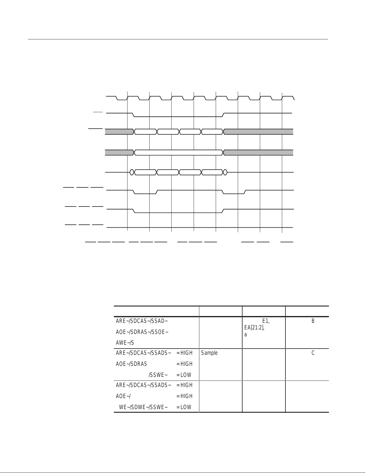
ECLKOUT
Figures 2–1 through 2–6 illustrate the bus timing for the SBSRAM, ASYNC, and
SDRAM memory operations. The Custom Clock is the rising edge of the
ECLKOUT.
CEx
BE(3:0)
EA(21:2)
ED(31:0)
BE1
BE2
BE3 BE4
EA
Q1 Q2 Q3 Q4
ARE/SDCAS/SSADS*
AOE/SDRAS/SSOE
*
AWE/SDWE/SSWE*
ABCDEFGH
Note: *ARE/SDCAS/SSADS, AOE/SDRAS/SSOE and AWE/SDWE/SSWE operate as SSADS, SSOE and SSWE,
respectively, during SBSRAM accesses.
Figure 2–1: Bus timing for the SBSRAM Read cycle with a burst of four data
transitions
2–4
T able 2–1: Signal acquisition in SBSRAM Read cycle
Qualifiers Operation Signals Custom Clock
ARE~/SDCAS~/SSADS~
БББББ
AOE~/SDRAS~/SSOE~
БББББ
AWE~/SDWE~/SSWE~
ARE~/SDCAS~/SSADS~
БББББ
AOE~/SDRAS~/SSOE~
БББББ
AWE~/SDWE~/SSWE~
БББББ
ARE~/SDCAS~/SSADS~
БББББ
AOE~/SDRAS~/SSOE~
БББББ
AWE~/SDWE~/SSWE~
= LOW
ÁÁ
= HIGH
ÁÁ
= HIGH
= HIGH
ÁÁ
= LOW
ÁÁ
= HIGH
ÁÁ
= HIGH
ÁÁ
= LOW
ÁÁ
= HIGH
Sample and
Master
ÁÁÁÁ
ÁÁÁÁ
Sample and
ÁÁÁÁ
Master
ÁÁÁÁ
ÁÁÁÁ
Sample and
Master
ÁÁÁÁ
ÁÁÁÁ
CEx~, BE1,
EA[21:2]
ÁÁÁÁ
ÁÁÁÁ
BE2
ÁÁÁÁ
ÁÁÁÁ
ÁÁÁÁ
BE3, Q1
ÁÁÁÁ
ÁÁÁÁ
At position B
ÁÁÁ
ÁÁÁ
At position C
ÁÁÁ
ÁÁÁ
ÁÁÁ
At position D
ÁÁÁ
ÁÁÁ
TMS711 320C6211/C6711 Microprocessor Support
Page 27

T able 2–1: Signal acquisition in SBSRAM Read cycle (Cont.)
Á
Á
Á
Á
Á
Á
Á
Á
Á
Á
Á
Á
Á
Á
Á
Á
Á
Á
Á
Á
Á
Á
Á
Á
Á
Á
Á
Á
Á
Á
Á
Á
Á
Á
Á
Á
Á
Á
Á
Á
Qualifiers Custom ClockSignalsOperation
ARE~/SDCAS~/SSADS~
БББББ
AOE~/SDRAS~/SSOE~
БББББ
AWE~/SDWE~/SSWE~
БББББ
ARE~/SDCAS~/SSADS~
БББББ
AOE~/SDRAS~/SSOE~
БББББ
AWE~/SDWE~/SSWE~
ARE~/SDCAS~/SSADS~
БББББ
AOE~/SDRAS~/SSOE~
БББББ
AWE~/SDWE~/SSWE~
БББББ
= HIGH
ÁÁ
= LOW
ÁÁ
= HIGH
ÁÁ
= HIGH
ÁÁ
= LOW
ÁÁ
= HIGH
= LOW
ÁÁ
= LOW
ÁÁ
= HIGH
ÁÁ
Sample and
ÁÁÁÁ
Master
ÁÁÁÁ
ÁÁÁÁ
Sample and
Master
ÁÁÁÁ
ÁÁÁÁ
Sample and
ÁÁÁÁ
Master
ÁÁÁÁ
ÁÁÁÁ
BE4, Q2
ÁÁÁ
ÁÁÁ
ÁÁÁ
Q3
ÁÁÁ
ÁÁÁ
Q4
ÁÁÁ
ÁÁÁ
ÁÁÁ
Setting Up the Support
At position E
ÁÁÁÁ
ÁÁÁÁ
ÁÁÁÁ
At position F
ÁÁÁÁ
ÁÁÁÁ
At position G
ÁÁÁÁ
ÁÁÁÁ
ÁÁÁÁ
TMS711 320C6211/C6711 Microprocessor Support
2–5
Page 28
Setting Up the Support
Á
Á
Á
ÁÁÁ
Á
Á
Á
Á
Á
Á
Á
Á
Á
Á
Á
Á
Á
Á
Á
Á
Á
ÁÁÁ
Á
Á
Á
Á
Á
Á
Á
Á
Á
Á
Á
Á
Á
ÁÁÁ
Á
Á
Á
Á
Á
Á
Á
Á
Á
Á
Á
Á
Á
Á
Á
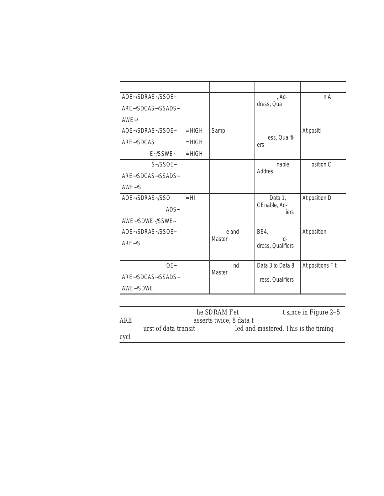
ECLKOUT
Figure 2–2 shows the bus timing for the SBSRAM Write cycle with a burst of 4
data transitions.
CEx
BE(3:0)
EA(21:2)
ED(31:0)
BE1
Q1 Q2 Q3 Q4
BE2 BE3 BE4
EA
ARE/SDCAS/SSADS*
AOE/SDRAS/SSOE
*
AWE/SDWE/SSWE*
ABCDEFGH
Note: *ARE/SDCAS/SSADS, AOE/SDRAS/SSOE and AWE/SDWE/SSWE operate as SSADS, SSOE and SSWE,
respectively, during SBSRAM accesses.
Figure 2–2: SDSRAM Write cycles with a burst of four data transitions
T able 2–2: Signal acquisition in SBSRAM Write cycle
2–6
Qualifiers Operation Signals Custom Clock
ARE~/SDCAS~/SSAD~
ББББББ
AOE~/SDRAS~/SSOE~
ББББББ
AWE~/SDWE~/SSWE~
ББББББ
ARE~/SDCAS~/SSADS~
AOE~/SDRAS~/SSOE~
ББББББ
ББББББ
AWE~/SDWE~/SSWE~
ARE~/SDCAS~/SSADS~
ББББББ
AOE~/SDRAS~/SSOE~
ББББББ
AWE~/SDWE~/SSWE~
ББББББ
= LOW
Á
= HIGH
Á
= LOW
Á
= HIGH
= HIGH
Á
Á
= LOW
= HIGH
Á
= HIGH
Á
= LOW
Á
Sample and
Master
ÁÁÁÁ
ÁÁÁÁ
ÁÁÁÁ
Sample and
Master
ÁÁÁÁ
ÁÁÁÁ
Sample and
Master
ÁÁÁÁ
ÁÁÁÁ
ÁÁÁÁ
CEx~, BE1,
EA[21:2],
ÁÁÁÁ
and Q1
ÁÁÁÁ
ÁÁÁÁ
BE2, Q2
ÁÁÁÁ
ÁÁÁÁ
BE3, Q3
ÁÁÁÁ
ÁÁÁÁ
ÁÁÁÁ
At position B
ÁÁÁ
ÁÁÁ
ÁÁÁ
At position C
ÁÁÁ
ÁÁÁ
At position D
ÁÁÁ
ÁÁÁ
ÁÁÁ
TMS711 320C6211/C6711 Microprocessor Support
Page 29

Á
Á
Á
Á
Á
Á
Á
Á
Á
Á
Á
Á
Á
Á
Á
Á
Á
Á
Á
Á
Á
Á
Á
Á
Á
ECLKOUT
Setting Up the Support
T able 2–2: Signal acquisition in SBSRAM Write cycle (Cont.)
Qualifiers Custom ClockSignalsOperation
ARE~/SDCAS~/SSADS~
БББББ
AOE~/SDRAS~/SSOE~
БББББ
AWE~/SDWE~/SSWE~
БББББ
ARE~/SDCAS~/SSADS~
БББББ
AOE~/SDRAS~/SSOE~
БББББ
AWE~/SDWE~/SSWE~
= HIGH
ÁÁ
= HIGH
ÁÁ
= LOW
ÁÁ
= LOW
ÁÁ
= HIGH
ÁÁ
= HIGH
Sample and
ÁÁÁÁ
Master
ÁÁÁÁ
ÁÁÁÁ
Come out of the
loop
ÁÁÁÁ
ÁÁÁÁ
BE4, Q4
ÁÁÁÁ
ÁÁÁÁ
ÁÁÁÁ
–––
ÁÁÁÁ
ÁÁÁÁ
At position E
ÁÁÁ
ÁÁÁ
ÁÁÁ
At position F
ÁÁÁ
ÁÁÁ
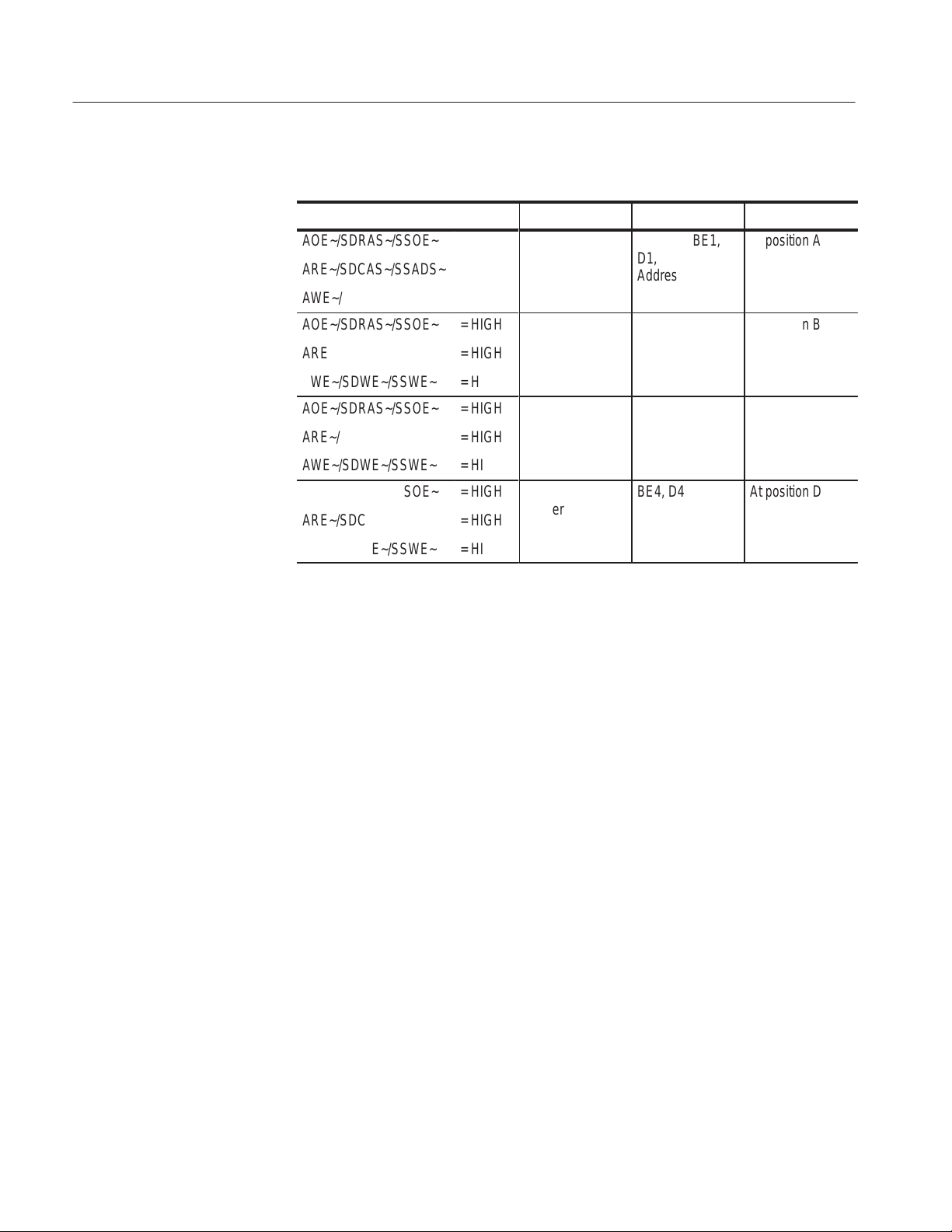
Figure 2–3 shows the bus timing for the ASYNC Read cycle memory operations.
Setup = 2 Strobe = 4 Not ready = 3 Hold = 1
CEx
BE(3:0)
EA(21:2)
ED(31:0)
AOE/SDRAS/SSOE
ARE/SDCAS/SSADS*
AWE/SDWE/SSWE*
*
ABCDEFGH
Note: *ARE
/SDCAS/SSADS, AOE/SDRAS/SSOE and AWE/SDWE/SSWE operate as ARE, AOE and AWE, during
ASYNC accesses. Data group is delated by 1 Clock.
Figure 2–3: Bus timing for the ASYNC read cycle
BE
Address
Read data
TMS711 320C6211/C6711 Microprocessor Support
2–7
Page 30

Setting Up the Support
Á
Á
Á
ÁÁÁ
Á
Á
Á
Á
Á
Á
Á
Á
Á
Á
Á
Á
Á
Á
Á
Á
Á
ÁÁÁ
Á
Á
Á
Á
Á
Á
Á
Á
Á
Á
T able 2–3: Signal acquisition in ASYNC Write cycle
Qualifiers Operation Signals Custom Clock
AOE~/SDRAS~/SSOE~
ББББББ
ARE~/SDCAS~/SSADS~
ББББББ
AWE~/SDWE~/SSWE~
ББББББ
AOE~/SDRAS~/SSOE~
ББББББ
ARE~/SDCAS~/SSADS~
ББББББ
AWE~/SDWE~/SSWE~
= LOW
Á
= LOW
Á
= HIGH
Á
= LOW
Á
= HIGH
Á
= HIGH
Sample
ÁÁÁÁ
ÁÁÁÁ
ÁÁÁÁ
Master
ÁÁÁÁ
ÁÁÁÁ
CEx~, BE,
ÁÁÁÁ
Address, and
Data
ÁÁÁÁ
ÁÁÁÁ
The signals
sampled at
ÁÁÁÁ
position G
ÁÁÁÁ
At positions
ÁÁÁ
A to G
ÁÁÁ
ÁÁÁ
At position H
ÁÁÁ
ÁÁÁ
Figure 2–4 shows the bus timing for the ASYNC Write cycle memory opera-
tions.
Setup = 2 Strobe = 4 Not ready = 3 Hold = 1
ECLKOUT
CEx
BE(3:0)
EA(21:2)
ED(31:0)
ARE/SDRAS/SSOE*
AOE/SDCAS/SSADS
AWE/SDWE/SSWE*
BE
Address
Address
*
ABCDEFGH
Note: *ARE/SDCAS/SSADS, AOE/SDRAS/SSOE and AWE/SDWE/SSWE operate as ARE, AOE and AWE, during
ASYNC accesses.
Figure 2–4: Bus timing for the ASYNC write cycle
2–8
TMS711 320C6211/C6711 Microprocessor Support
Page 31

Setting Up the Support
Á
Á
Á
Á
Á
Á
Á
Á
Á
Á
Á
Á
Á
Á
Á
Á
Á
Á
Á
Á
Á
Á
Á
Á
Á
T able 2–4: Signal acquisition in ASYNC Write cycle
Qualifiers Operation Signals Custom Clock
AOE~/SDRAS~/SSOE~
БББББ
ARE~/SDCAS~/SSADS~
БББББ
AWE~/SDWE~/SSWE~
БББББ
AOE~/SDRAS~/SSOE~
БББББ
ARE~/SDCAS~/SSADS~
БББББ
AWE~/SDWE~/SSWE~
= HIGH
ÁÁ
= HIGH
ÁÁ
= LOW
ÁÁ
= HIGH
ÁÁ
= HIGH
ÁÁ
= HIGH
Sample
ÁÁÁÁ
ÁÁÁÁ
ÁÁÁÁ
Master
ÁÁÁÁ
ÁÁÁÁ
CEx~, BE,
ÁÁÁÁ
Address, and
Data
ÁÁÁÁ
ÁÁÁÁ
The signals
sampled at posi-
ÁÁÁÁ
tion G
ÁÁÁÁ
At positions A to
ÁÁÁ
G
ÁÁÁ
ÁÁÁ
At position H
ÁÁÁ
ÁÁÁ
Figure 2–5 shows a SDRAM Fetch cycle with CAS latency = 3.
Note: *ARE/SDCAS/SSADS, AOE/SDRAS/SSOE and AWE/SDWE/SSWE operate as SDCAS SDRAS and
SDWE
Figure 2–5: Bus timing for the SDRAM fetch cycle with CAS latency of 3
TMS711 320C6211/C6711 Microprocessor Support
, during SDRAM accesses.
2–9
Page 32
Setting Up the Support
Á
Á
Á
ÁÁÁ
Á
Á
Á
Á
Á
Á
Á
Á
Á
Á
Á
Á
Á
Á
Á
Á
Á
ÁÁÁ
Á
Á
Á
Á
Á
Á
Á
Á
Á
Á
Á
Á
Á
ÁÁÁ
Á
Á
Á
Á
Á
Á
Á
Á
Á
Á
Á
Á
Á
Á
Á
Á
Á
ÁÁÁ
Á
Á
Á
Á
Á
Á
Á
Á
Á
Á
Á
Á
Á
ÁÁÁ
Á
Á
Á
Á
Á
Á
Á
Á
Á
Á
Á
Á
Á
Á
Á
Á
Á
ÁÁÁ
Á
Á
Á
Á
Á
Á
Á
Á
Á
Á
T able 2–5: Signal acquisition in SDRAM fetch cycle with CAS latency of 3
Qualifiers Operation Signals Custom Clock
AOE~/SDRAS~/SSOE~
ББББББ
ARE~/SDCAS~/SSADS~
ББББББ
AWE~/SDWE~/SSWE~
ББББББ
AOE~/SDRAS~/SSOE~
ББББББ
ARE~/SDCAS~/SSADS~
ББББББ
AWE~/SDWE~/SSWE~
AOE~/SDRAS~/SSOE~
ББББББ
ARE~/SDCAS~/SSADS~
ББББББ
AWE~/SDWE~/SSWE~
ББББББ
AOE~/SDRAS~/SSOE~
ББББББ
ARE~/SDCAS~/SSADS~
ББББББ
AWE~/SDWE~/SSWE~
AOE~/SDRAS~/SSOE~
ББББББ
ARE~/SDCAS~/SSADS~
ББББББ
AWE~/SDWE~/SSWE~
ББББББ
AOE~/SDRAS~/SSOE~
ББББББ
ARE~/SDCAS~/SSADS~
ББББББ
AWE~/SDWE~/SSWE~
= HIGH
Á
= LOW
Á
= HIGH
Á
= HIGH
Á
= HIGH
Á
= HIGH
= HIGH
Á
= HIGH
Á
= HIGH
Á
= HIGH
Á
= LOW
Á
= HIGH
= HIGH
Á
= HIGH
Á
= HIGH
Á
= HIGH
Á
= HIGH
Á
= HIGH
Sample and
ÁÁÁÁ
Master
ÁÁÁÁ
ÁÁÁÁ
Sample and
Master
ÁÁÁÁ
ÁÁÁÁ
Sample and
ÁÁÁÁ
Master
ÁÁÁÁ
ÁÁÁÁ
Sample and
Master
ÁÁÁÁ
ÁÁÁÁ
Sample and
ÁÁÁÁ
Master
ÁÁÁÁ
ÁÁÁÁ
Sample and
Master
ÁÁÁÁ
ÁÁÁÁ
CEnable, Ad-
ÁÁÁÁ
dress, Qualifiers
ÁÁÁÁ
ÁÁÁÁ
BE1, CEnable,
Address, Qualifi-
ÁÁÁÁ
ers
ÁÁÁÁ
BE2, CEnable,
ÁÁÁÁ
Address, Qualifiers
ÁÁÁÁ
ÁÁÁÁ
BE3, Data 1,
CEnable, Ad-
ÁÁÁÁ
dress, Qualifiers
ÁÁÁÁ
BE4, Data 2,
ÁÁÁÁ
CEnable, Address, Qualifiers
ÁÁÁÁ
ÁÁÁÁ
Data 3 to Data 8,
CEnable, Ad-
ÁÁÁÁ
dress, Qualifiers
ÁÁÁÁ
At position A
ÁÁÁ
ÁÁÁ
ÁÁÁ
At position B
ÁÁÁ
ÁÁÁ
At position C
ÁÁÁ
ÁÁÁ
ÁÁÁ
At position D
ÁÁÁ
ÁÁÁ
At position E
ÁÁÁ
ÁÁÁ
ÁÁÁ
At positions F to
next 5 following
ÁÁÁ
clocks
ÁÁÁ
2–10
NOTE. The default burst in the SDRAM Fetch cycle is 4, but since in Figure 2–5
ARE~/SDCASE~/SSADS~ asserts twice, 8 data transitions appear in the bursts.
So this burst of data transitions was sampled and mastered. This is the timing
cycle behavior usually seen on the logic analyzer.
TMS711 320C6211/C6711 Microprocessor Support
Page 33

Setting Up the Support
Figure 2–6 shows a SDRAM Write cycle with a default of four data transitions.
Write
ECLKOUT
CEx
BE(3:0)
EA(21:13)
EA(11:2)
EA12
ED(31:0)
AOE/SDRAS/SSOE
ARE/SDCAS/SSADS*
AWE/SDWE/SSWE*
BE1 BE2
Bank
Column
D1
*
ABCD
D2
BE3 BE4
D3 D4
Figure 2–6: SDRAM Write cycle with default of four data transitions
TMS711 320C6211/C6711 Microprocessor Support
2–11
Page 34
Setting Up the Support
Á
Á
Á
ÁÁÁ
Á
Á
Á
Á
Á
Á
Á
Á
Á
Á
Á
Á
Á
Á
Á
Á
Á
ÁÁÁ
Á
Á
Á
Á
Á
Á
Á
Á
Á
Á
Á
Á
Á
ÁÁÁ
Á
Á
Á
Á
Á
Á
Á
Á
Á
Á
Á
Á
Á
Á
Á
Á
Á
ÁÁÁ
Á
Á
Á
Á
Á
Á
Á
Á
Á
Á
T able 2–6: Signal acquisiton in SDRAM write cycle with CAS latency of 3
Qualifiers Operation Signals Custom Clock
AOE~/SDRAS~/SSOE~
ББББББ
ARE~/SDCAS~/SSADS~
ББББББ
AWE~/SDWE~/SSWE~
ББББББ
AOE~/SDRAS~/SSOE~
ББББББ
ARE~/SDCAS~/SSADS~
ББББББ
AWE~/SDWE~/SSWE~
AOE~/SDRAS~/SSOE~
ББББББ
ARE~/SDCAS~/SSADS~
ББББББ
AWE~/SDWE~/SSWE~
ББББББ
AOE~/SDRAS~/SSOE~
ББББББ
ARE~/SDCAS~/SSADS~
ББББББ
AWE~/SDWE~/SSWE~
= HIGH
Á
= LOW
Á
= LOW
Á
= HIGH
Á
= HIGH
Á
= HIGH
= HIGH
Á
= HIGH
Á
= HIGH
Á
= HIGH
Á
= HIGH
Á
= HIGH
Sample and
ÁÁÁÁ
Master
ÁÁÁÁ
ÁÁÁÁ
Sample and
Master
ÁÁÁÁ
ÁÁÁÁ
Sample and
ÁÁÁÁ
Master
ÁÁÁÁ
ÁÁÁÁ
Sample and
Master
ÁÁÁÁ
ÁÁÁÁ
CEnable, BE1,
ÁÁÁÁ
D1,
Address,Qualifi-
ÁÁÁÁ
ers
ÁÁÁÁ
BE2, D2
ÁÁÁÁ
ÁÁÁÁ
BE3, D3
ÁÁÁÁ
ÁÁÁÁ
ÁÁÁÁ
BE4, D4
ÁÁÁÁ
ÁÁÁÁ
At position A
ÁÁÁ
ÁÁÁ
ÁÁÁ
At position B
ÁÁÁ
ÁÁÁ
At position C
ÁÁÁ
ÁÁÁ
ÁÁÁ
At position D
ÁÁÁ
ÁÁÁ
2–12
TMS711 320C6211/C6711 Microprocessor Support
Page 35

Acquiring and Viewing Disassembled Data
Acquiring Data
Once you load the C6211/C6711 support, choose a clocking mode, and specify
the trigger, you are ready to acquire and disassemble data.
If you have any problems acquiring data, refer to information on basic operations
in your online help or Appendix A: Error Messages and Disassembly Problems in
the basic operations user manual.
Viewing Disassembled Data
You can view disassembled data in six display formats: Timing, State, Hardware,
Software, Control Flow, and Subroutine. The information on basic operations
describes how to select the disassembly display formats.
NOTE. Selections in the Disassembly property page (the Disassembly Format
Definition overlay) must be set correctly for your acquired data to be disassembled correctly. Refer to Changing How Data is Displayed on page 2–16.
The default display format displays the Address, Data, and Control channel
group values for each sample of acquired data.
If a channel group is not visible, you must use the Disassembly property page to
make the group visible.
The disassembler displays special characters and strings in the instruction
mnemonics to indicate significant events. Table 2–7 lists these special characters
and strings and gives a definition of what they represent.
T able 2–7: Description of special characters in the display
Character or string displayed Definition
>> The instruction was manually marked.
t
Indicates the number shown is in decimal, such as #12t
TMS711 320C6211/C6711 Microprocessor Support
2–13
Page 36

Acquiring and Viewing Disassembled Data
Timing Display Format
Hardware Display Format
The timing-waveform display format file is provided for the TLA 700 Series
support. The timing-waveform display format file will set up and display the
following waveforms:
Address (busform)
Data (busform)
ASYNC (busform)
Control (busform)
CEnable (busform)
BEnable (busform)
ECLKOUT (busform)
In Hardware display format, the disassembler displays certain cycle type labels in
parentheses. Table 2–8 lists cycle type labels and gives a definition of the cycle
they represent. Reads to interrupt and exception vectors will be labeled with the
vector name.
T able 2–8: Cycle type definitions
Cycle Type
( RESET CYCLE )
( ALTERNATE BUS MASTER CYCLE )
Definition
Indicates system RESET
Indicates HOLD cycle
( SDRAM DEAC/DCAB CYCLE )
( SDRAM ACTV CYCLE )
( FLUSH )
( EXTENSION )
( ASYNC READ CYCLE) Indicates ASYNC memory READ cycle
( SBSRAM READ CYCLE) Indicates SBSRAM READ cycle
( SDRAM READ CYCLE) Indicates SDRAM READ cycle
( SBSRAM WRITE CYCLE) Indicates SBSRAM WRITE cycle
( ASYNC WRITE CYCLE) Indicates ASYNC WRITE cycle
( SDRAM WRITE CYCLE) Indicates SDRAM WRITE cycle
( SBSRAM MRS CYCLE )
( UNKNOWN CYCLE )
Indicates SDRAM DEAC or DCAB cycle
Indicates SDRAM ACTV cycle
Indicates a cycle was fetched but not executed
Indicates an extension to the preceding instruction
opcode
Indicates SDRAM MRS cycle
Indicates a combination of control bits are unexpected or
unrecognized
The external address bus has 19 lines EA21:EA2 lines for EMIF (External
Memory Interface). However, the address internal to the processor are 32 bits.
This 32 bit address is calculated based on Byte Enables, Chip Enables (Memory
Space Enables) and user inputs. The Data bus has 32 lines ED31:ED0
2–14
TMS711 320C6211/C6711 Microprocessor Support
Page 37

Acquiring and Viewing Disassembled Data
Figure 2–7 shows an example of a Hardware display.
Software Display Format
Control Flow Display
Format
Subroutine Display
Format
Figure 2–7: Hardware display format
The Software display format displays only the first fetch of executed instructions.
Flushed cycles and extensions are not shown, even though they are part of the
executed instruction. Read extensions will be used to disassemble the instruction,
but they will not be displayed as a separate cycle in the Software display format.
Data reads and writes are not displayed.
The Control Flow display format displays only the first fetch of instructions that
cause a branch in the addressing and special cycles to change the flow of control.
Instructions that generate a change in the flow of control in the C6211/C6711
microprocessor are as follows:
B IRP B disp B NRP B reg
The Subroutine display format displays only the first fetch of subroutine call and
return instructions. It will display conditional subroutine calls if they are
considered to be taken.
Instructions that generate a subroutine call or a return in the C6211/C6711
microprocessor are as follows:
B IRP B NRP
TMS711 320C6211/C6711 Microprocessor Support
2–15
Page 38

Acquiring and Viewing Disassembled Data
Changing How Data is Displayed
There are common fields and features that allow you to further modify displayed
data to suit your needs. You can make common and optional display selections in
the Disassembly property page (the Disassembly Format Definition overlay).
Optional Display
Selections
Micro Specific Fields
You can make optional selections for acquired disassembled data. In addition to
the common selections (described in the information on basic operations), you
can change the displayed data in the following ways:
Show: Hardware (default)
Software
Control Flow
Subroutine
Highlight: Software (default)
Control Flow
Subroutine
None
Disasm Across Gaps: Yes (default)
No
Endian Mode. This field allows the user to indicate a C6211 processor configuration for viewing data from memory. The following selections will be available in
the following order.
Little Endian (default)
Big Endian
2–16
The C6211
memory CE0,CE1,CE2,CE3 where user can read and write. The C6211/C6711
support can have three types of memories, ASYNC, SDRAM, SBSRAM. Any of
these memory types can be allotted to any of the Memory spaces. So the
following user inputs are required to know which memory is allotted to which
memory spaces.
CE0 Space control. The user needs to enter the C6211 CE0 Space control
Register’s value. This field gives the memory type and the buswidth of that
particular memory.
FFFFFF30 (default)
Processor has a single Memory Map. This memory map has four
TMS711 320C6211/C6711 Microprocessor Support
Page 39

Acquiring and Viewing Disassembled Data
CE1 space control. The user needs to enter the C6211 CE1 Space control
Register’s value. This field gives the memory type and the buswidth of that
particular memory.
FFFFFF23 (default)
CE2 space control. The user needs to enter the C6211 CE2 Space control
Register’s value. This field gives the memory type and the buswidth of that
particular memory.
FFFFFF23 (default)
CE3 Space control. The user needs to enter the C6211 CE3 Space control
Register’s value. This field gives the memory type and the buswidth of that
particular memory.
FFFFFF23 (default)
SDRAM Control Register. The user needs to enter the C6211 SDRAM Control
register value. This gives the Row and Column address pins which are required
for address calculation.
06117000 (default)
SDRAM Read Latency . The user needs to enter the CAS latency of SDRAM Read
cycle.
Three (default)
CE0 ST ART ADDR. The user needs to enter the Start address of the CE0 address
space for the board.
80000000 (default)
CE1 ST ART ADDR. The user needs to enter the Start address of the CE1 address
space for the board.
90000000 (default)
CE2 ST ART ADDR. The user needs to enter the Start address of the CE2 address
space for the board.
A0000000 (default)
TMS711 320C6211/C6711 Microprocessor Support
2–17
Page 40

Acquiring and Viewing Disassembled Data
CE3 ST ART ADDR. The user needs to enter the Start address of the CE3 address
space for the board.
B0000000 (default)
SDRAM ADDR Configuration Field. The following Table 2–9 lists the common
configuration of SDRAM that are fully supported by
column SDRAM Address configuration lists numbers 1 through 11. The user must
choose one of these numbers for the appropriate SDRAM Memory configuration
on their board. The default value in in the SDRAM ADDR configuration field is
1. For the TI C6211
DSK kit, the C6211/C6711 support uses 0x3 in the SDRAM
ADDR Configuration Field.
T able 2–9: C6211/C6711 Compatible SDRAM Memory Configuration
C6211/C6711 EMIF. The
SDRAM
size
16
Mbit
64
Mbit
128
Mbit
256
Mbit
AddressMax
Devices/
Banks Width Depth
2 x4 2M 8 16M SDRAM
2
2 x16 512K 2 4M SDRAM
4 x4 4M 8 64M SDRAM
4
4
4 x32 512K 1 8M SDRAM
4 x8 4M 4 64M SDRAM
4 x16 2M 2 32M SDRAM
4 x8 8M 4 128M SDRAM
4 x16 4M 2 64M SDRAM
x8 1M 4 8M SDRAM
x8 2M 4 32M SDRAM
x16 1M 2 16M SDRAM
CE
able
space
(MBytes)
EMIF
EMIF
EMIF
EMIF
EMIF
EMIF
EMIF
EMIF
EMIF
EMIF
EMIF
Column
Address
A9 – A0
EA11 – EA2
A8 – A0
EA10 – EA2
A7 – A0
EA9 – EA2
A9 – A0
EA11 – EA2
A8– A0
EA10 – EA2
A7 – A0
EA9 – EA2
A7 – A0
EA9 – EA2
A9 – A0
EA11 – EA2
A8 – A0
EA10 – EA2
A9 – A0
EA11 – EA2
A8– A0
EA10 – EA2
Row
Address
A10 – A0
EA12 – EA2
A10 – A0
EA12 – EA2
A10 – A0
EA12 – EA2
A11 – A0
EA13 – EA2
A11 – A0
EA13 – EA2
A11 – A0
EA13 – EA2
A10 – A0
EA12 – EA2
A11 – A0
EA13 – EA2
A11– A0
EA13 – EA2
A12 – A0
EA14 – EA2
A12– A0
EA14 – EA2
Bank
Select
A11
EA13
A11
EA13
A11
EA13
A13–A12
EA15–EA14
A13–A12
EA15–EA14
A13–A12
EA15–EA14
A12–A11
EA14–EA13
A13–A12
EA15–EA14
A13–A12
EA15–EA14
A14–A13
EA16–EA15
A14–A13
EA16–EA15
Prechange
A10
EA12
A10
EA12
A10
EA12
A10
EA12
A10
EA12
A10
EA12
A10
EA12
A10
EA12
A10
EA12
A10
EA12
A10
EA12
SDRAM
Address
configuration
1
2
3
4
5
6
7
8
9
10
11
2–18
TMS711 320C6211/C6711 Microprocessor Support
Page 41

Acquiring and Viewing Disassembled Data
The following user input fields for the C6211/C6711 support has a 256 word size
Interrupt Service Table (IST). The IST is a table of fetch packets that contain
code for servicing each of the Interrupts. The IST contains 16 fetch packets. Each
Interrupt Service Routine is 32 bytes. The RESET has the Highest priority, NMI
the second highest, and the lowest priority Interrupts are INT4 to INT15. The
reset fetch packet must be located at address 0, but the rest of the interrupts, NMI
and INT4–INT15, can be relocated anywhere within the IST (256 word
boundary). Also, this IST can be relocated to any address location.
NOTE. Since there are no Interrupt acknowledge signals and signals which tell
which interrupt is being serviced, the user must enter the start address where the
Service-Routine-Fetch packets are located.
NMI_FP_ADDR. The user needs to enter the 32 bit physical address; for example,
Start Address, of the NonMaskable Interrupt-Service-Routine Fetch Packet in the
Interrupt Service Table.
00000020 (default)
INT4_FP_ADDR. The user needs to enter the 32 bit physical address; for example,
Start Address, of the external interrupt EXT_INT4 Service-Routine-Fetch Packet
in the Interrupt Service Table.
00000080 (default)
INT5_FP_ADDR. The user needs to enter the 32 bit physical address; for example,
Start Address, of the external interrupt EXT_INT5 Service-Routine-Fetch Packet
in the Interrupt Service Table.
000000A0 (default)
INT6_FP_ADDR. The user needs to enter the 32 bit physical address; for example,
Start Address, of the external interrupt EXT_INT6 Service-Routine-Fetch Packet
in the Interrupt Service Table.
000000C0 (default)
INT7_FP_ADDR. The user needs to enter the 32 bit physical address; for example,
Start Address, of the external interrupt EXT_INT7 Service-Routine-Fetch Packet
in the Interrupt Service Table.
000000E0 (default)
TMS711 320C6211/C6711 Microprocessor Support
2–19
Page 42

Acquiring and Viewing Disassembled Data
INT8_FP_ADDR. The user needs to enter the 32 bit physical address; for example,
Start Address, of the external interrupt EXT_INT8 Service-Routine-Fetch Packet
in the Interrupt Service Table.
00000100 (default)
INT9_FP_ADDR. The user needs to enter the 32 bit physical address; for example,
Start Address, of the external interrupt EXT_INT9 Service-Routine-Fetch Packet
in the Interrupt Service Table.
00000120 (default)
INT10_FP_ADDR. The user needs to enter the 32 bit physical address; for
example, Start Address, of the external interrupt EXT_INT10 Service-RoutineFetch Packet in the Interrupt Service Table.
00000140 (default)
INT11_FP_ADDR. The user needs to enter the 32 bit physical address; for example,
Start Address of the external interrupt EXT_INT11 Service-Routine-Fetch Packet
in the Interrupt Service Table.
00000160 (default)
INT12_FP_ADDR. The user needs to enter the 32 bit physical address; for
example, Start Address of the external interrupt EXT_INT12 Service-RoutineFetch Packet in the Interrupt Service Table.
00000180 (default)
INT13_FP_ADDR. The user needs to enter the 32 bit physical address; for
example, Start Address of the external interrupt EXT_INT13 Service-RoutineFetch Packet in the Interrupt Service Table.
000001A0 (default)
INT14_FP_ADDR. The user needs to enter the 32 bit physical address; for
example, Start Address of the external interrupt EXT_INT14 Service-RoutineFetch Packet in the Interrupt Service Table.
2–20
000001C0 (default)
TMS711 320C6211/C6711 Microprocessor Support
Page 43

Acquiring and Viewing Disassembled Data
INT15_FP_ADDR. The user needs to enter the 32 bit physical address; for
example, Start Address of the external interrupt EXT_INT15 Service-RoutineFetch Packet in the Interrupt Service Table.
000001E0 (default)
Marking Cycles
TMS711 320C6211/C6711support allows marks to be placed by using the
The
Mark Opcode button. The Mark Opcode will always be available. If the sample
being marked is not an Address cycle or Data cycle of the potential bus master,
the Mark Opcode selections will be replaced by a note indicating that “An
Opcode Mark cannot be placed at the selected data sample.”
When a cycle is marked, this character >> is displayed immediately to the left of
the Mnemonics column. Cycles can be unmarked by using the Undo Mark
selection, which will remove this character >>. If more than one set of sequences
are marked, then the user can undo the marks by using the “Remove all Marks”
option.
The following cycle marks will be available:
H Reads can be marked as Opcode, Fetch, or Flash
H Fetch can be marked as Read or Flush
H Flush can be marked as Fetch or Opcode
Viewing an Example of Disassembled Data
A demonstration system file (or demonstration reference memory) is provided so
you can see an example of how your C6211/C6711 microprocessor bus cycles
and instruction mnemonics look when they are disassembled. Viewing the system
file is not a requirement for preparing the module for use and you can view it
without connecting the logic analyzer to your system under test.
TMS711 320C6211/C6711 Microprocessor Support
2–21
Page 44

Acquiring and Viewing Disassembled Data
2–22
TMS711 320C6211/C6711 Microprocessor Support
Page 45

Specifications
Page 46

Page 47

Specifications
Specification Tables
This chapter contains information regarding the specifications of the TMS711
320C6211/C6711
microprocessor support.
Tables 3–1 and 3–2 list the electrical requirements the system under test must
produce for the TMS711 320C6211/C6711 support to acquire correct data.
T able 3–1: C6211 Electrical specifications
Characteristics Requirements
System under test clock rate
Maximum specified clock rate:
ASYNC memory
SBSRAM memory
SDRAM memory
Tested clock rate
Minimum setup time required † 2.5 ns
Minimum hold time required † 0 ns
* Please contact your Tektronix Sales Representative for current information on the
tested clock rate.
† Logic analyzer setup times are estimated for all signals for the supported memory
cycles. However , you can change both the setup and hold times.
*
100 MHz
100 MHz
100 MHz
100 MHz
TMS711 320C6211/C6711 Microprocessor Support
3–1
Page 48

Specifications
T able 3–2: C6711 Electrical Specifications
Characteristics Requirements
Sytem under test clock rate
Maximum specified clock rate:
ASYNC memory
SBSRAM memory
SDRAM memory
Tested clock rate
Minimum setup time required 2.5 ns
Minimum hold time required 0 ns
* Please contact your Tektronix Sales Representative for current information on the
tested clock rate.
† Logic analyzer setup times are estimated for all signals for the supported memory
cycles. However , you can change both the setup and hold times.
*
100 MHz
100 MHz
100 MHz
–––
3–2
TMS711 320C6211/C6711 Microprocessor Support
Page 49

Replaceable Parts
Page 50

Page 51

Replaceable Parts
This section contains a list of the replaceable parts for the TMS711
320C6211/C6711 C6211/C6711 microprocessor support product.
Parts Ordering Information
Replacement parts are available through your local Tektronix field office or
representative.
Changes to Tektronix products are sometimes made to accommodate improved
components as they become available and to give you the benefit of the latest
improvements. Therefore, when ordering parts, it is important to include the
following information in your order.
H Part number
H Instrument type or model number
H Instrument serial number
H Instrument modification number, if applicable
Abbreviations
Mfr. Code to Manufacturer
Cross Index
If you order a part that has been replaced with a different or improved part, your
local Tektronix field office or representative will contact you concerning any
change in part number.
Abbreviations conform to American National Standard ANSI Y1.1–1972.
The table titled Manufacturers Cross Index shows codes, names, and addresses
of manufacturers or vendors of components listed in the parts list.
TMS711 320C6211/C6711 Microprocessor Support
4–1
Page 52

Replaceable Parts
Manufacturers cross index
Mfr.
code
TK2548 XEROX CORPORATION 14181 SW MILLIKAN WA Y BEAVERT ON, OR 97005
Manufacturer Address City, state, zip code
Replaceable parts list
Fig. &
index
number
Tektronix
part number
071–0877–00 1 MANUAL, TECH: INSTRUCTIONS, C62XX, TMS711 TK2548 071–0877–00
Serial no.
effective
Serial no.
discont’d
Qty Name & description Mfr. code Mfr. part number
STANDARD ACCESSORIES
4–2
TMS711 320C6211/C6711 Microprocessor Support
Page 53

Reference
Page 54

Page 55

Reference: Channel Groups
This section lists the Symbol table and the Channel group tables for disassembly
and timing.
Symbol Table
Table 5–1 lists the name, bit pattern, and meaning for the symbols in the file
C6211_Ctrl, the Control channel group symbol table.
T able 5–1: Control symbol table definitions
Symbol
RESET 0XXXX
HOLD_ACK 10XXX
SDREAD/SBREAD 1 1 1 0 1
ASREAD 11001
SDWRITE/SBWRTIE 11100
ASWRITE 11110
SDRAM_ACTV 11011
SDRAM_DCAB/DEAC 11010
SDRAM_MRS 11000
Control group value
HOLDA~
AOE~/SDRAS~/SSOE~
RESET AWE~/SDWE~/SSWE~
ARE~/SDCAS~/SSADS~
TMS711 320C6211/C6711 Microprocessor Support
5–1
Page 56

Reference:Channel Groups
Channel Assignments
Channel assignments listed in Tables 5–2 through 5–4 use the following
conventions:
H All signals are required by the support unless indicated otherwise.
H Channels are listed starting with the most significant bit (MSB), descending
to the least significant bit (LSB).
H Channel group assignments are for all modules unless otherwise noted.
H An Tilde symbol (~) following a signal name indicates an active low signal.
H An equals symbol (=) following a signal name indicates that it is double
probed.
H The module in the lower-numbered slot is referred to as the HI module and
the module in the lower-numbered slot is referred to as the LO module.
The portable logic analyzer has the lower numbered slots on the top and the
benchtop logic analyzer has the lower numbered slots on the left.
The channel assignment groups will be displayed in the following order:
Group name Display radix
Address Hexadecimal
Data Hexadecimal
Mnemonic None
Control Symbolic
Async Off
CEnable Off
BEnable Off
Misc Off
5–2
TMS711 320C6211/C6711 Microprocessor Support
Page 57

Reference:Channel Groups
Table 5–2 lists the probe section and channel assignments for the Address group
and the microprocessor signal to which each channel connects. By default the
Address channel group assignments are displayed in hexadecimal.
T able 5–2: Address channel group assignments
Bit order Section:channel C6211/C6711 signal name
31 A3:7 NC
21 A2:5 NC
20 A2:4 NC
19 A2:3 EA21
18 A2:2 EA20
17 A2:1 EA19
16 A2:0 EA18
15 A1:7 EA17
14 A1:6 EA16
13 A1:5 EA15
12 A1:4 EA14
11 A1:3 EA13
10 A1:2 EA12
9 A1:1 EA11
8 A1:0 EA10
7 A0:7 EA9
6 A0:6 EA8
5 A0:5 EA7
4 A0:4 EA6
3 A0:3 EA5
2 A0:2 EA4
1 A0:1 EA3
0 A0:0 EA2
Table 5–3 lists the probe section and channel assignments for the Data group and
the microprocessor signal to which each channel connects. By default the Data
channel group assignments are displayed in hexadecimal.
T able 5–3: Data channel group assignments
Bit order Section:channel C6211/C6711 signal name
31 D3:7 ED31
30 D3:6 ED30
TMS711 320C6211/C6711 Microprocessor Support
5–3
Page 58

Reference:Channel Groups
T able 5–3: Data channel group assignments (cont.)
Bit order C6211/C6711 signal nameSection:channel
29 D3:5 ED29
28 D3:4 ED28
27 D3:3 ED27
26 D3:2 ED26
25 D3:1 ED25
24 D3:0 ED24
23 D2:7 ED23
22 D2:6 ED22
21 D2:5 ED21
20 D2:4 ED20
19 D2:3 ED19
18 D2:2 ED18
17 D2:1 ED17
16 D2:0 ED16
15 D1:7 ED15
14 D1:6 ED14
13 D1:5 ED13
12 D1:4 ED12
11 D1:3 ED11
10 D1:2 ED10
9 D1:1 ED9
8 D1:0 ED8
7 D0:7 ED7
6 D0:6 ED6
5 D0:5 ED5
4 D0:4 ED4
3 D0:3 ED3
2 D0:2 ED2
1 D0:1 ED1
0 D0:0 ED0
5–4
TMS711 320C6211/C6711 Microprocessor Support
Page 59

Reference:Channel Groups
Table 5–4 lists the probe section and channel assignments for the Control group
and the microprocessor signal to which each channel connects. The default radix
of the Control group is SYMBOLIC on the logic analyzer. The symbol table file
name is C6211_Ctrl on the logic analyzer.
T able 5–4: Control channel group assignments
Bit order Section:channel C6211/C6711 signal name
4 C2:1 AOE~/SDRAS~/SSOE~
3 C2:0 AWE~/SDWE~/SSWE~
2 C2:2 ARE~/SDCAS~/SSADS~
1 C3:5 HOLDA~
0 C3:6 RESET~
By default Table 5–5 Async channel group assignments are not displayed.
T able 5–5: Async channel group assignments
Bit order Section:channel C6211/C6711 signal name
2 C2:1 AWE~/SDWE~/SSWE~
1 C2:0 ARE~/SDCAS~/SSADS~
0 C2:2 AOE~/SDRAS~/SSOE~
By default Table 5–6 CEnable channel group assignments are not displayed.
T able 5–6: CEnable channel group assignments
Bit order Section:channel C6211/C6711 signal name
3 C1:3 CE3~
2 C1:2 CE2~
1 C1:1 CE1~
0 C1:0 CE0~
By default Table 5–7 BEnable channel group assignments are not displayed.
T able 5–7: BEnable channel group assignments
Bit order Section:channel C6211/C6711 signal name
3 C1:7 BE3~
2 C1:6 BE2~
TMS711 320C6211/C6711 Microprocessor Support
5–5
Page 60

Reference:Channel Groups
T able 5–7: BEnable channel group assignments (cont.)
Bit order C6211/C6711 signal nameSection:channel
1 C1:5 BE1~
0 C1:4 BE0~
By default Table 5–8 Misc channel group assignments are not displayed.
T able 5–8: Misc channel group assignments
Bit order Section:channel C6211/C6711 signal name
0 Clock:3 ECLKOUT
Table 5–9 lists the probe section and clock and qualifier channel assignments.
The clock probes are not part of any group.
T able 5–9: Clock and Qualifier channel assignments
Section:channel C6211/C6711 signal name
CLK:3 ECLKOUT
C2:0 ARE~/SDCAS~/SSADS~
C2:1 AWE~/SDWE~/SSWE~
C2:2 AOE~/SDRAS~/SSOE~
Acquisition Setup. The TMS711 320C6211/C6711support affects the logic
analyzer setup menus (and submenus) by modifying existing fields and adding
micro-specific fields.
The TMS711 320C6211/C6711 support adds the selection C6211 to the Load
Support Package dialog box, under the File pulldown menu. Once the C6211
support has been loaded, the Custom clocking mode selection in the module
Setup menu is also enabled.
5–6
TMS711 320C6211/C6711 Microprocessor Support
Page 61
CPU To Mictor Connections
To probe the microprocessor you will need to make connections between the
CPU and the Mictor pins of the P6434 Mass Termination Probe. Refer to the
P6434 Mass Termination Probe manual, Tektronix part number 070-9793-xx, for
more information on mechanical specifications. Tables 5–10 through 5–16 list
the CPU pin to Mictor pin connections.
Tektronix uses a counterclockwise pin assignment. Pin-1 is located at the top
left, and pin-2 is located directly below it. Pin-20 is located on the bottom right,
and pin-21 is located directly above it.
AMP uses an odd side-even side pin assignment. Pin-1 is located at the top left,
and pin-3 is located directly below it. Pin-2 is located on the top right, and pin-4
is located directly below it (see Figure 5–1).
NOTE. When designing Mictor connectors into your system under test, always
follow the Tektronix pin assignment.
Reference:Channel Groups
Tektronix Pinout AMP Pinout
Pin 1
Pin 19
Pin 38
Pin 20
Pin 1
Pin 37
Pin 2
Pin 38
Figure 5–1: Pin assignments for a Mictor connector (component side)
NOTE. To protect the CPU and the inputs of the module, it is recommended that a
180 W resistor is connected in series between each ball pad of the CPU and each
pin of the Mictor connector. The resistor must be within 1/2 inch of the ball pad
of the CPU.
T able 5–10: CPU to Mictor connections for Mictor A pins
AMP
Logic analyzer
channel
A0:0 EA2 A38 A20
C6211/C6711
signal name
Mictor A
pin number
Tektronix
Mictor A
pin number
A0:1 EA3 A36 A21
A0:2 EA4 A34 A22
TMS711 320C6211/C6711 Microprocessor Support
5–7
Page 62

Reference:Channel Groups
T able 5–10: CPU to Mictor connections for Mictor A pins (cont.)
AMP
Logic analyzer
channel
A0:3 EA5 A32 A23
A0:4 EA6 A30 A24
A0:5 EA7 A28 A25
A0:6 EA8 A26 A26
A0:7 EA9 A24 A27
A1:0 EA10 A22 A28
A1:1 EA11 A20 A29
A1:2 EA12 A18 A30
A1:3 EA13 A16 A31
A1:4 EA14 A14 A32
A1:5 EA15 A12 A33
A1:6 EA16 A10 A34
A1:7 EA17 A8 A35
A2:0 EA18 A37 A19
A2:1 EA19 A35 A18
C6211/C6711
signal name
Mictor A
pin number
Tektronix
Mictor A
pin number
A2:2 EA20 A33 A17
A2:3 EA21 A31 A16
A2:4 NC A29 A15
A2:5 NC A27 A14
A2:6 NC A25 A13
A2:7 NC A23 A12
A3:0 NC A21 A11
A3:1 NC A19 A10
A3:2 NC A17 A9
A3:3 NC A15 A8
A3:4 NC A13 A7
A3:5 NC A11 A6
A3:6 NC A9 A5
A3:7 NC A7 A4
5–8
TMS711 320C6211/C6711 Microprocessor Support
Page 63

T able 5–11: CPU to Mictor connections for Mictor D pins
Reference:Channel Groups
AMP
C6211/C6711
LA channel
D0:0 ED0 D38 D20
D0:1 ED1 D36 D21
D0:2 ED2 D34 D22
D0:3 ED3 D32 D23
D0:4 ED4 D30 D24
D0:5 ED5 D28 D25
D0:6 ED6 D26 D26
D0:7 ED7 D24 D27
D1:0 ED8 D22 D28
D1:1 ED9 D20 D29
D1:2 ED10 D18 D30
D1:3 ED11 D16 D31
D1:4 ED12 D14 D32
D1:5 ED13 D12 D33
D1:6 ED14 D10 D34
signal name
Mictor D
pin number
Tektronix
Mictor D
pin number
D1:7 ED15 D8 D35
D2:0 ED16 D37 D19
D2:1 ED17 D35 D18
D2:2 ED18 D33 D17
D2:3 ED19 D31 D16
D2:4 ED20 D29 D15
D2:5 ED21 D27 D14
D2:6 ED22 D25 D13
D2:7 ED23 D23 D12
D3:0 ED24 D21 D11
D3:1 ED25 D19 D10
D3:2 ED26 D17 D9
D3:3 ED27 D15 D8
D3:4 ED28 D13 D7
D3:5 ED29 D11 D6
TMS711 320C6211/C6711 Microprocessor Support
5–9
Page 64
Reference:Channel Groups
T able 5–11: CPU to Mictor connections for Mictor D pins (cont.)
AMP
C6211/C6711
LA channel
D3:6 ED30 D9 D5
D3:7 ED31 D7 D4
signal name
Mictor D
pin number
Tektronix
Mictor D
pin number
T able 5–12: CPU to Mictor connections for Mictor C pins
AMP
C6211/C6711
LA channel
C2:0 ARE~/SDCAS~/SSADS~ C37 C19
C2:1 AWE~/SDWE~/SSWE~ C35 C18
C2:2 AOE~/SDRAS~/SSOE~ C33 C17
C3:5 HOLDA~ C11 C6
C3:6 RESET~ C9 C5
signal name
Mictor C
pin number
Tektronix
Mictor C
pin number
T able 5–13: CPU to Mictor connections for CEnable
AMP
C6211/C6711
LA channel
C1:0 CE0~ C22 C28
C1:1 CE1~ C20 C29
C1:2 CE2~ C18 C30
C1:3 CE3~ C16 C31
signal name
Mictor C
pin number
Tektronix
Mictor C
pin number
T able 5–14: CPU to Mictor connections for BEnable
AMP
C6211/C6711
LA channel
C1:4 BE0~ C14 C32
C1:5 BE1~ C12 C33
C1:6 BE2~ C10 C34
C1:7 BE3~ C8 C35
signal name
C
Mictor
pin number
Tektronix
Mictor C
pin number
5–10
TMS711 320C6211/C6711 Microprocessor Support
Page 65

T able 5–15: CPU to Mictor connections for Misc
Reference:Channel Groups
AMP
C6211/C6711
LA channel
Clock:3 ECLKOUT C2 C03
signal name
Mictor C
pin number
Tektronix
Mictor
pin number
T able 5–16: CPU to Mictor connections for clock and qualifiers
AMP
C6211/C6711
LA channel
CLK:3 ECLKOUT C2 C03
C2:0 ARE~/SDCAS~/SSADS~
C2:1 AWE~/SDWE~/SSWE~
C2:2 AOE~/SDRAS~/SSOE~
signal name
(Qualifier)
(Qualifier)
(Qualifier)
Mictor C
pin number
C37 C19
C35 C18
C33 C17
Tektronix
Mictor
pin number
C
C
TMS711 320C6211/C6711 Microprocessor Support
5–11
Page 66

Reference:Channel Groups
5–12
TMS711 320C6211/C6711 Microprocessor Support
Page 67

Index
Page 68

Page 69

Index
A
About this manual set, ix
Acquiring data, 2–13
Address, T ektronix, x
Address group, channel assignments, 5–3
Application, logic analyzer configuration, 1–2
Async group, channel assignments, 5–5
B
BEnable group, channel assignments, 5–5
Bus cycles, displayed cycle types, 2–14
C
C6201 clock rate, SUT, 3–1
C6201 loading, 3–1
C6701 clock rate, SUT, 3–2
C6701 loading, 3–2
CE0–3 space control, 2–16
CE0–3 start addr, 2–17
CEnable group, channel assignments, 5–5
Channel assignments
address group, 5–3
Async group, 5–5
BEnable group, 5–5
clocks and qualifiers, 5–6
control group, 5–5
data group, 5–3
Misc group, 5–6
channel assignments, CEnable group, 5–5
Channel groups, 2–1
visibility , 2–13
Clock channel assignments, 5–6
Clock rate, 1–2
Clocking, custom, 2–2
Clocking Options
external clocking, 2–2
internal clocking, 2–2
Clocking options, memory types, 2–3
Connections
CPU to Mictor, 5–7
No probe adapter, 1–5
no probe adapter, 1–5
Contacting T ektronix, x
Control flow display format, 2–15
Control group
channel assignments, 5–5
symbol table, 5–1
CPU to Mictor connections, 5–7
Custom clocking, 2–2
Cycle types, 2–14
D
Data
acquiring, 2–13
disassembly formats
control Flow, 2-15
hardware, 2-14
software, 2-15
subroutine, 2-15
Disassemlby formats, Timing-Display, 2–14
Data display , changing, 2–16
Data group, channel assignments, 5–3
Definitions
disassembler, ix
information on basic operations, ix
Demonstration file, 2–21
Disassembled data
cycle type definitions, 2–14
viewing, 2–13
viewing an example, 2–21
Disassembler
definition, ix
logic analyzer configuration, 1–2
setup, 2–1
Disassembly format definition overlay, 2–16
Disassembly property page, 2–16
Display formats
control Flow, 2–15
hardware, 2–14
software, 2–15
special characters, 2–13
subroutine, 2–15
Timing-Display, 2–14
E
Electrical specifications, 3–1
C6201, 3–1
C6201 clock rate, 3–1
C6701 clock rate, 3–2
TMS711 320C6211/C6711 Microprocessor Support
Index–1
Page 70

Index
C6701 loading, 3–2
H
Hardware display format, 2–14
cycle type definitions, 2–14
Hold time, minimum, 3–1, 3–2
I
Installing support software, 2–1
IST (Interrupt service table), 2–18
codes for servicing interrupts, 2–19
L
Logic analyzer
configuration for disassembler, 1–2
configuration for the application, 1–2
software compatibility, 1–1
M
Manual
conventions, ix
how to use the set, ix
Mark Cycle function, 2–21
Mark Opcode function, 2–21
Marking cycles, definition of, 2–21
Micro Specific Fields
CE0–3 start addr, 2–17
CE0–3space control, 2–16
interrupt service routines, 2–19
Interrupt service table (IST), 2–18
SDRAM addr configuration, 2–18
SDRAM control register, 2–17
SDRAM read latency, 2–17
Mictor to CPU connections, 5–7
Misc group, channel assignments, 5–6
Reference memory, 2–21
Restrictions, 1–2
without a probe adapter, 1–5
S
SDRAM addr configuration, 2–18
SDRAM control register, 2–17
SDRAM read latency, 2–17
Service support, contact information, x
Set up time, minimum, 3–1, 3–2
Setups
disassembler, 2–1
support, 2–1
Software display format, 2–15
Special characters displayed, 2–13
Specifications, 3–1
electrical, 3–1
Subroutine display format, 2–15
Support, setup, 2–1
Support package setups
disassemlby, 2–2
timing, 2–2
Support setup, 2–1
Symbol table, control channel group, 5–1
System file, demonstration, 2–21
T
T echnical support, contact information, x
T ektronix, contacting, x
T erminology, ix
Timing-display format, 2–14
U
URL, T ektronix, x
V
P
Phone number, Tektronix, x
Probe adapter, not using one, 1–5
Product support, contact information, x
R
Reference, channel assignments, 5–2
Index–2
Viewing disassembled data, 2–13
W
Web site address, Tektronix, x
TMS711 320C6211/C6711 Microprocessor Support
 Loading...