

Page 1

Instruction Manual
TMS 710
TMS320C6201/6701 Microprocessor Support
071-0202-01
Warning
The servicing instructions are for use by
qualified personnel only. To avoid personal
injury, do not perform any servicing unless you
are qualified to do so. Refer to all safety
summaries prior to performing service.
Page 2

Copyright E T ektronix, Inc. All rights reserved. Licensed software products are owned by Tektronix or its suppliers and are
protected by United States copyright laws and international treaty provisions.
Use, duplication, or disclosure by the Government is subject to restrictions as set forth in subparagraph (c)(1)(ii) of the
Rights in T echnical Data and Computer Software clause at DFARS 252.227-7013, or subparagraphs (c)(1) and (2) of the
Commercial Computer Software – Restricted Rights clause at F AR 52.227-19, as applicable.
T ektronix products are covered by U.S. and foreign patents, issued and pending. Information in this publication supercedes
that in all previously published material. Specifications and price change privileges reserved.
Printed in the U.S.A.
T ektronix, Inc., P.O. Box 1000, Wilsonville, OR 97070–1000
TEKTRONIX and TEK are registered trademarks of T ektronix, Inc.
Page 3

SOFTWARE WARRANTY
T ektronix warrants that the media on which this software product is furnished and the encoding of the programs on
the media will be free from defects in materials and workmanship for a period of three (3) months from the date of
shipment. If a medium or encoding proves defective during the warranty period, T ektronix will provide a
replacement in exchange for the defective medium. Except as to the media on which this software product is
furnished, this software product is provided “as is” without warranty of any kind, either express or implied.
T ektronix does not warrant that the functions contained in this software product will meet Customer’s
requirements or that the operation of the programs will be uninterrupted or error-free.
In order to obtain service under this warranty, Customer must notify Tektronix of the defect before the expiration
of the warranty period. If T ektronix is unable to provide a replacement that is free from defects in materials and
workmanship within a reasonable time thereafter, Customer may terminate the license for this software product
and return this software product and any associated materials for credit or refund.
THIS WARRANTY IS GIVEN BY TEKTRONIX IN LIEU OF ANY OTHER WARRANTIES, EXPRESS
OR IMPLIED. TEKTRONIX AND ITS VENDORS DISCLAIM ANY IMPLIED WARRANTIES OF
MERCHANTABILITY OR FITNESS FOR A PARTICULAR PURPOSE. TEKTRONIX’
RESPONSIBILITY TO REPLACE DEFECTIVE MEDIA OR REFUND CUSTOMER’S PAYMENT IS
THE SOLE AND EXCLUSIVE REMEDY PROVIDED TO THE CUSTOMER FOR BREACH OF THIS
WARRANTY. TEKTRONIX AND ITS VENDORS WILL NOT BE LIABLE FOR ANY INDIRECT,
SPECIAL, INCIDENTAL, OR CONSEQUENTIAL DAMAGES IRRESPECTIVE OF WHETHER
TEKTRONIX OR THE VENDOR HAS ADVANCE NOTICE OF THE POSSIBILITY OF SUCH
DAMAGES.
Page 4

Page 5

Table of Contents
Getting Started
Operating Basics
General Safety Summary v. . . . . . . . . . . . . . . . . . . . . . . . . . . . . . . . . . . .
Service Safety Summary vii. . . . . . . . . . . . . . . . . . . . . . . . . . . . . . . . . . . . .
Preface ix. . . . . . . . . . . . . . . . . . . . . . . . . . . . . . . . . . . . . . . . . . . . . . . . . . .
Manual Conventions ix. . . . . . . . . . . . . . . . . . . . . . . . . . . . . . . . . . . . . . . . . . . . . .
Contacting T ektronix x. . . . . . . . . . . . . . . . . . . . . . . . . . . . . . . . . . . . . . . . . . . . . .
Support Package Description 1–1. . . . . . . . . . . . . . . . . . . . . . . . . . . . . . . . . . . . . . . .
Logic Analyzer Software Compatibility 1–1. . . . . . . . . . . . . . . . . . . . . . . . . . . . . . .
Logic Analyzer Configuration 1–1. . . . . . . . . . . . . . . . . . . . . . . . . . . . . . . . . . . . . . .
Requirements and Restrictions 1–2. . . . . . . . . . . . . . . . . . . . . . . . . . . . . . . . . . . . . . .
Functionality Not Supported 1–3. . . . . . . . . . . . . . . . . . . . . . . . . . . . . . . . . . . . . . . .
DAS Mass T ermination Interface (MTIF) Probes 1–3. . . . . . . . . . . . . . . . . . . . . . . .
Connecting the Logic Analyzer to a System Under T est 1–3. . . . . . . . . . . . . . . . . . .
Channel Assignments 1–4. . . . . . . . . . . . . . . . . . . . . . . . . . . . . . . . . . . . . . . . . . . . .
CPU To Mictor Connections 1–10. . . . . . . . . . . . . . . . . . . . . . . . . . . . . . . . . . . . . . . .
Setting Up the Support 2–1. . . . . . . . . . . . . . . . . . . . . . . . . . . . . . . . . . . . . .
Channel Group Definitions 2–1. . . . . . . . . . . . . . . . . . . . . . . . . . . . . . . . . . . . . . . . .
Clocking 2–1. . . . . . . . . . . . . . . . . . . . . . . . . . . . . . . . . . . . . . . . . . . . . . . . . . . . . . . .
Symbols 2–9. . . . . . . . . . . . . . . . . . . . . . . . . . . . . . . . . . . . . . . . . . . . . . . . . . . . . . . .
Logic Analyzer Time Alignment for the C6201 2–10. . . . . . . . . . . . . . . . . . . . . . . . .
Logic Analyzer Time Alignment for the C6701 2–18. . . . . . . . . . . . . . . . . . . . . . . . .
Acquiring and Viewing Disassembled Data 2–25. . . . . . . . . . . . . . . . . . . . .
Acquiring Data 2–25. . . . . . . . . . . . . . . . . . . . . . . . . . . . . . . . . . . . . . . . . . . . . . . . . . .
Viewing Disassembled Data 2–25. . . . . . . . . . . . . . . . . . . . . . . . . . . . . . . . . . . . . . . .
Timing Display Format 2–26. . . . . . . . . . . . . . . . . . . . . . . . . . . . . . . . . . . . . . . . .
State-Listing Display Format 2–26. . . . . . . . . . . . . . . . . . . . . . . . . . . . . . . . . . . .
Hardware Display Format 2–26. . . . . . . . . . . . . . . . . . . . . . . . . . . . . . . . . . . . . . .
Software Display Format 2–28. . . . . . . . . . . . . . . . . . . . . . . . . . . . . . . . . . . . . . .
Control Flow Display Format 2–28. . . . . . . . . . . . . . . . . . . . . . . . . . . . . . . . . . . .
Subroutine Display Format 2–28. . . . . . . . . . . . . . . . . . . . . . . . . . . . . . . . . . . . . .
Changing How Data is Displayed 2–28. . . . . . . . . . . . . . . . . . . . . . . . . . . . . . . . . . . .
Optional Display Selections 2–28. . . . . . . . . . . . . . . . . . . . . . . . . . . . . . . . . . . . .
Micro Specific Fields 2–29. . . . . . . . . . . . . . . . . . . . . . . . . . . . . . . . . . . . . . . . . .
Marking Cycles 2–30. . . . . . . . . . . . . . . . . . . . . . . . . . . . . . . . . . . . . . . . . . . . . . .
Displaying Exception Vectors 2–31. . . . . . . . . . . . . . . . . . . . . . . . . . . . . . . . . . . .
Viewing an Example of Disassembled Data 2–31. . . . . . . . . . . . . . . . . . . . . . . . . . . .
Specifications
Replaceable Parts
Index
TMS 710 TMS320C6201/C6701 Microprocessor Support
i
Page 6

Table of Contents
List of Figures
Figure 1–1: Pin assignments for a Mictor connector
(component side) 1–11. . . . . . . . . . . . . . . . . . . . . . . . . . . . . . . . . . . . . . . .
Figure 2–1: Bus timing for the ASYNC Memory Read operation 2–2. . .
Figure 2–2: Bus timing for the ASYNC Memory Write operation 2–3. .
Figure 2–3: Bus timing for the SBSRAM Memory Read operation 2–4. .
Figure 2–4: Bus timing for the SBSRAM Memory Write operation 2–5.
Figure 2–5: Bus timing for the SDRAM Memory Read operation 2–6. . .
Figure 2–6: Bus timing for the SDRAM Memory Write operation 2–7. .
Figure 2–7: Bus timing for the SDRAM row address activation cycle 2–8
Figure 2–8: C6201 Setup: Load System menu 2–10. . . . . . . . . . . . . . . . . . .
Figure 2–9: C6201 Load System Options dialog box 2–11. . . . . . . . . . . . . .
Figure 2–10: C6201 System window with the C6201 Cal Setup file 2–12. .
Figure 2–11: C6201 Custom options C6201 dialog box 2–13. . . . . . . . . . . .
Figure 2–12: C6201 Trigger setup for any asynchronous memory
Read 2–13. . . . . . . . . . . . . . . . . . . . . . . . . . . . . . . . . . . . . . . . . . . . . . . . . .
Figure 2–13: C6201 Asynchronous memory read timing diagram 2–14. . .
Figure 2–14: C6201 Trigger setup for any SBSRAM memory
Read 2–15. . . . . . . . . . . . . . . . . . . . . . . . . . . . . . . . . . . . . . . . . . . . . . . . . .
Figure 2–15: C6201 SBSRAM memory read timing (full-rate SSCLK)
diagram 2–16. . . . . . . . . . . . . . . . . . . . . . . . . . . . . . . . . . . . . . . . . . . . . . .
Figure 2–16: C6201 Custom options C6201 dialog box 2–17. . . . . . . . . . . .
Figure 2–17: C6701 Setup: Load System menu 2–18. . . . . . . . . . . . . . . . . .
Figure 2–18: C6701 Load System Options dialog box 2–19. . . . . . . . . . . . .
Figure 2–19: C6701 System window with the Cal Setup file 2–20. . . . . . . .
Figure 2–20: C6201 Custom options C6201 dialog box 2–20. . . . . . . . . . . .
Figure 2–21: C6701 Custom options dialog box 2–21. . . . . . . . . . . . . . . . . .
Figure 2–22: C6701 Trigger setup for any asynchronous memory
Read 2–21. . . . . . . . . . . . . . . . . . . . . . . . . . . . . . . . . . . . . . . . . . . . . . . . . .
Figure 2–23: C6701 Asynchronous memory read timing diagram 2–22. . .
Figure 2–24: C6701 Trigger setup for any SBSRAM memory Read 2–23.
Figure 2–25: C6701 Custom options dialog box 2–24. . . . . . . . . . . . . . . . . .
Figure 2–25: Hardware display format 2–27. . . . . . . . . . . . . . . . . . . . . . . . .
ii
TMS 710 TMS320C6201/C6701 Microprocessor Support
Page 7

List of Tables
Table of Contents
Table 1–1: Module compatibility specifications 1–2. . . . . . . . . . . . . . . . .
Table 1–2: Address channel group assignments 1–4. . . . . . . . . . . . . . . . .
Table 1–3: Data channel group assignments 1–5. . . . . . . . . . . . . . . . . . . .
Table 1–4: AsyncCtrl channel group assignments 1–6. . . . . . . . . . . . . . . .
Table 1–5: SbsramCtrl channel group assignments 1–7. . . . . . . . . . . . . .
Table 1–6: SdramCtrl channel group assignments 1–7. . . . . . . . . . . . . . .
Table 1–7: Control channel group assignments 1–7. . . . . . . . . . . . . . . . . .
Table 1–8: ByteEnbl channel group assignments 1–8. . . . . . . . . . . . . . . .
Table 1–9: CESpace channel group assignments 1–8. . . . . . . . . . . . . . . . .
Table 1–10: Intr channel group assignments 1–8. . . . . . . . . . . . . . . . . . . .
Table 1–11: Misc channel group assignments 1–9. . . . . . . . . . . . . . . . . . .
Table 1–12: Clock and Qualifier channel assignments 1–9. . . . . . . . . . . .
Table 1–13: Signals not required for clocking and disassembly 1–10. . . .
Table 1–14: CPU to Mictor connections for Mictor A pins 1–11. . . . . . . .
Table 1–15: CPU to Mictor connections for Mictor D pins 1–13. . . . . . . .
Table 1–16: CPU to Mictor connections for Mictor C pins 1–14. . . . . . . .
Table 2–1: Control group symbol table definitions 2–9. . . . . . . . . . . . . . .
Table 2–2: C6201 Memory types and maximum frequencies 2–10. . . . . . .
Table 2–3: C6201 Setup time for the AsyncCtrl group 2–15. . . . . . . . . . . .
Table 2–4: C6201 Setup time for the SbsramCtrl group 2–16. . . . . . . . . . .
Table 2–5: C6701 Memory types and maximum frequencies 2–18. . . . . . .
Table 2–6: C6701 Setup time for the AsyncCtrl group 2–23. . . . . . . . . . . .
Table 2–7: Description of special characters in the display 2–25. . . . . . . .
Table 2–8: Cycle type definitions 2–26. . . . . . . . . . . . . . . . . . . . . . . . . . . . .
Table 2–9: Exception vectors 2–31. . . . . . . . . . . . . . . . . . . . . . . . . . . . . . . . .
Table 3–1: C6201 Electrical specifications 3–1. . . . . . . . . . . . . . . . . . . . .
Table 3–2: C6701 Electrical Specifications 3–1. . . . . . . . . . . . . . . . . . . . .
TMS 710 TMS320C6201/C6701 Microprocessor Support
iii
Page 8

Table of Contents
iv
TMS 710 TMS320C6201/C6701 Microprocessor Support
Page 9

General Safety Summary
Review the following safety precautions to avoid injury and prevent damage to
this product or any products connected to it. To avoid potential hazards, use this
product only as specified.
Only qualified personnel should perform service procedures.
While using this product, you may need to access other parts of the system. Read
the General Safety Summary in other system manuals for warnings and cautions
related to operating the system.
Connect and Disconnect Properly . Do not connect or disconnect probes or test
leads while they are connected to a voltage source.
Ground the Product. This product is indirectly grounded through the grounding
conductor of the mainframe power cord. To avoid electric shock, the grounding
conductor must be connected to earth ground. Before making connections to the
input or output terminals of the product, ensure that the product is properly
grounded.
Observe All Terminal Ratings. To avoid fire or shock hazard, observe all ratings
and marking on the product. Consult the product manual for further ratings
information before making connections to the product.
Symbols and Terms
Do not apply a potential to any terminal, including the common terminal, that
exceeds the maximum rating of that terminal.
Do Not Operate Without Covers. Do not operate this product with covers or panels
removed.
Avoid Exposed Circuitry. Do not touch exposed connections and components
when power is present.
Do Not Operate With Suspected Failures. If you suspect there is damage to this
product, have it inspected by qualified service personnel.
Do Not Operate in Wet/Damp Conditions.
Do Not Operate in an Explosive Atmosphere.
Keep Product Surfaces Clean and Dry .
Provide Proper Ventilation. Refer to the manual’s installation instructions for
details on installing the product so it has proper ventilation.
T erms in this Manual. These terms may appear in this manual:
TMS 710 TMS320C6201/C6701 Microprocessor Support
v
Page 10
General Safety Summary
WARNING. Warning statements identify conditions or practices that could result
in injury or loss of life.
CAUTION. Caution statements identify conditions or practices that could result in
damage to this product or other property.
T erms on the Product. These terms may appear on the product:
DANGER indicates an injury hazard immediately accessible as you read the
marking.
WARNING indicates an injury hazard not immediately accessible as you read the
marking.
CAUTION indicates a hazard to property including the product.
Symbols on the Product. The following symbols may appear on the product:
Protective Ground
(Earth) T erminal
CAUTION
Refer to Manual
vi
TMS 710 TMS320C6201/C6701 Microprocessor Support
Page 11

Service Safety Summary
Only qualified personnel should perform service procedures. Read this Service
Safety Summary and the General Safety Summary before performing any service
procedures.
Do Not Service Alone. Do not perform internal service or adjustments of this
product unless another person capable of rendering first aid and resuscitation is
present.
Disconnect Power. To avoid electric shock, disconnect the main power by means
of the power cord or, if provided, the power switch.
Use Care When Servicing With Power On. Dangerous voltages or currents may
exist in this product. Disconnect power, remove battery (if applicable), and
disconnect test leads before removing protective panels, soldering, or replacing
components.
To avoid electric shock, do not touch exposed connections.
TMS 710 TMS320C6201/C6701 Microprocessor Support
vii
Page 12

Service Safety Summary
viii
TMS 710 TMS320C6201/C6701 Microprocessor Support
Page 13

Preface
Manual Conventions
This instruction manual contains specific information about the
TMS 710 TMS320C6201/C6701 microprocessor support package and is part of a
set of information on how to operate this product on compatible Tektronix logic
analyzers.
If you are familiar with operating microprocessor support packages on the logic
analyzer for which the TMS 710 TMS320C6201/C6701 support was purchased,
you will only need this instruction manual to set up and run the support.
If you are not familiar with operating microprocessor support packages, you will
need to supplement this instruction manual with information on basic operations
to set up and run the support. See Manual Conventions below for more information.
This manual uses the following conventions:
H The term “disassembler” refers to the software that disassembles bus cycles
into instruction mnemonics and cycle types.
H The phrase “information on basic operations” refers to online help, an
installation manual, or a user manual covering the basic operations of
microprocessor support.
TMS 710 TMS320C6201/C6701 Microprocessor Support
ix
Page 14

Preface
Contacting Tektronix
Product
Support
Service
Support
For other
information
To write us Tektronix, Inc.
For application-oriented questions about a Tektronix measurement product, call toll free in North America:
1-800-TEK-WIDE (1-800-835-9433 ext. 2400)
6:00 a.m. – 5:00 p.m. Pacific time
Or, contact us by e-mail:
tm_app_supp@tek.com
For product support outside of North America, contact your
local Tektronix distributor or sales office.
Contact your local Tektronix distributor or sales office. Or, visit
our web site for a listing of worldwide service locations.
tektronix.com
In North America:
1-800-TEK-WIDE (1-800-835-9433)
An operator will direct your call.
P.O. Box 1000
Wilsonville, OR 97070-1000
x
TMS 710 TMS320C6201/C6701 Microprocessor Support
Page 15

Getting Started
Page 16

Page 17

Getting Started
This chapter contains information on the TMS 710 TMS320C6201/C6701
microprocessor support package, and information on connecting your logic
analyzer to your system under test.
Support Package Description
The TMS 710 TMS320C6201/C6701microprocessor support package displays
disassembled data from systems based on the Texas Instruments C6201/C6701
microprocessor.
To use this support efficiently, you need to have the items listed in the information on basic operations and the following documents:
H C62X/C67X CPU and Instruction SET Reference Guide, Texas Instruments,
Feb 24 1998, PRU189C.
H C6201/C6701 Peripheral Reference Guide, Texas Instruments, March 1998,
SPRU190A.
H C6701 Data sheet Texas Instruments, May 1998, SPRS067.
H C6201 Data sheet Texas Instruments, March 1998, SPRS051C.
Information on basic operations also contains a general description of support.
Logic Analyzer Software Compatibility
The floppy disk label on the microprocessor support states which version of logic
analyzer software this support is compatible with.
Logic Analyzer Configuration
The TMS 710 TMS320C6201/C6701support requires a minimum of one
102-channel module.
TMS 710 TMS320C6201/C6701 Microprocessor Support
1–1
Page 18

Getting Started
The TMS 710 support will function with the Logic Analyzer acquisition
modules. Table 1–1 lists the module compatibility specifications.
T able 1–1: Module compatibility specifications
Characteristics Requirements
Tektronix Logic Analyzer
Maximum bus speed 200 MHz
Note:
CK0, CK1, CK2, and CK3 clock channels are stored
Requirements and Restrictions
You should review the general requirements and restrictions of microprocessor
support packages in the information on basic operations as they pertain to your
system under test.
System Clock Rate
Non Intrusive Acquisition
Disabling the Instruction
Cache
Byte Invalidation
You should also review electrical, environmental, and mechanical specifications
in Specifications on page 3–1 as they pertain to your system under test, as well as
the following descriptions of other C6201/C6701 support requirements and
restrictions.
The operating speeds that the C6201/C6701
C6201/C6701 microprocessor are listed on Table 3–1. These specification were
valid at the time this manual was printed. Please contact your Tektronix Sales
Representative for current information on the fastest devices supported.
Acquiring microprocessor bus cycles will be non intrusive to the system under
test. That is, the C6201/C6701 support will not intercept, modify, or present
signals back to the system under test.
To display disassembled acquired data, you must disable the internal instruction
cache. Disabling the cache makes all instruction prefetches visible on the bus
they then can be acquired and displayed disassembled.
Invalid bytes cannot be dashed out during read cycles since byte enables are not
asserted during read cycles.
support can acquire data from the
1–2
TMS 710 TMS320C6201/C6701 Microprocessor Support
Page 19

Getting Started
Opcode Fetch/Data Read.
The C6201/C6701 does not provide a signal to distinguish between Data Read
and Opcode Fetch. The TMS 710 TMS320C6201/C6701 support makes a
reasonable estimate at looking at the address values of a few sequences around
the current sequence. Yet in some instances you may need to use the Mark
Opcode function.
Functionality Not Supported
Microprocessor
Alternate Bus master
The signals: DMA, HPI, MCBSP 0 & 1, and JTAG are not acquired. If you want
to view these signals, you need to find an alternate way to probe them.
Alternative bus master transactions are acquired by the C6201/C6701 support
and are not disassembled.
DAS Mass Termination Interface (MTIF) Probes
The MTIF probes are already labeled since the probe sections for each probe are
permanent. The TMS 710 TMS320C6201/C6701 support channel assignments
follow the standard channel mapping.
Connecting the Logic Analyzer to a System Under Test
You can use channel probes, clock probes, and leadsets with a commercial test
clip (or adapter) to make connections between the logic analyzer and your system
under test.
To connect the probes to C6201/C6701 signals in the system under test using a
test clip, follow these steps:
1. Turn off power to your system under test. It is not necessary to turn off
power to the logic analyzer.
CAUTION. Static discharge can damage the microprocessor, the probes, and the
logic analyzer module. To prevent static damage, handle these components only
in a static-free environment.
Always wear a grounding wrist strap, heel strap, or similar device while
handling the microprocessor.
2. To discharge your stored static electricity, touch the ground connector located
on the back of the logic analyzer. If you are using a test clip, touch any of the
ground pins on the clip to discharge stored static electricity from the test clip.
TMS 710 TMS320C6201/C6701 Microprocessor Support
1–3
Page 20

Getting Started
Channel Assignments
CAUTION. Failure to place the system under test on a horizontal surface before
connecting the test clip can permanently damage the pins on the microprocessor.
3. Place the system under test on a horizontal static-free surface.
4. Use Tables 1–2 through 1–10 to connect the channel probes to C6201/C6701
signal pins on the test clip or in the system under test.
Use leadsets to connect at least one ground lead from each channel probe and
the ground lead from each clock probe to ground pins on your test clip.
Channel assignments listed in Tables 1–2 through 1–10 use the following
conventions:
H All signals are required by the support unless indicated otherwise.
H Channels are listed starting with the most significant bit (MSB), descending
to the least significant bit (LSB).
H Channel group assignments are for all modules unless otherwise noted.
H An asterisk symbol (*) following a signal name indicates an active low
signal.
H An equals symbol (=) following a signal name indicates that it is double
probed.
Table 1–2 lists the probe section and channel assignments for the Address group
and the microprocessor signal to which each channel connects. By default the
Address channel group assignments are displayed in hexadecimal.
T able 1–2: Address channel group assignments
Bit order Section:channel C6201/C6701 signal name
31 A3:7 GND
30 A3:6 GND
29 A3:5 GND
28 A3:4 GND
27 A3:3 GND
26 A3:2 GND
25 A3:1 GND
24 A3:0 GND
23 A2:7 GND
1–4
TMS 710 TMS320C6201/C6701 Microprocessor Support
Page 21

T able 1–2: Address channel group assignments (cont.)
Bit order C6201/C6701 signal nameSection:channel
22 A2:6 GND
21 A2:5 EA21
20 A2:4 EA20
19 A2:3 EA19
18 A2:2 EA18
17 A2:1 EA17
16 A2:0 EA16
15 A1:7 EA15
14 A1:6 EA14
13 A1:5 EA13
12 A1:4 EA12
11 A1:3 EA11
10 A1:2 EA10
9 A1:1 EA9
8 A1:0 EA8
7 A0:7 EA7
6 A0:6 EA6
5 A0:5 EA5
4 A0:4 EA4
3 A0:3 EA3
2 A0:2 EA2
1 A0:1 GND
0 A0:0 GND
Getting Started
Table 1–3 lists the probe section and channel assignments for the Data group and
the microprocessor signal to which each channel connects. By default the Data
channel group assignments are displayed in hexadecimal.
T able 1–3: Data channel group assignments
Bit order Section:channel C6201/C6701 signal name
31 D3:7 ED31
30 D3:6 ED30
29 D3:5 ED29
28 D3:4 ED28
27 D3:3 ED27
26 D3:2 ED26
TMS 710 TMS320C6201/C6701 Microprocessor Support
1–5
Page 22

Getting Started
T able 1–3: Data channel group assignments (cont.)
Bit order C6201/C6701 signal nameSection:channel
25 D3:1 ED25
24 D3:0 ED24
23 D2:7 ED23
22 D2:6 ED22
21 D2:5 ED21
20 D2:4 ED20
19 D2:3 ED19
18 D2:2 ED18
17 D2:1 ED17
16 D2:0 ED16
15 D1:7 ED15
14 D1:6 ED14
13 D1:5 ED13
12 D1:4 ED12
11 D1:3 ED11
10 D1:2 ED10
9 D1:1 ED9
8 D1:0 ED8
7 D0:7 ED7
6 D0:6 ED6
5 D0:5 ED5
4 D0:4 ED4
3 D0:3 ED3
2 D0:2 ED2
1 D0:1 ED1
0 D0:0 ED0
1–6
Tables 1–4 through 1–6 appear only in the TLA 700 Series.
By default Table 1–4 AsyncCtrl channel group assignments are not displayed.
T able 1–4: AsyncCtrl channel group assignments
Bit order Section:channel C6201/C6701 signal name
3 C3:3 ARE*
2 C3:5 AWE *
TMS 710 TMS320C6201/C6701 Microprocessor Support
Page 23

Getting Started
T able 1–4: AsyncCtrl channel group assignments (cont.)
Bit order C6201/C6701 signal nameSection:channel
1 CLK:0 ARE* =
0 C2:3 AWE*=
By default Table 1–5 SbsramCtrl channel group assignments are not displayed.
T able 1–5: SbsramCtrl channel group assignments
Bit order Section:channel C6201/C6701 signal name
3 C2:6 SSADS*
2 C2:5 SSOE*
1 C2:2 SSWE*
0 Qual:0 SSADS*=
By default Table 1–6 SdramCtrl channel group assignments are not displayed.
T able 1–6: SdramCtrl channel group assignments
Bit order Section:channel C6201/C6701 signal name
3 C2:0 SDRAS*
2 C2:1 SDCAS*
1 C3:0 SDWE*
0 Qual:1 SDWE*=
Table 1–7 lists the probe section and channel assignments for the Control group
and the microprocessor signal to which each channel connects. The default radix
of the Control group is SYMBOLIC on the TLA 700. The symbol table file name
is C6201/C6701_Ctrl on the TLA 700.
T able 1–7: Control channel group assignments
Bit order Section:channel C6201/C6701 signal name
10 C3:1 RESET*
9 C3:2 LENDIAN
8 C0:6 HOLDA*
7 C2:0 SDRAS*
6 C2:1 SDCAS*
5 C3:0 SDWE*
TMS 710 TMS320C6201/C6701 Microprocessor Support
1–7
Page 24

Getting Started
T able 1–7: Control channel group assignments (cont.)
Bit order C6201/C6701 signal nameSection:channel
4 C2:6 SSADS*
3 C2:5 SSOE*
2 C2:2 SSWE*
1 C3:3 ARE*
0 C3:5 AWE*
By default Table 1–8 ByteEnbl channel group assignments are not displayed.
T able 1–8: ByteEnbl channel group assignments
Bit order Section:channel C6201/C6701 signal name
3 C1:7 BE3*
2 C1:6 BE2*
1 C1:5 BE1*
0 C1:4 BE0*
By default Table 1–9 CESpace channel group assignments are not displayed.
T able 1–9: CESpace channel group assignments
Bit order Section:channel C6201/C6701 signal name
3 C1:3 CE3*
2 C1:2 CE2*
1 C1:1 CE1*
0 C1:0 CE0*
By default Table 1–10 Intr channel group assignments are not displayed.
T able 1–10: Intr channel group assignments
Bit order Section:channel C6201/C6701 signal name
5 C0:0 IACK
4 C0:1 NMI
3 C0:2 INUM0
2 C0:3 INUM1
1–8
TMS 710 TMS320C6201/C6701 Microprocessor Support
Page 25

Getting Started
T able 1–10: Intr channel group assignments (cont.)
Bit order C6201/C6701 signal nameSection:channel
1 C0:4 INUM2
0 C0:5 INUM3
By default Table 1–11 Misc channel group assignments are not displayed.
T able 1–11: Misc channel group assignments
Bit order Section:channel C6201/C6701 signal name
5 C2:4 CLKOUT1
4 C3:7 CLKOUT2
3 C2:7 SDA10
2 C3:6 ARDY
1 C3:4 AOE*
0 C0:7 HOLD*
Table 1–12 lists the probe section and clock and qualifier channel assignments.
The clock probes are not part of any group.
T able 1–12: Clock and Qualifier channel assignments
Section:channel C6201/C6701 signal name
CLK:0 ARE*=
CLK:1 SSCLK
CLK:2 SDCLK
CLK:3 CLKOUT1=
C2:0 SDRAS*
C2:1 SDCAS*
C2:2 SSWE*
C2:3 A WE*=
QUAL:0 SSADS*=
QUAL:1 SDWE*=
TMS 710 TMS320C6201/C6701 Microprocessor Support
1–9
Page 26

Getting Started
Table 1–13 lists the C6201/C6701 signals not required by the Clocking State
Machine (CSM) or disassembler. The C6201/C6701 signals can be removed from
their default connections and reattached to other signals of interest.
T able 1–13: Signals not required for clocking and disassembly
Signal name Section:channel
IACK,NMI,INUM0–3
CLKOUT1
CLKOUT2
SDA10
ARDY
AOE*
HOLD*
1
2
2
2
2
2
1
Intr group
2
Misc group
1
C0:0 – 5
C2:4
C3:7
C2:7
C3:6
C3:4
C0:7
Acquisition Setup. The TMS 710 TMS320C6201/C6701support affects the logic
analyzer setup menus (and submenus) by modifying existing fields and adding
micro-specific fields.
The TMS 710 TMS320C6201/C6701 support adds the selection C62XX to the
Load Support Package dialog box, under the File pulldown menu. Once the
C62XX support has been loaded, the Custom clocking mode selection in the
module Setup menu is also enabled.
CPU To Mictor Connections
To probe the microprocessor you will need to make connections between the
CPU and the Mictor pins of the P6434 Mass Termination Probe. Refer to the
P6434 Mass Termination Probe manual, Tektronix part number 070-9793-xx, for
more information on mechanical specifications. Tables 1–14 through 1–16 list
the CPU pin to Mictor pin connections.
Tektronix uses a counterclockwise pin assignment. Pin-1 is located at the top left,
and pin-2 is located directly below it. Pin-20 is located on the bottom right, and
pin-21 is located directly above it.
AMP uses an odd side-even side pin assignment. Pin-1 is located at the top left,
and pin-3 is located directly below it. Pin-2 is located on the top right, and pin-4
is located directly below it (see Figure 1–1).
1–10
TMS 710 TMS320C6201/C6701 Microprocessor Support
Page 27

Getting Started
NOTE. When designing Mictor connectors into your system under test, always
follow the Tektronix pin assignment.
Tektronix Pinout AMP Pinout
Pin 1
Pin 19
Pin 38
Pin 20
Pin 1
Pin 37
Pin 2
Pin 38
Figure 1–1: Pin assignments for a Mictor connector (component side)
NOTE. To protect the CPU and the inputs of the module, it is recommended that a
180 W resistor is connected in series between each ball pad of the CPU and each
pin of the Mictor connector. The resistor must be within 1/2 inch of the ball pad
of the CPU.
T able 1–14: CPU to Mictor connections for Mictor A pins
Tektronix
Mictor A
pin number
1 1 NC NC NC
2 3 NC NC NC
3 5 CLOCK:0 ARE*= Y24
4 7 A3:7 GND GND
5 9 A3:6 GND GND
6 11 A3:5 GND GND
7 13 A3:4 GND GND
8 15 A3:3 GND GND
9 17 A3:2 GND GND
10 19 A3:1 GND GND
11 21 A3:0 GND GND
12 23 A2:7 GND GND
13 25 A2:6 GND GND
14 27 A2:5 EA21 J26
15 29 A2:4 EA20 K25
16 31 A2:3 EA19 L24
AMP
Mictor A
pin number
Logic analyzer
channel
C6201/C6701
signal name
Pin number
TMS 710 TMS320C6201/C6701 Microprocessor Support
1–11
Page 28

Getting Started
T able 1–14: CPU to Mictor connections for Mictor A pins (cont.)
Tektronix
Mictor A
pin number
17 33 A2:2 EA18 K26
18 35 A2:1 EA17 M26
19 37 A2:0 EA16 M25
20 38 A0:0 GND GND
21 36 A0:1 GND GND
22 34 A0:2 EA2 Y26
23 32 A0:3 EA3 W25
24 30 A0:4 EA4 V24
25 28 A0:5 EA5 W26
26 26 A0:6 EA6 V25
27 24 A0:7 EA7 V26
28 22 A1:0 EA8 T23
29 20 A1:1 EA9 U25
30 18 A1:2 EA10 U26
31 16 A1:3 EA11 R23
32 14 A1:4 EA12 T26
33 12 A1:5 EA13 R25
34 10 A1:6 EA14 P24
35 8 A1:7 EA15 P25
36 6 CLOCK:1 SSCLK AD17
37 4 NC NC NC
38 2 NC NC NC
39 39 GND GND GND
40 40 GND GND GND
41 41 GND GND GND
42 42 GND GND GND
43 43 GND GND GND
AMP
Mictor A
pin number
Logic analyzer
channel
C6201/C6701
signal name
Pin number
1–12
44 44 GND GND GND
TMS 710 TMS320C6201/C6701 Microprocessor Support
Page 29

T able 1–15: CPU to Mictor connections for Mictor D pins
Getting Started
Tektronix
Mictor D
pin number
1 1 NC NC NC
2 3 NC NC NC
3 5 Qual:0 SSADS*= AC20
4 7 D3:7 ED31 AB2
5 9 D3:6 ED30 AC1
6 11 D3:5 ED29 AA4
7 13 D3:4 ED28 AD1
8 15 D3:3 ED27 AC3
9 17 D3:2 ED26 AD4
10 19 D3:1 ED25 AF3
11 21 D3:0 ED24 AE4
12 23 D2:7 ED23 AD5
13 25 D2:6 ED22 AF4
14 27 D2:5 ED21 AE5
15 29 D2:4 ED20 AD6
16 31 D2:3 ED19 AE6
17 33 D2:2 ED18 AD7
18 35 D2:1 ED17 AC8
19 37 D2:0 ED16 AF7
20 38 D0:0 ED0 AC17
21 36 D0:1 ED1 AF19
22 34 D0:2 ED2 AF18
23 32 D0:3 ED3 AE17
24 30 D0:4 ED4 AC15
25 28 D0:5 ED5 AF16
26 26 D0:6 ED6 AE15
27 24 D0:7 ED7 AF15
28 22 D1:0 ED8 AE14
29 20 D1:1 ED9 AF11
30 18 D1:2 ED10 AE11
31 16 D1:3 ED11 AE10
32 14 D1:4 ED12 AC11
33 12 D1:5 ED13 AF9
34 10 D1:6 ED14 AD10
35 8 D1:7 ED15 AD9
AMP
Mictor D
pin number
LA channel
C6201/C6701
signal name
Pin number
TMS 710 TMS320C6201/C6701 Microprocessor Support
1–13
Page 30

Getting Started
T able 1–15: CPU to Mictor connections for Mictor D pins (cont.)
Tektronix
Mictor D
pin number
36 6 CLOCK:2 SDCLK AE20
37 4 NC NC NC
38 2 NC NC NC
39 39 GND GND GND
40 40 GND GND GND
41 41 GND GND GND
42 42 GND GND GND
43 43 GND GND GND
44 44 GND GND GND
AMP
Mictor D
pin number
LA channel
C6201/C6701
signal name
Pin number
T able 1–16: CPU to Mictor connections for Mictor C pins
TektronixMictor C
pin number
1 1 NC NC NC
2 3 NC NC NC
3 5 CLOCK:3 CLKOUT1= AF22
4 7 C3:7 CLKOUT2 AF20
5 9 C3:6 ARDY W23
6 11 C3:5 AWE* AD23
7 13 C3:4 AOE* AC24
8 15 C3:3 ARE* Y24
9 17 C3:2 LENDIAN H3
10 19 C3:1 RESET* K2
11 21 C3:0 SDWE* AF23
12 23 C2:7 SDA10 AD21
13 25 C2:6 SSADS* AC20
14 27 C2:5 SSOE* AF21
15 29 C2:4 CLKOUT1 AF22
16 31 C2:3 AWE*= AD23
17 33 C2:2 SSWE* AD19
18 35 C2:1 SDCAS* AD22
19 37 C2:0 SDRAS* AF24
20 38 C0:0 IACK Y2
AMP
Mictor C
pin number
LA channel
C6201/C6701
signal name
Pin number
1–14
TMS 710 TMS320C6201/C6701 Microprocessor Support
Page 31

T able 1–16: CPU to Mictor connections for Mictor C pins (cont.)
Getting Started
Tektronix-
Mictor C
pin number
21 36 C0:1 NMI L2
22 34 C0:2 INUM0 AB1
23 32 C0:3 INUM1 AA2
24 30 C0:4 INUM2 W4
25 28 C0:5 INUM3 AA1
26 26 C0:6 HOLDA* A7
27 24 C0:7 HOLD* AA25
28 22 C1:0 CE0* AC26
29 20 C1:1 CE1* AB24
30 18 C1:2 CE2* AD26
31 16 C1:3 CE3* AE22
32 14 C1:4 BE0* AA26
33 12 C1:5 BE1* Y23
34 10 C1:6 BE2* AA24
35 8 C1:7 BE3* AB25
36 6 Qual:1 SDWE*= AF23
37 4 NC NC NC
38 2 NC NC NC
39 39 GND GND GND
40 40 GND GND GND
41 41 GND GND GND
42 42 GND GND GND
43 44 GND GND GND
44 44 GND GND GND
AMP
Mictor C
pin number
LA channel
C6201/C6701
signal name
Pin number
TMS 710 TMS320C6201/C6701 Microprocessor Support
1–15
Page 32

Getting Started
1–16
TMS 710 TMS320C6201/C6701 Microprocessor Support
Page 33

Operating Basics
Page 34

Page 35

Setting Up the Support
The information in this section is specific to the operations and functions of the
TMS 710 TMS320C6201/C6701 microprocessor support on any Tektronix logic
analyzer for which it can be purchased.
Before you acquire and display disassembled data, you need to load the support
and specify setups for clocking and triggering as described in the information on
basic operations. The microprocessor support provides default values for each of
these setups as well as user-definable settings.
Channel Group Definitions
The software automatically defines channel groups for the support. The channel
groups for the TMS 710 TMS320C6201/C6701 support are Address, Data,
Control, AsyncCtrl, SbsramCtrl, SdramCtrl, ByteEnbl, CESpace, Intr, and Misc.
Clocking
Options
Custom Clocking
The TMS 710 TMS320C6201/C6701support offers a microprocessor-specific
clocking mode for the C6201/C6701 microprocessor. This clocking mode is the
default selection whenever you load the TMS 710 TMS320C6201/C6701
support.
Disassembly will not be correct with the Internal or External clocking modes.
Information on basic operations describes how to use these clock selections for
general purpose analysis.
When Custom is selected, the Custom Clocking Options menu will have the
subtitle C6201/C6701 Microprocessor Clocking Support added, and the clocking
options will also be displayed.
The TMS 710 TMS320C6201/C6701support has three clock state machines
(CSM). There is one select field with the label Memory Type: that field will
contain the following selections: ASYNC, SBSRAM, and SDRAM.
Memory operation type:
ASYNC Selects CSM for ASYNC (default)
SBSRAM Selects CSM for SBSRAM
SDRAM Selects CSM for SDRAM
TMS 710 TMS320C6201/C6701 Microprocessor Support
2–1
Page 36
Setting Up the Support
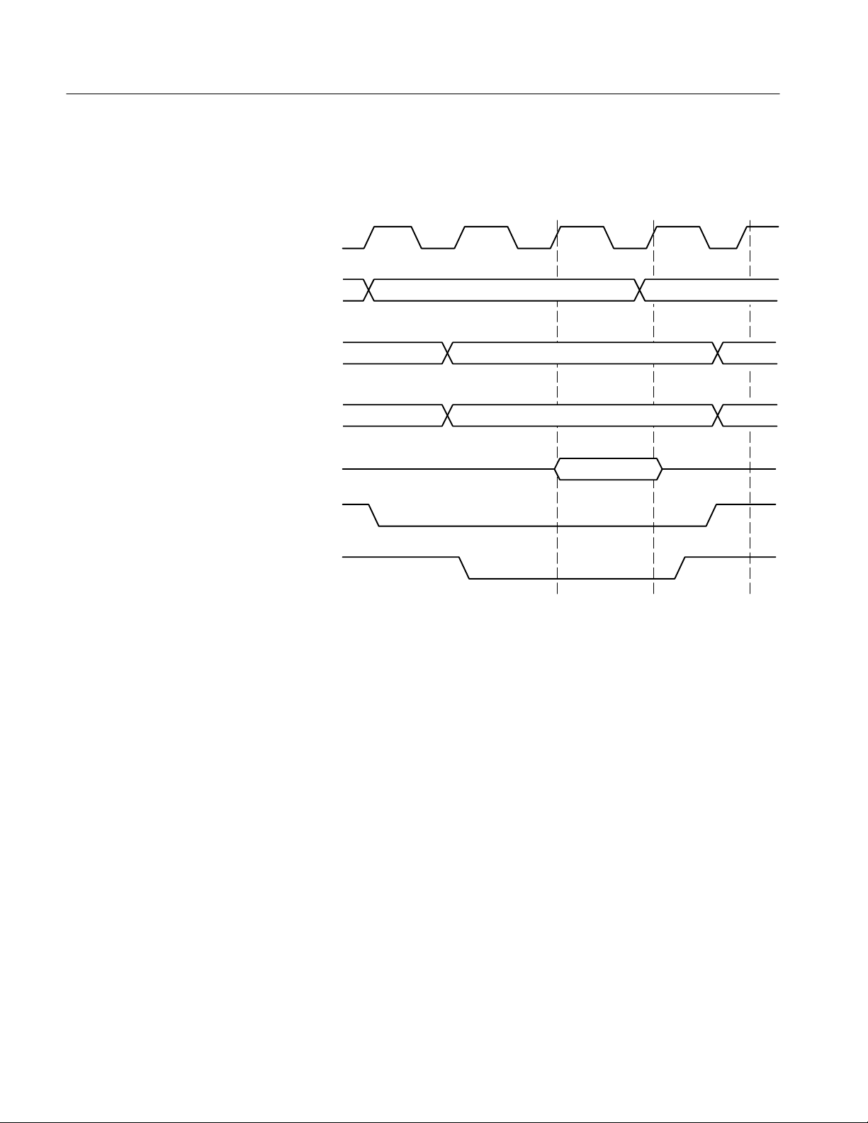
Figures 2–1 through 2–7 illustrate the bus timing for the ASYNC, SBSRAM and
SDRAM memory operations.
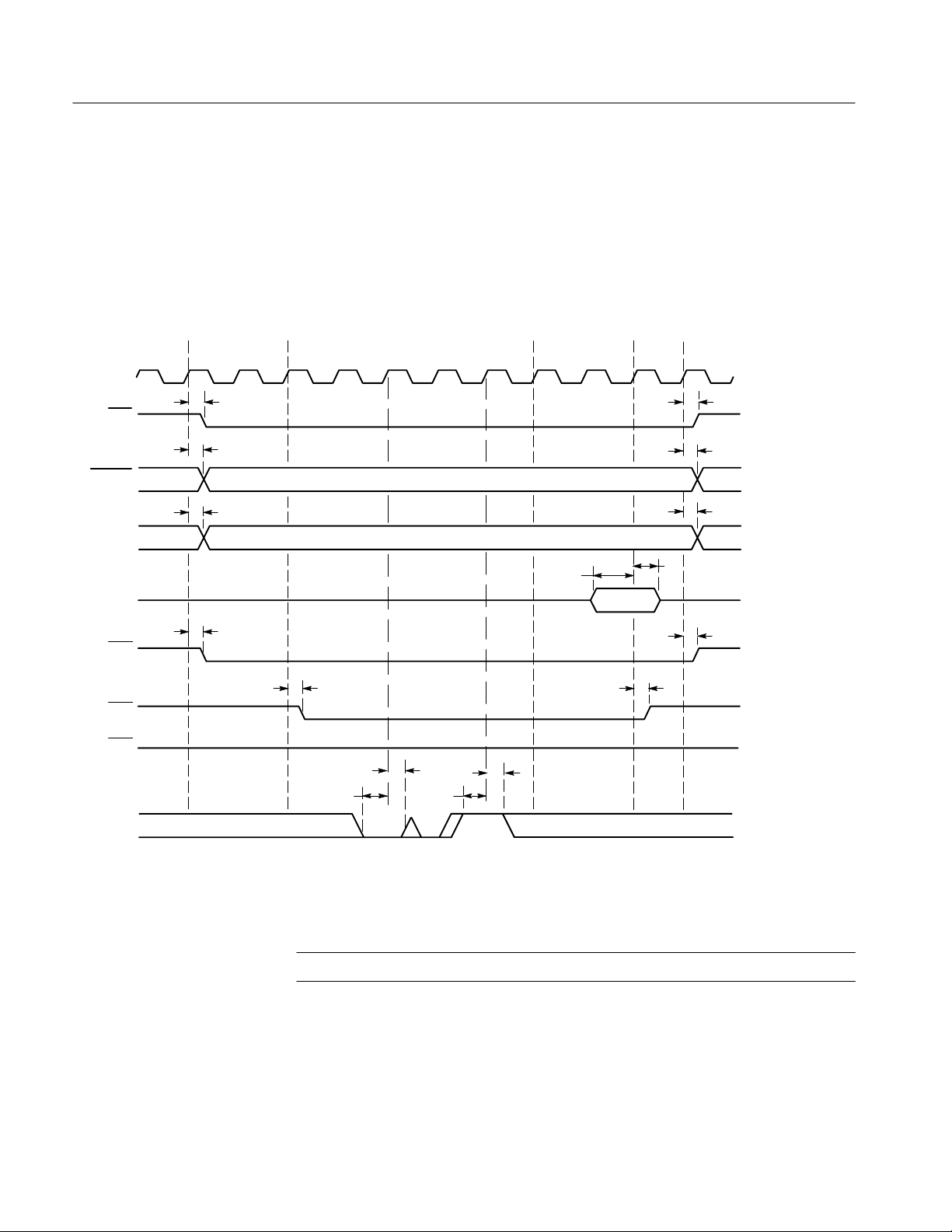
Clkout 1
EA [2–21]
Delayed
EA [2–21]
Delayed
BE [0–3]
ED [0–31]
Delayed CEx*
ARE*
Address
Address
Byte enables
Data
A, C, D M
A, C, D
Figure 2–1: Bus timing for the ASYNC Memory Read operation
2–2
TMS 710 TMS320C6201/C6701 Microprocessor Support
Page 37
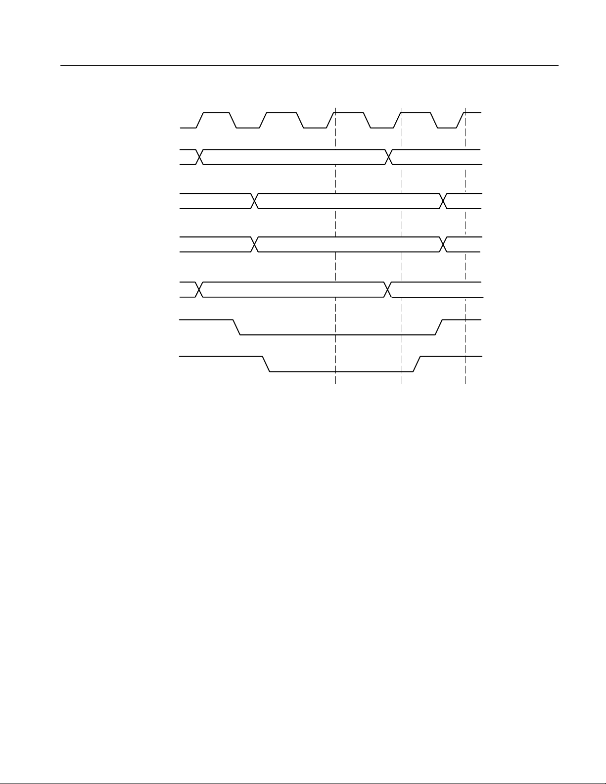
Clkout 1
Setting Up the Support
EA [2–21]
Delayed
EA [2–21]
Delayed
BE [0–3]
ED [0–31]
Delayed CEx*
AWE*
Address
Address
Byte enables
Data
A, C, D
A, C, D M
Figure 2–2: Bus timing for the ASYNC Memory Write operation
TMS 710 TMS320C6201/C6701 Microprocessor Support
2–3
Page 38

Setting Up the Support
SSCLK
CEx*
BE [0–3]
EA [2–21]
ED [0–31]
SSADS*
SSWE*
BE1
A, C, D, M A, C, D, M A, C, D, M A, C, D, M
BE2
A2A1
D1 D2
Figure 2–3: Bus timing for the SBSRAM Memory Read operation
2–4
TMS 710 TMS320C6201/C6701 Microprocessor Support
Page 39

SSCLK
CEx*
Setting Up the Support
BE [0–3]
EA [2–21]
ED [0–31]
SSADS*
SSWE*
BE1
A, C, D, M A, C, D, M
BE2
A2A1
D2D1
Figure 2–4: Bus timing for the SBSRAM Memory Write operation
TMS 710 TMS320C6201/C6701 Microprocessor Support
2–5
Page 40

Setting Up the Support
SSCLK
CEx*
BE [0–3]
EA [2–21]
ED [0–31]
SDCAS*
SDWE*
A, C, D, M A, C, D, M A, C, D, M A, C, D, M A, C, D, M
BE1
CA2CA1
BE2
BE2
Figure 2–5: Bus timing for the SDRAM Memory Read operation
D1 D2
2–6
TMS 710 TMS320C6201/C6701 Microprocessor Support
Page 41

SSCLK
CEx*
Setting Up the Support
BE [0–3]
EA [2–21]
ED [0–31]
SDCAS*
SDWE*
BE1
A, C, D, M A, C, D, M
BE2
BE2
BE2CA1 CA2
BE2D1 D2
Figure 2–6: Bus timing for the SDRAM Memory Write operation
TMS 710 TMS320C6201/C6701 Microprocessor Support
2–7
Page 42

Setting Up the Support
SDCLK
CEx*
BE [0–3]
EA [2–21]
SDRAM Row Address
ED [0–31]
SDRAS*
SSWE*
A, C, D, M
Figure 2–7: Bus timing for the SDRAM row address activation cycle
2–8
TMS 710 TMS320C6201/C6701 Microprocessor Support
Page 43

Symbols
Setting Up the Support
The TMS 710 TMS320C6201/C6701support supplies one symbol table file. The
C6201/C6701_Ctrl file replaces specific Control channel group values with
symbolic values when Symbolic is the radix for the channel group.
Symbol tables are generally not for use in timing or C6201/C6701_T support
disassembly.
Table 2–1 lists the name, bit pattern, and description for the symbols in the
C6201/C6701_Ctrl, in the Control channel group symbol table.
T able 2–1: Control group symbol table definitions
Control group value
RESET* SDCAS* SSWE*
LENDIAN SDWE* ARE*
Symbol
RESET
Alt Master
Cycle
SDRAM Row
Addr
SDRAM Write
SDRAM Read
SDRAM MRS
SBSRAM
Read
SDRAM/
SBSRAM
Read
SBSRAM
Write
ASYNC Read
ASYNC Write
HOLDA* SSADS* AWE*
SDRAS* SSOE*
0XXX XXXX XXX
1X0X XXXX XXX
1X10 1111 111
1X11 0011 111
1X11 0111 111
1X10 0011 111
1X1X XX00 111
1X1X XXXX 111
1X1X XX01 011
1X1X XX11 101
1X1X XX11 110
Description
Processor in Reset
Alternate Bus Master
cycle
SDRAM Row Address
cycle
Write cycle to SDRAM
Read cycle to SDRAM
Sets the mode register of
SDRAM
Read cycle to SBSRAM
Read cycle to SDRAM or
SBSRAM
Write cycle to SBSRAM
Read cycle to ASYNC
Write cycle to ASYNC
TMS 710 TMS320C6201/C6701 Microprocessor Support
2–9
Page 44

Setting Up the Support
Logic Analyzer Time Alignment for the C6201
The setup time alignment of the logic analyzer to a system under test may be
necessary if the C6201
in Table 2–2 with similar memory types. To ensure that the logic analyzer
acquires correct data at higher clock speeds, you may need to follow these
procedures and make the setup timing adjustments.
T able 2–2: C6201 Memory types and maximum frequencies
Memory type
microprocessor operates at a frequency greater than listed
TMS 710 C6201 supported
maximum frequencies
without alignment
C6201 maximum
Asynchronous
SBSRAM
SDRAM
115 MHz
180 MHz
200 MHz
200 MHz
200 MHz
200 MHz
For the Asynchronous and SBSRAM memories, the supported maximum
frequency can be increased by following step 1 through step 18. A setup time
alignment procedure is not included for the SDRAM memory, since the memory
operates at the supported maximum frequency.
1. From the System window in the File menu, select Load System.
2. From the Load System dialog box, browse to where the Cal_Setup.tla file is
located. Figure 2–8 shows the Load System window with the Cal_Setup.tla
system setups.
2–10
Figure 2–8: C6201 Setup: Load System menu
TMS 710 TMS320C6201/C6701 Microprocessor Support
Page 45

Setting Up the Support
3. Select the Cal_Setup.tla file and click open. Click No in the caution dialog
box. If an Information dialog box appears, click OK.
The Load System Options dialog box may or may not appear.
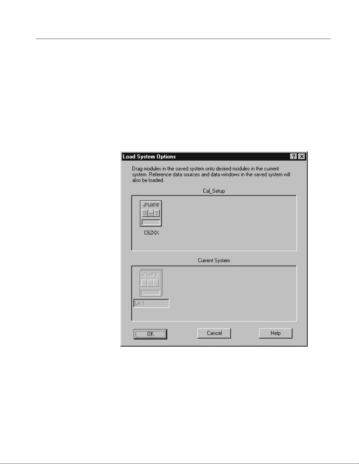
4. If the Load System Options dialog box appears and the C62XX setup is not
loaded to the Current System, then drag the C62XX icon to the desired
module and click OK. If an information box appears click OK.
Figure 2–9 shows the Load System Options dialog box before dragging the
C6201 icon to the module in the Current System.
Figure 2–9: C6201 Load System Options dialog box
TMS 710 TMS320C6201/C6701 Microprocessor Support
2–11
Page 46

Setting Up the Support
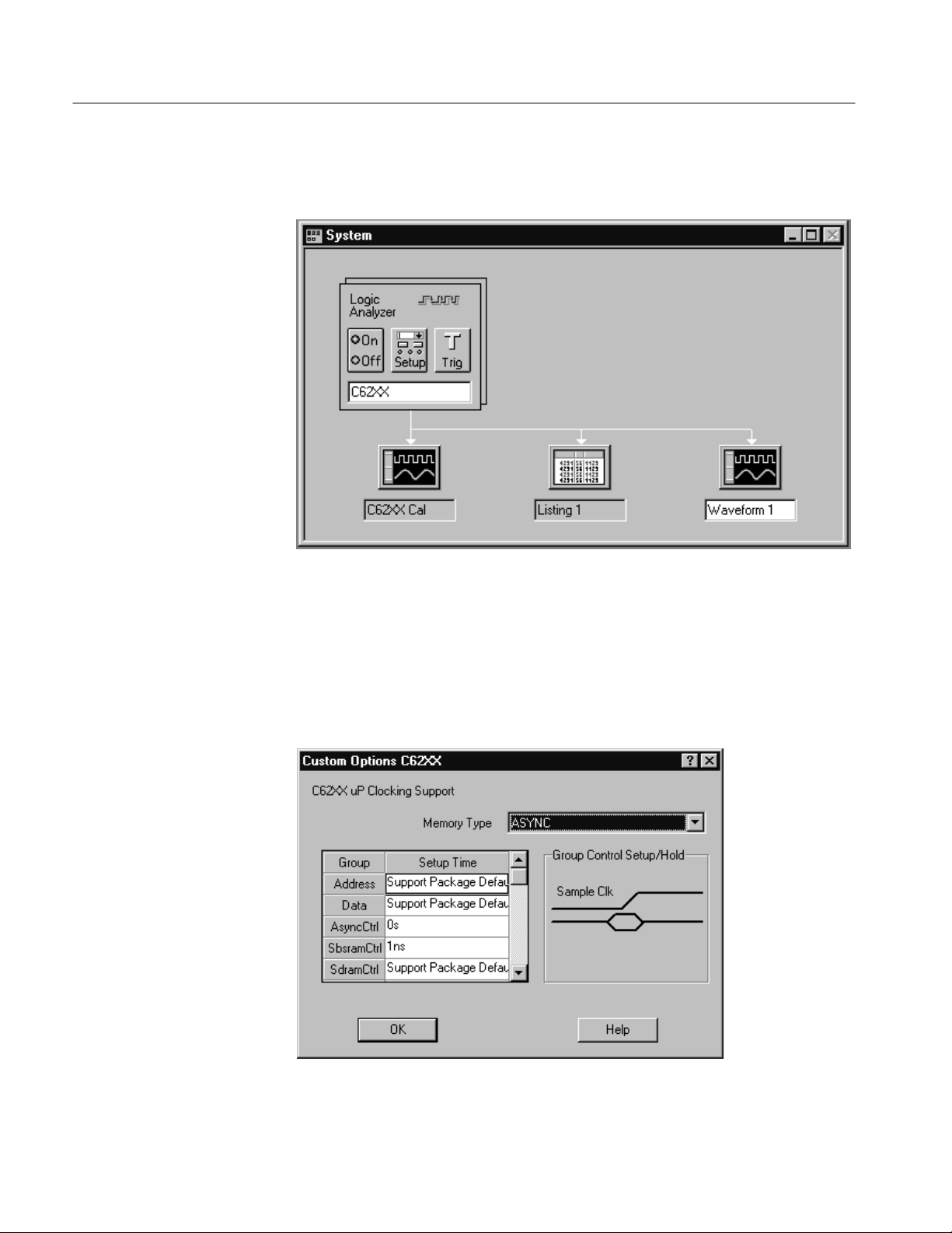
Figure 2–10 shows the Cal_Setup file loaded in the System window.
Figure 2–10: C6201 System window with the C6201 Cal Setup file
NOTE. For only SBSRAM memory calibration, go to step 10.
5. To enter the setup time values from the Setup: C62XX dialog box click the
More button to the right of the Custom Clocking field. A Custom Options
C62XX dialog box appears (see Figure 2–11). Select ASYNC in the Memory
Type field. The logic analyzer must trigger on the falling edge of ARE*.
2–12
TMS 710 TMS320C6201/C6701 Microprocessor Support
Page 47

Figure 2–11: C6201 Custom options C6201 dialog box
Setting Up the Support
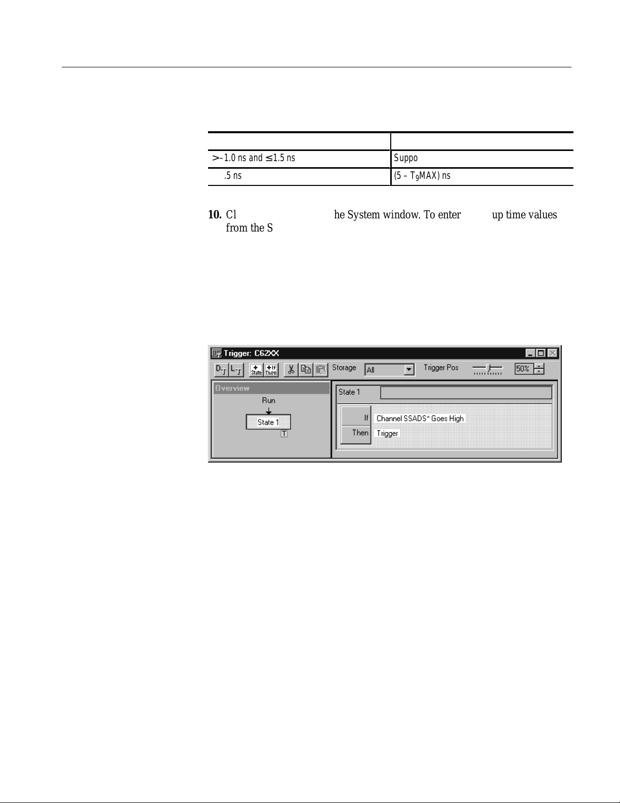
6. Click the Trigger icon in the System window. The Trigger: C62XX dialog
box appears with a predefined trigger. Figure 2–12 shows the setup to trigger.
Figure 2–12: C6201 Trigger setup for any asynchronous memory Read
7. With the system under test running, click the RUN button to acquire data.
After triggering, select the C6201 Cal Waveform Window.
TMS 710 TMS320C6201/C6701 Microprocessor Support
2–13
Page 48

Setting Up the Support
CLKOUT1
CEx
BE [3:0]
ED [21:2]
ED [31:0]
ASYNC Memory
Calibration
Setup = 2 Strobe = 5 Not ready = 2 Hold = 1
1
2
4
8. In Figure 2–13 the value of the timing parameter 9 is calculated from the
C6201 Cal Waveform Window for signals ARE*= and ARE* for both the
rising and falling edge. Parameter 9 is the Delay time from CLKOUT1 high
to a valid signal. The maximum (T
MAX) of the four calculated values is
9
taken to determine the setup value of the AsyncCtrl group as described in
Table 2–3. This procedure is useable if the difference between the maximum
and minimum calculated values are 2.5 ns or less.
1
3
5
6
7
8
AOE
9
ARE
AWE
11
10
ARDY
Data supplied by Texas Instruments, Inc.
11
10
Figure 2–13: C6201 Asynchronous memory read timing diagram
NOTE. For only asynchronous memory calibration, go to step 15.
9. In the Custom Options window, click on the setup time submenu of the
AsyncCtrl group. Select the setup time for the AsyncCtrl group as listed in
Table 2–3 from the calculated value of parameter 9 in Figure 2–13.
8
9
2–14
TMS 710 TMS320C6201/C6701 Microprocessor Support
Page 49
Setting Up the Support
T able 2–3: C6201 Setup time for the AsyncCtrl group
T9MAX Setup time used for AsyncCtrl group
> –1.0 ns and ≤ 1.5 ns
Support package Default
> 1.5 ns
(5 – T9MAX) ns
10. Click the Setup icon in the System window. To enter the setup time values
from the Setup: C6201 dialog box, click the More button to the right of the
Custom Clocking field. A Custom Options C6201 dialog box appears. In
Custom Option for SBSRAM memory calibration, select SBSRAM in the
memory type field. The logic analyzer must trigger on the raising edge of
SSADS*.
11. Click the Trigger icon in the System window. The Trigger: C62XX dialog
box appears with a predefined trigger. Figure 2–14 shows the setup to trigger.
Figure 2–14: C6201 Trigger setup for any SBSRAM memory Read
12. With the system under test running, click the RUN button to acquire data.
After triggering, select the C62XX Cal Waveform Window.
TMS 710 TMS320C6201/C6701 Microprocessor Support
2–15
Page 50

Setting Up the Support
SSCLK
CEx
BE [3:0]
EA [21:2]
ED [31:0]
SSADS
SSOE
SBSRAM Memory
Calibration
1
3
5
13. In Figure 2–15 the value of timing parameter 10 is calculated from the
C6201 Cal Waveform Window for signals SSADS* and SSADS*=. Both
values should fall within the range of this timing alignment procedure to be
useable. The Timing parameter 10 is the Output hold time for the signal that
is valid after SSCLK high.
2
4
BE1
A1
9
11
BE2 BE3 BE4
6
A2 A3 A4
8
7
Q1 Q2 Q3 Q4
10
12
SSWE
Data supplied by Texas Instruments, Inc.
Figure 2–15: C6201 SBSRAM memory read timing (full-rate SSCLK) diagram
14. In the Custom Options window click on the setup time submenu of the
SbsramCtrl group. Select the setup time for the SbsramCtrl group as listed in
Table 2–4 from the calculated value of parameter 10 in Figure 2–15.
T able 2–4: C6201 Setup time for the SbsramCtrl group
If the value of parameter 10 is:
< 1.5 ns
≥ 1.5 ns
15. Click the Setup icon in the System window. To enter the setup time values
from the Setup: C6201 dialog box, click the More button to the right of the
Custom Clocking field. A Custom Options C6201 dialog box appears.
Setup time used for SbsramCtrl group
Support package Default
1.0 ns
2–16
TMS 710 TMS320C6201/C6701 Microprocessor Support
Page 51

Setting Up the Support
16. Enter the values that you calculated in step 9 and 14 in the Setup time
column to the right of the AsyncCtrl channel group and SbsramCtrl channel
group respectively.
Figure 2–16 shows the Custom Options C62XX dialog box and the Setup time
column. The values that you enter in this column will be different.
Figure 2–16: C6201 Custom options C6201 dialog box
17. With the system under test running, click the RUN button to acquire data.
After triggering, select the Listing window.
Figure 2–25 on page 2–27 shows the valid disassembled data after aligning
the edges.
18. To save the setup time values to restore at a later time, select Save System
As ... from the File menu. If you do not change the system under test, you do
not need to recalculate these values.
If you want to save the setup only, make sure that the Save Acquired Data
box is clear (no check).
TMS 710 TMS320C6201/C6701 Microprocessor Support
2–17
Page 52

Setting Up the Support
Logic Analyzer Time Alignment for the C6701
The setup time alignment of the logic analyzer to a system under test may be
necessary if the C6701
in Table 2–5 with similar memory types. To ensure that the logic analyzer
acquires correct data at higher clock speeds, you may need to follow these
procedures and make the setup timing adjustments.
T able 2–5: C6701 Memory types and maximum frequencies
Memory type
microprocessor operates at a frequency greater than listed
TMS 710 C6701 supported
maximum frequencies
without alignment
C6701 maximum
Asynchronous
SBSRAM
SDRAM
115 MHz
167 MHz
167 MHz
167 MHz
167 MHz
167 MHz
For the Asynchronous memory, following steps 1 through 16 can increase the
supported maximum frequency. A setup time alignment procedure is not included
for the SDRAM and SBSRAM memories, since the memory operates at the
supported maximum frequency.
1. From the System window in the File menu, select Load System.
2. From the Load System dialog box, browse to where the Cal_Setup.tla file is
located. Figure 2–17 shows the Load System window with the Cal_Setup.tla
system setups.
2–18
Figure 2–17: C6701 Setup: Load System menu
TMS 710 TMS320C6201/C6701 Microprocessor Support
Page 53
Setting Up the Support
3. Select the Cal_Setup.tla file and click open. Click No in the caution dialog
box. If an Information dialog box appears, click OK.
The Load System Options dialog box may or may not appear.
4. If the Load System Options dialog box appears and the C62XX setup is not
loaded to the Current System, then drag the C62XX icon to the desired
module and click OK. If an information box appears click OK.
Figure 2–18 shows the Load System Options dialog box before dragging the
C62XX icon to the module in the Current System.
Figure 2–18: C6701 Load System Options dialog box
TMS 710 TMS320C6201/C6701 Microprocessor Support
2–19
Page 54
Setting Up the Support
Figure 2–19 shows the Cal_Setup file loaded in the System window.
Figure 2–19: C6701 System window with the Cal Setup file
5. To enter the setup time values from the Setup: C62XX dialog box click the
More button to the right of the Custom Clocking field. A Custom Options
C62XX dialog box appears (see Figure 2–20). Select ASYNC in the Memory
Type field. The logic analyzer must trigger on the falling edge of ARE*.
2–20
Figure 2–20: C6701 Custom options dialog box
TMS 710 TMS320C6201/C6701 Microprocessor Support
Page 55

Setting Up the Support
6. Click the Trigger icon in the System window. The Trigger: C62XX dialog
box appears with a predefined trigger. Figure 2–21 shows the setup to trigger.
Figure 2–21: C6701 Custom options dialog box
7. With the system under test running, click the RUN button to acquire data.
After triggering, select the C62XX Cal Waveform Window.
TMS 710 TMS320C6201/C6701 Microprocessor Support
2–21
Page 56
Setting Up the Support
CLKOUT1
CEx
BE [3:0]
ED [21:2]
ED [31:0]
ASYNC Memory
Calibration
Setup = 2 Strobe = 5 Not ready = 2 Hold = 1
1
2
4
8. In Figure 2–22, the value of the timing parameter 9 is calculated from the
C62XX Cal Waveform Window for signals ARE*= and ARE* for both the
rising and falling edge. Parameter 9 is the Delay time from CLKOUT1 high
to a valid signal. The maximum (T
MAX) of the four calculated values is
9
taken to determine the setup value of the AsyncCtrl group as described in
Table 2–3 on page 2–15. This procedure is useable if the difference between
the maximum and minimum calculated values are 2.5 ns or less.
1
3
5
6
7
8
AOE
9
ARE
AWE
11
10
ARDY
Data supplied by Texas Instruments, Inc.
11
10
Figure 2–22: C6701 Asynchronous memory read timing diagram
NOTE. For only asynchronous memory calibration, go to step 15.
9. In the Custom Options window, click on the setup time submenu of the
AsyncCtrl group. Select the setup time for the AsyncCtrl group as listed in
Table 2–6 from the calculated value of parameter 9 in Figure 2–22.
8
9
2–22
TMS 710 TMS320C6201/C6701 Microprocessor Support
Page 57

Setting Up the Support
T able 2–6: C6701 Setup time for the AsyncCtrl group
T9MAX Setup time used for AsyncCtrl group
> –1.0 ns and ≤ 1.5 ns
Support package Default
> 1.5 ns
(5 – T9MAX) ns
10. Click the Setup icon in the System window. To enter the setup time values
from the Setup: C6701 dialog box, click the More button to the right of the
Custom Clocking field. A Custom Options C6201 dialog box appears. In
Custom Option for SBSRAM memory calibration, select SBSRAM in the
memory type field. The logic analyzer must trigger on the raising edge of
SSADS*.
11. Click the Trigger icon in the System window. The Trigger: C62XX dialog
box appears with a predefined trigger. Figure 2–23 shows the setup to trigger.
Figure 2–23: C6701 Trigger setup for any SBSRAM memory Read
12. With the system under test running, click the RUN button to acquire data.
After triggering, select the C6201 Cal Waveform Window.
13. Click the Setup icon in the System window. To enter the setup time values
from the Setup: C6201 dialog box, click the More button to the right of the
Custom Clocking field. A Custom Options C6201 dialog box appears.
14. Enter the values that you calculated in step 9 in the Setup time column to the
right of the AsyncCtrl channel group.
TMS 710 TMS320C6201/C6701 Microprocessor Support
2–23
Page 58

Setting Up the Support
Figure 2–24 shows the Custom Options C6201 dialog box and the Setup time
column. The values that you enter in this column will be different.
Figure 2–24: C6701 Custom options dialog box
15. With the system under test running, click the RUN button to acquire data.
After triggering, select the Listing window.
Figure 2–25 on page 2–27 illustrates the valid disassembled data after
aligning the edges.
16. To save the setup time values to restore at a later time, select Save System
As ... from the File menu. If you do not change the system under test, you do
not need to recalculate these values.
If you want to save the setup only, make sure that the Save Acquired Data
box is clear (no check).
2–24
TMS 710 TMS320C6201/C6701 Microprocessor Support
Page 59

Acquiring and Viewing Disassembled Data
Acquiring Data
Once you load the C6201/C6701 support, choose a clocking mode, and specify
the trigger, you are ready to acquire and disassemble data.
If you have any problems acquiring data, refer to information on basic operations
in your online help or Appendix A: Error Messages and Disassembly Pr oblems in
the basic operations user manual.
Viewing Disassembled Data
You can view disassembled data in six display formats: Timing, State, Hardware,
Software, Control Flow, and Subroutine. The information on basic operations
describes how to select the disassembly display formats.
NOTE. Selections in the Disassembly property page (the Disassembly Format
Definition overlay) must be set correctly for your acquired data to be disassembled correctly. Refer to Changing How Data is Displayed on page 2–28.
The default display format displays the Address, Data, and Control channel
group values for each sample of acquired data.
If a channel group is not visible, you must use the Disassembly property page to
make the group visible.
The disassembler displays special characters and strings in the instruction
mnemonics to indicate significant events. Table 2–7 lists these special characters
and strings and gives a definition of what they represent.
T able 2–7: Description of special characters in the display
Character or string displayed Definition
>> The instruction was manually marked as a program fetch
****
#
t
Indicates there is insufficient data available for complete
disassembly of the instruction; the number of asterisks
indicates the width of the data that is unavailable. Every two
asterisks represent one byte.
Indicates an immediate value
Indicates the number shown is in decimal, such as #12t
TMS 710 TMS320C6201/C6701 Microprocessor Support
2–25
Page 60

Acquiring and Viewing Disassembled Data
Timing Display Format
The timing-waveform display format file is provided for the TLA 700 Series
support. The timing-waveform display format file will set up and display the
following waveforms:
CLKOUT1
Address (busform)
Data (busform)
RESET*
SDCLK
SDRAS*
SDCAS*
SDWE*
SSCLK
SSADS*
SSOE*
SSWE*
ARE*
AWE*
CE3*
CE2*
CE1*
CE0*
BE3*
BE2*
BE1*
BE0*
LENDIAN
State-Listing Display
Format
Hardware Display Format
2–26
In the State-Listing display format, bus cycles are displayed and not disassembled. The State-Listing display format is provided for the TLA 700 Series
support.
In Hardware display format, the disassembler displays certain cycle type labels in
parentheses. Table 2–8 lists cycle type labels and gives a definition of the cycle
they represent. Reads to interrupt and exception vectors will be labeled with the
vector name.
T able 2–8: Cycle type definitions
Cycle Type Definition
( RESET )
( ALT MASTER CYCLE )
( SBSRAM:DATA WRITE )
( SBSRAM:DATA READ )
Indicates RESET sequence
Indicates bus cycle of alternate master
Indicates data write operation on SBSRAM
Indicates a data read cycle
TMS 710 TMS320C6201/C6701 Microprocessor Support
Page 61

Acquiring and Viewing Disassembled Data
T able 2–8: Cycle type definitions (cont.)
Cycle Type Definition
( SBSRAM: ADDRESS )
( ASYNC:DATA WRITE ) Indicates data write operation on ASYNC
Indicates address for an SBSRAM access
( SDRAM: ROW ADDR )
( SDRAM: COL ADDR )
( SDRAM: DATA WRITE )
( SDRAM: DATA READ )
( FLUSH )
( EXTENSION )
( UNKNOWN )
Indicates row address for an SDRAM access
Indicates column address for an SDRAM access
Indicates data write operation on SDRAM
Indicates data read cycle
Indicates a cycle was fetched but not executed
Indicates an extension to a preceding instruction opcode
Indicates a combination of control bits is unexpected and/or
unrecognized
Figure 2–25 shows an example of a Hardware display.
Figure 2–25: Hardware display format
TMS 710 TMS320C6201/C6701 Microprocessor Support
2–27
Page 62

Acquiring and Viewing Disassembled Data
Software Display Format
Control Flow Display
Format
Subroutine Display
Format
The Software display format displays only the first fetch of executed instructions.
Flushed cycles and extensions are not shown, even though they are part of the
executed instruction. Read extensions will be used to disassemble the instruction,
but they will not be displayed as a separate cycle in the Software display format.
Data reads and writes are not displayed.
The Control Flow display format displays only the first fetch of instructions that
cause a branch in the addressing and special cycles to change the flow of control.
Instructions that generate a change in the flow of control in the C6201/C6701
microprocessor are as follows:
B IRP B disp B NRP B reg
The Subroutine display format displays only the first fetch of subroutine call and
return instructions. It will display conditional subroutine calls if they are
considered to be taken.
Instructions that generate a subroutine call or a return in the C6201/C6701
microprocessor are as follows:
B IRP B NRP
Changing How Data is Displayed
There are common fields and features that allow you to further modify displayed
data to suit your needs. You can make common and optional display selections in
the Disassembly property page (the Disassembly Format Definition overlay).
Optional Display
Selections
You can make optional selections for acquired disassembled data. In addition to
the common selections (described in the information on basic operations), you
can change the displayed data in the following ways:
Show: Hardware (default)
Highlight: Software (default)
Disasm Across Gaps: Yes (default)
Software
Control Flow
Subroutine
Control Flow
Subroutine
None
No
2–28
TMS 710 TMS320C6201/C6701 Microprocessor Support
Page 63

Acquiring and Viewing Disassembled Data
Micro Specific Fields
Memory Map. When you use the Memory Map field you can select memory map
type C6201. The TMS 710 TMS320C6201/C6701support has two different
memory maps, MAP 0 and MAP 1. Default is Map 0.
The selections available are: MAP 0 (default)
MAP 1
Interrupt Table Base. When you use the Interrupt Table Base field you can enter
the base address of the Interrupt service table (IST). By default the Interrupt
Table Base field has 0x00000000 address. The specified address is on the 256
word boundary otherwise the TMS 710 TMS320C6201/C6701support changes
the address to the lower 256 word boundary.
CE1 Bus Width. When you use the CE1 Bus Width field, you can specify the bus
width of the memory in the CE1 space.
The selections available are: 8 Bit (default)
16 Bit
32 Bit
SDRAM Page Size. When you use the SDRAM Page Size field, you can specify
the SDRAM configuration on the system under test. You can refer to SDWID bit
setting in the EMIF SDRAM control register. If SDWID is 0, then 512 is
selected. If SDWID is 1, then option 256 is selected.
The selections available are: 512 Words (default)
256 Words
CE0 Memory T ype. When using the CE0 Memory Type field, you can specify the
type of memory located in the CE0 space.
The selections available are: ASYNC (default)
SBSRAM
SDRAM
CE1 Memory T ype. When using the CE1 Memory Type field, you can specify the
type of memory located in the CE1 space.
The selections available are: ASYNC (default)
SBSRAM
CE2 Memory T ype. When using the CE2 Memory Type field, you can specify the
type of memory located in the CE2 space.
TMS 710 TMS320C6201/C6701 Microprocessor Support
2–29
Page 64

Acquiring and Viewing Disassembled Data
The selections available are: ASYNC (default)
CE3 Memory T ype. When using the CE3 Memory Type field, you can specify the
type of memory located in the CE3 space.
The selections available are: ASYNC (default)
SBSRAM
SDRAM
SBSRAM
SDRAM
Marking Cycles
TMS 710 TMS320C6201/C6701support allows only the marking of instruction
The
fetch cycles (that includes read extensions and flush cycles). If the cursor is
placed on any other cycle type, no cycle marks will be available.
Marks are placed by using the Mark Opcode button. The Mark Opcode button
will always be available. If the sample being marked is not an Address cycle or
Data cycle of the potential bus master, the Mark Opcode selections will be
replaced by a note indicating that “An Opcode Mark cannot be placed at the
selected data sample.”
When a cycle is marked, this character >> is displayed immediately to the left of
the Mnemonics column. Cycles can be unmarked by using the Undo Mark
selection, which will remove this character >>.
The following cycle marks will be available for instruction fetch cycles:
H Opcode (the first word of an instruction)
H Flush (an opcode or extension that is fetched but not executed)
H Extension (mark a cycle as an extension to an instruction opcode)
H Undo Mark (remove all marks from the current sequence)
2–30
TMS 710 TMS320C6201/C6701 Microprocessor Support
Page 65

Acquiring and Viewing Disassembled Data
Displaying Exception
Vectors
The disassembler can display exception vectors.
You can relocate the table by entering the starting address in the Interrupt Table
Address field. The Interrupt Table Address field provides the disassembler with
the offset address; enter an eight-digit hexadecimal value corresponding to the
base address of the exception table.
You can make these selections in the Disassembly property page (the Disassembly Format Definition overlay).
Table 2–9 lists the
the C6201/C6701
TMS 710 TMS320C6201/C6701support exception vectors. See
microprocessor user manual for the meaning of these labels.
T able 2–9: Exception vectors
Location in interrupt
Exception
number
0 0000
1 0020
2 0080
3 00A0
4 00C0
5 00E0
6 0100
7 0120
8 0140
9 0160
10 0180
11 01A0
12 01C0
13 01E0
vector table
(in hexadecimal)
Displayed exception name
( RESET )
( NMI )
( INT4 )
( INT5 )
( INT6 )
( INT7 )
( INT8 )
( INT9 )
( INT10 )
( INT11 )
( INT12 )
( INT13 )
( INT14 )
( INT15 )
Viewing an Example of Disassembled Data
A demonstration system file (or demonstration reference memory) is provided so
you can see an example of how your C6201/C6701 microprocessor bus cycles
and instruction mnemonics look when they are disassembled. Viewing the system
file is not a requirement for preparing the module for use and you can view it
without connecting the logic analyzer to your system under test.
TMS 710 TMS320C6201/C6701 Microprocessor Support
2–31
Page 66

Acquiring and Viewing Disassembled Data
2–32
TMS 710 TMS320C6201/C6701 Microprocessor Support
Page 67

Specifications
Page 68

Page 69

Specifications
Specification Tables
This chapter contains information regarding the specifications of the
TMS 710 TMS320C6201/C6701
microprocessor support.
Tables 3–1 and 3–2 list the electrical requirements the system under test must
produce for the TMS 710 TMS320C6201/C6701 support to acquire correct data.
T able 3–1: C6201 Electrical specifications
Characteristics Requirements
System under test clock rate
Maximum specified clock rate:
ASYNC memory
SBSRAM memory
SDRAM memory
Tested clock rate 133 MHz
Minimum setup time required 2.5 ns
Minimum hold time required 0 ns
115 MHz
180 MHz
200 MHz
T able 3–2: C6701 Electrical Specifications
Characteristics Requirements
Sytem under test clock rate
Maximum specified clock rate:
ASYNC memory
SBSRAM memory
SDRAM memory
Tested clock rate
Minimum setup time required 2.5 ns
Minimum hold time required 0 ns
1
Please contact your Tektronix Sales Representative for current information on the
tested clock rate.
1
115 MHz
167 MHz
167 MHz
TMS 710 TMS320C6201/C6701 Microprocessor Support
3–1
Page 70

Specifications
3–2
TMS 710 TMS320C6201/C6701 Microprocessor Support
Page 71

Replaceable Parts
Page 72

Page 73

Replaceable Parts
This section contains a list of the replaceable parts for the
TMS 710 TMS320C6201/C6701 microprocessor support product.
Parts Ordering Information
Replacement parts are available through your local Tektronix field office or
representative.
Changes to Tektronix products are sometimes made to accommodate improved
components as they become available and to give you the benefit of the latest
improvements. Therefore, when ordering parts, it is important to include the
following information in your order.
H Part number
H Instrument type or model number
H Instrument serial number
H Instrument modification number, if applicable
Abbreviations
Mfr. Code to Manufacturer
Cross Index
If you order a part that has been replaced with a different or improved part, your
local Tektronix field office or representative will contact you concerning any
change in part number.
Abbreviations conform to American National Standard ANSI Y1.1–1972.
The table titled Manufacturers Cross Index shows codes, names, and addresses
of manufacturers or vendors of components listed in the parts list.
TMS 710 TMS320C6201/C6701 Microprocessor Support
4–1
Page 74

Replaceable Parts
Manufacturers cross index
Mfr.
code
TK2548 XEROX CORPORATION 14181 SW MILLIKAN WAY BEAVER T ON, OR 97005
Manufacturer Address City, state, zip code
Replaceable parts list
Fig. &
index
number
Tektronix
part number
071–0202–01 1 MANUAL, TECH: INSTRUCTIONS, C6201/C6701,
Serial no.
effective
Serial no.
discont’d
Qty Name & description Mfr. code Mfr. part number
STANDARD ACCESSORIES
TK2548 071–0202–01
TMS710
4–2
TMS 710 TMS320C6201/C6701 Microprocessor Support
Page 75

Index
Page 76

Page 77

Index
A
about this manual set, ix
acquiring data, 2–25
Address group, channel assignments, 1–4
application, logic analyzer configuration, 1–1
B
bus cycles, displayed cycle types, 2–26
bus speed, 1–2
Bus Width, 2–29
C
C6201 clock rate, SUT, 3–1
C6201 loading, 3–1
C6201 Time Alignment Procedure
ASYNC memory calibration, 2–16
SBSRAM Memory Calibration, 2–14
C6201 Time Alignment procedure, Async and
SBSRAM, 2–10
C6701 clock rate, SUT, 3–1
C6701 loading, 3–1
C6701 Time Alignment Procedure, SBSRAM Memory
Calibration, 2–22
C6701 Time Alignment procedure, Async and
SBSRAM, 2–18
CE0 Memory T ype, 2–29
CE1 Memory T ype, 2–29
CE2 Memory T ype, 2–29
CE3 Memory T ype, 2–30
channel assignments
Address group, 1–4
clocks, 1–9
Control group, 1–7, 1–8
Data group, 1–5
DataSize group, 1–8
Misc group, 1–6, 1–7, 1–8, 1–9
channel groups, 2–1
visibility , 2–25
clock channel assignments, 1–9
clock rate, 1–2
SUT, 1–2
clocking, Custom, 2–1
clocking options, memory types, TLA 700 Series, 2–1
connections
CPU to Mictor, 1–10
no probe adapter, 1–3
channel probes, 1–4
contacting T ektronix, x
Control Flow display format, 2–28
Control group
channel assignments, 1–7, 1–8
symbol table, 2–9
CPU to Mictor connections, 1–10
Custom clocking, 2–1
cycle types, 2–26
D
data
acquiring, 2–25
disassembly formats
Control Flow, 2–28
Hardware, 2–26
Software, 2–28
Subroutine, 2–28
disassemlby formats
State-Listing, 2–26
Timing-Display, 2–26
data display , changing, 2–28
Data group, channel assignments, 1–5
DataSize group, channel assignments, 1–8
definitions
disassembler, ix
information on basic operations, ix
demonstration file, 2–31
disassembled data
cycle type definitions, 2–26
viewing, 2–25
viewing an example, 2–31
disassembler
definition, ix
logic analyzer configuration, 1–1
setup, 2–1
Disassembly Format Definition overlay, 2–28
Disassembly property page, 2–28
display formats
Control Flow, 2–28
Hardware, 2–26
Software, 2–28
special characters, 2–25
State-Listing, 2–26
Subroutine, 2–28
Timing-Display, 2–26
TMS 710 TMS320C6201/C6701 Microprocessor Support
Index–1
Page 78

Index
E
electrical specifications, 3–1
C6201, 3–1
C6201 clock rate, 3–1
C6701 clock rate, 3–1
C6701 loading, 3–1
clock rate, 1–2
exception vectors, 2–31
H
Hardware display format, 2–26
cycle type definitions, 2–26
hold time, minimum, 3–1
I
Interrupt Table Base, 2–29
L
logic analyzer
configuration for disassembler, 1–1
configuration for the application, 1–1
software compatibility, 1–1
M
manual
conventions, ix
how to use the set, ix
Mark Cycle function, 2–30
Mark Opcode function, 2–30
marking cycles, definition of, 2–30
Memory Maps, 2–29
Micro Specific Fields
Bus Width, 2–29
CE0 Memory T ype, 2–29
CE1 Memory T ype, 2–29
CE2 Memory T ype, 2–29
CE3 Memory T ype, 2–30
Interrupt table Base, 2–29
Memory Maps, 2–29
SDRAM Page Size, 2–29
Mictor to CPU connections, 1–10
Misc group, channel assignments, 1–6, 1–7, 1–8, 1–9
Module Compatibility specifications, bus speed, 1–2
MTIF probes, 1–3
P
probe adapter, not using one, 1–3
R
reference memory, 2–31
restrictions, 1–2
without a probe adapter, 1–3
S
SDRAM Page Size, 2–29
set up time, minimum, 3–1
setups
disassembler, 2–1
support, 2–1
Software display format, 2–28
special characters displayed, 2–25
specifications, 3–1
channel assignments, 1–4
electrical, 3–1
State-Listing display format, 2–26
Subroutine display format, 2–28
support, setup, 2–1
support setup, 2–1
symbol table, Control channel group, 2–9
system file, demonstration, 2–31
T
T ektronix, how to contact, x
terminology, ix
Timing-Display format, 2–26
V
viewing disassembled data, 2–25
Index–2
TMS 710 TMS320C6201/C6701 Microprocessor Support
 Loading...