

Page 1

Instruction Manual
TMS 702
TMS320C3X Digital Signal Processor Support
070-9831-00
There are no current European directives that
apply to this product. This product provides
cable and test lead connections to a test object of
electronic measuring and test equipment.
Warning
The servicing instructions are for use by
qualified personnel only. To avoid personal
injury, do not perform any servicing unless you
are qualified to do so. Refer to all safety
summaries prior to performing service.
Page 2

Copyright T ektronix, Inc. All rights reserved. Licensed software products are owned by Tektronix or its suppliers and are
protected by United States copyright laws and international treaty provisions.
Use, duplication, or disclosure by the Government is subject to restrictions as set forth in subparagraph (c)(1)(ii) of the
Rights in T echnical Data and Computer Software clause at DFARS 252.227-7013, or subparagraphs (c)(1) and (2) of the
Commercial Computer Software – Restricted Rights clause at F AR 52.227-19, as applicable.
T ektronix products are covered by U.S. and foreign patents, issued and pending. Information in this publication supercedes
that in all previously published material. Specifications and price change privileges reserved.
Printed in the U.S.A.
T ektronix, Inc., P.O. Box 1000, Wilsonville, OR 97070–1000
TEKTRONIX and TEK are registered trademarks of T ektronix, Inc.
Page 3

SOFTWARE WARRANTY
T ektronix warrants that the media on which this software product is furnished and the encoding of the programs on
the media will be free from defects in materials and workmanship for a period of three (3) months from the date of
shipment. If a medium or encoding proves defective during the warranty period, T ektronix will provide a
replacement in exchange for the defective medium. Except as to the media on which this software product is
furnished, this software product is provided “as is” without warranty of any kind, either express or implied.
T ektronix does not warrant that the functions contained in this software product will meet Customer’s
requirements or that the operation of the programs will be uninterrupted or error-free.
In order to obtain service under this warranty, Customer must notify Tektronix of the defect before the expiration
of the warranty period. If T ektronix is unable to provide a replacement that is free from defects in materials and
workmanship within a reasonable time thereafter, Customer may terminate the license for this software product
and return this software product and any associated materials for credit or refund.
THIS WARRANTY IS GIVEN BY TEKTRONIX IN LIEU OF ANY OTHER WARRANTIES, EXPRESS
OR IMPLIED. TEKTRONIX AND ITS VENDORS DISCLAIM ANY IMPLIED WARRANTIES OF
MERCHANTABILITY OR FITNESS FOR A PARTICULAR PURPOSE. TEKTRONIX’
RESPONSIBILITY TO REPLACE DEFECTIVE MEDIA OR REFUND CUSTOMER’S PAYMENT IS
THE SOLE AND EXCLUSIVE REMEDY PROVIDED TO THE CUSTOMER FOR BREACH OF THIS
WARRANTY. TEKTRONIX AND ITS VENDORS WILL NOT BE LIABLE FOR ANY INDIRECT,
SPECIAL, INCIDENTAL, OR CONSEQUENTIAL DAMAGES IRRESPECTIVE OF WHETHER
TEKTRONIX OR THE VENDOR HAS ADVANCE NOTICE OF THE POSSIBILITY OF SUCH
DAMAGES.
Page 4

HARDWARE WARRANTY
T ektronix warrants that the products that it manufactures and sells will be free from defects in materials and
workmanship for a period of one (1) year from the date of shipment. If a product proves defective during this
warranty period, T ektronix, at its option, either will repair the defective product without charge for parts and labor,
or will provide a replacement in exchange for the defective product.
In order to obtain service under this warranty, Customer must notify Tektronix of the defect before the expiration
of the warranty period and make suitable arrangements for the performance of service. Customer shall be
responsible for packaging and shipping the defective product to the service center designated by T ektronix, with
shipping charges prepaid. Tektronix shall pay for the return of the product to Customer if the shipment is to a
location within the country in which the T ektronix service center is located. Customer shall be responsible for
paying all shipping charges, duties, taxes, and any other charges for products returned to any other locations.
This warranty shall not apply to any defect, failure or damage caused by improper use or improper or inadequate
maintenance and care. T ektronix shall not be obligated to furnish service under this warranty a) to repair damage
resulting from attempts by personnel other than T ektronix representatives to install, repair or service the product;
b) to repair damage resulting from improper use or connection to incompatible equipment; c) to repair any
damage or malfunction caused by the use of non-T ektronix supplies; or d) to service a product that has been
modified or integrated with other products when the effect of such modification or integration increases the time
or difficulty of servicing the product.
THIS WARRANTY IS GIVEN BY TEKTRONIX IN LIEU OF ANY OTHER WARRANTIES, EXPRESS
OR IMPLIED. TEKTRONIX AND ITS VENDORS DISCLAIM ANY IMPLIED WARRANTIES OF
MERCHANTABILITY OR FITNESS FOR A PARTICULAR PURPOSE. TEKTRONIX’
RESPONSIBILITY TO REPAIR OR REPLACE DEFECTIVE PRODUCTS IS THE SOLE AND
EXCLUSIVE REMEDY PROVIDED TO THE CUST OMER FOR BREACH OF THIS WARRANTY.
TEKTRONIX AND ITS VENDORS WILL NOT BE LIABLE FOR ANY INDIRECT , SPECIAL,
INCIDENTAL, OR CONSEQUENTIAL DAMAGES IRRESPECTIVE OF WHETHER TEKTRONIX OR
THE VENDOR HAS ADVANCE NOTICE OF THE POSSIBILITY OF SUCH DAMAGES.
Page 5

Table of Contents
Getting Started
Operating Basics
General Safety Summary v. . . . . . . . . . . . . . . . . . . . . . . . . . . . . . . . . . . . . . . . . . .
Service Safety Summary vii. . . . . . . . . . . . . . . . . . . . . . . . . . . . . . . . . . . . . . . . . . .
Preface: Digital Signal Processor Support Documentation ix. . . . . . . . .
Manual Conventions ix. . . . . . . . . . . . . . . . . . . . . . . . . . . . . . . . . . . . . . . . . . . . . .
Logic Analyzer Documentation x. . . . . . . . . . . . . . . . . . . . . . . . . . . . . . . . . . . . . .
Contacting T ektronix x. . . . . . . . . . . . . . . . . . . . . . . . . . . . . . . . . . . . . . . . . . . . . .
Support Description 1–1. . . . . . . . . . . . . . . . . . . . . . . . . . . . . . . . . . . . . . . . . . . . . . .
Logic Analyzer Software Compatibility 1–2. . . . . . . . . . . . . . . . . . . . . . . . . . . . . . .
Logic Analyzer Configuration 1–2. . . . . . . . . . . . . . . . . . . . . . . . . . . . . . . . . . . . . . .
Requirements and Restrictions 1–2. . . . . . . . . . . . . . . . . . . . . . . . . . . . . . . . . . . . . . .
Configuring the Probe Adapter 1–3. . . . . . . . . . . . . . . . . . . . . . . . . . . . . . . . . . . . . .
Connecting to a System Under T est 1–3. . . . . . . . . . . . . . . . . . . . . . . . . . . . . . . . . . .
PGA Probe Adapter 1–4. . . . . . . . . . . . . . . . . . . . . . . . . . . . . . . . . . . . . . . . . . .
PQFP Probe Adapter 1–7. . . . . . . . . . . . . . . . . . . . . . . . . . . . . . . . . . . . . . . . . . .
Without a Probe Adapter 1–10. . . . . . . . . . . . . . . . . . . . . . . . . . . . . . . . . . . . . . . .
Setting Up the Support 2–1. . . . . . . . . . . . . . . . . . . . . . . . . . . . . . . . . . . . . .
Channel Group Definitions 2–1. . . . . . . . . . . . . . . . . . . . . . . . . . . . . . . . . . . . . . . . .
Clocking Options 2–1. . . . . . . . . . . . . . . . . . . . . . . . . . . . . . . . . . . . . . . . . . . . . . . . .
Wait State Mode 2–2. . . . . . . . . . . . . . . . . . . . . . . . . . . . . . . . . . . . . . . . . . . . . .
Num of SW Wait 2–2. . . . . . . . . . . . . . . . . . . . . . . . . . . . . . . . . . . . . . . . . . . . . .
Alternate Bus Master (ABM) Cycles 2–2. . . . . . . . . . . . . . . . . . . . . . . . . . . . . .
Symbols 2–3. . . . . . . . . . . . . . . . . . . . . . . . . . . . . . . . . . . . . . . . . . . . . . . . . . . . . . . .
Triggering 2–4. . . . . . . . . . . . . . . . . . . . . . . . . . . . . . . . . . . . . . . . . . . . . . . . . . . . . . .
Triggering on the Expansion Address Bus 2–4. . . . . . . . . . . . . . . . . . . . . . . . . .
Acquiring and Viewing Disassembled Data 2–5. . . . . . . . . . . . . . . . . . . . .
Acquiring Data 2–5. . . . . . . . . . . . . . . . . . . . . . . . . . . . . . . . . . . . . . . . . . . . . . . . . . .
Viewing Disassembled Data 2–5. . . . . . . . . . . . . . . . . . . . . . . . . . . . . . . . . . . . . . . .
Hardware Display Format 2–6. . . . . . . . . . . . . . . . . . . . . . . . . . . . . . . . . . . . . . .
Software Display Format 2–7. . . . . . . . . . . . . . . . . . . . . . . . . . . . . . . . . . . . . . .
Control Flow Display Format 2–8. . . . . . . . . . . . . . . . . . . . . . . . . . . . . . . . . . . .
Subroutine Display Format 2–8. . . . . . . . . . . . . . . . . . . . . . . . . . . . . . . . . . . . . .
Changing How Data is Displayed 2–8. . . . . . . . . . . . . . . . . . . . . . . . . . . . . . . . . . . .
Optional Display Selections 2–8. . . . . . . . . . . . . . . . . . . . . . . . . . . . . . . . . . . . .
Marking Cycles 2–9. . . . . . . . . . . . . . . . . . . . . . . . . . . . . . . . . . . . . . . . . . . . . . .
Viewing an Example of Disassembled Data 2–9. . . . . . . . . . . . . . . . . . . . . . . . . . . .
TMS 702 TMS320C3X Digital Signal Processor Support Instruction Manual
i
Page 6

Table of Contents
Specifications
Probe Adapter Description 3–1. . . . . . . . . . . . . . . . . . . . . . . . . . . . . . . . . . . . . . . . . .
Specifications 3–2. . . . . . . . . . . . . . . . . . . . . . . . . . . . . . . . . . . . . . . . . . . . . . . . . . . .
How Data is Acquired 3–13. . . . . . . . . . . . . . . . . . . . . . . . . . . . . . . . . . . . . . . . . . . . .
Custom Clocking 3–13. . . . . . . . . . . . . . . . . . . . . . . . . . . . . . . . . . . . . . . . . . . . .
Clocking Options 3–14. . . . . . . . . . . . . . . . . . . . . . . . . . . . . . . . . . . . . . . . . . . . .
Alternate Microprocessor Connections 3–15. . . . . . . . . . . . . . . . . . . . . . . . . . . . . . . .
Signals Not On the Probe Adapter 3–15. . . . . . . . . . . . . . . . . . . . . . . . . . . . . . . .
Extra Channels 3–16. . . . . . . . . . . . . . . . . . . . . . . . . . . . . . . . . . . . . . . . . . . . . . .
Maintenance
Probe Adapter Circuit Description 4–1. . . . . . . . . . . . . . . . . . . . . . . . . . . . . . . . . . . .
Replacing Signal Leads 4–1. . . . . . . . . . . . . . . . . . . . . . . . . . . . . . . . . . . . . . . . . . . .
Replacing Protective Sockets 4–1. . . . . . . . . . . . . . . . . . . . . . . . . . . . . . . . . . . . . . . .
Replaceable Electrical Parts
Parts Ordering Information 5–1. . . . . . . . . . . . . . . . . . . . . . . . . . . . . . . . . . . . . . . . .
Using the Replaceable Electrical Parts List 5–1. . . . . . . . . . . . . . . . . . . . . . . . . . . . .
Replaceable Mechanical Parts
Parts Ordering Information 6–1. . . . . . . . . . . . . . . . . . . . . . . . . . . . . . . . . . . . . . . . .
Using the Replaceable Mechanical Parts List 6–1. . . . . . . . . . . . . . . . . . . . . . . . . . .
Index
Index Index–1. . . . . . . . . . . . . . . . . . . . . . . . . . . . . . . . . . . . . . . . . . . . . . . . . . . . . . . . . . .
ii
TMS 702 TMS320C3X Digital Signal Processor Support Instruction Manual
Page 7

List of Figures
Table of Contents
Figure 1–1: Placing the processor into a PGA probe adapter 1–5. . . . . . .
Figure 1–2: Connecting probes to a PGA probe adapter 1–6. . . . . . . . . .
Figure 1–3: Placing a PGA probe adapter onto the SUT 1–7. . . . . . . . . .
Figure 1–4: Connecting probes to a PQFP probe adapter 1–8. . . . . . . . .
Figure 1–5: Placing a PQFP probe adapter onto the SUT 1–10. . . . . . . . .
Figure 2–1: Hardware display format 2–7. . . . . . . . . . . . . . . . . . . . . . . . . .
Figure 3–1: Dimensions of the PGA probe adapter 3–4. . . . . . . . . . . . . . .
Figure 3–2: Dimensions of the PQFP probe adapter 3–5. . . . . . . . . . . . . .
Figure 3–3: TMS320C3X Primary and Expansion bus timing 3–13. . . . . .
Figure 3–4: TMS320C3X Expansion bus timing 3–14. . . . . . . . . . . . . . . . .
TMS 702 TMS320C3X Digital Signal Processor Support Instruction Manual
iii
Page 8

Table of Contents
List of Tables
Table 1–1: Supported digital signal processors 1–1. . . . . . . . . . . . . . . . . .
Table 1–2: Disassembly and Timing jumper information 1–3. . . . . . . . .
Table 1–3: TMS320C3X Primary bus signal connections for
channel probes 1–11. . . . . . . . . . . . . . . . . . . . . . . . . . . . . . . . . . . . . . . . .
Table 1–4: TMS320C3X Expansion bus signal connections for
channel probes 1–13. . . . . . . . . . . . . . . . . . . . . . . . . . . . . . . . . . . . . . . . .
Table 1–5: Clock channel assignments 1–14. . . . . . . . . . . . . . . . . . . . . . . . .
Table 2–1: Control group symbol table definitions 2–3. . . . . . . . . . . . . . .
Table 2–2: Meaning of special characters in the display 2–6. . . . . . . . . .
Table 2–3: Cycle type definitions 2–6. . . . . . . . . . . . . . . . . . . . . . . . . . . . .
Table 3–1: Jumper positions and function 3–1. . . . . . . . . . . . . . . . . . . . . .
Table 3–2: Electrical specifications 3–2. . . . . . . . . . . . . . . . . . . . . . . . . . . .
Table 3–3: Environmental specifications 3–3. . . . . . . . . . . . . . . . . . . . . . .
Table 3–4: Certifications and compliances 3–3. . . . . . . . . . . . . . . . . . . . . .
Table 3–5: Primary bus Address group
channel assignments 3–6. . . . . . . . . . . . . . . . . . . . . . . . . . . . . . . . . . . . .
Table 3–6: Expansion bus Address group
channel assignments 3–7. . . . . . . . . . . . . . . . . . . . . . . . . . . . . . . . . . . . .
Table 3–7: Primary bus Data group
channel assignments 3–8. . . . . . . . . . . . . . . . . . . . . . . . . . . . . . . . . . . . .
Table 3–8: Expansion bus Data group
channel assignments 3–9. . . . . . . . . . . . . . . . . . . . . . . . . . . . . . . . . . . . .
Table 3–9: Primary bus Control group
channel assignments 3–10. . . . . . . . . . . . . . . . . . . . . . . . . . . . . . . . . . . . .
Table 3–10: Expansion bus Control group
channel assignments 3–11. . . . . . . . . . . . . . . . . . . . . . . . . . . . . . . . . . . . .
Table 3–11: Intr group channel assignments 3–11. . . . . . . . . . . . . . . . . . . .
Table 3–12: Misc group channel assignments 3–11. . . . . . . . . . . . . . . . . . .
Table 3–13: Emulatn group channel assignments 3–12. . . . . . . . . . . . . . . .
Table 3–14: Clock channel assignments 3–12. . . . . . . . . . . . . . . . . . . . . . . .
Table 3–15: Extra module sections and channels 3–16. . . . . . . . . . . . . . . .
iv
TMS 702 TMS320C3X Digital Signal Processor Support Instruction Manual
Page 9

General Safety Summary
Review the following safety precautions to avoid injury and prevent damage to
this product or any products connected to it. To avoid potential hazards, use this
product only as specified.
Only qualified personnel should perform service procedures.
While using this product, you may need to access other parts of the system. Read
the General Safety Summary in other system manuals for warnings and cautions
related to operating the system.
To Avoid Fire or
Personal Injury
Connect and Disconnect Properly . Do not connect or disconnect probes or test
leads while they are connected to a voltage source.
Observe All Terminal Ratings. To avoid fire or shock hazard, observe all ratings
and marking on the product. Consult the product manual for further ratings
information before making connections to the product.
Do not apply a potential to any terminal, including the common terminal, that
exceeds the maximum rating of that terminal.
Avoid Exposed Circuitry. Do not touch exposed connections and components
when power is present.
Do Not Operate With Suspected Failures. If you suspect there is damage to this
product, have it inspected by qualified service personnel.
Do Not Operate in Wet/Damp Conditions.
Do Not Operate in an Explosive Atmosphere.
Keep Product Surfaces Clean and Dry .
Provide Proper Ventilation. Refer to the manual’s installation instructions for
details on installing the product so it has proper ventilation.
TMS 702 TMS320C3X Digital Signal Processor Support Instruction Manual
v
Page 10

General Safety Summary
Symbols and Terms
T erms in this Manual. These terms may appear in this manual:
WARNING. Warning statements identify conditions or practices that could result
in injury or loss of life.
CAUTION. Caution statements identify conditions or practices that could result in
damage to this product or other property.
T erms on the Product. These terms may appear on the product:
DANGER indicates an injury hazard immediately accessible as you read the
marking.
WARNING indicates an injury hazard not immediately accessible as you read the
marking.
CAUTION indicates a hazard to property including the product.
Symbols on the Product. The following symbols may appear on the product:
WARNING
High Voltage
Protective Ground
(Earth) T erminal
CAUTION
Refer to Manual
Double
Insulated
vi
TMS 702 TMS320C3X Digital Signal Processor Support Instruction Manual
Page 11

Service Safety Summary
Only qualified personnel should perform service procedures. Read this Service
Safety Summary and the General Safety Summary before performing any service
procedures.
Do Not Service Alone. Do not perform internal service or adjustments of this
product unless another person capable of rendering first aid and resuscitation is
present.
Disconnect Power. To avoid electric shock, disconnect the main power by means
of the power cord or, if provided, the power switch.
Use Care When Servicing With Power On. Dangerous voltages or currents may
exist in this product. Disconnect power, remove battery (if applicable), and
disconnect test leads before removing protective panels, soldering, or replacing
components.
To avoid electric shock, do not touch exposed connections.
TMS 702 TMS320C3X Digital Signal Processor Support Instruction Manual
vii
Page 12

Preface: Digital Signal Processor Support Documentation
This instruction manual contains specific information about the TMS 702
TMS320C3X digital signal processor support package and is part of a set of
information on how to operate this product on compatible Tektronix logic
analyzers.
If you are familiar with operating digital signal processor support packages on
the logic analyzer for which the TMS 702 TMS320C3X support was purchased,
you will probably only need this instruction manual to set up and run the support.
If you are not familiar with operating digital signal processor support packages,
you will need to supplement this instruction manual with information on basic
operations to set up and run the support.
Information on basic operations of digital signal processor support packages is
included with each product. Each logic analyzer has basic information that
describes how to perform tasks common to support packages on that platform.
This information can be in the form of online help, an installation manual, or a
user manual.
This manual provides detailed information on the following topics:
Manual Conventions
H Connecting the logic analyzer to the system under test
H Setting up the logic analyzer to acquire data from the system under test
H Acquiring and viewing disassembled data
H Using the probe adapter
This manual uses the following conventions:
H The term disassembler refers to the software that disassembles bus cycles
into instruction mnemonics and cycle types.
H The phrase “information on basic operations” refers to online help, an
installation manual, or a basic operations of digital signal processor supports
user manual.
H The term SUT (System Under Test) refers to the digital signal processor-
based system from which data will be acquired.
H The term Processor refers to the TMS320C3X digital signal processor.
TMS 702 TMS320C3X Digital Signal Processor Support Instruction Manual
ix
Page 13

Preface: Digital Signal Processor Support Documentation
H In the information on basic operations, the term XXX or P54C used in field
selections and file names must be replaced with processor. This is the name
of the digital signal processor in field selections and file names you must use
to operate the TMS320C3X support.
H The term logic analyzer refers to the Tektronix logic analyzer for which this
product was purchased.
H The term module refers to a 102/136-channel or a 96-channel module.
H processor refers to all supported variations of the TMS320C3X digital signal
processor unless otherwise noted.
H A tilde (~) following a signal name indicates an active low signal.
Logic Analyzer Documentation
A description of other documentation available for each type of Tektronix logic
analyzer is located in the corresponding module user manual. The manual set
provides the information necessary to install, operate, maintain, and service the
logic analyzer and associated products.
Contacting Tektronix
Product
Support
Service
Support
For other
information
To write us Tektronix, Inc.
For application-oriented questions about a Tektronix measurement product, call toll free in North America:
1-800-TEK-WIDE (1-800-835-9433 ext. 2400)
6:00 a.m. – 5:00 p.m. Pacific time
Or, contact us by e-mail:
tm_app_supp@tek.com
For product support outside of North America, contact your
local Tektronix distributor or sales office.
Contact your local Tektronix distributor or sales office. Or, visit
our web site for a listing of worldwide service locations.
http://www.tek.com
In North America:
1-800-TEK-WIDE (1-800-835-9433)
An operator will direct your call.
P.O. Box 1000
Wilsonville, OR 97070-1000
x
TMS 702 TMS320C3X Digital Signal Processor Support Instruction Manual
Page 14

Getting Started
Support Description
This chapter provides information on the following topics and tasks:
H A description of the TMS 702 digital signal processor support package
H Logic analyzer software compatibility
H Your System Under Test (SUT) requirements
H Support restrictions
H How to configure your probe adapter
H How to connect to your SUT
The TMS 702 digital signal processor support package disassembles data from
systems that are based on the Texas Instruments TMS320C3X digital signal
processor. The support runs on a compatible Tektronix logic analyzer equipped
with a 102/136-channel module or a 96-channel module.
Refer to information on basic operations to determine how many modules and
probes your logic analyzer needs to meet the minimum channel requirements for
the TMS 702 digital signal processor support.
Table 1–1 shows the digital signal processors and packages from which the
TMS 702 support can acquire and disassemble data.
T able 1–1: Supported digital signal processors
Name Package
TMS320C30 181-Pin PGA
TMS320C31 132-Pin PQFP
A complete list of standard and optional accessories is provided at the end of the
parts list in the Replaceable Mechanical Parts chapter.
A complete list of standard and optional accessories is provided at the end of the
parts list in the Replaceable Parts chapter.
To use this support efficiently, you need to have the items listed in the information on basic operations, as well as the TMS320C3X User’s Guide, Texas
Instruments Digital Signal Processing Products, June 1991.
TMS 702 TMS320C3X Digital Signal Processor Support Instruction Manual
1–1
Page 15

Getting Started
Information on basic operations also contains a general description of supports.
Logic Analyzer Software Compatibility
The label on the digital signal processor support floppy disk states which version
of logic analyzer software the support is compatible with.
Logic Analyzer Configuration
To use the TMS 702 support, the Tektronix logic analyzer must be equipped with
either a 102/136-channel module or a 96-channel module at a minimum. The
module must be equipped with enough probes to acquire channel and clock data
from signals in your TMS320C3X-based system.
Refer to information on basic operations to determine how many modules and
probes the logic analyzer needs to meet the channel requirements.
Requirements and Restrictions
You should review the general requirements and restrictions of digital signal
processor supports in the information on basic operations as they pertain to your
SUT.
You should review electrical, environmental, and mechanical specifications in the
Specifications chapter in this manual as they pertain to your SUT, as well as the
following descriptions of other TMS320C3X support requirements and restrictions.
System Clock Rate
TMS320C30 at speeds of up to 40 MHz, and the TMS320C31 at speeds of up to
33 MHz.
1
. The TMS 702 support can acquire data from the
1–2
1
Specification at time of printing. Contact your Tektronix sales representative for
current information on the fastest devices supported.
TMS 702 TMS320C3X Digital Signal Processor Support Instruction Manual
Page 16

Configuring the Probe Adapter
There is one jumper on the probe adapter used to configure the probe adapter for
disassembler analysis or timing analysis.
The Disassembly and Timing jumper (J120 on the PGA probe adapter, J520 on
the PQFP probe adapter) should be placed in the D position to acquire disassembled data, and in the T position to acquire timing data. Table 1–2 shows how
to position this jumper depending on the type of clocking you’re using and the
type of window you want to view.
T able 1–2: Disassembly and T iming jumper information
Jumper position Clocking Data window
D (Disassembly)
T (Timing) Internal Waveform window ,
Getting Started
Custom Listing window,
Disassembly, State, or
Graph displays
or Timing display
Connecting to a System Under Test
Before you connect to the SUT, you must connect the probes to the module.
Your SUT must also have a minimum amount of clear space surrounding the
processor to accommodate the probe adapter. Refer to the Specifications chapter
in this manual for the required clearances.
The channel and clock probes shown in this chapter are for a 102/136-channel
module. The probes will look different if you are using a 96-channel module.
The general requirements and restrictions of digital signal processor supports in
the information on basic operations shows the vertical dimensions of a channel or
clock probe connected to square pins on a circuit board.
TMS 702 TMS320C3X Digital Signal Processor Support Instruction Manual
1–3
Page 17

Getting Started
PGA Probe Adapter
To connect the logic analyzer to a SUT using a PGA probe adapter, follow these
steps:
1. Turn off power to your SUT. It is not necessary to turn off power to the logic
analyzer.
CAUTION. Static discharge can damage the processor the probe adapter, the
probes, or the module. To prevent static damage, handle all of the above only in a
static-free environment.
Always wear a grounding wrist strap or similar device while handling the
processor and probe adapter.
2. To discharge your stored static electricity, touch the ground connector located
on the back of the logic analyzer. Then, touch any of the ground pins of the
probe adapter to discharge stored static electricity from the probe adapter.
3. Place the probe adapter onto the antistatic shipping foam to support the probe
as shown in Figure 1–1. This prevents the circuit board from flexing and the
socket pins from bending.
4. Remove the processor from your SUT.
5. Line up the pin A1 indicator on the probe adapter board with the pin A1
indicator on the processor.
1–4
TMS 702 TMS320C3X Digital Signal Processor Support Instruction Manual
Page 18

6. Place the processor into the probe adapter as shown in
Figure 1–1.
Processor
Probe adapter
Foam
Getting Started
Figure 1–1: Placing the processor into a PGA probe adapter
CAUTION. Failure to correctly place the processor into the probe adapter may
permanently damage the processor once power is applied.
TMS 702 TMS320C3X Digital Signal Processor Support Instruction Manual
1–5
Page 19

Getting Started
7. Connect the channel and clock probes to the probe adapter as shown in
Figure 1–2. Match the channel groups and numbers on the probe labels to the
corresponding pins on the probe adapter. Match the ground pins on the
probes to the corresponding pins on the probe adapter.
Channel probe
and podlet holder
Hold the channel probes by the podlet
holder when connecting them to the
probe adapter. Do not hold them by
the cables or necks of the podlets.
Foam
Figure 1–2: Connecting probes to a PGA probe adapter
Clock probe
Probe adapter
1–6
8. Line up the pin A1 indicator on the probe adapter board with the pin A1
indicator on your SUT.
9. Place the probe adapter onto the SUT as shown in Figure 1–3.
NOTE. You might need to stack one or more replacement sockets between the SUT
and the probe adapter to provide sufficient vertical clearance from adjacent
components. However, keep in mind that this might increase loading, which can
reduce the electrical performance of your probe adapter.
TMS 702 TMS320C3X Digital Signal Processor Support Instruction Manual
Page 20

SUT socket
Getting Started
PQFP Probe Adapter
Figure 1–3: Placing a PGA probe adapter onto the SUT
To connect the logic analyzer to a SUT using a PQFP probe adapter, follow these
steps:
NOTE. The PQFP probe adapter connects to the primary bus only. There are no
connections to the expansion bus.
10. Turn off power to your SUT. It is not necessary to turn off the logic analyzer.
CAUTION. Static discharge can damage the processor, the probe adapter, the
probes, or the module. To prevent static damage, handle all the above only in a
static-free environment.
Always wear a grounding wrist strap or similar device while handling the
processor and probe adapter.
11. To discharge your stored static electricity, touch the ground connector located
on the back of the logic analyzer. Then, touch any of the ground pins of the
probe adapter to discharge stored static electricity from the probe adapter.
TMS 702 TMS320C3X Digital Signal Processor Support Instruction Manual
1–7
Page 21

Getting Started
12. Place the probe adapter onto the antistatic shipping foam to support the probe
as shown Figure 1–4. This prevents the circuit board from flexing.
13. Connect the channel and clock probes to the probe adapter as shown in
Figure 1–4. Match the channel groups and numbers on the probe labels to the
corresponding pins on the probe adapter. Match the ground pins on the
probes to the corresponding pins on the probe adapter.
Channel probe
and podlet holder
Hold the channel probes by the podlet
holder when connecting them to the
probe adapter. Do not hold them by
the cables or necks of the podlets.
Foam
Figure 1–4: Connecting probes to a PQFP probe adapter
Clock probe
Probe adapter
1–8
TMS 702 TMS320C3X Digital Signal Processor Support Instruction Manual
Page 22

Getting Started
CAUTION. This JEDEC
equipped with a clip that has been designed for tight tolerances.
The clip supports only Plastic Quad Flat Pack devices that conform to the
JEDEC M0-069 October 1990 specification. Attaching the clip to a device that
does not conform to this JEDEC standard can easily damage the clip’s connection pins and/or the processor, causing the probe adapter to malfunction.
Please contact your IC manufacturer to verify that the processor you are
targeting conforms to the JEDEC specification.
For best performance and long probe life, exercise extreme care when connecting
the probe to the processor.
14. Line up the pin 1 indicator on the processor with the pin 1 indicator on the
target head of the circuit board.
CAUTION. Failure to correctly place the probe adapter onto the processor might
permanently damage all electrical components when power is applied.
Center the clip on the processor and apply an equal downward force on all four
sides of the clip, slightly rocking the probe adapter in a clockwise circle.
PQFP (Plastic Quad Flat Pack) probe adapter has been
Do not apply leverage to the probe adapter when installing or removing it.
TMS 702 TMS320C3X Digital Signal Processor Support Instruction Manual
1–9
Page 23

Getting Started
15. Place the probe adapter onto the SUT as shown in Figure 1–5.
Without a Probe Adapter
Processor
Figure 1–5: Placing a PQFP probe adapter onto the SUT
CAUTION. The probe adapter board might slip off or slip to one side of the
processor because of the extra weight of the probes. This can damage the
processor and the SUT. To prevent this from occurring, stabilize the probe
adapter by placing a non-conductive object (such as foam) between the probe
adapter and the SUT.
You can use channel probes, clock probes, and leadsets with a commercial test
clip (or adapter) to make connections between the logic analyzer and your SUT.
To connect the probes to processor signals in the SUT using a test clip, follow
these steps:
1–10
16. Turn off power to your SUT. It is not necessary to turn off power to the logic
analyzer.
TMS 702 TMS320C3X Digital Signal Processor Support Instruction Manual
Page 24

Getting Started
CAUTION. Static discharge can damage the processor, the probes, or the module.
To prevent static damage, handle all of the above only in a static-free environment.
Always wear a grounding wrist strap or similar device while handling the
processor.
17. To discharge your stored static electricity, touch the ground connector located
on the back of the logic analyzer. If you are using a test clip, touch any of the
ground pins on the clip to discharge stored static electricity from it.
CAUTION. Failure to place the SUT on a horizontal surface before connecting the
test clip might permanently damage the pins on the processor.
18. Place the SUT on a horizontal static-free surface.
19. Use Table 1–3 to connect the channel probes to processor signal pins on the
test clip or in the SUT.
Use leadsets to connect at least one ground lead from each channel probe and
the ground lead from each clock probe to ground pins on your test clip.
Table 1–3 lists the primary bus signal connections for the channel probes.
T able 1–3: TMS320C3X Primary bus signal connections for channel probes
Section:channel TMS320C3X signal Section:channel TMS320C3X signal
A3:7 INT3~ * D3:7 D31
A3:6 INT2~ * D3:6 D30
A3:5 INT1~ * D3:5 D29
A3:4 INT0~ * D3:4 D28
A3:3 unused D3:3 D27
A3:2 HOLD~ * D3:2 D26
A3:1 H1 * D3:1 D25
A3:0 H3 * D3:0 D24
A2:7 A23 D2:7 D23
A2:6 A22 D2:6 D22
A2:5 A21 D2:5 D21
A2:4 A20 D2:4 D20
A2:3 A19 D2:3 D19
A2:2 A18 D2:2 D18
A2:1 A17 D2:1 D17
TMS 702 TMS320C3X Digital Signal Processor Support Instruction Manual
1–11
Page 25

Getting Started
T able 1–3: TMS320C3X Primary bus signal connections for channel probes (cont.)
Section:channel TMS320C3X signalSection:channelTMS320C3X signal
A2:0 A16 D2:0 D16
A1:7 A15 D1:7 D15
A1:6 A14 D1:6 D14
A1:5 A13 D1:5 D13
A1:4 A12 D1:4 D12
A1:3 A1 1 D1:3 D11
A1:2 A10 D1:2 D10
A1:1 A9 D1:1 D9
A1:0 A8 D1:0 D8
A0:7 A7 D0:7 D7
A0:6 A6 D0:6 D6
A0:5 A5 D0:5 D5
A0:4 A4 D0:4 D4
A0:3 A3 D0:3 D3
A0:2 A2 D0:2 D2
A0:1 A1 D0:1 D1
A0:0 A0 D0:0 D0
C3:7 EMU3 C2:7 MC/MP~ *
C3:6 EMU1 C2:6 R/W~
C3:5 EMU4/SHZ~ C2:5 RESET~
C3:4 EMU2 C2:4 RDY_D~ *
C3:3 EMU0 C2:3 STRB~
C3:2 XF1 * C2:2 IOSTRB~
C3:1 XF0 * C2:1 HOLDA~
C3:0 IACK~ C2:0 MSTRB~
C1:7 C0:7
C1:6 C0:6
C1:5 C0:5
C1:4 C0:4
C1:3 C0:3
C1:2 C0:2
C1:1 C0:1
C1:0 C0:0
* Signal not required for disassembly.
1–12
TMS 702 TMS320C3X Digital Signal Processor Support Instruction Manual
Page 26

Getting Started
Table 1–4 lists the expansion bus signal connections for the channel probes.
T able 1–4: TMS320C3X Expansion bus signal connections for channel
probes
Section:channel TMS320C3X signal Section:channel TMS320C3X signal
A3:7 XD3:7 XD31
A3:6 XD3:6 XD30
A3:5 XD3:5 XD29
A3:4 XD3:4 XD28
A3:3 XD3:3 XD27
A3:2 XD3:2 XD26
A3:1 XD3:1 XD25
A3:0 XD3:0 XD24
A2:7 XD2:7 XD23
A2:6 XD2:6 XD22
A2:5 XD2:5 XD21
A2:4 XD2:4 XD20
A2:3 XD2:3 XD19
A2:2 XD2:2 XD18
A2:1 XD2:1 XD17
A2:0 XD2:0 XD16
A1:7 XD1:7 XD15
A1:6 XD1:6 XD14
A1:5 XD1:5 XD13
XA1:4 XA12 XD1:4 XD12
XA1:3 XA1 1 XD1:3 XD11
XA1:2 XA10 XD1:2 XD10
XA1:1 XA9 XD1:1 XD9
XA1:0 XA8 XD1:0 XD8
XA0:7 XA7 XD0:7 XD7
XA0:6 XA6 XD0:6 XD6
XA0:5 XA5 XD0:5 XD5
XA0:4 XA4 XD0:4 XD4
XA0:3 XA3 XD0:3 XD3
XA0:2 XA2 XD0:2 XD2
XA0:1 XA1 XD0:1 XD1
XA0:0 XA0 XD0:0 XD0
TMS 702 TMS320C3X Digital Signal Processor Support Instruction Manual
1–13
Page 27
Getting Started
T able 1–4: TMS320C3X Expansion bus signal connections for channel
probes (cont.)
Section:channel TMS320C3X signalSection:channelTMS320C3X signal
C3:7 XC2:7 MC/MP~
C3:6 XC2:6 XR/W~
C3:5 XC2:5 RESET~
C3:4 XC2:4 XRDY_D~
C3:3 XC2:3 STRB~
C3:2 XC2:2 IOSTRB~
C3:1 XC2:1 HOLDA~
C3:0 XC2:0 MSTRB~
C1:7 C0:7
C1:6 C0:6
C1:5 C0:5
C1:4 C0:4
C1:3 C0:3
C1:2 C0:2
C1:1 C0:1
C1:0 C0:0
* Signal not required for disassembly.
1–14
Table 1–5 shows the clock probes and the processor signal to which they must
connect for disassembly to be correct.
T able 1–5: Clock channel assignments
Active
Clock channel Clock or Qualifier
Clock:2 Qualifier N/A RDY~ =
Clock:1 Qualifier N/A RESET~ =
Clock:0 Clock Both H1 =
XClock:2 Qualifier N/A XRDY~ =
XClock:1 Qualifier N/A RESET~ =
XClock:0 Clock Both H1 =
= Indicates the signal is doubled probed.
clock edge
TMS320C3X signal name
20. Align pin 1 or A1 of your test clip with the corresponding pin 1 or A1 of the
processor digital signal processor in your SUT and attach the clip.
TMS 702 TMS320C3X Digital Signal Processor Support Instruction Manual
Page 28

Setting Up the Support
This section provides information on how to set up the support. Information
covers the following topics:
H Channel group definitions
H Clocking options
H Symbol table files
Remember that the information in this section is specific to the operations and
functions of the TMS 702 TMS320C3X support on any Tektronix logic analyzer
for which it can be purchased. Information on basic operations describes general
tasks and functions.
Before you acquire and disassemble data, you need to load the support and
specify setups for clocking and triggering as described in the information on
basic operations. The support provides default values for each of these setups,
but you can change them as needed.
Channel Group Definitions
Clocking Options
The software automatically defines channel groups for the support. The channel
groups for the TMS320C3X support are Address, Data, and Control. If you want
to know which signal is in which group, refer to the channel assignment tables
beginning on page 3–6.
The TMS 702 support offers a digital signal processor-specific clocking mode for
the TMS320C3X processor. This clocking mode is the default selection
whenever you load the TMS320C3X support.
A description of how cycles are sampled by the module using the support and
probe adapter is found in the Specifications chapter.
Disassembly will not be correct with the Internal or External clocking modes.
Information on basic operations describes how to use these clock selections for
general purpose analysis.
The clocking options for the TMS 702 support are: Wait State Mode, Number of
SW Wait, and Alternate Bus Master Cycles.
TMS 702 TMS320C3X Digital Signal Processor Support Instruction Manual
2–1
Page 29

Setting Up the Support
Wait State Mode
The Wait State Mode field contains four selections that correspond to the
particular wait state mode you are using. The selections are Hardware Only,
Software Only, HW or SW, and HW and SW.
Hardware Only. This wait state depends only on the status of the external RDY~
line. The software wait state (SW Waits) are ignored.
Software Only . This wait state depends only on the number of SW Waits
programmed in the Num of SW Wait field. The status of the external RDY~ line
is ignored.
HW or SW. This wait state depends on either the status of the external RDY~ line,
or the number of SW Waits selected in the Num of SW Wait field, whichever
occurs earlier.
HW and SW. This wait state depends on both the status of the external RDY~ line
and the number of SW Waits selected in the Num of SW Wait field, whichever
occurs earlier. HW and SW is the default setting.
The TMS320C3X digital signal processors occasionally generate redundant read
or prefetch cycles when there is a contention for the internal pipeline resources or
external memory. The disassembly software identifies these redundant cycles and
flags them as “PIPELINE/MEMORY CONFLICT” cycles. Incorrect setting of
the “Wait State Mode” or the “Num of SW Wait” states fields can cause incorrect
disassembly.
Num of SW Wait
Alternate Bus Master
(ABM) Cycles
2–2
This field provides the number of SW Waits programed discussed under Wait
State Mode. This selection allows you to program the support to acquire correct
bus data when software-programmed wait-states are used. You enter the number
of wait states that the support is to insert in external cycles for the bus you are
monitoring. You can enter a value from zero to seven which will be used by the
Clocking State Machine (CSM) to track the completion of the bus cycle precisely
as the processor does. The default setting is zero (none). If the Wait State Mode
selected is HW Only, then the setting of this value does not matter.
The TMS 702 support has a select field with the label ABM Cycles. This field
has two selections, Excluded and Included.
Excluded. Alternate Bus Master (ABM) Cycles are not acquired or displayed.
Alternate Bus Master Cycles Excluded, is the default selection.
Included. All cycles are acquired.
TMS 702 TMS320C3X Digital Signal Processor Support Instruction Manual
Page 30

Symbols
Setting Up the Support
The TMS 702 support supplies one symbol table file. The processor_Ctrl file
replaces specific Control channel group values with symbolic values when
Symbolic is the radix for the channel group.
Table 2–1 shows the name, bit pattern, and meaning for the symbols in the file
processor_Ctrl, the Control channel group symbol table.
T able 2–1: Control group symbol table definitions
Control group value
RESET~ MSTRB~
Symbol
HOLDA~ IOSTRB~
IACK~ R/W~
STRB~
Meaning
XR/W~ mapped on to R/W~
XR/W~ mapped on to R/W~
XR/W~ mapped on to R/W~
XR/W~ mapped on to R/W~
XR/W~ mapped on to R/W~
XR/W~ mapped on to R/W~
Information on basic operations describes how to use symbolic values for
triggering and for displaying other channel groups symbolically, such as the
Address channel group.
TMS 702 TMS320C3X Digital Signal Processor Support Instruction Manual
2–3
Page 31

Setting Up the Support
Triggering
Triggering on the
Expansion Address Bus
The TMS320C3X expansion bus is 13-bits wide. The TMS320C3X probe
adapter ties the remaining most significant bits to ground. Therefore, when
entering values for the expansion address bus in the trigger menus, you must
enter those remaining bits as zeros. The disassembler synthesizes the upper bits
to match the memory map of the TMS320C3X data book.
You must also indicate either the MSTRB~ or the IOSTRB~ in the Control
section of the trigger menus. A convenient method would be to enter the symbols
provided by the TMS320C3X support.
2–4
TMS 702 TMS320C3X Digital Signal Processor Support Instruction Manual
Page 32

Acquiring and Viewing Disassembled Data
This section describes how to acquire data and view it disassembled. Information
covers the following topics and tasks:
H Acquiring data
H Viewing disassembled data in various display formats
H Cycle type labels
H Changing the way data is displayed
H Changing disassembled cycles with the mark cycles function
Acquiring Data
Once you load the TMS320C3X support, choose a clocking mode, and specify
the trigger, you are ready to acquire and disassemble
If you have any problems acquiring data, refer to information on basic operations
in your online help or Appendix A: Error Messages and Disassembly Problems in
the basic operations user manual.
data.
Viewing Disassembled Data
You can view disassembled data in four display formats: Hardware, Software,
Control Flow, and Subroutine. The information on basic operations describes
how to select the disassembly display formats.
NOTE. Selections in the Disassembly property page (the Disassembly Format
Definition overlay) must be set correctly for your acquired data to be disassembled correctly. Refer to Changing How Data is Displayed on page 2–8.
The default display format shows the Address, Data, and Control channel group
values for each sample of acquired data.
The disassembler displays special characters and strings in the instruction
mnemonics to indicate significant events. Table 2–2 shows these special
characters and strings, and gives a definition of what they represent.
TMS 702 TMS320C3X Digital Signal Processor Support Instruction Manual
2–5
Page 33

Acquiring and Viewing Disassembled Data
T able 2–2: Meaning of special characters in the display
Character or string displayed Meaning
or m
The instruction was manually marked
Hardware Display Format
****
Indicates there is insufficient data available for complete
disassembly of the instruction; the number of asterisks
indicates the width of the data that is unavailable. Each two
asterisks represent one byte.
In Hardware display format, the disassembler displays certain cycle-type labels
in parentheses. Table 2–3 shows these cycle type labels and gives a definition of
the cycle they represent. Reads to interrupt and exception vectors will be labeled
with the vector name.
T able 2–3: Cycle type definitions
Cycle type Definition
( FLUSH )
( PIPELINE/MEMORY CONFLICT ) [
( WRITE )
( READ )
( ACCESS_PRI )
( WRITE EXP )
( READ EXP )
A fetch cycle computed to be an opcode flush
The processor is rereading something
Write to the primary bus
Read from the primary bus
Primary bus access
Memory Write to the expansion bus
Memory Read from the expansion bus
2–6
( MEM_XP_BS )
( WR_I/O_XP )
( I/O_READ )
( I/O_WRITE )
( ALT BUS MSTR READ )
( ALT BUS MSTR WRITE )
( UNKNOWN )
[ The disassembler only does PIPELINE/MEMOR Y CONFLICT analysis on what the
disassembler determines as fetches. The disassembler will not do analysis on writes
or what the disassembler considers as non-fetch reads.
Memory access the expansion bus
I/O Write to the expansion bus
I/O Read from the expansion bus
I/O Write to the expansion bus
Alternate Bus Master Read cycle
Alternate Bus Master Write cycle
The combination of control bits is unexpected and/or
unrecoginized
TMS 702 TMS320C3X Digital Signal Processor Support Instruction Manual
Page 34

Acquiring and Viewing Disassembled Data
Figure 2–1 shows an example of the Hardware display.
1 2 3 4
Sample Address Data Mnemonics Timestamp
-------------------------------------------------------------------------------420 0001D8 0B62FFE8 NEGB FFE8,R2 70 ns
421 0001D9 17620018 SUBC 0018,R2 60 ns
422 0001DA 18E2000B SUBRB 000B,R2 70 ns
423 0001DB 08200100 LDI @000100,R0 70 ns
424 0001DC 1540C400 STI R0,*AR4 70 ns
425 000100 00400F04 ( READ ) 60 ns
426 0001DD 0C800000 NOP 70 ns
427 000000 00400F04 ( WRITE ) 130 ns
428 0001DE 0F200000 PUSH R0 140 ns
429 0001DF 0FA20000 PUSHF R2 60 ns
430 0001E0 0EA20000 POPF R2 70 ns
431 0001E1 0E200000 POP R0 70 ns
432 0001E2 0DC55811 NOT *--AR0(IR0),R5 60 ns
433 0001E3 0DC22101 NOT *AR1++(01),R2 70 ns
434 0001E4 0DC61102 NOT *++AR1(02),R6 70 ns
435 0001E5 62000291 CALL 000291 60 ns
436 0001E6 09412901 ( FLUSH ) 70 ns
437 000291 1A870007 ( READ ) 260 ns
438 000292 08670004 LDI 0004,R7 70 ns
439 000293 18670001 SUBI 0001,R7 70 ns
440 000294 6A06FFFE BNE 000293 70 ns
5
Software Display Format
Figure 2–1: Hardware display format
1
Sample Column. Lists the memory locations for the acquired data.
2
Address Group. Lists data from channels connected to the TMS320C3X
address bus.
3
Data Group. Lists data from channels connected to the TMS320C3X data
bus.
4
Mnemonics Column. Lists the disassembled instructions and cycle types.
5
Timestamp. Lists the timestamp values when a timestamp selection is made.
Information on basic operations describes how you can select a timestamp.
The Software display format shows only the first fetch of executed instructions.
Flushed cycles and extensions are not shown, even though they are part of the
executed instruction. Read extensions will be used to disassemble the instruction,
but will not be displayed as a separate cycle in the Software display format. Data
reads and writes are not displayed.
TMS 702 TMS320C3X Digital Signal Processor Support Instruction Manual
2–7
Page 35

Acquiring and Viewing Disassembled Data
Control Flow Display
Format
Subroutine Display
Format
The Control Flow display format shows only the first fetch of instructions that
change the flow of control.
Instructions that unconditionally generate a change in the flow of control in the
TMS320C3X digital signal processor are as follows:
BR BRD CALL
SWI RPTS RPTB
Instructions that conditionally generate a change in the flow of control in the
TMS320C3X digital signal processor are as follows:
Bcond BcondD CALLcond DBcond
DBcondD RETIcond RETScond TRAPcond
The Subroutine display format shows only the first fetch of subroutine call and
return instructions. It will display conditional subroutine calls if they are
considered to be taken.
Instructions that unconditionally generate a subroutine call or a return in the
TMS320C3X digital signal processor are as follows:
CALL SW1
Instructions that conditionally generate a subroutine call or a return in the
TMS320C3X digital signal processor are as follows:
CALLcond RETIcond RETScond TRAPcond
Changing How Data is Displayed
There are common fields and features that allow you to further modify displayed
data to suit your needs. You can make common and optional display selections in
the Disassembly property page (the Disassembly Format Definition overlay).
You can make selections unique to the TMS320C3X support to do the following
tasks:
H Change how data is displayed across all display formats
H Change the interpretation of disassembled cycles
Optional Display
Selections
You can make optional selections for disassembled
common selections (described in the information on basic operations), the
TMS320C3X support has one optional display selection, Data Page Pointer.
H Data page Pointer – Pointer to the page of data to be addressed in direct
addressing mode. All of the values displayed are displayed in hexadecimal.
data. In addition to the
2–8
TMS 702 TMS320C3X Digital Signal Processor Support Instruction Manual
Page 36

Acquiring and Viewing Disassembled Data
Marking Cycles
The disassembler has a Mark Opcode function that allows you to change the
interpretation of a cycle type. Using this function, you can select a cycle and
change it to one of the following cycle types:
H Opcode – the first word of an instruction
H Flush – an opcode or extension that is fetched but not executed
H Read – marks a memory reference read as data
H Undo Marks – Removes all marks from the current sequence
You can also use the Mark Opcode function to specify the default segment size
mode (16-bit or 32-bit) for the cycle. The segment size selection changes the
cycle the cursor is on and the remaining cycles to the end of memory or to the
next mark.
Information on basic operations contains more details on marking cycles.
Viewing an Example of Disassembled Data
A demonstration system file (or demonstration reference memory) is provided so
you can see an example of how your TMS320C3X digital signal processor bus
cycles and instruction mnemonics look when they are disassembled. Viewing the
system file is not a requirement for preparing the module for use and you can
view it without connecting the logic analyzer to your SUT.
Information on basic operations describes how to view the file.
TMS 702 TMS320C3X Digital Signal Processor Support Instruction Manual
2–9
Page 37

Specifications
J120 on the PGA probe
ter
J520 on the PQFP probe
ter
This chapter contains the following information:
H Probe adapter description
H Specification tables
H Dimensions of the probe adapter
H Channel assignment tables
H Description of how the module acquires processor signals
H List of other accessible TMS320C3X signals and extra probe channels
Probe Adapter Description
The probe adapter is nonintrusive hardware that allows the logic analyzer to
acquire data from a digital signal processor in its own operating environment
with little effect, if any, on that system. Information on basic operations contains
a figure showing the logic analyzer connected to a typical probe adapter. Refer to
that figure while reading the following description.
Configuration
The probe adapter consists of a circuit board and a socket for a TMS320C3X
processor. The probe adapter connects to the processor in the SUT. Signals from
the TMS320C3X-based system flow from the probe adapter to the channel
groups and through the probe signal leads to the module.
All circuitry on the probe adapter is powered from the SUT.
The probe adapter accommodates the Texas Instruments TMS320C3X digital
signal processor in a 181-pin PGA package, and in the 132-pin PQFP package.
Place the Disassembly and Timing jumper in the D position to acquire disassembled data, and in the T position to acquire timing data. Table 3–1 shows how
to position this jumper depending on the type of clocking you are using, and the
type of window you want to view.
T able 3–1: Jumper positions and function
Jumper Position Function
adap
,
D Use when acquiring disassembled data
adap
T Use when acquiring timing data
TMS 702 TMS320C3X Digital Signal Processor Support Instruction Manual
3–1
Page 38

Specifications
Specifications
These specifications are for a probe adapter connected between a compatible
Tektronix logic analyzer and a SUT. Table 3–2 shows the electrical requirements
the SUT must produce for the support to acquire correct data.
In Table 3–2, for the 102/136-channel module, one podlet load is 20 k in
parallel with 2 pF. For the 96-channel module, one podlet load is 100 k in
parallel with 10 pF.
T able 3–2: Electrical specifications
Characteristics Requirements
SUT DC power requirements
Voltage 4.75-5.25 VDC
Current I max (calculated) 16 mA
I max (measured) 3.5 mA
SUT clock
Clock rate Minimum 3.3 MHz
Maximum 33 MHz
Minimum setup time required 5 ns
Minimum hold time required 0 ns
Specification
Measured typical SUT signal loading
RESET~ 8 pF + 2 podlets 2 podlets
H1 6 pF + 2 podlets 2 podlets
MC/MP~ 6 pF + 1 podlet 1 podlet
R/W~, XR/W~ 4 to 7 pF + 2 podlets 2 podlets
STRB~, MSTRB~, IOSTRB~ 4 to 7 pF + 1 podlet 1 podlet
HOLDA~, IACK~ 4 to 7 pF + 1 podlet 1 podlet
RDY~, XRDY~ 4 to 7 pF + 1 U. L. 1 U. L.
All others 4 to 7 pF + 1 podlet 1 podlet
[
The AC loading capacitance includes run capacitance and the input capacitance of
the ICs.
AC load
[
DC load
3–2
TMS 702 TMS320C3X Digital Signal Processor Support Instruction Manual
Page 39
Table 3–3 shows the environmental specifications.
T able 3–3: Environmental specifications*
Characteristic Description
Temperature
Specifications
Maximum operating
Minimum operating 0° C (+32° F)
Non-operating –55° C to +75° C (–67° to +167° F)
Humidity 10 to 95% relative humidity
Altitude
Operating 4.5 km (15,000 ft) maximum
Non-operating 15 km (50,000 ft) maximum
Electrostatic immunity The probe adapter is static sensitive
* Designed to meet Tektronix standard 062-2847-00 class 5.
[
Not to exceed TMS320C3X digital signal processor thermal considerations. Forced air
cooling might be required across the CPU.
+50° C (+122° F)[
Table 3–4 shows the certifications and compliances that apply to the probe
adapter.
T able 3–4: Certifications and compliances
EC Compliance There are no current European Directives that apply to this product.
TMS 702 TMS320C3X Digital Signal Processor Support Instruction Manual
3–3
Page 40

Specifications
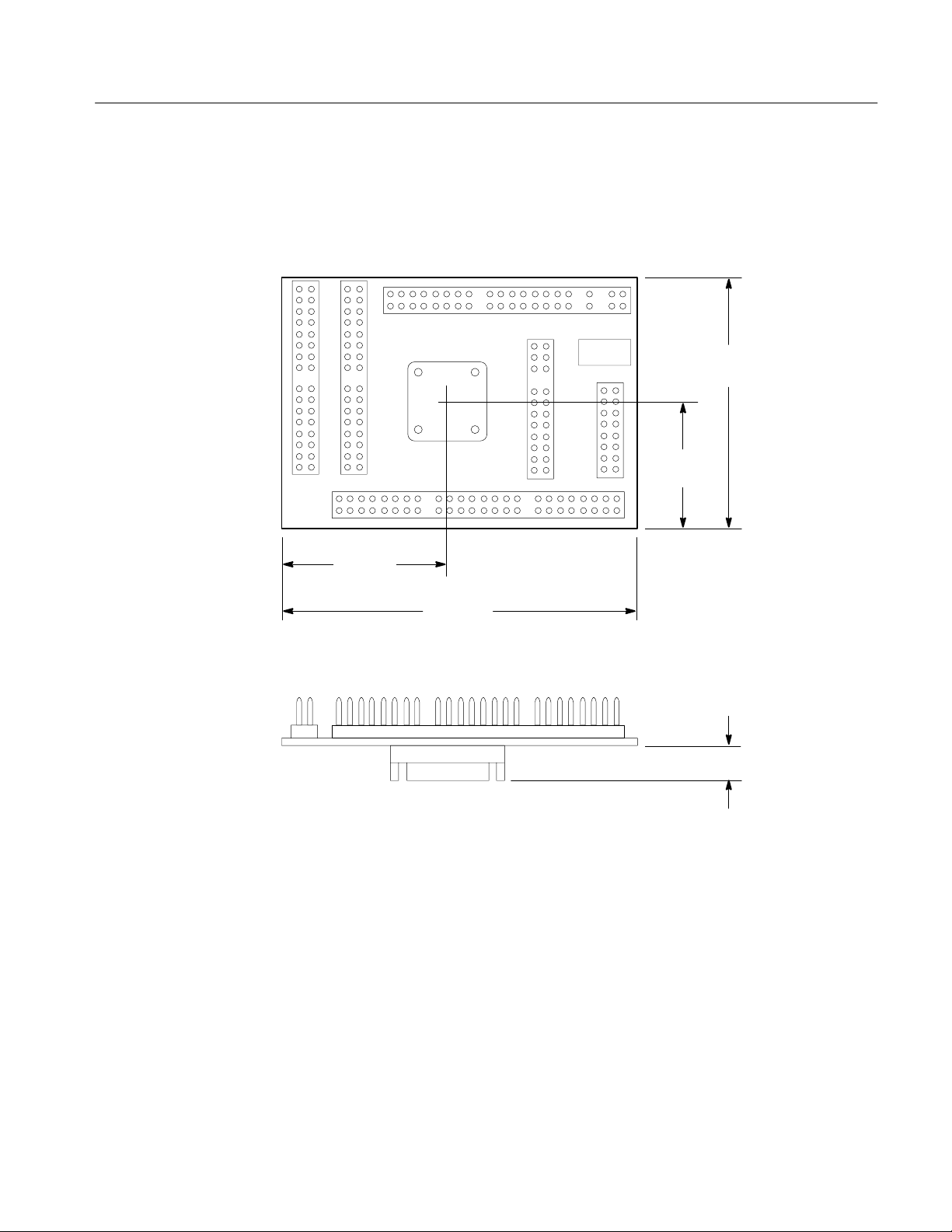
Figure 3–1 shows the dimensions of the PGA probe adapter. The figure also
shows the minimum vertical clearance of the high-density probe cable.
90 mm
(3.550 in)
90 mm
(3.550 in)
27 mm
(1.075 in)
27 mm
(1.075 in)
PIN A1
3–4
7 mm (.26 in)
Figure 3–1: Dimensions of the PGA probe adapter
TMS 702 TMS320C3X Digital Signal Processor Support Instruction Manual
Page 41
Specifications
Figure 3–2 shows the dimensions of the PQFP probe adapter. Information on
basic operations shows the vertical clearance of the channel and clock probes
when connected to a probe adapter.
57 mm
(2.225 in)
29 mm
(1.125 in)
43 mm
(1.700 in)
80 mm
(3.150 in)
Figure 3–2: Dimensions of the PQFP probe adapter
12 mm
(.46 in)
TMS 702 TMS320C3X Digital Signal Processor Support Instruction Manual
3–5
Page 42

Specifications
Channel Assignments
Channel assignments shown in Table 3–5 through Table 3–14 use the following
conventions:
H All signals are required by the support unless indicated otherwise.
H Channels are shown starting with the most significant bit (MSB) descending
to the least significant bit (LSB).
H Channel group assignments are for all modules unless otherwise noted.
H An tilde (~) following a signal name indicates that the signal is active low.
H An equals sign (=) following a signal name indicates that it is double probed.
H If there are two modules (such as used to form 96-channels), the module in
the higher-numbered slot is referred to as the HI module and the module in
the lower-numbered slot is referred to as the LO module.
Table 3–5 shows the probe section and channel assignments for the Primary bus
Address group and the TMS320C3X signal to which each channel connects. By
default, this channel group is displayed in hexadecimal.
T able 3–5: Primary bus Address group
channel assignments
Bit
order
23 A2:7 A23
22 A2:6 A22
21 A2:5 A21
20 A2:4 A20
19 A2:3 A19
18 A2:2 A18
17 A2:1 A17
16 A2:0 A16
15 A1:7 A15
14 A1:6 A14
13 A1:5 A13
12 A1:4 A12
11 A1:3 A11
10 A1:2 A10
9 A1:1 A9
8 A1:0 A8
7 A0:7 A7
6 A0:6 A6
Section:channel
TMS320C3X signal
name
3–6
TMS 702 TMS320C3X Digital Signal Processor Support Instruction Manual
Page 43

T able 3–5: Primary bus Address group
channel assignments (cont.)
Specifications
Bit
order
5 A0:5 A5
4 A0:4 A4
3 A0:3 A3
2 A0:2 A2
1 A0:1 A1
0 A0:0 A0
Section:channel
TMS320C3X signal
name
Table 3–6 shows the probe section and channel assignments for the Expansion
bus Address group and the TMS320C3X signal to which each channel connects.
By default, this channel group is displayed in hexadecimal.
The TMS320C3X Expansion address bus is 13-bits wide. Therefore, address pins
XA1:5 through XA1:7, and XA2:0 through XA2:7 on the probe adapter are tied
to ground.
T able 3–6: Expansion bus Address group
channel assignments
Bit
order
12 XA1:4 XA12
11 XA1:3 XA11
10 XA1:2 XA10
9 XA1:1 XA9
8 XA1:0 XA8
7 XA0:7 XA7
6 XA0:6 XA6
5 XA0:5 XA5
4 XA0:4 XA4
3 XA0:3 XA3
2 XA0:2 XA2
1 XA0:1 XA1
0 XA0:0 XA0
Section:channel
TMS320C3X signal
name
TMS 702 TMS320C3X Digital Signal Processor Support Instruction Manual
3–7
Page 44

Specifications
Table 3–7 shows the probe section and channel assignments for the Primary bus
Data group and the TMS320C3X signal to which each channel connects. By
default, this channel group is displayed in hexadecimal.
T able 3–7: Primary bus Data group
channel assignments
Bit
order
31 D3:7 D31
30 D3:6 D30
29 D3:5 D29
28 D3:4 D28
27 D3:3 D27
26 D3:2 D26
25 D3:1 D25
24 D3:0 D24
23 D2:7 D23
22 D2:6 D22
21 D2:5 D21
20 D2:4 D20
19 D2:3 D19
18 D2:2 D18
17 D2:1 D17
16 D2:0 D16
15 D1:7 D15
14 D1:6 D14
13 D1:5 D13
12 D1:4 D12
11 D1:3 D11
10 D1:2 D10
9 D1:1 D9
8 D1:0 D8
7 D0:7 D7
6 D0:6 D6
5 D0:5 D5
4 D0:4 D4
3 D0:3 D3
2 D0:2 D2
Section:channel
TMS320C3X signal
name
3–8
TMS 702 TMS320C3X Digital Signal Processor Support Instruction Manual
Page 45

T able 3–7: Primary bus Data group
channel assignments (cont.)
Specifications
Bit
order
1 D0:1 D1
0 D0:0 D0
Section:channel
TMS320C3X signal
name
Table 3–8 shows the probe section and channel assignments for the Expansion
bus Data group and the TMS320C3X signal to which each channel connects. By
default, this channel group is displayed in hexadecimal.
T able 3–8: Expansion bus Data group
channel assignments
Bit
order
31 D3:7 XD31
30 D3:6 XD30
29 D3:5 XD29
28 D3:4 XD28
27 D3:3 XD27
26 D3:2 XD26
25 D3:1 XD25
24 D3:0 XD24
23 D2:7 XD23
22 D2:6 XD22
21 D2:5 XD21
20 D2:4 XD20
19 D2:3 XD19
18 D2:2 XD18
17 D2:1 XD17
16 D2:0 XD16
15 D1:7 XD15
14 D1:6 XD14
13 D1:5 XD13
12 D1:4 XD12
11 D1:3 XD11
10 D1:2 XD10
9 D1:1 XD9
8 D1:0 XD8
Section:channel
TMS320C3X signal
name
TMS 702 TMS320C3X Digital Signal Processor Support Instruction Manual
3–9
Page 46

Specifications
T able 3–8: Expansion bus Data group
channel assignments (cont.)
Bit
order
7 D0:7 XD7
6 D0:6 XD6
5 D0:5 XD5
4 D0:4 XD4
3 D0:3 XD3
2 D0:2 XD2
1 D0:1 XD1
0 D0:0 XD0
Section:channel
TMS320C3X signal
name
Table 3–9 shows the probe section and channel assignments for the Primary bus
Control group and the TMS320C3X signal to which each channel connects. By
default, this channel group is displayed symbolically.
T able 3–9: Primary bus Control group
channel assignments
Bit
order
6 C2:5 RESET~
5 C2:1 HOLDA~
4 C3:0 IACK~
3 C2:3 STRB~
2 C2:0 MSTRB~
1 C2:2 IOSTRB~
0 C2:6 R/W~
Section:channel TMS320C3X signal name
3–10
TMS 702 TMS320C3X Digital Signal Processor Support Instruction Manual
Page 47

Specifications
Table 3–10 shows the probe section and channel assignments for the Expansion
bus Control group and the TMS320C3X signal to which each channel connects.
By default, this channel group is displayed symbolically.
T able 3–10: Expansion bus Control group
channel assignments
Bit
order
6 XC2:5 RESET~
5 XC2:1 HOLDA~
4 XC3:0 IACK~
3 XC2:3 STRB~
2 XC2:0 MSTRB~
1 XC2:2 IOSTRB~
0 XC2:4 XR/W~
Section:channel TMS320C3X signal name
Table 3–11 shows the probe section and channel assignments for the Intr group
and the TMS320C3X signal to which each channel connects. By default, this
channel group is displayed in binary.
T able 3–11: Intr group channel assignments
Bit
order
3 A3:7 INT3~ *
2 A3:6 INT2~ *
1 A3:5 INT1~ *
0 A3:4 INT0~ *
* Signal not required for disassembly.
Section:channel TMS320C3X signal name
Table 3–12 shows the probe section and channel assignments for the Misc group
and the TMS320C3X signal to which each channel connects. By default, this
channel group is not visible.
T able 3–12: Misc group channel assignments
Bit
order
6 C2:4 RDY_D~
5 C2:7 MC/MP~
Section:channel TMS320C3X signal name
TMS 702 TMS320C3X Digital Signal Processor Support Instruction Manual
3–11
Page 48
Specifications
T able 3–12: Misc group channel assignments (cont.)
Bit
order
4 A3:0 H3 *
3 A3:1 H1 *
2 C3:2 XF1 *
1 C3:1 XF0 *
0 A3:2 HOLD~ *
* Signal not required for disassembly.
TMS320C3X signal nameSection:channel
Table 3–13 shows the probe section and channel assignments for the Emulatn
group and the TMS320C3X signal to which each channel connects. By default,
this channel group is not visible.
T able 3–13: Emulatn group channel assignments
Bit
order
4 C3:5 EMU4/SHZ~
3 C3:7 EMU3
2 C3:4 EMU2
1 C3:6 EMU1
0 C3:3 EMU0
* Signal not required for disassembly.
Section:channel TMS320C3X signal name
Table 3–14 shows the channel assignments for the clock channels (not part of any
group) and the TMS320C3X signal to which each channel connects.
T able 3–14: Clock channel assignments
Active
Clock channel Clock or Qualifier
Clock:2 Qualifier N/A RDY~ =
Clock:1 Qualifier N/A RESET~ =
Clock:0 Clock Both H1 =
XClock:2 Qualifier N/A XRDY~ =
XClock:1 Qualifier N/A RESET~ =
XClock:0 Clock Both H1 =
= Indicates the signal is doubled probes.
clock edge
TMS320C3X signal name
3–12
TMS 702 TMS320C3X Digital Signal Processor Support Instruction Manual
Page 49

How Data is Acquired
Specifications
This part of this chapter explains how the module acquires digital signal
processor signals using the TMS 702 software and probe adapter. This part also
provides additional information on digital signal processor signals accessible on
or not accessible on the probe adapter, and on extra probe channels available for
you to use for additional connections.
Custom Clocking
A special clocking program is loaded to the module every time you load the
TMS320C3X support. This special clocking is called Custom.
With Custom clocking, the module logs in signals from multiple groups of
channels at different times as they become valid on the processor bus. The
module then sends all the logged-in signals to the trigger machine and to the
memory of the module for storage.
In Custom clocking, the module Clocking State Machine (CSM) generates one
master sample for each processor bus cycle, no matter how many clock cycles
are contained in the bus cycle.
Figure 3–3 shows the sample points and the master sample point when data is
acquired from the Primary and Expansion bus.
H1=
(M)STRB~
(X) RDY~
Address and Control lines
logged
Data is logged and Master Clock
generated
Figure 3–3: TMS320C3X Primary and Expansion bus timing
Figure 3–4 shows the sample points and the master sample point when data is
acquired from the Expansion bus.
Data from I/O Expansion bus is acquired as follows. When the IOSTRB~ is low
the address and control signals are logged in at the falling edge of the clock (H1).
At the next rising edge the XRDY~ signal is sampled and if low the Data lines
are logged in. Under TMS320C3X micro clocking, IACK~ is not sampled at
valid times.
TMS 702 TMS320C3X Digital Signal Processor Support Instruction Manual
3–13
Page 50

Specifications
Figure 3–4 shows the sample points and the master clock for the Expansion bus.
H1=
IOSTRB~
(X) RDY~
Clocking Options
Address and Control lines
logged
Data is logged and Master Clock
generated
Figure 3–4: TMS320C3X Expansion bus timing
The TMS320C3X support has provisions for three types of clocking options. The
clock option establishes the type of bus cycle to include in, or exclude from the
acquisition. The three select fields that you can choose from to customize your
clocking are:
H Alternate Bus Master (ABM) Cycles, excluded or included.
H Wait State Mode
H Num of SW wait
Alternate Bus Master Cycles Excluded. DMA cycles are not acquired or displayed.
Alternate Bus Master Cycles Included. All bus cycles, including Alternate Bus
Master cycles are acquired.
3–14
Wait State Mode. The Wait State Mode field contains four selections that
correspond to the particular wait state mode you are using. The Wait State Modes
are:
Hardware Only – The wait state depends only on the status of the external
RDY~ line. The software wait state (SW Waits) are ignored.
Software Only – The wait state depends only on the number of SW Waits
programmed in the Num of SW Wait field. The status of the external RDY~
line is ignored.
TMS 702 TMS320C3X Digital Signal Processor Support Instruction Manual
Page 51

HW or SW – The wait state depends on either the status of the external
RDY~ line, or the number of SW Waits selected in the Num of SW Wait
field., whichever occurs earlier.
HW and SW – The wait state depends on both the status of the external
RDY~ line and the number of SW Waits selected in the Num of SW Wait
field., whichever occurs later.
Num of SW Wait. This field provides the number of SW Waits programmed in the
Wait State Mode field. A total of eight SW Waits can be programmed in this
field.
Alternate Microprocessor Connections
You can connect to other signals that are not required by the support so that you
can analyze other signal activity in your system. These signals might or might
not be accessible on the probe adapter board. The following paragraphs and
tables list signals that are or are not accessible on the probe adapter board.
Specifications
Signals Not On the Probe
Adapter
For a list of signals required or not required for disassembly, refer to the channel
assignment tables beginning on page 3–6. Remember that these channels are
already included in a channel group. If you do connect these channels to other
signals, you should set up another channel group for them.
The probe adapter does not provide access for the following signals:
H X1
H X2_CLKIN
H VBBP
H EMU6
H EMU5
H RSV10–RSV0
TMS 702 TMS320C3X Digital Signal Processor Support Instruction Manual
3–15
Page 52

Specifications
Extra Channels
Table 3–15 lists extra sections and channels that are left after you have connected
all the probes used by the support. You can use these extra channels to make
alternate SUT connections.
Channels not defined in a channel group by the TMS 702 software are logged in
with the Master sample point.
T able 3–15: Extra module sections and channels
Module Section: channels
102-channels Qual:1, Qual:0, A3:3
136-channels E3:7-0, E2:7-0, E1:7-0, E0:7-0, Qual:3-0, A3:3
96-channels None
These channels are not defined in any channel group and data acquired from
them is not displayed. To display data, you will need to define a channel group.
3–16
TMS 702 TMS320C3X Digital Signal Processor Support Instruction Manual
Page 53

Maintenance
This chapter contains information on the following topics:
H Probe adapter circuit description
Probe Adapter Circuit Description
One transparent latch chip (74FCT373C) is used to ensure that the RDY~and
XRDY~ signals meet setup/hold time requirements. These requirements are
needed for signals used as qualifiers. All other signals go directly to the podlets.
To correctly acquire the RDY~ and XRDY~ for timing analysis, J120 must be in
the T position.
Replacing Signal Leads
Information on basic operations describes how to replace signal leads (individual
channel and clock probes).
Replacing Protective Sockets
Information on basic operations describes how to replace protective sockets.
TMS 702 TMS320C3X Digital Signal Processor Support Instruction Manual
4–1
Page 54

Replaceable Electrical Parts
This chapter contains a list of the replaceable electrical components for the
TMS 702 TMS320C3X digital signal processor support. Use this list to identify
and order replacement parts.
Parts Ordering Information
Replacement parts are available through your local Tektronix field office or
representative.
Changes to Tektronix products are sometimes made to accommodate improved
components as they become available and to give you the benefit of the latest
improvements. Therefore, when ordering parts, it is important to include the
following information in your order:
H Part number
H Instrument type or model number
H Instrument serial number
H Instrument modification number, if applicable
If you order a part that has been replaced with a different or improved part, your
local Tektronix field office or representative will contact you concerning any
change in part number.
Change information, if any, is located at the rear of this manual.
Using the Replaceable Electrical Parts List
The tabular information in the Replaceable Electrical Parts List is arranged for
quick retrieval. Understanding the structure and features of the list will help you
find all of the information you need for ordering replacement parts. The
following table describes each column of the electrical parts list.
TMS 702 TMS320C3X Digital Signal Processor Support Instruction Manual
5–1
Page 55
Replaceable Electrical Parts
Parts list column descriptions
Column Column name Description
1 Component number The component number appears on diagrams and circuit board illustrations, located in the diagrams
section. Assembly numbers are clearly marked on each diagram and circuit board illustration in the
Diagrams section, and on the mechanical exploded views in the Replaceable Mechanical Parts list
section. The component number is obtained by adding the assembly number prefix to the circuit
number (see Component Number illustration following this table).
The electrical parts list is arranged by assemblies in numerical sequence (A1, with its subassemblies
and parts, precedes A2, with its subassemblies and parts).
Chassis-mounted parts have no assembly number prefix, and they are located at the end of the
electrical parts list.
2 Tektronix part number Use this part number when ordering replacement parts from T ektronix.
3 and 4 Serial number Column three indicates the serial number at which the part was first effective. Column four indicates
the serial number at which the part was discontinued. No entry indicates the part is good for all serial
numbers.
5 Name & description An item name is separated from the description by a colon (:). Because of space limitations, an item
name may sometimes appear as incomplete. Use the U.S. Federal Catalog handbook H6-1 for
further item name identification.
6 Mfr. code This indicates the code number of the actual manufacturer of the part.
7 Mfr. part number This indicates the actual manufacturer’s or vendor’s part number.
Abbreviations
Component Number
List of Assemblies
Chassis Parts
Mfr. Code to Manufacturer
Cross Index
Abbreviations conform to American National Standard ANSI Y1.1–1972.
Component number
A23A2R1234 A23 R1234
Assembly number Circuit number
Read: Resistor 1234 (of Subassembly 2) of Assembly 23
A2
Subassembly number
(optional)
A list of assemblies is located at the beginning of the electrical parts list. The
assemblies are listed in numerical order. When a part’s complete component
number is known, this list will identify the assembly in which the part is located.
Chassis-mounted parts and cable assemblies are located at the end of the
Replaceable Electrical Parts List.
The table titled Manufacturers Cross Index shows codes, names, and addresses of
manufacturers or vendors of components listed in the parts list.
5–2
TMS 702 TMS320C3X Digital Signal Processor Support Instruction Manual
Page 56

Replaceable Electrical Parts
Manufacturers cross index
Mfr.
code
0TJ19 QUALITY SEMICONDUCTOR INC 851 MARTIN A VENUE SANTA CLARA CA 95050–2903
00779 AMP INC 2800 FULLING MILL
01121 ALLEN–BRADLEY CO 1201 S 2ND ST MILWAUKEE WI 53204–2410
04222 AVX CERAMICS
80009 TEKTRONIX INC 14150 SW KARL BRAUN DR
Manufacturer Address City , state, zip code
HARRISBURG PA 17105
MYRTLE BEACH SC 29577
BEAVERT ON, OR 97077–0001
DIV OF AVX CORP
PO BOX 3608
19TH AVE SOUTH
P O BOX 867
PO BOX 500
Replaceable electrical parts list
Component
number
A01 671–2589–00 CIRCUIT BD ASSY:320C30,PROBE ADAPTER,PGA 80009 671258900
A02 671–2621–00 CIRCUIT BD ASSY:320C31,PROBE ADAPTER,PQFP 80009 671262100
A01 671–2589–00 CIRCUIT BD ASSY:320C30,PROBE ADAPTER,PGA 80009 671258900
A01C100 283–5004–00 CAP,FXD,CER DI:0.1UF,10%,25V 04222 12063C104KAT3A
A01C350 283–5004–00 CAP,FXD,CER DI:0.1UF,10%,25V 04222 12063C104KAT3A
A01C351 283–5004–00 CAP,FXD,CER DI:0.1UF,10%,25V 04222 12063C104KAT3A
A01C352 283–5004–00 CAP,FXD,CER DI:0.1UF,10%,25V 04222 12063C104KAT3A
A01C353 283–5004–00 CAP,FXD,CER DI:0.1UF,10%,25V 04222 12063C104KAT3A
A01C354 283–5004–00 CAP,FXD,CER DI:0.1UF,10%,25V 04222 12063C104KAT3A
A01C355 283–5004–00 CAP,FXD,CER DI:0.1UF,10%,25V 04222 12063C104KAT3A
A01J120 131–4530–00 CONN,HDR:PCB,;MALE,STR,1 X 3,0.1 CTR,0.230 00779 104344–1
A01J150 131–5267–00 CONN,HDR:PCB,;MALE,STR,2 X 40,0.1 CTR,0.235 80009 131526700
A01J155 131–5267–00 CONN,HDR:PCB,;MALE,STR,2 X 40,0.1 CTR,0.235 80009 131526700
A01J310 131–5267–00 CONN,HDR:PCB,;MALE,STR,2 X 40,0.1 CTR,0.235 80009 131526700
A01J400 131–5267–00 CONN,HDR:PCB,;MALE,STR,2 X 40,0.1 CTR,0.235 80009 131526700
A01J550 131–5267–00 CONN,HDR:PCB,;MALE,STR,2 X 40,0.1 CTR,0.235 80009 131526700
A01J650 131–5267–00 CONN,HDR:PCB,;MALE,STR,2 X 40,0.1 CTR,0.235 80009 131526700
A01J700 131–5267–00 CONN,HDR:PCB,;MALE,STR,2 X 40,0.1 CTR,0.235 80009 131526700
A01J800 131–5267–00 CONN,HDR:PCB,;MALE,STR,2 X 40,0.1 CTR,0.235 80009 131526700
A01R120 321–5026–00 RES,FXD:THICK FILM;4.75K OHM,1%,0.125W,TC=1 01121 BCK4751FT
Tektronix
part number
Serial no.
effective
Serial no.
discont’d
Name & description
Mfr.
code
Mfr. part number
A01U100 156–6275–00 IC,DIGITAL:FCTCMOS,LATCH;OCTAL D–TYPE 0TJ19 74FCT373DSO
TMS 702 TMS320C3X Digital Signal Processor Support Instruction Manual
5–3
Page 57

Replaceable Electrical Parts
Replaceable electrical parts list
Component
number
A02 671–2621–00 CIRCUIT BD ASSY:320C31,PROBE ADAPTER PQFP 80009 671262100
A02C1225 283–5007–00 CAP,FXD,CER DI:8PF,+/– 0.5PF,50V 04222 12061A8R0DATMA
A02C1255 283–5007–00 CAP,FXD,CER DI:8PF,+/– 0.5PF,50V 04222 12061A8R0DATMA
A02C1260 283–5007–00 CAP,FXD,CER DI:8PF,+/– 0.5PF,50V 04222 12061A8R0DATMA
A02C1310 283–5007–00 CAP,FXD,CER DI:8PF,+/– 0.5PF,50V 04222 12061A8R0DATMA
A02C1450 283–5007–00 CAP,FXD,CER DI:8PF,+/– 0.5PF,50V 04222 12061A8R0DATMA
A02C1460 283–5007–00 CAP,FXD,CER DI:8PF,+/– 0.5PF,50V 04222 12061A8R0DATMA
A02C1660 283–5007–00 CAP,FXD,CER DI:8PF,+/– 0.5PF,50V 04222 12061A8R0DATMA
A02J1190 131–5267–00 CONN,HDR:PCB,;MALE,STR,2 X 40,0.1 CTR,0.235 80009 131526700
A02J1200 131–5267–00 CONN,HDR:PCB,;MALE,STR,2 X 40,0.1 CTR,0.235 80009 131526700
A02J1290 131–5267–00 CONN,HDR:PCB,;MALE,STR,2 X 40,0.1 CTR,0.235 80009 131526700
A02J1520 131–5267–00 CONN,HDR:PCB,;MALE,STR,2 X 40,0.1 CTR,0.235 80009 131526700
A02J1720 131–5267–00 CONN,HDR:PCB,;MALE,STR,2 X 40,0.1 CTR,0.235 80009 131526700
A02J1790 131–5267–00 CONN,HDR:PCB,;MALE,STR,2 X 40,0.1 CTR,0.235 80009 131526700
A01R1560 321–5026–00 RES,FXD:THICK FILM;4.75K OHM,1%,0.125W,TC=1 01121 BCK4751FT
A02U1760 156–6275–00 IC,DIGITAL:FCTCMOS,LATCH;OCTAL D–TYPE, 0TJ19 74FCT373DSO
Tektronix
part number
Serial no.
effective
Serial no.
discont’d
Name & description
OPTION 1S
Mfr.
code
Mfr. part number
5–4
TMS 702 TMS320C3X Digital Signal Processor Support Instruction Manual
Page 58

Replaceable Mechanical Parts
This chapter contains a list of the replaceable mechanical components for the
TMS 702 TMS320C3X digital signal processor support. Use this list to identify
and order replacement parts.
Parts Ordering Information
Replacement parts are available through your local Tektronix field office or
representative.
Changes to Tektronix products are sometimes made to accommodate improved
components as they become available and to give you the benefit of the latest
improvements. Therefore, when ordering parts, it is important to include the
following information in your order:
H Part number
H Instrument type or model number
H Instrument serial number
H Instrument modification number, if applicable
If you order a part that has been replaced with a different or improved part, your
local Tektronix field office or representative will contact you concerning any
change in part number.
Change information, if any, is located at the rear of this manual.
Using the Replaceable Mechanical Parts List
The tabular information in the Replaceable Mechanical Parts List is arranged for
quick retrieval. Understanding the structure and features of the list will help you
find all of the information you need for ordering replacement parts. The
following table describes the content of each column in the parts list.
TMS 702 TMS320C3X Digital Signal Processor Support Instruction Manual
6–1
Page 59

Replaceable Mechanical Parts
Parts list column descriptions
Column Column name Description
1 Figure & index number Items in this section are referenced by figure and index numbers to the exploded view illustrations
that follow.
2 Tektronix part number Use this part number when ordering replacement parts from T ektronix.
3 and 4 Serial number Column three indicates the serial number at which the part was first effective. Column four
indicates the serial number at which the part was discontinued. No entries indicates the part is
good for all serial numbers.
5 Qty This indicates the quantity of parts used.
6 Name & description An item name is separated from the description by a colon (:). Because of space limitations, an
item name may sometimes appear as incomplete. Use the U.S. Federal Catalog handbook H6-1
for further item name identification.
7 Mfr. code This indicates the code of the actual manufacturer of the part.
8 Mfr. part number This indicates the actual manufacturer’s or vendor’s part number.
Abbreviations
Abbreviations conform to American National Standard ANSI Y1.1–1972.
6–2
TMS 702 TMS320C3X Digital Signal Processor Support Instruction Manual
Page 60

Replaceable Mechanical Parts
Mfr. Code to Manufacturer
Cross Index
The table titled Manufacturers Cross Index shows codes, names, and addresses of
manufacturers or vendors of components listed in the parts list.
Manufacturers cross index
Mfr.
code
00779 AMP INC 2800 FULLING MILL
26742 METHODE ELECTRONICS INC 7447 W WILSON AVE CHICAGO IL 60656–4548
63058 MCKENZIE TECHNOLOGY 44370 OLD WARMS SPRINGS BLVD FREMONT CA 94538
80009 TEKTRONIX INC 14150 SW KARL BRAUN DR
Manufacturer Address City , state, zip code
PO BOX 3608
PO BOX 500
HARRISBURG PA 17105
BEAVERT ON, OR 97077–0001
TMS 702 TMS320C3X Digital Signal Processor Support Instruction Manual
6–3
Page 61

Replaceable Mechanical Parts
Replaceable mechanical parts list
Fig. &
index
number
1–0 010–0552–00 1 PROBE ADAPTER: 320C30, PGA181, SOCKETED 80009 010055200
–4 671–2589–00 1 CIRCUIT BD ASSY: 320C30, PROBE ADAPTER, PGA 80009 671258900
Tektronix part
number
Serial no.
effective
Serial no.
discont’d
Qty Name & description
LOW-PROFILE PROBE ADAPTER
Mfr.
code
Mfr. part number
–5 131–5267–00 4.5 CONN, HDR:PCB, MALE, STR, 2 X 40, 0.1 CTR, 0.235
(SEE REPL A01 J150, J155, J310, J400, J550, J650, J700,
J800)
–1 131–4356–00 1 CONN, BOX: SHUNT/SHORTING, FEMALE, 1 X 2, 0.1
(A01 P120)
–3 131–4530–00 1 CONN, HDR: PCB, MALE, STR, 1 X 3, 0.1 CTR, 0.230
(SEE REPL A01 J120)
–2 136–1199–00 2 SOCKET, PGA, 181 POS, 15 X 15, 0.1 CTR
(SEE A01 USED WITH U350)
OPTIONAL ACCESSORIES
070–9802–00 1 MANUAL, TECH: BASIC OPS MICRO SUP ON DAS/TLA 500
SERIES LOGIC ANALYZERS
26742 9618–302–50
63058 181H115B1 1504F
80009 070–9802–00
6–4
TMS 702 TMS320C3X Digital Signal Processor Support Instruction Manual
Page 62
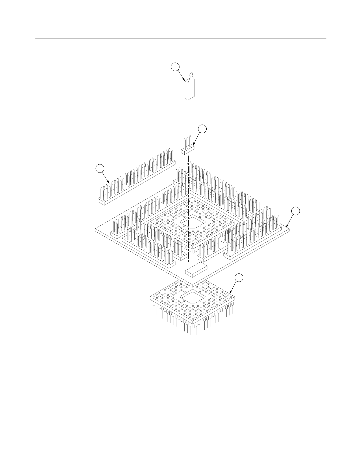
Replaceable Mechanical Parts
1
2
5
4
Figure 1: TMS320C3X probe adapter exploded view
3
TMS 702 TMS320C3X Digital Signal Processor Support Instruction Manual
6–5
Page 63

Replaceable Mechanical Parts
Replaceable mechanical parts list
Fig. &
index
number
2–3 671–2621–00 1 CIRCUIT BD ASSY: 320C31, PROBE ADAPTER 80009 671262100
–2 131–5267–00 4.5 CONN, HDR: PCB, MALE, STR, 2 X 40, 0.1 CTR, 0.235
–1 131–4356–00 2 CONN, BOX: SHUNT/SHORTING, FEMALE, 1 X 2, 0.1
Tektronix part
number
070–9831–00 1 MANUAL, TECH: INSTRUCTION, 320C3X, DISSASEMBLER,
070–9803–00 1 MANUAL, TECH:TLA 700 SERIES MICRO SUPPORT
070–9802–00 1 MANUAL, TECH: BASIC OPS MICRO SUP ON DAS/TLA 500
Serial no.
effective
Serial no.
discont’d
Qty Name & description
STANDARD ACCESSORIES
TMS 702
INSTALLATION
(SEE A02 REPL J1190, J1200, J1290, J1520, J1720, J1790)
(P1520)
OPTIONAL ACCESSORIES
SERIES LOGIC ANALYZERS
Mfr.
code
80009 070–9831–00
80009 070–9803–00
26742 9618–302–50
80009 070–9802–00
Mfr. part number
6–6
TMS 702 TMS320C3X Digital Signal Processor Support Instruction Manual
Page 64
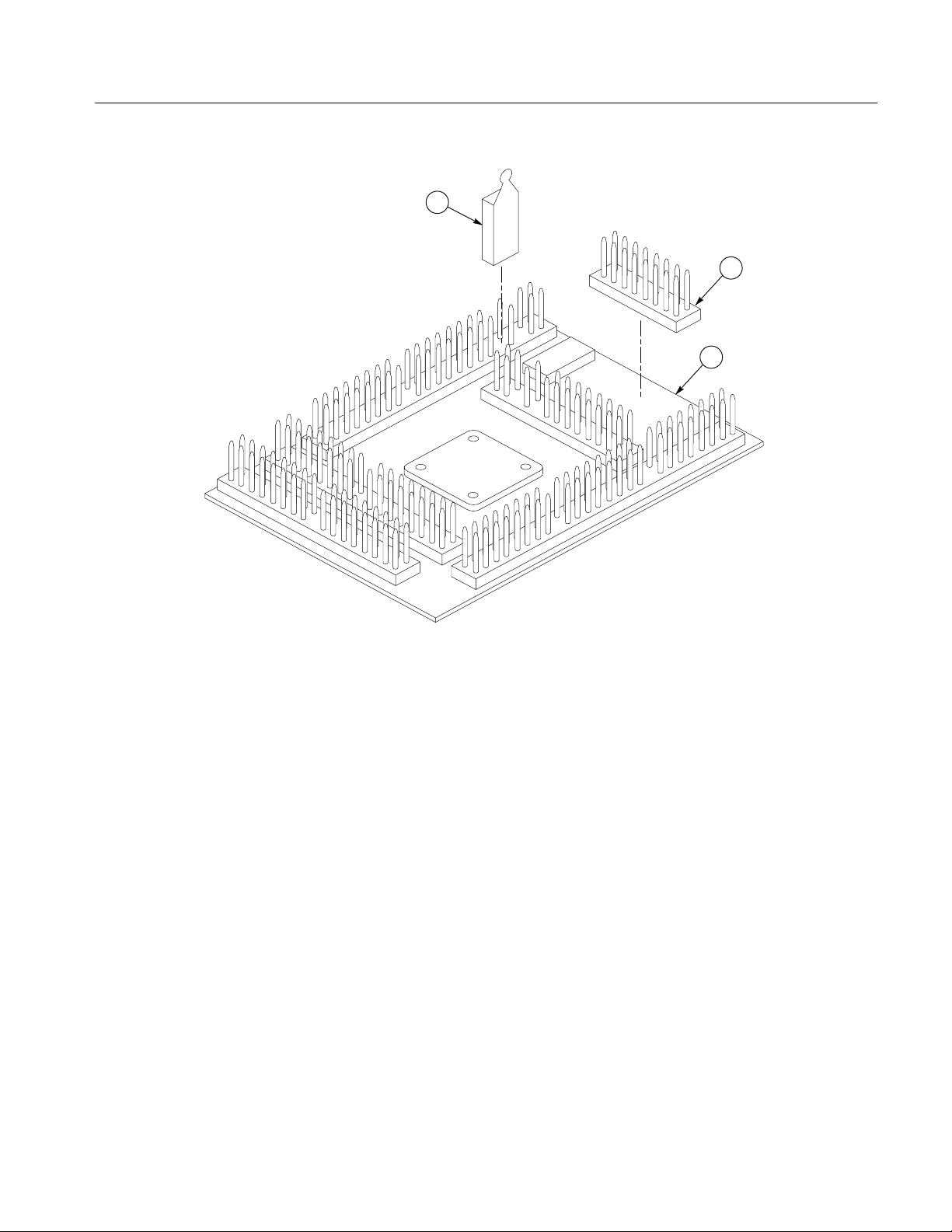
Replaceable Mechanical Parts
1
2
3
Figure 2: TMS320C3X probe adapter exploded view
TMS 702 TMS320C3X Digital Signal Processor Support Instruction Manual
6–7
Page 65

Index
A
about this manual set, ix
acquiring data, 2–5
Address group, display column, 2–7
Alternate Bus Master Cycles
clocking option, 2–2
how data is acquired, 3–14
alternate connections
extra channel probes, 3–16
to other signals, 3–15
B
basic operations, where to find information, ix
bus cycles, displayed cycle types, 2–6
bus timing, 3–14
primary and expansion bus, 3–13
C
certifications, 3–3
channel assignments
clocks, 3–12
Emulatn group, 3–12
expansion bus address group, 3–7
expansion bus Control group, 3–11
expansion bus Data group, 3–9
Intr group, 3–11
Misc group, 3–11
primary bus address group, 3–6
primary bus Control group, 3–10
primary bus Data group, 3–8
channel groups, 2–1
clock channel assignments, 3–12
clock rate, 1–2
clocking, Custom, 2–1
how data is acquired, 3–13
Clocking options
Alternate Bus Master Cycles, 3–14
Num of SW Wait, 3–15
Wait State Mode, 3–14
clocking options
Alternate Bus Master Cycles, 2–2
field names, 2–1
how data is acquired, 3–14
Num of SW Wait, 2–2
triggering on the expansion address bus, 2–4
Wait State Mode, 2–2
compliances, 3–3
connections
expansion bus signals, 1–13
no probe adapter, 1–10
channel probes, 1–11
clock probes, 1–14
other microprocessor signals, 3–15
primary bus signals, 1–11
probe adapter to SUT
PGA, 1–4
PQFP, 1–7
Contacting T ektronix, x
Control Flow display format, 2–8
Control group, symbol table, 2–3
Custom clocking, 2–1
ABM cycles, 2–2
Alternate Bus Master Cycles, 2–2
how data is acquired, primary and expansion bus,
3–13
Num od SW Wait, 2–2
Wait State Mode, 2–2
cycle types, 2–6
D
data
acquiring, 2–5
disassembly formats
Control Flow, 2–8
Hardware, 2–6
Software, 2–7
Subroutine, 2–8
how it is acquired, 3–13
data display , changing, 2–8
Data group, display column, 2–7
demonstration file, 2–9
digital signal processor, specific clocking and how data
is acquired, 3–13
dimensions, probe adapter, 3–4, 3–5
disassembled data
cycle type definitions, 2–6
viewing, 2–5
viewing an example, 2–9
disassembler
definition, ix
logic analyzer configuration, 1–2
setup, 2–1
Disassembly Format Definition overlay, 2–8
TMS 702 TMS320C3X Digital Signal Processor Support Instruction Manual
Index–1
Page 66

Index
Disassembly property page, 2–8
display formats
Control Flow, 2–8
Hardware, 2–6
Software, 2–7
special characters, 2–5
Subroutine, 2–8
E
electrical specifications, 3–2
Emulatn group, channel assignments, 3–12
environmental specifications, 3–3
expansion address bus, triggering on, 2–4
expansion bus address group, channel assignments, 3–7
expansion bus Control group, channel assignments, 3–11
expansion bus Data group, channel assignments, 3–9
H
Hardware display format, 2–6
cycle type definitions, 2–6
I
installing hardware. See connections
Intr group, channel assignments, 3–11
Misc group, channel assignments, 3–11
Mnemonics display column, 2–7
N
Num of SW Wait
clocking option, 2–2
how data is acquired, 3–15
P
primary bus address group, channel assignments, 3–6
primary bus Control group, channel assignments, 3–10
primary bus Data group, channel assignments, 3–8
probe adapter
circuit description, 4–1
clearance, 1–3
adding sockets, 1–6
dimensions, 3–4, 3–5
configuring, 1–3, 3–1
connecting leads, 1–8
hardware description, 3–1
jumper positions, 3–1
disassembly and timing, 1–3
not using one, 1–10
placing the microprocessor in, 1–6
Processor, definition, ix
J
jumpers, Disassembly/Timing, 1–3, 3–1
L
leads (podlets). See connections
logic analyzer
configuration for disassembler, 1–2
software compatibility, 1–2
M
manual
conventions, ix
how to use the set, ix
Mark Cycle function, 2–9
Mark Opcode function, 2–9
marking cycles, definition of, 2–9
microprocessor
package types supported, 1–1
signals not accessible on probe adpter, 3–15
R
reference books, 1–1
reference memory, 2–9
restrictions, 1–2
without a probe adapter, 1–10
S
Sample column, 2–7
service information, 4–1
setups, disassembler, 2–1
signals
active low sign, x
extra channel probes, 3–16
Software display format, 2–7
special characters displayed, 2–5
specifications, 3–1
certifications, 3–3
channel assignments, primary and expansion bus, 3–6
compliances, 3–3
electrical, 3–2
environmental, 3–3
Index–2
TMS 702 TMS320C3X Digital Signal Processor Support Instruction Manual
Page 67

Index
mechanical (dimensions), 3–4, 3–5
Subroutine display format, 2–8
support setup, 2–1
SUT, definition, ix
symbol table, Control channel group, 2–3
system file, demonstration, 2–9
T
terminology, ix
Timestamp display column, 2–7
triggering, triggering on the expansion address bus, 2–4
V
viewing disassembled data, 2–5
W
Wait State Mode
clocking option, 2–2
how data is acquired, 3–14
TMS 702 TMS320C3X Digital Signal Processor Support Instruction Manual
Index–3
 Loading...