

Page 1

Instruction Manual
TMS568
MPC85XX Microprocessor Software Support
071-1191-00
www.tektronix.com
Page 2

Copyright © Tektronix, Inc. All rights reserved.
Tektronix products are covered by U.S. and foreign patents, issued and pending. Information in this public ation supercedes
that in all previously published material. Specifications and price c hange privileges reserved.
Tektronix, Inc., P.O. Box 500, Beaverton, OR 97077
TEKTRONIX and TEK are registered trademarks of Tektronix, Inc.
MagniVu is a trademark of Tektronix, Inc.
Page 3

SOFTWARE WARRANTY
Tektronix warrants that the media on which this software product is furnished and the encoding of the programs on
the media will be free from defects in materials and workmanship for a period of three (3) months from the date of
shipment. If a medium or encoding proves defective during the warranty period, Tektronix will provide a
replacement in exchange for the defective medium. Except as to the media on which this software product is
furnished, this software product is provided “as is” without warranty of any kind, either express or implied.
Tektronix does not warrant that the functions contained in this software product will meet Customer’s
requirements or that the operation of the programs will be uninterrupted or error-free.
In order to obtain service under this warranty, Customer must notify Tektronix of the defect before the expiration
of the warranty period. If Tektronix is unable to provide a replacement that is free from defects in materials and
workmanship within a reasonable time thereafter, Customer may terminate the license for this software product
and return this software product and any associated materials for credit or refund.
THIS WARRANTY IS GIVEN BY TEKTRONIX IN LIEU OF ANY OTHER WARRANTIES, EXPRESS
OR IMPLIED. TEKTRONIX AND ITS VENDORS DISCLAIM ANY IMPLIED WARRANTIES OF
MERCHANTABILITY OR FITNESS FOR A PARTICULAR PURPOSE. TEKTRONIX’
RESPONSIBILITY TO REPLACE DEFECTIVE MEDIA OR REFUND CUSTOMER’S PAYMENT IS
THE SOLE AND EXCLUSIVE REMEDY PROVIDED TO THE CUSTOMER FOR BREACH OF THIS
WARRANTY. TEKTRONIX AND ITS VENDORS WILL NOT BE LIABLE FOR ANY INDIRECT,
SPECIAL, INCIDENTAL, OR CONSEQUENTIAL DAMAGES IRRESPECTIVE OF WHETHER
TEKTRONIX OR THE VENDOR HAS ADVANCE NOTICE OF THE POSSIBILITY OF SUCH
DAMAGES.
Page 4

Page 5

Table of Contents
Getting Started
Operating Basics
Preface xi...................................................
Manual Conventions xi..............................................
Contacting Tektronix xii.............................................
Support Package Descri ption 1--1.......................................
Disassembly Support 1--1..........................................
Logic Analyzer Software Compatibility 1--2..............................
Logic Analyzer Configuration 1--2......................................
Module Requirements 1--2.........................................
Probe Requirements 1--2..........................................
Requirements and Restrictions 1--3......................................
Hardware Reset 1--3..............................................
Clock Rate 1--3..................................................
Setup/Hold Time Adjustments 1--3..................................
Nonintrusive Acquisition 1--4......................................
Limitations of the Support 1--4.........................................
Connecting the Logic Analyzer to a Target System 1--4.....................
Labeling P6434 and P6860 Probes 1--5...................................
Setting Up the Support 2--1.....................................
Installing the Support Software 2--1.....................................
Support Package Setups 2--2...........................................
Clocking Options 2--2................................................
85XXDDR and 85XXDDR_RW Support Packages 2--2..................
85XXLB, 85XXLB_ALT, and 85XXLB_ADS Support Packages 2--3.......
Acquiring and Viewing Disassembled Data 2--5....................
Acquiring Data 2--5..................................................
Changing How Data is Displayed 2--5...................................
Optional Display Selections 2--6....................................
Microprocessor Specific Fields for the 85XXDDR Support Package 2--6....
Microprocessor Specific Fields for the 85XXDDR_RW Support Package 2--9
Microprocessor Spec ific Fields for the 85XXLB, 85XXLB_ALT, and
85XXLB_ADS Support Package 2--10.........................
Cycle Type Labels 2--11...............................................
Interrupt and Exception Labels 2--12.....................................
Special Characters 2--13...............................................
Viewing Disassembled Data 2--14........................................
Hardware Display Format 2--15......................................
Software Display Format 2--17.......................................
Control Flow Display Format 2--20...................................
Subroutine Display Format 2--21.....................................
Marking Cycles 2--21..............................................
Viewing an Example of Disassembled Data 2--22...........................
TMS568 MPC85XX Microprocessor Software Support
i
Page 6

Table of Contents
Reference
Channel Group Definitions 3--1..................................
Channel Groups 3--1.................................................
Symbol and Channel Assignment Tables 3--5......................
Symbol Tables 3--5..................................................
Channel Assignment Tables 3--8........................................
85XXDDR Channel Group Assignments 3--9..........................
85XXDDR_RW Channel Group Assignments 3--21......................
85XXLB Support Package Group Assignments 3--39.....................
85XXLB_ALT Support Package Group Assignments 3--43................
85XXLB_ADS Support Package Group Assignments 3--48................
Clock and Qualifier Channel Assignments 3--52.........................
Signals Required for Clocking and Disassembly 3--54....................
Signals Not Required for Clocking and Disassembly 3--54.................
Signal Source To Probe Connections 3--55.................................
Connections for the 85XXDDR Support Package 3--60...................
Connections for the 85XXDDR_RW Support Package 3--67...............
Connections for the 85XXLB Support Package 3--74.....................
Connections for 85XXLB_ALT Support Package 3--79...................
Connections for 85XXLB_ADS Support Package 3--89...................
Signal Acquisition 3--95.........................................
Specification
Replaceable Parts List
Index
Specifications Table 4--1..............................................
Parts Ordering Information 5 --1.........................................
Using the Replaceable Parts List 5--1....................................
ii
TMS568 MPC85XX Microprocessor Software Support
Page 7

List of Figures
Table of Contents
Figure 2--1: Address Multiplexing for DDR--SDRAM memories. 2--8...
Figure 2--2: 85XXDDR hardware display format 2--15................
Figure 2--3: 85XXDDR_RW hardware display format 2--16...........
Figure 2--4: 85XXLB_ALT hardware display format 2--17............
Figure 2--5: 85XXDDR software display format 2--18.................
Figure 2--6: 85XXDDR_RW software display format 2--19............
Figure 2--7: 85XXLB_ALT software display format 2--20.............
Figure 3--1: P6860 probe land footprint for MA--A0/A1 and
M A -- A 2 / A 3 3 -- 5 6............................................
Figure 3--2: P6860 probe land footprint for MA--E2/E3 and
S L -- A 0 / A 1 3 -- 5 6.............................................
Figure 3--3: P6860 probe land footprint for SL--A0/A1 and
S L -- A 2 / A 3 3 -- 5 7.............................................
Figure 3--4: P6860 probe land footprint for SL--C2/C3 and
S L -- E 2 / E 3 3 -- 5 7.............................................
Figure 3--5: P6860 Probe land footprint for E LB--A2/A3 and
E L B -- A 0 / A 1 3 -- 5 9...........................................
Figure 3--6: P6860 Probe land footprint for E LB--D2/D3 and
E L B -- D 0 / D 1 3 -- 5 9...........................................
Figure 3--7: P6860 Probe land footprint for E LB--C2/C3 and
E L B -- C 0 / C 1 3 -- 6 0...........................................
Figure 3--8: Timing diagram for Local bus interface 3--95.............
Figure 3--9: Timing diagram for DDR SDRAM interface 3--98.........
TMS568 MPC85XX Microprocessor Software Support
iii
Page 8

Table of Contents
List of Tables
Table 1--1: Module requirements 1--2.............................
Table 1--2: Probe requirements 1--2..............................
Table 1--3: Setup/Hold time requirements for the MPC85XX
product 1--3..............................................
Table 2--1: Logic analyzer disassembly display options 2--6..........
Table2--2:Cycletypelabels 2--11.................................
T able 2--3: Computed cycle type labels 2--12........................
T able 2--4: Special messages and their descriptions 2--13.............
Table 2--5: Mark selections and definitions in 85XXLB,
85XXLB_ALT, and 85XXLB_ADS 2--21.......................
Table 2--6: Mark selections and definitions in 85XXDDR and
85XXDDR_RW 2--22........................................
Table 3--1: 85XXDDR support package channel groups 3--1.........
Table 3--2: 85XXDDR_RW support package channel groups 3--2.....
Table 3--3: 85XXLB, 85XXLB_ALT, 85XXLB_ADS support
package channel groups 3--3................................
Table 3--4: 85XXLB, 85XXLB_ALT, 85XXLB_ADS ChipSel
group symbol table definitions 3--5..........................
Table 3--5: 85XXLB, 85XXLB_ALT, 85XXLB_ADS Control group
symbol table definitions 3--6................................
Table 3--6: 85XXLB, 85XXLB_ALT, 85XXLB_ADS, 85XXDDR,
and 85XXDDR_RW Debug group symbol table definitions 3--7...
Table 3--7: 85XXDDR AND 85XXDDR_RW Control group symbol
table definitions 3--8.......................................
Table 3--8: Address group assign ments for 85XXDDR support
package 3--9..............................................
Table 3--9: BankAddr group assignments for 85XXDDR support
package 3--9..............................................
Table 3--10: DataLo group assignments for 85XXDDR support
package 3--10..............................................
Table 3--11: DataHi group assignments for 85XXDDR support
package 3--11..............................................
Table 3--12: Control group assignments for 85XXDDR support
package 3--12..............................................
Table 3--13: Command group assignments for 85XXDDR support
packages 3--13.............................................
iv
TMS568 MPC85XX Microprocessor Software Support
Page 9

Table of Contents
Table 3--14: Strobes group assignments for 85XXDDR support
package 3--13..............................................
Table 3--15: ChipSel group assignments for 85XXDDR support
package 3--14..............................................
Table 3--16: CheckBits group assignments for 85XXDDR support
package 3--14..............................................
Table 3--17: WrtMasks group assignments for 85XXDDR support
package 3--14..............................................
Table 3--18: Debug group assignments for the 85XXDDR support
package 3--15..............................................
Table 3--19: Misc group assignments for 85XXDDR support
package 3--15..............................................
Table 3--20: UserDefined group assignments for the 85XXDDR
support package 3--16.......................................
Table 3--21: DatByte0 group assignments for 85XXDDR support
package 3--16..............................................
Table 3--22: DatByte1 group assignments for 85XXDDR support
package 3--17..............................................
Table 3--23: DatByte2 group assignments for 85XXDDR support
package 3--17..............................................
Table 3--24: DatByte3 group assignments for 85XXDDR support
package 3--18..............................................
Table 3--25: DatByte4 group assignments for 85XXDDR support
package 3--18..............................................
Table 3--26: DatByte5 group assignments for 85XXDDR support
package 3--19..............................................
Table 3--27: DatByte6 group assignments for 85XXDDR support
package 3--19..............................................
Table 3--28: DatByte7 group assignments for 85XXDDR support
package 3--20..............................................
Table 3--29: Address group assignments for 85XXDDR_RW
support package 3--21.......................................
Table 3--30: BankAddr group assignments for 85XXDDR_RW
support package 3--21.......................................
Table 3--31: RdDatLo group assignments for 85XXDDR_RW
support package 3--22.......................................
Table 3--32: RdDatHi group assignments for 85XXDDR_RW
support package 3--23......................................
Table 3--33: WrDatLo group assignments for 85XXDDR_RW
support package 3--24.......................................
Table 3--34: WrDatHi group assignments for 85XXDDR_RW
support package 3--26.......................................
TMS568 MPC85XX Microprocessor Software Support
v
Page 10

Table of Contents
Table 3--35: Control group assignments for 85XXDDR_RW
support package 3--27.......................................
Table 3--36: Command group assignments for 85XXDDR_RW
support package 3--27.......................................
Table 3--37: Strobes group assignments for 85XXDDR_RW
support package 3--28......................................
Table 3--38: ChipSel assignments for 85XXDDR_RW support
package 3--28..............................................
Table 3--39: CheckBits group assignments for 85XXDDR_RW
support package 3--29.......................................
Table 3--40: WrtMasks group assignments for 85XXDDR_RW
support package 3--29.......................................
Table 3--41: Debug group assignments for 85XXDDR_RW
support package 3--30.......................................
Table 3--42: Misc group assignments for 85XXDDR_RW support
package 3--30..............................................
Table 3--43: UserDefined group assignments for 85XXDDR_RW
support package 3--30.......................................
Table 3--44: RDDatBy0 group assignments for 85XXDDR_RW
support package 3--31.......................................
Table 3--45: RDDatBy1 group assignments for 85XXDDR_RW
support package 3--32.......................................
Table 3--46: RDDatBy2 group assignments for 85XXDDR_RW
support package 3--32.......................................
Table 3--47: RDDatBy3 group assignments for 85XXDDR_RW
support package 3--33.......................................
Table 3--48: RDDatBy4 group assignments for 85XXDDR_RW
support package 3--33.......................................
Table 3--49: RDDatBy5 group assignments for 85XXDDR_RW
support package 3--34......................................
Table 3--50: RDDatBy6 group assignments for 85XXDDR_RW
support package 3--34......................................
Table 3--51: RDDatBy7 group assignments for 85XXDDR_RW
support package 3--35.......................................
Table 3--52: WRDatBy0 group assignments for 85XXDDR_RW
support package 3--35.......................................
Table 3--53: WRDatBy1 group assignments for 85XXDDR_RW
support package 3--36.......................................
Table 3--54: WRDatBy2 group assignments for 85XXDDR_RW
support package 3--36......................................
Table 3--55: WRDatBy3 group assignments for 85XXDDR_RW
support package 3--37.......................................
vi
TMS568 MPC85XX Microprocessor Software Support
Page 11

Table of Contents
Table 3--56: WRDatBy4 group assignments for 85XXDDR_RW
support package 3--37.......................................
Table 3--57: WRDatBy5 group assignments for 85XXDDR_RW
support package 3--38.......................................
Table 3--58: WRDatBy6 group assignments for 85XXDDR_RW
support package 3--38.......................................
Table 3--59: WRDatBy7 group assignments for 85XXDDR_RW
support package 3--39.......................................
Table 3--60: Address and Data group assignments for 85XXLB
support package 3--39.......................................
Table 3--61: BurstAddr group assignments for 85XXLB support
package 3--41..............................................
Table 3--62: Control group assignments for 85XXLB support
package 3--41..............................................
Table 3--63: ChipSel group assignments for 85XXLB support
package 3--42..............................................
Table 3--64: Debug group assignments for 85XXLB support
packages 3--42.............................................
Table 3--65: DataMask group assignments for 85XXLB support
package 3--43..............................................
Table 3--66: UserDefined group assignments for 85XXLB support
package 3--43..............................................
Table 3--67: Address group assignments for 85XXLB_ALT support
package 3--43..............................................
Table 3--68: Data group assignments for 85XXLB_ALT support
package 3--45..............................................
Table 3--69: BurstAddr group assignments for 85XXLB_ALT
support package 3--46.......................................
Table 3--70: Control group assignments for 85XXLB_ALT support
package 3--46..............................................
Table 3--71: ChipSel group assignments for 85XXLB_ALT support
package 3--47..............................................
Table 3--72: Debug group assignments for 85XXLB_ALT support
package 3--47..............................................
Table 3--73: DataMask group assignments for 85XXLB_ALT
support package 3--48.......................................
Table 3--74: UserDefined group assignments for 85XXLB_ALT
support package 3--48.......................................
Table 3--75: Address and Data group assignments for 85XXLB_ADS
support package 3--48.......................................
Table 3--76: BurstAddr group assignments for 85XXLB_ADS
support package 3--50.......................................
TMS568 MPC85XX Microprocessor Software Support
vii
Page 12

Table of Contents
Table 3--77: Control group assignments for 85XXLB_ADS support
package 3--50..............................................
Table 3--78: ChipSel group assignments for 85XXLB_ADS support
package 3--51..............................................
Table 3--79: Debug group assignments for 85XXLB_ADS support
package 3--51..............................................
Table 3--80: DataMask group assignments for 85XXLB_ADS
support package 3--51.......................................
Table 3--81: UserDefined group assignments for 85XXLB_ADS
support package 3--52.......................................
Table 3--82: Clock and Qualifier channel assignments for 85XXDDR
support package 3--52.......................................
Table 3--83: Clock and Qualifier channel assignments for
85XXDDR_RW support package 3--52.........................
Table 3--84: Clock and Qualifier channel assignments for 85XXLB
suppor t package 3--53......................................
Table 3--85: Clock and Qualifier channel assignments for
85XXLB_ALT support package 3--53..........................
Table 3--86: Clock and Qualifier channel assignments for
85XXLB_ADS support package 3--54..........................
Table 3--87: Recommended pin assignments for a P6434 Mictor
connector (component side) 3--55..............................
Table 3--88: Footprint to logic analyzer mapping for the 85XXDDR
support package 3--58.......................................
Table 3--89: Footprint to logic analyzer mapping for the
85XXDDR_RW support package 3--58.........................
Table 3--90: MA--A2/A3 probe connections for 85XXDDR support
package 3--60..............................................
Table 3--91: MA--A0/A1 probe connections for 85XXDDR support
package 3--61..............................................
Table 3--92: MA--C2/C3 probe connections for the 85XXDDR
support package 3--62.......................................
Table 3--93: MA--E2/E3 probe connections for 85XXDDR support
package 3--62..............................................
Table 3--94: SL--A2/A3 probe connections for 85XXDDR support
package 3--63..............................................
Table 3--95: SL--A0/A1 probe connections for 85XXDDR support
package 3--64..............................................
Table 3--96: SL--C2/C3 probe connections for 85XXDDR support
package 3--65..............................................
Table 3--97: SL--E2/E3 probe connections for 85XXDDR support
package 3--65..............................................
viii
TMS568 MPC85XX Microprocessor Software Support
Page 13

Table of Contents
Table 3--98: MA--A2/A3 probe connections for 85XXDDR_RW
support package 3--67......................................
Table 3--99: MA--A0/A1 probe connections for 85XXDDR_RW
support package 3--67.......................................
Table 3--100: MA--C2/C3 probe connections for 85XXDDR_RW
support package 3--68......................................
Table 3--101: MA--E2/E3 probe connections for 85XXDDR_RW
support package 3--69.......................................
Table 3--102: SL--A2/A3 probe connections for 85XXDDR_RW
support package 3--70.......................................
Table 3--103: SL--A0/A1 probe connections for 85XXDDR_RW
support package 3--71.......................................
Table 3--104: SL--C2/C3 probe connections for 85XXDDR_RW
support package 3--71.......................................
Table 3--105: SL--E2/E3 probe connections for 85XXDDR_RW
support package 3--72.......................................
Table 3--106: Mictor A connections for 85XXLB support
package 3--74..............................................
Table 3--107: Mictor C connections for 85XXLB support package
(Probe #3) 3--75............................................
Table 3--108: Mictor D connections for 85XXLB support package
(Probe #3) 3--76............................................
Table 3--109: A3/A2 connections using P6860 probe for 85XXLB
support package 3--76......................................
Table 3--110: C3/C2 connections using P6860 probe for 85XXLB
support package 3--77.......................................
Table 3--111: A1/A0 connections using P6860 probe for 85XXLB
support package 3--78......................................
Table 3--112: Address connections for 85XXLB_ALT support
package 3--79..............................................
Table 3--113: Data connections for 85XXLB_ALT support
package 3--81..............................................
Table 3--114: Control connections for 85XXLB support
package 3--82..............................................
Table 3--115: ELB--A2/A3 probe head assignment for
85XXLB_ALT support package 3--84..........................
Table 3--116: ELB--A0/A1 probe head assignment for
85XXLB_ALT support package 3--85..........................
Table 3--117: ELB--D2/D3 probe head assignment for
85XXLB_ALT support package 3--85..........................
Table 3--118: ELB--A0/A1 probe head assignment for
85XXLB_ALT support package 3--86..........................
TMS568 MPC85XX Microprocessor Software Support
ix
Page 14

Table of Contents
Table 3--119: ELB--C2/C3 probe head assignment for
85XXLB_ALT support package 3--87..........................
Table 3--120: ELB--D0/D1 probe head assignment for
85XXLB_ALT support package 3--88..........................
Table 3--121: Alternate Board Data connections 3--89................
Table 3--122: Alternate Board Control connections 3-- 90..............
Table 3--123: A3/A2 probe head assignment for 85XXLB_ADS
support package 3--91.......................................
Table 3--124: A1/A0 probe head assignment for 85XXLB_ADS
support package 3--92.......................................
Table 3--125: C3/C2 probe head assignment for 85XXLB_ADS
support package 3--93......................................
Table 3--126: D1/D0 probe head assignment for 85XXLB_ADS
support package 3--94.......................................
Table 3--127: Sample points for 85XXLB, and 85XXLB_ADS
support packages 3--96......................................
Table 3--128: Sample points for 85XXLB_ALT support
package 3--96..............................................
Table 3--129: Signal accquisition for 85XXLB, 85XXLB_ALT,
and 85XXLB_ADS support packages 3--97.....................
Table 3--130: Sample points for 85XXDDR and 85XXDDR_RW
support packages 3--98......................................
Table 3--131: Signal acquisition in 85XXDDR and 85XXDDR_RW
support packages 3--99......................................
T able 4--1: Electrical specifications 4--1..........................
x
TMS568 MPC85XX Microprocessor Software Support
Page 15

Preface
This instruction manual contains specific information about the TMS568
MPC85XX microprocessor support product and is part of a set of information on
how to operate this product on compatible Tektronix logic analyzers.
If you are familiar with operating microprocessor support packages on the logic
analyzer for which the TMS568 MPC85XX microprocessor support product was
purchased, you will probably only need this instruction manual to set up and run
the support.
If you are not familiar with operating microprocessor support packages, you will
need to supplement this instruction manual with information on basic operations
to set up and run the support.
Information on basic operations of microprocessor s upport packages is included
with each product. Each logic analyzer includes basic information that describes
how to perform tasks common to s upport packages on that platform. This
information can be in the form of logic analyzer online help, an installation
manual, or a user manual.
This manual provides detailed information on the following topics:
Manual Conventions
H Connecting the logic analyzer to the target system
H Setting up the logic analyzer to acquire data from the target system
H Acquiring and viewing disassembled data
This manual uses the following conventions:
H The term “disassembler” refers to the software that disassembles
microprocessor cycles into instruction mnemonics and cycle types.
H The phrase “basic operations” refers to the logic analyzer online help, or the
user manual that covers the basic operations of the microprocessor support.
H The phrase “logic analyzer” refers to the Tektronix logic analyzer for which
this product was purchased.
TMS568 MPC85XX Microprocessor Software Support
xi
Page 16

Preface
Contacting Tektronix
Phone 1-800-833-9200*
Address Tektronix, Inc.
Department or name (if known)
14200 SW Karl Braun Drive
P.O. Box 500
Beaverton, OR 97077
USA
Web site www.tektronix.com
Sales support 1-800-833-9200, select option 1*
Service support 1-800-833-9200, select option 2*
Technical support Email: techsupport@tektronix.com
1-800-833-9200, select option 3*
6:00 a.m. -- 5:00 p.m. Pacific time
* This phone number is toll free in North America. After office hours, please leave a
voice mail message.
Outside North America, contact a Tektronix sales office or distributor; see the
Tektronix web site for a list of offices.
TMS568 MPC85XX Microprocessor Software Support
xii
Page 17

Getting Started
Page 18

Page 19

Getting Started
This section contains information on the TMS568 MPC85XX microprocessor
support product and information on connecting your logic analyzer to your target
system.
Support Package Description
The TMS568 MPC85XX microprocessor support product displays disassembled
data from systems based on MPC8540/8560. The support package allows you to
acquire microprocessor cycles with minimal impact on the environment of the
system.
The TMS568 MPC85XX microprocessor support product contains five support
packages that have their own setup software and disassemblers. A description of
each support package is listed here:
H 85XXDDR acquires DDR commands and DDR reads or DDR writes.
H 85XXDDR_RW acquires commands and both DDR reads and writes
simultaneously.
Disassembly Support
H 85XXLB acquires the SDRAM and GPCM cycles on the local bus.
H 85XXLB_ALT acquires the SDRAM and GPCM bus cycles from 85XX
local bus interface. This support package can be used with reference boards
having alternate channel assignment. Refer to the channel assignment section
for details.
H 85XXLB_ADS acquires the SDRAM and GPCM bus cycles from 85XX
local bus interface. This support package is compatible with Motorola ADS
reference board channel assignment.
The disassembler decodes information from the DDR and local bus interfaces.
To use this support package efficiently refer to the following documents:
H MPC8540 INTEGRATED PROCESSOR PRELIMINARY USER’S MANUAL,
{Motorola, MPC8540xxxx 3/2002, Rev.1.3}
H MPC8560 PowerQUICC III INTEGRATED COMMUNICATION PROC-
ESSOR PRELIMINARY USER’S MANUAL, {Motorola MPC8560xxxx,
1/2003, Rev.2.0}
H JEDEC STANDARD, DDR SDRAM Specification, JESD79, Release 2, May
2002.
TMS568 MPC85XX Microprocessor Software Support
1--1
Page 20

Getting Started
H NEX_SPA (Sample point analyzer), Nexus technologies( www.bus-
boards.com).
Logic Analyzer Software Compatibility
The label on the microprocessor support CD-ROM states which version of logic
analyzer software this support package is compatible with.
Logic Analyzer Configuration
The TMS568 product allows a choice of required minimum module configurations.
Module Requirements
Probe Requirements
Table 1--1 lists the minimum module requirements for the TMS568 MPC85XX
microprocessor support product.
Table 1--1: Module requirements
Support package Module requirements
85XXDDR One TLA7Ax4 450 MHz, 136-channel module
85XXDDR_RW Two TLA7Ax4 450 MHz, 136-channel modules in merged
configuration
85XXLB One TLA7N2 module 200 MHz, 68-channel module
85XXLB_ALT One TLA7N3 module 200 MHz, 102-channel module
85XXLB_ADS TLA7Ax2 module 235 MHz state speed, 68-channel
module
Table 1--2 lists the probe requirements for the TMS568 MPC85XX
microprocessor support product.
Table 1--2: Probe requirements
Support package Probe requirements
85XXDDR Four P6860 probes
1--2
85XXDDR_RW Eight P6860 probes
85XXLB Two P6434 probes
85XXLB_ALT Three P6434 probes
85XXLB_ADS Two P6860 probes
TMS568 MPC85XX Microprocessor Software Support
Page 21

Getting Started
Requirements and Restrictions
Review the electrical specifications in the Specifications section on page 4--1 in
this manual as they pertain to your target system, as well as the following
descriptions of TMS568 MPC85XX microprocessor support product require ments and restrictions.
Hardware Reset
Clock Rate
Setup/Hold Time
Adjustments
If a hardware reset occurs in your target system during an acquisition, the
application disassembler might acquire an invalid sample.
The maximum clock rate for local bus is 166 MHz and for DDR--SDRAM is 200
MHz.
The DDR reads and writes have different timings. The DQS and data are edge
aligned for reads and center aligned for writes. 85XXDDR support package has
default setup hold timings valid for reads. To capture write data accurately or if
the DDR SDRAM timings are different, you need to adjust the setup/hold timing
values. This can be done either manually or using a tool.
To manually adjust setup/hold, trigger on a read or a write cycle appropriately.
Then, in the MagniVu, find the data valid window for DDR data with reference
to the clock edge. Select setup/hold timings in custom clocking option, in such a
way that the setup/hold window falls at the center of the data valid window.
To assist in this operation, a software tool called DDR Sample Point Analysis
Software (NEX-SPA) is available from Nexus Technology, Inc (a Tektronix
Embedded System Tools Partner). The tool and a user guide can be downloaded
from their web site, www.busboards.com.
Table 1--3 lists the setup/hold time requirements for the different support
packages. For correct acquisition, the target system must provide a data valid
window meeting these requirements.
Table 1--3: Setup/Hold time requirements for the MPC85XX product
Support package
name
85XXDDR One TLA7Ax4 450 MHz,
85XXDDR_RW Two TLAAx4 450 MHz,
85XXLB One TLA7N2 module 200
Logic analyzer/ module Setup time Hold time
136--channel module
136--channel modules in
merged configuration
MHz, 68--channel module
TMS568 MPC85XX Microprocessor Software Support
750 ps 0ps
750 ps 0ps
2.5 ns 0ps
1--3
Page 22

Getting Started
Table 1--3: Setup/Hold time requirements for the MPC85XX product (Cont.)
Support package
name
85XXLB_ALT One TLA7N3 module 200
MHz, 102--channel module
2.5 ns 0ps
Hold timeSetup timeLogic analyzer/ module
85XXLB_ADS TLA7Ax2 module 235 MHz
state speed, 68--channel
module
Nonintrusive Acquisition
Acquiring microprocessor cycles is nonintrusive to the target system. The
TMS568 MPC85XX microprocessor support product does not intercept, modify,
or present signals back to the system under test.
Limitations of the Support
The TMS568 MPC85XX microprocessor support product does not support the
following:
H Local Bus SDRAM extended CAS Latency “4,5,6,7”.
H UPM cycles.
Connecting the Logic Analyzer to a Target System
You can use the channel probes to make the connections between the logic
analyzer and your target system.
2.5 ns 0ps
1--4
To connect the probes to the target system as described in the TMS568
MPC85XX microprocessor support product channel assignment, follow the
steps:
1. Power off your target system. It is not necessary to power off the logic
analyzer.
CAUTION. To prevent static damage, handle the target systems, probes, and the
logic analyzer module in a static-free environment. Static discharge can damage
these components.
Always wear a grounding wrist strap, heel strap, or similar device while
handling the target system.
2. Place the target system on a horizontal, static-free surface.
TMS568 MPC85XX Microprocessor Software Support
Page 23

Getting Started
3. Use tables 3--87 through 3--126 starting on page 3--55 to connect the channel
probes to the necessary signals in the target system.
A probe adapter (NEX--DDRHS) that connects the Logic Analyzer to a JEDEC
standard DDR--SDRAM slot is available from Nexus Technology Inc. (a
Tektronix Embedded Systems Tools Partner). TMS568 DDR--SDRAM supports
are compatible with this probe adapter. When using this probe adapter, an
automatic dequeue feature is available only if the Debug signals are routed
through the ECC pins.
Contact your Tektronix representative if you require any assistance regarding the
probe adapter.
Labeling P6434 and P6860 Probes
The TMS568 MPC85XX microprocessor support product relies on the channel
mapping and labeling scheme for the P6860 and P6434 Probes. Apply labels,
using the instructions described in the P6810, P6860, and P6880 Logic Analyzer
Probes Instruction manual and P6434 Logic Analyzer Probes Instruction manual.
TMS568 MPC85XX Microprocessor Software Support
1--5
Page 24

Getting Started
1--6
TMS568 MPC85XX Microprocessor Software Support
Page 25

Operating Basics
Page 26

Page 27

Setting Up the Support
This section provides information on how to set up the software support and
covers the following topics:
H Installing the support software
H Support package setups
H Clocking options
The information in this section pertains to the specific operations and functions
of the TMS568 MPC85XX microprocessor support product on a Tektronix logic
analyzer.
Before you acquire and display disassembled data, you need to load the support
package and specify the setups for clocking and triggering as described in the
logic analyzer online help under “Microprocessor support”. The support package
provides default values for each of these setups, but you can change the setups as
needed.
Installing the Support Software
NOTE. Before you install any software, it is recommended you verify that the
microprocessor support software is compatible with the logic analyzer software.
To install the TMS568 MPC85XX microprocessor support product on your
Tektronix logic analyzer, follow these steps:
1. Insert the CD-ROM in the CD drive.
2. Click the Windows Start button, point to Settings, and click Control Panel.
3. In the Control Panel window, double-click Add/Remove Programs.
4. Follow the instructions on the screen for installing the software from the
CD-ROM. A copy of the instruction manual is available on the CD-ROM.
To remove or uninstall software, follow the above instructions and select
Uninstall. You need to close all windows before you uninstall any software.
The TMS568 MPC85XX microprocessor support product installs five different
support packages.
TMS568 MPC85XX Microprocessor Software Support
2--1
Page 28

Setting Up the Support
Support Package Setups
The TMS568 MPC85XX microprocessor support product installs five support
packages that have their own setup s oftware and disassemblers. A description of
each support package is listed here:
H 85XXDDR: This support package acquires DDR commands and DDR reads
H 85XXDDR_RW: This support package acquires commands and both DDR
H 85XXLB: This support package acquires the SDRAM and GPCM cycles on
H 85XXLB_ALT: This support package acquires SDRAM and GPCM bus
or DDR writes.
reads and writes simultaneously.
the local bus.
cycles from 85XX local bus interface. Use this package with reference
boards that have alternate channel assignment. Refer to the channel
assignment section for more details.
Clocking Options
85XXDDR and
85XXDDR_RW Support
Packages
H 85XXLB_ADS: This support package is compatible with Motorola ADS
reference board channel assignment. This support package acquires SDRAM
and GPCM bus cycles from 85XX local bus interface.
The TMS568 MPC85XX microprocessor support product adds these five
selections to the “Load Support Package” dialog box, under the File pulldown
menu.
A special custom clocking program is loaded into the module every time you
load one of the 85XXDDR, 85XXDDR_RW, 85XXLB, 85XXLB_ALT or
85XXLB_ADS support packages from the TMS568 MPC85XX microprocessor
support product. Each support package offers different clocking options. You
may use the default clocking option or choose an alternate by clicking the
“More...” button in the logic analyzer setup window.
The software provides three custom clocking options for the 85XXDDR and
85XXDDR_RW support packages.
DDR Clocking. Permits selection between DDR clocks (MCK0, MCK1, MCK2)
and chip selects (MCS0 or/and MCS1) to acquire DDR data. Select the
approriate option from the following:
2--2
DDR MCK0; MCS0~ only active (default)
DDR MCK0; MCS0~ and MCS1~active
DDR MCK1; MCS0~ only active
TMS568 MPC85XX Microprocessor Software Support
Page 29

Setting Up the Support
DDR MCK1; MCS0~ and MCS1~active
DDR MCK2; MCS0~ only active, or
DDR MCK2; MCS0~ and MCS1~active
Clock Mode. Select the type of data acquisition.
Selective Clocking (default)
This mode reduces the number of idle cycles stored by the acquisition card to
optimally use the acquisition memory. Data is stored whenever MRAS~ or
MCAS~ is asserted, along with CS0~ or CS1~. After every assertion of MCAS~,
additional 17 samples are taken on every DDR Clock edge. If MCAS~ and
ChipSelect are asserted during these 17 samples, the count is reset.
NOTE. This mode does not work if the DDR target uses ChipSelect CS3~ or CS4~
to enable the DDR memory.
Every DDR Clock Edge
This mode causes the acquisition card to store data on every Rising and Falling
edge of the selected DDR SDRAM clock.
85XXLB, 85XXLB_ALT,
and 85XXLB_ADS Support
Packages
Refresh Cycles. Select one of the following options to either acquire or not
acquire refresh cycles.
Do not acquire (default) -- This selection does not acquire refresh cycles.
Acquire -- This selection acquires refresh cycles.
The software provides four custom clocking options for the 85XXLB,
85XXLB_ALT, and 85XXLB_ADS support packages.
Debug Mode. Acquires data when Debug Signals are available or not available.
Disabled (default)
Enabled
Clock Mode. Select the type of data acquisition.
Selective Clocking (default)
This mode reduces the number of idle cycles stored by the acquisition card to
optimally use acquisition memory.
Every LB Clock Falling-Edge
This mode causes the acquisition card to store data on every falling edge of the
selected local bus clock.
TMS568 MPC85XX Microprocessor Software Support
2--3
Page 30

Setting Up the Support
SDRAM: CAS Latency. Select SDRAM CAS Latency as one of the following:
One (default)
Two
Three
SDRAM: Port Size. Select the SDRAM Port Size as one of the following:
16 bit (default)
8 bit or 32 bit
2--4
TMS568 MPC85XX Microprocessor Software Support
Page 31

Acquiring and Viewing Disassembled Data
This section describes how to acquire data and view it disassembled. The
following information covers these topics and tasks:
H Acquiring data
H Changing how data is displayed
H Viewing cycle type labels
H Viewing disassembled data in various display formats
Acquiring Data
The TMS568 MPC85XX microprocessor support product installs five different
support packages: 85XXDDR, 85XXDDR_RW, 85XXLB, 85XXLB_ALT, and
85XXLB_ADS.
Once you load the support package, choose a clocking mode, adjust the logic
analyzer setup/hold window if required, and s pecify the trigger, you are ready to
acquire and disassemble data.
If you have any problems acquiring data, refer to the information on basic
operations in your logic analyzer online help.
Changing How Data is Displayed
Common fields and features allow you to further modify displayed data to fit
your needs. You can make common and optional display selections in the
disassembly property page.
You can make selections unique to the support package from the TMS568
MPC85XX microprocessor support product to do the following tasks:
H Change how data is displayed across all display formats
H Change the interpretation of disassembled cycles
TMS568 MPC85XX Microprocessor Software Support
2--5
Page 32

Acquiring and Viewing Disassembled Data
Optional Display
Selections
Microprocessor Specific
Fields for the 85XXDDR
Support Package
Table 2--1 shows the disassembly display options for 85XXDDR,
85XXDDR_RW, 85XXLB, 85XXLB_ALT, and 85XXLB_ADS support
packages.
Table 2--1: Logic analyzer disassembly display options
Option Selections
Show Hardware (default)
Software
Control Flow
Subroutine
Highlight Hardware (default)
Software
Control Flow
Subroutine
Disassemble Across Gaps Yes
No (default)
You can make optional selections for disassembled data. In addition to the
common selections (described in the information on basic operations), you can
change the displayed data in the following ways.
Show DESELECT cycles. Choose from the following selections depending on
whether you want to see the DESELECT cycles in the Listing Window.
Yes (default)
No
Show all data?. Choose among the following selections depending on whether
you wish to see Valid Data in the Listing Window.
Yes (default)
No
Processor used. Choose between the following microprocessors.
MPC8540 (default)
MPC8560
2--6
TMS568 MPC85XX Microprocessor Software Support
Page 33

Acquiring and Viewing Disassembled Data
Debug Signals. Choose among the following selections depending on where the
debug signals are available.
Disabled (default)
Debug signals on MSRCID
Debug signals on ECC
Valid Cycles. Choose among the following selections depending on whether you
are acquiring DDR reads/writes.
Reads (default)
Writes
DDR configuration. Choose among the following selections depending on the type
of DDR SDRAM device used. This s election is necessary for the Address
Calculation. The address is calculated based on Figure 2--1 on page 2--8.
14 X 11 (default)
14 X 10
13 X 11
13 X 10
13 X 9
12 X 10
12 X 9
12 X 8
CAS latency. Choose among the following selections depending on the CAS
latency of the DDR SDRAM device.
1.5 (default)
2
2.5
3
Registered?. Choose among the following selections depending on whether the
registered DDR memory is used.
No (default)
Yes
Prefetch byte ordering. Choose among the following selections depending on the
byte ordering.
Big edian (default)
Little edian
TMS568 MPC85XX Microprocessor Software Support
2--7
Page 34

Acquiring and Viewing Disassembled Data
Figure 2--1 shows address multiplexing for DDR-SDRAM memories.
Figure 2--1: Address Multiplexing for DDR--SDRAM memories.
2--8 TMS568 MPC85XX Microprocessor Software Support
Page 35

Acquiring and Viewing Disassembled Data
Microprocessor Specific
Fields for the
85XXDDR_RW Support
Package
You can make optional selections for disassembled data. In addition to the
common selections (described in the information on basic operations), you can
change the displayed data in the following ways.
Show DESELECT cycles. Choose from the following selections depending on
whether you want to see DESELECT cycles in the Listing Window.
Yes (Default)
No
Show all data?. Choose among the following selections depending on whether
you want to see Valid Data in the Listing Window.
Yes (default)
No
Processor used. Choose between the following microprocessors.
MPC8540 (default)
MPC8560
Debug Signals. Choose among the following selections depending on where the
debug signals are available.
Disabled
Debug signals on MSRCID
Debug signals on ECC
DDR configuration. Choose among the following selections depending on the type
of DDR SDRAM device used. This s election is necessary for the Address
Calculation. The address is calculated based on the figure 2 --1 on page 2-8.
14 X 11 (default)
14 X 10
13 X 11
13 X 10
13 X 9
12 X 10
12 X 9
12 X 8
TMS568 MPC85XX Microprocessor Software Support
2--9
Page 36

Acquiring and Viewing Disassembled Data
CAS Latency. Choose among the following selections depending on the CAS
latency of the DDR SDRAM device.
1.5 (default)
2
2.5
3
Registered?. Choose among the following selections depending on whether
registered DDR memory is used.
No (default)
Yes
Prefetch byte ordering. Choose among the following selections depending on the
byte ordering.
Big endian (default)
Little endian
Microprocessor Specific
Fields for the 85XXLB,
85XXLB_ALT, and
85XXLB_ADS Support
Package
You can make optional selections for disassembled data. In addition to the
common selections (described in the information on basic operations), you can
change the displayed data in the following ways.
Show. Choose among the following selections depending on which cycles you
wish to see in the Listing Window.
All cycles (default)
GPCM cycles
SDRAM cycles
UPM cycles
Debug Signals. Choose among the following selections depending on where the
debug signals are available.
Disabled (default)
Enabled
LCS [0:7]--machine select. Enter an 8-digit number “xxxxxxxx” where each digit
corresponds to the type of machine connected to CS0 to CS7. Select x as follows.
x=0 for GPCM
x=1 for SDRAM
x=2 for UPM
x=4 if no memory is connected
2--10 TMS568 MPC85XX Microprocessor Software Support
Page 37

Acquiring and Viewing Disassembled Data
For example if LCS0, LCS1, and LCS2 have SDRAM; LCS3 and LCS4 have
UPM; LCS5 and LCS6 have GPCM and no memory device is connected to
LCS7 then the 8-digit number for this option is “11122004”
LCS [0:7]-port size select. Enter an 8-digit number “xxxxxxxx” where each digit
corresponds to the port size of each machine connected to CS0 to CS7. Select x
as follows.
x=0 for 32-bit
x=1 for 16-bit
x=2 for 8-bit
x=4 if no memory is connected
For example, if LCS0, LCS1, and LCS2 are connected to devices with port width
of 32-bits, LCS3 and LCS4 are connected to devices with port width of 16-bits,
LCS5 and LCS6 are connected to devices of port width of 8-bits and no memory
device is connected to LCS7 then the 8-digit number for this option is
“00011224”
Cycle Type Labels
SDRAM CAS latency. Choose among the following selections depending on the
CAS latency of the local bus SDRAM device.
One (default)
Two
Three
The TMS568 MPC85XX microprocessor support product decodes and displays
the cycle type labels in the hardware display format.
Table 2--2 lists the cycle type labels and their descriptions.
Table 2--2: Cycle type labels
Label Description
Flush This cycle is fetched but not executed.
Extension This cycle is an extension to a preceding
instruction opcode.
Unknown This combination of control bits is unexpected
or unrecognized.
TMS568 MPC85XX Microprocessor Software Support
2--11
Page 38

Acquiring and Viewing Disassembled Data
Table 2--3 lists the computed cycle type labels and their descriptions.
Table 2--3: Computed cycle type labels
Label Description
Read Read cycle
Write Write cycle
System Reset Reset cycle
Refresh Refresh cycle
Precharge Bank precharge cycle
Precharge all Precharge all bank cycle
Row Address Row address
Column address Column address
Interrupt and Exception Labels
The e500 core supports extended exception handling model, with nested interrupt
capability and extensive interrupt vector programmability. There are many
registers associated with Interrupt and Exception labels. Two are explained in
detail here.
H IVPR (Interrupt vector prefix register): IVPR[32--47] contains the
high-order 16 bits of the address of the exception processing routines defined
in the IVOR registers.
H IVOR (Interrupt vector offset register): The IVORs contain the low-order
offset of the address of the exception processing routines defined in the
IVOR registers.
Each interrupt has an associated interrupt vector address, obtained by computing
the IVPR value with the address index in the associated IVOR (that is,
IVPR[32--47]||IVORn[48--59]||0b0000). The resulting address is that of the
instruction to be executed when that interrupt occurs. IVPR and IVOR values are
indeterminate on reset.
For example, you can store the interrupt routine in any memory location,
specifying the interrupt prefix and offset values in the registers.
The TMS568 MPC85XX microprocessor software product labels all exception
vector reads, using the following symbols in address column: (See the
MPC85XX Microprocessor User Manual for the description of these labels).
Critical_input_interrupt
Data_storage_interrupt
Instruction_storage_interrupt
2--12 TMS568 MPC85XX Microprocessor Software Support
Page 39

Acquiring and Viewing Disassembled Data
External_input_interrupt
Alignment_interrupt
Program_interrupt
Floating-point_unavailable_interrupt
System_call_interrupt
Auxiliary_processor_unavailable_interrupt
Decrementer_interrupt
Fixed-interval_interrupt
Watchdog_timer_interrupt
Data_TLB_error_interrupt
Instruction_TLB_error_interrupt
Debug_interrupt
SPE_APU_unavailable_interrupt
SPE_floating-point_data_exception
SPE_floating-point_round_exception
Performance_monitor
These labels are defined in the DemoAddr.tsf in each support folder. You can edit
this file for the interrupt table. Each label provides a vector address. For example,
IVPR[32--47]||IVORn[48--59]||0b0000).
Special Characters
This section gives information about the special messages used in the TMS568
MPC85XX microprocessor support product. The disassembler uses special
messages to indicate the following significant events.
Table 2--4 lists the special messages and their descriptions.
Table 2--4: Special messages and their descriptions
Special messages Description
# This indicates the current value depending on the
target microprocessor’s assembler notation.
> This indicates that there is insufficient room on the
screen to show all the available data.
>> This indicates that the instruction fetch cycle has been
manually marked.
t This indicates that the given number is in decimal. For
example: #12t (for 0xC in hexadecimal).
**** This string indicates that there is insufficient data
available for complete disassembly of the instruction.
The number of asterisks indicates the “width” of the
data that is unavailable. Two asterisks represent a
byte.
TMS568 MPC85XX Microprocessor Software Support
2--13
Page 40

Acquiring and Viewing Disassembled Data
Viewing Disassembled Data
You can view disassembled data for the TMS568 MPC85XX microprocessor
support product in four display formats:
Hardware
Software
Control Flow
Subroutine
All disassembly modes are available through the “Disassembly Properties” menu
of the listing display.
The information on basic operations describes how to select the disassembly
display formats.
If a channel group is not visible, you must use Add Column or Ctrl+L to make
the group visible.
2--14 TMS568 MPC85XX Microprocessor Software Support
Page 41

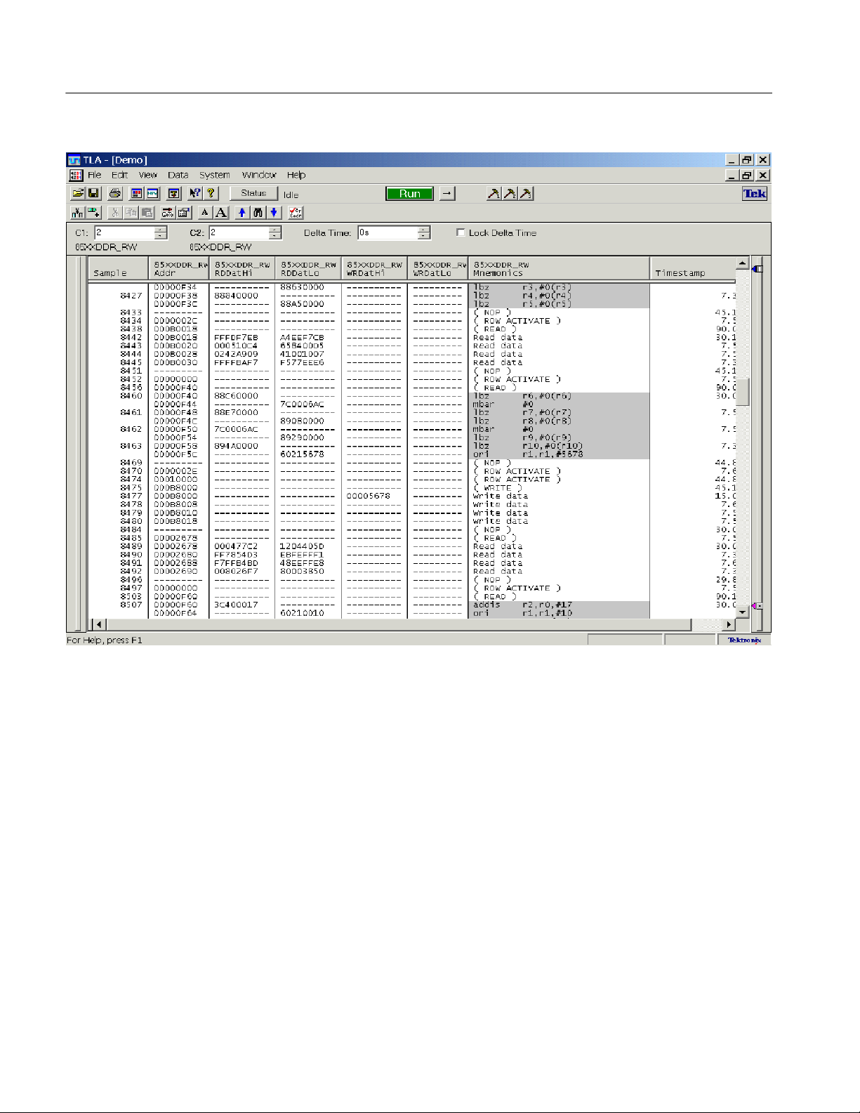
Acquiring and Viewing Disassembled Data
Hardware Display Format
In the hardware display format, all valid opcode fetch bus cycles is disassembled
and displayed. Noninstruction bus cycles are displayed with the appropriate cycle
type labels. This is the default format for disassembly.
Figure 2--2: 85XXDDR hardware display format
TMS568 MPC85XX Microprocessor Software Support
2--15
Page 42
Acquiring and Viewing Disassembled Data
Figure 2--3: 85XXDDR_RW hardware display format
2--16 TMS568 MPC85XX Microprocessor Software Support
Page 43

Acquiring and Viewing Disassembled Data
Figure 2--4: 85XXLB_ALT hardware display format
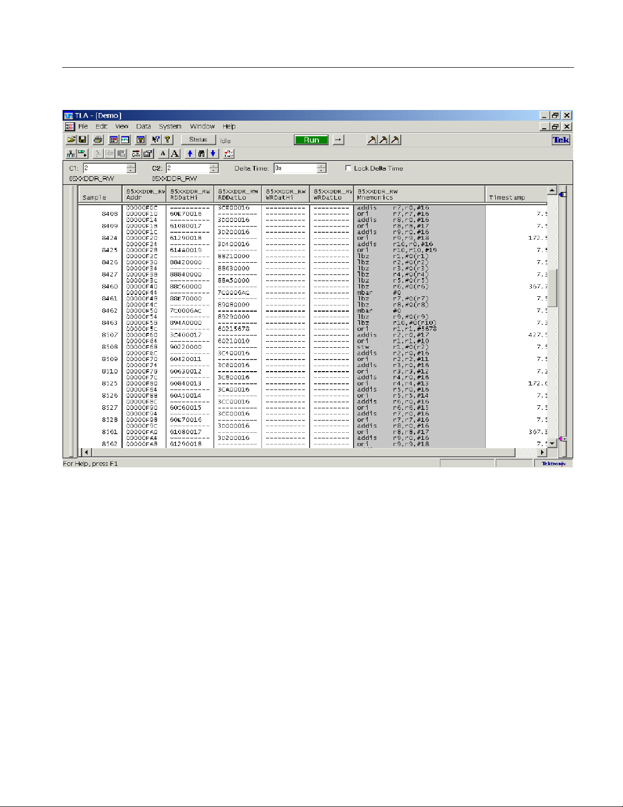
Software Display Format
TMS568 MPC85XX Microprocessor Software Support
In the software display format only the first opcode fetch of executed instruction
cycles is displayed (read extensions are used to disassemble the instruction but
are not displayed as separate cycles in software mode). Noninstruction bus cycles
are not displayed in software mode. Any “special” cycles that are described as
showing up in Control Flow or Subroutine display formats are displayed here.
2--17
Page 44

Acquiring and Viewing Disassembled Data
Figure 2--5: 85XXDDR software display format
2--18 TMS568 MPC85XX Microprocessor Software Support
Page 45
Acquiring and Viewing Disassembled Data
Figure 2--6: 85XXDDR_RW software display format
TMS568 MPC85XX Microprocessor Software Support
2--19
Page 46

Acquiring and Viewing Disassembled Data
Figure 2--7: 85XXLB_ALT software display format
Control Flow Display
Format
2--20 TMS568 MPC85XX Microprocessor Software Support
In Control Flow display format, only the first opcode fetch of instructions that
cause a branch in the addressing is displayed.
b target address ba target address
bl target address bla target address
sc rfi
The following MPC85XX microprocessor instructions conditionally affect
control flow and are displayed if they are taken.
bc BO, BI, target address bca BO, BI, target address
bcl BO, BI, target address bcla BO, BI, target address
bclr BO, BI bclrl BO, BI
bcctr BO, BI bcctrl BO, BI
The following MPC85XX microprocessor instructions are displayed if they cause
an exception to happen (resulting in a change in the control flow).
Page 47

Acquiring and Viewing Disassembled Data
tw twi
sc rfi
Any “special” cycles that are displayed in Subroutine display format are also
displayed here.
Subroutine Display
Format
Marking Cycles
In Subroutine display format, only the first opcode fetch of subroutine call and
return instructions are displayed.
The following MPC85XX microprocessor instructions unconditionally affect
subroutine display:
tw twi isync
The following MPC85XX microprocessor instructions are displayed if they cause
an exception:
sc rfi
The disassembler has a Mark Opcode function that allows you to change the
interpretation of a cycle type. Use this function to select a cycle and change it.
Marks are placed by using the Mark Opcode button. The Mark Opcode button is
always available. When a cycle is marked, the character “>>” is displayed
immediately to the left of the Mnemonics column. Cycles can be unmarked by
using the “Undo Mark” selection, which removes the character “>>”.
If the sample being marked is an Address or SDRAM command cycle, Mark
Opcode selections are replaced by a note indicating that “An Opcode Mark
cannot be placed at the selected data sample”.
Table 2--5 lists Mark selections and definitions for 85XXLB and 85XXLB_ALT
and 85XXLB_ADS support packages.
Table 2--5: Mark selections and definitions in 85XXLB,
85XXLB_ALT, and 85XXLB_ADS
Mark selection or combination Definition
Read-->Fetch Fetch cycle is marked as read cycle
Undo Mark Removes all marks from the current
TMS568 MPC85XX Microprocessor Software Support
sequence
2--21
Page 48

Acquiring and Viewing Disassembled Data
Table 2--6 lists Mark selections and definitions for 85XXDDR and
85XXDDR_RW support packages.
Table 2--6: Mark selections and definitions in 85XXDDR and
85XXDDR_RW
Mark selection or combination Definition
Opcode -- Opcode DataHi or RDDatHi and DataLo or
Opcode -- Flush Only DataHi or RDDatHi is disas-
Flush -- Opcode Only DataHi or RDDatHi is disas-
Flush -- Flush Instructions not disassembled and
Read --> Fetch Read is marked as a Fetch and
Undo Mark Removes all marks from the current
RDDatLo are disassembled
sembled in Big Endian mode and
DataLo or RDDatLo is disassembled
in Little Endian mode
sembled in Little Endian mode and
DataLo or RDDatLo is disassembled
in Big Endian mode
labeled as (Flush)
disassembled
sequence
NOTE. DataHi and DataLo corresponds to 85XXDDR support package.
RDDatHi and RDDatLo corresponds to 85XXDDR_RW support package.
Viewing an Example of Disassembled Data
A demonstration system file (or demonstration reference memory) is provided on
your disk for the three support packages 85XXLB_ALT, 85XXDDR, and
85XXDDR_RW so you can see an example of how your TMS568 MPC85XX
microprocessor bus cycles and instruction mnemonics look when they are
disassembled. Viewing the file system is not a requirement for preparing the
module for use and you can view it without connecting the logic analyzer to your
target system.
Information on basic operations describes how to view the file.
2--22 TMS568 MPC85XX Microprocessor Software Support
Page 49

Reference
Page 50

Page 51

Channel Group Definitions
This section lists the channel group definitions required for disassembly, for the
TMS568 MPC85XX microprocessor support product.
Channel Groups
The software automatically defines channel groups for the support package.
Tables 3--1 through 3--3 show the channel groups for the TMS568 MPC85XX
microprocessor support product for the 85XXDDR, 85XXDDR_RW, 85XXLB,
85XXLB_ALT, and 85XXLB_ADS support packages.
Table 3--1: 85XXDDR support package channel groups
Group name Display radix
Address Hexadecimal
BankAddr Off
DataLo Hexadecimal
DataHi Hexadecimal
Mnemonics Dissasembly generated text
Control Off
Command Off
Strobes Off
ChipSel Off
CheckBits Off
WrtMasks Off
Debug Off
Misc Off
UserDefined Off
DatByte0 Off
DatByte1 Off
DatByte2 Off
DatByte3 Off
DatByte4 Off
DatByte5 Off
DatByte6 Off
TMS568 MPC85XX Microprocessor Software Support
3--1
Page 52

Channel Group Definitions
Table 3--1: 85XXDDR support package channel groups (Cont.)
Group name Display radix
DatByte7 Off
Timestamp
Table 3--2: 85XXDDR_RW support package channel groups
Group name Display radix
Address Hexadecimal
BankAddr Off
RdDatLo Hexadecimal
RdDatHi Hexadecimal
WrDatLo Hexadecimal
WrDatHi Hexadecimal
Mnemonics Dissasembly generated text
Control Off
Command Off
Strobes Off
ChipSel Off
CheckBits Off
WrtMasks Off
Debug Off
Misc Off
UserDefined Off
RDDatBy0 Off
RDDatBy1 Off
RDDatBy2 Off
RDDatBy3 Off
RDDatBy4 Off
RDDatBy5 Off
RDDatBy6 Off
RDDatBy7 Off
WRDatBy0 Off
WRDatBy1 Off
WRDatBy2 Off
WRDatBy3 Off
3--2
TMS568 MPC85XX Microprocessor Software Support
Page 53

Channel Group Definitions
Table 3--2: 85XXDDR_RW support package channel groups (Cont.)
Group name Display radix
WRDatBy4 Off
WRDatBy5 Off
WRDatBy6 Off
WRDatBy7 Off
Timestamp
Table 3--3: 85XXLB, 85XXLB_ALT, 85XXLB_ADS support package
channel groups
Group name Display radix
Address Hexadecimal
BurstAddr Off
Data Hexadecimal
Mnemonics Dissasembly generated text
Control Off
ChipSel Off
Debug Off
DataMask Off
UserDefined Off
Timestamp
TMS568 MPC85XX Microprocessor Software Support
3--3
Page 54

Channel Group Definitions
3--4
TMS568 MPC85XX Microprocessor Software Support
Page 55

Symbol and Channel Assignment Tables
This section lists the symbol tables, channel assignment tables for disassembly
and timing for each of the support packages.
Symbol Tables
The TMS568 MPC85XX microprocessor support product supplies three symbol
table files each for the 85XXLB, 85XXLB_ALT, and 85XXLB_ADS support
packages and two symbol tables each for 85XXDDR and 85XXDDR_RW
support packages.
Tables 3--4 through 3--7 show the definitions for the symbol, bit pattern, and
meaning of the group symbols in the control symbol tables.
Table 3- 4: 85XXLB, 85XXLB_ALT, 85XXLB_ADS ChipSel group symbol
table definitions
ChipSel group value
LCS0~ LCS4~
LCS1~ LCS5~
Symbol
LCS0~ 0111 1111 Chip Select 0
LCS1~ 1011 1111 Chip Select 1
LCS2~ 1101 1111 Chip Select 2
LCS3~ 1110 1111 Chip Select 3
LCS4~ 1111 0111 Chip Select 4
LCS5~ 1111 1011 Chip Select 5
LCS6~ 1111 1101 Chip Select 6
LCS7~ 1111 1110 Chip Select 7
LCS2~ LCS6~
LCS3~ LCS7~
Description
TMS568 MPC85XX Microprocessor Software Support
3- 5
Page 56

Symbol and Channel Assignment Tables
Table 3- 5: 85XXLB, 85XXLB_ALT, 85XXLB_ADS Control group symbol table definitions
Control group value
MDVAL LSDDQM0/LWE0~ LGTA~ LALE
Symbol
Address X XXXX XXX 1XXX Address cycle
SDRAM:Read X XXXX XXX X101 SDRAM Read cycle
SDRAM:Write X XXXX XXX X100 SDRAM Write cycle
SDRAM:Act/
X XXXX XXX X011 SDRAM Activate/
GPCM:Read
SDRAM:Precharge X XXXX XX0 X010 SDRAM Precharge
SDRAM:Precharge--
X XXXX XX1 X010 SDRAM Activate/
all
SDRAM:Auto--
X XXXX XXX X001 SDRAM Precharge
Refresh
SDRAM:Mode--Set X XXXX XXX X000 SDRAM Precharge--
GPCM:LGTA~ X XXXX 0XX XXXX SDRAM Auto--
Write X XXX0 XXX X1XX GPCM Transfer
Write X XX0X XXX X1XX GPCM or SDRAM
Write X X0XX XXX X1XX GPCM or SDRAM
Write X 0XXX XXX X1XX GPCM or SDRAM
DataValid 1 XXXX XXX XXXX Local Bus Data Valid
LSDDQM1/LWE1~ LBCTL LSDRAS~/LBOE~
LSDDQM2/LWE2~ L SDA10/LGPL0 LSDCAS~/LGPL3
LSDDQM3/LWE3~ LSDWE~/LGPL1
Description
GPCM Read cycle
cycle
GPCM
cycle
all cycle
Refresh cycle
Termination
write cycle
write cycle
write cycle
3- 6
TMS568 MPC85XX Microprocessor Software Support
Page 57

Symbol and Channel Assignment Tables
Table 3- 6: 85XXLB, 85XXLB_ALT, 85XXLB_ADS, 85XXDDR, and
85XXDDR_RW Debug group symbol table definitions
Debug group value
MDVAL MSRCID1
MSRCID0 MSRCID2
Symbol
PCI 10 0000
Reserved 10 0001
Reserved 10 0010
Reserved 10 0011
Local Bus 10 0100
Reserved 10 0101
Reserved 10 0110
Reserved 10 0111
Configuration 10 1000
Reserved 10 1001
Boot Sequence 10 1010
Reserved 10 1011
Rapid_IO 10 1100
Reserved 10 1101
Reserved 10 1110
Local_Space (DDR) 10 1111
INSTR_Fetch 11 0000
Data_Fetch 11 0001
Reserved 11 0010
Reserved 11 0011
CPM 11 0100
DMA 11 0101
Reserved 11 0110
SAP 11 0111
Ethernet_0 11 1000
Ethernet_1 11 1001
Ethernet_2 11 1010
Reserved 11 1011
Rapid_IO_Msg 11 1100
Rapid_IO_Doorbell 11 1101
Rapid_IO_Port_Write 11 1110
InValid Port 11 1111
MSRCID3
MSRCID4
TMS568 MPC85XX Microprocessor Software Support
3- 7
Page 58

Symbol and Channel Assignment Tables
Table 3- 7: 85XXDDR AND 85XXDDR_RW Control group symbol table
definitions
Symbol
DESL-IGNORE_COMMAND--DATA? XX11 XXX
NOP-NO OPERATION (S0~) XXX0 1 11
NOP-NO OPERATION (S1~) XX0X 111
BST-BURST STOP (S0~) XXX0 1 10
BST-BURST STOP (S1~) XX0X 110
READ-COL ADDR_READ_(S0~) XXX0 1 0 1
READ-COL_ADDR_READ_(S1~) XX0X 101
WRITE-COL_ADDR_WRITE_(S0~) XXX0 10 0
WRITE-COL_ADDR_WRITE_(S1~) XX0X 10 0
ACTV-ROW_ADDRESS_STROBE_(S0~) XXX0 01 1
PRE-PRECHARGE_SELECT_BANK_(S0~) XXX0 01 0
PRE-PRECHARGE_SELECT_BANK_(S1~) XX0X 010
PALL-PRECHARGE_(S0~) XXX0 01 0
PALL-PRECHARGE_(S1~) XX0X 010
REF-REFRESH_(S0~) XXX0 00 1
REF-REFRESH_(S1~) XX0X 00 1
MRS-MODE_REGISTER_SET_(S0~) XXX0 0 00
MRS-MODE_REG_SET_(S1~) XX0X 0 0 0
Control group value
RESET~ MRAS~
MDVAL MCAS~
CS1~ MWE~
CS0~
Channel Assignment Tables
Channel assignments shown in tables 3--8 through 3--66 use the following
conventions:
H All signals are required by the support package, unless indicated otherwise.
H Channels are shown starting with the most significant bit, descending to the
least significant bit.
H Channel group assignments are for all modules, unless otherwise noted.
3- 8
TMS568 MPC85XX Microprocessor Software Support
Page 59

Symbol and Channel Assignment Tables
85XXDDR Channel Group
Assignments
Tables 3--8 through 3--28 show the channel assignments for the logic analyzer
groups for the 85XXDDR support package and the microprocessor signal to
which each channel connects.
Table 3--8 lists the channel assignments for the Address group and the microprocessor signal to which each channel connects. By default, this channel group is
displayed in hexadecimal.
Table 3- 8: Address group assignments for 85XXDDR support package
85XXDDR support package
Bit order Section:Channel
14 (MSB) C3:2 MA14
13 C3:7 MA13
12 D1:4 MA12
11 D2:1 MA11
10 E2:0 MA10
9 A2:1 MA9
8 A2:4 MA8
7 D2:3 MA7
channel name
6 D3:0 MA6
5 D2:6 MA5
4 D3:1 MA4
3 D3:2 MA3
2 A3:3 MA2
1 A3:5 MA1
0 (LSB) E0:0 MA0
Table 3--9 lists the channel assignments for the BankAddr group and the
microprocessor signal to which each channel connects. By default, this channel
group is not displayed.
Table 3- 9: BankAddr group assignments for 85XXDDR support package
85XXDDR support package
Bit order Section:Channel
2 (MSB) E2:7 MBA0
1 E0:3 MBA1
0 (LSB) D1:7 MBA2
channel name
TMS568 MPC85XX Microprocessor Software Support
3- 9
Page 60

Symbol and Channel Assignment Tables
Table 3--10 lists the channel assignments for the DataLo group and the microprocessor signal to which each channel connects. By default, this group is displayed
in hexadecimal.
Table 3- 10: DataLo group assignments for 85XXDDR support package
Bit order Section:Channel
31 (MSB) D0:0 MDQ0
30 D0:1 MDQ1
29 A0:2 MDQ2
28 D0:4 MDQ3
27 A0:0 MDQ4
26 A0:1 MDQ5
25 A0:4 MDQ6
24 A0:3 MDQ7
85XXDDR support package
channel name
23 A0:7 MDQ8
22 D0:7 MDQ9
21 A1:1 MDQ10
20 D1:2 MDQ11
19 A1:2 MDQ12
18 A1:6 MDQ13
17 A1:5 MDQ14
16 A1:4 MDQ15
15 D1:1 MDQ16
14 D1:5 MDQ17
13 D2:4 MDQ18
12 D2:5 MDQ19
11 D1:3 MDQ20
10 A2:0 MDQ21
9 A2:2 MDQ22
8 A2:3 MDQ23
7 A2:5 MDQ24
3- 10
6 D2:7 MDQ25
5 A3:2 MDQ26
4 A3:4 MDQ27
3 A2:6 MDQ28
TMS568 MPC85XX Microprocessor Software Support
Page 61

Symbol and Channel Assignment Tables
Table 3- 10: DataLo group assignments for 85XXDDR support package (Cont.)
85XXDDR support package
Bit order
2 A3:0 MDQ29
1 D3:4 MDQ30
0 (LSB) D3:3 MDQ31
Section:Channel
channel name
Table 3--11 lists the channel assignments for the DataHi group and the microprocessor signal to which each channel connects. By default, this group is displayed
in hexadecimal.
Table 3- 11: DataHi group assignments for 85XXDDR support package
85XXDDR support package
Bit order Section:Channel
31 (MSB) E2:4 MDQ32
channel name
30 E0:5 MDQ33
29 E2:6 MDQ34
28 E3:1 MDQ35
27 E2:3 MDQ36
26 E2:5 MDQ37
25 E0:7 MDQ38
24 E3:0 MDQ39
23 E3:2 MDQ40
22 E3:3 MDQ41
21 E1:3 MDQ42
20 E1:6 MDQ43
19 E3:4 MDQ44
18 E3:6 MDQ45
17 E1:7 MDQ46
16 E1:2 MDQ47
15 E1:5 MDQ48
14 C0:0 MDQ49
13 C0:5 MDQ50
12 C3:4 MDQ51
11 C0:1 MDQ52
TMS568 MPC85XX Microprocessor Software Support
3- 11
Page 62

Symbol and Channel Assignment Tables
Table 3- 11: DataHi group assignments for 85XXDDR support package (Cont.)
Bit order
10 C0:2 MDQ53
9 C3:3 MDQ54
8 C0:3 MDQ55
7 C2:7 MDQ56
6 C3:0 MDQ57
5 C1:1 MDQ58
4 C1:2 MDQ59
3 C1:0 MDQ60
2 C3:1 MDQ61
1 C2:5 MDQ62
0 (LSB) C2:4 MDQ63
Section:Channel
85XXDDR support package
channel name
Table 3--12 lists the channel assignments for the Control group and the microprocessor signal to which each channel connects. By default, this group is not
displayed.
Table 3- 12: Control group assignments for 85XXDDR support package
85XXDDR support package
Bit order Section:Channel
6 (MSB) A0:6 RESET~
5 Qual:0 MDVAL
4 C2:0 MCS1~
3 C2:3 MCS0~
2 C2:2 MRAS~
1 C2:1 MCAS~
0 (LSB) Qual:3 MWE~
channel name
3- 12
TMS568 MPC85XX Microprocessor Software Support
Page 63

Symbol and Channel Assignment Tables
Table 3--13 lists the channel assignments for the command group and the
microprocessor signal to which each channel connects. By default, this group is
not displayed.
Table 3- 13: Command group assignments for 85XXDDR support packages
85XXDDR support package
Bit order Section:Channel
4 (MSB) C2:0 MCS1~
3 C2:3 MCS0~
2 C2:2 MRAS~
1 C2:1 MCAS~
0 (LSB) Qual:3 MWE~
channel name
Table 3--14 lists the channel assignments for the Strobes group and the microprocessor signal to which each channel connects. By default, this group is not
displayed.
Table 3- 14: Strobes group assignments for 85XXDDR support package
85XXDDR support package
Bit order Section:Channel
7 (MSB) D0:2 MDQS0
6 A1:3 MDQS1
5 D2:0 MDQS2
4 A2:7 MDQS3
3 E0:6 MDQS4
2 E3:5 MDQS5
1 C3:5 MDQS6
0 (LSB) C2:6 MDQS7
channel name
TMS568 MPC85XX Microprocessor Software Support
3- 13
Page 64

Symbol and Channel Assignment Tables
Table 3--15 lists the channel assignments for the ChipSel group and the
microprocessor signal to which each channel connects. By default, this group is
not displayed.
Table 3- 15: ChipSel group assignments for 85XXDDR support package
Bit order Section:Channel
3 (MSB) C2:3 MCS0~
2 C2:0 MCS1~
1 E1:1 MCS2~
0 (LSB) E1:4 MCS3~
Table 3--16 lists the channel assignments for the CheckBits group and the
microprocessor signal to which each channel connects. By default, this group is
not displayed.
85XXDDR support package
channel name
Table 3- 16: CheckBits group assignments for 85XXDDR support package
85XXDDR support package
Bit order Section:Channel
7 D3:6 ECC0
6 A3:7 ECC1
5 E0:2 ECC2
4 E2:1 ECC3
3 D3:5 ECC4
2 A3:6 ECC5
1 E0:4 ECC6
0 E2:2 ECC7
channel name
Table 3--17 lists the channel assignments for the WrtMasks group assignments
for the 85XXDDR support package. By default, this group is not displayed.
Table 3- 17: WrtMasks group assignments for 85XXDDR support package
85XXDDR support package
Bit order Section:Channel
7 (MSB) D0:3 MDM0
channel name
3- 14
6 A1:7 MDM1
TMS568 MPC85XX Microprocessor Software Support
Page 65

Symbol and Channel Assignment Tables
Table 3- 17: WrtMasks group assignments for 85XXDDR support package (Cont.)
85XXDDR support package
Bit order
5 D2:2 MDM2
4 A3:1 MDM3
3 E1:0 MDM4
2 E3:7 MDM5
1 C3:6 MDM6
0 (LSB) C0:7 MDM7
Section:Channel
channel name
Table 3--18 lists the channel assignments for the Debug group and the microprocessor signal to which each channel connects. By default, this group is not
displayed.
Table 3- 18: Debug group assignments for the 85XXDDR support package
85XXDDR support package
Bit order Section: Channel
4 (MSB) A0:5 MSRCID0
3 Clock:2 MSRCID1
2 D1:0 MSRCID2
1 D0:6 MSRCID3
0 (LSB) D0:5 MSRCID4
channel name
Table 3--19 lists the channel assignments for the Misc group and the microprocessor signal to which each channel connects. By default, this group is not
displayed.
Table 3- 19: Misc group assignments for 85XXDDR support package
85XXDDR support package
Bit order Section: Channel
2 (MSB) Clock:0 MCK0
1 Clock:1 MCK1
0 (LSB) Clock:3 MCK2
channel name
TMS568 MPC85XX Microprocessor Software Support
3- 15
Page 66

Symbol and Channel Assignment Tables
Table 3--20 lists the channel assignments for the UserDefined group and the
microprocessor signal to which each channel connects. By default, this group is
not displayed.
Table 3- 20: UserDefined group assignments for the 85XXDDR support
package
Bit order Section: Channel
12 (MSB) Qual:2 NC--No signal
11 Qual:1 SCL
10 D1:6 MCKE0
9 A1:0 MCKE1
8 C1:4 SA0
7 C1:6 SA1
6 C1:5 SA2
85XXDDR support package
channel name
5 C1:7 SDA
4 C0:6 VDDID
3 C1:3 TRIG_IN
2 C0:4 TRIG_OUT
1 E0:1 DM8
0 (LSB) D3:7 DQS8
Table 3--21 lists the channel assignments for the DatByte0 group and the
microprocessor signal to which each channel connects. By default, this group is
not displayed.
Table 3- 21: DatByte0 group assignments for 85XXDDR support package
85XXDDR support package
Bit order Section: Channel
8 (MSB) D0:3 MDM0
7 D0:0 MDQ0
6 D0:1 MDQ1
5 A0:2 MDQ2
channel name
3- 16
4 D0:4 MDQ3
3 A0:0 MDQ4
2 A0:1 MDQ5
TMS568 MPC85XX Microprocessor Software Support
Page 67

Symbol and Channel Assignment Tables
Table 3- 21: DatByte0 group assignments for 85XXDDR support package (Cont.)
85XXDDR support package
Bit order
1 A0:4 MDQ6
0 (LSB) A0:3 MDQ7
Section: Channel
channel name
Table 3--22 lists the channel assignments for the DatByte1 group and the
microprocessor signal to which each channel connects. By default, this group is
not displayed.
Table 3- 22: DatByte1 group assignments for 85XXDDR support package
85XXDDR support package
Bit order Section: Channel
8 (MSB) A1:7 MDM1
7 A0:7 MDQ8
channel name
6 D0:7 MDQ9
5 A1:1 MDQ10
4 D1:2 MDQ11
3 A1:2 MDQ12
2 A1:6 MDQ13
1 A1:5 MDQ14
0 (LSB) A1:4 MDQ15
Table 3--23 lists the channel assignments for the DatByte2 user defined group
and the microprocessor signal to which each channel connects. By default, this
group is not displayed.
Table 3- 23: DatByte2 group assignments for 85XXDDR support package
85XXDDR support package
Bit order Section: Channel
8 (MSB) D2:2 MDM2
7 D1:1 MDQ16
6 D1:5 MDQ17
channel name
5 D2:4 MDQ18
4 D2:5 MDQ19
3 D1:3 MDQ20
TMS568 MPC85XX Microprocessor Software Support
3- 17
Page 68

Symbol and Channel Assignment Tables
Table 3- 23: DatByte2 group assignments for 85XXDDR support package (Cont.)
Bit order
2 A2:0 MDQ21
1 A2:2 MDQ22
0 (LSB) A2:3 MDQ23
Table 3--24 lists the channel assignments for the DatByte3 group and the
microprocessor signal to which each channel connects. By default, this group is
not displayed.
Table 3- 24: DatByte3 group assignments for 85XXDDR support package
Bit order Section: Channel
8 A3:1 MDM3
Section: Channel
85XXDDR support package
channel name
85XXDDR support package
channel name
7 A2:5 MDQ24
6 D2:7 MDQ25
5 A3:2 MDQ26
4 A3:4 MDQ27
3 A2:6 MDQ28
2 A3:0 MDQ29
1 D3:4 MDQ30
0 D3:3 MDQ31
Table 3--25 lists the channel assignments for the DatByte4 group and the
microprocessor signal to which each channel connects. By default, this group is
not displayed.
Table 3- 25: DatByte4 group assignments for 85XXDDR support package
85XXDDR support package
Bit order Section: Channel
8 (MSB) E1:0 MDM4
7 E2:4 MDQ32
channel name
3- 18
6 E0:5 MDQ33
5 E2:6 MDQ34
4 E3:1 MDQ35
TMS568 MPC85XX Microprocessor Software Support
Page 69

Symbol and Channel Assignment Tables
Table 3- 25: DatByte4 group assignments for 85XXDDR support package (Cont.)
85XXDDR support package
Bit order
3 E2:3 MDQ36
2 E2:5 MDQ37
1 E0:7 MDQ38
0 (LSB) E3:0 MDQ39
Section: Channel
channel name
Table 3--26 lists the channel assignments for the DatByte5 group and the
microprocessor signal to which each channel connects. By default, this group is
not displayed.
Table 3- 26: DatByte5 group assignments for 85XXDDR support package
85XXDDR support package
Bit order Section: Channel
8 (MSB) E3:7 MDM5
channel name
7 E3:2 MDQ40
6 E3:3 MDQ41
5 E1:3 MDQ42
4 E1:6 MDQ43
3 E3:4 MDQ44
2 E3:6 MDQ45
1 E1:7 MDQ46
0 (LSB) E1:2 MDQ47
Table 3--27 lists the channel assignments for the DatByte6 group and the
microprocessor signal to which each channel connects. By default, this group is
not displayed.
Table 3- 27: DatByte6 group assignments for 85XXDDR support package
85XXDDR support package
Bit order Section: Channel
8 (MSB) C3:6 MDM6
7 E1:5 MDQ48
channel name
6 C0:0 MDQ49
5 C0:5 MDQ50
TMS568 MPC85XX Microprocessor Software Support
3- 19
Page 70

Symbol and Channel Assignment Tables
Table 3- 27: DatByte6 group assignments for 85XXDDR support package (Cont.)
Bit order
4 C3:4 MDQ51
3 C0:1 MDQ52
2 C0:2 MDQ53
1 C3:3 MDQ54
0 (LSB) C0:3 MDQ55
Table 3--28 lists the channel assignments for the DatByte7 group and the
microprocessor signal to which each channel connects. By default, this group is
not displayed.
Table 3- 28: DatByte7 group assignments for 85XXDDR support package
Section: Channel
85XXDDR support package
channel name
85XXDDR support package
Bit order Section: Channel
8 (MSB) C0:7 MDM7
7 C2:7 MDQ56
6 C3:0 MDQ57
5 C1:1 MDQ58
4 C1:2 MDQ59
3 C1:0 MDQ60
2 C3:1 MDQ61
1 C2:5 MDQ62
0 (LSB) C2:4 MDQ63
channel name
3- 20
TMS568 MPC85XX Microprocessor Software Support
Page 71

Symbol and Channel Assignment Tables
85XXDDR_RW Channel
Group Assignments
Tables 3--29 through 3--59 list the channel assignments for the logic analyzer
groups for the 85XXDDR_RW support package.
Table 3--29 lists the Address group assignments for the 85XXDDR_RW support
package. By default, this group is displayed in hexadecimal.
Table 3- 29: Address group assignments for 85XXDDR_RW support
package
85XXDDR_RW support
Bit order Section: Channel
14 (MSB) $0_C3:2 MA14
13 $0_C3:7 MA13
12 $1_E3:4 MA12
11 $1_C2:1 MA11
10 $0_E2:0 MA10
9 $0_A2:1 MA9
8 $0_A2:4 MA8
7 $1_C2:3 MA7
6 $1_C3:0 MA6
package channel name
5 $1_C2:6 MA5
4 $1_C3:1 MA4
3 $1_C3:2 MA3
2 $0_A3:3 MA2
1 $0_A3:5 MA1
0 (LSB) $1_A2:0 MA0
Table 3--30 lists the channel assignments for the BankAddr group and the
microprocesser signal to which each channel connects. By default, this group is
not displayed.
Table 3- 30: BankAddr group assignments for 85XXDDR_RW support
package
85XXDDR_RW support
Bit order Section: Channel
2 (MSB) $0_E2:7 MBA0
1 $1_A2:3 MBA1
0 (LSB) $1_E3:7 MBA2
package channel name
TMS568 MPC85XX Microprocessor Software Support
3- 21
Page 72

Symbol and Channel Assignment Tables
Table 3--31 lists the channel assignments for the RdDatLo group and the
microprocesser signal to which each channel connects. By default, this group is
displayed in hexadecimal.
Table 3- 31: RdDatLo group assignments for 85XXDDR_RW support
package
Bit order Section:Channel
31 (MSB) $1_E2:0 MDQ0
30 $1_E2:1 MDQ1
29 $0_A0:2 MDQ2
28 $1_E2:4 MDQ3
27 $0_A0:0 MDQ4
26 $0_A0:1 MDQ5
25 $0_A0:4 MDQ6
85XXDDR_RW support
package channel name
24 $0_A0:3 MDQ7
23 $0_A0:7 MDQ8
22 $1_E2:7 MDQ9
21 $0_A1:1 MDQ10
20 $1_E3:2 MDQ11
19 $0_A1:2 MDQ12
18 $0_A1:6 MDQ13
17 $0_A1:5 MDQ14
16 $0_A1:4 MDQ15
15 $1_E3:1 MDQ16
14 $1_E3:5 MDQ17
13 $1_C2:4 MDQ18
12 $1_C2:5 MDQ19
11 $1_E3:3 MDQ20
10 $0_A2:0 MDQ21
9 $0_A2:2 MDQ22
8 $0_A2:3 MDQ23
3- 22
7 $0_A2:5 MDQ24
6 $1_C2:7 MDQ25
5 $0_A3:2 MDQ26
4 $0_A3:4 MDQ27
TMS568 MPC85XX Microprocessor Software Support
Page 73

Symbol and Channel Assignment Tables
Table 3- 31: RdDatLo group assignments for 85XXDDR_RW support
package (Cont.)
85XXDDR_RW support
Bit order
3 $0_A2:6 MDQ28
2 $0_A3:0 MDQ29
1 $1_C3:4 MDQ30
0 (LSB) $1_C3:3 MDQ31
Section:Channel
package channel name
Table 3--32 lists the channel assignments for the RdDatHi group and the
microprocessor signal to which each channel connects. By default, this group is
displayed in hexadecimal.
Table 3- 32: RdDatHi group assignments for 85XXDDR_RW support
package
85XXDDR_RW support pack-
Bit order Section:Channel
31(MSB) $0_E2:4 MDQ32
30 $1_A2:5 MDQ33
29 $0_E2:6 MDQ34
28 $0_E3:1 MDQ35
27 $0_E2:3 MDQ36
26 $0_E2:5 MDQ37
25 $1_A2:7 MDQ38
24 $0_E3:0 MDQ39
23 $0_E3:2 MDQ40
22 $0_E3:3 MDQ41
21 $1_A3:3 MDQ42
20 $1_A3:6 MDQ43
19 $0_E3:4 MDQ44
18 $0_E3:6 MDQ45
17 $1_A3:7 MDQ46
16 $1_A3:2 MDQ47
age channel name
15 $1_A3:5 MDQ48
14 $1_A0:0 MDQ49
13 $1_A0:5 MDQ50
TMS568 MPC85XX Microprocessor Software Support
3- 23
Page 74

Symbol and Channel Assignment Tables
Table 3- 32: RdDatHi group assignments for 85XXDDR_RW support
package (Cont.)
Bit order
12 $0_C3:4 MDQ51
11 $1_A0:1 MDQ52
10 $1_A0:2 MDQ53
9 $0_C3:3 MDQ54
8 $1_A0:3 MDQ55
7 $0_C2:7 MDQ56
6 $0_C3:0 MDQ57
5 $1_A1:1 MDQ58
4 $1_A1:2 MDQ59
3 $1_A1:0 MDQ60
Section:Channel
85XXDDR_RW support package channel name
2 $0_C3:1 MDQ61
1 $0_C2:5 MDQ62
0 (LSB) $0_C2:4 MDQ63
Table 3--33 lists the channel assignments for the WrDatLo group and the
microprocessor signal to which each channel connects. By default, this group is
displayed in hexadecimal.
Table 3- 33: WrDatLo group assignments for 85XXDDR_RW support
package
85XXDDR_RW support
Bit order Section:Channel
31 (MSB) $1_E0:0 MDQ0_DM
30 $1_E0:1 MDQ1_DM
29 $0_D0:2 MDQ2_DM
28 $1_E0:4 MDQ3_DM
27 $0_D0:0 MDQ4_DM
26 $0_D0:1 MDQ5_DM
package channel name
3- 24
25 $0_D0:4 MDQ6_DM
24 $0_D0:3 MDQ7_DM
23 $0_D0:7 MDQ8_DM
22 $1_E0:7 MDQ9_DM
TMS568 MPC85XX Microprocessor Software Support
Page 75

Symbol and Channel Assignment Tables
Table 3- 33: WrDatLo group assignments for 85XXDDR_RW support
package (Cont.)
85XXDDR_RW support
Bit order
21 $0_D1:1 MDQ10_DM
20 $1_E1:2 MDQ11_DM
19 $0_D1:2 MDQ12_DM
18 $0_D1:6 MDQ13_DM
17 $0_D1:5 MDQ14_DM
16 $0_D1:4 MDQ15_DM
15 $1_E1:1 MDQ16_DM
14 $1_E1:5 MDQ17_DM
13 $1_C0:4 MDQ18_DM
12 $1_C0:5 MDQ19_DM
Section:Channel
package channel name
11 $1_E1:3 MDQ20_DM
10 $0_D2:0 MDQ21_DM
9 $0_D2:2 MDQ22_DM
8 $0_D2:3 MDQ23_DM
7 $0_D2:5 MDQ24_DM
6 $1_C0:7 MDQ25_DM
5 $0_D3:2 MDQ26_DM
4 $0_D3:4 MDQ27_DM
3 $0_D2:6 MDQ28_DM
2 $0_D3:0 MDQ29_DM
1 $1_C1:4 MDQ30_DM
0 (LSB) $1_C1:3 MDQ31_DM
TMS568 MPC85XX Microprocessor Software Support
3- 25
Page 76

Symbol and Channel Assignment Tables
Table 3--34 lists the channel assignments for the WrDatHi group and the
microprocessor signal to which each channel connects. By default, this group is
displayed in hexadecimal.
Table 3- 34: WrDatHi group assignments for 85XXDDR_RW support
package
Bit order Section:Channel
31 (MSB) $0_E0:4 MDQ32_DM
30 $1_D2:5 MDQ33_DM
29 $0_E0:6 MDQ34_DM
28 $0_E1:1 MDQ35_DM
27 $0_E0:3 MDQ36_DM
26 $0_E0:5 MDQ37_DM
25 $1_D2:7 MDQ38_DM
85XXDDR_RW support
package channel name
24 $0_E1:0 MDQ39_DM
23 $0_E1:2 MDQ40_DM
22 $0_E1:3 MDQ41_DM
21 $1_D3:3 MDQ42_DM
20 $1_D3:6 MDQ43_DM
19 $0_E1:4 MDQ44_DM
18 $0_E1:6 MDQ45_DM
17 $1_D3:7 MDQ46_DM
16 $1_D3:2 MDQ47_DM
15 $1_D3:5 MDQ48_DM
14 $1_D0:0 MDQ49_DM
13 $1_D0:5 MDQ50_DM
12 $0_C1:4 MDQ51_DM
11 $1_D0:1 MDQ52_DM
10 $1_D0:2 MDQ53_DM
9 $0_C1:3 MDQ54_DM
8 $1_D0:3 MDQ55_DM
3- 26
7 $0_C0:7 MDQ56_DM
6 $0_C1:0 MDQ57_DM
5 $1_D1:1 MDQ58_DM
4 $1_D1:2 MDQ59_DM
TMS568 MPC85XX Microprocessor Software Support
Page 77
Symbol and Channel Assignment Tables
Table 3- 34: WrDatHi group assignments for 85XXDDR_RW support
package (Cont.)
85XXDDR_RW support
Bit order
3 $1_D1:0 MDQ60_DM
2 $0_C1:1 MDQ61_DM
1 $0_C0:5 MDQ62_DM
0 (LSB) $0_C0:4 MDQ63_DM
Section:Channel
package channel name
Table 3--35 lists the channel assignments for the Control group and the microprocessor signal to which each channel connects. By default, this group is not
displayed.
Table 3- 35: Control group assignments for 85XXDDR_RW support package
85XXDDR_RW support
Bit order Section:Channel
6 (MSB) $0_A0:6 RESET~
5 $1_Clock:3 MDVAL
4 $0_C2:0 MCSI~
3 $0_C2:3 MCS0~
2 $0_C2:2 MRAS~
1 $0_C2:1 MCAS~
0 (LSB) $0_Qual:3 MWE~
package channel name
Table 3--36 lists the channel assignments for the Command group and the
microprocessor signal to which each channel connects. By default, this group is
displayed in symbols.
Table 3- 36: Command group assignments for 85XXDDR_RW support
package
85XXDDR_RW support
Bit order Section: Channel
4 (MSB) $0_C2:0 MCS1~
package channel name
3 $0_C2:3 MCS0~
2 $0_C2:2 MRAS~
TMS568 MPC85XX Microprocessor Software Support
3- 27
Page 78

Symbol and Channel Assignment Tables
Table 3- 36: Command group assignments for 85XXDDR_RW support
package (Cont.)
Bit order
1 $0_C2:1 MCAS~
0 (LSB) $0_Qual:3 MWE~
Table 3--37 lists the channel assignments for the Strobes group and the microprocessor signal to which each channel connects. By default, this group is displayed
in symbols.
Table 3- 37: Strobes group assignments for 85XXDDR_RW support
package
Bit order Section:Channel
7 (MSB) $1_E2:2 MDQS0
Section: Channel
85XXDDR_RW support
package channel name
85XXDDR_RW support
package channel name
6 $0_A1:3 MDQS1
5 $1_C2:0 MDQS2
4 $0_A2:7 MDQS3
3 $1_A2:6 MDQS4
2 $0_E3:5 MDQS5
1 $0_C3:5 MDQS6
0 (LSB) $0_C2:6 MDQS7
Table 3--38 lists the channel assignments for the ChipSel group and the
microprocessor signal to which each channel connects. By default, this group is
displayed in symbols.
Table 3- 38: ChipSel assignments for 85XXDDR_RW support package
85XXDDR_RW support
Bit order Section:Channel
3 (MSB) $0_C2:3 MCS0~
2 $0_C2:0 MCS1~
1 $1_A3:1 MCS2~
package channel name
3- 28
0 (LSB) $1_A3:4 MCS3~
TMS568 MPC85XX Microprocessor Software Support
Page 79

Symbol and Channel Assignment Tables
Table 3--39 lists the channel assignments for the CheckBits group and the
microprocessor signal to which each channel connects. By default, this group is
not displayed.
Table 3- 39: CheckBits group assignments for 85XXDDR_RW support
package
85XXDDR_RW support
Bit order Section:Channel
7 (MSB) $1_C3:6 ECC0
6 $0_A3:7 ECC1
5 $1_A2:2 ECC2
4 $0_E2:1 ECC3
3 $1_C3:5 ECC4
2 $0_A3:6 ECC5
1 $1_A2:4 ECC6
package channel name
0 (LSB) $0_E2:2 ECC7
Table 3--40 lists the channel assignments for the WrtMasks group and the
microprocessor signal to which each channel connects. By default, this group is
not displayed.
Table 3- 40: WrtMasks group assignments for 85XXDDR_RW support
package
85XXDDR_RW support
Bit order Section:Channel
7 (MSB) $1_E2:3 MDM0
6 $0_A1:7 MDM1
5 $1_C2:2 MDM2
4 $0_A3:1 MDM3
3 $1_A3:0 MDM4
2 $0_E3:7 MDM5
1 $0_C3:6 MDM6
0 (LSB) $1_A0:7 MDM7
package channel name
TMS568 MPC85XX Microprocessor Software Support
3- 29
Page 80

Symbol and Channel Assignment Tables
Table 3--41 lists the channel assignments for the Debug group and the microprocessor signal to which each channel connects. By default, this group is not
displayed.
Table 3- 41: Debug group assignments for 85XXDDR_RW support package
Bit order Section:Channel
4 (MSB) $0_A0:5 MSRCID0
3 $1_Qual:3 MSRCID1
2 $1_E3:0 MSRCID2
1 $1_E2:6 MSRCID3
0 (LSB) $1_E2:5 MSRCID4
Table 3--42 lists the channel assignments for the Misc group and the microprocessor signal to which each channel connects. By default, this group is not
displayed.
85XXDDR_RW support
package channel name
Table 3- 42: Misc group assignments for 85XXDDR_RW support package
85XXDDR_RW support
Bit order Section:Channel
2 (MSB) $0_Clock:3 MCK2
1 $0_Clock:1 MCK1
0 (LSB) $0_Clock:0 MCK0
package channel name
Table 3--43 lists the channel assignments for the UserDefined group and the
microprocessor signal to which each channel connects. By default, this group is
not displayed.
Table 3- 43: UserDefined group assignments for 85XXDDR_RW support
package
85XXDDR_RW support
Bit order Section:Channel
12 (MSB) $1_Clock:0 NC--No signal
11 $1_Clock:1 SCL
10 $1_E3:6 MCKE0
package channel name
3- 30
9 $0_A1:0 MCKE1
8 $1_A1:4 SA0
TMS568 MPC85XX Microprocessor Software Support
Page 81

Symbol and Channel Assignment Tables
Table 3- 43: UserDefined group assignments for 85XXDDR_RW support
package (Cont.)
85XXDDR_RW support
Bit order
7 $1_A1:6 SA1
6 $1_A1:5 SA2
5 $1_A1:7 SDA
4 $1_A0:6 VDDID
3 $1_A1:3 TRIG_IN
2 $1_A0:4 TRIG_OUT
1 $1_A2:1 NC_DM8
0 (LSB) $1_C3:7 NC_DQS8
Section:Channel
package channel name
Table 3--44 lists the channel assignments for the RDDatBy0 group and the
microprocessor signal to which each channel connects. By default, this group is
not displayed.
Table 3- 44: RDDatBy0 group assignments for 85XXDDR_RW support
package
85XXDDR_RW support
Bit order Section:Channel
7 $1_E2:0 MDQ0
6 $1_E2:1 MDQ1
5 $0_A0:2 MDQ2
4 $1_E2:4 MDQ3
3 $0_A0:0 MDQ4
2 $0_A0:1 MDQ5
1 $0_A0:4 MDQ6
0 (LSB) $0_A0:3 MDQ7
package channel name
TMS568 MPC85XX Microprocessor Software Support
3- 31
Page 82

Symbol and Channel Assignment Tables
Table 3--45 lists the channel assignments for the RDDatBy1 group and the
microprocessor signal to which each channel connects. By default, this group is
not displayed.
Table 3- 45: RDDatBy1 group assignments for 85XXDDR_RW support
package
Bit order Section:Channel
7 $0_A0:7 MDQ8
6 $1_E2:7 MDQ9
5 $0_A1:1 MDQ10
4 $1_E3:2 MDQ11
3 $0_A1:2 MDQ12
2 $0_A1:6 MDQ13
1 $0_A1:5 MDQ14
85XXDDR_RW support
package channel name
0 (LSB) $0_A1:4 MDQ15
Table 3--46 lists the channel assignments for the RDDatBy2 group and the
microprocessor signal to which each channel connects. By default, this group is
not displayed.
Table 3- 46: RDDatBy2 group assignments for 85XXDDR_RW support
package
85XXDDR_RW support
Bit order Section:Channel
7 $1_E3:1 MDQ16
6 $1_E3:5 MDQ17
5 $1_C2:4 MDQ18
4 $1_C2:5 MDQ19
3 $1_E3:3 MDQ20
2 $0_A2:0 MDQ21
1 $0_A2:2 MDQ22
0 (LSB) $0_A2:3 MDQ23
package channel name
3- 32
TMS568 MPC85XX Microprocessor Software Support
Page 83

Symbol and Channel Assignment Tables
Table 3--47 lists the channel assignments for the RDDatBy3 group and the
microprocessor signal to which each channel connects. By default, this group is
not displayed.
Table 3- 47: RDDatBy3 group assignments for 85XXDDR_RW support
package
85XXDDR_RW support
Bit order Section:Channel
7 $0_A2:5 MDQ24
6 $1_C2:7 MDQ25
5 $0_A3:2 MDQ26
4 $0_A3:4 MDQ27
3 $0_A2:6 MDQ28
2 $0_A3:0 MDQ29
1 $1_C3:4 MDQ30
package channel name
0 (LSB) $1_C3:3 MDQ31
Table 3--48 lists the channel assignments for the RDDatBy4 group and the
microprocessor signal to which each channel connects. By default, this group is
not displayed.
Table 3- 48: RDDatBy4 group assignments for 85XXDDR_RW support
package
85XXDDR_RW support
Bit order Section:Channel
7 $0_E2:4 MDQ32
6 $1_A2:5 MDQ33
5 $0_E2:6 MDQ34
4 $0_E3:1 MDQ35
3 $0_E2:3 MDQ36
2 $0_E2:5 MDQ37
1 $1_A2:7 MDQ38
0 (LSB) $0_E3:0 MDQ39
package channel name
TMS568 MPC85XX Microprocessor Software Support
3- 33
Page 84

Symbol and Channel Assignment Tables
Table 3--49 lists the channel assignments for the RDDatBy5 group and the
microprocessor signal to which each channel connects. By default, this group is
not displayed.
Table 3- 49: RDDatBy5 group assignments for 85XXDDR_RW support
package
Bit order Section:Channel
7 $0_E3:2 MDQ40
6 $0_E3:3 MDQ41
5 $1_A3:3 MDQ42
4 $1_A3:6 MDQ43
3 $0_E3:4 MDQ44
2 $0_E3:6 MDQ45
1 $1_A3:7 MDQ46
85XXDDR_RW support
package channel name
0 (LSB) $1_A3:2 MDQ47
Table 3--50 lists the channel assignments for the RDDatBy6 group and the
microprocessor signal to which each channel connects. By default, this group is
not displayed.
Table 3- 50: RDDatBy6 group assignments for 85XXDDR_RW support
package
85XXDDR_RW support
Bit order Section:Channel
7 $1_A3:5 MDQ48
6 $1_A0:0 MDQ49
5 $1_A0:5 MDQ50
4 $0_C3:4 MDQ51
3 $1_A0:1 MDQ52
2 $1_A0:2 MDQ53
1 $0_C3:3 MDQ54
0 (LSB) $1_A0:3 MDQ55
package channel name
3- 34
TMS568 MPC85XX Microprocessor Software Support
Page 85

Symbol and Channel Assignment Tables
Table 3--51 lists the channel assignments for the RDDatBy7 group and the
microprocessor signal to which each channel connects. By default, this group is
not displayed.
Table 3- 51: RDDatBy7 group assignments for 85XXDDR_RW support
package
85XXDDR_RW support
Bit order Section:Channel
7 $0_C2:7 MDQ56
6 $0_C3:0 MDQ57
5 $1_A1:1 MDQ58
4 $1_A1:2 MDQ59
3 $1_A1:0 MDQ60
2 $0_C3:1 MDQ61
1 $0_C2:5 MDQ62
package channel name
0 (LSB) $0_C2:4 MDQ63
Table 3--52 lists the channel assignments for the WRDatBy0 group and the
microprocessor signal to which each channel connects. By default, this group is
not displayed.
Table 3- 52: WRDatBy0 group assignments for 85XXDDR_RW support
package
85XXDDR_RW support
Bit order Section:Channel
8 (MSB) $1_E2:3 MDM0
7 $1_E0:0 MDQ0_DM
6 $1_E0:1 MDQ1_DM
5 $0_D0:2 MDQ2_DM
4 $1_E0:4 MDQ3_DM
3 $0_D0:0 MDQ4_DM
2 $0_D0:1 MDQ5_DM
1 $0_D0:4 MDQ6_DM
package channel name
0 (LSB) $0_D0:3 MDQ7_DM
TMS568 MPC85XX Microprocessor Software Support
3- 35
Page 86

Symbol and Channel Assignment Tables
Table 3--53 lists the channel assignments for the WRDatBy1 group and the
microprocessor signal to which each channel connects. By default, this group is
not displayed.
Table 3- 53: WRDatBy1 group assignments for 85XXDDR_RW support
package
Bit order Section:Channel
8 (MSB) $0_A1:7 MDM1
7 $0_D0:7 MDQ8_DM
6 $1_E0:7 MDQ9_DM
5 $0_D1:1 MDQ10_DM
4 $1_E1:2 MDQ11_DM
3 $0_D1:2 MDQ12_DM
2 $0_D1:6 MDQ13_DM
85XXDDR_RW support
package channel name
1 $0_D1:5 MDQ14_DM
0 (LSB) $0_D1:4 MDQ15_DM
Table 3--54 lists the channel assignments for the WRDatBy2 group and the
microprocessor signal to which each channel connects. By default, this group is
not displayed.
Table 3- 54: WRDatBy2 group assignments for 85XXDDR_RW support
package
85XXDDR_RW support
Bit order Section:Channel
8 (MSB) $1_C2:2 MDM2
7 $1_E1:1 MDQ16_DM
6 $1_E1:5 MDQ17_DM
5 $1_C0:4 MDQ18_DM
4 $1_C0:5 MDQ19_DM
3 $1_E1:3 MDQ20_DM
2 $0_D2:0 MDQ21_DM
package channel name
3- 36
1 $0_D2:2 MDQ22_DM
0 (LSB) $0_D2:3 MDQ23_DM
TMS568 MPC85XX Microprocessor Software Support
Page 87

Symbol and Channel Assignment Tables
Table 3--55 lists the channel assignments for the WRDatBy3 group and the
microprocessor signal to which each channel connects. By default, this group is
not displayed.
Table 3- 55: WRDatBy3 group assignments for 85XXDDR_RW support
package
85XXDDR_RW support
Bit order Section:Channel
8 (MSB) $0_A3:1 MDM3
7 $0_D2:5 MDQ24_DM
6 $1_C0:7 MDQ25_DM
5 $0_D3:2 MDQ26_DM
4 $0_D3:4 MDQ27_DM
3 $0_D2:6 MDQ28_DM
2 $0_D3:0 MDQ29_DM
package channel name
1 $1_C1:4 MDQ30_DM
0 (LSB) $1_C1:3 MDQ31_DM
Table 3--56 lists the channel assignments for the WRDatBy4 group and the
microprocessor signal to which each channel connects. By default, this group is
not displayed.
Table 3- 56: WRDatBy4 group assignments for 85XXDDR_RW support
package
85XXDDR_RW support
Bit order Section:Channel
8 (MSB) $1_A3:0 MDM4
7 $0_E0:4 MDQ32_DM
6 $1_D2:5 MDQ33_DM
5 $0_E0:6 MDQ34_DM
4 $0_E1:1 MDQ35_DM
3 $0_E0:3 MDQ36_DM
2 $0_E0:5 MDQ37_DM
package channel name
1 $1_D2:7 MDQ38_DM
0 (LSB) $0_E1:0 MDQ39_DM
TMS568 MPC85XX Microprocessor Software Support
3- 37
Page 88

Symbol and Channel Assignment Tables
Table 3--57 lists the channel assignments for the WRDatBy5 group and the
microprocessor signal to which each channel connects. By default, this group is
not displayed.
Table 3- 57: WRDatBy5 group assignments for 85XXDDR_RW support
package
Bit order Section:Channel
8 (MSB) $0_E3:7 MDM5
7 $0_E1:2 MDQ40_DM
6 $0_E1:3 MDQ41_DM
5 $1_D3:3 MDQ42_DM
4 $1_D3:6 MDQ43_DM
3 $0_E1:4 MDQ44_DM
2 $0_E1:6 MDQ45_DM
85XXDDR_RW support
package channel name
1 $1_D3:7 MDQ46_DM
0 (LSB) $1_D3:2 MDQ47_DM
Table 3--58 lists the channel assignments for the WRDatBy6 group and the
microprocessor signal to which each channel connects. By default, this group is
not displayed.
Table 3- 58: WRDatBy6 group assignments for 85XXDDR_RW support
package
85XXDDR_RW support
Bit order Section:Channel
8 (MSB) $0_C3:6 MDM6
7 $1_D3:5 MDQ48_DM
6 $1_D0:0 MDQ49_DM
5 $1_D0:5 MDQ50_DM
4 $0_C1:4 MDQ51_DM
3 $1_D0:1 MDQ52_DM
2 $1_D0:2 MDQ53_DM
package channel name
3- 38
1 $0_C1:3 MDQ54_DM
0 (LSB) $1_D0:3 MDQ55_DM
TMS568 MPC85XX Microprocessor Software Support
Page 89

Symbol and Channel Assignment Tables
Table 3--59 lists the channel assignments for the WRDatBy7 group and the
microprocessor signal to which each channel connects. By default, this group is
not displayed.
Table 3- 59: WRDatBy7 group assignments for 85XXDDR_RW support
package
85XXDDR_RW support
Bit order Section:Channel
8 (MSB) $1_A0:7 MDM7
7 $0_C0:7 MDQ56_DM
6 $0_C1:0 MDQ57_DM
5 $1_D1:1 MDQ58_DM
4 $1_D1:2 MDQ59_DM
3 $1_D1:0 MDQ60_DM
2 $0_C1:1 MDQ61_DM
package channel name
85XXLB Support Package
Group Assignments
1 $0_C0:5 MDQ62_DM
0 (LSB) $0_C0:4 MDQ63_DM
Tables 3--60 through 3--66 show the group assignments for the 85XXLB support
package.
Table 3--60 lists the Address and Data group and the microprocessor signal to
which each channel connects. By default, these groups are displayed in
hexadecimal.
Table 3- 60: Address and Data group assignments for 85XXLB support
package
85XXLB support package
Bit order Section:Channel
31 (MSB) A3:7 LAD0
30 A3:6 LAD1
29 A3:5 LAD2
28 A3:4 LAD3
27 A3:3 LAD4
channel name
26 A3:2 LAD5
25 A3:1 LAD6
24 A3:0 LAD7
23 A2:7 LAD8
TMS568 MPC85XX Microprocessor Software Support
3- 39
Page 90

Symbol and Channel Assignment Tables
Table 3- 60: Address and Data group assignments for 85XXLB support
package (Cont.)
Bit order
22 A2:6 LAD9
21 A2:5 LAD10
20 A2:4 LAD11
19 A2:3 LAD12
18 A2:2 LAD13
17 A2:1 LAD14
16 A2:0 LAD15
15 A1:7 LAD16
14 A1:6 LAD17
13 A1:5 LAD18
Section:Channel
85XXLB support package
channel name
12 A1:4 LAD19
11 A1:3 LAD20
10 A1:2 LAD21
9 A1:1 LAD22
8 A1:0 LAD23
7 A0:7 LAD24
6 A0:6 LAD25
5 A0:5 LAD26
4 A0:4 LAD27
3 A0:3 LAD28
2 A0:2 LAD29
1 A0:1 LAD30
0 (LSB) A0:0 LAD31
3- 40
TMS568 MPC85XX Microprocessor Software Support
Page 91

Symbol and Channel Assignment Tables
Table 3--61 lists the channel assignments for the BurstAddr group and the
microprocessor signal to which each channel connects. By default, this group is
not displayed.
Table 3- 61: BurstAddr group assignments for 85XXLB support package
85XXLB support package
Bit order Section:Channel
4 (MSB) D0:4 LA27
3 D0:3 LA28
2 D0:2 LA29
1 D0:1 LA30
0 (LSB) D0:0 LA31
channel name
Table 3--62 lists the channel assignments for the Control group and the microprocessor signal to which each channel connects. By default, this group is not
displayed.
Table 3- 62: Control group assignments for 85XXLB support package
85XXLB support package
Bit order Section:Channel
7 (MSB) Clock:2 MDVAL
6 Clock:1 LGTA~/LGPL4/LUPWAIT/
5 Clock:0 LBCTL
4 D1:2 LSDA10/LGPL0
3 C2:3 LALE
2 C2:0 LSDRAS~/LBOE~/LGPL2
1 C2:1 LSDCAS~/LGPL3
0 (LSB) C2:2 LSDWE~/LGPL1
channel name
LPBSE
TMS568 MPC85XX Microprocessor Software Support
3- 41
Page 92

Symbol and Channel Assignment Tables
Table 3--63 lists the channel assignments for the ChipSel group and the
microprocessor signal to which each channel connects. By default, this group is
not displayed.
Table 3- 63: ChipSel group assignments for 85XXLB support package
Bit order Section:Channel
7 (MSB) C3:7 LCS0~
6 C3:6 LCS1~
5 C3:5 LCS2~
4 C3:4 LCS3~
3 C3:3 LCS4~
2 C3:2 LCS5~
1 C3:1 LCS6~
0 (LSB) C3:0 LCS7~
85XXLB support package
channel name
Table 3--64 lists the channel assignments for the Debug group and the microprocessor signal to which each channel connects. By default, this group is not
displayed.
Table 3- 64: Debug group assignments for 85XXLB support packages
85XXLB support package
Bit order Section:Channel
4 (MSB) D1:7 MSRCID0
3 D1:6 MSRCID1
2 D1:5 MSRCID2
1 D1:4 MSRCID3
0 (LSB) D1:3 MSRCID4
channel name
3- 42
TMS568 MPC85XX Microprocessor Software Support
Page 93

Symbol and Channel Assignment Tables
Table 3--65 lists the channel assignments for the DataMask group and the
microprocessor signal to which each channel connects. By default, this group is
not displayed.
Table 3- 65: DataMask group assignments for 85XXLB support package
85XXLB support package
Bit order Section:Channel
3 (MSB) C2:7 LSDDQM0/LWE0~/LBS0~
2 C2:6 LSDDQM1/LWE1~/LBS1~
1 C2:5 LSDDQM2/LWE2~/LBS2~
0 (LSB) C2:4 LSDDQM3/LWE3~/LBS3~
channel name
Table 3--66 lists the channel assignmets for the UserDefined group and the
microprocessor signal to which each channel connects. By default, this group is
not displayed.
85XXLB_ALT Support
Package Group
Assignments
Table 3- 66: UserDefined group assignments for 85XXLB support package
85XXLB support package
Bit order Section:Channel
4 (MSB) D1:1 LGPL5
3 D0:5 LDP0/LCKE
2 D1:0 LDP1/TRIG_IN
1 D0:7 LDP2/TRIG_OUT
0 (LSB) D0:6 LDP3
channel name
Tables 3--67 through 3--74 list the group assignments for the 85XXLB_ADS
support package.
Table 3--67 lists the channel assignments for the Address group and the
microprocessor signal to which each channel connects. By default, this group is
displayed in hexadecimal.
Table 3- 67: Address group assignments for 85XXLB_ALT support package
85XXLB_ALT support
Bit order Section:Channel
package channel name
31 (MSB) A3:7 LA_D0
30 A3:6 LA_D1
29 A3:5 LA_D2
TMS568 MPC85XX Microprocessor Software Support
3- 43
Page 94

Symbol and Channel Assignment Tables
Table 3- 67: Address group assignments for 85XXLB_ALT support package (Cont.)
Bit order
28 A3:4 LA_D3
27 A3:3 LA_D4
26 A3:2 LA_D5
25 A3:1 LA_D6
24 A3:0 LA_D7
23 A2:7 LA_D8
22 A2:6 LA_D9
21 A2:5 LA_D10
20 A2:4 LA_D11
19 A2:3 LA_D12
18 A2:2 LA_D13
17 A2:1 LA_D14
16 A2:0 LA_D15
15 A1:7 LA_D16
14 A1:6 LA_D17
13 A1:5 LA_D18
12 A1:4 LA_D19
11 A1:3 LA_D20
10 A1:2 LA_D21
9 A1:1 LA_D22
8 A1:0 LA_D23
7 A0:7 LA_D24
6 A0:6 LA_D25
5 A0:5 LA_D26
4 A0:4 LA_D27
3 A0:3 LA_D28
2 A0:2 LA_D29
1 A0:1 LA_D30
0 (LSB) A0:0 LA_D31
Section:Channel
85XXLB_ALT support
package channel name
3- 44
Table 3--68 lists the channel assignments for the Data group and the microprocessor signal to which each channel connects. By default, this group is displayed in
hexadecimal.
TMS568 MPC85XX Microprocessor Software Support
Page 95

Symbol and Channel Assignment Tables
Table 3- 68: Data group assignments for 85XXLB_ALT support package
85XXLB_ALT support
Bit order Section:Channel
31 (MSB) D3:7 LAD0
30 D3:6 LAD1
29 D3:5 LAD2
28 D3:4 LAD3
27 D3:3 LAD4
26 D3:2 LAD5
25 D3:1 LAD6
24 D3:0 LAD7
23 D2:7 LAD8
22 D2:6 LAD9
21 D2:5 LAD10
20 D2:4 LAD11
19 D2:3 LAD12
18 D2:2 LAD13
17 D2:1 LAD14
16 D2:0 LAD15
15 D1:7 LAD16
14 D1:6 LAD17
13 D1:5 LAD18
12 D1:4 LAD19
11 D1:3 LAD20
10 D1:2 LAD21
9 D1:1 LAD22
8 D1:0 LAD23
7 D0:7 LAD24
6 D0:6 LAD25
5 D0:5 LAD26
4 D0:4 LAD27
3 D0:3 LAD28
2 D0:2 LAD29
1 D0:1 LAD30
0 (LSB) D0:0 LAD31
package channel name
TMS568 MPC85XX Microprocessor Software Support
3- 45
Page 96

Symbol and Channel Assignment Tables
Table 3--69 lists the channel assignments for the BurstAddr group and the
microprocessor signal to which each channel connects. By default, this group is
not displayed.
Table 3- 69: BurstAddr group assignments for 85XXLB_ALT support
package
Bit order Section:Channel
4 (MSB) C3: 2 LA27
3 C3: 1 LA28
2 C3: 0 LA29
1 C2: 7 LA30
0 (LSB) C2: 6 LA31
Table 3--70 lists the channel assignments for the Control group and the microprocessor signal to which each channel connects. By default, this group is not
displayed.
85XXLB_ALT support
package channel name
Table 3- 70: Control group assignments for 85XXLB_ALT support package
85XXLB_ALT support
Bit order Section:Channel
11 (MSB) Qual1 MDVAL
10 C3: 3 LSDDQM0/LWE0~
9 C3: 4 LSDDQM1/LWE1~
8 C3: 5 LSDDQM2/LWE2~
7 C3: 6 LSDDQM3/LWE3~
6 C2: 4 LGTA~
5 C3: 7 LBCTL
4 C2: 0 LSDA10/LGPL0
3 Clk1 LALE
2 C2: 2 LSDRAS~/LBOE~
1 C2: 3 LSDCAS~/LGPL3
0 (LSB) C2: 1 LSDWE~LGPL1
package channel name
3- 46
TMS568 MPC85XX Microprocessor Software Support
Page 97

Symbol and Channel Assignment Tables
Table 3--71 lists the channel assignments for the ChipSel group and the
microprocessor signal to which each channel connects. By default, this group is
not displayed.
Table 3- 71: ChipSel group assignments for 85XXLB_ALT support package
85XXLB_ALT support
Bit order Section:Channel
7 (MSB) C0: 0 LCS0~
6 C0: 1 LCS1~
5 C0: 2 LCS2~
4 C0: 3 LCS3~
3 C0: 4 LCS4~
2 C0: 5 LCS5~
1 C0: 6 LCS6~
0 (LSB) C0: 7 LCS7~
package channel name
Table 3--72 lists the channel assignments for the Debug group and the microprocessor signal to which each channel connects. By default, this group is not
displayed.
Table 3- 72: Debug group assignments for 85XXLB_ALT support package
85XXLB_ALT support
Bit order Section:Channel
4 (MSB) C1: 3 MSRCID0
3 C1: 4 MSRCID1
2 C1: 5 MSRCID2
1 C1: 6 MSRCID3
0 (LSB) C1: 7 MSRCID4
package channel name
TMS568 MPC85XX Microprocessor Software Support
3- 47
Page 98

Symbol and Channel Assignment Tables
Table 3--73 lists the channel assignments for the DataMask group and the
microprocessor signal to which each channel connects. By default, this group is
not displayed.
Table 3- 73: DataMask group assignments for 85XXLB_ALT support
package
Bit order Section:Channel
3 (MSB) C3: 3 LSDDQM0 /LWE0~
2 C3: 4 LSDDQM1 /LWE1~
1 C3: 5 LSDDQM2 /LWE2~
0 (LSB) C3: 6 LSDDQM3 /LWE3~
Table 3--74 lists the channel assignments for the UserDefined group and the
microprocessor signal to which each channel connects. By default, this group is
not displayed.
85XXLB_ALT support
package channel name
85XXLB_ADS Support
Package Group
Assignments
Table 3- 74: UserDefined group assignments for 85XXLB_ALT support
package
85XXLB_ALT support
Bit order Section:Channel
2 (MSB) C2: 5 LGPL5
1 C1: 0 LDP0/LCKE
0 (LSB) C1: 1 LDP2/TRIG_OUT
package channel name
Tables 3--75 through 3--81 list the group assignments for the 85XXLB_ADS
support package.
Table 3--75 lists the channel assignments for the Address and Data groups and
the microprocessor signal to which each channel connects. By default, these
groups are displayed in hexadecimal.
Table 3- 75: Address and Data group assignments for 85XXLB_ADS support
package
85XXLB_ADS support
Bit order Section:Channel
package channel name
3- 48
31 (MSB) A3:7 LAD0
30 A3:6 LAD1
29 A3:5 LAD2
TMS568 MPC85XX Microprocessor Software Support
Page 99

Symbol and Channel Assignment Tables
Table 3- 75: Address and Data group assignments for 85XXLB_ADS support
package (Cont.)
85XXLB_ADS support
Bit order
28 A3:4 LAD3
27 A3:3 LAD4
26 A3:2 LAD5
25 A3:1 LAD6
24 A3:0 LAD7
23 A2:7 LAD8
22 A2:6 LAD9
21 A2:5 LAD10
20 A2:4 LAD11
19 A2:3 LAD12
18 A2:2 LAD13
17 A2:1 LAD14
16 A2:0 LAD15
15 A1:7 LAD16
14 A1:6 LAD17
13 A1:5 LAD18
12 A1:4 LAD19
11 A1:3 LAD20
10 A1:2 LAD21
9 A1:1 LAD22
8 A1:0 LAD23
7 A0:7 LAD24
6 A0:6 LAD25
5 A0:5 LAD26
4 A0:4 LAD27
3 A0:3 LAD28
2 A0:2 LAD29
1 A0:1 LAD30
0 (LSB) A0:0 LAD31
Section:Channel
package channel name
Table 3--76 lists the channel assignments for the BurstAddr group and the
microprocessor signal to which each channel connects. By default, this group is
not displayed.
TMS568 MPC85XX Microprocessor Software Support
3- 49
Page 100

Symbol and Channel Assignment Tables
Table 3- 76: BurstAddr group assignments for 85XXLB_ADS support
package
Bit order Section:Channel
4 (MSB) C3: 2 LA27
3 C3: 1 LA28
2 C3: 0 LA29
1 C2: 7 LA30
0 (LSB) C2: 6 LA31
Table 3--77 lists the channel assignments for the Control group and the microprocessor signal to which each channel connects. By default, this group is not
displayed.
Table 3- 77: Control group assignments for 85XXLB_ADS support package
85XXLB_ADS support
package channel name
85XXLB_ADS support
Bit order Section:Channel
11 (MSB) Clk2 MDVAL
10 C3: 3 LSDDQM0/LWE0~
9 C3: 4 LSDDQM1/LWE1~
8 C3: 5 LSDDQM2/LWE2~
7 C3: 6 LSDDQM3/LWE3~
6 C2: 4 LGTA~
5 C3: 7 LBCTL
4 C2: 0 LSDA10/LGPL0
3 Clk1 LALE
2 C2: 2 LSDRAS~/LBOE~
1 C2: 3 LSDCAS~/LGPL3
0 (LSB) C2: 1 LSDWE~LGPL1
package channel name
Table 3--78 lists the channel assignments for the ChipSel group and the
microprocessor signal to which each channel connects. By default, this group is
not displayed.
3- 50
TMS568 MPC85XX Microprocessor Software Support
 Loading...