

Page 1

Instruction Manual
TMS562A
MPC8260ITR Microprocessor
Software Support
071-0798-00
www.tektronix.com
Page 2

Copyright © T ektronix, Inc. All rights reserved. Licensed software products are owned by Tektronix or its suppliers and
are protected by United States copyright laws and international treaty provisions.
Use, duplication, or disclosure by the Government is subject to restrictions as set forth in subparagraph (c)(1)(ii) of the
Rights in T echnical Data and Computer Software clause at DFARS 252.227-7013, or subparagraphs (c)(1) and (2) of the
Commercial Computer Software – Restricted Rights clause at F AR 52.227-19, as applicable.
T ektronix products are covered by U.S. and foreign patents, issued and pending. Information in this publication supercedes
that in all previously published material. Specifications and price change privileges reserved.
T ektronix, Inc., P.O. Box 500, Beaverton, OR 97077
TEKTRONIX and TEK are registered trademarks of T ektronix, Inc.
Page 3

SOFTWARE WARRANTY
T ektronix warrants that the media on which this software product is furnished and the encoding of the programs on
the media will be free from defects in materials and workmanship for a period of three (3) months from the date of
shipment. If a medium or encoding proves defective during the warranty period, T ektronix will provide a
replacement in exchange for the defective medium. Except as to the media on which this software product is
furnished, this software product is provided “as is” without warranty of any kind, either express or implied.
T ektronix does not warrant that the functions contained in this software product will meet Customer’s
requirements or that the operation of the programs will be uninterrupted or error-free.
In order to obtain service under this warranty, Customer must notify Tektronix of the defect before the expiration
of the warranty period. If T ektronix is unable to provide a replacement that is free from defects in materials and
workmanship within a reasonable time thereafter, Customer may terminate the license for this software product
and return this software product and any associated materials for credit or refund.
THIS WARRANTY IS GIVEN BY TEKTRONIX IN LIEU OF ANY OTHER WARRANTIES, EXPRESS
OR IMPLIED. TEKTRONIX AND ITS VENDORS DISCLAIM ANY IMPLIED WARRANTIES OF
MERCHANTABILITY OR FITNESS FOR A PARTICULAR PURPOSE. TEKTRONIX’
RESPONSIBILITY TO REPLACE DEFECTIVE MEDIA OR REFUND CUSTOMER’S PAYMENT IS
THE SOLE AND EXCLUSIVE REMEDY PROVIDED TO THE CUSTOMER FOR BREACH OF THIS
WARRANTY. TEKTRONIX AND ITS VENDORS WILL NOT BE LIABLE FOR ANY INDIRECT,
SPECIAL, INCIDENTAL, OR CONSEQUENTIAL DAMAGES IRRESPECTIVE OF WHETHER
TEKTRONIX OR THE VENDOR HAS ADVANCE NOTICE OF THE POSSIBILITY OF SUCH
DAMAGES.
Page 4

Table of Contents
Getting Started
Operating Basics
Preface vii. . . . . . . . . . . . . . . . . . . . . . . . . . . . . . . . . . . . . . . . . . . . . . . . . . .
Manual Conventions vii. . . . . . . . . . . . . . . . . . . . . . . . . . . . . . . . . . . . . . . . . . . . . .
Contacting T ektronix viii. . . . . . . . . . . . . . . . . . . . . . . . . . . . . . . . . . . . . . . . . . . . . .
Support Package Description 1–1. . . . . . . . . . . . . . . . . . . . . . . . . . . . . . . . . . . . . . . .
Logic Analyzer Software Compatibility 1–1. . . . . . . . . . . . . . . . . . . . . . . . . . . . . . .
Logic Analyzer Configuration 1–1. . . . . . . . . . . . . . . . . . . . . . . . . . . . . . . . . . . . . . .
Requirements and Restrictions 1–1. . . . . . . . . . . . . . . . . . . . . . . . . . . . . . . . . . . . . . .
Functionality Not Supported 1–5. . . . . . . . . . . . . . . . . . . . . . . . . . . . . . . . . . . . . . . .
Features Not T ested 1–6. . . . . . . . . . . . . . . . . . . . . . . . . . . . . . . . . . . . . . . . . . . . . . .
Standard Accessories 1–7. . . . . . . . . . . . . . . . . . . . . . . . . . . . . . . . . . . . . . . . . . . . . .
Options 1–7. . . . . . . . . . . . . . . . . . . . . . . . . . . . . . . . . . . . . . . . . . . . . . . . . . . . . . . . .
Connecting the Logic Analyzer to a System Under T est 1–7. . . . . . . . . . . . . . . . . . .
Setting Up the Support 2–1. . . . . . . . . . . . . . . . . . . . . . . . . . . . . . . . . . . . . .
Installing the Support Software 2–1. . . . . . . . . . . . . . . . . . . . . . . . . . . . . . . . . . . . . .
Channel Group Definitions 2–2. . . . . . . . . . . . . . . . . . . . . . . . . . . . . . . . . . . . . . . . .
Support Package Setups 2–3. . . . . . . . . . . . . . . . . . . . . . . . . . . . . . . . . . . . . . . . . . . .
Clocking 2–4. . . . . . . . . . . . . . . . . . . . . . . . . . . . . . . . . . . . . . . . . . . . . . . . . . . . . . . .
Clocking Options 2–4. . . . . . . . . . . . . . . . . . . . . . . . . . . . . . . . . . . . . . . . . . . . .
Signal Acquisition 2–5. . . . . . . . . . . . . . . . . . . . . . . . . . . . . . . . . . . . . . . . . . . . . . . .
Acquiring and Viewing Disassembled Data 2–11. . . . . . . . . . . . . . . . . . . . .
Acquiring Data 2–11. . . . . . . . . . . . . . . . . . . . . . . . . . . . . . . . . . . . . . . . . . . . . . . . . . .
Viewing Disassembled Data 2–11. . . . . . . . . . . . . . . . . . . . . . . . . . . . . . . . . . . . . . . .
Hardware Display Format 2–12. . . . . . . . . . . . . . . . . . . . . . . . . . . . . . . . . . . . . . .
Software Display Format 2–14. . . . . . . . . . . . . . . . . . . . . . . . . . . . . . . . . . . . . . .
Control Flow Display Format 2–15. . . . . . . . . . . . . . . . . . . . . . . . . . . . . . . . . . . .
Subroutine Display Format 2–15. . . . . . . . . . . . . . . . . . . . . . . . . . . . . . . . . . . . . .
Changing How Data is Displayed 2–16. . . . . . . . . . . . . . . . . . . . . . . . . . . . . . . . . . . .
Optional Display Selections 2–16. . . . . . . . . . . . . . . . . . . . . . . . . . . . . . . . . . . . .
Micro Specific Fields 2–16. . . . . . . . . . . . . . . . . . . . . . . . . . . . . . . . . . . . . . . . . .
Marking Cycles 2–21. . . . . . . . . . . . . . . . . . . . . . . . . . . . . . . . . . . . . . . . . . . . . . .
Displaying Exception Labels 2–22. . . . . . . . . . . . . . . . . . . . . . . . . . . . . . . . . . . .
Viewing an Example of Disassembled Data 2–23. . . . . . . . . . . . . . . . . . . . . . . . . . . .
Internal Trace Reconstruction (ITR) 2–24. . . . . . . . . . . . . . . . . . . . . . . . . . . . . . . . . .
Specifications
Specification T ables 3–1. . . . . . . . . . . . . . . . . . . . . . . . . . . . . . . . . . . . . . . . . . . . . . .
Replaceable Parts List
Parts Ordering Information 4–1. . . . . . . . . . . . . . . . . . . . . . . . . . . . . . . . . . . . . . . . .
Using the Replaceable Parts List 4–1. . . . . . . . . . . . . . . . . . . . . . . . . . . . . . . . . . . . .
TMS562A MPC8260ITR Microprocessor Support
i
Page 5

Table of Contents
Reference
Index
Symbol Tables 5–1. . . . . . . . . . . . . . . . . . . . . . . . . . . . . . . . . . . . . . . . . . . . . . . . . . .
Channel Assignments 5–4. . . . . . . . . . . . . . . . . . . . . . . . . . . . . . . . . . . . . . . . . . . . .
CPU To Mictor Connections 5–24. . . . . . . . . . . . . . . . . . . . . . . . . . . . . . . . . . . . . . . .
ii
TMS562A MPC8260ITR Microprocessor Support
Page 6

List of Figures
Table of Contents
Figure 2–1: Bus timing for 8260ITR_60X mode 2–5. . . . . . . . . . . . . . . . .
Figure 2–2: Bus timing for 8260 single mode of
SDRAM memory type 2–7. . . . . . . . . . . . . . . . . . . . . . . . . . . . . . . . . . .
Figure 2–3: Bus timing for 8260 single mode of nonSDRAM access 2–9.
Figure 2–4: Example of the hardware display format 2–14. . . . . . . . . . . . .
Figure 2–5: Listing window 2–27. . . . . . . . . . . . . . . . . . . . . . . . . . . . . . . . . .
Figure 2–6: Display showing Fetch Stream 2–28. . . . . . . . . . . . . . . . . . . . . .
Figure 2–7: Display showing Memory Image 2–29. . . . . . . . . . . . . . . . . . . .
TMS562A MPC8260ITR Microprocessor Support
iii
Page 7

Table of Contents
List of Tables
Table 2–1: Signal acquisition for 8260ITR_60X mode 2–6. . . . . . . . . . . .
Table 2–2: Signal acquisition from SDRAM 2–8. . . . . . . . . . . . . . . . . . . .
Table 2–3: Signal acquisition from nonSDRAM 2–9. . . . . . . . . . . . . . . . .
Table 2–4: Description of special characters in the display 2–12. . . . . . . .
Table 2–5: Support cycle-type labels for sequences and definitions
(for 8260ITR_60X). 2–13. . . . . . . . . . . . . . . . . . . . . . . . . . . . . . . . . . . . .
Table 2–6: Cycle-type labels for sequences and definitions for
8260ITR_SNG 2–13. . . . . . . . . . . . . . . . . . . . . . . . . . . . . . . . . . . . . . . . .
Table 2–7: Mark selections and definitions 2–21. . . . . . . . . . . . . . . . . . . . .
Table 2–8: Marks available with TS~ asserted
(for 8260ITR_60X only) 2–22. . . . . . . . . . . . . . . . . . . . . . . . . . . . . . . . .
Table 2–9: Interrupt and exception labels 2–22. . . . . . . . . . . . . . . . . . . . . .
Table 3–1: Electrical specifications 3–1. . . . . . . . . . . . . . . . . . . . . . . . . . . .
Table 5–1: 8260ITR_60X _Ctrl group symbol table definitions 5–1. . . .
Table 5–2: 8260ITR_SNG Ctrl group symbol table definitions 5–2. . . . .
Table 5–3: 8260ITR_60X _Tsiz group symbol table definitions 5–2. . . . .
Table 5–4: 8260ITR_60X _Tc group symbol table definitions 5–3. . . . . .
Table 5–5: Address channel group assignments for 8260ITR_60X 5–5. .
Table 5–6: High_Data channel group assignments for 8260ITR_60X 5–6
Table 5–7: Low_Data channel group assignments for 8260ITR_60X 5–8
Table 5–8: Control channel group assignments for 8260ITR_60X 5–9. .
Table 5–9: Tsize channel group assignments for 8260ITR_60X 5–10. . . .
Table 5–10: TransferType channel group assignments for
8260ITR_60X 5–10. . . . . . . . . . . . . . . . . . . . . . . . . . . . . . . . . . . . . . . . . .
Table 5–11: TC channel group assignments for 8260ITR_60X 5–10. . . . .
Table 5–12: Misc channel group assignments for 8260ITR_60X 5–11. . . .
Table 5–13: Clock and Qualifier channel assignments for
8260ITR_60X 5–11. . . . . . . . . . . . . . . . . . . . . . . . . . . . . . . . . . . . . . . . . .
Table 5–14: Signals required for clocking and disassembly for
8260ITR_60X 5–13. . . . . . . . . . . . . . . . . . . . . . . . . . . . . . . . . . . . . . . . . .
Table 5–15: Signals not required for clocking and disassembly for
8260ITR_60X 5–14. . . . . . . . . . . . . . . . . . . . . . . . . . . . . . . . . . . . . . . . . .
Table 5–16: Address channel group assignments for 8260ITR_SNG 5–15
Table 5–17: High_Data channel group assignments for
8260ITR_SNG 5–16. . . . . . . . . . . . . . . . . . . . . . . . . . . . . . . . . . . . . . . . .
Table 5–18: Low_Data channel group assignments for
8260ITR_SNG 5–18. . . . . . . . . . . . . . . . . . . . . . . . . . . . . . . . . . . . . . . . .
iv
TMS562A MPC8260ITR Microprocessor Support
Page 8

List of Tables (Cont)
Table of Contents
Table 5–19: Control channel group assignments for 8260ITR_SNG 5–19
Table 5–20: Misc channel group assignments for 8260ITR_SNG 5–20. . .
Table 5–21: Clock and Qualifier channel assignments for
8260ITR_SNG 5–21. . . . . . . . . . . . . . . . . . . . . . . . . . . . . . . . . . . . . . . . .
Table 5–22: Signals required for clocking and disassembly for
8260ITR_SNG 5–22. . . . . . . . . . . . . . . . . . . . . . . . . . . . . . . . . . . . . . . . .
Table 5–23: Signals not required for clocking and disassembly for
8260ITR_SNG 5–22. . . . . . . . . . . . . . . . . . . . . . . . . . . . . . . . . . . . . . . . .
Table 5–24: Recommended pin assignments for a Mictor connector
(component side) 5–24. . . . . . . . . . . . . . . . . . . . . . . . . . . . . . . . . . . . . . .
Table 5–25: CPU to Mictor connections for Mictor A pins for
8260ITR_60X 5–25. . . . . . . . . . . . . . . . . . . . . . . . . . . . . . . . . . . . . . . . . .
Table 5–26: CPU to Mictor connections for Mictor C pins for
8260ITR_60X 5–26. . . . . . . . . . . . . . . . . . . . . . . . . . . . . . . . . . . . . . . . . .
Table 5–27: CPU to Mictor connections for Mictor E pins for
8260ITR_60X 5–28. . . . . . . . . . . . . . . . . . . . . . . . . . . . . . . . . . . . . . . . . .
Table 5–28: CPU to Mictor connections for Mictor D pins for
8260ITR_60X 5–29. . . . . . . . . . . . . . . . . . . . . . . . . . . . . . . . . . . . . . . . . .
Table 5–29: CPU to Mictor connections for Mictor A pins for
8260ITR_SNG 5–31. . . . . . . . . . . . . . . . . . . . . . . . . . . . . . . . . . . . . . . . .
Table 5–30: CPU to Mictor connections for Mictor C pins for
8260ITR_SNG 5–32. . . . . . . . . . . . . . . . . . . . . . . . . . . . . . . . . . . . . . . . .
Table 5–31: CPU to Mictor connections for Mictor E pins for
8260ITR_SNG 5–34. . . . . . . . . . . . . . . . . . . . . . . . . . . . . . . . . . . . . . . . .
Table 5–32: CPU to Mictor connections for Mictor D pins for
8260ITR_SNG 5–35. . . . . . . . . . . . . . . . . . . . . . . . . . . . . . . . . . . . . . . . .
TMS562A MPC8260ITR Microprocessor Support
v
Page 9

Table of Contents
vi
TMS562A MPC8260ITR Microprocessor Support
Page 10

Preface
This instruction manual contains specific information about the
TMS562A MPC8260ITR microprocessor support package and is part of a set of
information on how to operate this product on compatible Tektronix logic
analyzers.
If you are familiar with operating microprocessor support packages on the logic
analyzer for which the TMS562A MPC8260ITR support was purchased, you will
probably only need this instruction manual to set up and run the support.
If you are not familiar with operating microprocessor support packages, you will
need to supplement this instruction manual with information on basic operations
to set up and run the support.
Information on basic operations of microprocessor support packages is included
with each product. Each logic analyzer includes basic information that describes
how to perform tasks common to support packages on that platform. This
information can be in the form of online help, an installation manual, or a user
manual.
This manual provides detailed information on the following topics:
Manual Conventions
H Connecting the logic analyzer to the system under test
H Setting up the logic analyzer to acquire data from the system under test
H Acquiring and viewing disassembled data
This manual uses the following conventions:
H The term “disassembler” refers to the software that disassembles bus cycles
into instruction mnemonics and cycle types.
H The phrase “information on basic operations” refers to logic analyzer online
help, an installation manual, or a user manual covering the basic operations
of microprocessor support.
TMS562A MPC8260ITR Microprocessor Support
vii
Page 11

Preface
Contacting Tektronix
Phone 1-800-833-9200*
Address Tektronix, Inc.
Department or name (if known)
14200 SW Karl Braun Drive
P.O. Box 500
Beaverton, OR 97077
USA
Web site www.tektronix.com
Sales support 1-800-833-9200, select option 1*
Service support 1-800-833-9200, select option 2*
Technical support Email: techsupport@tektronix.com
1-800-833-9200, select option 3*
1-503-627-2400
6:00 a.m. – 5:00 p.m. Pacific time
* This phone number is toll free in North America. After office hours, please leave a
voice mail message.
Outside North America, contact a Tektronix sales office or distributor; see the
Tektronix web site for a list of offices.
viii
TMS562A MPC8260ITR Microprocessor Support
Page 12

Getting Started
Page 13

Getting Started
This section contains information on the TMS562A MPC8260ITR microprocessor support and information on connecting your logic analyzer to your system
under test.
Support Package Description
The TMS562A MPC8260ITR microprocessor support package displays
disassembled data from systems based on the Motorola MPC8260 microprocessor.
The TMS562A support includes the 8260ITR_60X software support for the 60x
Compatible Bus Mode (SDRAM, GPCM) and the 8260ITR_SNG software
support for the Single 8260 Mode (SDRAM, GPCM).
To use this support efficiently, refer to your logic analyzer online help and the
PowerQUICC II User’s Manual Rev. 1.0.
Logic Analyzer Software Compatibility
The label on the microprocessor support floppy disk states the version of logic
analyzer software the support is compatible with.
Logic Analyzer Configuration
The TMS562A support requires a minimum of one 136 module configuration
when using either the 8260ITR_60X support or the 8260ITR_SNG support.
Requirements and Restrictions
Review the electrical specifications in the Specifications chapter in this manual
as they pertain to your system under test, as well as the following descriptions of
other MPC8260ITR support requirements and restrictions. The following
information applies to both the 8260ITR_SNG and the 8260ITR_60X supports
unless specified otherwise.
Reset. If a hardware reset occurs in your MPC8260ITR system during an
acquisition, the application disassembler might acquire an invalid sample and
display the disassembled data incorrectly.
TMS562A MPC8260ITR Microprocessor Support
1–1
Page 14

Getting Started
System Clock Rate. The operating speeds that the
TMS562A support can acquire
data from the MPC8260ITR microprocessor are listed on page 3–1. These
specifications were valid at the time this manual was printed. Please contact your
Tektronix Sales Representative for current information on the fastest devices
supported.
Disabling the Instruction Cache. To display disassembled acquired data, you must
disable the internal instruction cache. Disabling the cache makes all instruction
prefetches visible on the bus so that they can be acquired and displayed
disassembled.
Disabling the Data Cache. To display acquired data, you must disable the data
cache. Disabling the data cache makes visible all loads and stores to memory on
the bus, including data reads and writes, so the software can acquire and display
them.
Viewing Instruction Cache Activity. To see the Instruction cache activity, set the
disassembly option “Disassemble based on” to Memory Image. For further
details see the section Viewing Cache Activity on page 2–25.
Address Translation. The address translation must be turned off for proper
disassembly. The TMS562A support does not handle address translation.
NonIntrusive Acquisition. Acquiring microprocessor bus cycles is nonintrusive to
the system under test. That is, the MPC8260ITR support does not intercept,
modify, or present signals back to the system under test.
Memory Region. If the memory region of a PortWidth overlaps with another
PortWidth the disassembly may be incorrect.
Symbolic Display for Control group. The listed cycle types may be frequently
wrong for the Control group when using noncustom clocked data. This problem
occurs in waveform because the Control group is symbolic by default. To
overcome this problem, you must expand the group and look at the individual
lines.
Endian Mode for the Memory Image Option. The disassembly from the Memory
Image occurs correctly only for Big endian mode. Therefore, the Memory image
must be in Big Endian format.
1–2
TMS562A MPC8260ITR Microprocessor Support
Page 15

Getting Started
8260ITR_SNG Support
EA V Bit. The EAV bit of the Bus Configuration Register (BCR) is required to be
set to 1 for correct disassembly. In this case, the Bank select signals are not
driven on the address bus. During READ and WRITE commands to SDRAM
devices, the full address is driven on bus address lines. Therefore, when the EAV
bit is set to 1, the full address is valid at PSDCAS~ asserted with PSDRAS~
deasserted for SDRAM accesses.
Memory Image Mode. In Memory Image Mode, NonMemory Image Cycles are
shown:
Fetches/Reads as (READ)
Writes as (WRITE)
SDRAM Address Multiplexing. The SDRAM address Multiplexing is not supported, for correct disassembly the Full address is required on the bus along with
the above requirement for the EAV bit.
Opcode Fetch/Opcode Read. The MPC8260 single mode microprocessor does not
provide a signal to distinguish between Data Read and Opcode Fetch. The
MPC8260ITR support adopts a heuristic approach and makes a reasonable
estimate when looking at the address values of a few sequences around the
current sequence. Yet, in some instances the support may fail, and then you need
to use the Marking Cycles option (see page 2–21).
Internal Cycles. Internal Cycles are detected, but not disassembled. These cycles
are shown as INTERNAL MEMORY CYCLE. Your input fields for entering the
start address of Internal Memory must be appropriate.
Branch Instructions. When the Trace Exception is enabled for branch instructions
the control goes to the Exception Handler. In that case the conditional branches
are not shown as taken (even if taken) and flushing is not done. You must use
Marking Cycles option for Flushing (see page 2–21).
Burst Cycles. There are no external signals available to indicate a burst transaction. The 8260ITR_SNG support adopts a heuristic approach and makes a
reasonable estimate by looking at the address values of a few sequences around
the current sequence to decide the burst. Yet, in some instances the support may
fail in doing so, and then you need to use the Marking Cycles option (see page
2-18).
Data for Memory Read and Write. There are no external signals to indicate the size
of the data in single 8260 mode. For memory reads and writes, all the data bytes
TMS562A MPC8260ITR Microprocessor Support
1–3
Page 16

Getting Started
(on the data bus) starting from the address (indicated by Address group) are
shown as valid irrespective of the size of the data.
8260ITR_60X Support
Pipeline. If the following behavior is observed, the association of ADDRESS1 to
DATA 1 is handled correctly:
TRANSFER START
ADDRESS1
TRANSFER START
ADDRESS2
DATA 1
This behavior is basically a pipelined transaction. However, if ADDRESS1 is for
a READ cycle, then ADDRESS1 is associated with DATA 1 which is not
recommended. Such cycles are not observed normally and you may be requested
to mark DATA 1 again as Opcode (see Marking Cycles option on page 2–21).
Memory Image Mode. In Memory Image Mode, NonMemory Image Cycles are
shown in the following list when you set the Disassembly option Instruction
Fetch Indicator to TC[0:2] Bits:
Fetch as “–––Fetch Stream–––”
Reads as (READ)
Writes as (WRITE)
When a heuristic approach is chosen the 60x mode labels a NonMemory Image
cycles as “–––fetch Stream–––”.
1–4
TC[2:0] Encoding. When you set the disassembly option Instruction Fetch
Indicator to TC[2:0] Bits Fetches, Reads and Writes are distinguished by
encoding the TC[2:0] signals. The assumption is that each bus transaction has the
corresponding TC bits valid throughout the transaction.
Opcode Fetch/Opcode Read. Fetch is based on TC encoding or a Heuristic
approach. When a heuristic approach is selected, the MPC8260ITR support
makes a reasonable estimate for the address values of a few sequences around the
current sequence. Yet, in some instances the support may fail, and then you need
to use the Marking Cycles option on page 2–21.
Alternate Master Cycles. Alternative bus master transactions are acquired by the
MPC8260ITR support. The disassembler can distinguish between the
MPC8260ITR cycle and the alternate master cycle by looking at a qualified Bus
Grant. Alternate Cycles are not disassembled but shown as ALTERNATE
MASTER CYCLE.
TMS562A MPC8260ITR Microprocessor Support
Page 17

Getting Started
The Alternate Master operates under the following assumptions:
H The data and address buses can only have one master. If a master owns the
address bus then the same master also owns the data bus. However, the
period the buses are granted may differ due to split bus transactions or
pipelining. In another words, if the BG~ and DBG~ signals are for the same
alternate master and not a different alternate master then the buses must be
granted to the requesting device.
H The arbiter type (external or internal) is determined at the time of system
reset and will not change dynamically during program execution. This means
that if the arbiter is configured as internal then BG~ and DBG~ signals are
the output signals from the 8260 microprocessor throughout the execution.
The signals BG~ and DBG~ are the inputs if the arbiter is external.
H If an alternate device asks for the bus (data / address) ownership and the
current master grants it, the alternate device becomes the bus master in the
next cycle. The alternate device continues to be the owner but for only one
bus transaction. If the alternate device wants to be the master again then it
must get bus grants from the original master again.
H If the BG~ is asserted before TS~ the address bus must be granted. This
means that alternate master cycles must be BG~ (qualified) for the TS~ to
grant the address bus to the requesting device. If there is a TS~ signal
without a BG~ signal (qualified) assertion then the following cycle belongs
to the original master. In the latter case when the address bus is not granted,
the data bus is also assumed to belong to the original master.
Internal Cycles. Internal Cycles are detected but not disassembled. Those cycles
are shown as INTERNAL MEMORY CYCLE. You must enter the appropriate
input in the field for the start address of Internal Memory.
Write Cycles Data. ITR operates with the assumption that Write cycles Data is
valid with ALE true, therefore, the corresponding address is valid.
Functionality Not Supported
Interrupt Signals
Not all interrupt signals are acquired by the TMS562A support software. The
interrupt signals that are acquired can be identified by the TMS562A support
software by looking at the address that is displayed for the interrupt service.
CPM Cycles
TMS562A MPC8260ITR Microprocessor Support
The communication processor module (CPM) is not supported.
1–5
Page 18

Getting Started
DMA Cycles
UPM Cycles
Local Bus
Address Retry Cycles
Transfer Error Cycles
Features Not Tested
Exceptions
SDMA/IDMA cycles are not supported. DMA cycles are shown as ALTERNATE
MASTER CYCLE.
UPM cycles are not supported.
Only the 60x Compatible bus mode is supported. The local bus of the processor
is not supported.
Address Retry cycles are not supported.
Transfer Error cycles are not supported. However, some specific errors can be
detected based on available information: Bus Monitor Timeout error (using the
Time Stamp information), and Write protect error (by locating the address falling
in the memory region defined as read-only) etc.
All exceptions not tested (for both 8260ITR_60X and 8260ITR_SNG).
Symbol Table
8260ITR_60X
Setup
8260ITR_SNG Setup
The symbol table was checked for correct display only. Evaluation of the ability
to trigger using the symbols was not performed (for both 8260ITR_60X and
8260ITR_SNG).
Memory. Memory with 8, 16, 32 PortWidths
Little Endian Mode. PPC Little Endian Mode
ITR. Internal Trace Reconstruction (ITR)
Memory. Memory with 8, 16, 32 PortWidths (tested only through reference
memory editing)
Little Endian Mode. PPC Little Endian Mode (tested only through reference
memory editing)
ITR. Internal Trace Reconstruction (ITR) has been tested with only Assembly
Level Language source code and not with High Level Language.
1–6
TMS562A MPC8260ITR Microprocessor Support
Page 19

Standard Accessories
Options
Getting Started
Memory Type. Only SDRAM and SRAM have been tested. DRAM is not tested.
The TMS562A Support is shipped with the following standard accessories:
H TMS562A Support SW Disk includes:
8260ITR_60X for the 60x Compatible Bus support
8260ITR_SNG
H TMS562A Support Instruction Manual
The following option is available when ordering the TMS562A Support:
H Option 21–Add P6434 Mass-Termination Probes
for the Single 8260 support
Connecting the Logic Analyzer to a System Under Test
You can use channel probes, clock probes, and leadsets with a commercial test
clip (or adapter) to make connections between the logic analyzer and your system
under test.
To connect the probes to MPC8260ITR signals in the system under test using a
test clip, follow these steps:
1. Power off your system under test. It is not necessary to power off the logic
analyzer.
CAUTION. To prevent static damage, handle the microprocessor, the probes, and
the logic analyzer module only in a static-free environment. Static discharge can
damage these components.
Always wear a grounding wrist strap, heel strap, or similar device while
handling the microprocessor.
2. To discharge your stored static electricity, touch the ground connector located
on the back of the logic analyzer. If you are using a test clip, touch any of the
ground pins on the clip to discharge stored static electricity from the test clip.
TMS562A MPC8260ITR Microprocessor Support
1–7
Page 20

Getting Started
CAUTION. To prevent permanent damage to the pins on the microprocessor place
the system under test on a horizontal surface before connecting the test clip.
3. Place the system under test on a horizontal, static-free surface.
4. Use Table 5–5 through Table 5–20 starting on page 5–5 to connect the
channel probes to MPC8260ITR signal pins on the test clip or in the system
under test.
5. Use leadsets to connect at least one ground lead from each channel probe and
the ground lead from each clock probe to ground pins on your test clip.
1–8
TMS562A MPC8260ITR Microprocessor Support
Page 21

Operating Basics
Page 22

Setting Up the Support
This section provides information on how to set up the support. The information
gives an overview of channel groups definitions, support package setups, and
clocking options.
The information in this section is specific to the operations and functions of the
TMS562A MPC8260ITR support on any Tektronix logic analyzer for which it
can be purchased.
Before you acquire and display disassembled data, you need to load the support
and specify the setups for clocking and triggering as described in the information
on basic operations. The support provides default values for each of these setups,
but you can change them as needed.
Installing the Support Software
NOTE. Before you install any software, it is recommended that you verify that the
microprocessor support software is compatible with the logic analyzer software.
To install the TMS562A software on your Tektronix logic analyzer, follow these
steps:
1. Insert the floppy disk in the disk drive.
2. Click the Windows Start button, point to Settings, and click Control Panel.
3. In the Control Panel window, double-click Add/Remove Programs.
4. Follow the instructions on the screen for installing the software from the
floppy disk.
To remove or uninstall software, close all windows, and then follow the above
instructions and select Uninstall.
TMS562A MPC8260ITR Microprocessor Support
2–1
Page 23

Setting Up the Support
Channel Group Definitions
The software automatically defines channel groups for the support. The channel
groups for the TMS562A support is listed in the following tables and displayed
in this order:
8260ITR_SNG support
Address Hexadecimal
High_Data Hexadecimal
Low_Data Hexadecimal
TraceAddr Hexadecimal (Synthesized Group)
Mnemonics None (Disassembly text generated by
Control Symbol
PortWidth Hexadecimal (Synthesized Group)
Misc OFF
Default display radix
PDL)
8260ITR_60X support Default display radix
Address Hexadecimal
High_Data Hexadecimal
Low_Data Hexadecimal
Trace Address Hexadecimal (Synthesized group)ББББББ
2–2
Mnemonics None (Disassembly text generated by
PDL)
ControlÁ Symbolic
Tsize Symbolic
TransferTypeÁÁ Hexadecimal
TCÁ Hexadecimal
Misc OFF
The channel group tables begin on page 5–1.
TMS562A MPC8260ITR Microprocessor Support
Page 24

Support Package Setups
The TMS562A software installs MPC8260ITR support package setup file.
Setting Up the Support
8260ITR_60X Setup
8260ITR_SNG Setup
This setup provides disassembly support for an alternate master, for example, an
L2 cache, an ASIC DMA, a high-end PowerPC processor, or an MPC8260ITR
microprocessor. Signals are displayed as they appear electrically on the front side
bus.
This setup provides disassembly support for a single MPC8260ITR bus mode.
Signals are displayed as they appear electrically on the front side bus.
TMS562A MPC8260ITR Microprocessor Support
2–3
Page 25

Setting Up the Support
Clocking
This section provides information on clocking options for the MPC8260ITR
support.
Custom Clocking
Clocking Options
A special clocking program is loaded to the module every time you load the
MPC8260ITR support. This special clocking is called Custom.
When Custom is selected, the Custom Clocking Options menu has the following
subtitles added:
H 8260ITR_60X Microprocessor Clocking Support
H 8260ITR_SNG Microprocessor Clocking Support
The TMS562A support offers a microprocessor-specific clocking mode for the
MPC8260ITR microprocessor. This clocking mode is the default selection
whenever you load the MPC8260ITR support.
Disassembly is not correct when using the Internal or External clocking modes.
Information in your logic analyzer online help describes how to use these clock
selections for general-purpose analysis.
Setup and Hold Time. You can change the Setup and Hold time window of all the
signal groups. The default Setup time is 2.5 ns and the Hold time is 0 ns. The
user defined Setup and Hold has precedence over default Setup and Hold times.
2–4
TMS562A MPC8260ITR Microprocessor Support
Page 26

Signal Acquisition
Setting Up the Support
The following section shows timing diagrams and tables that list details about
how you acquire the relevant address, data, and control signals from various
memory types.
Figures 2–1 shows bus timing for the 8260ITR_60X mode.
CLKIN
ADDR
DATA
BG
TS
ALE
DBG
PSDVAL
AACK
Address 1 Address 2
D0 D0
ABCD E
Figure 2–1: Bus timing for 8260ITR_60X mode
TMS562A MPC8260ITR Microprocessor Support
2–5
Page 27

Setting Up the Support
Á
Á
Á
Á
Á
Á
Á
Á
Á
Á
Á
Á
Á
Á
Á
Á
Á
Á
Á
Á
Á
Á
Á
Á
Á
Á
Á
Á
Á
Á
Á
Á
Á
Á
Á
Á
Á
Á
Á
Á
Á
Á
Á
Á
Á
Á
Á
Á
Á
Á
8260ITR_60X Mode. The Custom Clock is the rising edge of CLKIN Clock.
Table 2–1 lists the acquisition of signals for 8260ITR_60X mode.
H Sample points:
BUS_GRANT =
{”BG~”,”DBG~”,”ABB~/IRQ2~”,”DBB~/IRQ3~”,”ARTRY~”};
TS_ATRIB = {”TS~”, ”TBST~”, ”TSIZ0”, ”TSIZ1”, ”TSIZ2”,”TSIZ3”,
BNKSEL0/TC0/AP1/MODCK1~”,
”BNKSEL1/TC1/AP2/MODCK2~”,
“BNKSEL2/TC2/AP3/MODCK3~”, ”TT0”, ”TT1”, ”TT2”,
”TT3”, ”TT4”, ,}
H Master sample points:
Master sample_pt M = {”PSDA10/PGPL0”, ”HRESET~”, ”SRESET~”,
”PSDAMUX/PGPL5”, ”L2_HIT~/IRQ4~”, ”CS3~”, ”CS1~”, ”CS0~”,
LOGA7, LOGA6, LOGA5, LOGA4, LOGA3, LOGA2, LOGA1, LOGA0,
LOGE7, LOGE6, LOGE5, LOGE4, LOGE3, LOGE2, LOGE1, LOGE0,
LOGD7, LOGD6, LOGD5, LOGD4, LOGD3, LOGD2, LOGD1, LOGD0,
”PSDVAL~”, ”TA~”, ”BCTL0~”, ”AACK~”, ”BR~”}
T able 2–1: Signal acquisition for 8260ITR_60X mode
2–6
Qualifiers
BG~
ÁÁ
ÁÁ
ÁÁ
TS~
ÁÁ
ÁÁ
ÁÁ
ÁÁ
ÁÁ
ALE
ÁÁ
ÁÁ
= Low
= Low
= High
Operation
Sample BUS_GRANT and
Master
Á
Á
Á
БББББББ
БББББББ
БББББББ
Sample TS_A TRIB and Master
Á
Á
Á
Á
Á
БББББББ
БББББББ
БББББББ
БББББББ
БББББББ
Master
Á
Á
БББББББ
БББББББ
Signals
BG~, DBG~, ABB~/IRQ2~, DBB~/IRQ3~, ARTRY~
PSDA10/PGPL0, HRESET~, SRESET~, PSDAMUX/PGPL5,
БББББББББББББББ
L2_HIT~/IRQ4~, CS3~, CS1~, CS0~, A[0–26], D[0–31],
БББББББББББББББ
D[32–63],
БББББББББББББББ
BADDR[27–31], PSDVAL~, T A~, BCTL0~, AACK~, BR~
TS~, TBST~, TSIZ0, TSIZ1, TSIZ2, TISZ3,
BNKSEL0/TC0/AP1/MODCK1~, BNKSEL1/TC1/AP2/MODCK2~,
БББББББББББББББ
BNKSEL2/TC2/AP3/MODCK3~,
БББББББББББББББ
TT0, TT1, TT2, TT3, TT4PSDA10/PGPL0, HRESET~, SRESET~,
БББББББББББББББ
PSDAMUX/PGPL5,
L2_HIT~/IRQ4~, CS3~, CS1~, CS0~, A[0–26], D[0–31],
БББББББББББББББ
D[32–63], BADDR[27–31], PSDV AL~, TA~, BCTL0~, AACK~,
БББББББББББББББ
BR~
PSDA10/PGPL0, HRESET~, SRESET~, PSDAMUX/PGPL5,
БББББББББББББББ
L2_HIT~/IRQ4~, CS3~, CS1~, CS0~, A[0–26], D[0–31],
D[32–63], BADDR[27–31], PSDV AL~, TA~, BCTL0~, AACK~,
БББББББББББББББ
BR~
TMS562A MPC8260ITR Microprocessor Support
Position
Position A
ÁÁ
ÁÁ
ÁÁ
Position B
ÁÁ
ÁÁ
ÁÁ
ÁÁ
ÁÁ
Position C
ÁÁ
ÁÁ
Page 28

T able 2–1: Signal acquisition for 8260ITR_60X mode (Cont.)
Á
Á
Á
Á
Á
Á
Á
Á
Á
Á
Á
Á
Á
Á
Á
Á
Á
Á
Á
Á
Á
Á
Á
Á
Á
Á
Á
Á
Á
Á
Setting Up the Support
Qualifiers
DBG~
ÁÁÁ
ÁÁÁ
ÁÁÁ
PSDVAL~
ÁÁÁ
ÁÁÁ
ÁÁÁ
= Low
Á
Á
Á
= Low
Á
Á
Á
Operation
Sample TS_ATRIB and
БББББББ
BUS_GRANT
БББББББ
БББББББ
Master
БББББББ
БББББББ
БББББББ
Figures 2–2 shows that at the raising edge of the clock and on
PSDCAS~/PGPL3, asserted and POE~/PSDRAS~/PGPL2 deasserted, ADDR is
logged in. Finally at the raising edge of the clock and on PSDVAL~ assertion the
data is sampled and master strobed.
CLKIN
ADDRESS
Signals
TS~, TBST~, TSIZ0, TSIZ1, TSIZ2, TISZ3,
БББББББББББББББ
BNKSEL0/TC0/AP1/MODCK1~, BNKSEL1/TC1/AP2/MODCK2~,
BNKSEL2/TC2/AP3/MODCK3~,
БББББББББББББББ
TT0, TT1, TT2, TT3, TT4BG~,
БББББББББББББББ
DBG~, ABB~/IRQ2~, DBB~/IRQ3~, ARTRY~
PSDA10/PGPL0, HRESET~, SRESET~, PSDAMUX/PGPL5,
БББББББББББББББ
L2_HIT~/IRQ4~,
БББББББББББББББ
CS3~, CS1~, CS0~, A[0–26], D[0–31], D[32–63], BADDR[27–31],
БББББББББББББББ
PSDV AL~, TA~, BCTL0~, AACK~, BR~
Position
Position D
ÁÁ
ÁÁ
ÁÁ
Position E
ÁÁ
ÁÁ
ÁÁ
POE/PSDRAS/PGPL2
PSDCAS/PGPL3
DATA
PSDVAL
PSDWE/PGPL1
BCTL0
Figure 2–2: Bus timing for 8260 single mode of SDRAM memory type
Login Address (Login Strobe=ADDR)
Master (Master Strobe=M)
A
Note: PSDWE~indicates whether the transaction is read or write.
B
TMS562A MPC8260ITR Microprocessor Support
2–7
Page 29

Setting Up the Support
Á
Á
Á
Á
Á
Á
Á
Á
Á
Á
Á
Á
Á
Á
Á
Á
Á
Á
Á
Á
Á
Á
Á
Á
Á
Á
Á
Á
Á
Á
Á
Á
Á
Á
Á
Á
Á
Á
Á
Á
8260ITR_SNG Mode (SDRAM Acquisition). The Custom Clock is the rising edge of
CLKIN Clock. Table 2–2 lists the acquisition of signals from SDRAM.
H Sample points:
ADDR = {PSDCAS~/PGPL3, POE~/PSDRAS~/PGPL2, A3:7–0, A2:7–0,
A1:7–0, A0:7–0}
H Master sample points:
Master sample_pt M = {Master sample points include all other signals except
those in ADDR sample point}
T able 2–2: Signal acquisition from SDRAM
Qualifiers
PSDCAS~
ÁÁ
& PSDRAS~
PSDVAL~
ÁÁ
ÁÁ
ÁÁ
ÁÁ
ÁÁ
ÁÁ
ÁÁ
= Low
Á
= High
= Low
Á
Á
Á
Á
Á
Á
Á
Operation
Sample ADDR
ÁÁÁÁ
Master
ÁÁÁÁ
ÁÁÁÁ
ÁÁÁÁ
ÁÁÁÁ
ÁÁÁÁ
ÁÁÁÁ
ÁÁÁÁ
NON-SDRAM Acquisition. The Custom Clock is the rising edge of the CLKIN
Clock. Table 2–3 lists signal acquisition from nonSDRAM.
Signal
PSDCAS~/PGPL3, POE~/PSDRAS~/PGPL2,
ББББББББББББББББББ
A3:7–0, A2:7–0, A1:7–0, A0:7–0
PSDCAS~/PGPL3, POE~/PSDRAS~/PGPL2,
ББББББББББББББББББ
A3:7–0, A2:7–0, A1:7–0, A0:7–0CLKIN,
PSDA10/PGPL0, HRESET~, SRESET~, PSDAMUX/PGPL5,
ББББББББББББББББББ
L2_HIT~/IRQ4~, CS3~, CS1~, CS0~, BR~,
ББББББББББББББББББ
BNKSEL0/TC0/AP1/MODCK1~,
ББББББББББББББББББ
BNKSEL1/TC1/AP2/MODCK2~,
BNKSEL2/TC2/AP3/MODCK3~,
ББББББББББББББББББ
TT0, TT1, TT2, TT3, TT4, TBST~, TSIZ0, TSIZ1, TSIZ2,TSIZ3TS~,
ББББББББББББББББББ
ALE, PSDVAL~, AACK~, AR TR Y~, DBB~/IRQ3~, BCTL0~, TA~,
ББББББББББББББББББ
PSDWE~/PGPL1, TEA~A[0–31], D[0–31], D[32–63]
Position
Position A
ÁÁ
Position B
ÁÁ
ÁÁ
ÁÁ
ÁÁ
ÁÁ
ÁÁ
ÁÁ
2–8
TMS562A MPC8260ITR Microprocessor Support
Page 30

Setting Up the Support
Á
Á
Á
Á
Á
Á
Á
Á
Á
Á
Á
Á
Á
Á
Á
Á
Á
Á
Á
Á
Á
Á
Á
Á
Á
Á
Á
Á
Á
Á
Á
Á
Á
Á
Á
Figure 2–3 timing waveforms show when the address, data and other signals are
logged in.
The login strobe:
ADDR = {”PSDCAS~/PGPL3”, ”POE~/PSDRAS~/PGPL2”, A3: 7–0,A2:
7–0,A1: 7–0,A0: 7–0};
The Master strobe M includes all other signals except the one in ADDR.
In this case at the rising edge of the clock and on PSDVAL~ assertion, all the
signals are sampled and master strobed.
CLKIN
ADDRESS
DATA
PSDVAL
PSDWE/PGPL1
BCTL0
Figure 2–3: Bus timing for 8260 single mode of nonSDRAM access
T able 2–3: Signal acquisition from nonSDRAM
Qualifiers
PSDVAL~
ÁÁÁ
ÁÁÁ
ÁÁÁ
ÁÁÁ
ÁÁÁ
ÁÁÁ
ÁÁÁ
TMS562A MPC8260ITR Microprocessor Support
= Low
ÁÁ
ÁÁ
ÁÁ
ÁÁ
ÁÁ
ÁÁ
ÁÁ
Operation
Sample ADDR and
ÁÁÁÁ
Master
ÁÁÁÁ
ÁÁÁÁ
ÁÁÁÁ
ÁÁÁÁ
ÁÁÁÁ
ÁÁÁÁ
Login Address (Login Strobe=ADDR)
and a master strobed (Master Strobe=M)
Note: BCTL0~ indicates whether the transaction is read or write.
Signal
PSDCAS~/PGPL3, POE~/PSDRAS~/PGPL2,
БББББББББББББББББ
A3:7–0, A2:7–0, A1:7–0, A0:7–0CLKIN,
PSDA10/PGPL0, HRESET~, SRESET~, PSDAMUX/PGPL5,
БББББББББББББББББ
L2_HIT~/IRQ4~, CS3~, CS1~, CS0~, BR~,
БББББББББББББББББ
BNKSEL0/TC0/AP1/MODCK1~
BNKSEL1/TC1/AP2/MODCK2~
БББББББББББББББББ
BNKSEL2/TC2/AP3/MODCK3~
БББББББББББББББББ
TT0, TT1, TT2, TT3, TT4, TBST~, TSIZ0, TSIZ1, TSIZ2,TSIZ3TS~,
БББББББББББББББББ
ALE, PSDVAL~, AACK~, ABB~/IRQ2~, AR TR Y~, DBB~/IRQ3~, BCTL0~,
TA~, PSDWE~/PGPL1, TEA~A[0–31], D[0–31], D[32–63]
БББББББББББББББББ
A
Position
Position A
ÁÁ
ÁÁ
ÁÁ
ÁÁ
ÁÁ
ÁÁ
ÁÁ
2–9
Page 31

Setting Up the Support
2–10
TMS562A MPC8260ITR Microprocessor Support
Page 32

Acquiring and Viewing Disassembled Data
This section describes how to acquire data and view it disassembled. The
information covers the following topics and tasks:
H Acquiring data
H Viewing disassembled data in various display formats
H Labeling Cycle type
H Changing the way data is displayed
H Changing disassembled cycles with the mark cycles function
Acquiring Data
Once you load the MPC8260ITR support, choose a clocking mode, and specify
the trigger, you are ready to acquire and disassemble
If you have any problems acquiring data, refer to information on basic operations
in your online help or Appendix A: Error Messages and Disassembly Problems in
the Basic Operations User Manual.
data.
Viewing Disassembled Data
You can view disassembled data in four display formats: Hardware, Software,
Control Flow, and Subroutine. The information on basic operations describes
how to select the disassembly display formats.
NOTE. Selections in the Disassembly property page must be set correctly for your
acquired data to be disassembled correctly. Refer to Changing How Data is
Displayed on page 2–16.
The default display format displays the Address, Data, Tsize, Control, and Misc,
channel group values for each sample of acquired data.
If a channel group is not visible, you must use the Disassembly property page to
make the group visible.
The disassembler displays special characters and strings in the instruction
mnemonics to indicate significant events. Table 2–4 lists these special characters
and strings and gives a definition of what they represent.
TMS562A MPC8260ITR Microprocessor Support
2–11
Page 33

Acquiring and Viewing Disassembled Data
T able 2–4: Description of special characters in the display
Character or string displayed Definition
> Indicates there is insufficient room on the screen to show all
» The instruction was manually marked by the user using the
available data.
Mark Cycle function.
Hardware Display Format
In the hardware display format, all valid opcode fetch bus cycles are disassembled and displayed. Noninstruction bus cycles are displayed with the
appropriate Cycle Type label, as defined in Sections. There is no attempt to link
operand reads and writes with the instructions which cause them. This is the
default format for disassembly.
Sample Address High_Data Low_Data Mnemonic
. . . . .
100 00004000 . . . . . . . . b 0xA000
101 00004002 A000 . . . . ( EXTENSION )
102 00004004 . . . . . . . . ( FLUSH )
103 0000A000 . . . . . . . . xor r0, r1, r2
104 0000A000 . . . . . . . . ( EXTENSION )
105 . . . . . . . . . . . . . . . . ( SDRAM ADDRESS )
In the hardware display format, the disassembler displays certain cycle-type
labels in parentheses, see Table 2–5.
2–12
TMS562A MPC8260ITR Microprocessor Support
Page 34

Acquiring and Viewing Disassembled Data
Á
Á
Á
Á
Á
Á
Á
Á
Á
Á
Á
Á
T able 2–5: Support cycle-type labels for sequences and definitions (for
8260ITR_60X).
Cycle type Definition
( ADDRESS ) This indicates an Address cycle.
( UNASSOCIATED DATA )
This indicates that none of the pattern matches.
( FLUSH )* This cycle was fetched but not executed.
( CACHE FILL )* The processor only fetches to fill the cache line but is not
executed.
( ADDRESS ONLY )* This indicates that the transfer does not have any data
sequences associated with it.
( EXTENSION )* This cycle is an extension to a preceding instruction
opcode.
( UNASSOCIA TED ADDRESS )* This indicates that the corresponding TS~ asserted
sequence is not found in the acquisition.
( TRANSFER STAR T ) This indicates that the corresponding TS~ is an asserted
sequence.
( ALTERNATE MASTER CYCLE ) This indicates alternate Master Transactions.
( INTERNAL MEMORY CYCLE ) This indicates the Internal Memory Cycles.
( QUALIFIED BUS GRANT ) This indicates a Qualified Bus Grant has occurred.
( DIS-QUALIFIED BUS GRANT ) This indicates that the Bus Grant is not qualified.
* Computed cycles types
T able 2–6: Cycle-type labels for sequences and
definitions for 8260ITR_SNG
Cycle type Definition
( FLUSH )*
ББББББ
( CACHE FILL )*
ББББББ
( EXTENSION )*
ББББББ
ББББББ
( INTERNAL MEMORY
CYCLE )
( READ )
ББББББ
( WRITE )
ББББББ
TMS562A MPC8260ITR Microprocessor Support
This indicates the cycle was
fetched but not executed.
БББББББ
The indicates the processor
only fetches to fill the cache
БББББББ
line but is not executed.
This indicates the cycle is an
БББББББ
extension to a preceding
instruction opcode.
БББББББ
This indicates the Internal
Memory Cycles.
This indicates memory read
БББББББ
cycles.
This indicates memory write
БББББББ
cycles.
2–13
Page 35

Acquiring and Viewing Disassembled Data
Á
Á
Á
Á
T able 2–6: Cycle-type labels for sequences and
definitions for 8260ITR_SNG (cont.)
Cycle type Definition
( UNASSOCIATED DATA)
БББББББ
БББББББ
*
Computed cycles types
This indicates that the corresponding to this cycle is not
ББББББ
associated to any address or
ББББББ
cycle type.
Figure 2–4 illustrates an example of the Hardware display.
Figure 2–4: Example of the hardware display format
Software Display Format
In Software display format only the first opcode fetch of executed instruction
cycles are displayed (read extensions are used to disassemble the instruction but
are not displayed as separate cycles in Software mode). Non instruction bus
cycles are not displayed in Software mode.
Note that any ”special” cycles that are described as appearing in Control Flow or
Subroutine display formats also show up here.
2–14
TMS562A MPC8260ITR Microprocessor Support
Page 36

Acquiring and Viewing Disassembled Data
Sample Address High_Data Low_Data Mnemonic
. . . . .
100 00009700 . . . . add r0, r0, r1
104 0000A000 . . . . xor r0, r1, r2
. . . . .
Control Flow Display
Format
Subroutine Display
Format
In Control Flow display format only the first opcode fetch of instructions which
cause a branch in the addressing are displayed. Thus, branches not taken are not
displayed.
If a conditional branch branches to an address that is reached sequentially, it may
be impossible to determine if the branch was taken or not. In this instance, the
branch is not displayed in the Control Flow display, and no flushing is done.
Unconditional branches are always displayed whether or not the destination
address is seen on the bus (although no flushing is done in that case).
The following MPC8260 microprocessor instructions unconditionally affect
control flow and is always displayed:
b ba bl bla rfi sc
The following MPC8260 microprocessor instructions conditionally affect control
flow and is always displayed:
bc bca bcl bcla bcctr
bcctrl bclr bclrl tw twi
The Subroutine display format displays only the first fetch of subroutine call and
return instructions. It displays conditional subroutine calls if they are considered
to be taken.
The following MPC8260ITR microprocessor instructions unconditionally affect
subroutine display:
sc rfi
The following MPC8260ITR microprocessor instructions conditionally affect
subroutine display:
tw twi
TMS562A MPC8260ITR Microprocessor Support
2–15
Page 37

Acquiring and Viewing Disassembled Data
Changing How Data is Displayed
Common fields and features allow you to modify displayed data to suit your
needs. You can make common and optional display selections in the Disassembly
property page.
You can make selections unique to the MPC8260ITR support to do the following
tasks:
H Change how data is displayed across all display formats
H Change the interpretation of disassembled cycles
H Display exception cycles
Optional Display
Selections
Micro Specific Fields
You can make optional selections for disassembled
common selections (described in the information on basic operations), you can
change the displayed data in the following ways:
Show: Hardware (default)
Software
Control Flow
Subroutine
Highlight: Software (default)
Control Flow
Subroutine
None
Disasm Across Gaps: Yes
No (default)
The Micro Specific Fields are for both the 8260ITR_60X and the 8260ITR_SNG
supports unless specified otherwise.
Byte Order. Byte ordering is selected from one of the two available options.
Big Endian (default)
PPC Little
data. In addition to the
2–16
NOTE. When PPC Little is selected as the Byte Order, the Address column
displays the physical address, whereas the TraceAddr column displays the
Effective address.
TMS562A MPC8260ITR Microprocessor Support
Page 38

Acquiring and Viewing Disassembled Data
Bus Arbiter (8260ITR_60X Only). The bus arbiter has two selections available.
Internal Arbiter is selected if the internal on-chip arbiter is used and External
Arbiter is selected if an external bus arbiter is used.
Internal (default)
External
Exception Prefix. The valid exception prefix has two selections available. Choose
one of the following options depending on the system being used.
000 (default)
FFF
Instruction Fetch Indicator. The instruction fetch indicator defaults to TC [0–2]
bits, indicating that those bits are used for Fetch/Read identification. Otherwise,
you can select the heuristic method to differentiate between the fetches and reads.
TC [0–2] bits (default)
By Heuristic Method
Trace Writes Address. This field contains the Trace Writes address in use. You
need to enter the noncacheable address, and then the exception handler writes the
target address.
First 64 Bit Area Low. This field is the lower address of the Memory map for the
64 bit port size.
0x00000000 (default)
First 64 Bit Area High. This field is the higher address of the memory map for the
64 bit port size.
0x00000000 (default)
Second 64 Bit Area Low. This field is the lower address of the Memory map for
the 64 bit port size.
0x00000000 (default)
Second 64 Bit Area High. This field is the higher address of the memory map for
the 64 bit port size.
0x00000000 (default)
TMS562A MPC8260ITR Microprocessor Support
2–17
Page 39

Acquiring and Viewing Disassembled Data
Third 64 Bit Area Low. This field is the lower address of the Memory map for the
64 bit port size.
0x00000000 (default)
Third 64 Bit Area High. This field is the higher address of the memory map for the
64 bit port size.
0x00000000 (default)
Fourth 64 Bit Area Low. This field is the lower address of the Memory map for the
64 bit port size.
0x00000000 (default)
Fourth 64 Bit Area High. This field is the higher address of the memory map for
the 64 bit port size.
0x00000000 (default)
NOTE. Four options are provided for the 64 bit region. These options are
provided for boards having multiple memory ranges that are not joined for a
single portwidth. If the board has two unjoined 64 bit regions, you must enter the
lower and upper address for both regions for correct disassembly.
First 32 Bit Area Low. This field is the lower address of the memory map for the
32 bit port size.
0x00000000 (default)
First 32 Bit Area High. The 32 Bit Area High is the higher address of the memory
map of 32 bit port size.
0x00000000 (default)
Second 32 Bit Area Low. This field is the lower address of the memory map for
the 32 bit port size.
0x00000000 (default)
2–18
Second 32 Bit Area High. The 32 Bit Area High is the higher address of the
memory map of 32 bit port size.
0x00000000 (default)
TMS562A MPC8260ITR Microprocessor Support
Page 40

Acquiring and Viewing Disassembled Data
NOTE. Two options are provided for the 32 bit region. These options are provided
for boards with multiple memory ranges that are not joined for a single port
width. If a board has two unjoined 32 bit regions, you must enter the lower and
upper address for both regions for correct disassembly.
16 Bit Area Low. The 16 Bit Area Low is the lower address of the memory map of
16 bit port size.
0x00000000 (default)
16 Bit Area High. The 16 Bit area High is the higher address of the memory map
of 16 bit port size.
0x00000000 (default)
8 Bit Area Low. The 8 Bit Area Low is the lower address of the memory map of 8
bit port size.
0x00000000 (default)
8 Bit Area High. The 8 Bit area High is the higher address of the memory map of 8
bit port size.
0x00000000 (default)
Internal Memory Map Low. This field is the lower address of the reserved Internal
Memory Space.
0x00000000 (default)
Internal Memory Map High. This field is the higher address of the reserved Internal
Memory Space.
0x00000000 (default)
Memory Image Status. When you choose the Enabled option you can not edit or
modify the S-Record (Image File currently in use). You must choose the Disabled
option to edit or modify the S-record.
Enabled (Default)
Disabled
TMS562A MPC8260ITR Microprocessor Support
2–19
Page 41

Acquiring and Viewing Disassembled Data
Disassemble Based On. This option allows you select the basis for disassembly. If
you choose the option Fetch Stream, normal disassembly occurs. But when you
select the Memory Image option disassembly is based on the image file. For
example, S-record file.
Fetch Stream (default)
Memory Image
Image File Path. Enter the complete path to the S-record file in the property field
for Image File Path (use the Browse button).
This is blank by default
Address Offset in Hex. This is the address offset (in hexadecimal) from the
starting address (as indicated by the S-record) where the your program is loaded
in memory.
0x00000000 (default)
For example, the linker output and the corresponding S-record file has a starting
address of 0x0, but you loaded at a different address (0x50), and then you
specified the offset –0x50 (0xFFFFFFB0) in this field.
H When the S-record address is less than the Processor_Address, then the
Address_Offset is negative.
H When the S-record address is greater than the Processor_Address, then the
Address_Offset is positive.
The outcome is: Processor_Address + Address_Offset == S_Record_Address
Maximum Instructions. Enter the number of instructions to be displayed (from the
image file each time a BTE is encountered) in the property field for Maximum
Instructions.
40 (default)
BCTL0~ Used As (8260ITR_SNG only). This disassembly option reflects the
polarity of the signal BCTL0~. When the option W/R~ is chosen BCTL0~
indicates memory write when active high and memory read when active low.
When the option R/W~ is chosen BCTL0~ indicates memory read when active
high and memory write when active low.
2–20
W/R~ (Default)
R/W~
TMS562A MPC8260ITR Microprocessor Support
Page 42

Acquiring and Viewing Disassembled Data
Marking Cycles
The disassembler has a Mark Opcode function that allows you to change the
interpretation of a cycle type. Using this function, you can select a cycle and
change it.
NOTE. The
also includes read extensions and flush cycles.
TMS562A support only allows marking of instruction fetch cycles that
The Mark Opcode function is not effective in Memory Image Mode.
Marks are placed by using the Mark Opcode button. The Mark Opcode button is
always be available. If the sample being marked is not an address cycle or data
cycle of the potential bus master, the Mark Opcode selections are replaced by a
note indicating that an Opcode Mark cannot be placed at the selected data
sample.
When a cycle is marked, the character, >>, is displayed immediately to the left of
the Mnemonics column. Cycles can be unmarked using the Undo Mark selection,
which removes the character >>.
Table 2–7 describes the mark selections available for instruction fetch cycles.
T able 2–7: Mark selections and definitions
Mark selection or combination Definition
Opcode-Opcode Marks the current cycle and the next cycle as an
instruction opcode
Opcode-Flush Marks the current cycle as an instruction opcode and
flushes the next cycle
Flush-Opcode Marks the current cycle as a flushed cycle and the next
cycle as an instruction opcode
Flush-Flush Marks the current and the next cycle as a flushed cycle
Opcode Marks cycle as an instruction opcode
Flush Marks cycle as a flushed cycle
Invalid Data Marks the data as invalid
Undo Mark Removes all marks from the current sequence
The Marks Opcode-Opcode, Opcode-Flush, Flush-Opcode, and Flush-Flush are
available only to 64-bit data sequences.
The Mark Opcode is available only to 32/16/8-bit data sequences.
The Marks Invalid Data and Undo Mark are available to all data sequences.
TMS562A MPC8260ITR Microprocessor Support
2–21
Page 43

Acquiring and Viewing Disassembled Data
Table 2–8 describes the mark selections available on a sequence which has the
TS~ signal asserted..
T able 2–8: Marks available with TS~ asserted (for 8260ITR_60X only)
Mark selection or combination Definition
Invalid TS~ Marks the current TS~ sequence as invalid
Instruction Fetch
Not an Instruction Fetch
Undo Mark Removes all marks from the current sequence
1
Indicates that these cycle marks are available only when the Instruction Fetch
Indicator is set to “By Heuristic Method” in the disassembly field selection.
1
1
Treat the data associated with the TS~ sequence as
fetches
Treat the data associated with the TS~ sequence as
non-fetch
Displaying Exception
Labels
T able 2–9: Interrupt and exception labels
Cycle type label
( SYSTEM RESET EXCEPTION ) Caused due to the assertion of SRESET~ or
( MACHINE CHECK EXCEPTION ) Caused by the assertion of TEA~ signal during a
( DATA ACCESS EXCEPTION ) Generated when data translation is active and the
( INSTRUCTION ACCESS EXCEPTION ) Generated when instruction fetch cannot be
The disassembler can display MPC8260ITR exception labels. The exception
table must reside in external memory for interrupt and exception cycles to be
visible to the disassembler.
Select the table prefix in the Exception Prefix field. The Exception Prefix field
provides the disassembler with the prefix value. Select a three-digit hexadecimal
value from the two values provided, corresponding to the prefix of the exception
table. These fields are located in the Disassembly property page.
Table 2–9 lists the MPC8260ITR interrupt and exception labels.
Definition
HRESET~.
data bus transaction,assertion of MCP~ or an
address or data parity error.
desired access to the effective address is not
permitted.
performed due to:
H effective address cannot be translated. (For
example, there is a page fault.)
H fetch access to a direct store segment.
H fetch access violates memory protection.
2–22
TMS562A MPC8260ITR Microprocessor Support
Page 44

Acquiring and Viewing Disassembled Data
T able 2–9: Interrupt and exception labels (cont.)
Cycle type label Definition
( EXTERNAL INTERRUPT ) Generated when MSR[EE]=1 and the INT~ signal
is asserted.
( ALIGNMENT EXCEPTION ) Caused when processor core cannot perform a
memory access.
( PROGRAM EXCEPTION ) Attempted execution of illegal instructions, TRAP
Instructions, privileged instruction in problem state.
( FLOATING-POINT UNAVAILABLE EXCEPTION ) This is not implemented in MPC8260.
( DECREMENTER EXCEPTION ) Occurs when the most significant bit of the
decrementer (DEC) register transitions from 0 to 1.
( SYSTEM CALL EXCEPTION ) Occurs when a System call (SC) instruction is
executed.
( TRACE EXCEPTION ) Occurs when MSR[SE]=1 or when the currently
completing instruction is a branch and MSR[BE]=1.
( FLOATING-POINT ASSIST EXCEPTION ) Occurs when attempting to execute a floating-point
arithmetic instruction.
( INSTRUCTION TRANSLATION MISS EXCEP-
TION )
( DATA LOAD TRANSLATION MISS EXCEPTION ) Caused when the effective address for a data load
( DATA STORE TRANSLATION MISS
EXCEPTION )
( INSTRUCTION ADDRESS BREAKPOINT
EXCEPTION )
( SYSTEM MANAGEMENT INTERRUPT ) Occurs when MSR[EE]=1 and the SMI~ input
These exception types are displayed in parentheses in the disassembly. The
exception vector table must reside in external memory for the exception cycle to
be visible to the disassembler.
Viewing an Example of Disassembled Data
A demonstration system file (or demonstration reference memory) is provided on
your MPC8260ITR software support disk so you can see an example of how your
MPC8260ITR microprocessor bus cycles and instruction mnemonics look when
they are disassembled. Viewing the system file is not a requirement for preparing
Occurs when the effective address for an
instruction fetch cannot be translated by the ITLB.
operation cannot be translated by the DTLB.
Caused when the effective address for a data store
operation cannot be translated by the DTLB or
when DTLB hit occurs.
Occurs when the address (bits 0–29) in the IABR
matches the next instruction to complete in the
completion unit and the IABR bit 30 is set.
signal is asserted.
TMS562A MPC8260ITR Microprocessor Support
2–23
Page 45

Acquiring and Viewing Disassembled Data
the module for use. You can view the system file without connecting the
logic analyzer to your system under test.
Internal Trace Reconstruction (ITR)
The logic analyzer acquires data, which appears on the external bus of the
microprocessor. When internal instruction cache is enabled, most of the
instruction fetches happen from the cache for which no external bus activity
occurs. This severely limits the information that a logic analyzer can display for
the user. To address this problem, some indirect methods are used to logically
track the program flow even though instruction fetches are happening from
internal cache. A brief explanation follows with examples showing ways you can
use the ITR method with this support.
It is possible to reconstruct the program execution. That is, the portions of the
program, which get executed inside the cache, can be read from the Image file
and shown on the display. This can occur if both an Image File of the program
that is being executed is available externally (in S-record format for example),
and if the processor provides information about the control flow instructions
being executed and they can be acquired.
Memory Image (S-record)
Image Reader
The memory image is a hexadecimal form of the program being executed by the
processor. It is the output of the Compiler/Assembler and Linker. Linker output is
normally available in one of the industry standard formats like Intel Hex format,
S-record format or a proprietary format used by the software development
system. This support requires the external image file to be in the Motorola
S-record format. Usually tools are available to convert proprietary output formats
into Motorola S-record. You can use Green Hills software and SDS (Software
Development Solutions) compiler for Embedded PCs to convert a source file into
an S-record file (Image file). See Viewing Cache Activity in the following
paragraph.
The Motorola MPC8260 processor provides a Branch Trace Exception (BTE).
This particular exception is generated whenever change of control flow occurs,
for example, whenever a branch instruction is encountered. The BTE feature is
available in the processor and is used for collecting information about the
program flow inside the cache. Whenever a change in control flow occurs, this
BTE occurs, and this BTE provides the branch target address information. This
BTE in conjunction with the external image file is used to display the cache
activity. The TMS562A supports only the S-record format so it requires that the
Image File be available in Motorola S-record format.
2–24
TMS562A MPC8260ITR Microprocessor Support
Page 46

Acquiring and Viewing Disassembled Data
Viewing Cache Activity
This procedure (for converting a source file into an S-record file) uses Green
Hills software and the SDS (Software Development Solutions) compiler for
Embedded PCs. If you do not have this software, you need to find an alternative.
Contact your Tektronix sales representative if you need support.
This section on viewing the cache activity on the Tektronix logic analyzer
consists of a three-step procedure.
H Retrieving Control Flow information
H Generating an S-record file (Image file)
H Configuring the TLA (Tektronix Logic Analyzer)
Retrieving Control Flow Information. Follow this procedure to retrieve information
about the Control Flow from the processor.
1. Enable the Branch Trace Exception bit of the Processor.
The “Branch Trace Enable (BTE)” bit is part of the Machine Status Register
(MSR). On enabling this bit, we ensure that whenever a branch occurs in the
program, a “Branch Trace Exception” is generated. This exception is used to
discover that a branch instruction is executed and to make the target address
available.
2. Write the exception handler routine.
Whenever a branch is encountered, the program flows to the exception handling
routine, which for MPC8260ITR support is at 0xnnnn_nD00, where nnnn_n and
0xFFFFF or 0x00000 is based on the Exception Prefix (EP) bit setting of the
MSR. You have to write your exception handler routine here. Following is an
example code.
mfsrr0 r2 // r2 and r4 are assumed not to be modified by the
user's program. The user is advised to
use registers which are not used in
their main program.
xor r4,r4,r4
ori r4,NonĆcacheable address // The user has to enter
the required nonĆcacheable
address.
stw r2,0x0(r4)rfi
The BTE handler for the MPC8260ITR support needs to provide the starting
address to look at the code in the image file. This address is available as the
“return address for the BTE / branch target address” in the register SRR0. The
value of SRR0 is written onto a “Noncacheable region” of memory so that it
appears on the external bus. The Image reader reads this value and uses this value
to fill in the cache activity in display. In the above example code, the value of
TMS562A MPC8260ITR Microprocessor Support
2–25
Page 47

Acquiring and Viewing Disassembled Data
SRR0 is moved to a register (R2) and this value is written onto a noncacheable
region of the memory so that it is available on the external bus.
Generating an S-record file (Image file). The source code must be converted into an
S-record format. Following are the steps to produce an S-record file from a
source file using Green Hills software:
NOTE. The file naming conventions that the Green Hills software follows are:
H A source file has an extension ’.s’
H An object file has an extension ’.o’
H An elf file, for example the output of the linker, has the extension ’.out’
H The Motorola S-records have an extension ’.src’
1. Open the Green Hills Command Line
2. Create the object file (.o) using the following command:
asppc Ćo objfile.o source.s
3. Create the elf file, for example an executable and linker file, using the linker
command:
lx -sec @sectionfile -o <outfile.out> <objfile.o>
4. To get an S-record file using this .out file, execute the following command at
the prompt:
elf2sr outfile.out -o srecord.src
This S-record file is used as the Image file in this support.
NOTE. If you are using the Green Hills documentation for this compiler, refer to
their documentation for further details about the commands.
Configure the TLA. Follow these steps to configure your logic analyzer.
1. In the logic analyzer software, load the support package.
2. Click on Setup, then on Trigger. Set the trigger for the address xxxxxD00,
which is the Exception handler routine address.
2–26
3. Modify the properties in the listing window of the logic analyzer as shown in
Figure 2–5.
TMS562A MPC8260ITR Microprocessor Support
Page 48

Acquiring and Viewing Disassembled Data
Figure 2–5: Listing window
a. Change the “Disassemble based on” property to “show Memory Image”.
b. Enter the noncacheable address used in the exception routine in the
property Address for Trace Writes.
c. Enter the number of instructions displayed in the Maximum Instructions
property. The default value is 40. This number is the maximum number
of instructions that are taken from the image file to show each time a
control flow change occurs.
The number of instructions displayed is limited by two conditions:
H Maximum instructions you entered.
H If another branch instruction is encountered in the Image file, the display
is stopped.
That is, the Image reader displays instructions from the cache until the Maximum
instructions entered by you are over or another branch instruction is encountered.
d. Enter the complete path to the S-record file / Image file in the property
Image file path. This can be done either manually or by pressing the
menu button to the right of the property for Image file path which opens
up a “browse” window.
TMS562A MPC8260ITR Microprocessor Support
2–27
Page 49

Acquiring and Viewing Disassembled Data
Once the above settings are done, select ok/apply to view the cache data on the
display. To revert back to the original Fetch Stream data, change the value of the
property “Disassemble based on” to “show Fetch Stream”. Following are sample
screen shots for both options.
Figure 2–6 shows where the display is according to the normal fetch stream. The
exception handler written makes the value of SRR0 appear on the bus thus
enabling the Image reader to access the Image file.
Figure 2–6: Display showing Fetch Stream
2–28
TMS562A MPC8260ITR Microprocessor Support
Page 50

Acquiring and Viewing Disassembled Data
Figure 2–7 shows where the Memory Image property is enabled. In this case, the
fetch stream is not disassembled and is shown as “Instruction from fetch”.
Figure 2–7: Display showing Memory Image
Error messages specific to the ITR support. The following are the error messages,
which are relevant to the ITR support.
1. *** S–Record: File path too long ***
2. *** S–Record: Not a valid file ***
3. *** S–Record: File open failed (bad path?) ***
4. *** S–Record: Non–hexadecimal digit ***
5. *** S–Record: File operation failure(s) ***
6. *** S–Record: No or incomplete associated image bytes ***
7. *** S–Record: Null character in file ***
8. *** S–Record: Line too long ***
9. *** S–Record: Start of line is bad ***
10. *** S–Record: Length field is too small ***
11. *** S–Record: Non–digit type character ***
12. *** S–Record: Address space wrapping not supported ***
13. *** S–Record: Internal problem, mixed endian layouts not supported ***
14. *** S–Record: Unable to allocate sufficient memory ***
TMS562A MPC8260ITR Microprocessor Support
2–29
Page 51

Acquiring and Viewing Disassembled Data
15. *** S–Record: Internal problem, too many bytes requested at once ***
16. *** S–Record: Internal problem, region vs. content mismatch ***
17. *** S–Record: Internal problem, invalid cache entry accessed ***
18. *** S–Record: Internal problem, bad start region ***
19. *** Memory Image Disabled ***
NOTE. Error message 19 is displayed when the option Disabled is selected for the
Memory Image Status field.
2–30
TMS562A MPC8260ITR Microprocessor Support
Page 52

Specifications
Page 53

Specifications
Specification Tables
This section contains information regarding the specifications of the TMS562A
support.
Table 3–1 lists the electrical requirements the system under test must produce for
the support to acquire correct data.
T able 3–1: Electrical specifications
Characteristics Requirements
SUT clock rate
MPC8260ITR specified clock rate Max 66 MHz
MPC8260ITR tested clock rate Max 66 MHz
Minimum setup time required
TLA 700 2.5 ns
Minimum hold time required
TLA 700 0 ns
TMS562A MPC8260ITR Microprocessor Support
3–1
Page 54

Specifications
3–2
TMS562A MPC8260ITR Microprocessor Support
Page 55

Replaceable Parts List
Page 56

Replaceable Parts List
This section contains a list of the replaceable components for the TMS562A
hardware support product.
Parts Ordering Information
Replacement parts are available through your local Tektronix field office or
representative.
Changes to Tektronix products are sometimes made to accommodate improved
components as they become available and to give you the benefit of the latest
improvements. Therefore, when ordering parts, it is important to include the
following information in your order:
H Part number
H Instrument type or model number
H Instrument serial number
H Instrument modification number, if applicable
If you order a part that has been replaced with a different or improved part, your
local Tektronix field office or representative will contact you concerning any
change in part number.
Using the Replaceable Parts List
The tabular information in the Replaceable Parts List is arranged for quick
retrieval. Understanding the structure and features of the list will help you find
all of the information you need for ordering replacement parts. The following
table describes the content of each column in the parts list.
TMS562A MPC8260ITR Microprocessor Support
4–1
Page 57

Replaceable Parts Lists
Parts list column descriptions
Column Column name Description
1 Figure & index number Items in this section are referenced by figure and index numbers to the exploded view
illustrations that follow.
2 T ektronix part number Use this part number when ordering replacement parts from Tektronix.
3 and 4 Serial number Column three indicates the serial number at which the part was first effective. Column four
indicates the serial number at which the part was discontinued. No entries indicates the part is
good for all serial numbers.
5 Qty This indicates the quantity of parts used.
6 Name & description An item name is separated from the description by a colon (:). Because of space limitations, an
item name may sometimes appear as incomplete. Use the U.S. Federal Catalog handbook
H6-1 for further item name identification.
7 Mfr. code This indicates the code of the actual manufacturer of the part.
8 Mfr. part number This indicates the actual manufacturer’s or vendor’s part number.
Abbreviations
Chassis Parts
Mfr. Code to Manufacturer
Cross Index
Abbreviations conform to American National Standard ANSI Y1.1–1972.
Chassis-mounted parts and cable assemblies are located at the end of the
Replaceable Electrical Parts List.
The table titled Manufacturers Cross Index shows codes, names, and addresses
of manufacturers or vendors of components listed in the parts list.
4–2
TMS562A MPC8260ITR Microprocessor Support
Page 58

Replaceable Parts Lists
Manufacturers cross index
Mfr.
code
TK2548 XEROX CORPORATION 14181 SW MILLIKAN WA Y BEAVERTON, OR 97005
Manufacturer Address City, state, zip code
Replaceable parts list
Fig. &
index
number
Tektronix
part number
071-0798-00 1 MANUAL,TECH:INSTRUCTION,MPC8260_ITR
Serial no.
effective
Serial no.
discont’d
Qty Name & description Mfr. code Mfr. part number
STANDARD ACCESSORIES
TK2548
SUPPORT,TMS562A, DP
071-0798-00
TMS562A MPC8260ITR Microprocessor Support
4–3
Page 59

Replaceable Parts Lists
4–4
TMS562A MPC8260ITR Microprocessor Support
Page 60

Reference
Page 61

Reference: Tables
This section lists the Symbol tables and the Channel group tables for disassembly and timing.
Symbol Tables
Table 5–1 lists the name, bit pattern, and meaning for the symbols in the file
8260ITR_60X_Ctrl, the Control channel group symbol table.
T able 5–1: 8260ITR_60X _Ctrl group symbol table definitions
Control group value
ALE
PSDVAL~ BCTL0~
BG~ ABB~/IRQ2~ TA~
Symbol
TRANSFER STAR T 0 XXXXX XXX XXXX #TS~ signal asserted
BUS GRANT X XX0XX XXX XXXX #BG~ signal asserted
DA TA CYCLE X 00XXX XXX XXXX #PSDVAL~ signal asserted
END OF DATA CYCLE X XXXXX XXX X0XX #TA~ signal asserted
ADDRESS ACKNOWLEDGE X XXX0X XXX XXXX #AACK~ signal asserted
ADDRESS RETRY X XXXXX X0X XXXX #ARTRY~ signal asserted
DA TA BUS GRANT X XXXX0 XXX XXXX #DBG~ signal asserted
ADDRESS BUS BUSY X XXXXX 0XX XXXX #ABB~/IRQ2~ asserted
DA TA BUS BUSY X XXXXX XX0 XXXX #DBB~/IRQ3~ asserted
TS~ DBG~ DBB~/IRQ3~ TEA~
AACK~ ARTRY~ PSDWE
Meaning
TMS562A MPC8260ITR Microprocessor Support
5–1
Page 62

Reference: Tables
Á
Á
Á
Á
Á
Á
Á
Á
Á
Table 5–2 lists the name, bit pattern, and meaning for the symbols in the file
8260ITR_SNG _Ctrl, the Control channel group symbol table.
T able 5–2: 8260ITR_SNG Ctrl group symbol table definitions
Control group value
PSDVAL~
POE~/PSDRAS~/PGPL2
PSDCAS~/PGPL3
Symbol
SDRAM WRITE
ÁÁÁÁ
DA TA CYCLE
XXXX0
ББББББББ
0XXXX
BCTL0~
PSDWE~/PGPL1
Meaning
PSDWE~/PGPL1 signal
asserted
ББББББ
PSDV AL~ signal asserted
Table 5–3 lists the name, bit pattern, and meaning for the symbols in the file
8260ITR_60X _Tsiz, the Tsize channel group symbol table.
T able 5–3: 8260ITR_60X _Tsiz group symbol table definitions
Tsize group value
TSIZ0
TSIZ1
Symbol
BYTE
HALF WORD
THREE BYTES
WORD
EXTENDED 5 BYTES
EXTENDED 6 BYTES
EXTENDED 7 BYTES
DOUBLE WORD
EXTENDED DOUBLE DOUBLE
БББББББ
WORD
EXTENDED TRIPLE DOUBLE
БББББББ
WORD
QUAD DOUBLE WORD
UNKNOWN
TBST~ TSIZ3
10001
10010
10011
10100
10101
10110
10111
10000
11001
ББББББ
11010
ББББББ
00010
XXXXX
TSIZ2
Meaning
Byte
Half Word
Three Bytes
Word
Extended 5 Bytes
Extended 6 Bytes
Extended 7 Bytes
Double Word
Extended Double Double Word
БББББББ
Extended Triple Double Word
БББББББ
Quad Double Word
Unknown
5–2
TMS562A MPC8260ITR Microprocessor Support
Page 63

Reference: Tables
Á
Á
Á
Table 5–4 lists the name, bit pattern, and meaning for the symbols in the file
8260ITR_60X _Tc, the TC channel group symbol table.
T able 5–4: 8260ITR_60X _Tc group symbol table definitions
TC group value
BNKSEL0/TC0/AP1/MODCK1~
Symbol
CORE DATA TRANSACTION /
WRITE
БББББББ
CORE TOUCH LOAD
CORE INSTRUCTION FETCH
RESERVED
RESERVED
RESERVED
DMA FUNCTION CODE 0
DMA FUNCTION CODE 1
ББББББББ
BNKSEL1/TC1/AP2/MODCK2~
BNKSEL2/TC2/AP3/MODCK3~
000
001
010
011
100
101
110
111
Meaning
Core Data Transaction / Write
БББББББ
Core Touch Load
Core Instruction Fetch
Reserved
Reserved
Reserved
Dma Function Code 0
Dma Function Code 1
TMS562A MPC8260ITR Microprocessor Support
5–3
Page 64

Reference: Tables
Channel Assignments
Channel assignments listed in Tables 5–5 through 5–20 use the following
conventions:
H All signals are required by the support unless indicated otherwise.
H Channels are listed starting with the most significant bit (MSB), descending
to the least significant bit (LSB).
H Channel group assignments are for all modules unless otherwise noted.
H A tilde symbol (~) following a signal name indicates an active low signal.
H An equals symbol (=) following a signal name indicates that it is double
probed.
H The module in the lower-numbered slot is referred to as the Master module
and the module in the higher-numbered slot is referred to as the Slave
module.
The portable logic analyzer has the lower-numbered slots on the top, and the
benchtop logic analyzer has the lower-numbered slots on the left.
The channel assignment groups are displayed in the following order:
8260ITR_SNG support Default display radix
Address Hexadecimal
High_Data Hexadecimal
Low_Data Hexadecimal
TraceAddr Hexadecimal (Synthesized Group)
Mnemonics None (Disassembly text generated by PDL)
Control Symbol
PortWidth Hexadecimal (Synthesized Group)
Misc OFF
See page 5–15 for 8260ITR_SNG Channel Group Assignment tables.
8260ITR_60X support Default display radix
Address Hexadecimal
High_Data Hexadecimal
Low_Data Hexadecimal
Trace Address Hexadecimal (Synthesized group)
Mnemonic None (Disassembly text generated by PDL)
Control Symbolic
Tsize Symbolic
TransferType Hexadecimal
TC Hexadecimal
Misc OF
F
5–4
TMS562A MPC8260ITR Microprocessor Support
Page 65

Reference: Tables
Á
Á
Á
Á
Á
Á
Á
Á
8260ITR_60X Channel
Group Assignments
Table 5–5 lists the probe section and channel assignments for the Address group
and the microprocessor signal to which each channel connects. By default, the
Data channel group assignments are displayed in hexadecimal.
T able 5–5: Address channel group assignments for 8260ITR_60X
Bit order LA channel 8260ITR_60X signal name
31
30
29
28
27
26
25
24
23
22
21
A3:7
A3:6
A3:5
A3:4
A3:3
A3:2
ÁÁÁÁ
A3:1
A3:0
A2:7
A2:6
A2:5
A0
A1
A2
A3
A4
A5
ББББББББББББ
A6
A7
A8
A9
A10
20
19
18
17
16
15
14
13
12
11
10
9
8
7
6
5
4
A2:4
A2:3
ÁÁÁÁ
A2:2
A2:1
A2:0
A1:7
A1:6
A1:5
A1:4
ÁÁÁÁ
A1:3
A1:2
A1:1
A1:0
A0:7
A0:6
A0:5
ÁÁÁÁ
A0:4
A11
A12
ББББББББББББ
A13
A14
A15
A16
A17
A18
A19
ББББББББББББ
A20
A21
A22
A23
A24
A25
A26
ББББББББББББ
BADDR27
3
A0:3
TMS562A MPC8260ITR Microprocessor Support
BADDR28
5–5
Page 66

Reference: Tables
Á
Á
T able 5–5: Address channel group assignments for 8260ITR_60X (cont.)
Bit order 8260ITR_60X signal nameLA channel
2
A0:2
BADDR29
1
0
A0:1
A0:0
ÁÁÁÁ
BADDR30
BADDR31
ББББББББББББ
TraceAddr group Assignments. The TraceAddr group is used for tracking the
program flow when the cache is enabled. The default radix for this group is OFF.
The TraceAddr group is a synthesized group. The TraceAddr group uses the
“Trace Write Address” values in the disassembly option to trace the writes to
noncacheable regions which are used for reading Memory Image.
1. Enter the “Trace Write Address” value in the disassembly option field.
2. Enable the Branch Trace Exception by setting the BE field in the MSR of the
MPC8260 support.
When the Branch Trace Exception subroutine is encountered, the SRR0
register contains the target address of the branch that was just executed.
3. In the Trace Exception subroutine, you need to write the value stored in the
SRR0 register into the noncacheable region of the “Trace Write Address”
field. The SRR0 value needs to be a 32 bit write since the address is 32 bits.
Once you have entered the SRR0 value, the TraceAddr field then contains the
value of the written data that points to the target of the branch instruction. When
reading from the Memory Image starts, the TraceAddr field then contains the
address to be traced from the Memory Image.
5–6
NOTE. The Trace Write Address must be word aligned.
Table 5–6 lists the probe section and channel assignments for the High_Data
group and the microprocessor signal to which each channel connects. By default,
the High_Data channel group assignments are displayed in hexadecimal.
T able 5–6: High_Data channel group assignments for 8260ITR_60X
Bit order LA channel
31
30
29
28
E3:7
E3:6
E3:5
E3:4
8260ITR_60X signal name
D0
D1
D2
D3
TMS562A MPC8260ITR Microprocessor Support
Page 67

Reference: Tables
Á
Á
Á
Á
Á
Á
Á
Á
Á
Á
T able 5–6: High_Data channel group assignments for 8260ITR_60X
Bit order
27
26
25
24
23
22
21
20
19
18
17
16
15
14
13
LA channel
E3:3
E3:2
ÁÁÁÁ
E3:1
E3:0
E2:7
E2:6
E2:5
E2:4
E2:3
ÁÁÁÁ
E2:2
E2:1
E2:0
E1:7
E1:6
E1:5
8260ITR_60X signal name
D4
D5
ББББББББББББ
D6
D7
D8
D9
D10
D11
D12
ББББББББББББ
D13
D14
D15
D16
D17
D18
(cont.)
12
11
10
9
8
7
6
5
4
3
2
1
0
E1:4
ÁÁÁÁ
E1:3
E1:2
E1:1
E1:0
E0:7
E0:6
E0:5
ÁÁÁÁ
E0:4
ÁÁÁÁ
E0:3
E0:2
E0:1
E0:0
D19
ББББББББББББ
D20
D21
D22
D23
D24
D25
D26
ББББББББББББ
D27
ББББББББББББ
D28
D29
D30
D31
TMS562A MPC8260ITR Microprocessor Support
5–7
Page 68
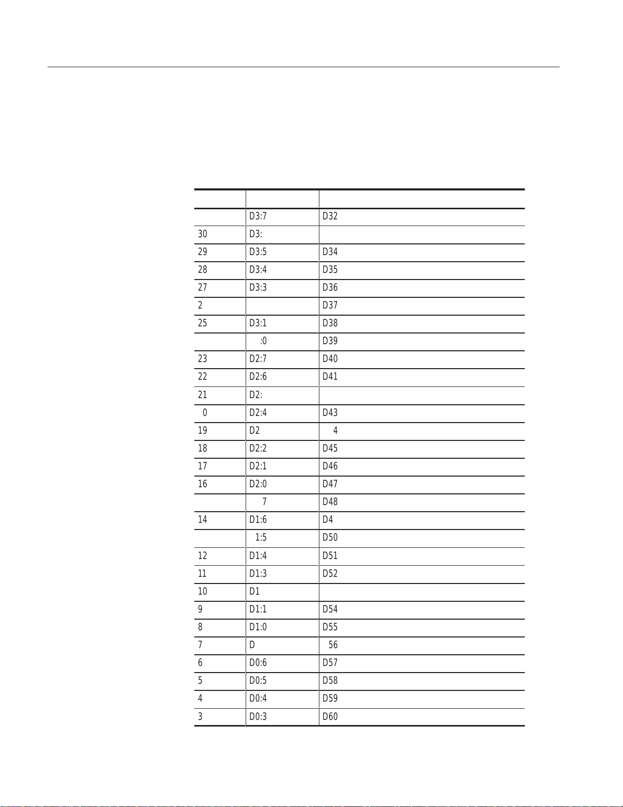
Reference: Tables
Á
Á
Á
Á
Á
Á
Á
Á
Á
Á
Table 5–7 lists the probe section and channel assignments for the Low_Data
group and the microprocessor signal to which each channel connects. By default,
the Low_Data channel group assignments are displayed in hexadecimal.
T able 5–7: Low_Data channel group assignments for 8260ITR_60X
Bit order LA channel
31
30
29
28
27
26
25
24
23
22
21
20
19
18
17
D3:7
D3:6
D3:5
D3:4
D3:3
ÁÁÁÁ
D3:2
D3:1
D3:0
D2:7
D2:6
D2:5
D2:4
ÁÁÁÁ
D2:3
D2:2
D2:1
8260ITR_60X signal name
D32
D33
D34
D35
D36
ББББББББББББ
D37
D38
D39
D40
D41
D42
D43
ББББББББББББ
D44
D45
D46
5–8
16
15
14
13
12
11
10
9
8
7
6
5
4
3
D2:0
D1:7
D1:6
D1:5
ÁÁÁÁ
D1:4
D1:3
D1:2
D1:1
D1:0
D0:7
D0:6
ÁÁÁÁ
D0:5
ÁÁÁÁ
D0:4
D0:3
D47
D48
D49
D50
ББББББББББББ
D51
D52
D53
D54
D55
D56
D57
ББББББББББББ
D58
ББББББББББББ
D59
D60
TMS562A MPC8260ITR Microprocessor Support
Page 69

Reference: Tables
Á
Á
Á
Á
Á
Á
Á
Á
T able 5–7: Low_Data channel group assignments for 8260ITR_60X
Bit order
2
1
0
LA channel
D0:2
D0:1
ÁÁÁÁ
D0:0
8260ITR_60X signal name
D61
D62
ББББББББББББ
D63
(cont.)
Table 5–8 lists the probe section and channel assignments for the Control group
and the microprocessor signal to which each channel connects. The default radix
of the Control group is SYMBOLIC on the logic analyzer. The symbol table file
name is 8260ITR_60X_Ctrl on the logic analyzer.
T able 5–8: Control channel group assignments for 8260ITR_60X
Bit order LA channel
12
11
ÁÁ
10
9
CLK:3
C2:3
ÁÁÁÁ
CLK:0
C2:1
8260ITR_60X signal name
TS~
ALE
БББББББББББ
PSDVAL~
BG~
8
7
6
5
4
ÁÁ
3
2
C2:0
C2:2
C3:6
C1:6
C2:7
ÁÁÁÁ
C3:7
C0:3
AACK~
DBG~
ABB~/IRQ2~
ARTRY~
DBB~/IRQ3~
БББББББББББ
BCTL0~
TA~
1 C3:5 PSDWE~/PGPL1
0
C0:2
TEA~
TMS562A MPC8260ITR Microprocessor Support
5–9
Page 70

Reference: Tables
Á
Á
Á
Table 5–9 lists the probe section and channel assignments for the Tsize group
and the microprocessor signal to which each channel connects. The default radix
of the Control group is SYMBOLIC on the logic analyzer. The symbol table file
name is 8260ITR_60X_Tsiz on the logic analyzer.
T able 5–9: Tsize channel group assignments for 8260ITR_60X
Bit order LA channel
4
3
2
1
0
C1:7
C1:4
C1:3
C1:2
C1:1
8260ITR_60X signal name
TBST~
TSIZ0
TSIZ1
TSIZ2
TSIZ3
Table 5–10 lists the probe section and channel assignments for the TransferType
group and the microprocessor signal to which each channel connects. By default,
the TransferType channel group assignments are displayed in hexadecimal.
T able 5–10: TransferType channel group assignments for
8260ITR_60X
Bit order LA channel
4
3
C1:0
C0:7
8260ITR_60X signal name
TT0
TT1
5–10
2
1
ÁÁ
0
C0:6
C0:5
ÁÁÁÁ
C0:4
TT2
TT3
ББББББББББББ
TT4
Table 5–11 lists the probe section and channel assignments for the TC group and
the microprocessor signal to which each channel connects. By default, the TC
channel group assignments are displayed in hexadecimal.
T able 5–11: TC channel group assignments for 8260ITR_60X
Bit order LA channel
2
1
0
C0:1
C0:0
C2:6
8260ITR_60X signal name
BNKSEL0/TC0/AP1/MODCK1~
BNKSEL1/TC1/AP2/MODCK2~
BNKSEL2/TC2/AP3/MODCK3~
TMS562A MPC8260ITR Microprocessor Support
Page 71

Reference: Tables
Á
Á
Á
Á
Á
Á
Á
Table 5–12 lists the probe section and channel assignments for the Misc group
and the microprocessor signal to which each channel connects. By default, the
Misc channel group assignments are not displayed.
T able 5–12: Misc channel group assignments for 8260ITR_60X
Bit order LA channel
9
8
7
6
5
ÁÁ
4
CLK:1
C3:1
C3:3
C3:0
C2:5
ÁÁÁÁ
C2:4
8260ITR_60X signal name
CLKIN
PSDA10/PGPL0
HRESET~
SRESET~
PSDAMUX/PGPL5
БББББББББББ
L2_HIT~/IRQ4~
3 CLK:2 CS3~
2 QUAL_2 CS1~
1 QUAL_3 CS0~
0 C3:2 BR~
Table 5–13 lists the probe section and clock and qualifier channel assignments.
The clock probes are not part of any group.
T able 5–13: Clock and Qualifier channel
assignments for 8260ITR_60X
LA channel
CLK:0
CLK:1
CLK:2
CLK:3
ÁÁÁÁ
C2:0
C2:1
C2:2
C2:3
QUAL:0
QUAL:1
QUAL:2
ÁÁÁÁ
QUAL:3
TMS562A MPC8260ITR Microprocessor Support
8260ITR_60X signal name
PSDVAL~
CLKIN as clock
CS3~
TS~
ББББББББ
AACK~
BG~
DBG~
ALE
CS2~
Not connected
CS1~
ББББББББ
CS0~
5–11
Page 72

Reference: Tables
Acquisition Setup. The TMS562A support affects the logic analyzer setup menus
(and submenus) by modifying existing fields and adding micro-specific fields.
The TMS562A support adds the selection 8260ITR_60X and 8260ITR_SNG to
the Load Support Package dialog box, under the File pulldown menu. Once the
8260ITR_60X and 8260ITR_SNG supports are loaded, the Custom clocking
mode selection in the module Setup menu is also enabled.
5–12
TMS562A MPC8260ITR Microprocessor Support
Page 73

Reference: Tables
Á
Á
Á
Á
Á
Á
Á
Á
Table 5–14 lists the 8260ITR_60X signals required for clocking and
disassembly.
T able 5–14: Signals required for clocking and
disassembly for 8260ITR_60X
MPC8260ITR
signal name
A0 – A26, BADDR27 – BADDR31
ББББББББ
(Address Group)
Channel name
A0:0–7
ББББББ
A1:0–7
–
–
–
D0–D63
(High_Data & Low_Data Groups)
–
ББББББББ
–
–
–
–
–
CLKIN
TS~
ББББББББ
ALE
PSDVAL~
BG~
A2:0–7
A3:0–7
–
E0:0–7
E1:0–7
E2:0–7
ББББББ
E3:0–7
D0:0–7
D1:0–7
D2:0–7
D3:0–7
CLK:1
CLK:3
ББББББ
C2:3
CLK:0
C2:1
BR~ C3:2
DBG~
ARTRY~
AACK~
ББББББББ
TBST~
TSIZ0
TSIZ1
TSIZ2
TSIZ3
TT0
TMS562A MPC8260ITR Microprocessor Support
C2:2
C1:6
C2:0
ББББББ
C1:7
C1:4
C1:3
C1:2
C1:1
C1:0
5–13
Page 74
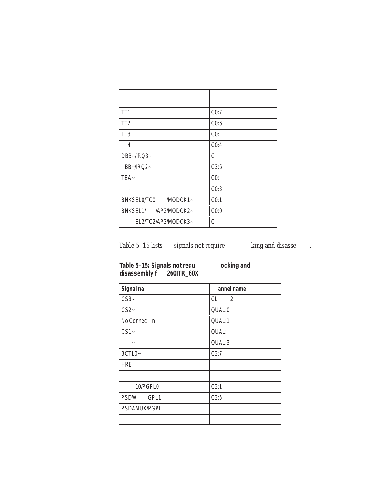
Reference: Tables
Á
Á
Á
Á
Á
Á
Á
Á
T able 5–14: Signals required for clocking and
disassembly for 8260ITR_60X (cont.)
MPC8260ITR
signal name
TT1
Channel name
C0:7
TT2
TT3
TT4
DBB~/IRQ3~
ABB~/IRQ2~
ББББББББ
TEA~
TA~
BNKSEL0/TC0/AP1/MODCK1~
BNKSEL1/TC1/AP2/MODCK2~
BNKSEL2/TC2/AP3/MODCK3~
C0:6
C0:5
C0:4
C2:7
C3:6
ББББББ
C0:2
C0:3
C0:1
C0:0
C2:6
Table 5–15 lists the signals not required for clocking and disassembly.
T able 5–15: Signals not required for clocking and
disassembly for 8260ITR_60X
Signal name Channel name
CS3~ CLOCK:2
5–14
CS2~
ББББББББ
No Connection
ББББББББ
CS1~
CS0~
BCTL0~
HRESET~
SRESET~
PSDA10/PGPL0
PSDWE~/PGPL1
ББББББББ
PSDAMUX/PGPL5
L2_HIT~/IRQ4~
QUAL:0
БББББББ
QUAL:1
БББББББ
QUAL:2
QUAL:3
C3:7
C3:3
C3:0
C3:1
C3:5
БББББББ
C2:5
C2:4
TMS562A MPC8260ITR Microprocessor Support
Page 75

Reference: Tables
Á
Á
Á
Á
Á
Á
Á
Á
8260ITR_SNG Channel
Group Assignments
Table 5–16 lists the probe section and channel assignments for the Address
group and the microprocessor signal to which each channel connects. By default,
the Address channel group assignments are displayed in hexadecimal.
T able 5–16: Address channel group assignments for
8260ITR_SNG
8260ITR_SNG signal
Bit order LA channel
31
30
29
28
27
26
25
24
23
22
A3:7
ББББББ
A3:6
A3:5
A3:4
A3:3
A3:2
A3:1
A3:0
ББББББ
A2:7
A2:6
name
A0
БББББББ
A1
A2
A3
A4
A5
A6
A7
БББББББ
A8
A9
21
20
19
18
17
16
15
14
13
12
11
10
9
8
7
6
5
A2:5
A2:4
A2:3
A2:2
A2:1
ББББББ
A2:0
A1:7
A1:6
A1:5
A1:4
A1:3
A1:2
ББББББ
A1:1
A1:0
A0:7
A0:6
A0:5
A10
A11
A12
A13
A14
БББББББ
A15
A16
A17
A18
A19
A20
A21
БББББББ
A22
A23
A24
A25
A26
4
A0:4
TMS562A MPC8260ITR Microprocessor Support
A27
5–15
Page 76

Reference: Tables
T able 5–16: Address channel group assignments for
8260ITR_SNG (cont.)
8260ITR_SNG signal
Bit order
3
LA channel
A0:3
name
A28
2
1
0
A0:2
A0:1
A0:0
A29
A30
A31
TraceAddr Group Assignments. The TraceAddr group is used for tracking the
program flow when the cache is enabled. The default radix for this group is OFF.
The TraceAddr group is a synthesized group. The TraceAddr group uses the
“Trace Write Address” values in the disassembly option to trace the writes to
noncacheable regions that are used for reading Memory Image.
1. Enter the “Trace Write Address” value in the disassembly option field.
2. Enable the Branch Trace Exception by setting the BE field in the MSR of the
MPC8260 support. When the Branch Trace Exception subroutine is
encountered, the SRR0 register contains the target address of the branch that
was just executed.
3. In the Trace Exception subroutine, you need to write the value stored in the
SRR0 register into the noncacheable region of the “Trace Write Address”
field. The SRR0 value needs to be a 32 bit write since the address is 32 bits.
Once you have entered the SRR0 value, the TraceAddr field then contains
the value of the written data that points to the target of the branch instruction. When reading from the Memory Image starts, the TraceAddr field then
contains the address to be traced from the Memory Image.
5–16
Table 5–17 lists the probe section and channel assignments for the High_Data
group and the microprocessor signal to which each channel connects. By default,
the High_Data channel group assignments are displayed in hexadecimal.
NOTE. The Trace Write Address must be word aligned.
T able 5–17: High_Data channel group assignments for
8260ITR_SNG
Bit order LA channel
31
30
E3:7
E3:6
8260ITR_SNG signal name
D0
D1
TMS562A MPC8260ITR Microprocessor Support
Page 77

T able 5–17: High_Data channel group assignments for
Á
Á
Á
Á
Á
Á
Á
Á
Á
Á
Á
Á
8260ITR_SNG
(cont.)
Reference: Tables
Bit order
29
28
27
26
ÁÁ
25
24
23
22
21
20
19
ÁÁ
18
17
16
15
14
LA channel
E3:5
E3:4
E3:3
E3:2
ÁÁÁÁ
E3:1
E3:0
E2:7
E2:6
E2:5
E2:4
E2:3
ÁÁÁÁ
E2:2
E2:1
E2:0
E1:7
E1:6
8260ITR_SNG signal name
D2
D3
D4
D5
БББББББББ
D6
D7
D8
D9
D10
D11
D12
БББББББББ
D13
D14
D15
D16
D17
13
12
ÁÁ
11
10
9
8
7
6
5
ÁÁ
4
3
2
1
0
E1:5
E1:4
ÁÁÁÁ
E1:3
E1:2
E1:1
E1:0
E0:7
E0:6
E0:5
ÁÁÁÁ
E0:4
E0:3
E0:2
E0:1
E0:0
D18
D19
БББББББББ
D20
D21
D22
D23
D24
D25
D26
БББББББББ
D27
D28
D29
D30
D31
TMS562A MPC8260ITR Microprocessor Support
5–17
Page 78

Reference: Tables
Á
Á
Á
Á
Á
Á
Á
Á
Á
Á
Á
Á
Table 5–18 lists the probe section and channel assignments for the Low_Data
group and the microprocessor signal to which each channel connects. By default,
the Low_Data channel group assignments are displayed in hexadecimal.
T able 5–18: Low_Data channel group assignments for
8260ITR_SNG
Bit order LA channel
31
ÁÁ
30
29
28
27
26
25
24
ÁÁ
23
22
21
20
19
18
17
ÁÁ
16
D3:7
ÁÁÁÁ
D3:6
D3:5
D3:4
D3:3
D3:2
D3:1
D3:0
ÁÁÁÁ
D2:7
D2:6
D2:5
D2:4
D2:3
D2:2
D2:1
ÁÁÁÁ
D2:0
8260ITR_SNG signal name
D32
БББББББББ
D33
D34
D35
D36
D37
D38
D39
БББББББББ
D40
D41
D42
D43
D44
D45
D46
БББББББББ
D47
5–18
15
14
13
12
11
10
ÁÁ
9
8
7
6
5
4
D1:7
D1:6
D1:5
D1:4
D1:3
D1:2
ÁÁÁÁ
D1:1
D1:0
D0:7
D0:6
D0:5
D0:4
D48
D49
D50
D51
D52
D53
БББББББББ
D54
D55
D56
D57
D58
D59
TMS562A MPC8260ITR Microprocessor Support
Page 79

T able 5–18: Low_Data channel group assignments for
Á
Á
Á
Á
Á
Á
8260ITR_SNG
(cont.)
Reference: Tables
Bit order
3
2
1
0
ÁÁ
LA channel
D0:3
D0:2
D0:1
D0:0
ÁÁÁÁ
8260ITR_SNG signal name
D60
D61
D62
D63
БББББББББ
Table 5–19 lists the probe section and channel assignments for the Control group
and the microprocessor signal to which each channel connects. The default radix
of the Control group is SYMBOLIC on the logic analyzer. The symbol table file
name is 8260ITR_SNG_Ctrl on the logic analyzer.
T able 5–19: Control channel group assignments for
8260ITR_SNG
Bit order LA channel
4
3
2
ÁÁ
1
CLK:0
C2:1
C2:2
ÁÁÁÁ
C3:7
8260ITR_SNG signal name
PSDVAL~
POE~/PSDRAS~/PGPL2
PSDCAS~/PGPL3
БББББББББ
BCTL0~
0
C3:5
PSDWE~/PGPL1
NOTE. The signals POE~/PSDRAS~/PGPL2 and PSDCAS~/PGPL3 are used as
PSDCAS~ and PSDCAS~ respectively in 8260ITR_SNG.
PortWidth Group Assignments. This group displays the PortWidth (in number of
bytes) corresponding to the current sample. In Memory Image mode this displays
the PortWidth only for the samples belonging to fetch stream and not for the
ones read from the memory image.
TMS562A MPC8260ITR Microprocessor Support
5–19
Page 80

Reference: Tables
Á
Á
Á
Á
Á
Á
Á
Á
Á
Á
Á
Á
Table 5–20 lists the probe section and channel assignments for the Misc group
and the microprocessor signal to which each channel connects. By default, the
Misc channel group assignments are not displayed.
T able 5–20: Misc channel group assignments for
8260ITR_SNG
Bit order LA channel
30
29
28
27
26
25
24
ÁÁ
23
22
21
20
19
18
17
ÁÁ
16
15
Clock:1
C3:1
C3:3
C3:0
C2:5
C2:4
Clock:2
ÁÁÁÁ
Qual_2
Qual_1
C3:2
C0:1
C0:0
C2:6
C1:0
ÁÁÁÁ
C0:7
C0:6
8260ITR_SNG signal name
CLKIN
PSDA10/PGPL0
HRESET~
SRESET~
PSDAMUX/PGPL5
L2_HIT~/IRQ4~
CS3~
БББББББББ
CS1~
CS0~
BR~
BNKSEL0/TC0/AP1/MODCK1~
BNKSEL1/TC1/AP2/MODCK2~
BNKSEL2/TC2/AP3/MODCK3~
TT0
БББББББББ
TT1
TT2
5–20
14
13
12
11
10
ÁÁ
9
8
7
6
5
4
3
ÁÁ
C0:5
C0:4
C1:7
C1:4
C1:3
ÁÁÁÁ
C1:2
C1:1
Clock:3
C2:3
C2:0
C3:6
C1:6
ÁÁÁÁ
TT3
TT4
TBST~
TSIZ0
TSIZ1
БББББББББ
TSIZ2
TSIZ3
TS~
ALE
AACK~
ABB~/IRQ2~
ARTRY~
БББББББББ
TMS562A MPC8260ITR Microprocessor Support
Page 81

T able 5–20: Misc channel group assignments for
Á
Á
Á
Á
8260ITR_SNG (cont.)
Reference: Tables
Bit order
2
1
0
LA channel
C2:7
C0:3
C0:2
8260ITR_SNG signal name
DBB~/IRQ3~
TA~
TEA~
Table 5–21 lists the probe section and clock and qualifier channel assignments.
The clock probes are not part of any group.
T able 5–21: Clock and Qualifier channel
assignments for 8260ITR_SNG
8260ITR_SNG
signal name
CLK:0
CLK:1
CLK:2
CLK:3
ÁÁÁÁ
C2:0
C2:1
Channel name
PSDVAL~
CLKIN as clock
CS3~
TS~
ББББББ
AACK~
POE~/PSDRAS~/PGPL2
C2:2
C2:3
QUAL:0
QUAL:1
QUAL:2
ÁÁÁÁ
QUAL:3
PSDCAS~/PGPL3
ALE
CS2~
Not connected
CS1~
ББББББ
CS0~
TMS562A MPC8260ITR Microprocessor Support
5–21
Page 82

Reference: Tables
Á
Á
Á
Á
Table 5–22 Signals required for clocking and disassembly for the 8260ITR_SNG
interface.
T able 5–22: Signals required for clocking and disassembly for
8260ITR_SNG
8260ITR_SNG signal name Channel name
A0 – A31
A0:0–7
(Address Group)
–
–
–
D0–D63
ББББББББ
(High_Data & Low_Data Groups)
–
–
–
–
–
–
ББББББББ
CLKIN
PSDVAL~
POE~/PSDRAS~/PGPL2
PSDCAS~/PGPL3
BCTL0~
A1:0–7
A2:0–7
A3:0–7
–
E0:0–7
БББББББББ
E1:0–7
E2:0–7
E3:0–7
D0:0–7
D1:0–7
D2:0–7
D3:0–7
БББББББББ
CLK:1
CLK:0
C2:1
C2:2
C3:7
5–22
PSDWE~/PGPL1
C3:5
Table 5–23 Signals not required for clocking and disassembly for the
8260ITR_SNG interface.
T able 5–23: Signals not required for clocking and disassembly for
8260ITR_SNG
8260ITR_SNG
signal name
PSDA10/PGPL0
HRESET~
SRESET~
Channel name
C3:1
C3:3
C3:0
TMS562A MPC8260ITR Microprocessor Support
Page 83

T able 5–23: Signals not required for clocking and disassembly for
Á
Á
Á
Á
Á
Á
Á
Á
8260ITR_SNG (cont.)
8260ITR_SNG
signal name
PSDAMUX/PGPL5
Channel name
C2:5
Reference: Tables
L2_HIT~/IRQ4~
CS3~
CS1~
CS0~
BR~
БББББББББ
BNKSEL0/TC0/AP1/MODCK1~
BNKSEL1/TC1/AP2/MODCK2~
BNKSEL2/TC2/AP3/MODCK3~
TT0
TT1
TT2
TT3
БББББББББ
TT4
TBST~
TSIZ0
TSIZ1
TSIZ2
C2:4
Clock:2
Qual_2
Qual_1
C3:2
ББББББББ
C0:1
C0:0
C2:6
C1:0
C0:7
C0:6
C0:5
ББББББББ
C0:4
C1:7
C1:4
C1:3
C1:2
TSIZ3
TS~
БББББББББ
ALE
AACK~
ABB~/IRQ2~
ARTRY~
DBB~/IRQ3~
TA~
TEA~
БББББББББ
TMS562A MPC8260ITR Microprocessor Support
C1:1
Clock:3
ББББББББ
C2:3
C2:0
C3:6
C1:6
C2:7
C0:3
C0:2
ББББББББ
5–23
Page 84

Reference: Tables
CPU To Mictor Connections
For design purposes, you may need to make connections between the CPU and
the Mictor pins of the P6434 Mass Termination Probe. Refer to the P6434 Mass
Termination Probe manual, Tektronix part number 070-9793-XX, for more
information on mechanical specifications.
CAUTION. To protect the CPU and the inputs of the module, it is recommended
that a 180 W resistor is connected in series between each ball pad of the CPU
and each pin of the Mictor connector. The resistor must be within 1/2 inch of the
ball pad of the CPU.
The recommended pin assignment is the Amp pin assignment, because the AMP
circuit board layout model and other commercial CAD packages use the Amp
numbering scheme. In order to use the Tektronix numbering scheme a custom
model must be created for your circuit board layout CAD application. See
Figure 5–24.
Table 5–24: Recommended pin assignments for a Mictor connector (component
side)
Type of pin assignment
Recommended
Comments
Recommended. This pin assignment is the industry
standard and is what we recommend that you use.
Pin 1
Pin 37
Amp Pin Assignment
Not Recommended
Pin 2
Pin 38
Not recommended. This pin assignment was
previously used by Tektronix but is no longer
Pin 1
Pin 2
Non Standard Pin Assignment
Pin 38
Pin 37
recommended due to incompatibility with other
commercial CAD packages.
5–24
TMS562A MPC8260ITR Microprocessor Support
Page 85

Reference: Tables
Á
Á
Á
БББББ
Á
Á
Á
БББББ
БББББ
БББББ
БББББ
БББББ
БББББ
Á
Á
Á
БББББ
Á
Á
Á
БББББ
БББББ
БББББ
БББББ
БББББ
БББББ
Á
Á
Á
БББББ
Á
Á
Á
БББББ
БББББ
БББББ
БББББ
БББББ
БББББ
Á
Á
Á
БББББ
Á
Á
Á
БББББ
БББББ
БББББ
БББББ
8260ITR_60X Mictor
Connections
Tables 5–25 through 5–27 list the microprocessor signals visible at the mictor
connectors.
T able 5–25: CPU to Mictor connections for Mictor A pins for 8260ITR_60X
AMP
Mictor A
pin number
(recommended)
Tektronix
Mictor A
pin number
1 1 GND GND GND
3 2 GND GND GND
5
ÁÁÁ
7
9
11
13
15
17
19
ÁÁÁ
21
3
ÁÁÁÁ
4
5
6
7
8
9
10
ÁÁÁÁ
11
Logic
analyzer
channel
CLK:0
ÁÁ
A3:7
A3:6
A3:5
A3:4
A3:3
A3:2
A3:1
ÁÁ
A3:0
8260ITR_60X
signal name
PSDVAL~
ÁÁÁ
A0
A1
A2
A3
A4
A5
A6
ÁÁÁ
A7
Comments
Data signal
ББББББ
Address
Address
Address
Address
Address
Address
Address
ББББББ
Address
23
25
27
29
31
33
ÁÁÁ
35
37
38
36
34
32
30
ÁÁÁ
28
26
24
22
12
13
14
15
16
17
ÁÁÁÁ
18
19
20
21
22
23
24
ÁÁÁÁ
25
26
27
28
A2:7
A2:6
A2:5
A2:4
A2:3
A2:2
ÁÁ
A2:1
A2:0
A0:0
A0:1
A0:2
A0:3
A0:4
ÁÁ
A0:5
A0:6
A0:7
A1:0
A8
A9
A10
A11
A12
A13
ÁÁÁ
A14
A15
BADDR31
BADDR30
BADDR29
BADDR28
BADDR27
ÁÁÁ
A26
A25
A24
A23
Address
Address
Address
Address
Address
Address
ББББББ
Address
Address
Address
Address
Address
Address
Address
ББББББ
Address
Address
Address
Address
TMS562A MPC8260ITR Microprocessor Support
5–25
Page 86

Reference: Tables
Á
Á
Á
Á
Á
Á
Á
Á
Á
Á
Á
Á
Á
Á
Á
Á
Á
Á
Á
Á
Á
Á
Á
Á
Á
T able 5–25: CPU to Mictor connections for Mictor A pins for 8260ITR_60X (cont.)
AMP
Mictor A
pin number
(recommended)
20
18
ÁÁÁ
16
14
12
10
8
6
Tektronix
Mictor A
pin number
29
30
ÁÁÁÁ
31
32
33
34
35
36
Logic
analyzer
channel
A1:1
A1:2
ÁÁ
A1:3
A1:4
A1:5
A1:6
A1:7
CLK:1
8260ITR_60X
signal name
A22
A21
ÁÁÁ
A20
A19
A18
A17
A16
CLKIN
Comments
Address
Address
ББББББ
Address
Address
Address
Address
Address
Clock
T able 5–26: CPU to Mictor connections for Mictor C pins for 8260ITR_60X
AMP
Mictor C
pin number
(recommended)
01
Tektronix
Mictor C
pin number
01
Logic
analyzer
channel
–
8260ITR_60X
signal name
–
Comments
Not Connected
03
05
07
09
11
ÁÁÁ
13
15
17
ÁÁÁ
19
21
23
25
ÁÁÁ
27
ÁÁÁ
02
03
04
05
06
ÁÁÁ
07
08
09
ÁÁÁ
10
11
12
13
ÁÁÁ
14
ÁÁÁ
–
CLK:3
C3:7
C3:6
C3:5
ÁÁ
C3:4
C3:3
C3:2
ÁÁ
C3:1
C3:0
C2:7
C2:6
ÁÁ
C2:5
ÁÁ
–
TS~
BCTL0~
ABB~/IRQ2~
PSDWE~/PGPL
ÁÁÁÁ
1
–
HRESET~
BR~
ÁÁÁÁ
PSDA10/PGPL0
SRESET~
DBB~/IRQ3~
BNKSEL2/TC2/
ÁÁÁÁ
AP3/MODCK3~
PSDAMUX/
PGPL5
ÁÁÁÁ
Not Connected
Transfer Start
Buffer Control 0
Address Bus Busy
60x BUS SDRAM write en-
ББББББ
able
–
Hard Reset
Bus Request
ББББББ
Soft Reset
Data Bus Busy
Transfer Code 2
ББББББ
60x bus SDRAM Address
Multiplexer
ББББББ
5–26
TMS562A MPC8260ITR Microprocessor Support
Page 87

Reference: Tables
Á
Á
Á
Á
Á
Á
Á
Á
Á
Á
Á
Á
Á
Á
Á
Á
Á
Á
Á
Á
Á
Á
Á
Á
Á
T able 5–26: CPU to Mictor connections for Mictor C pins for 8260ITR_60X (cont.)
AMP
Mictor C
pin number
(recommended)
29
Tektronix
Mictor C
pin number
15
Logic
analyzer
channel
C2:4
8260ITR_60X
signal name
L2_HIT~/IRQ4~
Comments
L2 Cache Signal
31
ÁÁÁ
33
35
37
38
ÁÁÁ
36
ÁÁÁ
34
32
30
28
26
ÁÁÁ
24
22
20
18
16
16
ÁÁÁ
17
18
19
20
ÁÁÁ
21
ÁÁÁ
22
23
24
25
26
ÁÁÁ
27
28
29
30
31
C2:3
ÁÁ
C2:2
C2:1
C2:0
C0:0
ÁÁ
C0:1
ÁÁ
C0:2
C0:3
C0:4
C0:5
C0:6
ÁÁ
C0:7
C1:0
C1:1
C1:2
C1:3
ALE
ÁÁÁÁ
DBG~
BG~
AACK~
BNKSEL1/TC1/
ÁÁÁÁ
AP2/MODCK2~
BNKSEL0/TC0/
AP1/MODCK1~
ÁÁÁÁ
TEA~
TA~
TT4
TT3
TT2
ÁÁÁÁ
TT1
TT0
TSIZ3
TSIZ2
TSIZ1
Address Latch Enable
ББББББ
Data Bus Grant
Bus Grant
Address Acknowledge
Transfer Code 1
ББББББ
Transfer Code 0
ББББББ
Transfer Error Acknowledge
Transfer Acknowledge
Transfer T ype
Transfer T ype
Transfer T ype
ББББББ
Transfer T ype
Transfer T ype
Transfer Size
Transfer Size
Transfer Size
14
12
ÁÁÁ
10
08
06
04
02
TMS562A MPC8260ITR Microprocessor Support
32
33
ÁÁÁ
34
35
36
37
38
C1:4
C1:5
ÁÁ
C1:6
C1:7
QUAL_1
–
–
TSIZ0
–
ÁÁÁÁ
ARTRY~
TBST~
Not connected
–
–
Transfer Size
–
ББББББ
Address Retry
Transfer Burst
–
–
–
5–27
Page 88

Reference: Tables
Á
Á
Á
Á
Á
Á
Á
Á
Á
Á
Á
Á
Á
Á
Á
Á
Á
Á
Á
Á
Á
Á
Á
Á
Á
T able 5–27: CPU to Mictor connections for Mictor E pins for 8260ITR_60X
AMP
Mictor E
pin number
(recommended)
1
Tektronix
Mictor E
pin number
1
Logic
analyzer
channel
–
8260ITR_60X
signal name
–
Comments
Not Connected
3
ÁÁÁ
5
7
9
11
13
15
17
ÁÁÁ
19
21
23
25
27
29
31
ÁÁÁ
33
35
2
ÁÁÁ
3
4
5
6
7
8
9
ÁÁÁ
10
11
12
13
14
15
16
ÁÁÁ
17
18
–
ÁÁ
Qual_3
E3:7
E3:6
E3:5
E3:4
E3:3
E3:2
ÁÁ
E3:1
E3:0
E2:7
E2:6
E2:5
E2:4
E2:3
ÁÁ
E2:2
E2:1
–
БББББ
CS0~
D0
D1
D2
D3
D4
D5
БББББ
D6
D7
D8
D9
D10
D11
D12
БББББ
D13
D14
Not Connected
БББББ
–
High_Data
High_Data
High_Data
High_Data
High_Data
High_Data
БББББ
High_Data
High_Data
High_Data
High_Data
High_Data
High_Data
High_Data
БББББ
High_Data
High_Data
5–28
37
38
36
34
32
ÁÁÁ
30
28
26
24
22
20
18
ÁÁÁ
19
20
21
22
23
ÁÁÁ
24
25
26
27
28
29
30
ÁÁÁ
E2:0
E0:0
E0:1
E0:2
E0:3
ÁÁ
E0:4
E0:5
E0:6
E0:7
E1:0
E1:1
E1:2
ÁÁ
D15
D31
D30
D29
D28
БББББ
D27
D26
D25
D24
D23
D22
D21
БББББ
High_Data
High_Data
High_Data
High_Data
High_Data
БББББ
High_Data
High_Data
High_Data
High_Data
High_Data
High_Data
High_Data
БББББ
TMS562A MPC8260ITR Microprocessor Support
Page 89

Reference: Tables
Á
Á
Á
Á
Á
Á
Á
Á
Á
Á
Á
Á
Á
Á
Á
T able 5–27: CPU to Mictor connections for Mictor E pins for 8260ITR_60X (cont.)
AMP
Mictor E
pin number
(recommended)
16
Tektronix
Mictor E
pin number
31
Logic
analyzer
channel
E1:3
8260ITR_60X
signal name
D20
Comments
High_Data
14
ÁÁÁ
12
10
8
6
4
2
32
ÁÁÁ
33
34
35
36
37
38
E1:4
ÁÁ
E1:5
E1:6
E1:7
Qual_2
–
–
D19
БББББ
D18
D17
D16
CS1~
–
–
High_Data
БББББ
High_Data
High_Data
High_Data
–
–
–
T able 5–28: CPU to Mictor connections for Mictor D pins for 8260ITR_60X
AMP
Mictor D
pin number
(recommended)
1
3
5
7
Tektronix
Mictor D
pin number
1
2
3
4
Logic
analyzer
channel
–
–
–
D3:7
8260ITR_60X
signal name
–
–
–
D32
Comments
Not Connected
Not Connected
Not Connected
Low_Data
9
11
13
ÁÁÁ
15
17
19
21
23
25
27
ÁÁÁ
29
31
TMS562A MPC8260ITR Microprocessor Support
5
6
7
ÁÁÁ
8
9
10
11
12
13
14
ÁÁÁ
15
16
D3:6
D3:5
D3:4
ÁÁ
D3:3
D3:2
D3:1
D3:0
D2:7
D2:6
D2:5
ÁÁ
D2:4
D2:3
D33
D34
D35
БББББ
D36
D37
D38
D39
D40
D41
D42
БББББ
D43
D44
Low_Data
Low_Data
Low_Data
БББББ
Low_Data
Low_Data
Low_Data
Low_Data
Low_Data
Low_Data
Low_Data
БББББ
Low_Data
Low_Data
5–29
Page 90

Reference: Tables
Á
Á
Á
Á
Á
Á
Á
Á
Á
Á
Á
Á
Á
Á
Á
T able 5–28: CPU to Mictor connections for Mictor D pins for 8260ITR_60X (cont.)
AMP
Mictor D
pin number
(recommended)
33
Tektronix
Mictor D
pin number
17
Logic
analyzer
channel
D2:2
8260ITR_60X
signal name
D45
Comments
Low_Data
35
ÁÁÁ
37
38
36
34
32
30
28
ÁÁÁ
26
24
22
20
18
16
14
ÁÁÁ
12
10
18
ÁÁÁ
19
20
21
22
23
24
25
ÁÁÁ
26
27
28
29
30
31
32
ÁÁÁ
33
34
D2:1
ÁÁ
D2:0
D0:0
D0:1
D0:2
D0:3
D0:4
D0:5
ÁÁ
D0:6
D0:7
D1:0
D1:1
D1:2
D1:3
D1:4
ÁÁ
D1:5
D1:6
D46
БББББ
D47
D63
D62
D61
D60
D59
D58
БББББ
D57
D56
D55
D54
D53
D52
D51
БББББ
D50
D49
Low_Data
БББББ
Low_Data
Low_Data
Low_Data
Low_Data
Low_Data
Low_Data
Low_Data
БББББ
Low_Data
Low_Data
Low_Data
Low_Data
Low_Data
Low_Data
Low_Data
БББББ
Low_Data
Low_Data
5–30
8
6
4
2
35
36
37
38
D1:7
–
–
–
D48
–
–
–
Low_Data
–
–
–
TMS562A MPC8260ITR Microprocessor Support
Page 91

Reference: Tables
Á
Á
Á
Á
Á
Á
Á
Á
Á
Á
Á
Á
Á
Á
Á
Á
Á
Á
Á
Á
8260ITR_SNG Mictor
Connections
Tables 5–29 and 5–31 list the microprocessor signals visible at the mictor
connectors.
T able 5–29: CPU to Mictor connections for Mictor A pins for 8260ITR_SNG
AMP
Mictor A
pin number
(recommended)
1
3
5
ÁÁÁ
7
9
11
13
15
17
19
ÁÁÁ
21
Tektronix
Mictor A
pin number
1
2
3
ÁÁÁ
4
5
6
7
8
9
10
ÁÁÁ
11
Logic
analyzer
channel
–
–
CLK:0
ÁÁ
A3:7
A3:6
A3:5
A3:4
A3:3
A3:2
A3:1
ÁÁ
A3:0
8260ITR_SNG
signal name
–
–
PSDVAL~
БББББ
A0
A1
A2
A3
A4
A5
A6
БББББ
A7
Comments
Not Connected
Not Connected
Data signal
БББББ
Address
Address
Address
Address
Address
Address
Address
БББББ
Address
23
25
27
29
31
33
ÁÁÁ
35
37
38
36
34
32
30
ÁÁÁ
28
26
24
22
12
13
14
15
16
17
ÁÁÁ
18
19
20
21
22
23
24
ÁÁÁ
25
26
27
28
A2:7
A2:6
A2:5
A2:4
A2:3
A2:2
ÁÁ
A2:1
A2:0
A0:0
A0:1
A0:2
A0:3
A0:4
ÁÁ
A0:5
A0:6
A0:7
A1:0
A8
A9
A10
A11
A12
A13
БББББ
A14
A15
A31
A30
A29
A28
A27
БББББ
A26
A25
A24
A23
Address
Address
Address
Address
Address
Address
БББББ
Address
Address
Address
Address
Address
Address
Address
БББББ
Address
Address
Address
Address
TMS562A MPC8260ITR Microprocessor Support
5–31
Page 92

Reference: Tables
Á
Á
Á
Á
Á
Á
Á
Á
Á
Á
Á
Á
Á
Á
Á
Á
Á
Á
Á
Á
Á
Á
Á
Á
Á
T able 5–29: CPU to Mictor connections for Mictor A pins for 8260ITR_SNG (cont.)
AMP
Mictor A
pin number
(recommended)
20
Tektronix
Mictor A
pin number
29
Logic
analyzer
channel
A1:1
8260ITR_SNG
signal name
A22
Comments
Address
18
ÁÁÁ
16
14
12
10
8
6
30
ÁÁÁ
31
32
33
34
35
36
A1:2
ÁÁ
A1:3
A1:4
A1:5
A1:6
A1:7
CLK:1
A21
БББББ
A20
A19
A18
A17
A16
CLKIN
Address
БББББ
Address
Address
Address
Address
Address
Clock
T able 5–30: CPU to Mictor connections for Mictor C pins for 8260ITR_SNG
AMP
Mictor C
pin number
(recommended)
1
3
5
7
Tektronix
Mictor C
pin number
1
2
3
4
Logic
analyzer
channel
–
–
CLK:3
C3:7
8260ITR_SNG
signal name
–
–
TS~
BCTL0~
Comments
Not Connected
Not Connected
Transfer Start
Buffer Control 0
5–32
9
11
ÁÁÁ
13
15
17
ÁÁÁ
19
21
23
25
ÁÁÁ
27
ÁÁÁ
5
6
ÁÁÁ
7
8
9
ÁÁÁ
10
11
12
13
ÁÁÁ
14
ÁÁÁ
C3:6
C3:5
ÁÁ
C3:4
C3:3
C3:2
ÁÁ
C3:1
C3:0
C2:7
C2:6
ÁÁ
C2:5
ÁÁ
ABB~/IRQ2~
PSDWE~/PGPL1
ÁÁÁÁ
–
HRESET~
BR~
ÁÁÁÁ
PSDA10/PGPL0
SRESET~
DBB~/IRQ3~
BNKSEL2/TC2/A
ÁÁÁÁ
P3/MODCK3~
PSDAMUX/
PGPL5
ÁÁÁÁ
Address Bus Busy
60x Bus SDRAM Write En-
ББББББ
able
–
Hard Reset
Bus Request
ББББББ
60x bus SDRAM A10
Soft Reset
Data Bus Busy
Transfer Code 2
ББББББ
60x bus SDRAM Address
Multiplexer
ББББББ
TMS562A MPC8260ITR Microprocessor Support
Page 93

Reference: Tables
Á
Á
Á
Á
Á
Á
Á
Á
Á
Á
Á
Á
Á
Á
Á
Á
Á
Á
Á
Á
Á
Á
Á
Á
Á
Á
Á
Á
Á
Á
T able 5–30: CPU to Mictor connections for Mictor C pins for 8260ITR_SNG (cont.)
AMP
Mictor C
pin number
(recommended)
29
31
ÁÁÁ
33
35
ÁÁÁ
37
38
ÁÁÁ
36
ÁÁÁ
34
32
30
28
26
Tektronix
Mictor C
pin number
15
16
ÁÁÁ
17
18
ÁÁÁ
19
20
ÁÁÁ
21
ÁÁÁ
22
23
24
25
26
Logic
analyzer
channel
C2:4
C2:3
ÁÁ
C2:2
C2:1
ÁÁ
C2:0
C0:0
ÁÁ
C0:1
ÁÁ
C0:2
C0:3
C0:4
C0:5
C0:6
8260ITR_SNG
signal name
L2_HIT~/IRQ4~
ALE
ÁÁÁÁ
PSDCAS~/PGPL3
POE~/PSDRAS~/
PGPL2
ÁÁÁÁ
AACK~
BNKSEL1/TC1/A
P2/MODCK2~
ÁÁÁÁ
BNKSEL0/TC0/A
P1/MODCK1~
ÁÁÁÁ
TEA~
TA~
TT4
TT3
TT2
Comments
L2 Cache Signal
Address Latch enable
ББББББ
60x BUS SDRAM CAS
60X Bus SDRAM RAS
ББББББ
Address Acknowledge
Transfer code 1
ББББББ
Transfer Code 0
ББББББ
Transfer Error Acknowledge
Transfer Acknowledge
Transfer T ype
Transfer T ype
Transfer T ype
24
22
ÁÁÁ
20
18
16
14
12
10
8
ÁÁÁ
6
4
2
27
28
ÁÁÁ
29
30
31
32
33
34
35
ÁÁÁ
36
37
38
C0:7
C1:0
ÁÁ
C1:1
C1:2
C1:3
C1:4
C1:5
C1:6
C1:7
ÁÁ
Qual_1
–
–
TT1
TT0
ÁÁÁÁ
TSIZ3
TSIZ2
TSIZ1
TSIZ0
ARTRY~
TBST~
ÁÁÁÁ
Not connected
–
–
Transfer T ype
Transfer T ype
ББББББ
Transfer Size
Transfer Size
Transfer Size
Transfer Size
Address Retry
Transfer Burst
ББББББ
–
–
–
TMS562A MPC8260ITR Microprocessor Support
5–33
Page 94

Reference: Tables
ББББББ
Á
Á
Á
ББББББ
Á
Á
ББББББ
ББББББ
ББББББ
ББББББ
ББББББ
ББББББ
Á
Á
Á
ББББББ
Á
Á
ББББББ
ББББББ
ББББББ
ББББББ
ББББББ
ББББББ
Á
Á
Á
ББББББ
Á
Á
ББББББ
ББББББ
ББББББ
ББББББ
ББББББ
ББББББ
Á
Á
Á
ББББББ
Á
Á
ББББББ
ББББББ
ББББББ
ББББББ
ББББББ
ББББББ
Á
Á
Á
ББББББ
Á
Á
T able 5–31: CPU to Mictor connections for Mictor E pins for 8260ITR_SNG
AMP
Mictor E
pin number
(recommended)
1
Tektronix
Mictor E
pin number
1
Logic
analyzer
channel
–
8260ITR_SNG
signal name
–
Comments
Not Connected
3
ÁÁÁ
5
7
9
11
13
15
17
ÁÁÁ
19
21
23
25
27
29
31
ÁÁÁ
33
35
2
ÁÁÁ
3
4
5
6
7
8
9
ÁÁÁ
10
11
12
13
14
15
16
ÁÁÁ
17
18
Qual_3
ÁÁÁ
–
E3:7
E3:6
E3:5
E3:4
E3:3
E3:2
ÁÁÁ
E3:1
E3:0
E2:7
E2:6
E2:5
E2:4
E2:3
ÁÁÁ
E2:2
E2:1
CS0~
БББББ
–
D0
D1
D2
D3
D4
D5
БББББ
D6
D7
D8
D9
D10
D11
D12
БББББ
D13
D14
Not Connected
ÁÁÁÁ
SystemReset
High_Data
High_Data
High_Data
High_Data
High_Data
High_Data
ÁÁÁÁ
High_Data
High_Data
High_Data
High_Data
High_Data
High_Data
High_Data
ÁÁÁÁ
High_Data
High_Data
5–34
37
38
36
34
32
ÁÁÁ
30
28
26
24
22
20
18
ÁÁÁ
19
20
21
22
23t
ÁÁÁ
24
25
26
27
28
29
30
ÁÁÁ
E2:0
E0:0
E0:1
E0:2
E0:3
ÁÁÁ
E0:4
E0:5
E0:6
E0:7
E1:0
E1:1
E1:2
ÁÁÁ
D15
D31
D30
D29
D28
БББББ
D27
D26
D25
D24
D23
D22
D21
БББББ
High_Data
High_Data
High_Data
High_Data
High_Data
ÁÁÁÁ
High_Data
High_Data
High_Data
High_Data
High_Data
High_Data
High_Data
ÁÁÁÁ
TMS562A MPC8260ITR Microprocessor Support
Page 95

Reference: Tables
Á
Á
Á
Á
Á
Á
Á
Á
Á
Á
Á
Á
Á
Á
Á
T able 5–31: CPU to Mictor connections for Mictor E pins for 8260ITR_SNG (cont.)
AMP
Mictor E
pin number
(recommended)
16
Tektronix
Mictor E
pin number
31
Logic
analyzer
channel
E1:3
8260ITR_SNG
signal name
D20
Comments
High_Data
14
ÁÁÁ
12
10
8
6
4
2
32
ÁÁÁ
33
34
35
36
37
38
E1:4
ÁÁÁ
E1:5
E1:6
E1:7
Qual_2
–
–
D19
БББББ
D18
D17
D16
CS1~
–
–
High_Data
ÁÁÁÁ
High_Data
High_Data
High_Data
–
–
–
T able 5–32: CPU to Mictor connections for Mictor D pins for 8260ITR_SNG
AMP
Mictor D
pin number
(recommended)
1
3
5
7
Tektronix
Mictor D
pin number
1
2
3
4
Logic
analyzer
channel
–
Qual_0
CLK
D3:7
8260ITR_SNG
signal name
–
CS2~
–
D32
Comments
Not Connected
Not Connected
System Reset
Low_Data
9
11
13
ÁÁÁ
15
17
19
21
23
25
27
ÁÁÁ
29
31
TMS562A MPC8260ITR Microprocessor Support
5
6
7
ÁÁÁ
8
9
10
11
12
13
14
ÁÁÁ
15
16
D3:6
D3:5
D3:4
ÁÁÁ
D3:3
D3:2
D3:1
D3:0
D2:7
D2:6
D2:5
ÁÁÁ
D2:4
D2:3
D33
D34
D35
БББББ
D36
D37
D38
D39
D40
D41
D42
БББББ
D43
D44
Low_Data
Low_Data
Low_Data
ÁÁÁÁ
Low_Data
Low_Data
Low_Data
Low_Data
Low_Data
Low_Data
Low_Data
ÁÁÁÁ
Low_Data
Low_Data
5–35
Page 96

Reference: Tables
ББББББ
Á
Á
Á
ББББББ
Á
Á
ББББББ
ББББББ
ББББББ
ББББББ
ББББББ
ББББББ
Á
Á
Á
ББББББ
Á
Á
ББББББ
ББББББ
ББББББ
ББББББ
ББББББ
ББББББ
Á
Á
Á
ББББББ
Á
Á
ББББББ
ББББББ
ББББББ
ББББББ
ББББББ
ББББББ
T able 5–32: CPU to Mictor connections for Mictor D pins for 8260ITR_SNG (cont.)
AMP
Mictor D
pin number
(recommended)
33
Tektronix
Mictor D
pin number
17
Logic
analyzer
channel
D2:2
8260ITR_SNG
signal name
D45
Comments
Low_Data
35
ÁÁÁ
37
38
36
34
32
30
28
ÁÁÁ
26
24
22
20
18
16
14
ÁÁÁ
12
10
18
ÁÁÁ
19
20
21
22
23
24
25
ÁÁÁ
26
27
28
29
30
31
32
ÁÁÁ
33
34
D2:1
ÁÁÁ
D2:0
D0:0
D0:1
D0:2
D0:3
D0:4
D0:5
ÁÁÁ
D0:6
D0:7
D1:0
D1:1
D1:2
D1:3
D1:4
ÁÁÁ
D1:5
D1:6
D46
БББББ
D47
D63
D62
D61
D60
D59
D58
БББББ
D57
D56
D55
D54
D53
D52
D51
БББББ
D50
D49
Low_Data
ÁÁÁÁ
Low_Data
Low_Data
Low_Data
Low_Data
Low_Data
Low_Data
Low_Data
ÁÁÁÁ
Low_Data
Low_Data
Low_Data
Low_Data
Low_Data
Low_Data
Low_Data
ÁÁÁÁ
Low_Data
Low_Data
5–36
8
6
4
2
35
36
37
38
D1:7
Clock:2
–
–
D48
CS3~
–
–
Low_Data
–
–
–
TMS562A MPC8260ITR Microprocessor Support
Page 97

Index
Page 98

Index
Numbers
8260ITR_60X channel assignments
Address group, 5–5
clocks and qualifiers, 5–11
control group, 5–9
high_data group, 5–6
low_data group, 5–8
Misc group, 5–11
TC group, 5–10
transferT ype group, 5–10
T size group, 5–10
8260ITR_SNG channel assignments
address group, 5–15
clocks and qualifiers group, 5–21
control group, 5–19
high_data group, 5–16
low_data group, 5–18
misc group, 5–20
A
About this manual set, vii
Acquiring data, 2–11
Address, T ektronix, viii
Address group
8260ITR_60X channel assignments, 5–5
8260ITR_SNG channel assignments, 5–15
Address Retry Cycles, 1–6
Address Translation, 1–2
AMP, pin assignment recommemded, 5–24
Application, logic analyzer configuration, 1–1
B
Basic operations, where to find information, vii
Bus cycles
data cycle types, 2–22
displayed cycle types, 2–13
C
Cache, viewing activity, 2–25
Channel groups, 2–2
visibility , 2–11
Clock rate, 1–2
SUT, 3–1
Clocking Options, 2–4
setup ad hold time, 2–4
Clocks and Qualifiers group, 8260ITR_SNG channel
assignments, 5–21
Connections
CPU to Mictor, 5–24
no probe adapter, 1–7
channel probes, 1–8
Contacting T ektronix, viii
Control flow display format, 2–15
Control group
8260ITR_60X channel assignments, 5–9
8260ITR_SNG channel assignments, 5–19
symbol tables, 5–1, 5–2
CPM Cycles, 1–5
CPU to Mictor connections, 5–24
Custom Clocking, 2–4
Cycle types, 2–13
data, 2–22
D
Data
acquiring, 2–11
disassembly formats, 2–12
control Flow, 2–15
software, 2–14
subroutine, 2–15
Data cache, 1–2
Data display , changing, 2–16
Definitions
disassembler, vii
information on basic operations, vii
Demonstration file, 2–23
Disassembled data
cycle type definitions, 2–13
data cycle types, 2–22
viewing, 2–11
viewing an example, 2–23
Disassembler
definition, vii
logic analyzer configuration, 1–1
TMS562A MPC8260ITR Microprocessor Support
Index–1
Page 99

Index
setup, 2–1
Disassembly format definition overlay, 2–16
Disassembly property page, 2–16
Display formats
control Flow, 2–15
hardware, 2–12
software, 2–14
special characters, 2–11
subroutine, 2–15
DMA Cycles, 1–6
E
Electrical specifications, 3–1
clock rate, 3–1
Exception labels, 2–22
Exceptions, 1–6
F
Features not tested
exceptions, 1–6
ITR, 1–6
little endian mode, 1–6
memory , 1–6
symbol tables, 1–6
Functionality not supported, 1–5
address retry cycles, 1–6
CPM Cycles, 1–5
DMA Cycles, 1–6
interrupt signals, 1–5
local bus, 1–6
transfer error cycles, 1–6
UPM Cycles, 1–6
Internal Trace Reconstruction (ITR), memory image
(S-record), 2–24
Interrupt signals, 1–5
ITR, 1–6
error messages, 2–29
viewing cache activity, 2–25
L
Little endian mode, 1–6
Local bus, 1–6
Logic analyzer
configuration for disassembler, 1–1
configuration for the application, 1–1
software compatibility, 1–1
Low_Data group
8260ITR_60X channel assignments, 5–8
8260ITR_SNG channel assignments, 5–18
M
Manual
conventions, vii
how to use the set, vii
Mark cycle function, 2–21
Mark opcode function, 2–21
Marking cycles, definition of, 2–21
Memory , 1–6
Mictor to CPU connections, 5–24
Misc group
8260ITR_60X channel assignments, 5–11
8260ITR_SNG channel assignments, 5–20
N
H
Hardware display format, 2–12
cycle type definitions, 2–13
data cycle types, 2–22
High_Data group
8260ITR_60X channel assignments, 5–6
8260ITR_SNG channel assignments, 5–16
Hold time, minimum, 3–1
I
Installing support software, 2–1
Instruction Cache, 1–2
Index–2
NonSDRAM acquisition, 2–8
O
Options, 1–7
P
Phone number, Tektronix, viii
Pin assignment, AMP recommended, 5–24
Probe adapter, not using one, 1–7
Product support, contact information, viii
TMS562A MPC8260ITR Microprocessor Support
Page 100

Index
R
Reference
channel assignment tables, 5–4
cpu to mictor connections, 5–24
symbol tables, 5–1
Reference memory, 2–23
Restrictions, 1–1
without a probe adapter, 1–7
S
Service support, contact information, viii
Set up time, minimum, 3–1
Setups, disassembler, 2–1
Signal acquisition, bus timing diagrams, 2–5
Signals not required for disassembly
8260ITR_60X support, 5–14
8260ITR_SNG support, 5–22
Signals required for disassembly
8260ITR_60X support, 5–13
8260ITR_SNG support, 5–22
Software display format, 2–14
Special characters
> insufficient room, 2–12
>> manually marked, 2–12
Special characters displayed, 2–11
Specifications, electrical, 3–1
Standard accessories, 1–7
Subroutine display format, 2–15
Support package setups
disassembly, 2–3
timing, 2–3
Support setup, 2–1
Symbol tables
8260ITR_60X_Ctrl, 5–1
8260ITR_60X_Tc, 5–3
8260ITR_60X_Tsiz, 5–2
8260ITR_SNG_Ctrl, 5–2
Symbols tables, 1–6
System file, demonstration, 2–23
T
TC group
8260ITR_60X channel assignments, 5–10
symbol tables, 5–3
T echnical support, contact information, viii
T ektronix, contacting, viii
T erminology, vii
Transfer error cycles, 1–6
TransferType group, 8260ITR_60X channel assign-
ments, 5–10
T siz group, symbol tables, 5–2
T size group, 8260ITR_60X channel assignments, 5–10
U
UPM Cycles, 1–6
URL, T ektronix, viii
V
Viewing disassembled data, 2–11
W
Web site address, T ektronix, viii
TMS562A MPC8260ITR Microprocessor Support
Index–3
 Loading...