

Page 1

Instruction Manual
TMS 562 MPC8260 Microprocessor Support
071-0462-00
Warning
The servicing instructions are for use by
qualified personnel only. To avoid personal
injury, do not perform any servicing unless you
are qualified to do so. Refer to all safety
summaries prior to performing service.
Page 2

Copyright E T ektronix, Inc. All rights reserved. Licensed software products are owned by Tektronix or its suppliers and are protected by United States copyright laws and international treaty provisions.
Use, duplication, or disclosure by the Government is subject to restrictions as set forth in subparagraph (c)(1)(ii) of the
Rights in T echnical Data and Computer Software clause at DFARS 252.227-7013, or subparagraphs (c)(1) and (2) of the
Commercial Computer Software – Restricted Rights clause at F AR 52.227-19, as applicable.
T ektronix products are covered by U.S. and foreign patents, issued and pending. Information in this publication supercedes
that in all previously published material. Specifications and price change privileges reserved.
T ektronix, Inc., P.O. Box 1000, Wilsonville, OR 97070–1000
TEKTRONIX and TEK are registered trademarks of T ektronix, Inc.
Page 3

SOFTWARE WARRANTY
T ektronix warrants that the media on which this software product is furnished and the encoding of the programs on
the media will be free from defects in materials and workmanship for a period of three (3) months from the date of
shipment. If a medium or encoding proves defective during the warranty period, T ektronix will provide a
replacement in exchange for the defective medium. Except as to the media on which this software product is
furnished, this software product is provided “as is” without warranty of any kind, either express or implied.
T ektronix does not warrant that the functions contained in this software product will meet Customer’s
requirements or that the operation of the programs will be uninterrupted or error-free.
In order to obtain service under this warranty, Customer must notify Tektronix of the defect before the expiration
of the warranty period. If T ektronix is unable to provide a replacement that is free from defects in materials and
workmanship within a reasonable time thereafter, Customer may terminate the license for this software product
and return this software product and any associated materials for credit or refund.
THIS WARRANTY IS GIVEN BY TEKTRONIX IN LIEU OF ANY OTHER WARRANTIES, EXPRESS
OR IMPLIED. TEKTRONIX AND ITS VENDORS DISCLAIM ANY IMPLIED WARRANTIES OF
MERCHANTABILITY OR FITNESS FOR A PARTICULAR PURPOSE. TEKTRONIX’
RESPONSIBILITY TO REPLACE DEFECTIVE MEDIA OR REFUND CUSTOMER’S PAYMENT IS
THE SOLE AND EXCLUSIVE REMEDY PROVIDED TO THE CUSTOMER FOR BREACH OF THIS
WARRANTY. TEKTRONIX AND ITS VENDORS WILL NOT BE LIABLE FOR ANY INDIRECT,
SPECIAL, INCIDENTAL, OR CONSEQUENTIAL DAMAGES IRRESPECTIVE OF WHETHER
TEKTRONIX OR THE VENDOR HAS ADVANCE NOTICE OF THE POSSIBILITY OF SUCH
DAMAGES.
Page 4

Page 5

Table of Contents
Getting Started
Operating Basics
Specifications
General Safety Summary iii. . . . . . . . . . . . . . . . . . . . . . . . . . . . . . . . . . . .
Preface v. . . . . . . . . . . . . . . . . . . . . . . . . . . . . . . . . . . . . . . . . . . . . . . . . . .
Manual Conventions v. . . . . . . . . . . . . . . . . . . . . . . . . . . . . . . . . . . . . . . . . . . . . .
Contacting T ektronix vi. . . . . . . . . . . . . . . . . . . . . . . . . . . . . . . . . . . . . . . . . . . . . .
Support Package Description 1–1. . . . . . . . . . . . . . . . . . . . . . . . . . . . . . . . . . . . . . . .
Logic Analyzer Software Compatibility 1–1. . . . . . . . . . . . . . . . . . . . . . . . . . . . . . .
Logic Analyzer Configuration 1–1. . . . . . . . . . . . . . . . . . . . . . . . . . . . . . . . . . . . . . .
Requirements and Restrictions 1–1. . . . . . . . . . . . . . . . . . . . . . . . . . . . . . . . . . . . . . .
Functionality Not Supported 1–3. . . . . . . . . . . . . . . . . . . . . . . . . . . . . . . . . . . . . . . .
Connecting the Logic Analyzer to a System Under T est 1–3. . . . . . . . . . . . . . . . . . .
Channel Assignments 1–4. . . . . . . . . . . . . . . . . . . . . . . . . . . . . . . . . . . . . . . . . . . . .
Channel Charts 1–22. . . . . . . . . . . . . . . . . . . . . . . . . . . . . . . . . . . . . . . . . . . . . . . . . . .
CPU To Mictor Connections 1–27. . . . . . . . . . . . . . . . . . . . . . . . . . . . . . . . . . . . . . . .
Setting Up the Support 2–1. . . . . . . . . . . . . . . . . . . . . . . . . . . . . . . . . . . . . .
Channel Group Definitions 2–1. . . . . . . . . . . . . . . . . . . . . . . . . . . . . . . . . . . . . . . . .
Clocking 2–2. . . . . . . . . . . . . . . . . . . . . . . . . . . . . . . . . . . . . . . . . . . . . . . . . . . . . . . .
Custom Clocking 2–2. . . . . . . . . . . . . . . . . . . . . . . . . . . . . . . . . . . . . . . . . . . . .
Clocking Options 2–3. . . . . . . . . . . . . . . . . . . . . . . . . . . . . . . . . . . . . . . . . . . . .
Symbols 2–4. . . . . . . . . . . . . . . . . . . . . . . . . . . . . . . . . . . . . . . . . . . . . . . . . . . . . . . .
Acquiring and Viewing Disassembled Data 2–7. . . . . . . . . . . . . . . . . . . . .
Acquiring Data 2–7. . . . . . . . . . . . . . . . . . . . . . . . . . . . . . . . . . . . . . . . . . . . . . . . . . .
Viewing Disassembled Data 2–7. . . . . . . . . . . . . . . . . . . . . . . . . . . . . . . . . . . . . . . .
Hardware Display Format 2–8. . . . . . . . . . . . . . . . . . . . . . . . . . . . . . . . . . . . . . .
Software Display Format 2–10. . . . . . . . . . . . . . . . . . . . . . . . . . . . . . . . . . . . . . .
Control Flow Display Format 2–10. . . . . . . . . . . . . . . . . . . . . . . . . . . . . . . . . . . .
Subroutine Display Format 2–10. . . . . . . . . . . . . . . . . . . . . . . . . . . . . . . . . . . . . .
Changing How Data is Displayed 2–11. . . . . . . . . . . . . . . . . . . . . . . . . . . . . . . . . . . .
Optional Display Selections 2–11. . . . . . . . . . . . . . . . . . . . . . . . . . . . . . . . . . . . .
Micro Specific Fields 2–11. . . . . . . . . . . . . . . . . . . . . . . . . . . . . . . . . . . . . . . . . .
Marking Cycles 2–14. . . . . . . . . . . . . . . . . . . . . . . . . . . . . . . . . . . . . . . . . . . . . . .
Displaying Exception Labels 2–15. . . . . . . . . . . . . . . . . . . . . . . . . . . . . . . . . . . .
Viewing an Example of Disassembled Data 2–16. . . . . . . . . . . . . . . . . . . . . . . . . . . .
Replaceable Parts List
Index
TMS 562 MPC8260 Microprocessor Support
i
Page 6

Table of Contents
List of Tables
Table 1–1: Address channel group assignments 1–5. . . . . . . . . . . . . . . . .
Table 1–2: High Data channel group assignments 1–7. . . . . . . . . . . . . . .
Table 1–3: Low Data channel group assignments 1–8. . . . . . . . . . . . . . . .
Table 1–4: Control channel group assignments 1–9. . . . . . . . . . . . . . . . . .
Table 1–5: Tsize channel group assignments 1–9. . . . . . . . . . . . . . . . . . . .
Table 1–6: Transfer Type channel group assignments 1–10. . . . . . . . . . . .
Table 1–7: PWE...channel group assignments 1–10. . . . . . . . . . . . . . . . . . .
Table 1–8: Misc channel group assignments 1–11. . . . . . . . . . . . . . . . . . . .
Table 1–9: Clock and qualifier channel assignments 1–11. . . . . . . . . . . . .
Table 1–10: Channel groups required for clocking and disassembly 1–12
Table 1–11: Channel groups not required for
clocking and disassembly 1–13. . . . . . . . . . . . . . . . . . . . . . . . . . . . . . . .
Table 1–12: Signals not on the probe adapter 1–14. . . . . . . . . . . . . . . . . . .
Table 1–13: Channels not on the probe adapter 1–21. . . . . . . . . . . . . . . . .
Table 1–14: Clock channels 1–22. . . . . . . . . . . . . . . . . . . . . . . . . . . . . . . . .
Table 1–15: Qual channels 1–22. . . . . . . . . . . . . . . . . . . . . . . . . . . . . . . . . .
Table 1–16: Address channels 1–23. . . . . . . . . . . . . . . . . . . . . . . . . . . . . . . .
Table 1–17: Control channels 1–24. . . . . . . . . . . . . . . . . . . . . . . . . . . . . . . .
Table 1–18: Data channels 1–25. . . . . . . . . . . . . . . . . . . . . . . . . . . . . . . . . . .
Table 1–19: Extended Data channels 1–26. . . . . . . . . . . . . . . . . . . . . . . . . .
Table 1–20: CPU to Mictor connections for Mictor A pins 1–27. . . . . . . .
Table 1–21: CPU to Mictor connections for Mictor D pins 1–29. . . . . . . .
Table 1–22: CPU to Mictor connections for Mictor E pins 1–30. . . . . . . .
Table 1–23: CPU to Mictor connections for Mictor C pins 1–32. . . . . . . .
Table 2–1: Control group symbol table definitions 2–4. . . . . . . . . . . . . . .
Table 2–2: Tsize group symbol table definitions 2–5. . . . . . . . . . . . . . . . .
Table 2–3: Description of special characters in the display 2–8. . . . . . . .
Table 2–4: Cycle-type labels for sequences and definitions 2–9. . . . . . . .
Table 2–5: Mark selections and definitions 2–14. . . . . . . . . . . . . . . . . . . . .
Table 2–6: Marks available with TS~ asserted 2–15. . . . . . . . . . . . . . . . . .
Table 2–7: Interrupt and exception labels 2–15. . . . . . . . . . . . . . . . . . . . . .
Table 3–1: Electrical specifications 3–1. . . . . . . . . . . . . . . . . . . . . . . . . . . .
ii
TMS 562 MPC8260 Microprocessor Support
Page 7

General Safety Summary
Review the following safety precautions to avoid injury and prevent damage to
this product or any products connected to it. To avoid potential hazards, use this
product only as specified.
Only qualified personnel should perform service procedures.
While using this product, you may need to access other parts of the system. Read
the General Safety Summary in other system manuals for warnings and cautions
related to operating the system.
To Avoid Fire or Personal Injury
Connect and Disconnect Properly . Do not connect or disconnect probes or test
leads while they are connected to a voltage source.
Ground the Product. This product is indirectly grounded through the grounding
conductor of the mainframe power cord. To avoid electric shock, the grounding
conductor must be connected to earth ground. Before making connections to the
input or output terminals of the product, ensure that the product is properly
grounded.
Observe All Terminal Ratings. To avoid fire or shock hazard, observe all ratings
and marking on the product. Consult the product manual for further ratings
information before making connections to the product.
The common terminal is at ground potential. Do not connect the common
terminal to elevated voltages.
Do Not Operate Without Covers. Do not operate this product with covers or panels
removed.
Avoid Exposed Circuitry. Do not touch exposed connections and components
when power is present.
Do Not Operate in Wet/Damp Conditions.
Do Not Operate in an Explosive Atmosphere.
Keep Product Surfaces Clean and Dry .
TMS 562 MPC8260 Microprocessor Support
iii
Page 8
General Safety Summary
Symbols and Terms
T erms in this Manual. These terms may appear in this manual:
WARNING. Warning statements identify conditions or practices that could result
in injury or loss of life.
CAUTION. Caution statements identify conditions or practices that could result in
damage to this product or other property.
T erms on the Product. These terms may appear on the product:
DANGER indicates an injury hazard immediately accessible as you read the
marking.
WARNING indicates an injury hazard not immediately accessible as you read the
marking.
CAUTION indicates a hazard to property including the product.
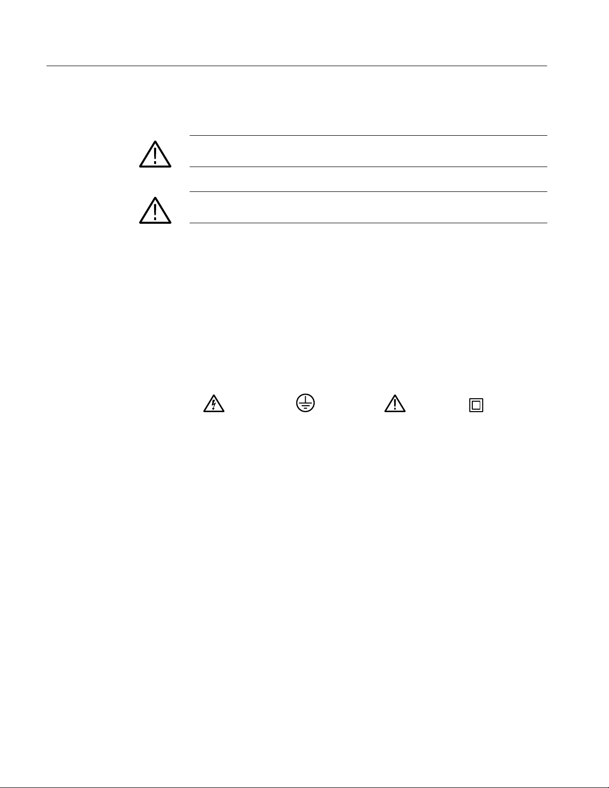
Symbols on the Product. The following symbols may appear on the product:
WARNING
High Voltage
Protective Ground
(Earth) T erminal
CAUTION
Refer to Manual
Double
Insulated
iv
TMS 562 MPC8260 Microprocessor Support
Page 9

Preface
This instruction manual contains specific information about the
TMS 562 MPC8260 microprocessor support package and is part of a set of
information on how to operate this product on compatible Tektronix logic
analyzers.
If you are familiar with operating microprocessor support packages on the logic
analyzer for which the TMS 562 MPC8260 support was purchased, you will
probably only need this instruction manual to set up and run the support.
If you are not familiar with operating microprocessor support packages, you will
need to supplement this instruction manual with information on basic operations
to set up and run the support.
Information on basic operations of microprocessor support packages is included
with each product. Each logic analyzer includes basic information that describes
how to perform tasks common to support packages on that platform. This
information can be in the form of online help, an installation manual, or a user
manual.
This manual provides detailed information on the following topics:
Manual Conventions
H Connecting the logic analyzer to the system under test
H Setting up the logic analyzer to acquire data from the system under test
H Acquiring and viewing disassembled data
This manual uses the following conventions:
H The term “disassembler” refers to the software that disassembles bus cycles
into instruction mnemonics and cycle types.
H The phrase “information on basic operations” refers to online help, an
installation manual, or a user manual covering the basic operations of
microprocessor support.
H In the information on basic operations, the term “XXX” or “P54C” appearing
in field selections and file names must be replaced with MPC8260. This term
is the name of the microprocessor in field selections and file names you must
use to operate the MPC8260 support.
TMS 562 MPC8260 Microprocessor Support
v
Page 10

Preface
Contacting Tektronix
Product
Support
Service
Support
For other
information
To write us
Website
For questions about using Tektronix measurement products, call
toll free in North America:
1-800-TEK-WIDE (1-800-835-9433 ext. 2400)
6:00 a.m. – 5:00 p.m. Pacific time
Or contact us by e-mail:
tm_app_supp@tek.com
For product support outside of North America, contact your
local Tektronix distributor or sales office.
Tektronix offers extended warranty and calibration programs as
options on many products. Contact your local Tektronix
distributor or sales office.
For a listing of worldwide service centers, visit our web site.
In North America:
1-800-TEK-WIDE (1-800-835-9433)
An operator will direct your call.
Tektronix, Inc.
P.O. Box 1000
Wilsonville, OR 97070-1000
USA
Tektronix.com
vi
TMS 562 MPC8260 Microprocessor Support
Page 11

Getting Started
Page 12

Page 13

Getting Started
This chapter contains information on the TMS 562 MPC8260 microprocessor
support and information on connecting your logic analyzer to your system under
test.
Support Package Description
The TMS 562 MPC8260 microprocessor support package displays disassembled
data from systems based on the Motorola MPC8260 microprocessor.
To use this support efficiently, refer to information on basic operations and the
following documents:
H MPC8260 PowerQUICC II User’s Manual March/1999 Rev. x.4
Logic Analyzer Software Compatibility
The label on the microprocessor support floppy disk states the version of logic
analyzer software the support is compatible with.
Logic Analyzer Configuration
The TMS 562 support requires a minimum of one 136-channel module.
Requirements and Restrictions
Review the electrical specifications in the Specifications chapter in this manual
as they pertain to your system under test, as well as the following descriptions of
other MPC8260 support requirements and restrictions.
Hardware Reset. If a hardware reset occurs in your MPC8260 system during an
acquisition, the application disassembler might acquire an invalid sample.
System Clock Rate. The MPC8260 microprocessor support can acquire data from
the MPC8260 microprocessor operating at speeds of 100 – 200 MHz. The
MPC8260 microprocessor support has been tested at the clock rate of 66 MHz.
The operating clock rate specifications were measured at the time of printing.
Contact your Tektronix sales representative for current information on the fastest
devices supported.
TMS 562 MPC8260 Microprocessor Support
1–1
Page 14

Getting Started
Alternate Bus Master Cycles. The TMS 562 support acquires all bus cycles. The
disassembler can distinguish between the MPC8260 cycle and the alternate
master cycle by looking at the BG~ signal.
Nonintrusive Acquisition. The MPC8260 microprocessor will not intercept,
modify, or present signals back to the system under test.
Disabling the Instruction Cache. To display disassembled acquired data, you must
disable the internal instruction cache. Disabling the cache makes all instruction
prefetches visible on the bus so that they can be acquired and displayed
disassembled.
Disabling the Data Cache. To display acquired data, you must disable the data
cache. Disabling the data cache makes visible all loads and stores to memory on
the bus, including data reads and writes, so the software can acquire and display
them.
Address Translation. The address translation must be turned off for proper
disassembly.
1–2
TMS 562 MPC8260 Microprocessor Support
Page 15

Functionality Not Supported
Interrupt Signals. Not all interrupt signals are acquired by the TMS 562 support
software. The interrupt signals that are acquired can be identified by the
TMS 562 support software by looking at the address that is displayed for the
interrupt service.
CPM Cycles. The communication processor module (CPM) is not supported.
60x Bus. Only the 60x bus is supported. The local bus of the processor is not
supported.
Nonintrusive Acquisition. The MPC8260 microprocessor will not intercept,
modify, or present signals back to the system under test.
Address Retry Cycles. Address Retry cycles are not supported.
Getting Started
Transfer Error Cycles. Transfer Error cycles are not supported.
SDRAM Address Multiplexing. SDRAM address multiplexing is not supported.
Connecting the Logic Analyzer to a System Under Test
You can use channel probes, clock probes, and leadsets with a commercial test
clip (or adapter) to make connections between the logic analyzer and your system
under test.
To connect the probes to MPC8260 signals in the system under test using a test
clip, follow these steps:
1. Power off your system under test. It is not necessary to power off the logic
analyzer.
CAUTION. To prevent static damage, handle these components only in a staticfree environment. Static discharge can damage the microprocessor, the probes,
and the logic analyzer module.
Always wear a grounding wrist strap, heel strap, or similar device while
handling the microprocessor.
TMS 562 MPC8260 Microprocessor Support
1–3
Page 16

Getting Started
Channel Assignments
2. To discharge your stored static electricity, touch the ground connector located
on the back of the logic analyzer. If you are using a test clip, touch any of the
ground pins on the clip to discharge stored static electricity from the test clip.
CAUTION. To prevent permanent damage to the pins on the microprocessor place
the system under test on a horizontal surface before connecting the test clip.
3. Place the system under test on a horizontal, static-free surface.
4. Use Table 1–1 through Table 1–8 to connect the channel probes to MPC8260
signal pins on the test clip or in the system under test.
5. Use leadsets to connect at least one ground lead from each channel probe and
the ground lead from each clock probe to ground pins on your test clip.
Channel assignments listed in Table 1–1 through Table 1–8 use the following
conventions:
H All signals are required by the support unless indicated otherwise.
H Channels are listed starting with the most significant bit (MSB) and
descending to the least significant bit (LSB).
H Channel group assignments are for all modules unless otherwise noted.
H A tilde symbol (~) following the signal name indicates an active low signal.
H The module in the higher-numbered slot is referred to as the HI module and
the module in the lower-numbered slot is referred to as the LO module.
The TLA 704 logic analyzer has the lower-numbered slots on the top and the
TLA 711 logic analyzer has the lower-numbered slots on the left.
1–4
TMS 562 MPC8260 Microprocessor Support
Page 17

Getting Started
Table 1–1 lists the bit order, probe section and channel assignments for the
Address group and the microprocessor signal for each channel connect. By
default, this channel group is displayed in hexadecimal.
T able 1–1: Address channel group assignments
Bit order Section:channel MPC8260 signal name
0 A0:0 A0
1 A0:1 A1
2 A0:2 A2
3 A0:3 A3
4 A0:4 A4
5 A0:5 A5
6 A0:6 A6
7 A0:7 A7
8 A1:0 A8
9 A1:1 A9
10 A1:2 A10
11 A1:3 A11
12 A1:4 A12
13 A1:5 A13
14 A1:6 A14
15 A1:7 A15
16 A2:0 A16
17 A2:1 A17
18 A2:2 A18
19 A2:3 A19
20 A2:4 A20
21 A2:5 A21
22 A2:6 A22
23 A2:7 A23
24 A3:0 A24
25 A3:1 A25
26 A3:2 A26
27 A3:3 A27
28 A3:4 A28
29 A3:5 A29
30 A3:6 A30
31 A3:7 A31
TMS 562 MPC8260 Microprocessor Support
1–5
Page 18

Getting Started
TraceAddr group Assignments. This is a synthesized group. This is used for
tracking the program flow when the cache is enabled. The user needs to use this
in conjuntion with the Trace Writes in Use disassembly option set to YES. This
group also uses the Trace Write Address value in the disassembly option which
needs to be entered by the user.
The user needs to enable the Branch Trace Exception by setting the BE field in
the MSR of MPC8260. When the Branch Trace Exception subroutine is
encountered, the SRR0 register will contain the target address of the branch
which was just executed. In the Trace Exception subroutine, the user would need
to write the value stored in SRR0 into the address specified in Trace Write
Address field. This needs to be a 32–bit write since the address is 32–bits.
Once this is done, the TraceAddr field would contain the value of the written data
which points to the target of the branch instruction. This is done by copying the
contents of the High_Data group into the TraceAddr group field. This can be
used for tracking the program flow even when cache is enabled.
NOTE. The Trace Write Address needs to be double word aligned, and located in
a 32–bit or a 64–bit memory region.
1–6
TMS 562 MPC8260 Microprocessor Support
Page 19

Getting Started
Table 1–2 lists the bit order, probe section and channel assignments for the High
Data group and the microprocessor signal for each channel connect. By default,
this channel group is displayed in hexadecimal.
T able 1–2: High Data channel group assignments
Bit order Section:channel MPC8260 signal name
0 E0:0 D0
1 E0:1 D1
2 E0:2 D2
3 E0:3 D3
4 E0:4 D4
5 E0:5 D5
6 E0:6 D6
7 E0:7 D7
8 E1:0 D8
9 E1:1 D9
10 E1:2 D10
11 E1:3 D11
12 E1:4 D12
13 E1:5 D13
14 E1:6 D14
15 E1:7 D15
16 E2:0 D16
17 E2:1 D17
18 E2:2 D18
19 E2:3 D19
20 E2:4 D20
21 E2:5 D21
22 E2:6 D22
23 E2:7 D23
24 E3:0 D24
25 E3:1 D25
26 E3:2 D26
27 E3:3 D27
28 E3:4 D28
29 E3:5 D29
30 E3:6 D30
31 E3:7 D31
TMS 562 MPC8260 Microprocessor Support
1–7
Page 20

Getting Started
Table 1–3 lists the bit order, probe section and channel assignments for the Low
Data group, and the microprocessor signal for each channel connect. By default,
this channel group is displayed in hexadecimal.
T able 1–3: Low Data channel group assignments
Bit order Section:channel MPC8260 signal name
32 D0:0 D32
33 D0:1 D33
34 D0:2 D34
35 D0:3 D35
36 D0:4 D36
37 D0:5 D37
38 D0:6 D38
39 D0:7 D39
40 D1:0 D40
41 D1:1 D41
42 D1:2 D42
43 D1:3 D43
44 D1:4 D44
45 D1:5 D45
46 D1:6 D46
47 D1:7 D47
48 D2:0 D48
49 D2:1 D49
50 D2:2 D50
51 D2:3 D51
52 D2:4 D52
53 D2:5 D53
54 D2:6 D54
55 D2:7 D55
56 D3:0 D56
57 D3:1 D57
58 D3:2 D58
59 D3:3 D59
60 D3:4 D60
61 D3:5 D61
62 D3:6 D62
63 D3:7 D63
1–8
TMS 562 MPC8260 Microprocessor Support
Page 21
Getting Started
Table 1–4 lists the probe section and channel assignments of the Control group,
and the microprocessor signal for each channel connect. The default radix of the
Control group is SYMBOLIC on the TLA 700. The symbol table file name is
MPC8260_Ctrl. By default, this channel group is displayed as symbols.
T able 1–4: Control channel group assignments
Section:channel MPC8260 signal name
C2:1 BG~
C2:3 TS~
CLK:1 ABB~/IRQ2~
C2:7 AACK~
CLK:2 ARTRY~
CLK:3 TEA~
C2:2 PSDV AL~
C3:3 TA~
C3:5 BCTL0~
QUAL:3 POE~/PSDRAS~/PGPL2
QUAL:2 PSDCAS~/PGPL3~
Table 1–5 lists the probe section and channel assignments for the Tsize group and
the microprocessor signal for each channel connect. The symbol table file name
is MPC8260_Tsiz. By default, this channel group is displayed as symbols.
T able 1–5: Tsize channel group assignments
Section:channel MPC8260 signal name
C2:0 TBST~
C0:1 TSIZ0
C0:5 TSIZ1
C1:1 TSIZ2
C1:5 TSIZ3
TMS 562 MPC8260 Microprocessor Support
1–9
Page 22
Getting Started
Table 1–6 lists the probe section and channel assignments for the Transfer group
and the microprocessor signal for each channel connect. The symbol table file
name is MPC8260_Tran. By default, this channel group is displayed as hex.
T able 1–6: Transfer Type channel group assignments
Section:channel MPC8260 signal name
C0:0 TT0
C0:4 TT1
C1:0 TT2
C1:4 TT3
C0:2 TT4
Table 1–7 lists the probe section and channel assignments for the
PWE/PSDDQM/PBS[0-7]~ group and the microprocessor signal for each
channel connect. By default, this channel group is displayed as hex.
T able 1–7: PWE…channel group assignments
Section:channel MPC8260 signal name
C0:3 PWE0~/PSDDQM0~/PBS0~
C0:7 PWE1~/PSDDQM1~/PBS1~
C1:3 PWE2~/PSDDQM2~/PBS2~
C1:7 PWE3~/PSDDQM3~/PBS3~
C2:4 PWE4~/PSDDQM4~/PBS4~
C3:0 PWE5~/PSDDQM5~/PBS5~
C3:4 PWE6~/PSDDQM6~/PBS6~
C2:5 PWE7~/PSDDQM7~/PBS7~
1–10
TMS 562 MPC8260 Microprocessor Support
Page 23
Getting Started
Table 1–8 lists the probe section and channel assignments for the Misc group and
the microprocessor signal for each channel connect. By default, this channel
group is displayed as hex.
T able 1–8: Misc channel group assignments
Section:channel MPC8260 signal name
CLK:0 CLKIN
C3:1 PSDA10/PGPL0
C3:2 HRESET~
C2:6 SRESET~
C3:6 RSTCONF~
C3:7 IRQ4~/DP4/CORE_SRESET~/EXT_BG3~
C0:6 BNKSEL0/TC0/AP1/MODCK1
C1:2 BNKSEL1/TC1/AP2/MODCK2
C1:6 BNKSEL2/TC2/AP3/MODCK3
Table 1–9 lists the probe section and channel assignments for the clock probes
(not part of any group), and theMPC8260 signal to which each channel connects.
T able 1–9: Clock and qualifier channel assignments
Section:
channel
CLK:0 Rising CLKIN Clock
CLK:1 NA ABB~/IRQ2~ Qualifier
CLK:2 NA ARTRY~ Qualifier
CLK:3 NA TEA~ Qualifier
C2:0 NA TBST~ Qualifier
C2:1 NA BG~ Qualifier
C2:2 NA PSDV AL~ as QUAL Qualifier
C2:3 NA TS~ as QUAL Qualifier
QUAL:0 NA Not Connected 102 & 136 Channel
QUAL:1 NA Not Connected 102 & 136 Channel
QUAL:2 NA PSDCAS~/PGPL3 136 Channel only
QUAL:3 NA POE~/PSDRAS~/PGPL2 136 Channel only
Active CLK edge
MPC8260
signal name
Description
The CLK channels and QUAL channels are stored as acquisition data and can be
used for triggering.
TMS 562 MPC8260 Microprocessor Support
1–11
Page 24

Getting Started
Table 1–10 lists the MPC8260 signals required by the Clocking State Machine
(CSM) and disassembler for clocking and disassembly. They may be removed
from their default connections and reattached to other signals of interest.
T able 1–10: Channel groups required for clocking and
disassembly
MPC8260
signal name
A0-A31 (Address Group) A0:0-7
D0-D63 E0:0-7
(High_Data and E1:0-7
Low_Data Groups) E2:0-7
Section:channel
A1:0-7
A2:0-7
A3:0-7
E3:0-7
D0:0-7
D1:0-7
D2:0-7
D3:0-7
CLKIN CLK:0
TS~ C2:3
PSDV AL~ C2:2
BG~ C2:1
TBST~ C2:0
PSDCAS~/PGPL3 QUAL:2
POE~/PSDRAS~/PGPL2 QUAL:3
TSIZ3 C1:5
TT3 C1:4
TSIZ2 C1:1
TT2 C1:0
TSIZ1 C0:5
1–12
TT1 C0:4
TT4 C0:2
TSIZ0 C0:1
TT0 C0:0
TMS 562 MPC8260 Microprocessor Support
Page 25

Getting Started
Table 1–11 lists channel groups not required for clocking and disassembly by the
MPC8260
microprocessor support. They may be removed from their default
connections and reattached to other signals of interest.
T able 1–11: Channel groups not required for clocking
and disassembly
Section:
channel
CLK:1 ABB~/IRQ2~
CLK:2 AR TR Y~
CLK:3 TEA~
QUAL:0 No Connection
QUAL:1 No Connection
C3:7 IRQ4~/DP4/CORE_SRESET~/EXT_BG3~
C3:6 RSTCONF~
C3:5 BCTL0~
C3:4 PWE6~/PSDDQM6~/PBS6~
C3:3 TA~
C3:2 HRESET~
C3:1 PSDA10/PGPL0
C3:0 PWE5~/PSDDQM5~/PBS5~
C2:7 AACK~
C2:6 SRESET~
C2:5 PWE7~/PSDDQM7~/PBS7~
MPC8260
signal name
C2:4 PWE4~/PSDDQM4~/PBS4~
C1:7 PWE3~/PSDDQM3~/PBS3~
C1:6 BNKSEL2/TC2/AP3/MODCK3
C1:3 PWE2~/PSDDQM2~/PBS2~
C1:2 BNKSEL1/TC1/AP2/MODCK2
C0:7 PWE1~/PSDDQM1~/PBS1~
C0:6 BNKSEL0/TC0/AP1/MODCK1
C0:3 PWE0~/PSDDQM0~/PBS0~
TMS 562 MPC8260 Microprocessor Support
1–13
Page 26

Getting Started
Table 1–12 lists signals not on the probe adapter. If, you require access to these
signals, another way must be found to probe these signals.
T able 1–12: Signals not on the probe adapter
MPC8260
pin number
t2 ALE
t5 BADDR[27]
u1 BADDR[28]
u2 BADDR[29]
u3 BADDR[30]
u4 BADDR[31]
y3 CPU_BR~
r2 CPU_DBG~
f25 CS[0]
c29 CS[1]
e27 CS[2]
e28 CS[3]
f26 CS[4]
f27 CS[5]
f28 CS[6]
g25 CS[7]
MPC8260
signal name
1–14
d29 CS[8]
e29 CS[9]
f29 CS[10]
g28 CS[11]
b22 DP[0]
a22 DP[1]
e21 DP[2]
d21 DP[3]
b21 DP[5]
a21 DP[6]
e20 DP[7]
w1 GBL~
y4 L2_HIT~
TMS 562 MPC8260 Microprocessor Support
Page 27

T able 1–12: Signals not on the probe adapter (Cont.)
Getting Started
MPC8260
pin number
n27 LA[14]
t29 LA[15]
r27 LA[16]
r26 LA[17]
r29 LA[18]
r28 LA[19]
w29 LA[20]
p28 LA[21]
n26 LA[22]
aa27 LA[23]
p29 LA[24]
aa26 LA[25]
n25 LA[26]
aa25 LA[27]
ab29 LA[28]
ab28 LA[29]
MPC8260
signal name
p25 LA[30]
ab27 LA[31]
h29 LCLD[0]
j29 LCLD[1]
j28 LCLD[2]
j27 LCLD[3]
j26 LCLD[4]
j25 LCLD[5]
k25 LCLD[6]
l29 LCLD[7]
l27 LCLD[8]
l26 LCLD[9]
l25 LCLD[10]
m29 LCLD[1 1]
m28 LCLD[12]
m27 LCLD[13]
TMS 562 MPC8260 Microprocessor Support
1–15
Page 28

Getting Started
T able 1–12: Signals not on the probe adapter (Cont.)
MPC8260
pin number
m26 LCLD[14]
n29 LCLD[15]
t25 LCLD[16]
u27 LCLD[17]
u26 LCLD[18]
u25 LCLD[19]
v29 LCLD[20]
v28 LCLD[21]
v27 LCLD[22]
v26 LCLD[23]
w27 LCLD[24]
w26 LCLD[25]
w25 LCLD[26]
y29 LCLD[27]
y28 LCLD[28]
y25 LCLD[29]
MPC8260
signal name
aa29 LCLD[30]
aa28 LCLD[31]
l28 LCLDP[0]
n28 LCLDP[1]
t28 LCLDP[2]
w28 LCLDP[3]
c26 LGTA
e26 LOE~
d27 LSDA10
b27 LSDAMUX~
d25 LSDCAS~
c28 LSDWE~
h28 LWE[0]~
h27 LWE[1]~
h26 LWE[2]~
g29 LWE[3]~
1–16
TMS 562 MPC8260 Microprocessor Support
Page 29

T able 1–12: Signals not on the probe adapter (Cont.)
Getting Started
MPC8260
pin number
d28 LWR~
ac29 PA0
ac25 PA1
ae28 PA2
ag29 PA3
ag28 PA4
ag26 PA5
ae24 PA6
ah25 PA7
af23 PA8
ah23 PA9
ae22 PA10
ah22 PA11
aj21 PA12
ah20 PA13
ag19 PA14
MPC8260
signal name
af18 PA15
af17 PA16
ae16 PA17
aj16 PA18
ag15 PA19
aj13 PA20
ae13 PA21
af12 PA22
ag1 1 PA23
ah9 PA24
aj8 PA25
ah7 PA26
af7 PA27
ad5 PA28
af1 PA29
ad3 PA30
TMS 562 MPC8260 Microprocessor Support
1–17
Page 30

Getting Started
T able 1–12: Signals not on the probe adapter (Cont.)
MPC8260
pin number
ab5 PA31
ad28 PB4
ad26 PB5
ad25 PB6
ae26 PB7
ah27 PB8
ag24 PB9
ah24 PB10
aj24 PB11
ag22 PB12
ah21 PB13
ag20 PB14
af19 PB15
aj18 PB16
aj17 PB17
ae14 PB18
MPC8260
signal name
af13 PB19
ag12 PB20
ah1 1 PB21
ah16 PB22
ae15 PB23
aj9 PB24
ae9 PB25
aj7 PB26
ah6 PB27
ae3 PB28
ae2 PB29
ac5 PB30
ac4 PB31
ab26 PC0
ad29 PC1
ae29 PC2
1–18
TMS 562 MPC8260 Microprocessor Support
Page 31

T able 1–12: Signals not on the probe adapter (Cont.)
Getting Started
MPC8260
pin number
ae27 PC3
af27 PC4
af24 PC5
aj26 PC6
aj25 PC7
af22 PC8
ae21 PC9
af20 PC10
ae19 PC11
ae18 PC12
ah18 PC13
ah17 PC14
ag16 PC15
af15 PC16
aj15 PC17
ah14 PC18
MPC8260
signal name
ag13 PC19
ah12 PC20
aj1 1 PC21
ag10 PC22
ae10 PC23
af9 PC24
ae8 PC25
aj6 PC26
ag2 PC27
af3 PC28
af2 PC29
ae1 PC30
ad1 PC31
ac28 PD4
ad27 PD5
af29 PD6
TMS 562 MPC8260 Microprocessor Support
1–19
Page 32

Getting Started
T able 1–12: Signals not on the probe adapter (Cont.)
MPC8260
pin number
af28 PD7
ag25 PD8
ah26 PD9
aj27 PD10
aj23 PD11
ag23 PD12
aj22 PD13
ae20 PD14
aj20 PD15
ag18 PD16
ag17 PD17
af16 PD18
ah15 PD19
aj14 PD20
ah13 PD21
aj12 PD22
MPC8260
signal name
ae12 PD23
af10 PD24
ag9 PD25
ah8 PD26
ag7 PD27
ae4 PD28
ag1 PD29
ad4 PD30
ad2 PD31
a23 PGTA~
ag6 PORESET~
d22 PSDAMUX~
aa3 QREQ
aa1 TERM[0]
ag4 TERM[1]
1–20
TMS 562 MPC8260 Microprocessor Support
Page 33

T able 1–12: Signals not on the probe adapter (Cont.)
Getting Started
MPC8260
pin number
ab4 TRIS
ab2 XFC
MPC8260
signal name
Table 1–13 lists extra acquisition channels not on the probe adapter by default.
T able 1–13: Channels not on the probe adapter
TLA clock channel MPC8260 pin number
QUAL:[1-0] Not connected
Acquisition Setup. The MPC8260 support will affect the logic analyzer setup
menus and submenus by modifying existing fields and adding micro-specific
fields.
The MPC8260 support will add the selection MPC8260 to the Load Support
Package dialog box, located under the File pulldown menu. Once that MPC8260
support has been loaded, the Custom clocking mode selection in the logic
analyzer module Setup menu is also enabled.
TMS 562 MPC8260 Microprocessor Support
1–21
Page 34

Getting Started
Channel Charts
Tables 1–14 through 1–19 identify the signal names assigned to the acquisition
channel numbers on the logic analyzer.
T able 1–14: Clock channels
TLA clock
channel
CLK:3 – M TEA~
CLK:2 – M ARTRY~
CLK:1 – M ABB~/IRQ2~
CLK:0 CLK Rising M CLKIN
CLK or
Qual
Active
CLK edge
Login
strobe
MPC8260 signal name
T able 1–15: Qual channels
TLA clock
channel
QUAL:3 QUAL – M POE~/PSDRAS~/PGPL2
QUAL:2 QUAL – M PSDCAS~/PGPL3
QUAL:1 – M
QUAL:0 – M
Qual only
Active
CLK edge
Login
strobe
MPC8260 signal name
1–22
TMS 562 MPC8260 Microprocessor Support
Page 35

T able 1–16: Address channels
Getting Started
TLA acquisition
channel
A3:7 LOGA7 A_SDRAM A31
A3:6 LOGA7 A_SDRAM A30
A3:5 LOGA7 A_SDRAM A29
A3:4 LOGA7 A_SDRAM A28
A3:3 LOGA6 A_SDRAM A27
A3:2 LOGA6 A_SDRAM A26
A3:1 LOGA6 A_SDRAM A25
A3:0 LOGA6 A_SDRAM A24
A2:7 LOGA5 A_SDRAM A23
A2:6 LOGA5 A_SDRAM A22
A2:5 LOGA5 A_SDRAM A21
A2:4 LOGA5 A_SDRAM A20
A2:3 LOGA4 A_SDRAM A19
A2:2 LOGA4 A_SDRAM A18
A2:1 LOGA4 A_SDRAM A17
A2:0 LOGA4 A_SDRAM A16
A1:7 LOGA3 A_SDRAM A15
A1:6 LOGA3 A_SDRAM A14
A1:5 LOGA3 A_SDRAM A13
A1:4 LOGA3 A_SDRAM A12
A1:3 LOGA2 A_SDRAM A11
A1:2 LOGA2 A_SDRAM A10
A1:1 LOGA2 A_SDRAM A9
A1:0 LOGA2 A_SDRAM A8
A0:7 LOGA1 A_SDRAM A7
A0:6 LOGA1 A_SDRAM A6
A0:5 LOGA1 A_SDRAM A5
A0:4 LOGA1 A_SDRAM A4
A0:3 LOGA0 A_SDRAM A3
A0:2 LOGA0 A_SDRAM A2
A0:1 LOGA0 A_SDRAM A1
A0:0 LOGA0 A_SDRAM A0
Login
group
Login
strobe
MPC8260 signal name
TMS 562 MPC8260 Microprocessor Support
1–23
Page 36

Getting Started
T able 1–17: Control channels
TLA acquisition
channel
C3:7 LOGC7 M IRQ4~/DP4/CORE_SRESET~/EXT_BG3~
C3:3 LOGC7 M TA~
C2:7 LOGC7 M AACK~
C2:3# LOGC7 TS_BG TS~
C3:6 LOGC6 M RSTCONF~
C3:2 LOGC6 M HRESET~
C2:6 LOGC6 M SRESET~
C2:2# LOGC6 M PSDVAL~
C3:5 LOGC5 M BCLT0~
C3:1 LOGC5 M PSDA10/PGPL0
C2:5 LOGC5 M PWE7~/PSDDQM7~/PBS7
C2:1 LOGC5 TS_BG BG~
C3:4 LOGC4 M PWE6~/PSDDQM6~/PBS6~
C3:0 LOGC4 M PWE5~/PSDDQM5~/PBS5~
C2:4 LOGC4 M PWE4~/PSDDQM4~/PBS4~
C2:0 LOGC4 M TBST~
C1:7 LOGC3 M PWE3~/PSDDQM3~/PBS3~
C1:3 LOGC3 M PWE2~/PSDDQM2~/PBS2~
C0:7 LOGC3 M PWE1~/PSDDQM1~/PBS1~
C0:3 LOGC3 M PWE0~/PSDDQM0~/PBS0~
C1:6 LOGC2 M BNKSEL2/TC2/AP3/MODCK3
C1:2 LOGC2 M BNKSEL1/TC1/AP2/MODCK2
C0:6 LOGC2 M BNKSEL0/TC0/AP1/MODCK1
C0:2 LOGC2 M TT4
C1:5 LOGC1 M TSIZ3
C1:1 LOGC1 M TSIZ2
C0:5 LOGC1 M TSIZ1
C0:1 LOGC1 M TSIZ0
C1:4 LOGC0 M TT3
C1:0 LOGC0 M TT2
C0:4 LOGC0 M TT1
C0:0 LOGC0 M TT0
Login
group
Login
strobe
MPC8260 signal name
1–24
TMS 562 MPC8260 Microprocessor Support
Page 37

T able 1–18: Data channels
Getting Started
TLA acquisition
channel
D3:7 LOGD7 M D63
D3:6 LOGD7 M D62
D3:5 LOGD7 M D61
D3:4 LOGD7 M D60
D3:3 LOGD6 M D59
D3:2 LOGD6 M D58
D3:1 LOGD6 M D57
D3:0 LOGD6 M D56
D2:7 LOGD5 M D55
D2:6 LOGD5 M D54
D2:5 LOGD5 M D53
D2:4 LOGD5 M D52
D2:3 LOGD4 M D51
D2:2 LOGD4 M D50
D2:1 LOGD4 M D49
D2:0 LOGD4 M D48
D1:7 LOGD3 M D47
D1:6 LOGD3 M D46
D1:5 LOGD3 M D45
D1:4 LOGD3 M D44
D1:3 LOGD2 M D43
D1:2 LOGD2 M D42
D1:1 LOGD2 M D41
D1:0 LOGD2 M D40
D0:7 LOGD1 M D39
D0:6 LOGD1 M D38
D0:5 LOGD1 M D37
D0:4 LOGD1 M D36
D0:3 LOGD0 M D35
D0:2 LOGD0 M D34
D0:1 LOGD0 M D33
D0:0 LOGD0 M D32
Login
group
Login
strobe
MPC8260 signal name
TMS 562 MPC8260 Microprocessor Support
1–25
Page 38

Getting Started
T able 1–19: Extended Data channels
TLA acquisition
channel
E3:7 LOGE7 M D31
E3:6 LOGE7 M D30
E3:5 LOGE7 M D29
E3:4 LOGE7 M D28
E3:3 LOGE6 M D27
E3:2 LOGE6 M D26
E3:1 LOGE6 M D25
E3:0 LOGE6 M D24
E2:7 LOGE5 M D23
E2:6 LOGE5 M D22
E2:5 LOGE5 M D21
E2:4 LOGE5 M D20
E2:3 LOGE4 M D19
E2:2 LOGE4 M D18
E2:1 LOGE4 M D17
E2:0 LOGE4 M D16
E1:7 LOGE3 M D15
E1:6 LOGE3 M D14
E1:5 LOGE3 M D13
E1:4 LOGE3 M D12
E1:3 LOGE2 M D11
E1:2 LOGE2 M D10
E1:1 LOGE2 M D9
E1:0 LOGE2 M D8
E0:7 LOGE1 M D7
E0:6 LOGE1 M D6
E0:5 LOGE1 M D5
E0:4 LOGE1 M D4
E0:3 LOGE0 M D3
E0:2 LOGE0 M D2
E0:1 LOGE0 M D1
E0:0 LOGE0 M D0
Login
group
Login
strobe
MPC8260 signal name
1–26
TMS 562 MPC8260 Microprocessor Support
Page 39

CPU To Mictor Connections
To probe the microprocessor you will need to make connections between the
CPU and the Mictor pins of the P6434 Mass Termination Probe. Refer to the
P6434 Mass Termination Probe Manual, Tektronix part number 070-9793-xx, for
more information on mechanical specifications. Tables 1–20 through 1–23 show
the CPU pin to Mictor pin connections.
Tektronix uses a counterclockwise pin assignment. Pin-1 is located at the top left,
and pin-2 is located directly below it. Pin-20 is located on the bottom right, and
pin-21 is located directly above it.
AMP uses an odd side-even side pin assignment. Pin-1 is located at the top left,
and pin-3 is located directly below it. Pin-2 is located on the top right, and pin-4
is located directly below it (see Figure 1–1).
NOTE. When designing Mictor connectors into your system under test, always
follow the Tektronix pin assignment.
Getting Started
Tektronix Pinout AMP Pinout
Pin 1
Pin 19
Pin 38
Pin 20
Pin 1
Pin 37
Pin 2
Pin 38
Figure 1–1: Pin assignments for a Mictor connector (component side)
T able 1–20: CPU to Mictor connections for Mictor A pins
Tektronix
Mictor A
pin number
1 1 GND GND GND
2 3 GND GND GND
3 5 CLK:0 CLKIN ah4
4 7 A3:7 A31 r4
5 9 A3:6 A30 r5
6 11 A3:5 A29 r3
7 13 A3:4 A28 r1
AMP
Mictor A
pin number
LA Channel
MPC8260
signal name
MPC8260
pin number
TMS 562 MPC8260 Microprocessor Support
1–27
Page 40

Getting Started
T able 1–20: CPU to Mictor connections for Mictor A pins (Cont.)
Tektronix
Mictor A
pin number
8 15 A3:3 A27 p1
9 17 A3:2 A26 p2
10 19 A3:1 A25 p3
11 21 A3:0 A24 p4
12 23 A2:7 A23 n1
13 25 A2:6 A22 n2
14 27 A2:5 A21 n3
15 29 A2:4 A20 n4
16 31 A2:3 A19 n5
17 33 A2:2 A18 m5
18 35 A2:1 A17 l1
19 37 A2:0 A16 l2
20 38 A0:0 A0 g1
21 36 A0:1 A1 h5
22 34 A0:2 A2 h2
23 32 A0:3 A3 h1
24 30 A0:4 A4 j5
25 28 A0:5 A5 j4
26 26 A0:6 A6 j3
27 24 A0:7 A7 j2
28 22 A1:0 A8 j1
29 20 A1:1 A9 k4
30 18 A1:2 A10 k3
31 16 A1:3 A11 k2
32 14 A1:4 A12 k1
33 12 A1:5 A13 l5
34 10 A1:6 A14 l4
35 8 A1:7 l5 l3
36 6 Clock:1 ABB~/IRQ2~ e2
37 4 GND GND GND
38 2 GND GND GND
39 39 GND GND GND
40 40 GND GND GND
41 41 GND GND GND
42 42 GND GND GND
AMP
Mictor A
pin number
LA Channel
MPC8260
signal name
MPC8260
pin number
1–28
TMS 562 MPC8260 Microprocessor Support
Page 41

T able 1–20: CPU to Mictor connections for Mictor A pins (Cont.)
Getting Started
Tektronix
Mictor A
pin number
43 43 GND GND GND
44 44 GND GND GND
AMP
Mictor A
pin number
LA Channel
MPC8260
signal name
MPC8260
pin number
T able 1–21: CPU to Mictor connections for Mictor D pins
Tektronix
Mictor D
pin number
1 1 GND GND GND
2 3 GND GND GND
3 5 NC – NC
4 7 D3:7 D63 c2
5 9 D3:6 D62 d6
6 11 D3:5 D61 e8
7 13 D3:4 D60 c10
AMP
Mictor D
pin number
LA Channel
MPC8260
signal name
MPC8260
pin number
8 15 D3:3 D59 d12
9 17 D3:2 D58 e14
10 19 D3:1 D57 b16
11 21 D3:0 D56 b18
12 23 D2:7 D55 d5
13 25 D2:6 D54 c6
14 27 D2:5 D53 a7
15 29 D2:4 D52 b10
16 31 D2:3 D51 c12
17 33 D2:2 D50 b14
18 35 D2:1 D49 e16
19 37 D2:0 D48 c18
20 38 D0:0 D32 e18
21 36 D0:1 D33 b17
22 34 D0:2 D34 a15
23 32 D0:3 D35 a12
TMS 562 MPC8260 Microprocessor Support
1–29
Page 42

Getting Started
T able 1–21: CPU to Mictor connections for Mictor D pins (Cont.)
Tektronix
Mictor D
pin number
24 30 D0:4 D36 d11
25 28 D0:5 D37 c8
26 26 D0:6 D38 e7
27 24 D0:7 D39 a3
28 22 D1:0 D40 d18
29 20 D1:1 D41 a17
30 18 D1:2 D42 a14
31 16 D1:3 D43 b12
32 14 D1:4 D44 a10
33 12 D1:5 D45 d8
34 10 D1:6 D46 b6
35 8 D1:7 D47 c4
36 6 Clock:2 ARTRY~ e1
37 4 GND GND GND
38 2 GND GND GND
AMP
Mictor D
pin number
LA Channel
MPC8260
signal name
MPC8260
pin number
39 39 GND GND GND
40 40 GND GND GND
41 41 GND GND GND
42 42 GND GND GND
43 43 GND GND GND
44 44 GND GND GND
T able 1–22: CPU to Mictor connections for Mictor E pins
Tektronix
Mictor E
pin number
1 1 GND GND GND
2 3 GND GND GND
3 5 QUAL:3 POE~/PSDRAS~/PGPL2 a24
4 7 E3:7 D31 e6
AMP
Mictor E
pin number
LA Channel
MPC8260
signal name
MPC8260
pin number
1–30
TMS 562 MPC8260 Microprocessor Support
Page 43

T able 1–22: CPU to Mictor connections for Mictor E pins (Cont.)
Getting Started
Tektronix
Mictor E
pin number
5 9 E3:6 D30 a4
6 11 E3:5 D29 b8
7 13 E3:4 D28 c11
8 15 E3:3 D27 d13
9 17 E3:2 D26 c15
10 19 E3:1 D25 c17
11 21 E3:0 D24 c19
12 23 E2:7 D23 c5
13 25 E2:6 D22 a5
14 27 E2:5 D21 a8
15 29 E2:4 D20 b11
16 31 E2:3 D19 c13
17 33 E2:2 D18 d15
18 35 E2:1 D17 d17
19 37 E2:0 D16 d19
AMP
Mictor E
pin number
LA Channel
MPC8260
signal name
MPC8260
pin number
20 38 E0:0 D0 b20
21 36 E0:1 D1 a18
22 34 E0:2 D2 a16
23 32 E0:3 D3 a13
24 30 E0:4 D4 e12
25 28 E0:5 D5 d9
26 26 E0:6 D6 a6
27 24 E0:7 D7 b5
28 22 E1:0 D8 a20
29 20 E1:1 D9 e17
30 18 E1:2 D10 b15
31 16 E1:3 D11 b13
32 14 E1:4 D12 a11
33 12 E1:5 D13 e9
34 10 E1:6 D14 b7
35 8 E1:7 D15 b4
TMS 562 MPC8260 Microprocessor Support
1–31
Page 44

Getting Started
T able 1–22: CPU to Mictor connections for Mictor E pins (Cont.)
Tektronix
Mictor E
pin number
36 6 QUAL:2 PSDCAS~/PGPL3 b23
37 4 GND GND GND
38 2 GND GND GND
39 39 GND GND GND
40 40 GND GND GND
41 41 GND GND GND
42 42 GND GND GND
43 43 GND GND GND
44 44 GND GND GND
AMP
Mictor E
pin number
LA Channel
MPC8260
signal name
MPC8260
pin number
T able 1–23: CPU to Mictor connections for Mictor C pins
Tektronix
Mictor C
pin number
1 1
2 3 GND GND GND
3 5 CLK:3 TEA~ v5
4 7 C3:7 IRQ4~/DP4/CORE_SRE-
5 9 C3:6 RSTCONF~ aj4
6 11 C3:5 BCLT0~ a27
7 13 C3:4 PWE6~/PSDDQM6~/PBS6~ b25
8 15 C3:3 TA~ c22
9 17 C3:2 HRESET~ ah5
10 19 C3:1 PSDA10/PGPL0 e23
11 21
12 23 C2:7 AACK~ f3
13 25 C2:6 SRESET~ b24
14 27 C2:5 PWE7~/PSDDQM7~/PBS7~ a25
15 29 C2:4 PWE4~/PSDDQM4~/PBS4~ b26
16 31 C2:3 TS~ e3
17 33 C2:2 PSDVAL~ v3
AMP
Mictor C
pin number
LA Channel
GND
C3:0
MPC8260
signal name
GND GND
SET~/EXT_BG3~
PWE5~/PSDDQM5~/PBS5~ a26
MPC8260
pin number
c21
1–32
TMS 562 MPC8260 Microprocessor Support
Page 45

T able 1–23: CPU to Mictor connections for Mictor C pins (Cont.)
Getting Started
Tektronix
Mictor C
pin number
18 35 C2:1 BG~ f4
19 37 C2:0 TBST~ d3
20 38 C0:0 TT0 f1
21 36 C0:1 TSIZ0 c1
22 34 C0:2 TT4 f2
23 32 C0:3 PWE0~/PSDDQM0~/PBS0~ c25
24 30 C0:4 TT1 g4
25 28 C0:5 TSIZ1 e4
26 26 C0:6 BNKSEL0/TC0/AP1/MODCK1 w2
27 24 C0:7 PWE1~/PSDDQM1~/PBS1~ e24
28 22 C1:0 TT2 g3
29 20 C1:1 TSIZ2 d2
30 18 C1:2 BNKSEL1/TC1/AP2/MODCK2 w3
31 16 C1:3 PWE2~/PSDDQM2~/PBS2~ d24
32 14 C1:4 TT3 g2
33 12 C1:5 TSIZ3 f5
34 10 C1:6 BNKSEL2/TC2/AP3/MODCK3 w4
35 8 C1:7 PWE3~/PSDDQM3~/PBS3~ c24
36 6 NC – NC
37 4 GND GND GND
38 2 GND GND GND
39 39 GND GND GND
40 40 GND GND GND
41 41 GND GND GND
42 42 GND GND GND
43 43 GND GND GND
44 44 GND GND GND
AMP
Mictor C
pin number
LA Channel
MPC8260
signal name
MPC8260
pin number
TMS 562 MPC8260 Microprocessor Support
1–33
Page 46

Getting Started
1–34
TMS 562 MPC8260 Microprocessor Support
Page 47

Operating Basics
Page 48

Page 49

Setting Up the Support
This section provides information on how to set up the support. The information
covers the following topics:
H Clocking options
H Symbol table files
The information in this section is specific to the operations and functions of the
TMS 562 MPC8260 support on any Tektronix logic analyzer for which it can be
purchased.
Before you acquire and display disassembled data, you need to load the support
and specify the setups for clocking and triggering as described in the information
on basic operations. The support provides default values for each of these setups,
but you can change them as needed.
Channel Group Definitions
The software automatically defines channel groups for the support. The channel
groups for the MPC8260 support are Address, Data, Tsize, Control, and Misc. If
you want to know which signal is in which group, refer to Channel Assignments
beginning on page 1–4.
TMS 562 MPC8260 Microprocessor Support
2–1
Page 50

Setting Up the Support
Clocking
This section provides information on clocking options for the MPC8260 support.
Custom Clocking
A special clocking program is loaded to the module every time you load the
MPC8260 support. This special clocking is called Custom.
When Custom is selected, the Custom Clocking Options menu has the subtitle
MPC8260 Microprocessor Clocking Support added, and clocking options are
displayed.
There are three clocking state machines (CSM)s:
H MPC8260I
H MPC8260II
H MPC8260III
The appropriate CSM is selected based on the user option given in the clocking
option menu.
H SDRAM and SRAM are supported in the MPC8260I CSM.
H DRAM and SRAM are supported in the MPC8260II CSM.
H SRAM only is supported in the MPC8260III CSM.
The clock edge is rising edge of the processor clock CLKIN. The qualifiers are
TS~, PSDVAL~, PSDCAS~/PGPL3 and POE~/PSDRAS~/PGPL2.
2–2
When using Custom clocking, the module logs signals from multiple-channel
groups at different times as they become valid on the MPC8260 bus. The module
then sends all the logged-in signals to the trigger machine and memory for
storage.
TMS 562 MPC8260 Microprocessor Support
Page 51

Setting Up the Support
Clocking Options
The TMS 562 support offers a microprocessor-specific clocking mode for the
MPC8260 microprocessor. This clocking mode is the default selection whenever
you load the MPC8260 support.
Disassembly will not be correct with the Internal or External clocking modes.
Information on basic operations describes how to use these clock selections for
general-purpose analysis. Following are the clocking options for MPC8260
support:
1. Memory Type Used
Selections available are:
H SDRAM and SRAM (default)
When the option ”SDRAM and SRAM” is selected, the SDRAM and SRAM
cycles will be supported. This requires that PSDCAS~/PGPL3 pin be used as
PSDCAS~ and the pin POE~/PSDRAS~/PGPL2 be used as PSDRAS~
H DRAM and SRAM
When the option ”DRAM and SRAM” is selected, the DRAM and SRAM
cycles will be supported.
H SRAM Only
When the option ”SRAM Only” is selected, only SRAM cycles will be
supported.
2. Pipeline Depth
Selections are:
H One (default)
H Zero
Based on whether the pipeline bit is set by the user in the BCR, this selection is
done.
NOTE. Incorrect results may occur if these options are not selected. The user-set
modes are very important and must be matched to the processor mode.
TMS 562 MPC8260 Microprocessor Support
2–3
Page 52

Setting Up the Support
Symbols
The TMS 562 support provides two symbol-table files. The MPC8260_Ctrl file
replaces specific Control-channel group values with symbolic values when
Symbolic is the radix for the channel group.
Table 2–1 lists the name, bit pattern, and description for the symbols in the file
MPC8260_Ctrl in the Control channel group symbol table.
T able 2–1: Control group symbol table definitions
Control group value
TS~
ABB~/IRQ2~
TAACK~ PSDVAL~
Symbol
END OF DATA CYCLE
DA TA CYCLE
TS~ ASSERTED
AACK~ ASSERTED
ARTRY~ ASSERTED
TEA~ ASSERTED
BCTL0~ ASSERTED
POE~/PSDRAS~/PGPL2
ASSERTED
PSDCAS~/PGPL3
ASSERTED
BG~ ASSERTED
BG~ TEA~ BCTL0~ PDSCAS~/PGPL3
X XXXXX X0X XX
X XXXXX 01X XX
X 0XXXX XXX XX
X XX0XX XXX XX
X XXX0X XXX XX
X XXXX0 XXX XX
X XXXXX XX0 XX
X XXXXX XXX 0X
X XXXXX XXX X0
0 XXXXX XXX XX
ARTRY~ TA~ PQE~/PSDRAS~/PGPL2
Description
TA~ signal asserted
PSDV AL~ signal asserted
TS~ signal asserted
AACK~ signal asserted
ARTRY~ signal asserted
TEA signal asserted
BCTL0 signal asserted
POE~/PSDRAS~/PGPL2
signal asserted
PSDCAS~/PGPL3 signal
asserted
BG~ signal asserted
2–4
TMS 562 MPC8260 Microprocessor Support
Page 53

Setting Up the Support
Table 2–2 lists the name, bit pattern, and description for the symbols in the file
MPC8260_Tsiz in the Tsize channel group symbol table.
T able 2–2: Tsize group symbol table definitions
Tsize group value
TBST* TSIZ2
Symbol
BYTE
HALF WORD
THREE BYTES
WORD
EXTENDED 5 BYTES
EXTENDED 6 BYTES
EXTENDED 7 BYTES
DOUBLE WORD
EXTENDED DOUBLE
DOUBLE WORD
EXTENDED TRIPLE
DOUBLE WORD
QUAD DOUBLE
WORD
UNKNOWN
TSIZ0 TSIZ3
TSIZ1
100 01
100 10
100 11
101 00
101 01
101 10
101 11
100 00
110 01
110 10
000 10
XXX XX
Description
Byte
Half Word
Three bytes
Word
Extended 5 bytes
Extended 6 bytes
Extended 7 bytes
Double Word
Extended double double word
Extended triple double word
Quad double word
Unknown
Information on basic operations describes how to use symbolic values for
triggering and for displaying other channel groups symbolically, such as for the
Address channel group.
Range Symbols. The TMS 562 design supports range symbols in a manner similar
to pattern symbols. Both types of symbols are accessed in the same manner (by
the user).
Range symbols associate a range of data values with a symbol name. When a
range symbol table is selected for the radix of the Address group, all address
values (both in the Address column and in the disassembly Mnemonics column)
will be replaced with their corresponding symbol name plus an offset, if the
value falls within one of the defined ranges. If no symbol is defined, the address
value will be displayed in hexadecimal or.octal, depending upon the output radix
selection for that symbol table. If the output radix selection is anything but HEX
or OCT, addresses will be displayed in hexadecimal. The offset (the difference
between the value and the lower bound of the range) will also be displayed in
that radix (hexadecimal or.octal).
TMS 562 MPC8260 Microprocessor Support
2–5
Page 54

Setting Up the Support
NOTE: The various ranges must not overlap.
For example, given the following disassembled code fragment:
Address Mnemonic
. .
00009700 b 0x 0A000F80
. .
. .
0A000F80 .
and given the Address group range symbol:
mysub 0x0A000F00
then displaying disassembly in Hardware mode and selecting symbolic radix for
the Address group will cause the following disassembled code fragment to be
displayed:
Address Mnemonic
. .
00970000 b mysub+80
. .
mysub+80 .
If the output radix of the symbol table is changed to OCTAL then the code
fragment will look like:
Address Mnemonic
. .
00970000 b mysub+200
. .
. .
mysub+200 .
Users can also load their own user-defined range symbols if the file follows the
conventions of the TLA 700 symbol table file format.
2–6
TMS 562 MPC8260 Microprocessor Support
Page 55

Acquiring and Viewing Disassembled Data
This section describes how to acquire data and view it disassembled. The
information covers the following topics and tasks:
H Acquiring data
H Viewing disassembled data in various display formats
H Labeling Cycle type
H Changing the way data is displayed
H Changing disassembled cycles with the mark cycles function
Acquiring Data
Once you load the MPC8260 support, choose a clocking mode, and specify the
trigger, you are ready to acquire and disassemble
If you have any problems acquiring data, refer to information on basic operations
in your online help or Appendix A: Error Messages and Disassembly Pr oblems in
the Basic Operations User Manual.
data.
Viewing Disassembled Data
You can view disassembled data in four display formats: Hardware, Software,
Control Flow, and Subroutine. The information on basic operations describes
how to select the disassembly display formats.
NOTE. Selections in the Disassembly property page must be set correctly for your
acquired data to be disassembled correctly. Refer to Changing How Data is
Displayed on page 2–11.
The default display format displays the Address, Data, Tsize, Control, and Misc,
channel group values for each sample of acquired data.
If a channel group is not visible, you must use the Disassembly property page to
make the group visible.
TMS 562 MPC8260 Microprocessor Support
2–7
Page 56

Acquiring and Viewing Disassembled Data
The disassembler displays special characters and strings in the instruction
mnemonics to indicate significant events. Table 2–3 lists these special characters
and strings and gives a definition of what they represent.
T able 2–3: Description of special characters in the display
Character or string displayed Definition
> Indicates there is insufficient room on the screen to show all
» The instruction was manually marked by the user using the
available data.
Mark Cycle function.
Hardware Display Format
In the hardware display format, all valid opcode fetch bus cycles will be
disassembled and displayed. Non instruction bus cycles will be displayed with
the appropriate Cycle Type label, as defined in Sections. There will be no attempt
to link operand reads and writes with the instructions which cause them. This is
the default format for disassembly.
Sample Address High_Data Low_Data Mnemonic
. . . . .
100 00004000 . . . . . . . . b 0xA000
101 00004002 A000 . . . . ( EXTENSION )
102 00004004 . . . . . . . . ( FLUSH )
103 0000A000 . . . . . . . . cmp crf7,1,r0,r1
104 0000A000 . . . . . . . . ( EXTENSION )
105 . . . . . . . . . . . . . . . . ( SDRAM ADDRESS )
In the hardware display format, the disassembler displays certain cycle-type
labels in parentheses, see Table 2–4.
2–8
TMS 562 MPC8260 Microprocessor Support
Page 57

Acquiring and Viewing Disassembled Data
T able 2–4: Cycle-type labels for sequences and definitions
Cycle type Definition
( SDRAM ADDRESS ) SDRAM Address Cycle
( TRANSFER STAR T ) This indicates TS~ signal assertion
( UNKNOWN )
( FLUSH )
1
( CACHE FILL )
1
None of the pattern matches
This cycle was fetched but not executed.
The processor will only fetch to fill the cache line but is not
executed.
( ADDRESS ONLY )
1
When the transfer does not have any data sequences
associated with it
( EXTENSION )
1
This cycle is an extension to a preceding instruction opcode.
( UNASSOCIA TED ADDRESS )1When the corresponding TS~ asserted sequence is not found
in the acquisition
( UNASSOCIATED SDRAM
ADDRESS )
1
1
Computed cycles types
When the corresponding TS~ asserted sequence is not found
in the acquisition
Figure 2–1 illustrates an example of the Hardware display.
Figure 2–1: Example of the hardware display format
TMS 562 MPC8260 Microprocessor Support
2–9
Page 58

Acquiring and Viewing Disassembled Data
Software Display Format
Control Flow Display
Format
In Software display format only the first opcode fetch of executed instruction
cycles will be displayed (read extensions will be used to disassemble the
instruction but will not be displayed as separate cycles in Software mode).
Non instruction bus cycles are not displayed in Software mode.
Note that any ”special” cycles that are described as appearing in Control Flow or
Subroutine display formats also show up here.
Sample Address High_Data Low_Data Mnemonic
. . . . .
100 00009700 . . . . add r0, r0, r1
104 0000A000 . . . . xor r0, r1, r2
. . . . .
In Control Flow display format only the first opcode fetch of instructions which
cause a branch in the addressing will be displayed. Thus, branches not taken will
not be displayed.
If a conditional branch branches to an address that is reached sequentially, it may
be impossible to determine if the branch was taken or not. In this instance, the
branch will not be displayed in the Control Flow display, and no flushing will be
done. Unconditional branches are always displayed whether or not the destination address is seen on the bus (although no flushing will be done in that case).
Subroutine Display
Format
The following MPC8260 microprocessor instructions unconditionally affect
control flow and will always be displayed:
b ba bl bla rfi sc
The following MPC8260 microprocessor instructions conditionally affect control
flow and will always be displayed:
bc bca bcl bcla bcctr
bcctrl bclr bclrl tw twi
The Subroutine display format displays only the first fetch of subroutine call and
return instructions. It will display conditional subroutine calls if they are
considered to be taken.
The following MPC8260 microprocessor instructions unconditionally affect
subroutine display:
sc rfi
The following MPC8260 microprocessor instructions conditionally affect
subroutine display:
tw twi
2–10
TMS 562 MPC8260 Microprocessor Support
Page 59

Changing How Data is Displayed
There are common fields and features that allow you to further modify displayed
data to suit your needs. You can make common and optional display selections in
the Disassembly property page.
You can make selections unique to the MPC8260 support to do the following
tasks:
H Change how data is displayed across all display formats
H Change the interpretation of disassembled cycles
H Display exception cycles
Acquiring and Viewing Disassembled Data
Optional Display
Selections
Micro Specific Fields
You can make optional selections for disassembled
common selections (described in the information on basic operations), you can
change the displayed data in the following ways:
Show: Hardware (default)
Software
Control Flow
Subroutine
Highlight: Software (default)
Control Flow
Subroutine
None
Disasm Across Gaps:
Yes
No (default)
Byte Order.
Big Endian (default)
PPC Little
The Byte order is selected from any of the two options either Big Endian or
PowerPc Little Endian.
data. In addition to the
Bus Arbiter.
Internal (default)
External
Internal Arbiter is selected if the internal on–chip arbiter is used and External
Arbiter is selected for if an external bus arbiter is used.
TMS 562 MPC8260 Microprocessor Support
2–11
Page 60

Acquiring and Viewing Disassembled Data
Pipeline Depth.
1, SDRAM Used (default)
1, SDRAM Not Used
0
This input is taken to know whether there is pipeline enabled or not. Depending
on this the address association is done. This option is also used to determine
whether SDRAM is being used or not.
Exception Prefix.
000 (default)
FFF
Valid exception prefix should be selected by choosing one of the above two
options depending on the system being used.
Instruction Fetch Indicator.
TC[0–2] bits (default)
By Heuristic Method
TC[0–2] bits indicate that those bits are used for Fetch/Read identification
Otherwise, a heuristic method is used to differentiate between the fetches and
reads
Trace Writes in Use.
NO (default)
YES
This selection indicates whether or not the TraceAddr group needs to be used. If
option YES is selected, then the user should make use of the Branch Trace
Exception and write the target address of the branch instruction into the address
specified in the Trace Write Address field.
Trace Write Address.
0x00000000(default)
This field contains the address to which the Branch Trace Exception needs to
write the branch target address. This address has to be located in a 32-bit or
64-bit region and needs to be double word aligned.
64 Bit Area Low Bound.
0x00000000(default)
2–12
64 Bit Area Low Bound is the lower address of the Memory map of 64 bit port
size.
TMS 562 MPC8260 Microprocessor Support
Page 61

Acquiring and Viewing Disassembled Data
64 Bit Area High Bound.
0x03FFFFFF (default)
64 Bit Area High Bound is the higher address of the memory map of 64 bit port
size.
32 Bit Area Low Bound.
0xFE000000(default)
32 Bit Area Low Bound is the lower address of the memory map of 32 bit port
size.
32 Bit Area High Bound.
0xFFFFFFFF (default)
32 Bit Area High Bound is the higher address of the memory map of 32 bit port
size.
16 Bit Area Low Bound.
0xFFFFFFFF (default)
16 Bit Area Low Bound is the lower address of the memory map of 16 bit port
size.
16 Bit Area High Bound.
0xFFFFFFFF (default)
16 Bit area High Bound is the higher address of the memory map of 16 bit port
size.
8 Bit Area Low Bound.
0xFFFFFFFF (default)
8 Bit Area Low Bound is the lower address of the memory map of 8 bit port size.
8 Bit Area High Bound.
0xFFFFFFFF (default)
8 Bit area High Bound is the higher address of the memory map of 8 bit port size.
TMS 562 MPC8260 Microprocessor Support
2–13
Page 62

Acquiring and Viewing Disassembled Data
Marking Cycles
The disassembler has a Mark Opcode function that allows you to change the
interpretation of a cycle type. Using this function, you can select a cycle and
change it.
NOTE. The
TMS 562 support will only allow marking of instruction fetch cycles
that also includes read extensions and flush cycles.
Marks are placed by using the Mark Opcode button. The Mark Opcode button
will always be available. If the sample being marked is not an address cycle or
data cycle of the potential bus master, the Mark Opcode selections will be
replaced by a note indicating that an Opcode Mark cannot be placed at the
selected data sample.
When a cycle is marked, the character >> is displayed immediately to the left of
the Mnemonics column. Cycles can be unmarked by using the Undo Mark
selection, which will remove the character >>.
Table 2–5 describes the mark selections available for instruction fetch cycles.
T able 2–5: Mark selections and definitions
Mark selection or combination Definition
Opcode-Opcode Marks the current cycle and the next cycle as an
instruction opcode
Opcode-Flush Marks the current cycle as an instruction opcode and
flushes the next cycle
Flush-Opcode Marks the current cycle as a flushed cycle and the next
cycle as an instruction opcode
Flush-Flush Marks the current and the next cycle as a flushed cycle
Opcode Marks cycle as an instruction opcode
Flush Marks cycle as a flushed cycle
Invalid Data Marks the data as invalid
Undo Mark Removes all marks from the current sequence
The Marks Opcode-Opcode, Opcode-Flush, Flush-Opcode, and Flush-Flush are
available only to 64-bit data sequences.
The Mark Opcode is available only to 32/16/8-bit data sequences.
The Marks Invalid Data and Undo Mark are available to all data sequences.
Table 2–6 describes the mark selections available on a sequence which has the
TS~ signal asserted..
2–14
TMS 562 MPC8260 Microprocessor Support
Page 63

Acquiring and Viewing Disassembled Data
T able 2–6: Marks available with TS~ asserted
Mark selection or combination Definition
Invalid TS~ Marks the current TS~ sequence as invalid
Instruction Fetch
Not an Instruction Fetch
Undo Mark Removes all marks from the current sequence
1
Indicates that these marks are available only when the Instruction Fetch Indicator is
set to “By Heuristic Method” in the disassembly field selection
1
1
Treat the data associated with the TS~ sequence as
fetches
Treat the data associated with the TS~ sequence as
non-fetch
Displaying Exception
Labels
T able 2–7: Interrupt and exception labels
Cycle type label Definition
( SYSTEM RESET EXCEPTION ) Caused due to the assertion of SRESET~ or
( MACHINE CHECK EXCEPTION ) Caused by the assertion of TEA~ signal during a
( DATA ACCESS EXCEPTION ) Genereated when data translation is active and the
( INSTRUCTION ACCESS EXCEPTION ) Generated when instruction fetch cannot be
( EXTERNAL INTERRUPT ) Generated when MSR[EE]=1 and the INT~ signal
The disassembler can display MPC8260 exception labels. The exception table
must reside in external memory for interrupt and exception cycles to be visible to
the disassembler.
Select the table prefix in the Exception Prefix field. The Exception Prefix field
provides the disassembler with the prefix value. Select a three-digit hexadecimal
value from the two values provided, corresponding to the prefix of the exception
table. These fields are located in the Disassembly property page.
Table 2–7 lists the MPC8260 interrupt and exception labels.
HRESET~.
data bus transaction,assertion of MCP~ or an
address or data parity error.
desired access to the effective address is not
permitted.
performed due to:
H effective address cannot be translated. (For
example, there is a page fault.)
H fetch access to a direct store segment.
H fetch access violates memory protection.
is asserted.
TMS 562 MPC8260 Microprocessor Support
2–15
Page 64

Acquiring and Viewing Disassembled Data
T able 2–7: Interrupt and exception labels (cont.)
Cycle type label Definition
( ALIGNMENT EXCEPTION ) Caused when processor core cannot perform a
( PROGRAM EXCEPTION ) Attempted execution of illegal instructions, TRAP
( FLOATING–POINT UNAVAILABLE EXCEPTION ) This is not implemented in MPC8260.
( DECREMENTER EXCEPTION ) Occurs when the most significant bit of the
( SYSTEM CALL EXCEPTION ) Occurs when a System call (SC) instruction is
( TRACE EXCEPTION ) Occurs when MSR[SE]=1 or when the currently
( FLOATING-POINT ASSIST EXCEPTION ) Occurs when attempting to execute a floating-point
memory access.
Instructions, privileged instruction in problem state.
decrementer (DEC) register transitions from 0 to 1.
executed.
completing instruction is a branch and MSR[BE]=1.
arithmetic instruction.
( INSTRUCTION TRANSLATION MISS EXCEPTION )
( DATA LOAD TRANSLATION MISS EXCEPTION ) Caused when the effective address for a data load
( DATA STORE TRANSLATION MISS
EXCEPTION )
( INSTRUCTION ADDRESS BREAKPOINT
EXCEPTION )
( SYSTEM MANAGEMENT INTERRUPT ) Occurs when MSR[EE]=1 and the SMI~ input
These exception types will be displayed in parentheses in the disassembly. The
exception vector table must reside in external memory for the exception cycle to
be visible to the disassembler.
Viewing an Example of Disassembled Data
A demonstration system file is provided so you can see an example of how your
MPC8260 microprocessor bus cycles and instruction mnemonics look when they
are disassembled. Viewing the system file is not a requirement for preparing the
module for use, and you can view it without connecting the logic analyzer to
your system under test.
Occurs when the effective address for an
instruction fetch cannot be translated by the ITLB.
operation cannot be translated by the DTLB.
Caused when the effective address for a data store
operation cannot be translated by the DTLB or
when DTLB hit occurs.
Occurs when the address (bits 0–29) in the IABR
matches the next instruction to complete in the
completion unit and the IABR bit 30 is set.
signal is asserted.
2–16
Information on basic operations describes how to view the file.
TMS 562 MPC8260 Microprocessor Support
Page 65

Specifications
Page 66

Page 67

Specifications
Specification Tables
This chapter contains information regarding the specifications of the support.
Table 3–1 lists the electrical requirements the system under test must produce for
the support to correctly acquire data.
T able 3–1: Electrical specifications
Characteristics Requirements
System under test clock rate
Specified clock rate 66 MHz Maximum
Tested clock rate Same as specified clock rates
Minimum setup time required 2.5 ns
Minimum hold time required 0 ns
TMS 562 MPC8260 Microprocessor Support
3–1
Page 68

Specifications
3–2
TMS 562 MPC8260 Microprocessor Support
Page 69

Replaceable Parts List
Page 70

Page 71

Replaceable Parts
This section contains a list of the replaceable parts for the TMS 562 MPC8260
microprocessor support product.
Parts Ordering Information
Replacement parts are available through your local Tektronix field office or
representative.
Changes to Tektronix products are sometimes made to accommodate improved
components as they become available and to give you the benefit of the latest
improvements. Therefore, when ordering parts, it is important to include the
following information in your order.
H Part number
H Instrument type or model number
H Instrument serial number
H Instrument modification number, if applicable
Abbreviations
Mfr. Code to Manufacturer
Cross Index
If you order a part that has been replaced with a different or improved part, your
local Tektronix field office or representative will contact you concerning any
change in part number.
Abbreviations conform to American National Standard ANSI Y1.1–1972.
The table titled Manufacturers Cross Index shows codes, names, and addresses
of manufacturers or vendors of components listed in the parts list.
TMS 562 MPC8260 Microprocessor Support
4–1
Page 72

Replaceable Parts
Manufacturers cross index
Mfr.
code
80009 TEKTRONIX INC 14150 SW KARL BRAUN DR
Manufacturer Address City, state, zip code
PO BOX 500
Replaceable parts list
Fig. &
index
number
Tektronix
part number
071–0462–00 1 MANUAL, TECH: INSTRUCTIONS, MPC8260,
Serial no.
effective
Serial no.
discont’d
Qty Name & description Mfr. code Mfr. part number
STANDARD ACCESSORIES
TMS562
BEAVERT ON, OR 97077–0001
80009 071–0462–00
4–2
TMS 562 MPC8260 Microprocessor Support
Page 73

Index
Page 74

Page 75

A
about this manual set, v
acquiring data, 2–7
Acquisition Setup, 1–21
Address group, channel assignments, 1–5
application, logic analyzer configuration, 1–1
B
basic operations, where to find information, v
bus cycles
Data cycle types, 2–15
displayed cycle types, 2–9
C
channel assignments
Address group, 1–5
clocks, 1–11
Control group, 1–9
Data group, 1–7, 1–8
DataSize group, 1–9, 1–10
Misc group, 1–11
channel groups, visibility, 2–7
channel groups definitions, 2–1
clock channel assignments, 1–11
clock rate, 1–1
SUT, 3–1
clocking, Options, 2–3
Clocking Options, 2–3
connections
CPU to Mictor, 1–27
no probe adapter, 1–3
channel probes, 1–4
Control Flow display format, 2–10
Control group
channel assignments, 1–9
symbol table, 2–4
CPM Cycles, 1–3
CPU to Mictor connections, 1–27
Custom Clocking, 2–2
cycle types, 2–9
Data, 2–15
Hardware, 2–8
Software, 2–10
Subroutine, 2–10
data cache, 1–2
data display , changing, 2–11
Data group, channel assignments, 1–7, 1–8
DataSize group, channel assignments, 1–9, 1–10
definitions
disassembler, v
information on basic operations, v
P54C, v
XXX, v
demonstration file, 2–16
disassembled data
cycle type definitions, 2–9
Data cycle types, 2–15
viewing, 2–7
viewing an example, 2–16
disassembler
definition, v
logic analyzer configuration, 1–1
setup, 2–1
Disassembly Format Definition overlay, 2–11
Disassembly property page, 2–11
display formats
Control Flow, 2–10
Hardware, 2–8
Software, 2–10
special characters, 2–8
Subroutine, 2–10
E
electrical specifications, 3–1
clock rate, 3–1
exception labels, 2–15
F
functionality not supported, 1–3
60x Bus, 1–3
CPM Cycles, 1–3
interrupt signals, 1–3
Master Cycles, 1–3
D
data
acquiring, 2–7
disassembly formats
Control Flow, 2–10
TMS 562 MPC8260 Microprocessor Support
H
Hardware display format, 2–8
cycle type definitions, 2–9
Data cycle types, 2–15
hold time, minimum, 3–1
Index–1
Page 76

Index
I
Instruction Cache, 1–2
interrupt signals, functionality not supported, 1–3
L
logic analyzer
configuration for disassembler, 1–1
configuration for the application, 1–1
with a TLA 700 series, 1–1
software compatibility, 1–1
M
manual
conventions, v
how to use the set, v
Mark Cycle function, 2–14
Mark Opcode function, 2–14
marking cycles, definition of, 2–14
Master Cycles, 1–3
Mictor to CPU connections, 1–27
Misc group, channel assignments, 1–11
MMU Address Translation, 1–2
restrictions, 1–1
without a probe adapter, 1–3
S
set up time, minimum, 3–1
setups
disassembler, 2–1
support, 2–1
Software display format, 2–10
special characters
> insufficient room, 2–8
>> manually marked, 2–8
special characters displayed, 2–8
specifications
channel assignments, 1–4
electrical, 3–1
Subroutine display format, 2–10
support, setup, 2–1
support setup, 2–1
symbol table
Control channel group, 2–4
T size group, 2–5
system file, demonstration, 2–16
T
N
Non Intrusive Acquisiton, 1–2, 1–3
P
P54C, definition, v
probe adapter, not using one, 1–3
R
reference memory, 2–16
terminology, v
T size Group, symbol table, 2–5
V
viewing disassembled data, 2–7
X
XXX, definition, v
Index–2
TMS 562 MPC8260 Microprocessor Support
 Loading...