

Page 1

Instruction Manual
TMS 560
MPC860 Microprocessor Support
071-0071-02
Warning
The servicing instructions are for use by
qualified personnel only. To avoid personal
injury, do not perform any servicing unless you
are qualified to do so. Refer to all safety
summaries prior to performing service.
Page 2

Copyright E T ektronix, Inc. All rights reserved. Licensed software products are owned by Tektronix or its suppliers and are
protected by United States copyright laws and international treaty provisions.
Use, duplication, or disclosure by the Government is subject to restrictions as set forth in subparagraph (c)(1)(ii) of the
Rights in T echnical Data and Computer Software clause at DFARS 252.227-7013, or subparagraphs (c)(1) and (2) of the
Commercial Computer Software – Restricted Rights clause at F AR 52.227-19, as applicable.
T ektronix products are covered by U.S. and foreign patents, issued and pending. Information in this publication supercedes
that in all previously published material. Specifications and price change privileges reserved.
Printed in the U.S.A.
T ektronix, Inc., P.O. Box 1000, Wilsonville, OR 97070–1000
TEKTRONIX and TEK are registered trademarks of T ektronix, Inc.
Page 3

SOFTWARE WARRANTY
T ektronix warrants that the media on which this software product is furnished and the encoding of the programs on
the media will be free from defects in materials and workmanship for a period of three (3) months from the date of
shipment. If a medium or encoding proves defective during the warranty period, T ektronix will provide a
replacement in exchange for the defective medium. Except as to the media on which this software product is
furnished, this software product is provided “as is” without warranty of any kind, either express or implied.
T ektronix does not warrant that the functions contained in this software product will meet Customer’s
requirements or that the operation of the programs will be uninterrupted or error-free.
In order to obtain service under this warranty, Customer must notify Tektronix of the defect before the expiration
of the warranty period. If T ektronix is unable to provide a replacement that is free from defects in materials and
workmanship within a reasonable time thereafter, Customer may terminate the license for this software product
and return this software product and any associated materials for credit or refund.
THIS WARRANTY IS GIVEN BY TEKTRONIX IN LIEU OF ANY OTHER WARRANTIES, EXPRESS
OR IMPLIED. TEKTRONIX AND ITS VENDORS DISCLAIM ANY IMPLIED WARRANTIES OF
MERCHANTABILITY OR FITNESS FOR A PARTICULAR PURPOSE. TEKTRONIX’
RESPONSIBILITY TO REPLACE DEFECTIVE MEDIA OR REFUND CUSTOMER’S PAYMENT IS
THE SOLE AND EXCLUSIVE REMEDY PROVIDED TO THE CUSTOMER FOR BREACH OF THIS
WARRANTY. TEKTRONIX AND ITS VENDORS WILL NOT BE LIABLE FOR ANY INDIRECT,
SPECIAL, INCIDENTAL, OR CONSEQUENTIAL DAMAGES IRRESPECTIVE OF WHETHER
TEKTRONIX OR THE VENDOR HAS ADVANCE NOTICE OF THE POSSIBILITY OF SUCH
DAMAGES.
Page 4

HARDWARE WARRANTY
T ektronix warrants that the products that it manufactures and sells will be free from defects in materials and
workmanship for a period of one (1) year from the date of shipment. If a product proves defective during this
warranty period, T ektronix, at its option, either will repair the defective product without charge for parts and labor,
or will provide a replacement in exchange for the defective product.
In order to obtain service under this warranty, Customer must notify Tektronix of the defect before the expiration
of the warranty period and make suitable arrangements for the performance of service. Customer shall be
responsible for packaging and shipping the defective product to the service center designated by T ektronix, with
shipping charges prepaid. Tektronix shall pay for the return of the product to Customer if the shipment is to a
location within the country in which the T ektronix service center is located. Customer shall be responsible for
paying all shipping charges, duties, taxes, and any other charges for products returned to any other locations.
This warranty shall not apply to any defect, failure or damage caused by improper use or improper or inadequate
maintenance and care. T ektronix shall not be obligated to furnish service under this warranty a) to repair damage
resulting from attempts by personnel other than T ektronix representatives to install, repair or service the product;
b) to repair damage resulting from improper use or connection to incompatible equipment; c) to repair any
damage or malfunction caused by the use of non-T ektronix supplies; or d) to service a product that has been
modified or integrated with other products when the effect of such modification or integration increases the time
or difficulty of servicing the product.
THIS WARRANTY IS GIVEN BY TEKTRONIX IN LIEU OF ANY OTHER WARRANTIES, EXPRESS
OR IMPLIED. TEKTRONIX AND ITS VENDORS DISCLAIM ANY IMPLIED WARRANTIES OF
MERCHANTABILITY OR FITNESS FOR A PARTICULAR PURPOSE. TEKTRONIX’
RESPONSIBILITY TO REPAIR OR REPLACE DEFECTIVE PRODUCTS IS THE SOLE AND
EXCLUSIVE REMEDY PROVIDED TO THE CUST OMER FOR BREACH OF THIS WARRANTY.
TEKTRONIX AND ITS VENDORS WILL NOT BE LIABLE FOR ANY INDIRECT , SPECIAL,
INCIDENTAL, OR CONSEQUENTIAL DAMAGES IRRESPECTIVE OF WHETHER TEKTRONIX OR
THE VENDOR HAS ADVANCE NOTICE OF THE POSSIBILITY OF SUCH DAMAGES.
Page 5

Table of Contents
Getting Started
Operating Basics
General Safety Summary iii. . . . . . . . . . . . . . . . . . . . . . . . . . . . . . . . . . . .
Service Safety Summary v. . . . . . . . . . . . . . . . . . . . . . . . . . . . . . . . . . . . .
Preface vii. . . . . . . . . . . . . . . . . . . . . . . . . . . . . . . . . . . . . . . . . . . . . . . . . . .
Manual Conventions vii. . . . . . . . . . . . . . . . . . . . . . . . . . . . . . . . . . . . . . . . . . . . . .
Logic Analyzer Documentation viii. . . . . . . . . . . . . . . . . . . . . . . . . . . . . . . . . . . . . .
Contacting T ektronix viii. . . . . . . . . . . . . . . . . . . . . . . . . . . . . . . . . . . . . . . . . . . . . .
Support Package Description 1–1. . . . . . . . . . . . . . . . . . . . . . . . . . . . . . . . . . . . . . . .
Logic Analyzer Software Compatibility 1–1. . . . . . . . . . . . . . . . . . . . . . . . . . . . . . .
Logic Analyzer Configuration 1–1. . . . . . . . . . . . . . . . . . . . . . . . . . . . . . . . . . . . . . .
Requirements and Restrictions 1–1. . . . . . . . . . . . . . . . . . . . . . . . . . . . . . . . . . . . . . .
Functionality Not Supported 1–3. . . . . . . . . . . . . . . . . . . . . . . . . . . . . . . . . . . . . . . .
DAS Mass T ermination Interface (MTIF) Probes 1–3. . . . . . . . . . . . . . . . . . . . . . . .
Labeling P6434 Probes 1–3. . . . . . . . . . . . . . . . . . . . . . . . . . . . . . . . . . . . . . . . . . . .
Channel Assignments 1–4. . . . . . . . . . . . . . . . . . . . . . . . . . . . . . . . . . . . . . . . . . . . .
CPU To Mictor Connections 1–9. . . . . . . . . . . . . . . . . . . . . . . . . . . . . . . . . . . . . . . .
Setting Up the Support 2–1. . . . . . . . . . . . . . . . . . . . . . . . . . . . . . . . . . . . . .
Channel Group Definitions 2–1. . . . . . . . . . . . . . . . . . . . . . . . . . . . . . . . . . . . . . . . .
Show Cycles 2–1. . . . . . . . . . . . . . . . . . . . . . . . . . . . . . . . . . . . . . . . . . . . . . . . .
Alternate Bus Master Cycles 2–1. . . . . . . . . . . . . . . . . . . . . . . . . . . . . . . . . . . .
Clocking 2–1. . . . . . . . . . . . . . . . . . . . . . . . . . . . . . . . . . . . . . . . . . . . . . . . . . . . . . . .
Custom Clocking 2–1. . . . . . . . . . . . . . . . . . . . . . . . . . . . . . . . . . . . . . . . . . . . .
Clocking Options 2–2. . . . . . . . . . . . . . . . . . . . . . . . . . . . . . . . . . . . . . . . . . . . .
Symbols 2–3. . . . . . . . . . . . . . . . . . . . . . . . . . . . . . . . . . . . . . . . . . . . . . . . . . . . . . . .
Acquiring and Viewing Disassembled Data 2–5. . . . . . . . . . . . . . . . . . . . .
Acquiring Data 2–5. . . . . . . . . . . . . . . . . . . . . . . . . . . . . . . . . . . . . . . . . . . . . . . . . . .
Viewing Disassembled Data 2–5. . . . . . . . . . . . . . . . . . . . . . . . . . . . . . . . . . . . . . . .
Hardware Display Format 2–6. . . . . . . . . . . . . . . . . . . . . . . . . . . . . . . . . . . . . . .
Software Display Format 2–7. . . . . . . . . . . . . . . . . . . . . . . . . . . . . . . . . . . . . . .
Control Flow Display Format 2–8. . . . . . . . . . . . . . . . . . . . . . . . . . . . . . . . . . . .
Subroutine Display Format 2–8. . . . . . . . . . . . . . . . . . . . . . . . . . . . . . . . . . . . . .
Changing How Data is Displayed 2–8. . . . . . . . . . . . . . . . . . . . . . . . . . . . . . . . . . .
Optional Display Selections For the
TLA 700 2–11. . . . . . . . . . . . . . . . . . . . . . . . . . . . . . . . . . . . . . . . . . . . .
Optional Display Selections For the
DAS 9200 2–11. . . . . . . . . . . . . . . . . . . . . . . . . . . . . . . . . . . . . . . . . . . .
Marking Cycles 2–12. . . . . . . . . . . . . . . . . . . . . . . . . . . . . . . . . . . . . . . . . . . . . . .
Displaying Exception Vectors 2–12. . . . . . . . . . . . . . . . . . . . . . . . . . . . . . . . . . . .
TMS 560 MPC860 Microprocessor Support Instruction Manual
i
Page 6

Table of Contents
Specifications
Replaceable Parts
Index
List of Tables
Specification Tables 3–1. . . . . . . . . . . . . . . . . . . . . . . . . . . . . . . . . . . . . . . . . . . . . . .
Parts Ordering Information 4–1. . . . . . . . . . . . . . . . . . . . . . . . . . . . . . . . . . . . . . . . .
Table 1–1: Custom P6434 probe section and label combinations 1–3. . .
Table 1–2: Address group channel assignments 1–4. . . . . . . . . . . . . . . . .
Table 1–3: Data group channel assignments 1–6. . . . . . . . . . . . . . . . . . . .
Table 1–4: Control group channel assignments 1–7. . . . . . . . . . . . . . . . . .
Table 1–5: Tsiz group channel assignments 1–7. . . . . . . . . . . . . . . . . . . . .
Table 1–6: Misc group channel assignments 1–7. . . . . . . . . . . . . . . . . . . .
Table 1–7: Clock channel assignments 1–8. . . . . . . . . . . . . . . . . . . . . . . . .
Table 1–8: CPU to Mictor connections for Mictor A pins 1–10. . . . . . . . .
Table 1–9: CPU to Mictor connections for Mictor C pins 1–11. . . . . . . . .
Table 1–10: CPU to Mictor connections for Mictor D pins 1–12. . . . . . . .
Table 2–1: Control group symbol table definitions 2–3. . . . . . . . . . . . . . .
Table 2–2: Tsiz group symbol table definitions 2–4. . . . . . . . . . . . . . . . . .
Table 2–3: Meaning of special characters in the display 2–5. . . . . . . . . .
Table 2–4: Cycle type definitions 2–6. . . . . . . . . . . . . . . . . . . . . . . . . . . . .
Table 2–5: Exception vectors 2–12. . . . . . . . . . . . . . . . . . . . . . . . . . . . . . . . .
Table 3–1: Electrical specifications 3–1. . . . . . . . . . . . . . . . . . . . . . . . . . . .
ii
TMS 560 MPC860 Microprocessor Support Instruction Manual
Page 7

General Safety Summary
Review the following safety precautions to avoid injury and prevent damage to
this product or any products connected to it. To avoid potential hazards, use this
product only as specified.
Only qualified personnel should perform service procedures.
While using this product, you may need to access other parts of the system. Read
the General Safety Summary in other system manuals for warnings and cautions
related to operating the system.
To Avoid Fire or
Personal Injury
Connect and Disconnect Properly . Do not connect or disconnect probes or test
leads while they are connected to a voltage source.
Observe All Terminal Ratings. To avoid fire or shock hazard, observe all ratings
and marking on the product. Consult the product manual for further ratings
information before making connections to the product.
The common terminal is at ground potential. Do not connect the common
terminal to elevated voltages.
Do not apply a potential to any terminal, including the common terminal, that
exceeds the maximum rating of that terminal.
Do Not Operate Without Covers. Do not operate this product with covers or panels
removed.
Avoid Exposed Circuitry. Do not touch exposed connections and components
when power is present.
Do Not Operate With Suspected Failures. If you suspect there is damage to this
product, have it inspected by qualified service personnel.
Do Not Operate in Wet/Damp Conditions.
Do Not Operate in an Explosive Atmosphere.
Keep Product Surfaces Clean and Dry .
TMS 560 MPC860 Microprocessor Support Instruction Manual
iii
Page 8
General Safety Summary
Symbols and Terms
T erms in this Manual. These terms may appear in this manual:
WARNING. Warning statements identify conditions or practices that could result
in injury or loss of life.
CAUTION. Caution statements identify conditions or practices that could result in
damage to this product or other property.
T erms on the Product. These terms may appear on the product:
DANGER indicates an injury hazard immediately accessible as you read the
marking.
WARNING indicates an injury hazard not immediately accessible as you read the
marking.
CAUTION indicates a hazard to property including the product.
Symbols on the Product. The following symbols may appear on the product:
WARNING
High Voltage
Protective Ground
(Earth) T erminal
CAUTION
Refer to Manual
Double
Insulated
iv
TMS 560 MPC860 Microprocessor Support Instruction Manual
Page 9

Service Safety Summary
Only qualified personnel should perform service procedures. Read this Service
Safety Summary and the General Safety Summary before performing any service
procedures.
Do Not Service Alone. Do not perform internal service or adjustments of this
product unless another person capable of rendering first aid and resuscitation is
present.
Disconnect Power. To avoid electric shock, disconnect the main power by means
of the power cord or, if provided, the power switch.
Use Care When Servicing With Power On. Dangerous voltages or currents may
exist in this product. Disconnect power, remove battery (if applicable), and
disconnect test leads before removing protective panels, soldering, or replacing
components.
To avoid electric shock, do not touch exposed connections.
TMS 560 MPC860 Microprocessor Support Instruction Manual
v
Page 10

Service Safety Summary
vi
TMS 560 MPC860 Microprocessor Support Instruction Manual
Page 11

Preface
This instruction manual contains specific information about the TMS 560
MPC860 microprocessor support package and is part of a set of information on
how to operate this product on compatible Tektronix logic analyzers.
If you are familiar with operating microprocessor support packages on the logic
analyzer for which the TMS 560 MPC860 support was purchased, you will
probably only need this instruction manual to set up and run the support.
If you are not familiar with operating microprocessor support packages, you will
need to supplement this instruction manual with information on basic operations
to set up and run the support.
Information on basic operations of microprocessor support packages is included
with each product. Each logic analyzer has basic information that describes how
to perform tasks common to support packages on that platform. This information
can be in the form of online help, an installation manual, or a user manual.
This manual provides detailed information on the following topics:
H Connecting the logic analyzer to the system under test
Manual Conventions
H Setting up the logic analyzer to acquire data from the system under test
H Acquiring and viewing disassembled data
This manual uses the following conventions:
H The term “disassembler” refers to the software that disassembles bus cycles
into instruction mnemonics and cycle types.
H The phrase “information on basic operations” refers to online help, an
installation manual, or a basic operations of microprocessor supports user
manual.
H In the information on basic operations, the term “XXX” or “P54C” used in
field selections and file names must be replaced with MPC860. This is the
name of the microprocessor in field selections and file names you must use
to operate the MPC860 support.
H The term “SUT” (system under test) refers to the microprocessor-based
system from which data will be acquired.
TMS 560 MPC860 Microprocessor Support Instruction Manual
vii
Page 12

Preface
H The term “logic analyzer” refers to the Tektronix logic analyzer for which
this product was purchased.
H The term “module” refers to a 102/136-channel or a 96-channel module.
H The term “HI module” refers to the module in the higher-numbered slot and
the term “LO module” refers to the module in the lower-numbered slot.
H MPC860 refers to all supported variations of the MPC860 microprocessor
unless otherwise noted.
H An asterisk (*) following a signal name indicates an active low signal.
Logic Analyzer Documentation
A description of other documentation available for each type of Tektronix logic
analyzer is located in the corresponding module user manual. The manual set
provides the information necessary to install, operate, maintain, and service the
logic analyzer and associated products.
Contacting Tektronix
Product
Support
Service
Support
For other
information
To write us
For questions about using Tektronix measurement products, call
toll free in North America:
1-800-TEK-WIDE (1-800-835-9433 ext. 2400)
6:00 a.m. – 5:00 p.m. Pacific time
Or contact us by e-mail:
tm_app_supp@tek.com
For product support outside of North America, contact your
local Tektronix distributor or sales office.
Tektronix offers extended warranty and calibration programs as
options on many products. Contact your local Tektronix
distributor or sales office.
For a listing of worldwide service centers, visit our web site.
In North America:
1-800-TEK-WIDE (1-800-835-9433)
An operator will direct your call.
Tektronix, Inc.
P.O. Box 1000
Wilsonville, OR 97070-1000
USA
viii
Website
Tektronix.com
TMS 560 MPC860 Microprocessor Support Instruction Manual
Page 13

Getting Started
Page 14

Page 15

Getting Started
This chapter contains information on the TMS 560 microprocessor support, and
information on connecting your logic analyzer to your system under test.
Support Package Description
The TMS 560 microprocessor support package displays disassembled data from
systems based on the Motorola MPC860/MPC821 microprocessor.
Refer to information on basic operations to determine how many modules and
probes your logic analyzer needs to meet the minimum channel requirements for
the TMS 560 microprocessor support.
To use this support efficiently, you need to have the items listed in the information on basic operations as well as the MPC860 User’s Manual, Motorola, 1996,
or the MPC821 User’s Manual, Motorola, 1996.
Logic Analyzer Software Compatibility
The label on the microprocessor support floppy disk states which version of logic
analyzer software the support is compatible with.
Logic Analyzer Configuration
For use with a TLA 700 Series the TMS 560 support requires a minimum of
one 100-channel module.
For use with a DAS 9200 Series the TMS 560 support requires a minimum of
one 96-channel module.
Requirements and Restrictions
Review electrical specifications in the Specifications chapter in this manual as
they pertain to your system under test, as well as the following descriptions of
other MPC860 support requirements and restrictions.
Hardware Reset. If a hardware reset occurs in your MPC860 system during an
acquisition, the application disassembler might acquire an invalid sample.
TMS 560 MPC860 Microprocessor Support Instruction Manual
1–1
Page 16

Getting Started
System Clock Rate. The MPC860 microprocessor support can acquire data from
1
1
.
, and the
the MPC860 microprocessor operating at speeds of up to 40 MHz
MPC821 microprocessor operating at speeds of up to 50 MHz
Disabling the Instruction Cache. To display acquired data, you must disable the
internal instruction cache. Disabling the cache makes all instruction prefetches
visible on the bus so that they can be acquired and displayed.
Disabling the Data Cache. To display acquired data, you must disable the data
cache. Disabling the data cache makes all of the loads and stores to memory,
including data reads and writes, visible on the bus so the software can acquire
and display them.
Programming the UPMs.
The MPC860 has an on chip memory controller that supports the DRAM
interface. The on chip memory controller has three machines: the GPCM
(general purpose chip select machine), and two UPMs (user programmable
machines): UPM A and UPM B.
To acquire correct column addresses when DRAM is used for burst access,
program the UPM to have the waveforms so that on assertion of TA* (on the
falling clock edge), the corresponding column address appears on the bus.
The UPM has flexibility in its programming, and an example of programmed
UPM words for the UPM controlled burst accesses to 32-bit DRAM with a speed
of 60 ns is shown below. The words must be placed at the UPM start address
0x08 for burst read, and at the UPM start address 0x20 for burst write. There are
many examples of different patterns of words that will achieve the same result.
8fffec24
0fffec04
08ffec00
00ffec0c
03ffec04
00ffec40
00ffcc0c
0cffcc44
00ffec00
03ffec0c
00ffec44
00ffcc00
3fffc847
1
Specification at time of printing. Contact your Tektronix sales representative for
current information on the fastest device supported.
1–2
TMS 560 MPC860 Microprocessor Support Instruction Manual
Page 17
Functionality Not Supported
Interrupt Signals. All of the interrupt signals are not acquired by the TMS 560
support software. The interrupts can be identified by the TMS 560 support
software by looking at the address that is displayed for the interrupt service.
Show Cycle. The Show Cycle signals are not acquired by the TMS 560 support
software.
CPM Related Information. The CPM related information of the protocols that
appears on the serial bus is not acquired by the TMS 560 support software.
DAS Mass Termination Interface (MTIF) Probes
The MTIF probes are already labeled since the probe sections for each probe are
permanent. The TMS 560 channel assignments follow the standard channel
mapping.
Getting Started
Labeling P6434 Probes
For the 102/136-channel module, the TMS 560 channel assignments follow the
standard channel mapping and labeling scheme for P6434 probes. Follow the
procedure to apply labels using the standard method as described in the P6434
Mass Termination Probe Instructions.
The TMS 560 channel assignments do not comply with the standard channel
mapping and labeling scheme for P6434 probes. You can follow the procedure to
apply labels using the custom method as described in the P6434 Mass Termina-
tion Probe Instructions. Table 1–1 lists the label combinations you must use with
this support package.
T able 1–1: Custom P6434 probe section and label combinations
Probe Pin 1 side Color Pin 38 side Color
1 CK:0, A3:7-0, A2:7-0 Tan
2 QUAL:0, D3:7-0, D2:7-0 Blue
3 CK:3, C3:7-0, C2:7-0 White
4 QUAL:3, E3:7-0, E2:7-0 Green
TMS 560 MPC860 Microprocessor Support Instruction Manual
1–3
Page 18
Getting Started
Channel Assignments
T able 1–1: Custom P6434 probe section and label combinations (cont.)
Probe ColorPin 38 sideColorPin 1 side
5 CK:1, A1:7-0, A0:7-0 Orange
6 CK:2, D1:7-0, D0:7-0 Y ellow
7 QUAL:1, C1:7-0, C0:7-0 Gray
8 QUAL:2, E1:7-0, E0:7-0 Violet
Channel assignments shown in Table 1–2 through Table 1–7 use the following
conventions:
H All signals are required by the support unless indicated otherwise.
H Channels are shown starting with the most significant bit (MSB) descending
to the least significant bit (LSB).
H Channel group assignments are for all modules unless otherwise noted.
H An asterisk following a signal name indicates an active low signal.
H An equals sign (=) following a signal name indicates that it is double probed.
H The module in the higher-numbered slot is referred to as the HI module and
the module in the lower-numbered slot is referred to as the LO module.
Table 1–2 lists the probe section and channel assignments for the Address group.
By default the Address channel group is displayed in hexadecimal.
T able 1–2: Address group channel assignments
Bit order Section:channel MPC860 signal name
31 A3:7 A0
30 A3:6 A1
29 A3:5 A2
28 A3:4 A3
27 A3:3 A4
26 A3:2 A5
25 A3:1 A6
24 A3:0 A7
1–4
TMS 560 MPC860 Microprocessor Support Instruction Manual
Page 19

T able 1–2: Address group channel assignments (cont.)
Bit order MPC860 signal nameSection:channel
23 A2:7 A8
22 A2:6 A9
21 A2:5 A10
20 A2:4 A1 1
19 A2:3 A12
18 A2:2 A13
17 A2:1 A14
16 A2:0 A15
15 A1:7 A16
14 A1:6 A17
13 A1:5 A18
12 A1:4 A19
11 A1:3 A20
10 A1:2 A21
9 A1:1 A22
8 A1:0 A23
7 A0:7 A24
6 A0:6 A25
5 A0:5 A26
4 A0:4 A27
3 A0:3 A28
2 A0:2 A29
1 A0:1 A30
0 A0:0 A31
Getting Started
TMS 560 MPC860 Microprocessor Support Instruction Manual
1–5
Page 20

Getting Started
Table 1–3 lists the probe section and channel assignments for the Data group. By
default the Data channel group is displayed in hexadecimal.
T able 1–3: Data group channel assignments
Bit order Section:channel MPC860 signal name
31 D3:7 D0
30 D3:6 D1
29 D3:5 D2
28 D3:4 D3
27 D3:3 D4
26 D3:2 D5
25 D3:1 D6
24 D3:0 D7
23 D2:7 D8
22 D2:6 D9
21 D2:5 D10
20 D2:4 D11
19 D2:3 D12
18 D2:2 D13
17 D2:1 D14
16 D2:0 D15
15 D1:7 D16
14 D1:6 D17
13 D1:5 D18
12 D1:4 D19
11 D1:3 D20
10 D1:2 D21
9 D1:1 D22
8 D1:0 D23
7 D0:7 D24
6 D0:6 D25
5 D0:5 D26
4 D0:4 D27
3 D0:3 D28
2 D0:2 D29
1 D0:1 D30
0 D0:0 D31
1–6
TMS 560 MPC860 Microprocessor Support Instruction Manual
Page 21
Getting Started
Table 1–4 lists the probe section and channel assignments for the Control group.
By default the Control channel group is displayed symbolically.
T able 1–4: Control group channel assignments
Bit order Section:channel MPC860 signal name
9 C1:6 AT0
8 C1:3 AT1
7 C1:2 AT2
6 C0:7 AT3
5 C2:5 RD/WR*
4 C2:2 TEA*
3 C1:1 RETRY*
2 C2:1 TS*
1 C2:3 TA*
0 C1:0 BG*
Table 1–5 lists the probe section and channel assignments for the Tsiz group. By
default the Tsiz channel group is displayed in symbolically.
T able 1–5: Tsiz group channel assignments
Bit order Section:channel MPC860 signal name
2 C2:0 BURST*
1 C3:1 TSIZ0
0 C3:5 TSIZ1
Table 1–6 lists the probe section and channel assignments for the Misc group. By
default the Misc channel group is not visible.
T able 1–6: Misc group channel assignments
Bit order Section:channel MPC860 signal name
18 C1:7
17 C1:5
16 C3:7
15 C1:4
14 C0:5
13 C0:1
BDIP* [
CR* [
BI* [
BR* [
HRESET* [
SRESET* [
TMS 560 MPC860 Microprocessor Support Instruction Manual
1–7
Page 22
Getting Started
T able 1–6: Misc group channel assignments (cont.)
Bit order MPC860 signal nameSection:channel
12 C0:6
11 C0:2
10 C0:4
9 C3:4
8 C3:3
7 C3:2
6 C3:0
5 C3:6
RSTCONF* [
STS* [
BB* [
DP0/IRQ3* [
DP1/IRQ4* [
DP2/IRQ5* [
DP3/IRQ6* [
CLKOUT [
4 C2:7
3 C0:0
2 C2:6
1 C2:4
0 C0:3
[ Signal not required for disassembly.
IRQ0 [
BADDR28 [
BADDR29 [
BADDR30 [
RSV*/IRQ2* [
Table 1–7 lists the probe section and channel assignments for the clock probes
(not part of any group) and the MPC860 signal to which each channel connects.
T able 1–7: Clock channel assignments
Section:channel MPC860 signal name Description
CK:0 CLKOUT = Clock used as a clock
CK:1 BG* = Clock used as a qualifier
CK:2 BB* = Clock used as a qualifier
CK:3 RETRY* = Clock used as a qualifier
C2:3 TA* Used as a qualifier
C2:2 TEA* Used as a qualifier
C2:1 TS* Used as a qualifier
C2:0 BURST* Used as a qualifier
1–8
TMS 560 MPC860 Microprocessor Support Instruction Manual
Page 23
CPU To Mictor Connections
To probe the microprocessor you will need to make connections between the
CPU and the Mictor pins of the P6434 Mass Termination Probe. Refer to the
P6434 Mass Termination Probe manual, Tektronix part number 070-9793-xx, for
more information on mechanical specifications. Table 1–8 through Table 1–10
show the CPU pin to Mictor pin connections.
Tektronix uses a counter-clockwise pin assignment. Pin-1 is located at the top
left, and pin-2 is located directly below it. Pin-20 is located on the bottom right,
and pin-21 is located directly above it.
AMP uses an odd side-even side pin assignment. Pin-1 is located at the top left,
and pin-3 is located directly below it. Pin-2 is located on the top right, and pin-4
is located directly below it.
NOTE. When designing Mictor connectors into your SUT, always follow the
Tektronix pin assignment.
Getting Started
Tektronix Pinout AMP Pinout
Pin 1
Pin 19
Pin 38
Pin 20
Pin 1
Pin 37
Pin 2
Pin 38
Figure 1–1: Pin assignments for a Mictor connector (component side)
Please pay close attention to the caution below.
CAUTION. To protect the CPU and the inputs of the module, it is recommended
that a 180W resistor is connected in series between each ball pad of the CPU and
each pin of the Mictor connector. The resistor must be no farther away from the
ball pad of the CPU than 1/2-inch.
TMS 560 MPC860 Microprocessor Support Instruction Manual
1–9
Page 24

Getting Started
T able 1–8: CPU to Mictor connections for Mictor A pins
Tektronix
Mictor A
pin number
1 1 NC NC NC
2 3 NC NC NC
3 5 CLOCK:0 CLKOUT = W3
4 7 A3:7 A0 B19
5 9 A3:6 A1 B18
6 11 A3:5 A2 A18
7 13 A3:4 A3 C16
8 15 A3:3 A4 B17
9 17 A3:2 A5 A17
10 19 A3:1 A6 B16
11 21 A3:0 A7 A16
12 23 A2:7 A8 D15
13 25 A2:6 A9 C15
14 27 A2:5 A10 B15
15 29 A2:4 A11 A15
16 31 A2:3 A12 C14
17 33 A2:2 A13 B14
18 35 A2:1 A14 A14
19 37 A2:0 A15 D12
20 38 A0:0 A31 A9
21 36 A0:1 A30 A11
22 34 A0:2 A29 A12
23 32 A0:3 A28 A10
24 30 A0:4 A27 A13
25 28 A0:5 A26 C10
26 26 A0:6 A25 D10
27 24 A0:7 A24 C11
28 22 A1:0 A23 B11
29 20 A1:1 A22 B10
30 18 A1:2 A21 B12
31 16 A1:3 A20 C12
32 14 A1:4 A19 D11
33 12 A1:5 A18 D9
34 10 A1:6 A17 B13
35 8 A1:7 A16 C13
AMP
Mictor A
pin number
LA channel MPC860 signal name
BGA ball
pin number
1–10
TMS 560 MPC860 Microprocessor Support Instruction Manual
Page 25

T able 1–8: CPU to Mictor connections for Mictor A pins (cont.)
Getting Started
Tektronix
Mictor A
pin number
36 6 CLOCK:1 BG* = E2
37 4 NC NC NC
38 2 NC NC NC
39 39 GND GND GND
40 40 GND GND GND
41 41 GND GND GND
42 42 GND GND GND
43 43 GND GND GND
AMP
Mictor A
pin number
BGA ball
MPC860 signal nameLA channel
pin number
T able 1–9: CPU to Mictor connections for Mictor C pins
Tektronix
Mictor C
pin number
1 1 NC NC NC
2 3 NC NC NC
3 5 CLOCK:3 RETRY* = K1
4 7 C3:7 BI* E3
5 9 C3:6 CLKOUT W3
6 11 C3:5 TSIZ1 C9
7 13 C3:4 DP0/IRQ3* V3
8 15 C3:3 DP1/IRQ4* V5
9 17 C3:2 DP2/IRQ5* W4
10 19 C3:1 TSIZ0 B9
11 21 C3:0 DP3/IRQ6* V4
12 23 C2:7 IRQ0* V14
13 25 C2:6 BADDR29 K4
14 27 C2:5 RD/WR* B2
15 29 C2:4 BADDR30 M3
16 31 C2:3 TA* C2
17 33 C2:2 TEA* D1
18 35 C2:1 TS* F3
19 37 C2:0 BURST* F1
20 38 C0:0 BADDR28 M2
21 36 C0:1 SRESET* P2
AMP
Mictor C
pin number
LA channel MPC860 signal name
BGA ball
pin number
TMS 560 MPC860 Microprocessor Support Instruction Manual
1–11
Page 26

Getting Started
T able 1–9: CPU to Mictor connections for Mictor C pins (cont.)
Tektronix
Mictor C
pin number
22 34 C0:2 STS* L1
23 32 C0:3 RSV*/IRQ2* H3
24 30 C0:4 BB* E1
25 28 C0:5 HRESET* N4
26 26 C0:6 RSTCONF* P3
27 24 C0:7 AT3 H1
28 22 C1:0 BG* E2
29 20 C1:1 RETRY* K1
30 18 C1:2 AT2 J2
31 16 C1:3 AT1 J1
32 14 C1:4 BR* G4
33 12 C1:5 CR* F2
34 10 C1:6 AT0 K3
35 8 C1:7 BDIP*/GPL_B5* D2
36 6 NC NC GND
37 4 NC NC NC
38 2 NC NC NC
39 39 GND GND GND
40 40 GND GND GND
41 41 GND GND GND
42 42 GND GND GND
43 43 GND GND GND
AMP
Mictor C
pin number
BGA ball
MPC860 signal nameLA channel
pin number
1–12
T able 1–10: CPU to Mictor connections for Mictor D pins
Tektronix
Mictor D
pin number
1 1 NC NC NA
2 3 NC NC NA
3 5 NC NC GND
4 7 D3:7 D0 W14
5 9 D3:6 D1 W12
6 11 D3:5 D2 W11
7 13 D3:4 D3 W10
AMP
Mictor D
pin number
LA channel MPC860 signal name
BGA ball
pin number
TMS 560 MPC860 Microprocessor Support Instruction Manual
Page 27

T able 1–10: CPU to Mictor connections for Mictor D pins (cont.)
Getting Started
Tektronix
Mictor D
pin number
8 15 D3:3 D4 W13
9 17 D3:2 D5 W9
10 19 D3:1 D6 W7
11 21 D3:0 D7 W6
12 23 D2:7 D8 U13
13 25 D2:6 D9 T11
14 27 D2:5 D10 V11
15 29 D2:4 D11 U11
16 31 D2:3 D12 T13
17 33 D2:2 D13 V13
18 35 D2:1 D14 V10
19 37 D2:0 D15 T10
20 38 D0:0 D31 T7
21 36 D0:1 D30 U6
22 34 D0:2 D29 W5
23 32 D0:3 D28 V6
24 30 D0:4 D27 V12
25 28 D0:5 D26 U7
26 26 D0:6 D25 T8
27 24 D0:7 D24 V7
28 22 D1:0 D23 U12
29 20 D1:1 D22 T9
30 18 D1:2 D21 U8
31 16 D1:3 D20 V8
32 14 D1:4 D19 U9
33 12 D1:5 D18 V9
34 10 D1:6 D17 T12
35 8 D1:7 D16 U10
36 6 CLOCK:2 BB* = E1
AMP
Mictor D
pin number
BGA ball
MPC860 signal nameLA channel
pin number
TMS 560 MPC860 Microprocessor Support Instruction Manual
1–13
Page 28

Getting Started
T able 1–10: CPU to Mictor connections for Mictor D pins (cont.)
Tektronix
Mictor D
pin number
37 4 NC NC NC
38 2 NC NC NC
39 39 GND GND GND
40 40 GND GND GND
41 41 GND GND GND
42 42 GND GND GND
43 43 GND GND GND
AMP
Mictor D
pin number
BGA ball
MPC860 signal nameLA channel
pin number
1–14
TMS 560 MPC860 Microprocessor Support Instruction Manual
Page 29

Operating Basics
Page 30

Page 31

Setting Up the Support
Information in this section is specific to the operations and functions of the
TMS 560 MPC860 support on any Tektronix logic analyzer for which it can be
purchased. Information on basic operations describes general tasks and functions.
Before you acquire and display disassembled data, you need to load the support
and specify setups for clocking and triggering as described in the information on
basic operations. The support provides default values for each of these setups,
but you can change them as needed.
Channel Group Definitions
The software automatically defines channel groups for the support. If you want to
know which signal is in which group, refer to the channel assignment tables
beginning on page 1–4.
Show Cycles
Alternate Bus Master
Clocking
Custom Clocking
Cycles
Show Cycle signals are not acquired by the MPC860 support.
An alternate bus master cycle is defined as the cycle in which the MPC860
microprocessor gives up the bus to an alternate device (a DMA device or another
microprocessor). These types of cycles are acquired when you select Included.
A special clocking program is loaded to the module every time you load the
MPC860 support. This special clocking is called Custom.
With Custom clocking the module logs in signals from multiple groups of
channels at different times as they become valid on the MPC860 bus. The
module then sends all the logged-in signals to the trigger machine and to the
memory of the module for storage.
For DRAM accesses the row address (and a few other signals) are captured on
assertion of TS* on the rising edge of the clock. The column address, data, and
other signals are captured on assertion of TA* on the falling edge of the clock.
For Non-DRAM accesses the address, data, and other signals are captured at the
assertion of TA* on the falling edge of the clock.
TMS 560 MPC860 Microprocessor Support Instruction Manual
2–1
Page 32
Setting Up the Support
In Custom clocking, the module CSM (clocking state machine) generates one
master sample for each microprocessor bus cycle, no matter how many clock
cycles are contained in the bus cycle.
Figure 2–1 shows the sample points and the master sample point.
CLK
BR*
BG*
BB*
A0:31
AT0:3
RD/WR*
ADDRESS
Clocking Options
TSIZ0:1
BURST*
TS*
BDIP*
DATA
D0:31
TA*
DATA DATA DATA DATA
ADC,M ADC,M ADC,M ADC,M
ADDRESS
Figure 2–1: MPC860/MPC821 bus timing
The clocking algorithm for the MPC860 support the following variations:
Alternate Bus Master. When using the Alternate Bus Master clocking option there
are two selections: Excluded (the default selection) and Included. If Excluded is
selected, the alternate bus master cycles will not be acquired. If Included is
selected, the alternate bus master cycles are acquired but not disassembled.
Internal Arbiter. When using the Internal Arbiter clocking option there are two
selections available: Enabled, the default selection, and Disabled.
2–2
H If on-chip arbiter is selected, then Enabled is selected.
H If external arbiter is selected, then Disabled is selected.
Retry. If using the Retry clocking option there are two selections available:
Inactivated, the default selection, and Activated. This clocking option is selected
TMS 560 MPC860 Microprocessor Support Instruction Manual
Page 33

Setting Up the Support
when the microprocessor you are probing has the pin programmed for the
function of RETRY*
Memory Controller. If using the Memory Controller clocking option there are two
selections available: UPM (user programmable machine), the default selection,
and Non UPM. The UPM clocking option is selected when the microprocessor
you are probing has its access controlled by UPM.
Memory. If using the Memory clocking option there are two selections available,
DRAM (the default selection) and Non DRAM. DRAM is selected when you are
using DRAM(s) and the acquisition will have both row and column addresses.
Select Non DRAM if your system is using something other then DRAM; SRAM
or FLASH ROM for example.
NOTE. For DRAM accesses the absolute address appears on the address bus
during the column address strobe. You can choose this behavior to trigger on a
DRAM address.
Symbols
The TMS 560 support supplies two symbol table files. The MPC860_Ctrl file
replaces specific Control channel group values with symbolic values when
Symbolic is the radix for the channel group. The MPC860_Tsiz file may be used
for triggering or display.
Table 2–1 lists the name, bit pattern, and meaning for the symbols in the file
MPC860_Ctrl, the Control channel group symbol table.
Table 2–2 lists the name, bit pattern, and meaning for the symbols in the file
MPC860_Tsiz, the Control channel group symbol table.
T able 2–1: Control group symbol table definitions
Control group value
AT2 RETR Y*
Symbol
AT0 RD/WR* TA*
AT1 TEA* BG*
AT3 TS*
Description
Transfer Error cycle
Retry cycle
Core, Normal Instruction, Program Trace,
Supervisor state
Core, Normal Instruction, Supervisor state
TMS 560 MPC860 Microprocessor Support Instruction Manual
2–3
Page 34
Setting Up the Support
T able 2–1: Control group symbol table definitions (cont.)
Control group value
AT2 RETR Y*
Symbol Description
AT0 RD/WR* TA*
AT1 TEA* BG*
SUP_DATA_RSV_WRITE 00 100X X10X
SUP_DATA_RSV_READ 00 101X X10X
SUP_DATA_WRITE 00 110X X10X
SUP_DATA_READ 00 111X X10X
USR_INST_PTR_FETCH 01 001X X10X
USR_INST_FETCH 01 011X X10X
USR_DATA_RSV_WRITE 01 100X X10X
USR_DATA_RSV_READ 01 101X X10X
USR_DATA_WRITE 01 110X X10X
USR_DATA_READ 01 111X X10X
ROW_ADDR/ADDRESS XX XXXX X01X
CPM_CHNO 1X XXXX XXXX
AT3 TS*
Core, Reserved Data, Write, Supervisor state
Core, Reserved Data, Read, Supervisor state
Core, Data write, Supervisor state
Core, Data read, Supervisor state
Core, Normal Instruction, Program Trace, User state
Core, Normal Instruction, User state
Core, Reserved Data, Write, User state
Core, Reserved Data, Read, User state
Core, Data write, User state
Core, Data read, User state
Row address for DRAM / address for non-DRAM
CPM cycle
T able 2–2: Tsiz group symbol table definitions
Control group value
BURST*
TSIZ0
Symbol
BURST 000
BYTE 101
HALF_WORD 110
WORD 100
TSIZ1
Description
Burst transaction
Single beat 1-Byte transaction
Single beat half word (2-byte) transaction
Single beat word (4-byte) transaction
2–4
TMS 560 MPC860 Microprocessor Support Instruction Manual
Page 35

Acquiring and Viewing Disassembled Data
Acquiring Data
Once you load the MPC860 support, choose a clocking mode, and specify the
trigger, you are ready to acquire and disassemble
If you have any problems acquiring data, refer to information on basic operations
in your online help or Appendix A: Error Messages and Disassembly Pr oblems in
the basic operations user manual.
Viewing Disassembled Data
You can view disassembled data in four display formats: Hardware, Software,
Control Flow, and Subroutine. The information on basic operations describes
how to select the disassembly display formats.
NOTE. Selections in the Disassembly property page (the Disassembly Format
Definition overlay) must be set correctly for your acquired data to be disassembled correctly. Refer to Changing How Data is Displayed on page 2–8.
data.
The default display format shows the Address, Data, Tsiz, and Control channel
group values for each sample of acquired data.
If a channel group is not visible, you must use the Disassembly property page to
make the group visible.
The disassembler displays special characters and strings in the instruction
mnemonics to indicate significant events. Table 2–3 lists these special characters
and strings, and gives a description of what they represent.
T able 2–3: Meaning of special characters in the display
Character or string displayed Description
>> on the TLA 700
m on the DAS 9200
The interpretation of the instruction was manually changed
using the Mark Cycle function
Indicates there is insufficient data available for complete
disassembly of the instruction. The number of asterisks
indicates the width of the data that is unavailable. Each two
asterisks represent one byte.
Indicates the number shown is in hexadecimal.
Example: 0x4000
TMS 560 MPC860 Microprocessor Support Instruction Manual
2–5
Page 36

Acquiring and Viewing Disassembled Data
Hardware Display Format
In Hardware display format, the disassembler displays certain cycle type labels in
parentheses. Table 2–4 lists these cycle type labels and gives a definition of the
cycle they represent. Reads to interrupt and exception vectors will be labeled
with the vector name.
T able 2–4: Cycle type definitions
Cycle type Definition
( RETRY )
( TRANSFER ERROR )
( SUP_DATA_RSV : WRITE )
( SUP_DATA_RSV : READ )
( SUP_DATA : WRITE )
( SUP_DATA : READ )
( USR_DATA_RSV : WRITE )
( USR_DATA_RSV : READ )
( USR_DATA : WRITE )
( USR_DATA : READ )
( ROW_ADDR/ADDRESS )
Retry cycle
Transfer error cycle
Core, Reserved Data, Write, Supervisor state
Core, Reserved Data, Read, Supervisor state
Core, Data write, Supervisor state
Core, Data read, Supervisor state
Core, Data write, User state
Core, Data read, User state
Core, Data write, User state
Core, Data read, User state
Row address for DRAM / Address for non-DRAM
Special Bus Modes
( CPM_CHNO )
( UNKNOWN )
( CACHE FILL ) w
( ALT_BUS_MASTER ) w
( FLUSH ) w
( EXTENSION ) w
w Computed cycle types.
CPM cycle
Unknown cycle type
The microprocessor fetch was only for filling the cache
line, but was not executed
Alternative master transaction
The instruction is fetched but not executed by the
microprocessor
This cycle is a fetch of more bytes or half word to get the
full instruction of the 32-bit opcode
The MPC860 support acquires all of the bus cycles. The disassembler can
distinguish between the MPC860 bus cycle and alternate bus master cycle by
looking at the BG* signal.
2–6
TMS 560 MPC860 Microprocessor Support Instruction Manual
Page 37
Acquiring and Viewing Disassembled Data
Figure 2–2 shows an example of the Hardware display.
1 2 3 4 5
Sample Address Data Mnemonics Control
-------------------------------------------------------------------------------859 00080230 -------- ( ROW_ADDR / ADDRESS ) ROW_ADDR/ADDRE>
860 0008C390 38600004 addi r3,r0,0x4 SUP_INST_FETCH>
861 00080230 -------- ( ROW_ADDR / ADDRESS ) ROW_ADDR/ADDRE>
862 0008C394 4E000020 bclr 0x10,0 SUP_INST_FETCH>
863 00080230 -------- ( ROW_ADDR / ADDRESS ) ROW_ADDR/ADDRE>
864 0008C388 7DC7186E lwzux r14,r7,r3 SUP_INST_PTR_F>
865 00080230 -------- ( ROW_ADDR / ADDRESS ) ROW_ADDR/ADDRE>
866 0008C38C 7CC67214 add r6,r6,r14 SUP_INST_FETCH>
867 00CD3358 -------- ( ROW_ADDR / ADDRESS ) ROW_ADDR/ADDRE>
868 00CD62CC 00090402 ( SUP_DATA : READ ) SUP_DATA_READ
869 00080230 -------- ( ROW_ADDR / ADDRESS ) ROW_ADDR/ADDRE>
870 0008C390 38600004 addi r3,r0,0x4 SUP_INST_FETCH>
871 00080230 -------- ( ROW_ADDR / ADDRESS ) ROW_ADDR/ADDRE>
872 0008C394 4E000020 bclr 0x10,0 SUP_INST_FETCH>
873 00080230 -------- ( ROW_ADDR / ADDRESS ) ROW_ADDR/ADDRE>
874 0008C388 7DC7186E lwzux r14,r7,r3 SUP_INST_PTR_F>
875 00080230 -------- ( ROW_ADDR / ADDRESS ) ROW_ADDR/ADDRE>
876 0008C38C 7CC67214 add r6,r6,r14 SUP_INST_FETCH>
877 00CD3358 -------- ( ROW_ADDR / ADDRESS ) ROW_ADDR/ADDRE>
878 00CD62D0 6002100A ( SUP_DATA : READ ) SUP_DATA_READ
879 00080230 -------- ( ROW_ADDR / ADDRESS ) ROW_ADDR/ADDRE>
880 0008C390 38600004 addi r3,r0,0x4 SUP_INST_FETCH>
Software Display Format
Figure 2–2: Hardware display format
1
Sample Column. Lists the memory locations for the acquired data.
2
Address Group. Lists data from channels connected to the MPC860
address bus.
3
Data Group. Lists data from channels connected to the MPC860 data bus.
4
Mnemonics Column. Lists the disassembled instructions and cycle types.
5
Control Group. Lists data from channels connected to MPC860
microprocessor Control group signals.
The Software display format shows only the first fetch of executed instructions.
Flushed cycles and extensions are not shown, even though they are part of the
executed instruction. Read extensions will be used to disassemble the instruction,
but will not be displayed as a separate cycle in the Software display format. Data
reads and writes are not displayed.
TMS 560 MPC860 Microprocessor Support Instruction Manual
2–7
Page 38

Acquiring and Viewing Disassembled Data
Control Flow Display
Format
Subroutine Display
Format
In the Control Flow display format, only the first fetch of instructions that change
the flow of control, or cause a branch in the addressing will be displayed.
If a conditional branch branches to an address that is reached sequentially, it
might be impossible to determine if the branch was taken. If this happens the
branch will not be displayed in the Control Flow display, and no flushing will be
done by the software. Unconditional branches are always displayed whether or
not the destination address is seen on the bus.
Instructions that unconditionally generate a change in the flow of control in the
MPC860 microprocessor are as follows:
b ba bl bla
sc rfi
Instructions that conditionally generate a change in the flow of control in the
MPC860 microprocessor are as follows:
bc bca bcl bcla
bclr bclrl bcctr bcctrl
tw twi
The Subroutine display format shows only the first fetch of subroutine call and
return instructions. It will display conditional subroutine calls if they are
considered to be taken.
Instructions that unconditionally generate a subroutine call or a return in the
MPC860 microprocessor are as follows:
sc rfi
Instructions that conditionally generate a subroutine call or a return in the
MPC860 microprocessor are as follows:
tw twi
Changing How Data is Displayed
There are common fields and features that allow you to further modify displayed
data to suit your needs. You can make common and optional display selections in
the Disassembly property page (the Disassembly Format Definition overlay).
You can make selections unique to the MPC860 support to do the following
tasks.
2–8
TMS 560 MPC860 Microprocessor Support Instruction Manual
Page 39

Acquiring and Viewing Disassembled Data
MPC860 Specific Fields
The following fields are specific to the MPC860 support:
Exception Prefix. Valid Exception Prefix must be selected by choosing one of the
following two options, depending upon the system you are using:
Exception Prefix: 000 (default) Option 1
FFF Option 2
Byte Ordering. The byte ordering is selected as one of the following options: Lit
Endian for little endian byte ordering, Big Endian for big endian byte ordering,
or PPC Little for the PowerPC little endian system.
Byte Order: Big Endian (default)
Lit Endian
PPC Little
Internal Arbiter. The MPC860 has an internal arbiter. Select either internal arbiter
enabled, or internal arbiter disabled.
Internal Arbiter: Enabled (default)
Disabled
RETRY. Select either RETRY is inactivated, or RETRY is activated, dependent on
how your system is set up.
RETRY: Inactivated (default)
Activated
NOTE. When the memory map specified using low bound and high bound values
falls in more then one port size area, the order of preference is 32-bit, 16-bit, and
then 8-bit port size.
If the low and high bound values are given so that they fall in the 32-bit, 16-bit,
and then 8-bit port size areas, then it is considered to be in the 32-bit port size. If
the low and high bound values are given so that they fall in the 16-bit and 8-bit
port size areas, then it is considered to be in the 16-bit port size.
32-Bit Area Low Bound. The 32-bit area low bound is the lower address of the
32-bit port size memory map. Using the 32-bit area low bound and the 32-bit
area higher address input, you can determine whether a transaction originated
from the 32-bit port size area.
The 32-bit area low bound default value is: 00000000
TMS 560 MPC860 Microprocessor Support Instruction Manual
2–9
Page 40

Acquiring and Viewing Disassembled Data
32-Bit Area High Bound. The 32-bit area high bound is the higher address of the
32-bit port size memory map. Using the 32-bit area high bound and the 32-bit
area lower address input, you can determine whether a transaction originated
from the 32-bit port size area.
The 32-bit area high bound default value is: FFFFFFFF
16-Bit Area Low Bound. The 16-bit area low bound is the lower address of the
16-bit port size memory map. Using the 16-bit area low bound and the 16-bit
area higher address input, you can determine whether a transaction originated
from the 16-bit port size area.
The 16-bit area low bound default value is: 00000000
16-Bit Area High Bound. The 16-bit area high bound is the higher address of the
16-bit port size memory map. Using the 16-bit area high bound and the 16-bit
area lower address input, you can determine whether a transaction originated
from the 16-bit port size area.
The 16-bit area high bound default value is: 00000000
8-Bit Area Low Bound. The 8-bit area low bound is the lower address of the 8-bit
port size memory map. Using the 8-bit area low bound and the 8-bit area higher
address input, you can determine whether a transaction originated from the 8-bit
port size area.
The 8-bit area low bound default value is: 00000000
8-Bit Area High Bound. The 8-bit area high bound is the higher address of the
8-bit port size memory map. Using the 8-bit area high bound and the 8-bit area
lower address input, you can determine whether a transaction originated from the
8-bit port size area.
The 8-bit area high bound default value is: 00000000
Suppress Row Cycles. For DRAM accesses the Row address acquisitions can be
suppressed during display by selecting Yes.
Suppress Row Cycles: No (default)
Yes
2–10
TMS 560 MPC860 Microprocessor Support Instruction Manual
Page 41

Acquiring and Viewing Disassembled Data
Optional Display
Selections For the
TLA 700
Optional Display
Selections For the
DAS 9200
You can make optional selections for acquired disassembled data. In addition to
the common selections that is described in the information on basic operations,
you can change the displayed data in the following ways:
Show: Hardware (default setting)
Software
Control Flow
Subroutine
Highlight: Software (default setting)
Control Flow
Subroutine
None
Disassemble Across Gaps: Yes
No (default setting)
You can make optional selections for acquired disassembled data. In addition to
the common selections that is described in the information on basic operations,
you can change the displayed data in the following ways:
Display Mode: Hardware (default setting)
Software
Control Flow
Subroutine
Timestamp: Relative (default setting)
Delta
Absolute
Off
Highlight: All
Instructions (default setting)
Control Flow
Subroutines
Highlight gaps: Yes (default setting)
No
Disarm Across Gaps: Yes
No (default setting)
TMS 560 MPC860 Microprocessor Support Instruction Manual
2–11
Page 42

Acquiring and Viewing Disassembled Data
Marking Cycles
Displaying Exception
Vectors
The disassembler has a Mark Opcode function that allows you to change the
interpretation of a cycle type. Using this function, you can select a fetch cycle
and change it to one of the following cycle types:
Opcode Mark cycle as an instruction opcode
Flush Mark cycle as a flushed cycle
Undo Mark Remove all marks from the current sequence
Extension Mark cycle as an extension cycle
The MPC860 support will label the fetch from the exception location using the
labels that are listed in Table 2–5. The prefix for the exception can be 000 or FFF,
based on your selection.
Table 2–5 lists the MPC860 exception vectors.
T able 2–5: Exception vectors
Offset (hexadecimal) Displayed exception name
0x00000
0x00100
0x00200
0x00300
0x00400
0x00500
0x00600
0x00700
0x00900
0x00A00
0x00B00
0x00C00
0x00D00
0x01000
0x01 100
0x01200
0x01300
0x01400
( RESERVED )
( SYSTEM RESET )
( MACHINE CHECK )
( DATA STORAGE )
( INST STORAGE )
( EXTERNAL )
( ALIGNMENT )
( PROGRAM )
( DECREMENTER )
( RESERVED )
( RESERVED )
( SYSTEM CALL )
( TRACE )
( SOFTWARE EMULATION )
( INST TLB MISS )
( DATA TLB MISS )
( INST TLB ERROR )
( DATA TLB MISS )
2–12
TMS 560 MPC860 Microprocessor Support Instruction Manual
Page 43

Acquiring and Viewing Disassembled Data
T able 2–5: Exception vectors (cont.)
Offset (hexadecimal) Displayed exception name
0x01500–0x01BFF
0x01C00
0x01D00
0x01E00
0x01F00
( RESERVED )
( DATA BREAKPOINT )
( INST BREAKPOINT )
( PERIPHERAL BRKPNT )
( NON MASKABLE DEVELOPMENT PORT )
TMS 560 MPC860 Microprocessor Support Instruction Manual
2–13
Page 44

Acquiring and Viewing Disassembled Data
2–14
TMS 560 MPC860 Microprocessor Support Instruction Manual
Page 45

Specifications
Page 46

Page 47

Specifications
Specification Tables
This chapter contains information regarding the specifications of the support.
Table 3–1 lists the electrical requirements the SUT must produce for the support
to acquire correct data.
T able 3–1: Electrical specifications
Characteristics Requirements
SUT clock
MPC860 clock rate 40 MHz
MPC821 clock rate 50 MHz
Minimum setup time required
TLA 700 2.5 ns
DAS 9200 5 ns
Minimum hold time required
TLA 700 0 ns
DAS 9200 0 ns
When the DRAM accesses are controlled by UPM on the memory controller, and
when the Data is input, then D(0:31) should appear on the bus 5 ns earlier with
respect to the falling edge of CLKOUT to acquire correctly. This is 1 ns more
then what is specified in the MPC860/MPC821 electrical specifications (5ns).
TMS 560 MPC860 Microprocessor Support Instruction Manual
3–1
Page 48

Specifications
3–2
TMS 560 MPC860 Microprocessor Support Instruction Manual
Page 49

Replaceable Parts
Page 50

Page 51

Replaceable Parts
This section contains a list of the replaceable parts for the TMS 560 MPC860
microprocessor support product. Use this list to identify and order replacement
parts.
Parts Ordering Information
Replacement parts are available through your local Tektronix field office or
representative.
Changes to Tektronix products are sometimes made to accommodate improved
components as they become available and to give you the benefit of the latest
improvements. Therefore, when ordering parts, it is important to include the
following information in your order.
H Part number
H Instrument type or model number
H Instrument serial number
Abbreviations
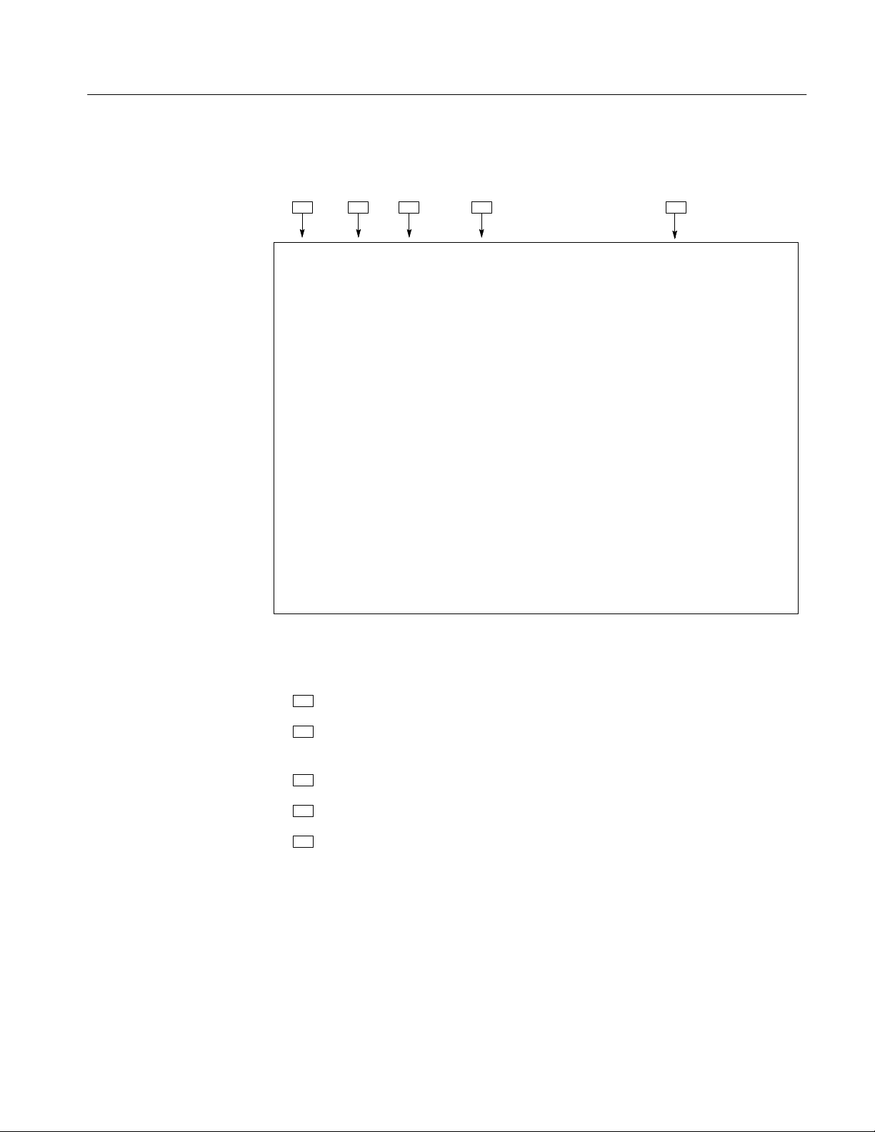
Mfr. Code to Manufacturer
Cross Index
H Instrument modification number, if applicable
If you order a part that has been replaced with a different or improved part, your
local Tektronix field office or representative will contact you concerning any
change in part number.
Abbreviations conform to American National Standard ANSI Y1.1–1972.
The table titled Manufacturers Cross Index shows codes, names, and addresses
of manufacturers or vendors of components listed in the parts list.
TMS 560 MPC860 Microprocessor Support Instruction Manual
4–1
Page 52

Replaceable Parts
Manufacturers cross index
Mfr.
code
80009 TEKTRONIX INC 14150 SW KARL BRAUN DR
Manufacturer Address City , state, zip code
PO BOX 500
Replaceable parts list
Fig. &
index
number
Tektronix
part number
070–9803–00 1 MANUAL, TECH: INSTRUTION, MICROPROCESSOR
071–0071–01 1 MANUAL, TECH: INSTRUCTIONS, MPC860,
070–9802–00 1 MANUAL, TECH: BASIC OPS MICRO SUP ON
Serial no.
effective
Serial no.
discont’d
Qty Name & description Mfr. code Mfr. part number
SUPPORT, PKG INSTALLATION, TLA700 SERIES,
LOGIC ANALYZER
TMS560, DP
OPTIONAL ACCESSORIES
DAS/TLA 500 SERIES LOGIC ANALYZERS
BEAVERT ON, OR 97077–0001
80009 070–9803–00
80009 071–0071–01
80009 070–9802–00
4–2
TMS 560 MPC860 Microprocessor Support Instruction Manual
Page 53

Index
Page 54

Page 55

Index
Numbers
16-bit area high bound, MPC specific field, 2–10
16-bit area low bound, MPC specific field, 2–10
32-bit area high bound, MPC specific field, 2–10
32-bit area low bound, MPC specific field, 2–9
8-bit area high bound, MPC specific field, 2–10
8-bit area low bound, MPC specific field, 2–10
A
about this manual set, vii
acquiring data, 2–5
Address group
channel assignments, 1–4
display column, 2–7
Alternate Bus Master Cycles, clocking option, 2–1
application, logic analyzer configuration, 1–1
B
basic operations, where to find information, vii
Big Endian, 2–9
bus cycles, displayed cycle types, 2–6
bus timing, 2–2
byte ordering, MPC specific field, 2–9
how data is acquired, 2–2
internal arbiter, 2–3
disabled, 2–3
enabled, 2–3
memory , 2–3
DRAM, 2–3
non DRAM, 2–3
memory controller, 2–3
non UPM, 2–3
UPM, 2–3
retry, 2–3
activated, 2–3
inactivated, 2–3
Show Cycles, 2–1
connections, CPU to Mictor, 1–8
contacting T ektronix, viii
Control Flow display format, 2–8
Control group
channel assignments, 1–7
symbol table, 2–3
CPM related information, functionality not supported,
1–3
CPU to Mictor connections, 1–8
Custom clocking
Alternate Bus Master Cycles, 2–1
how data is acquired, 2–2
Show Cycles, 2–1
cycle types, 2–6
C
channel asignments, 1–4
channel assignment conventions, 1–4
channel assignments
Address group, 1–4
clocks, 1–8
Control group, 1–7
Data group, 1–6
Misc group, 1–7
T siz group, 1–7
channel groups, 2–1
visibility , 2–5
clock channel assignments, 1–8
clock rate, 1–2
clocking, Custom, how data is acquired, 2–2
clocking options
alternate bus master, 2–2
excluded, 2–2
included, 2–2
Alternate Bus Master Cycles, 2–1
TMS 560 MPC860 Microprocessor Support Instruction Manual
D
data
acquiring, 2–5
disassembly formats
Control Flow, 2–8
Hardware, 2–6
Software, 2–7
Subroutine, 2–8
data cache, 1–2
data display , changing, 2–8
Data group
channel assignments, 1–6
display column, 2–7
definitions
disassembler, vii
HI module, viii
information on basic operations, vii
LO module, viii
logic analyzer, viii
Index–1
Page 56

Index
module, viii
P54C, vii
SUT, vii
XXX, vii
disassembled data
cycle type definitions, 2–6
viewing, 2–5
disassembler
definition, vii
logic analyzer configuration, 1–1
setup, 2–1
Disassembly Format Definition overlay, 2–11
Disassembly property page, 2–11
display formats
Control Flow, 2–8
Hardware, 2–6
Software, 2–7
special characters, 2–5
Subroutine, 2–8
E
electrical specifications, 3–1
exception prefix, MPC specific field, 2–9
F
functionality not supported, 1–3
CPM related information, 1–3
interrupt signals, 1–3
Show Cycle, 1–3
H
Hardware display format, 2–6
cycle type definitions, 2–6
HI module, definition, viii
logic analyzer
configuration for disassembler, 1–1
configuration for the application, 1–1
with a DAS 9200 series, 1–1
with a TLA 700 series, 1–1
definition, viii
software compatibility, 1–1
M
manual
conventions, vii
how to use the set, vii
Mark Cycle function, 2–12
Mark Opcode function, 2–12
marking cycles, definition of, 2–12
mass termination interface probes, (MTIF), 1–3
microprocessor, specific clocking and how data is
acquired, 2–2
Mictor to CPU connections, 1–8
Misc group, channel assignments, 1–7
Mnemonics display column, 2–7
module, definition, viii
MPC860 specific fields, 2–9
16-bit area high bound, 2–10
16-bit area low bound, 2–10
32-bit area high bound, 2–10
32-bit area low bound, 2–9
8-bit area high bound, 2–10
8-bit area low bound, 2–10
byte ordering, 2–9
exception prefix, 2–9
internal arbiter, 2–9
retry, 2–9
MTIF probes, 1–3
P
I
instruction cache, 1–2
internal arbiter, MPC specific field, 2–9
interrupt signals, functionality not supported, 1–3
L
labeling the P6434 probes, 1–3
Little Endian, 2–9
LO module, definition, viii
Index–2
P54C, definition, vii
P6434 probes, labeling, 1–3
PPC Little Endian, 2–9
programming the UPMs, 1–2
R
Reset, SUT hardware, 1–1
restrictions, 1–1
retry, MPC specific field, 2–9
TMS 560 MPC860 Microprocessor Support Instruction Manual
Page 57

Index
S
setups
disassembler, 2–1
support, 2–1
Show Cycle, functionality not supported, 1–3
Show Cycles, clocking option, 2–1
signals, active low sign, viii
Software display format, 2–7
special bus modes, 2–6
special characters displayed, 2–5
specifications, 3–1
electrical, 3–1
Subroutine display format, 2–8
support, setup, 2–1
support setup, 2–1
SUT, definition, vii
SUT hardware Reset, 1–1
symbol table
Control channel group, 2–3
T siz channel group, 2–3
system clock rate, 1–2
T
T ektronix, how to contact, viii
terminology, vii
T siz group
channel assignments, 1–7
display column, 2–7
symbol table, 2–3
U
UPM, programming, 1–2
V
viewing disassembled data, 2–5
X
XXX, definition, vii
TMS 560 MPC860 Microprocessor Support Instruction Manual
Index–3
Page 58

Index
Index–4
TMS 560 MPC860 Microprocessor Support Instruction Manual
 Loading...