

Page 1

Instruction Manual
TMS546
MPC7XX/MPC74XX Microprocessor
Software Support
071-1012-01
www.tektronix.com
Page 2

Copyright © Tektronix, Inc. All rights reserved.
Tektronix products are covered by U.S. and foreign patents, issued and pending. Information in this publication supercedes
that in all previously published material. Specifications and price c hange privileges reserved.
Tektronix, Inc., P.O. Box 500, Bea verton, OR 97077
TEKTRONIX and TEK are registered trademarks of Tektronix, Inc.
Page 3

SOFTWARE WARRANTY
Tektronix warrants that the media on which this software product is furnished and the encoding of the programs on
the media will be free from defects in materials and workmanship for a period of three (3) months from the date of
shipment. If a medium or encoding proves defective during the warranty period, Tektronix will provide a
replacement in exchange for the defective medium. Except as to the media on which this software product is
furnished, this software product is provided “as is” without warranty of any kind, either e xpress or implied.
Tektronix does not warrant that the func tions contained in this software product will meet Customer’s
requirements or that the operation of the programs will be uninterrupted or error-free.
In order to obtain service under this warranty, Customer must notify Tektronix of the defect before the expiration
of the warranty period. If Tektronix is unable to provide a replacement that is free from defects in materials and
workmanship within a reasonable time thereafter, Customer may terminate the license for this software product
and return this software product and any associated materials for credit or refund.
THIS WARRANTY IS GIVEN BY TEKTRONIX IN LIEU OF ANY OTHER WARRANTIES, EXPRESS
OR IMPLIED. TEKTRONIX AND ITS VENDORS DISCLAIM ANY IMPLIED WARRANTIES OF
MERCHANTABILITY OR FITNESS FOR A PARTICULAR PURPOSE. TEKTRONIX’
RESPONSIBILITY TO REPLACE DEFECTIVE MEDIA OR REFUND CUSTOMER’S PAYMENT IS
THE SOLE AND EXCLUSIVE REMEDY PROVIDED TO THE CUSTOMER FOR BREACH OF THIS
WARRANTY. TEKTRONIX AND ITS VENDORS WILL NOT BE LIABLE FOR ANY INDIRECT,
SPECIAL, INCIDENTAL, OR CONSEQUENTIAL DAMAGES IRRESPECTIVE OF WHETHER
TEKTRONIX OR THE VENDOR HAS ADVANCE NOTICE OF THE POSSIBILITY OF SUCH
DAMAGES.
Page 4

Page 5

Table of Contents
Getting Started
Operating Basics
Preface ix...................................................
Manual Conventions ix..............................................
Contacting Tektronix x.............................................
Support Package Description 1--1.......................................
Logic Analyzer Software Compatibility 1--2..............................
Logic Analyzer Configuration 1--2......................................
Requirements and Restrict ions 1--3......................................
Timing Display Format 1--5...........................................
Functionality Not Supported 1--8.......................................
Functionality Supported but Not Tested 1--8...............................
Connecting the Logic Analyzer to a Target System 1--9.....................
Labeling P6434 Probes 1--10............................................
Setting Up the Support 2--1.....................................
Installing the Support Software 2--1.....................................
Support Package Setups 2--1...........................................
Channel Group Definitions 2--4.........................................
Clocking 2--6.......................................................
Clocking Options 2--6.............................................
Custom Cl ocking 2--6.............................................
Acquiring and Viewing Disassembled Data 2--9....................
Acquiring Data 2--9..................................................
Signal Acquisition with MPC7410 and MPC7450 Support 2--10................
60X Bus Mode Description 2--10.....................................
MPX Bus Mode Description 2--12....................................
Signal Acquisition with MPC7410_ALT and MPC7410_QD Support 2--14.......
Viewing Disassembled Data 2--14........................................
Hardware Display Format 2--15......................................
Software Display Format 2--18.......................................
Control Flow Display Format 2--19...................................
Subroutine Display Format 2--20.....................................
Changing How Data is Displayed 2--21...................................
Optional Display Selections 2--22....................................
Micro Specific Fields for MPC7410 Support 2--22.......................
Micro Specific Fields for MPC7450 Support 2--26.......................
Micro Specific Fields for MPC7410_ALT Support 2--29..................
Micro Specific Fields for MPC7410_QD Support 2--33...................
Marking Cycles 2--37..............................................
Displaying Exception Labels 2--38...................................
Viewing an Example of Disassembled Data 2--39...........................
TMS546 MPC7XX/MPC74XX Microprocessor Software Support
i
Page 6

Table of Contents
Reference
Internal Trace Reconstruction (ITR) 2--39.................................
Memory Image (S-record) 2--40......................................
Image Reader 2--40................................................
Viewing Cache Activity 2--40.......................................
Reference: Symbol and Channel Assignment Tables 3--1.............
Symbol Tables 3--1..................................................
Symbol Tables for MPC7410 Support 3--1............................
Symbol Tables for MPC7450 Support 3--4............................
Symbol Tables for MPC7410_ALT Support 3--8........................
Symbol Tables for MPC7410_QD Support 3--11.........................
Channel Assignment Tables 3--15........................................
Channel Assignment for MPC7410 3--15..............................
Channel Assignments for MPC7450 3--21..............................
Channel Assignments for MPC7410_ALT 3--28.........................
Channel Assignments for MPC7410_QD 3--36..........................
Logic Analyzer Channels not Connected for MPC7410 and
MPC7450 Support 3--44.....................................
Logic Analyzer Channels not Connected for MPC7410_QD
Support 3--45.............................................
Logic Analyzer Channels not Connected for MPC7410_ALT
Support 3--45.............................................
CPU To Mictor Connections 3--46.......................................
Connections for MPC740/750 3--46...................................
Connections for MPC745/755 3--52...................................
Connections for MPC7400 3--57.....................................
Connections for MPC7410 3--62.....................................
Connections for MPC7450 3--67.....................................
Connections for PPC750CX 3--72....................................
Connections for MPC7410_ALT Support 3--77..........................
Connections for MPC7410_QD Support 3--83...........................
Specifications
Replaceable Parts List
Index
ii
Specification Tables 4--1..............................................
I/O Voltage Level Difference for MPC7XX processors and MPC74XX
processors 4--1..................................................
Parts Ordering Information 5 --1.........................................
Using the Replaceable Parts List 5--1....................................
TMS546 MPC7XX/MPC74XX Microprocessor Software Support
Page 7

List of Figures
Table of Contents
Figure 2--1: 60X bus timing diagram 2--10..........................
Figure 2--2: Example of Hardware display format 2--18...............
Figure 2--3: Example of Software display format 2--19................
Figure 2--4: Example of Control Flow display format 2--20............
Figure 2--5: Example of Subroutine display format 2--21..............
Figure 2--6: Example of Property Page 2--43........................
Figure 2--7: Display showing Fetch Stream 2--44.....................
Figure 2--8: Display showing Memory Image 2--45...................
TMS546 MPC7XX/MPC74XX Microprocessor Software Support
iii
Page 8

Table of Contents
List of Tables
Table 2--1: MPC7410 group names 2--4...........................
Table 2--2: MPC7450 group names 2--5..........................
Table 2--3: MPC7410_ALT group names 2--5.....................
Table 2--4: MPC7410_QD group names 2--6......................
Table 2--5: Sample points in 60X bus-mode 2--11....................
Table 2--6: Signal acquisition for MPC7410 60X bus mode 2--11.......
Table 2--7: Sample points in MPX bus mode 2--12...................
Table 2--8: Signal acquisition for MPC7410 MPX bus mode 2--13......
T able 2--9: Description of special characters in the display 2--14.......
Table 2--10: Cycle type labels for Address sequences and
definitions 2--15............................................
Table 2--11: Cycle type labels for Data sequences and definitions 2--16..
Table 2--12: General cycle type labels definitions 2--17...............
Table 2--13: Logic analyzer disassembly display options 2--22.........
T able 2--14: Mark selections and definitions 2--38...................
Table 2--15: Interrupt and exception labels 2--38....................
Table 3--1: MPC7410_Control group symbol table definitions 3--1....
Table 3--2: MPC7410_Transfer group symbol table definitions 3--2...
Table 3--3: MPC7410_T_Size group symbol table definitions 3--4.....
Table 3--4: MPC7450_Control group symbol table definitions 3--4....
Table 3--5: MPC7450_Transfer group symbol table definitions 3--6...
Table 3--6: MPC7450_T_Size group symbol table definitions 3--7.....
Table 3--7: MPC7410_ALT_Control group symbol table
definitions 3--8............................................
Table 3--8: MPC7410_ALT_Transfer group symbol table
definitions 3--9............................................
Table 3--9: MPC7410_ALT_T_Size group symbol table
definitions 3--10............................................
Table 3--10: MPC7410_QD_Control group symbol table
definitions 3--11............................................
Table 3--11: MPC7410_QD_Transfer group symbol table
definitions 3--12............................................
Table 3--12: MPC7410_QD_T_Size group symbol table
definitions 3--14............................................
Table 3--13: Address group channel assignments for MPC7410 3--15...
iv
TMS546 MPC7XX/MPC74XX Microprocessor Software Support
Page 9

Table of Contents
Table 3--14: High_Data group channel assignments for
MPC7410 3--16.............................................
Table 3--15: Low_Data group channel assignments for
MPC7410 3--17.............................................
Table 3--16: Control group channel assignments for MPC7410 3--19....
Table 3--17: Transfer group channel assignments for MPC7410 3--19...
Table 3--18: T_Size group channel assignments for MPC7410 3--20....
Table 3--19: Misc group channel assignments for MPC7410 3--20......
Table 3--20: DTI group channel assignments for MPC7410 3--21.......
Table 3--21: MSB_Addr group channel assignments for
MPC7450 3--21.............................................
Table 3--22: Address group channel assignments for
MPC7450 3--21.............................................
Table 3--23: Low_Data group channel assignments for
MPC7450 3--23.............................................
Table 3--24: High_Data group channel assignments for
MPC7450 3--24.............................................
Table 3--25: Control group channel assignments for MPC7450 3--25....
Table 3--26: Transfer group channel assignments for MPC7450 3--26...
Table 3--27: Transfer Size group assignments for MPC7450 3--27......
Table 3--28: Misc group assignments for MPC7450 3--27.............
Table 3--29: DTI group assignments for MPC7450 3--28..............
Table 3--30: Address group channel assignments for
MPC7410_ALT 3--28........................................
Table 3--31: High_Data group channel assignments for
MPC7410_ALT 3--29........................................
Table 3--32: Low_Data group channel assignments for
MPC7410_ALT 3--31........................................
Table 3--33: Control group channel assignments for
MPC7410_ALT 3--32........................................
Table 3--34: Transfer group channel assignments for
MPC7410_ALT 3--33........................................
Table 3--35: Transfer Size group assignments for
MPC7410_ALT 3--33........................................
Table 3--36: ODT group assignments for MPC7410_ALT 3--34........
Table 3--37: P0_Signals group assignments for MPC7410_ALT 3--34...
Table 3--38: P1_Signals group assignments for MPC7410_ALT 3--35...
Table 3--39: Misc group assignments for MPC7410_ALT 3--35........
Table 3--40: Address group channel assignments for
MPC7410_QD 3--36.........................................
TMS546 MPC7XX/MPC74XX Microprocessor Software Support
v
Page 10

Table of Contents
Table 3--41: High_Data group channel assignments for
MPC7410_QD 3--37.........................................
Table 3--42: Low_Data group channel assignments for
MPC7410_QD 3--38.........................................
Table 3--43: Control group channel assignments for
MPC7410_QD 3--40.........................................
Table 3--44: Transfer group channel assignments for
MPC7410_QD 3--41.........................................
Table 3--45: Transfer Size group assignments for
MPC7410_QD 3--41.........................................
Table 3--46: ODT group assignments for MPC7410_QD 3--42.........
Table 3--47: P0_Signals group assignments for MPC7410_QD 3--42....
Table 3--48: P1_Signals group assignments for MPC7410_QD 3--43....
Table 3--49: P2_Signals group assignments for MPC7410_QD 3--43....
Table 3--50: P3_Signals group assignments for MPC7410_QD 3--44....
Table 3--51: Misc group assignments for MPC7410_QD 3--44.........
Table 3--52: Clock channel assignments 3--45.......................
Table 3--53: Recommended pin assignments for a Mictor connector
(component side) 3--46.......................................
Table 3--54: CPU to Mictor connections for Mictor A pins for
MPC740/750 3--46..........................................
Table 3--55: CPU to Mictor connections for Mictor C pins for
MPC740/750 3--48..........................................
Table 3--56: CPU to Mictor connections for Mictor D pins for
MPC740/750 3--49..........................................
Table 3--57: CPU to Mictor connections for Mictor E pins for
MPC740/750 3--50..........................................
Table 3--58: CPU to Mictor connections for Mictor A pins for
MPC745/755 3--52..........................................
Table 3--59: CPU to Mictor connections for Mictor C pins for
MPC745/755 3--53..........................................
Table 3--60: CPU to Mictor connections for Mictor D pins for
MPC745/755 3--54..........................................
Table 3--61: CPU to Mictor connections for Mictor E pins for
MPC745/755 3--55..........................................
Table 3--62: CPU to Mictor connections for Mictor A pins for
MPC7400 3--57.............................................
Table 3--63: CPU to Mictor connections for Mictor C pins for
MPC7400 3--58.............................................
Table 3--64: CPU to Mictor connections for Mictor D pins for
MPC7400 3--59.............................................
vi
TMS546 MPC7XX/MPC74XX Microprocessor Software Support
Page 11

Table 3--65: CPU to Mictor connections for Mictor E pins for
MPC7400 3--61.............................................
Table 3--66: CPU to Mictor connections for Mictor A pins for
MPC7410 3--62.............................................
Table 3--67: CPU to Mictor connections for Mictor C pins for
MPC7410 3--63.............................................
Table 3--68: CPU to Mictor connections for Mictor D pins for
MPC7410 3--65.............................................
Table 3--69: CPU to Mictor connections for Mictor E pins for
MPC7410 3--66.............................................
Table 3--70: CPU to Mictor connections for Mictor A pins for
MPC7450 3--67.............................................
Table 3--71: CPU to Mictor connections for Mictor C pins for
MPC7450 3--68.............................................
Table 3--72: CPU to Mictor connections for Mictor D pins for
MPC7450 3--70.............................................
Table 3--73: CPU to Mictor connections for Mictor E pins for
MPC7450 3--71.............................................
Table 3--74: CPU to Mictor connections for Mictor A pins for
PPC750CX 3--72...........................................
Table 3--75: CPU to Mictor connections for Mictor C pins for
PPC750CX 3--73...........................................
Table 3--76: CPU to Mictor connections for Mictor D pins for
PPC750CX 3--75...........................................
Table 3--77: CPU to Mictor connections for Mictor E pins for
PPC750CX 3--76...........................................
Table 3--78: CPU to Mictor connections for Mictor A pins for
MPC7410_ALT 3--77........................................
Table 3--79: CPU to Mictor connections for Mictor C pins for
MPC7410_ALT 3--79........................................
Table 3--80: CPU to Mictor connections for Mictor D pins for
MPC7410_ALT 3--80........................................
Table 3--81: CPU to Mictor connections for Mictor E pins for
MPC7410_ALT 3--81........................................
Table 3--82: CPU to Mictor connections for Master Module
Mictor A pins for MPC7410_QD 3--83.........................
Table 3--83: CPU to Mictor connections for Master Module
Mictor C pins for MPC7410_QD 3--84.........................
Table 3--84: CPU to Mictor connections for Master Module
Mictor D pins for MPC7410_QD 3--85.........................
Table 3--85: CPU to Mictor connections for Slave Module
Mictor D pins for MPC7410_QD 3--87.........................
Table of Contents
TMS546 MPC7XX/MPC74XX Microprocessor Software Support
vii
Page 12

Table of Contents
Table 3--86: CPU to Mictor connections for Slave Module
Mictor C pins for MPC7410_QD 3--88.........................
T able 4--1: Electrical specifications 4--1...........................
Table 4--2: I/O voltage level for MPC74XX processors 4--1...........
viii
TMS546 MPC7XX/MPC74XX Microprocessor Software Support
Page 13

Preface
This instruction manual contains specific information about the TMS546
MPC7410 microprocessor support package and is part of a set of information on
how to operate this product on compatible Tektronix logic analyzers.
If you are familiar with operating microprocessor support packages on the logic
analyzer for which the TMS546 MPC7410 support was purchased, you will
probably only need this instruction manual to set up and run the support.
If you are not familiar with operating microprocessor support packages, you will
need to supplement this instruction manual with information on basic operations
to set up and run the support.
Information on basic operations of microprocessor s upport packages is included
with each product. Each logic analyzer includes basic information that describes
how to perform tasks common to s upport packages on that platform. This
information can be in the form of logic analyzer online help, an installation
manual, or a user manual.
This manual provides detailed information on the following topics:
H Connecting the logic analyzer to the target system
Manual Conventions
H Setting up the logic analyzer to acquire data from the target system
H Acquiring and viewing disassembled data
This manual uses the following conventions:
H The term “disassembler” refers to the software that disassembles bus cycles
into instruction mnemonics and cycle types.
H The phrase “information on basic operations” refers to logic analyzer online
help or a user manual, covering the basic operations of the microprocessor
support.
H The term “logic analyzer” refers to the Tektronix logic analyzer for which
this product was purchased.
TMS546 MPC7XX/MPC74XX Microprocessor Software Support
ix
Page 14

Contacting Tektronix
Preface
Phone 1-800-833-9200*
Address Tektronix, Inc.
Department or name (if known)
14200 SW Karl Braun Drive
P.O. Box 500
Beaverton, OR 97077
USA
Web site www.tektronix.com
Sales support 1-800-833-9200, select option 1*
Service support 1-800-833-9200, select option 2*
Technical support Email: techsupport@tektronix.com
1-800-833-9200, select option 3*
6:00 a.m. -- 5:00 p.m. Pacific time
* This phone number is toll free in North America. After office hours, please leave a
voice mail message.
Outside North America, contact a Tektronix sales office or distributor; see the
Tektronix web site for a list of offices.
TMS546 MPC7XX/MPC74XX Microprocessor Software Supportx
Page 15

Getting Started
Page 16

Page 17

Getting Started
This section contains information on the TMS546 MPC7410 microprocessor
support, and information on connecting your logic analyzer to your target system.
Support Package Description
The TMS546 microprocessor support package displays disassembled data from
systems based on MPC740/745/750/755/7400/7410/7441/7445/7450/7451/7455,
PPC750FX and PPC750CX PowerPC microprocessors. The TMS546 microprocessor support package will install four supports.
H MPC7410 will support MPC740, MPC745, MPC750, MPC755, MPC7400,
MPC7441, MPC7445, MPC7410, MPC7450, MPC7451, MPC7455, and
PPC750CX, and PPC750FX PowerPCs.
H MPC7450 will support MPC7441, MPC7450, MPC7451, and MPC7455
PowerPCs.
H MPC7410_ALT will support alternate layout and dual processor disassembly
for MPC7400, MPC7410, MPC7441, MPC7445, MPC7450, MPC7451, and
MPC7455 PowerPCs.
H MPC7410_QD will support alternate layout and quad processor disassembly
for MPC7400, MPC7410, MPC7441, MPC7445, MPC7450, MPC7451, and
MPC7455 PowerPCs.
Contact your Tektronix sales representatives for a current list of supported
MPC7XX/74XX processors.
The TMS546 support package has Internal Trace Reconstruction (ITR) feature
for all processors, both in 60X and MPX bus modes.
TMS546 Compatibility. The TMS546 support package channel assignment is
compatible with the earlier Mictor pin assignment for TMS541 PPC7X0 and
TMS545 PPC7400 processor supports. If you have an
MPC7441/7445/7450/7451/7455 PowerPC board with a TMS541 or TMS545
channel assignment, you get correct disassembly (except for control symbol
tables) by loading MPC7410 support and selecting the MPC7450 processor to
disassemble.
TMS546 MPC7XX/MPC74XX Microprocessor Software Support
1--1
Page 18

Getting Started
NOTE. Refer to TMS541 and TMS545 Microprocessor Support Instruction
Manuals if your MPC7450 board has TMS541 and TMS545 channel assignments.
Refer to information on basic operations to determine how many modules and
probes your logic analyzer needs to meet the minimum channel requirements for
the TMS546 microprocessor support.
To use this support efficiently, you need the items listed in the information on
basic operations in your logic analyzer online help and the following user
manuals.
H MPC7450 RISC Microprocessor Family User Manual {Motorola, 12/2001,
and Rev 2, MPC7450UM/D}
H PPC750CX RISC Microprocessor User Manual {IBM, 10/2000 and Rev 1.1)
H MPC7410 RISC Microprocessor User Manual {Motorola, 10/2000, and
Rev 0, MPC7410UM/D}
H MPC7400 RISC Microprocessor User Manual {Motorola, 3/2000, and
Rev 0, MPC7400UM/D}
H MPC750 RISC Microprocessor User Manual {Motorola, 8/1997, and
MPC750UM/AD}
H MPC755 RISC Microprocessor User Manual {Motorola, 10/2000, and
Rev 0.1, MPC755UM/D}
H Outstanding Data Tenures on the MPX Bus AN2161/d from Motorola.
Logic Analyzer Software Compatibility
The label on the microprocessor support floppy disk states which version of logic
analyzer software this support is compatible with.
Logic Analyzer Configuration
The TMS546 MPC7410 support allows a choice of required minimum module
configurations:
H MPC7410 support requires a minimum of one 136 channel, 200 MHz
module
1--2
H MPC7450 support requires a minimum of one 136 channel, 200 MHz
module
TMS546 MPC7XX/MPC74XX Microprocessor Software Support
Page 19

Getting Started
H MPC7410_ALT support requires a minimum of one 136 channel 200 MHz
module
H MPC7410_QD support requires a minimum of two 102 channel 200 MHz
modules in merged configuration
Requirements and Restrictions
Review electrical specifications in the Specifications section in this manual as
they pertain to your target system, as well as the following descriptions of other
TMS546 MPC7410 support requirements and restrictions.
If the board has the recommended TMS546 MPC7410 support channel assignment, then load MPC7410 support to disassemble the
MPC740/745/750/755/7400/7441/7445/7410/7450/7451/7455/PPC750CX/
PPC750FX processors.
If the board has the recommended TMS546 MPC7450 support channel assignment, then load MPC7450 support to disassemble the
MPC7450/7451/7455/7441/7445 processors.
If the board has recommended TMS546 MPC7410_ALT support channel
assignment, then load the MPC7410_ALT support to disassemble the
MPC7441/7445/7450/7451/7455 processors.
If the board has recommended TMS546 MPC7410_QD support channel
assignment, then load the MPC7410_QD support to disassemble the
MPC7441/7445/7450/7451/7455 processors.
Hardware Reset. If a hardware reset occurs in your TMS546 MPC7410 system
during an acquisition, the application disassembler might acquire an invalid
sample.
System Clock Rate(SYSCLK). The TMS546 MPC7410 microprocessor support can
acquire data from the TMS546 MPC7410 microprocessor operating at speeds of
upto 166 MHz
1
. The TMS546 MPC7410 microprocessor support has been tested
to 100 MHz.
Address Pipeline. The TMS546 support package is designed to support upto
16-level address pipelining. While acquiring data from systems having pipelining, the acquisition may have data tenures without any corresponding address
tenures at the beginning of the acquisition. The disassembler, by default, starts
associating the first acquired data tenure with the first acquired address tenure.
This may cause wrong disassembly. You have to associate the first acquired
1
Specification at time of printing. Contact your Tektronix sales representative for
current information on the fastest devices supported.
TMS546 MPC7XX/MPC74XX Microprocessor Software Support
1--3
Page 20

Getting Started
address tenure with the correct data tenure. This is done using “Invalid data”
marking option. You must mark all the data tenures without any corresponding
address as “Invalid data”. Once you associate a address tenure with the correct
data tenure, the disassembly adjusts itself for the change in the pipeline depth.
Setup and Hold Time Adjustments. You cannot change the setup and hold time for
any signal group.
HID0[IFTT] Bit Setting for TMS546 Support. When using TMS546 support for
MPC7400 and MPC7410 PowerPC the HID0[IFTT] must be set to 1 for a perfect
read/fetch indication. In this case, the disassembly uses TT signals for labeling
the cycles as Read or Fetch. If you do not set this bit, the disassembly uses
heuristic method to decide between Read and Fetch cycles.
Nonintrusive Acquisition. Acquiring microprocessor bus cycles is nonintrusive to
the target system. That is, the TMS546 MPC7410 does not intercept, modify, or
present signals back to the target system.
Channel Groups. Channel groups required for clocking and disassembly for
TMS546 MPC7410 microprocessor support are as follows:
MPC7410:
Address Group, High_Data Group, Low_Data Group, Control Group, Transfer
Group, T_Size Group, DTI Group and Misc Group.
MPC7450:
MSB_Addr Group, Address Group, High_Data Group, Low_Data Group,
Transfer Group, T_Size Group, Control Group, DTI Group and Misc Group.
MPC7410_ALT:
Address Group, High_Data Group, Low_Data Group, TraceAddr Group,
Transfer Group, T_Size Group, Control Group, ODT Group, P0_Signals Group,
P1_Signals Group, and Misc Group.
MPC7410_QD:
Address Group, High_Data Group, Low_Data Group, TraceAddr Group,
Transfer Group, T_Size Group, Control Group, ODT Group, P0_Signals Group,
P1_Signals Group, P2_Signals Group, P3_Signals Group, and Misc Group.
Disabling the Instruction and Data Cache. Disabling the instruction cache makes
all instruction prefetches visible on the bus so that they can be acquired and
displayed disassembled.
1--4
Disabling the data cache makes visible on the bus all the loads and stores to
memory, including data reads and writes, so that the software can acquire and
TMS546 MPC7XX/MPC74XX Microprocessor Software Support
Page 21

Getting Started
Timing Display Format
display them. To view the cache activity, Internal Trace Reconstruction (ITR)
feature of the support must be enabled.
Viewing Instruction Cache Activity. To view the instruction cache activity, set the
disassembly option “Disassemble based on” to Memory Image. For further
details, see the section Viewing Cache Activity on page 2--40.
Memory Image Mode. In Memory Image Mode, Non-Memory Image (or Fetch
Stream) cycles are displayed.
Fetches/Reads as Read label corresponding to Transfer Type
Writes as Write label corresponding to Transfer Type
A Timing Display Format file is also provided for this support. It sets up the
display to show the following waveforms for the TMS546 microprocessor
support.
For MPC7410:
SYSCLK
Address
High_Data
Low_Data
BR_
BG_
TS_
ABB_
AMON_
AACK_
ARTRY_
TBST_
DBB_
DMON_
DBG_
TA_
TEA_
DRTRY_/DTI[1]
Control
T_Size
Transfer
DTI
Misc
TMS546 MPC7XX/MPC74XX Microprocessor Software Support
1--5
Page 22

Getting Started
NOTE. Address, High_Data, Low_Data, Control, T_Size, Transfer, DTI, and Misc
groups are in busform.
For MPC7450:
SYSCLK
MSB_Addr
Address
High_Data
Low_Data
BR_
BG_
TS_
AMON_
AACK_
ARTRY_
TBST_
DMON_
DBG_
TA_
TEA_
Control
T_Size
Transfer
DTI
Misc
1--6
NOTE. MSB_Addr, Address, High_Data, Low_Data, Control, T_Size, Transfer,
DTI, and Misc groups are in busform.
For MPC7410_ALT:
SYSCLK
Address
High_Data
Low_Data
Transfer
T_Size
P0_DRDY_
P0_BG_
P1_DRDY_
TS_
TBST_
P1_BG_
P0_HIT_
AACK_
ARTRY_
TMS546 MPC7XX/MPC74XX Microprocessor Software Support
Page 23

Getting Started
P0_DBG_
P0_DTI0/DBWO_
P1_HIT_
TA_
TEA_
P1_DTI0/DBWO_
P1_DBG_
P0_Signals
P1_Signals
ODT
NOTE. Address, High_Data, Low_Data, Transfer, T_Size, P0_Signals, P1_Signals, and ODT groups are displayed in busform.
For MPC7410_QD:
Sample
SYSCLK
Address
High_Data
Low_Data
Transfer
T_Size
P0_Signals
P1_Signals
P2_Signals
P3_Signals
ODT
P3_DRDY_
P3_BG_
P3_DBG_
P3_DTI0/DBWO_
P3_HIT_
P2_DRDY_
P2_BG_
P2_DBG_
P2_DTI0/DBWO_
P2_HIT_
P0_DRDY_
P0_BG_
P1_DRDY_
TS_
TBST_
P1_BG_
WT_
P0_HIT_
AACK_
TMS546 MPC7XX/MPC74XX Microprocessor Software Support
1--7
Page 24

ARTRY_
P0_DBG_
P0_DTI0/DBWO_
P1_HIT_
TA_
TEA_
P1_DTI0/DBWO_
P1_DBG_
NOTE. Address, High_Data, Low_Data, Transfer, T_Size, P0_Signals, P1_Signals, and ODT groups are displayed in busform.
The method of selecting or restoring the Timing Display Format file is different
for each platform, and is ignored in this document.
Functionality Not Supported
Getting Started
L2 Cache. L2 cache transactions are not supported by the TMS546 support
package.
Extended Addressing Mode. Extended addressing mode is not supported by the
TMS546 support package, except in the MPC7450 support.
Functionality Supported but Not Tested
The TMS546 support package supports these functionalities but they are not
tested completely:
H 32-bit data bus mode with MPC7X5 processors.
H Disassembly is not tested for MPC740, MPC745, MPC7441, MPC7445,
MPC7451, PPC750CX, and PPC750FX PowerPCs.
H MPX bus mode with 74XX processors is not tested for the non-zero value of
of the DTI group.
NOTE. For latest information on MPX support contact your local Tektronix field
office or representative.
1--8
TMS546 MPC7XX/MPC74XX Microprocessor Software Support
Page 25

Getting Started
H Alternate master disassembly is partially tested.
H Disassembly tested for one-level address pipeline but designed to support
16-level pipeline.
Connecting the Logic Analyzer to a Target System
You can use the channel probes, clock probes, and leadsets with a commercial
test clip (or adapter) to make the connections between the logic analyzer and
your target system.
To connect the probes to TMS546 MPC7410 signals in the target system using a
test clip, follow the steps:
1. Power off your target system. It is not necessary to power off the logic
analyzer.
CAUTION. To prevent static damage, handle the microprocessor, probes, and the
logic analyzer module in a static-free environment. Static discharge can damage
these components.
Always wear a grounding wrist strap, heel strap, or similar device while
handling the microprocessor.
2. To discharge your stored static electricity, touch the ground connector located
on the back of the logic analyzer. If you are using a test clip, touch any of the
ground pins on the clip to discharge stored electricity from the test clip.
CAUTION. To prevent permanent damage to the pins on the microprocessor, place
the target system on a horizontal surface before connecting the test clip.
3. Place the target system on a horizontal, static-free surface.
4. Use Tables 3--13 through 3--52 starting on page 3--15 to connect the channel
probes to TMS546 MPC7410 signal pins on the test clip or in the target
system.
5. Use leadsets to connect at least one ground lead from each channel and the
ground lead from each clock probe to the ground pins on your test clip.
TMS546 MPC7XX/MPC74XX Microprocessor Software Support
1--9
Page 26

Labeling P6434 Probes
Getting Started
The TMS546 hardware support package relies on the channel mapping and
labeling scheme for the P6434 Probes. Apply labels using the instructions
described in the P6434 Probe Instructions manual.
1--10
TMS546 MPC7XX/MPC74XX Microprocessor Software Support
Page 27

Operating Basics
Page 28

Page 29

Setting Up the Support
This section provides information on how to set up the support and covers the
following topics:
H Channel group definitions
H Clocking options
The information in this section is specific to the operations and functions of the
TMS546 MPC7410 support on any Tektronix logic analyzer for which the
support can be purchased. Information on basic operations describes general
tasks and functions.
Before you acquire and display disassembled data, you need to load the support
and specify the setups for clocking and triggering as described in the information
on basic operations. The support provides default values for each of these setups,
but you can change them as needed.
Installing the Support Software
NOTE. Before you install any software, it is recommended you verify the
microprocessor support software is compatible with the logic analyzer software.
To install the TMS546 MPC7410 software on your Tektronix logic analyzer,
follow these steps:
1. Insert the floppy disk in the disk drive.
2. Click the Windows Start button, point to Settings, and click Control Panel.
3. In the Control Panel window, double-click Add/Remove Programs.
4. Follow the instructions on the screen for installing the software from the
To remove or uninstall software, follow the above instructions and select
Uninstall. You need to close all windows before you uninstall any software.
Support Package Setups
The TMS546 MPC7410 software installs four support packages. Each support
package offers different clocking and display options.
floppy disk.
TMS546 MPC7XX/MPC74XX Microprocessor Software Support
2--1
Page 30

Setting Up the Support
Acquisition Setup The TMS546 MPC7410 affects the logic analyzer setup menus
(and submenus) by modifying existing fields and adding micro-specific fields.
On the logic analyzer, the TMS546 MPC7410 adds the selection “MPC7410”,
“MPC7450”, “MPC7410_ALT”,and“MPC7410_QD” to the Load Support
Package dialog box, under the File pulldown menu. Once the “TMS546
MPC7410” support is loaded, the “Custom” clocking mode selection in the logic
analyzer Module Setup menu is also enabled.
MPC7410 Setup. This setup provides disassembly support for the
MPC740/750/745/755/7400/7410/7441/7445/7450/7451/7455, PPC750CX, and
PPC750FX PowerPC processors.
Disassembly channel groups:
Sample
Address
High_Data
Low_Data
TraceAddr
Mnemonics
Timestamp
Timing channel groups:
Sample
Address
High_Data
Low_Data
Transfer
T_Size
Control
DTI
Misc
MPC7450 Setup. MPC7450 setup provides disassembly support for the
MPC7441/7445/7450/7451/7455 PowerPC processors.
Disassembly channel groups:
Sample
MSB_Addr
Address
High_Data
Low_Data
TraceAddr
Mnemonics
Timestamp
2--2
TMS546 MPC7XX/MPC74XX Microprocessor Software Support
Page 31

Setting Up the Support
Timing channel groups:
Sample
Address
High_Data
Low_Data
Transfer
T_Size
Control
DTI
Misc
MPC7410_ALT Setup. The MPC7410_ALT setup provides disassembly support for
the MPC7400/7410/7441/7445/7450/7451/7455 PowerPC processors.
Disassembly channel groups:
Sample
Address
High_Data
Low_Data
TraceAddr
Mnemonics
Timestamp
Timing channel groups:
Sample
Address
High_Data
Low_Data
Transfer
T_Size
Control
P0_Signals
P1_Signals
ODT
Misc
MPC7410_QD Setup. The MPC7410_QD setup provides disassembly support for
the MPC7400/7410/7441/7445/7450/7451/7455 PowerPC processors.
Disassembly channel groups:
Sample
Address
High_Data
Low_Data
TMS546 MPC7XX/MPC74XX Microprocessor Software Support
2-- 3
Page 32

Setting Up the Support
TraceAddr
Mnemonics
Timestamp
Timing channel groups:
Sample
Address
High_Data
Low_Data
Transfer
T_Size
Control
P0_Signals
P1_Signals
P2_Signals
P3_Signals
ODT
Misc
Channel Group Definitions
The software automatically defines channel groups for the support. The channel
groups for the TMS546 MPC7410 support for MPC7410 are Address,
High_Data, Low_Data, Control, T_Size, Transfer, DTI, and Misc.
Table 2--1: MPC7410 group names
Group name Display radix
Address HEX
High_Data HEX
Low_Data HEX
TraceAddr HEX
Mnemonic NONE (Disassembly generated text)
Transfer SYM (default OFF)
T_Size SYM (default OFF)
Control SYM (default OFF)
DTI HEX (default OFF)
Misc HEX (default OFF)
2-- 4
TMS546 MPC7XX/MPC74XX Microprocessor Software Support
Page 33

Setting Up the Support
The channel groups for MPC7450 support are MSB_Addr, Address, High_Data,
Low_Data, Control, T_Size, Transfer, DTI, and Misc.
Table 2--2: MPC7450 group names
Group name Display radix
MSB_Addr HEX
Address HEX
High_Data HEX
Low_Data HEX
TraceAddr HEX
Mnemonic NONE (Disassembly generated text)
Transfer SYM (default OFF)
T_Size SYM (default OFF)
Control SYM (default OFF)
DTI HEX (default OFF)
Misc HEX (default OFF)
The channel groups for MPC7410_ALT support are Address, High_Data,
Low_Data, TraceAddr, Control, T_Size, Transfer, ODT, P0_Signals, P1_Signals,
and Misc.
Table 2--3: MPC7410_ALT group names
Group name Display radix
Address HEX
High_Data HEX
Low_Data HEX
TraceAddr HEX
Mnemonic NONE (Disassembly generated text)
Transfer SYM (default OFF)
T_Size SYM (default OFF)
Control SYM (default OFF)
P0_Signals HEX (default OFF)
P1_Signals HEX (default OFF)
ODT HEX (default OFF)
Misc HEX (default OFF)
TMS546 MPC7XX/MPC74XX Microprocessor Software Support
2-- 5
Page 34

Setting Up the Support
The channel groups for MPC7410_QD support are Address, High_Data,
Low_Data, TraceAddr, Control, T_Size, Transfer, ODT, P0_Signals, P1_Signals,
P2_Signals, P3_Signals, and Misc.
Table 2--4: MPC7410_QD group names
Group name Display radix
Address HEX
High_Data HEX
Low_Data HEX
TraceAddr HEX
Mnemonic NONE (Disassembly generated text)
Transfer SYM (default OFF)
T_Size SYM (default OFF)
Control SYM (default OFF)
P0_Signals HEX (default OFF)
P1_Signals HEX (default OFF)
P2_Signals HEX (default OFF)
P3_Signals HEX (default OFF)
ODT HEX (default OFF)
Misc HEX (default OFF)
Clocking
Clocking Options
Custom Clocking
If you want to know which signal is in which group, refer to the channel
assignment tables beginning on page 3--15.
The TMS546 support offers a microprocessor-specific clocking mode for the
TMS546 MPC7410 microprocessor. This clocking mode is the default selection
whenever you load the MPC7410, MPC7450, MPC7410_ALT, or MPC7410_QD
supports.
Disassembly is not correct with the Internal or External clocking modes.
Information on basic operations describes how to use these clock selections for
general purpose analysis.
A special clocking program is loaded to the module every time you load the
MPC7410, MPC7450, MPC7410_ALT, or MPC7410_QD supports. This special
clocking is called Custom.
2-- 6
TMS546 MPC7XX/MPC74XX Microprocessor Software Support
Page 35

Setting Up the Support
With Custom clocking, the module logs in signals from multiple channel groups
at different times when the signals are valid on the TMS546 MPC7410 bus. The
module then sends all the logged-in signals to the trigger machine and to the
acquisition memory of the module for storage.
For MPC7410 and MPC7450 Supports. In Custom clocking, the module clocking
state machine (CSM) generates one master sample for each microprocessor bus
cycle, no matter how many clock cycles are contained in the bus cycle.
When Custom Clocking is selected, the Custom Clocking options menu has the
subtitle MPC7410 or MPC7450 Microprocessor Clocking Support added, and
displays the clocking option “PowerPC Clocking Mode”, that allows you to
select the following options for both the supports:
60X . Select the 60X bus mode operation for the PowerPCs (default).
MPX. Select the MPX bus mode operation for the PowerPCs.
For MPC7410_ALT and MPC7410_QD Supports. In custom clocking, the module
clocking state machine (CSM) generates one master sample for every rising edge
of the system clock.
The custom clocking option is always set to “Default”.
TMS546 MPC7XX/MPC74XX Microprocessor Software Support
2-- 7
Page 36

Setting Up the Support
2-- 8
TMS546 MPC7XX/MPC74XX Microprocessor Software Support
Page 37

Acquiring and Viewing Disassembled Data
This section describes how to acquire data and view it disassembled. The
following information covers these topics and tasks:
H Acquiring data
H Viewing disassembled data in various display formats
H Viewing cycle type labels
H Changing the way data is displayed
H Changing disassembled cycles with the mark cycles function
Acquiring Data
The TMS546 MPC7410 software package installs software support for the
following processors.
H MPC7410 support: MPC740, MPC745, MPC750, MPC755, MPC7400,
MPC7410, MPC7441, MPC7445, MPC7450, MPC7451, MPC7455,
PPC750CX, and PPC750FX processors.
H MPC7450 support: MPC7441, MPC7445, MPC7450, MPC7451, and
MPC7455 processors.
H MPC7410_ALT support: MPC7400, MPC7410, MPC7441, MPC7445,
MPC7450, MPC7451, and MPC7455 processors.
H MPC7410_QD support: MPC7400, MPC7410, MPC7441, MPC7445,
MPC7450, MPC7451, and MPC7455 processors.
The TMS546 support has Internal Trace Reconstruction (ITR) feature for all
processors, both in 60X and MPX bus mode, for all the supports.
Once you load MPC7410, MPC7450, MPC7410_ALT or MPC7410_QD support
packages, choose a clocking mode, and specify the trigger, you are ready to
acquire and disassemble data.
If you have any problems acquiring data, refer to information on basic operations
in your logic analyzer online help or Appendix A: Error Messages and
Disassembly Problems in the basic operations user manual.
TMS546 MPC7XX/MPC74XX Microprocessor Software Support
2-- 9
Page 38
Acquiring and Viewing Disassembled Data
Signal Acquisition with MPC7410 and MPC7450 Support
This section describes signal acquisition for the MPC7410 and MPC7450
support.
60X Bus Mode Description
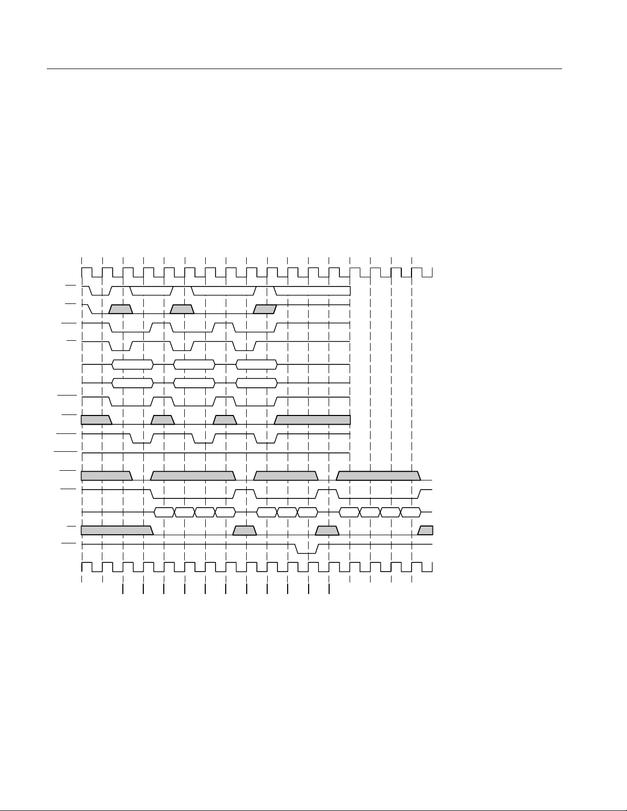
1 10 11 12 13 14 15 16
234 5678 9
SYSCLK
BR
BG
ABB
TS
A[0:31]
TT[0:4]
TBST
GBL
AACK
ARTRY
DBG
CPU A
Read
The following section shows timing diagram and tables that list detail about how
you acquire the relevant address, data, and control signals in 60X bus mode.
Figure 2--1 shows the 60X bus mode timing diagram.
17
CPU A
Write
CPU A
Read
DBB
D[0:63]
TA
TEA
SYSCLK
234 5678 9
1
A
In 0 In 1 In 2 In 3
C
B
A
C
Figure 2--1: 60X bus timing diagram
The Custom Clock uses the rising edge of the SYSCLK.
Delayed signals. BR_ and BG_ are delayed by one clock. Table 2--5 shows the
sample points that are used in MPC7410 60X bus mode.
2-- 10
CC
Out 1 Out 2
Out 0
10 11 12 13 14 15 16
CC
C
A
B
D
In 0 In 1 In 2In3
17
B
TMS546 MPC7XX/MPC74XX Microprocessor Software Support
Page 39

Table 2--5: Sample points in 60X bus-mode
Sample point Signals
Master sample point, M AACK_, ARTRY_, SHD_/SHD[0], TA_, TS_, TEA_,
Sample point, DataArbiter DBG_=, DBG_, DBWO_
Sample point, AddrAttr BR_, BG_, ABB_, A32, A33, A34, A35, A3, A2, A1, A0, TT0,
Sample point, DataAttr DL[0--31], DH[0--31], DBB_
Table 2--6 describes how the signals are stored based on the qualifier signal
levels.
Table 2--6: Signal acquisition for MPC7410 60X bus mode
Acquiring and Viewing Disassembled Data
DRTRY_/DTI[1], AMON_, DMON_, DTI[0], DTI[2], SHD[1],
HRESET_, DRDY_
TT1, TT2, TT3, TT4, TBST_, TSIZ0, TSIZ1,TSIZ2, GBL_, WT_,
CI_
Qualifiers Operation Signals Position
TS_ = LOW Sample AddrAttr and
Master
DBB_ = HIGH and
ARTRY_ = HIGH
TA_ = LOW Sample DataAttr and
TS_= LOW and
TA_ = LOW
AACK_ Sample AddrAttr,
Sample DataArbiter DBG_=, DBG_, DBWO_ Position B
Master
Sample AddrAttr,
DataAttr and Master
DataAttr and Master
BR_, BG_, ABB_, A32, A33, A34, A35, A3, A2, A1, A0,
TT0, TT1, TT2, TT3, TT4, TBST_, TSIZ0, TSIZ1, TSIZ2,
GBL_, WT_, CI_
AACK_, ARTRY_, SHD_/SHD[0], TA_, TS_, TEA_,
DRTRY_/DTI[1], AMON_, DMON_, DTI[0], DTI[2],
SHD[1], HRESET_, DRDY_
DL[0--31], DH[0--31], DBB_, AACK_, ARTRY_,
SHD_/SHD[0], TA_, TS_, TEA_, DRTRY_/DTI[1],
AMON_, DMON_, DTI[0], DTI[2], SHD[1], HRESET_,
DRDY_
BR_, BG_, ABB_, A32, A33, A34, A35, A3, A2, A1, A0,
TT0, TT1, TT2, TT3, TT4, TBST_, TSIZ0, TSIZ1, TSIZ2,
GBL_, WT_, CI_, DL[0--31], DH[0--31], DBB_,
AACK_, ARTRY_, SHD_/SHD[0], TA_, TS_, TEA_,
DRTRY_/DTI[1], AMON_, DMON_, DTI[0], DTI[2],
SHD[1], HRESET_, DRDY_
BR_, BG_, ABB_, A32, A33, A34, A35, A3, A2, A1, A0,
TT0, TT1, TT2, TT3, TT4, TBST_, TSIZ0, TSIZ1, TSIZ2,
GBL_, WT_, CI_, DL[0--31], DH[0--31], DBB_,
AACK_, ARTRY_, SHD_/SHD[0], TA_, TS_, TEA_,
DRTRY_/DTI[1], AMON_, DMON_, DTI[0], DTI[2],
SHD[1], HRESET_, DRDY_
Position A
Position C
When address
tenure for next
transaction starts
before the previous data tenure
completes (not
shown in figure).
Address
acknowledge
cycle.
TMS546 MPC7XX/MPC74XX Microprocessor Software Support
2-- 11
Page 40

Acquiring and Viewing Disassembled Data
Table 2--6: Signal acquisition for MPC7410 60X bus mode (Cont.)
Qualifiers PositionSignalsOperation
ARTRY_ Sample AddrAttr,
DataAttr and Master
DRTRY_/DTI[1]_ = LOW Sample AddrAttr,
DataAttr and Master
TEA_ = LOW Sample AddrAttr,
DataAttr and Master
MPX Bus Mode
Description
The following section shows tables that list details about how you acquire the
relevant address, data, and control signals in MPX bus mode. A complete MPX
bus timing diagram was not available at the time of printing.
The Custom clocking uses the rising edge of the SYSCLK.
BR_, BG_, ABB_, A32, A33, A34, A35, A3, A2, A1, A0,
TT0, TT1, TT2, TT3, TT4, TBST_, TSIZ0, TSIZ1, TSIZ2,
GBL_, WT_, CI_, DL[0--31], DH[0--31], DBB_,
AACK_, ARTRY_, SHD_/SHD[0], TA_, TS_, TEA_,
DRTRY_/DTI[1], AMON_, DMON_, DTI[0], DTI[2],
SHD[1], HRESET_, DRDY_
BR_, BG_, ABB_, A32, A33, A34, A35, A3, A2, A1, A0,
TT0, TT1, TT2, TT3, TT4, TBST_, TSIZ0, TSIZ1, TSIZ2,
GBL_, WT_, CI_, DL[0--31], DH[0--31], DBB_,
AACK_, ARTRY_, SHD_/SHD[0], TA_, TS_, TEA_,
DRTRY_/DTI[1], AMON_, DMON_, DTI[0], DTI[2],
SHD[1], HRESET_, DRDY_
BR_, BG_, ABB_, A32, A33, A34, A35, A3, A2, A1, A0,
TT0, TT1, TT2, TT3, TT4, TBST_, TSIZ0, TSIZ1, TSIZ2,
GBL_, WT_, CI_, DL[0--31], DH[0--31], DBB_,
AACK_, ARTRY_, SHD_/SHD[0], TA_, TS_, TEA_,
DRTRY_/DTI[1], AMON_, DMON_, DTI[0], DTI[2],
SHD[1], HRESET_, DRDY_
Address retry
operation (not
shown in figure)
Data retry
operation (not
shown in figure)
Transfer error
operation
Position D
2-- 12
Delayed Signals. BR_ and BG_ signals are delayed by one clock.
Table 2--7 shows the sample points, that are used in MPC7410 MPX bus mode.
Table 2--7: Sample points in MPX bus mode
Sample point Signals
Master sample point, M AACK_, ARTRY_, SHD_/SHD[0], TA_, TS_, TEA_,
DRTRY_/DTI[1], AMON_, DMON_, SHD[1], HRESET_, DRDY_
Sample point, DataArbiter DBG_=, DBG_, DBWO_, DTI[0]. DRTRY_/DTI[1], DTI[2], DTI[3]
Sample point, AddrAttr BR_, BG_, ABB_, A32, A33, A34, A35, A3, A2, A1, A0, TT0,
TT1, TT2, TT3, TT4, TBST_, TSIZ0, TSIZ1,TSIZ2, GBL_, WT_,
CI_
Sample point, DataAttr DL[0--31], DH[0--31], DBB_
TMS546 MPC7XX/MPC74XX Microprocessor Software Support
Page 41

Acquiring and Viewing Disassembled Data
Table 2--8 describes how the signals are stored based on the qualifier signal
levels.
Table 2--8: Signal acquisition for MPC7410 MPX bus mode
Qualifiers Operation Signals Position
TS_ = LOW Sample AddrAttr and Mas-
ter
DBG_ = HIGH and
ARTRY_ = HIGH
TA_ = LOW Sample DataAttr and Mas-
TS_ = LOW and
TA_ = LOW
AACK_ Sample AddrAttr, DataAttr
ARTRY_ Sample AddrAttr, DataAttr
DRDY_ = LOW Sample AddrAttr, DataAttr
TEA_ = LOW Sample AddrAttr, DataAttr
Sample DataArbiter DBG_=, DBG_, DBWO_, DTI[0]. DRTRY_/DTI[1], DTI[2],
ter
Sample AddrAttr, DataAttr
and Master
and Master
and Master
and Master
and Master
BR_, BG_, ABB_, A32, A33, A34, A35, A3, A2, A1, A0,
TT0, TT1, TT2, TT3, TT4, TBST_, TSIZ0, TSIZ1, TSIZ2,
GBL_, WT_, CI_, AACK_, ARTRY_, SHD_/SHD[0], TA_,
TS_, TEA_, DRTRY_/DTI[1], AMON_, DMON_, DTI[0],
DTI[2], SHD[1], HRESET_, DRDY_.
DTI[3]
DL[0--31], DH[0--31], DBB_, AACK_, ARTRY_,
SHD_/SHD[0], TA_, TS_, TEA_, DRTRY_/DTI [1],
AMON_, DMON_, DTI[0], DTI[2], SHD[1], HRESET_,
DRDY_.
BR_, BG_, ABB_, A32, A33, A34, A35, A3, A2, A1, A0,
TT0, TT1, TT2, TT3, TT4, TBST_, TSIZ0, TSIZ1, TSIZ2,
GBL_, WT_, CI_, DL[0--31], DH[0--31], DBB_,
AACK_, ARTRY_, SHD_/SHD[0], TA_, TS_, TEA_,
DRTRY_/DTI[1], AMON_, DMON_, DTI[0], DTI[2],
SHD[1], HRESET_, DRDY_
BR_, BG_, ABB_, A32, A33, A34, A35, A3, A2, A1, A0,
TT0, TT1, TT2, TT3, TT4, TBST_, TSIZ0, TSIZ1, TSIZ2,
GBL_, WT_, CI_, DL[0--31], DH[0--31], DBB_,
AACK_, ARTRY_, SHD_/SHD[0], TA_, TS_, TEA_,
DRTRY_/DTI[1], AMON_, DMON_, DTI[0], DTI[2],
SHD[1], HRESET_, DRDY_
BR_, BG_, ABB_, A32, A33, A34, A35, A3, A2, A1, A0,
TT0, TT1, TT2, TT3, TT4, TBST_, TSIZ0, TSIZ1, TSIZ2,
GBL_, WT_, CI_, DL[0--31], DH[0--31], DBB_,
AACK_, ARTRY_, SHD_/SHD[0], TA_, TS_, TEA_,
DRTRY_/DTI[1], AMON_, DMON_, DTI[0], DTI[2],
SHD[1], HRESET_, DRDY_
BR_, BG_, ABB_, A32, A33, A34, A35, A3, A2, A1, A0,
TT0, TT1, TT2, TT3, TT4, TBST_, TSIZ0, TSIZ1, TSIZ2,
GBL_, WT_, CI_, DL[0--31], DH[0--31], DBB_,
AACK_, ARTRY_, SHD_/SHD[0], TA_, TS_, TEA_,
DRTRY_/DTI[1], AMON_, DMON_, DTI[0], DTI[2],
SHD[1], HRESET_, DRDY_
BR_, BG_, ABB_, A32, A33, A34, A35, A3, A2, A1, A0,
TT0, TT1, TT2, TT3, TT4, TBST_, TSIZ0, TSIZ1, TSIZ2,
GBL_, WT_, CI_, DL[0--31], DH[0--31], DBB_,
AACK_, ARTRY_, SHD_/SHD[0], TA_, TS_, TEA_,
DRTRY_/DTI[1], AMON_, DMON_, DTI[0], DTI[2],
SHD[1], HRESET_, DRDY_
TMS546 MPC7XX/MPC74XX Microprocessor Software Support
2-- 13
Page 42

Acquiring and Viewing Disassembled Data
Signal Acquisition with MPC7410_ALT and MPC7410_QD Support
This section describes signal acquisition for the MPC7410_ALT and
MPC7410_QD support.
No delayed signals are used in these supports. In custom clocking, the module
clocking state machine (CSM) generates one master sample for every rising edge
of the system clock. All signals are acquired at this master sample point.
Viewing Disassembled Data
You can view disassembled data in four display formats: Hardware, Software,
Control Flow, and Subroutine. The information on basic operations describes
how to select the disassembly display formats.
NOTE. Selections in the Disassembly property page (the Disassembly Format
Definition overlay) must be set correctly for your acquired data to be disassembled correctly. Refer to Changing How Data is Displayed on page 2--21.
For MPC7410, the default display format shows the Address, High_Data,
Low_Data, and TraceAddr channel group values for each sample of acquired
data.
For MPC7450, the default display format shows the MSB_Addr, Address,
High_Data, Low_Data, and TraceAddr channel group values for each sample of
acquired data.
For the MPC7410_ALT and MPC7410_QD supports, the default display format
shows Address, High_Data, Low_Data, TraceAddr channel group values for each
sample of acquired data.
If a channel group is not visible, you must use Add Column or Ctrl+L to make
the group visible.
The disassembler displays special characters and strings in the instruction
mnemonics to indicate significant events. Table 2--9 shows these special
characters and strings and gives a definition of what they represent.
Table 2--9:
Character or string displayed Description
>> The instruction was manually marked
Description of special characters in the display
2-- 14
**** Indicates there is insufficient data available for complete
disassembly of the instruction; the number of asterisks
indicates the width of the data that is unavailable. Every two
asterisks represent one byte.
TMS546 MPC7XX/MPC74XX Microprocessor Software Support
Page 43

Acquiring and Viewing Disassembled Data
Hardware Display Format
Table 2--9:
Character or string displayed Description
# Indicates an immediate value
> Insufficient room on the screen to show all available data.
t Indicates the given number is in decimal. Example: #12t (for
Description of special characters in the display (cont.)
0xC in hexadecimal)
In Hardware display format, all valid opcode fetch bus cycles will be disassembled and displayed. Noninstruction bus cycles will be displayed with the
appropriate Cycle Type label. In Hardware display format, the disassembler
displays certain cycle type labels in parentheses.
Table 2--10 the cycle type labels and definitions for Address sequences.
Table 2--10: Cycle type labels for Address sequences and definitions
Cycle type label Definition
( Address ) Address cycle with selected processor
( Address only--clean block ) Address only cycle
( Address only--flush block ) Address only cycle
( Address only--sync ) Address only cycle
( Address only--kill block ) Address only cycle
( Address only--eieio ) Address only cycle
( Address only--tlb invalidate ) Address only cycle
( Address only--lwarx ) Address only cycle
( Address only--tlbsync ) Address only cycle
( Address only--icbi ) Address only cycle
( Address only--reserved ) Address only cycle
( Address retry ) Address retry cycle for selected master
( Alt address ) Alternate master address cycle
( Alt address retry ) Alternate master address retry cycle
( Alt address acknowledge ) Alternate master address acknowledge cycle
( Address acknowledge ) Address acknowledge cycle for selected master
TMS546 MPC7XX/MPC74XX Microprocessor Software Support
2-- 15
Page 44

Acquiring and Viewing Disassembled Data
Table 2--11 shows the cycle type labels and definitions for Data sequences.
Table 2--11: Cycle type labels for Data sequences and definitions
Cycle type label Definition
( External--control--word--write ) External control word write operation
( External--control--word--read ) External control word read operation
( Write--with--flush ) Write with flush operation
( Write--with--kill ) Write with kill operation
( Read ) Data read cycle
( Read--with--intent--to--modify ) Read with intent to modify operation
( Write--with--flush--atomic ) Write with flush atomic operation
( Read--atomic ) Read atomic operation
( Read--with--intent--to--modify--atomic ) Read with intent to modify atomic operation
( R e a d -- w i t h -- n o -- i n t e n t -- t o -- c a c h e ) Read with no intent to cache
( Read-claim) Read claim operation
( Reserved--transfer--type ) Reserved transfer type
( Flush ) Flush cycle because of change in execution flow
( Data only ) Data only cycle
(Altdata) Alternate master data. This is applicable when the
number of processors used is ‘Greater than 2’.
( Transfer error ) Data error cycle for selected master
( Alt Transfer Error ) Alternate data error
( Data retry ) Data retry cycle for selected master
( Alt Data retry ) Alternate master data retry cycle
( Cache line fill ) In a 32-byte burst transaction, the disassembly displays
information only for critical words. The other data beats
for that transaction are displayed as cache line fills.
( Alt Cache line fill ) Cache line fill labels displayed if alternate master is
selected.
( Data Invalid ) This label is displayed when an address retry has
occurred and Data for that address still appears. Those
Data cycles are labeled as Data Invalid for selected
master.
( Alt Data Invalid ) Data Invalid labels displayed if alternate master is
selected.
2-- 16
TMS546 MPC7XX/MPC74XX Microprocessor Software Support
Page 45

Acquiring and Viewing Disassembled Data
Table 2--12 shows General cycle type labels and definitions.
Table 2--12: General cycle type labels definitions
Cycle type label Definition
( System reset ) System reset cycle
( Unknown ) Unknown cycle
( Word $Hexvalue ) This label is displayed if the cycle is identified as a Fetch
but the Opcode is Invalid. the Hexvalue following the $
symbol gives the value of the Opcode.
***Un-associated data*** This label is displayed when there is no address to
associate for a data beat (because of incomplete
acquisition of the complete cycle) or when the address is
retried and data tenure already started. Refer to the
following section on Address Pipelining for more details.
( Idle cycle ) Processor idle cycle
Address Pipelining. TMS546 is designed to support up to 16-level address
pipeline. The disassembler, by default, starts associating first acquired address
tenure with first acquired data tenure. But if the system is doing address
pipelining, and if the all the address tenures were not acquired in the refmem (at
start of refmem) then there will be data tenures without address tenure to
associate. Such data tenures are labeled as “*** Un-associated data ***” in the
disassembly. When you find this label in the acquisition, it means that all the data
tenure previous to this sample are associated with wrong address tenure. To get
correct address associated data tenure, use the marking option ”Invalid data”
provided. You must mark all the data tenures which are associated with wrong
address tenures at the start of the acquisition as ”Invalid data”. Once you
associate an address tenure with the correct data tenure, the disassembly adjusts
itself for the change in the pipeline depth.
TMS546 MPC7XX/MPC74XX Microprocessor Software Support
2-- 17
Page 46

Acquiring and Viewing Disassembled Data
Figure 2--2 displays an example of data in the Hardware Display format.
Figure 2--2: Example of Hardware display format
Software Display Format
The Software display format shows only the first opcode fetch of executed
instructions. Flushed cycles and extensions are not displayed, even though they
are part of the executed instruction. Data reads and writes are not displayed.
Any ‘special’ cycles that are described as displayed in Control Flow Display or
Subroutine Display Formats are displayed.
2-- 18
TMS546 MPC7XX/MPC74XX Microprocessor Software Support
Page 47

Acquiring and Viewing Disassembled Data
Figure 2--3 displays an example of data in the Software Display format.
Figure 2--3: Example of Software display format
Control Flow Display
Format
The Control Flow display format shows only the first opcode fetch of instructions that cause a branch in the addressing.
Instructions that unconditionally generate a change in the flow of control in the
TMS546 MPC7410 microprocessor are as follows:
b target ba target
bl target bla target
sc rfi
TMS546 MPC7XX/MPC74XX Microprocessor Software Support
2-- 19
Page 48

Acquiring and Viewing Disassembled Data
Instructions that might conditionally generate a change in the flow of control in
the TMS546 MPC7410 microprocessor are as follows:
bc BO,BI,target bca BO,BI,target
bcl BO,BI,target bcla BO,BI,target
bclr BO,BI bclrl BO,BI
bcctr BO,BI bcctrl BO,BI
isync tw
twi
Figure 2--4 displays an example of data in the Control Flow data format.
Figure 2--4: Example of Control Flow display format
Subroutine Display
Format
2-- 20
The Subroutine display format shows only the first opcode fetch of the subroutine call and return instructions. It displays conditional subroutine calls if they are
considered to be taken.
Instructions that unconditionally generate a subroutine call or a return in the
TMS546 MPC7410 microprocessor are as follows:
sc rfi
TMS546 MPC7XX/MPC74XX Microprocessor Software Support
Page 49

Acquiring and Viewing Disassembled Data
Instructions that conditionally generate a subroutine call or a return in the
TMS546 MPC7410 microprocessor are as follows:
isync tw twi
Figure 2--5 displays an example of data in the Subroutine Display format.
Figure 2--5: Example of Subroutine display format
Changing How Data is Displayed
There are common fields and features that allow you to further modify displayed
data to suit your needs. You can make common and optional display selections in
the Disassembly property page (the Disassembly Format Definition overlay).
You can make selections unique to the TMS546 MPC7410 support to do the
following tasks:
H Change how data is displayed across all display formats
H Change the interpretation of disassembled cycles
H Display exception cycles
TMS546 MPC7XX/MPC74XX Microprocessor Software Support
2-- 21
Page 50

Acquiring and Viewing Disassembled Data
Optional Display
Selections
Micro Specific Fields for
MPC7410 Support
Table 2--13 shows the logic analyzer disassembly display options.
Table 2--13: Logic analyzer disassembly display options
Description Option
Show: Hardware (Default)
Software
Control Flow
Subroutine
Highlight: Software (Default)
Control Flow
Subroutine
None
Disasm Across Gaps: Yes
No (Default)
Along with the optional selections described in the logic analyzer help, you can
change the displayed data in the following ways.
Bus Protocol. The MPC7410 supports PowerPCs which support both 60X bus
protocol and MPX bus protocol.
Select the mode that the processor operates in by selecting one of the two
available options.
Bus Protocol: 60X (default)
MPX
Select the 60X option when the processor is working in the 60X mode and the
MPX option when the processor is working in the MPX mode.
Number of Processors. The TMS546 MPC7410 microprocessor support provides
simultaneous disassembly for a maximum of two processors at a time in 60X bus
mode. In MPX bus mode, only one processor can be disassembled at a time. If
more than two processors are used, then the transactions of the processor other
than the one being probed are labeled as Alternate Master Transactions. You can
select one of the options:
H Select One if the system contains one processor and one or more other
masters (default).
H Select Two-PPC0 if the system contains two processors and both are
PowerPC processors, disassemble PPC0.
2-- 22
TMS546 MPC7XX/MPC74XX Microprocessor Software Support
Page 51

Acquiring and Viewing Disassembled Data
H Select Two-PPC1 if the system contains two processors and both are
PowerPC processors, disassemble PPC1.
H Select Three or more if the system contains three or more masters.
NOTE. PPC0 is the PowerPC processor from where the signals are being probed.
(In that case PPC0 is the master). PPC1 is the other PowerPC processor, which
is connected to the same bus in a multiprocessor environment.
When option “Two-PPC0” is selected, the cycles from PPC0 are disassembled
and PPC1 cycles are displayed as Alternate cycles. Similarly, when option
“Two-PPC1” is selected, the cycles from PPC1 are disassembled and PPC0
cycles are displayed as Alternate cycles.
When option “Three or More” is selected, the disassembler shows cycles from
PPC0 and all the other cycles from other processors are shown as Alternate
cycles.
Processor to Disassemble. Select the processor for the appropriate disassembly
support by selecting one of the five available options.
H Select MPC7X0 when the processor to disassemble is MPC740/MPC750
(default).
H Select MPC7X5 when the processor to disassemble is
MPC745/755/PPC750FX.
H Select MPC7400 when the processor to disassemble is MPC7400.
H Select MPC7410 when the processor to disassemble is MPC7410.
H Select MPC7450 when the processor to disassemble is
MPC7450/7451/7455/7441/7445.
H Select PPC750CX when the processor to disassemble is PPC750CX.
Data Bus Mode. MPC745 and MPC755 data bus width is selectable between
32-bit and 64-bit widths. Select the bus mode by selecting one of the two
available options.
Data Bus Mode: 64 bit (default)
32 bit
TMS546 MPC7XX/MPC74XX Microprocessor Software Support
2-- 23
Page 52

Acquiring and Viewing Disassembled Data
NOTE. All the other processors supported in TMS546 MPC7410 use only the
64-bit data bus.
Prefetch Byte Ordering. Byte ordering for the Predominant Instruction Fetches is
selected by selecting one of the two available options.
Prefetch Byte Ord: Big Endian (default)
Alternate Byte Ordering Alternate Byte ordering range is supplied by entering the
proper 32-bit hexadecimal values in the fill-in fields:
Alt Byte Ord -- Lo Bound 00000000 (default)
Alt Byte Ord -- Hi Bound 00000000 (default)
NOTE. Hi Bound Value must be greater than Lo Bound Value, otherwise an
erroneous display may result. Values entered are preferred on double word
boundaries — if any other value is entered, that value defaults to the nearest
double word value. If nothing is entered in the Hi Bound and Lo Bound fields,
then the byte ordering that is selected under Prefetch Byte ordering is assumed
for the entire acquisition. For the range supplied for alternate byte ordering, the
byte ordering opposite to that selected for Prefetch Byte Ordering is assumed.
PowerPC Little Endian
2-- 24
Exception Byte Ordering. Select Byte Ordering for Exception processing by
selecting one of the two available options.
Exception Byte Ord: Big Endian (default)
PowerPC Little Endian
Exception Prefix. Select a valid Exception Prefix by selecting one of the two
available options depending on the system used.
Exception Prefix : 000 (default)
FFF
NOTE. If an address is in both, the exception processing region of the processor
and the range selected for the alternate byte ordering, then the byte ordering
selected for the exception processing is assumed for that address.
TMS546 MPC7XX/MPC74XX Microprocessor Software Support
Page 53

Acquiring and Viewing Disassembled Data
Trace Write Address. This field contains the Trace Write address in use. Enter the
noncacheable address to which the exception handler writes the SRR0 content.
This is required for ITR.
Memory Image Status. When you choose the Enabled option, you cannot edit or
modify the S-Record (Image File currently in use). You must choose the Disabled
option to edit or modify the S-record.
Memory Image Status: Enabled (default)
Disabled
Disassemble Based On. This option allows you to select the basis for disassembly.
If you choose the option Fetch Stream, normal disassembly occurs. When you
select the Memory Image option, disassembly is based on the image file. For
example, S-record file has two options:
Disassemble Based On: Fetch Stream (default)
Memory Image
Image File Path. You need to enter the complete path to the S-record file in the
property for Image file path. Use the Browse button for this. By default, this field
is blank.
Address Offset in Hex. This is the address offset (in hexadecimal) from the
starting address (as indicated by the S-record) where the user program is loaded
in memory. By default this is 0x00000000.
Suppose the linker output and the corresponding S-record file has a starting
address of 0x0, but you load it at a different address. For example, if you load the
starting address at 0x50, you then need to specify the offset—0x50 as
0xFFFFFFB0 in this field.
H When the S-record address is less than the Processor_Address, then the
Address_Offset must be negative.
H When the S-record address is greater than the Processor_Address, then the
Address_Offset must be positive.
So the correspondence intended is:
Processor_Address + Address_Offset == S_Record_Address:
Maximum Instructions. Enter the number of instructions to be displayed (from the
image file each time a BTE is encountered) in the property for Maximum
Instructions. This is required for ITR. The default is 40. This is the maximum
number of instructions that is taken from the image file to show each time a
control flow change occurs.
TMS546 MPC7XX/MPC74XX Microprocessor Software Support
2-- 25
Page 54

Acquiring and Viewing Disassembled Data
Track Radix Of. Select which column the mnemonics is formatted in. This field
has two options.
Track Radix Of: Address (default)
This submenu has the title: “MPC7410 Controls”.
TraceAddr
Micro Specific Fields for
MPC7450 Support
Along with the optional selections described in the logic analyzer help, you can
change the displayed data in the following ways.
Bus Protocol. The MPC7450 supports PowerPC’s for both the 60X bus protocol
and the MPX bus protocol.
Select the mode that the processor operates by selecting one of the two available
options.
Bus Protocol: 60X (default)
MPX
Select the 60X option when the processor is working in 60X mode (default) and
the MPX option when the processor is working in MPX mode.
Number of Processors. The TMS546 MPC7410 microprocessor support provides
simultaneous disassembly for a maximum of two processors at a time in 60X bus
mode. In MPX bus mode, only one processor can be disassembled at a time. If
more than two processors are used, then the transactions of the processor other
than the one being probed are labeled as Alternate Master Transactions. You can
select one of the options:
H Select One if the system contains one processor and one or more other
masters (default).
2-- 26
H Select Two-PPC0 if the system contains two processors and both are
PowerPC processors, disassemble PPC0.
H Select Two-PPC1 if the system contains two processors and both are
PowerPC processors, disassemble PPC1.
H Select Three or more if the system contains three or more masters.
NOTE. PPC0 is the PowerPC processor from where the signals are being probed.
(In that case PPC0 is the master). PPC1 is the other PowerPC processor (which
must be another MPC7450 PowerPC processor) that is connected to the same
bus in a multiprocessor environment.
TMS546 MPC7XX/MPC74XX Microprocessor Software Support
Page 55

Acquiring and Viewing Disassembled Data
Prefetch Byte Ordering. Byte ordering for the Predominant Instruction Fetches is
selected by selecting one of the two available options.
Prefetch Byte Ord: Big Endian (default)
PowerPC Little Endian
Alternate Byte Ordering. Alternate Byte ordering range is supplied by entering the
proper 32-bit hexadecimal values in the fill-in fields:
Alt Byte Ord -- Lo Bound 00000000 (default)
Alt Byte Ord -- Hi Bound 00000000 (default)
NOTE. Hi Bound Value must be greater than Lo Bound Value, otherwise an
erroneous display may result. Values entered are preferred on double word
boundaries — if any other value is entered, that value defaults to the nearest
double word value. If nothing is entered in the Hi Bound and Lo Bound fields,
then the byte ordering that is selected under Prefetch Byte ordering is assumed
for the entire acquisition. For the range supplied for alternate byte ordering, the
byte ordering opposite to that selected for Prefetch Byte Ordering is assumed.
Exception Byte Ordering. Select Byte Ordering for Exception processing by
selecting one of the two available options.
Exception Byte Ord: Big Endian (default)
PowerPC Little Endian
Exception Prefix. Select a valid Exception Prefix by selecting one of the two
available options depending on the system used.
Exception Prefix : 000 (default)
FFF
NOTE. If an address is in both the Exception processing region of the processor
and in the range selected for the alternate byte ordering, then the byte ordering
selected for the Exception processing is assumed for that address.
Trace Write Address. This field contains the Trace Write address in use. Enter the
noncacheable address to which the exception handler writes the SRR0 content.
This is required for ITR.
TMS546 MPC7XX/MPC74XX Microprocessor Software Support
2-- 27
Page 56

Acquiring and Viewing Disassembled Data
Memory Image Status. When you choose the Enabled option, you cannot edit or
modify the S-Record (Image File currently in use). You must choose the Disabled
option to edit or modify the S-record.
Memory Image Status: Enabled (default)
Disassemble Based On. This option allows you to select the basis for disassembly.
If you choose the option Fetch Stream, normal disassembly occurs. When you
select the Memory Image option, disassembly is based on the image file. For
example, S-record file has two options:
Disassemble Based On: Fetch Stream (default)
Image File Path. You need to enter the complete path to the S-record file in the
property for Image file path. Use the Browse button for this. By default, this field
is blank.
Disabled
Memory Image
Address Offset in Hex. This is the address offset (in hexadecimal) from the
starting address (as indicated by the S-record) where the user program is loaded
in memory. By default this is 0x00000000.
Suppose the linker output and the corresponding S-record file has a starting
address of 0x0, but you load it at a different address. For example, at 0x50, you
then need to specify the offset—0x50 as 0xFFFFFFB0 in this field.
H When the S-record address is less than the Processor_Address, then the
Address_Offset must be negative.
H When the S-record address is greater than the Processor_Address, then the
Address_Offset must be positive.
So the correspondence intended is:
Processor_Address + Address_Offset == S_Record_Address:
Maximum Instructions. Enter the number of instructions to be displayed (from the
image file each time a BTE is encountered) in the property for Maximum
Instructions. This is required for ITR. The default is 40. This is the maximum
number of instructions that is taken from the image file to show each time a
control flow change occurs.
2-- 28
TMS546 MPC7XX/MPC74XX Microprocessor Software Support
Page 57

Acquiring and Viewing Disassembled Data
Track Radix Of. Select which column the mnemonics is formatted in. This has two
options.
Track Radix Of: Address (default)
TraceAddr
This submenu has the title: “MPC7450 Controls”.
Micro Specific Fields for
MPC7410_ALT Support
Along with the optional selections described in the logic analyzer help, you can
change the displayed data in the following ways:
Idle Cycles. Since this is a clock-by-clock acquisition, many idle cycles are
acquired. Select this option to show or suppress idle cycles.
Idle Cycles: Show (default)
Suppress
Bus Protocol. The MPC7410_ALT supports PowerPCs for both the 60X bus
protocol and the MPX bus protocol.
Select the mode that the processor operates by selecting one of the two available
options.
Bus Protocol: 60X (default)
MPX
Select the 60X option when the processor is working in 60X mode (default) and
the MPX option when the processor is working in MPX mode.
Number of Processors. The MPC7410_ALT support provides simultaneous
disassembly for a maximum of two processors. If more than two processors are
used, then the transactions of the processor other than the one being probed are
labeled as Alternate Master Transactions. You can select one of the options:
H Select One if the system contains one processor and one or more other
masters (default).
H Select Two-PPC0 if the system contains two processors and both are
PowerPC processors, disassemble PPC0.
H Select Two-PPC1 if the system contains two processors and both are
PowerPC processors, disassemble PPC1.
H Select Three or more if the system contains three or more masters.
TMS546 MPC7XX/MPC74XX Microprocessor Software Support
2-- 29
Page 58

Acquiring and Viewing Disassembled Data
NOTE. PPC0 is the PowerPC processor from where the signals are being probed.
(In that case PPC0 is the master). PPC1 is the other PowerPC processor, which
is connected to the same bus in a multiprocessor environment.
When option “Two-PPC0” is selected, the cycles from PPC0 are disassembled
and PPC1 cycles are displayed as Alternate cycles. Similarly, when option
“Two-PPC1” is selected, the cycles from PPC1 are disassembled and PPC0
cycles are displayed as Alternate cycles.
When option “Three or More” is selected, the disassembler shows cycles from
PPC0 and all the other cycles from other processors are shown as Alternate
cycles.
To view disassembly of other processors in a multiprocessor system, add new
listing windows and select the processor to disassemble in Disassembly User
option. Use Ctrl+N to activate the new window wizard and select the correct
disassembly options.
Processor to Disassemble. Select the processor for the appropriate disassembly
support by selecting one of the three available options.
H Select MPC7400 when the processor to disassemble is MPC7400.
H Select MPC7410 when the processor to disassemble is MPC7410.
H Select MPC7450 when the processors to disassemble are MPC7450,
MPC7455, MPC7441, and MPC7445.
Pipeline – Out of Order. The two signal groups — DTI and ODT, are used when
the target system performs pipeline and out of order. Some systems provide only
DTI signal group. You can select one of these depending on your target system
configuration. If your target system has only DTI, use “Invalid Data” marking
option to associate the data with the correct address. If the DTI values of data
arriving after the marked sample are higher than that of the marked sample, then
the data is associated correctly with the address tenure.
H Use DTI alone: (default) when the target system does not have ODT signals
from the system arbiter.
H Use ODT and DTI: when the target system does not have ODT signals from
the arbiter.
2-- 30
ODT Timing. ODT signal groups can be valid either with bus grant or with one
clock after a qualified bus grant. Select this option according to your target
system’s setting.
TMS546 MPC7XX/MPC74XX Microprocessor Software Support
Page 59

Acquiring and Viewing Disassembled Data
ODT Timing: ODT on Bus Grant (default)
Delayed ODT
DTI Configuration. Multiprocessor systems with different DTI configurations are
available. DTIs can be either bussed (to reflect the DTI value when the other
master is using the bus) or configured point to point. In point to point configuration, the DTI value of masters are not visible each other. Select this option
according to your target system’s configuration. For bussed DTI signals, then the
target system’s DTI signals must be connected to DTI channels with the prefix
P0.
DTI Configuration: Bussed (default)
Point-to-point
Prefetch Byte Ordering. Byte ordering for the Predominant Instruction Fetches is
selected by selecting one of the two available options.
Prefetch Byte Ord: Big Endian (default)
PowerPC Little Endian
Alternate Byte Ordering. Alternate Byte ordering range is supplied by entering the
proper 32-bit hexadecimal values in the fill-in fields:
Alt Byte Ord -- Lo Bound 00000000 (default)
Alt Byte Ord -- Hi Bound 00000000 (default)
NOTE. Hi Bound Value must be greater than Lo Bound Value, otherwise an
erroneous display may result. Values entered are preferred on double word
boundaries — if any other value is entered, that value defaults to the nearest
double word value. If nothing is entered in the Hi Bound and Lo Bound fields,
then the byte ordering that is selected under Prefetch Byte ordering is assumed
for the entire acquisition. For the range supplied for alternate byte ordering, the
byte ordering opposite to that selected for Prefetch Byte Ordering is assumed.
Exception Byte Ordering. Select Byte Ordering for Exception processing by
selecting one of the two available options.
Exception Byte Ord: Big Endian (default)
PowerPC Little Endian
TMS546 MPC7XX/MPC74XX Microprocessor Software Support
2-- 31
Page 60

Acquiring and Viewing Disassembled Data
Exception Prefix. Select a valid Exception Prefix by selecting one of the two
available options depending on the system used.
Exception Prefix : 000 (default)
NOTE. If an address is in both the Exception processing region of the processor
and in the range selected for the alternate byte ordering, then the byte ordering
selected for the Exception processing is assumed for that address.
Trace Write Address. This field contains the Trace Write address in use. Enter the
noncacheable address to which the exception handler writes the SRR0 content.
This is required for ITR.
Memory Image Status. When you choose the Enabled option, you cannot edit or
modify the S-Record (Image File currently in use). You must choose the Disabled
option to edit or modify the S-record.
FFF
Memory Image Status: Enabled (default)
Disabled
Disassemble Based On. This option allows you to select the basis for disassembly.
If you choose the option Fetch Stream, normal disassembly occurs. When you
select the Memory Image option, disassembly is based on the image file. For
example, S-record file has two options:
Disassemble Based On: Fetch Stream (default)
Memory Image
Image File Path. You need to enter the complete path to the S-record file in the
property for Image file path. Use the Browse button for this. By default, this field
is blank.
Address Offset in Hex. This is the address offset (in hexadecimal) from the
starting address (as indicated by the S-record) where the user program is loaded
in memory. By default this is 0x00000000.
Suppose the linker output and the corresponding S-record file has a starting
address of 0x0, but you load it at a different address. For example, at 0x50, you
then need to specify the offset—0x50 as 0xFFFFFFB0 in this field.
2-- 32
TMS546 MPC7XX/MPC74XX Microprocessor Software Support
Page 61

Acquiring and Viewing Disassembled Data
H When the S-record address is less than the Processor_Address, then the
Address_Offset must be negative.
H When the S-record address is greater than the Processor_Address, then the
Address_Offset must be positive.
So the correspondence intended is:
Processor_Address + Address_Offset == S_Record_Address:
Maximum Instructions. Enter the number of instructions to be displayed (from the
image file each time a BTE is encountered) in the property for Maximum
Instructions. This is required for ITR. The default is 40. This is the maximum
number of instructions that is taken from the image file to show each time a
control flow change occurs.
Track Radix Of. Select which column the mnemonics is formatted in. This has two
options.
Track Radix Of: Address (default)
TraceAddr
Micro Specific Fields for
MPC7410_QD Support
Along with the optional selections described in the logic analyzer help, you can
change the displayed data in the following ways.
Idle Cycles. Since this is a clock-by-clock acquisition, many idle cycles are
acquired. Select this option to show or suppress idle cycles.
Idle Cycles: Show (default)
Suppress
Bus Protocol. The MPC7410_QD supports PowerPCs for both the 60X bus
protocol and the MPX bus protocol.
Select the mode that the processor operates by selecting one of the two available
options.
Bus Protocol: 60X (default)
MPX
Select the 60X option when the processor is working in 60X mode (default) and
the MPX option when the processor is working in MPX mode.
Disassemble. The MPC7410_QD support provides simultaneous disassembly for
a maximum of four processors. The bus cycles other than those of the selected
processor option are marked as alternate cycles.
TMS546 MPC7XX/MPC74XX Microprocessor Software Support
2-- 33
Page 62

Acquiring and Viewing Disassembled Data
You can select one of the options:
H Select PowerPC P0 to disassemble PowerPC 0 (default).
H Select PowerPC P1 to disassemble PowerPC 1.
H Select PowerPC P2 to disassemble PowerPC 2.
H Select PowerPC P3 to disassemble PowerPC 3.
NOTE. The suffix P
with corresponding processor P
where n=0, 1, 2,or 3corresponds to the point to point signals
n
where n=0, 1, 2, or 3. Bussed signals are
n
common for all selections.
To view disassembly of other processors in a multiprocessor system, add new
listing windows and select the processor to disassemble in Disassembly User
option. Use Ctrl+N to activate the new window wizard and select the correct
disassembly options.
Processor to Disassemble. Select the processor for the appropriate disassembly
support by selecting one of the three available options.
H Select MPC7400 when the processor to disassemble is MPC7400.
H Select MPC7410 when the processor to disassemble is MPC7410.
H Select MPC7450 when the processors to disassemble are MPC7450,
MPC7455, MPC7441, and MPC7445.
Pipeline – OutofOrder.The two signal groups — DTI and ODT, are used when
the target system performs pipeline and out of order. Some systems provide only
DTI signal group. You can select one of these depending on your system
configuration. If your target system has only DTI, use “Invalid Data” marking
option associate the data with the correct address. If the DTI values of data
arriving after the marked sample are higher than that of the marked sample, the
data is associated correctly with the address tenure.
2-- 34
H Use DTI alone (default) when the system does not have ODT signals from
the system arbiter.
H Use ODT and DTI when the system does not have ODT signals from the
arbiter.
TMS546 MPC7XX/MPC74XX Microprocessor Software Support
Page 63

Acquiring and Viewing Disassembled Data
ODT Timing. ODT signal groups can be valid either with bus grant or one clock
after a qualified bus grant. Select this option according to your system setting.
ODT Timing: ODT on Bus Grant (default)
Delayed ODT
DTI Configuration. Multiprocessor systems with different DTI configurations are
available. DTIs can be either bussed (to reflect the DTI value when the other
master is using the bus) or configured point to point. In point to point configuration, the DTI value of masters are not visible each other. Select this option
according to your target system’s configuration. For bussed DTI signals, then the
target system’s DTI signals must be connected to DTI channels with the prefix
P0.
DTI Configuration: Bussed (default)
Point-to-point
Prefetch Byte Ordering. Byte ordering for the Predominant Instruction Fetches is
selected by selecting one of the two available options.
Prefetch Byte Ord: Big Endian (default)
PowerPC Little Endian
Alternate Byte Ordering. Alternate Byte ordering range is supplied by entering the
proper 32-bit hexadecimal values in the fill-in fields:
Alt Byte Ord -- Lo Bound 00000000 (default)
Alt Byte Ord -- Hi Bound 00000000 (default)
NOTE. Hi Bound Value must be greater than Lo Bound Value, otherwise an
erroneous display may result. Values entered are preferred on double word
boundaries — if any other value is entered, that value defaults to the nearest
double word value. If nothing is entered in the Hi Bound and Lo Bound fields,
then the byte ordering that is selected under Prefetch Byte ordering is assumed
for the entire acquisition. For the range supplied for alternate byte ordering, the
byte ordering opposite to that selected for Prefetch Byte Ordering is assumed.
Exception Byte Ordering. Select Byte Ordering for Exception processing by
selecting one of the two available options.
Exception Byte Ord: Big Endian (default)
PowerPC Little Endian
TMS546 MPC7XX/MPC74XX Microprocessor Software Support
2-- 35
Page 64

Acquiring and Viewing Disassembled Data
Exception Prefix. Select a valid Exception Prefix by selecting one of the two
available options depending on the system used.
Exception Prefix : 000 (default)
NOTE. If an address is in both the Exception processing region of the processor
and in the range selected for the alternate byte ordering, then the byte ordering
selected for the Exception processing is assumed for that address.
Trace Write Address. This field contains the Trace Write address in use. Enter the
noncacheable address to which the exception handler writes the SRR0 content.
This is required for ITR.
Memory Image Status. When you choose the Enabled option, you cannot edit or
modify the S-Record (Image File currently in use). You must choose the Disabled
option to edit or modify the S-record.
FFF
Memory Image Status: Enabled (default)
Disabled
Disassemble Based On. This option allows you to select the basis for disassembly.
If you choose the option Fetch Stream, normal disassembly occurs. When you
select the Memory Image option, disassembly is based on the image file. For
example, S-record file has two options:
Disassemble Based On: Fetch Stream (default)
Memory Image
Image File Path. You need to enter the complete path to the S-record file in the
property for Image file path. Use the Browse button for this. By default, this field
is blank.
Address Offset in Hex. This is the address offset (in hexadecimal) from the
starting address (as indicated by the S-record) where the user program is loaded
in memory. By default this is 0x00000000.
Suppose the linker output and the corresponding S-record file has a starting
address of 0x0, but you load it at a different address. For example, at 0x50, you
then need to specify the offset—0x50 as 0xFFFFFFB0 in this field.
2-- 36
TMS546 MPC7XX/MPC74XX Microprocessor Software Support
Page 65

Acquiring and Viewing Disassembled Data
H When the S-record address is less than the Processor_Address, then the
Address_Offset must be negative.
H When the S-record address is greater than the Processor_Address, then the
Address_Offset must be positive.
So the correspondence intended is:
Processor_Address + Address_Offset == S_Record_Address:
Maximum Instructions. Enter the number of instructions to be displayed (from the
image file each time a BTE is encountered) in the property for Maximum
Instructions. This is required for ITR. The default is 40. This is the maximum
number of instructions that is taken from the image file to show each time a
control flow change occurs.
Track Radix Of. Select which column the mnemonics is formatted in. This has two
options.
Track Radix Of: Address (default)
TraceAddr
Marking Cycles
The disassembler has a Mark Opcode function that allows you to change the
interpretation of a cycle type. Using this function, you can select a cycle and
change it.
Logic Analyzer. Marks are placed by using the Mark Opcode button. The Mark
Opcode button is always available. If the sample being marked is not a Data
cycle of the potential bus master, the Mark Opcode selections are replaced by a
note indicating that “An Opcode Mark cannot be placed at the selected data
sample.”
When a cycle is marked, the character “>>” is displayed immediately to the left
of the Mnemonics column. Cycles can be unmarked by using the “Undo Mark”
selection, which removes the character “>>”.
TMS546 MPC7XX/MPC74XX Microprocessor Software Support
2-- 37
Page 66
Acquiring and Viewing Disassembled Data
Mark selections available on data sequences without an address and data cycle
associated with a data cycle for TMS546 MPC7410 microprocessors as shown in
Table 2--14.
Table 2--14: Mark selections and definitions
Mark selection or combination Definition
Opcode -- Opcode High_Data and Low_Data are disassembled
Opcode -- Flush Only High_Data is disassembled in Big Endian mode or only Low_Data is disas-
sembled in Little Endian mode
Flush -- Opcode Only Low_Data is disassembled in Big Endian mode or only High_Data is disas-
sembled in Little Endian mode
Flush -- Flush Instructions not disassembled and labeled as ( Flush )
Read --> Fetch Read is marked as a Fetch
Invalid Data Any of the fetches, read or write can be marked as Invalid Data bits. No address is
associated for this data.
Undo Mark Removes all marks from the current sequence
Information on basic operations contains more details on marking cycles.
Displaying Exception
Labels
The disassembler can display TMS546 MPC7410 exception labels. The
exception table must reside in external memory for interrupt and exception cycles
to be visible to the disassembler.
You can enter the table prefix in the Exception Prefix field. The Exception Prefix
field provides the disassembler with the offset address; enter a three-digit
hexadecimal value corresponding to the prefix of the exception table.
These fields are located in the Disassembly property page (Disassembly Format
Definition overlay).
Table 2--15 lists the TMS546 MPC7410 interrupt and exception labels.
Table 2--15: Interrupt and exception labels
Offset Displayed interrupt or exception name
0x00000 ( Reserved )
0x00100 ( System reset )
0x00200 ( Machine check exception )
0x00300 ( DSI exception )
0x00400 ( ISI exception )
0x00500 ( External interrupt )
2-- 38
TMS546 MPC7XX/MPC74XX Microprocessor Software Support
Page 67

Acquiring and Viewing Disassembled Data
Table 2--15: Interrupt and exception labels (cont.)
Offset Displayed interrupt or exception name
0x00600 ( Alignment exception )
0x00700 ( Program exception )
0x00800 ( Floating-point unavailable exception )
0x00900 ( Decrementer exception )
0x00A00 -- 0x00BFF ( Reserved )
0x00C00 ( System call exception )
0x00D00 ( Trace exception )
0x00E00 ( Reserved )
0x00F00 ( Performance monitor exception )
0x00F20 ( Altivec unavailable exception )
0x01000 ( ITLB miss exception )
0x01100 ( DTLB miss--on--load exception )
0x01200 ( DTLB miss--on--store exception )
0x01300 ( Instruction address breakpoint exception )
0x01400 ( System management exception )
0x01500 -- 0x015FF ( Reserved )
0x01600 ( Altivec assist interrupt )
0x01700 ( Thermal management interrupt )
0x01800 --0x 02FFF ( Reserved )
Viewing an Example of Disassembled Data
A demonstration system file (or demonstration reference memory) is provided on
your disk so you can see an example of how your TMS546 MPC7410 microprocessor bus cycles and instruction mnemonics look when they are disassembled.
Viewing the system file is not a requirement for preparing the module for use and
you can view it without connecting the logic analyzer to your target system.
Information on basic operations describes how to view the file.
Internal Trace Reconstruction (ITR)
The logic analyzer acquires data that appears on the external bus of the microprocessor. When internal instruction is enabled, most of the instructions fetches
happen from the cache for which no external bus activity occurs. This severely
limits the information that a logic analyzer can display. To address this problem,
indirect methods are used to logically track the program flow even though the
TMS546 MPC7XX/MPC74XX Microprocessor Software Support
2-- 39
Page 68

Acquiring and Viewing Disassembled Data
instruction fetches are happening from the internal cache. A brief explanation
follows with examples of how you can use the ITR method with this support. It is
possible to reconstruct the program execution. The portions of the program that
are executed inside the cache are read from the Image File and displayed. This
occurs if both, the Image File of the program that is being executed is available
externally (in S-record format for example), and the processor provides
information about the control flow instructions being executed and they can be
acquired.
Memory Image (S-record)
Image Reader
Viewing Cache Activity
The memory image is a hexadecimal form of the program being executed by the
processor. It is the output of the Compiler/Assembler and Linker. Linker output is
normally available in one of the industry standard formats like Intel Hex format,
S-record format. This support requires the external image file to be in the
Motorola S-record format. Usually tools are available to convert proprietary
output formats into Motorola S-record. You can use GNU compiler for
PowerPCs to convert a source file into an S-record file (Image file). Refer
Viewing Cache Activity in the following paragraph.
The PowerPC processors supported in TMS546 MPC7410 provides a Trace
Exception. This particular exception is generated whenever change of control
flow occurs, for example, whenever branch instruction is encountered. The trace
exception feature is available in the processors and is used for collecting
information about the program flow inside the cache. Whenever a change in
control flow occurs Trace Exception occurs, and this exception provides the
branch target address information. This Trace Exception in conjunction with the
external image file is used to display the cache activity. The TMS546 supports
only the S-record format and it requires that the Image File be available in
Motorola S-record format.
This procedure (for converting a source file into an S-record file) uses GNU
compiler for PowerPCs. If you do not have this software, you need to find an
alternative. Contact your Tektronix sales representative if you need support.
2-- 40
This section on viewing the cache activity on the Tektronix logic analyzer
consists of a three-step procedure.
Retrieving Control Flow information
Generating an S-record file (Image file)
Configuring the Logic Analyzer
Retrieving Control Flow Information. Follow this procedure to retrieve information
about the Control Flow from the processor.
TMS546 MPC7XX/MPC74XX Microprocessor Software Support
Page 69

Acquiring and Viewing Disassembled Data
1. Enable the Trace Exception bit of the processor
The “Branch Enable (BE)” bit is part of the Machine Status Register (MSR). On
enabling this bit, the support ensures that whenever a branch occurs in the
program, a “Trace Exception” is generated. This exception is used to discover
that a branch instruction is executed and to make the target address available.
2. Write the Exception Handler routine
Whenever a branch is encountered, the program flows to the exception handling
routine, which for TMS546 support is at 0xnnnn_nD00, where nnnn_n and
0xFFFFF or 0x00000 is based on the Exception Prefix (EP) bit setting of the
MSR. You have to write your exception handler routine here. Following is an
example code.
mfsrr0 r1
xor r3,r3,r3
oris r2,r3,Noncacheable address
dcbf r2,r3
stw r1,0x0(r2)
rfi
NOTE. You must enter the higher 16 bits of a address (HEX value), which will
converted to noncacheable address. For example, if you enter 0x0013, then
0x00130000 will be the noncacheable address.
The Trace Exception handler for the MPC7410 support provides the starting
address to look at the code in the image file. This address is available as the
“return address for the trace Exception/branch target address” in the register
SRR0. The value of SRR0 is written onto a “Noncacheable region” of memory
so that it appears on the external bus. The Image reader reads this value and uses
this value to fill in the cache activity in display. In the example code, the value of
SRR0 is moved to a register (R1) and this value is written onto a noncacheable
region of the memory so that it is available on the external bus.
Generating an S-record file (Image file). The source code must be converted into an
S-record format. For example, the following steps produce an S-record file from
a source file using GNU Compiler for PowerPC:
TMS546 MPC7XX/MPC74XX Microprocessor Software Support
2-- 41
Page 70

Acquiring and Viewing Disassembled Data
NOTE. The file naming conventions followed by the GNU compiler are:
H A source file has an extension ’.s’
H An object file has an extension ’.o’
H An elf file, for example the output of the linker, has the extension ’.elf’
H The Motorola S-records have an extension ’.src’
At command prompt,
1. Create the object file (.o) using the following command:
as --o objectfile.o source.s
2. Create the elf file and the S-record format file, using the linker command:
ld objectfile.o ----oformat srec --o srecord.src
NOTE. If you are using the GNU Compiler for PowerPC, refer to the respective
documentation for further details about the commands.
Configuring the Logic Analyzer. Follow these steps to configure your logic
analyzer.
1. In the logic analyzer software, load the support package.
2. Click on Setup, then on Trigger. Set the trigger for the address xxxxxD00,
which is the handler routine address.
2-- 42
TMS546 MPC7XX/MPC74XX Microprocessor Software Support
Page 71

Acquiring and Viewing Disassembled Data
3. Modify the properties in the property page of the logic analyzer as shown in
Figure 2--6.
Figure 2--6: Example of Property Page
a. Change the “Disassemble based on” property to “Memory Image”.
b. Enter the noncacheable address used in the exception routine in the
property Address for Trace Writes. For example: If you have entered
0x0013 as noncacheable address in the Exception Routine, then enter
00130000 in Trace Write address option.
c. Enter the number of instructions displayed in the Maximum Instructions
property. The default value is 40. This is the maximum number of
instructions that are taken from the image file to show each time a
control flow change occurs.
The number of instructions displayed is limited by two conditions:
H Maximum instructions you entered.
H If another branch instruction is encountered in the Image file, the
display is stopped.
That is, the Image reader displays instructions from the cache until the
Maximum instructions you enter are over or another branch instruction is
encountered.
TMS546 MPC7XX/MPC74XX Microprocessor Software Support
2-- 43
Page 72

Acquiring and Viewing Disassembled Data
A message (*** change “Maximum Instructions” to see more ***) is
displayed if the image file has more instructions that can be displayed
before a control flow change occurs. Refer to Figure 2 --8 Display
showing Memory Image. In this case you have to increase the number
“Maximum instructions” appropriately.
d. Enter the complete path to the S-Record file/Image file in the property
Image file path. You can do this either manually or by using the menu
button to the right of the property for Image file path which opens up a
“Browse” window.
Once the settings are done, select OK/Apply to view the cache data on
the display. To revert to the original Fetch Stream data, change the value
of the property “Disassemble based on” to “Fetch Stream”. Following
are sample screen shots for both options.
Figure 2--7 shows where the display is according to the normal fetch
stream. The exception handler written makes the value of SRR0 appear
on the bus thus enabling the Image reader to access the Image file.
Figure 2--7: Display showing Fetch Stream
2-- 44
TMS546 MPC7XX/MPC74XX Microprocessor Software Support
Page 73

Acquiring and Viewing Disassembled Data
Figure 2--8 shows where the Memory Image property is enabled. In this case, the
Fetch Stream is not disassembled and is shown as corresponding reads and
writes.
Figure 2--8: Display showing Memory Image
Error messages specific to the ITR support. The following are the error messages
relevant to the ITR support.
1. *** S-Record: File path too long ***
2. *** S-Record: Not a valid file ***
3. *** S-Record: File open failed (bad path?) ***
4. *** S-Record: Non-hexadecimal digit ***
5. *** S-Record: File operation failure(s) ***
6. *** S-Record: No or incomplete associated image bytes ***
TMS546 MPC7XX/MPC74XX Microprocessor Software Support
2-- 45
Page 74

Acquiring and Viewing Disassembled Data
7. *** S-Record: Null character in file ***
8. *** S-Record: Line too long ***
9. *** S-Record: Start of line is bad ***
10. *** S-Record: Length field is too small ***
11. *** S-Record: Non-digit type character ***
12. *** S-Record: Address space wrapping not supported ***
13. *** S-Record: Internal problem, mixed endian layouts not supported ***
14. *** S-Record: Unable to allocate sufficient memory ***
15. *** S-Record: Internal problem, too many bytes requested at once ***
16. *** S-Record: Internal problem, region vs. content mismatch ***
17. *** S-Record: Internal problem, invalid cache entry accessed ***
18. *** S-Record: Internal problem, bad start region ***
19. *** Memory Image Disabled ***
NOTE. The error message 19 is displayed when the option Disabled is selected
for the Memory Image Status field.
2-- 46
TMS546 MPC7XX/MPC74XX Microprocessor Software Support
Page 75

Reference
Page 76

Page 77

Reference: Symbol and Channel Assignment Tables
This section lists the symbol tables and channel assignment tables for disassembly and timing.
Symbol Tables
The TMS546 support supplies twelve symbol-table files. The MPC7410_Control
file replaces specific Control channel group values with symbolic values when
Symbolic is the radix for the channel group in MPC7410 support. The
MPC7450_Control file replaces specific Control channel group values with
symbolic values when Symbolic is the radix for the channel group in MPC7450
support. The same is true for the other symbol tables.
Symbol tables are generally not for use in timing or MPC7410 support disassembly.
Symbol Tables for
MPC7410 Support
Tables 3--1 through 3--3 show the definitions for name, bit pattern, and meaning
of the group symbols in file Control, Transfer and T_Size groups for MPC7410
support.
Table 3- 1: MPC7410_Control group symbol table definitions
Control group value
BR_ TBST_ AACK_ DBB_ HRESET_
BG_ GBL_ ARTRY_ TA_
Symbol
PPC0A_PPC0DE X0 X0 XXXX XX0 X XX0 X 1 #PPC0’s Address
PPC0A_PPC1DE X0 X0 XXXX XX1 X XX0 X 1 #PPC0’s Address
PPC0A_PPC0D X0 X0 XXXX XX 0 X X0 XX 1 #PPC0’s Address
PPC0A_PPC1D X0 X0 XXXX XX 1 X X0 XX 1 #PPC0’s Address
PPC1A_PPC0DE X1 X0 XXXX XX0 X XX0 X 1 #PPC1’s Address
PPC1A_PPC1DE X1 X0 XXXX XX1 X XX0 X 1 #PPC1’s Address
ABB_ WT_ DBG_ TEA_
TS_ CI_ DBWO_ DRTRY_/DTI[1]
Description
PPC0’s Data Error
PPC1’s Data Error
PPC0’s Data
PPC1’s Data
PPC0’s Data Error
PPC1’s Data Error
TMS546 MPC7XX/MPC74XX Microprocessor Software Support 3- 1
Page 78

Reference:Tables
Table 3- 1: MPC7410_Control group symbol table definitions (cont.)
Control group value
BR_ TBST_ AACK_ DBB_ HRESET_
BG_ GBL_ ARTRY_ TA_
Symbol Description
PPC1A_PPC0D X1 X0 XXXX XX 0 X X0 XX 1 #PPC1’s Address
PPC1A_PPC1D X1 X0 XXXX XX 1 X X0 XX 1 #PPC1’s Address
PPC0A X0 X0 XXXX XXXX XXXX 1 #PPC0’s Address
PPC1A X1 X0 XXXX XXXX XXXX 1 #PPC1’s Address
PPC0D XXXX XXXX XX0 X X0 XX 1 #PPC0’sData
PPC1D XXXX XXXX XX1 X X0 XX 1 #PPC1’sData
AACK XXXX XXXX 0 XXX XXXX 1 #Address Ac-
ARTRY XXXX XXXX X0 XX XXXX 1 #Address Retry
DRTRY XXXX XXXX XXXX XXX0 1 #Data retry or
HRESET XXXX XXXX XXXX XXXX 0 #Hardware reset
ABB_ WT_ DBG_ TEA_
TS_ CI_ DBWO_ DRTRY_/DTI[1]
PPC0’sData
PPC1’sData
Cycle
Cycle
Cycle
Cycle
knowledge Cycle
Data transfer index[1] asserted
Table 3--2 shows the definitions for name, bit pattern, and meaning of the
Transfer group symbols in file MPC7410_Transfer.
Table 3- 2: MPC7410_Transfer group symbol table definitions
Transfer group val ue
TS_ TT1
TT0 TT2
Symbol
TT3
TT4
Description
CLEAN_BLOCK 00 0000 Clean Block:Address
Only
FLUSH_BLOCK 00 0100 flush Block:Address Only
SYNC 00 1000 sync:Address Only
KILL_BLOCK 00 1100 Kill Block:Address Only
EIEIO 01 0000 eieio--Ordered I/O
operation:Address Only
TMS546 MPC7XX/MPC74XX Microprocessor Software Support3- 2
Page 79

Reference:Tables
Table 3- 2: MPC7410_Transfer group symbol table definitions (cont.)
Transfer group val ue
TS_ TT1
TT0 TT2
Symbol Description
EXT_CTR_WORD_WRITE 01 0100 External Control Word
TLB_INVALIDATE 01 1000 TLB invalidate:Address
EXT_CTR_WORD_READ 01 1100 External Control word
LWA R X 00 0001 lwarx -- reservation
RESERVED 00 0101 Reserved
TLBSYNC 00 1001 tlbsync--TLB
ICBI 00 1101 icbi-- invalid instruc-
WRITE_WITH_FLUSH 00 0010 Write--with--flush:Single--
WRITE_WITH_KILL 00 0110 Write--with--kill:Burst
READ/FETCH 00 1010 Read:Single--beat write
RWITM 00 1110 R e a d -- w i t h -- i n t e n t -- t o --
RCLAIM 01 1111 Read claim
WRITE_FLUSH_ATOMIC 01 0010 Write-- with--flush--atom-
RESERVED 01 0110 Reserved
READ_ATOMIC 01 1010 Read--atomic:Single--
RWITM_ATOMIC 01 1110 R e a d -- w i t h -- i n t e n t -- t o --
RESERVED 00 0X11 Reserved
RWNITC 00 1011 Read--with--no--intent--
RESERVED 00 1111 Reserved
RESERVED 0 1 XX0 1 Reserved
RESERVED_CUSTOMER 0 1 XX1 1 Reserved for customer
TT3
TT4
write:Single--beat writ e
Only
read:Single--beat read
set:Address Only
synchronize:Address
Only
tion:Address Only cache
copy
beat read or burst
modify(RWITM):Burst
ic:Single--beat writ e
beat read or burst
modify--:Burst atom ic -RWITM_ATOMIC
to--cache:Single--beat
read or burst RWNITC
TMS546 MPC7XX/MPC74XX Microprocessor Software Support 3- 3
Page 80

Reference:Tables
Table 3--3 shows the definitions for name, bit pattern, and meaning of the T_Size
group symbols in file MPC7410_T_Size.
Table 3- 3: MPC7410_T_Size group symbol table definitions
T_Size group value
TS_ TSIZ0
TBST_ TSIZ1
Symbol
RESERVED 00 000 Reserved
BURST_16_BYTES 00 001 Burst (16 bytes) reserved for
BURST_32_BYTES 00 010 Burst (32 bytes) reserved for
BURST_64_BYTES 00 011 Reserved (64 bytes bursts)
RESERVED 00 1XX Reserved
N_BURST_8_BYTES 01 000 8bytes
N_BURST_1_BYTES 01 001 1 byte
N_BURST_2_BYTES 01 010 2bytes
N_BURST_3_BYTES 01 011 3bytes
N_BURST_4_BYTES 01 100 4bytes
N_BURST_5_BYTES 01 101 5bytes
N_BURST_6_BYTES 01 110 6bytes
N_BURST_7_BYTES 01 111 7bytes
TSIZ2
Description
system use
system use
Symbol Tables for
MPC7450 Support
Tables 3--4 through 3--6 show the definitions for name, bit pattern, and meaning
of the group symbols in file Control, Transfer and T_Size groups for MPC7450
support.
Table 3- 4: MPC7450_Control group symbol table definitions
Control group value
BR_ TBST_ AACK_ DBB_ HRESET_
BG_ GBL_ ARTRY_ TA_
Symbol
ABB_ WT_ DBG_ TEA_
TS_ CI_ DBWO_ DRTRY_/DTI[1]
Description
PPC0A_PPC0DE X0 X0 XXXX XX0 X XX0 X 1 #PPC0’s Address
PPC0’sData
Error
PPC0A_PPC1DE X0 X0 XXXX XX1 X XX0 X 1 #PPC0’s Address
PPC1’sData
Error
TMS546 MPC7XX/MPC74XX Microprocessor Software Support3- 4
Page 81

Reference:Tables
Table 3- 4: MPC7450_Control group symbol table definitions (cont.)
Control group value
BR_ TBST_ AACK_ DBB_ HRESET_
BG_ GBL_ ARTRY_ TA_
Symbol Description
PPC0A_PPC0D X0 X0 XXXX XX 0 X X0 XX 1 #PPC0’s Address
PPC0A_PPC1D X0 X0 XXXX XX 1 X X0 XX 1 #PPC0’s Address
PPC1A_PPC0DE X1 X0 XXXX XX0 X XX0 X 1 #PPC1’s Address
PPC1A_PPC1DE X1 X0 XXXX XX1 X XX0 X 1 #PPC1’s Address
PPC1A_PPC0D X1 X0 XXXX XX 0 X X0 XX 1 #PPC1’s Address
PPC1A_PPC1D X1 X0 XXXX XX 1 X X0 XX 1 #PPC1’s Address
PPC0A X0 X0 XXXX XXXX XXXX 1 #PPC0’s Address
PPC1A X1 X0 XXXX XXXX XXXX 1 #PPC1’s Address
PPC0D XXXX XXXX XX0 X X0 XX 1 #PPC0’sData
PPC1D XXXX XXXX XX1 X X0 XX 1 #PPC1’sData
AACK XXXX XXXX 0 XXX XXXX 1 #Address Ac-
ARTRY XXXX XXXX X0 XX XXXX 1 # Address Retry
DRTRY XXXX XXXX XXXX XXX0 1 #Data retry or
HRESET XXXX XXXX XXXX XXXX 0 #Hardware reset
ABB_ WT_ DBG_ TEA_
TS_ CI_ DBWO_ DRTRY_/DTI[1]
PPC0’sData
PPC1’sData
PPC0’sDataError
PPC1’sDataError
PPC0’sData
PPC1’sData
Cycle
Cycle
Cycle
Cycle
knowledge Cycle
Data transfer index[1] asserted
TMS546 MPC7XX/MPC74XX Microprocessor Software Support 3- 5
Page 82

Reference:Tables
Table 3--5 shows the definitions for name, bit pattern, and meaning of the
Transfer group symbols in file MPC7450_Transfer.
Table 3- 5: MPC7450_Transfer group symbol table definitions
Transfer group val ue
TS_ TT1
TT0 TT2
Symbol
CLEAN_BLOCK 00 0000 Clean Block:Address
FLUSH_BLOCK 00 0100 flush Block:Address Only
SYNC 00 1000 sync:Address Only
KILL_BLOCK 00 1100 Kill Block:Address Only
EIEIO 01 0000 eieio--Ordered I/O opera-
EXT_CTR_WORD_WRITE 01 0100 External Control Word
TLB_INVALIDATE 01 1000 TLB invalidate:Address
EXT_CTR_WORD_READ 01 1100 External Control word
LWA R X 00 0001 lwarx -- reservation set
RESERVED 00 0101 Reserved
TLBSYNC 00 1001 tlbsync--TLB synchronize
ICBI 00 1101 icbi-- invalid instruction
WRITE_WITH_FLUSH 00 0010 Write--with--flush
WRITE_WITH_KILL 00 0110 Write--with--kill:Burst
READ/FETCH 00 1010 Read:Single--beat write
RWITM 00 1110 R e a d -- w i t h -- i n t e n t -- t o --
RCLAIM 01 1111 Read claim
WRITE_FLUSH_ATOMIC 01 0010 Write-- with--flush--atomic
RESERVED 01 0110 Reserved
TT3
TT4
Description
Only
tion:Address Only
write:Single--beat writ e
Only
read
:Single--beat read
:Address Only
:Address Only
:Address Only cache
copy
:Single--beat read or
burst
modify(RWITM):Burst
:Single--beat write
TMS546 MPC7XX/MPC74XX Microprocessor Software Support3- 6
Page 83

Reference:Tables
Table 3- 5: MPC7450_Transfer group symbol table definitions (cont.)
Transfer group val ue
TS_ TT1
TT0 TT2
Symbol Description
READ_ATOMIC 01 1010 Read--atomic
RWITM_ATOMIC 01 1110 R e a d -- w i t h -- i n t e n t -- t o --
RESERVED 00 0X11 Reserved
RWNITC 00 1011 Read--with--no--intent--
RESERVED 00 1111 Reserved
RESERVED 0 1 XX0 1 Reserved
RESERVED_CUSTOMER 0 1 XX1 1 Reserved for customer
TT3
TT4
:Single--beat read or
burst
modify-:Burst atomic -RWITM_ATOMIC
to--cache
:Single--beat read or
burst RWNITC
Table 3--6 shows the definitions for name, bit pattern, and meaning of the T_Size
group symbols in file MPC7450_T_Size.
Table 3- 6: MPC7450_T_Size group symbol table definitions
T_Size group value
TS_ TSIZ0
TBST_ TSIZ1
Symbol
RESERVED 00 000 Reserved
BURST_16_BYTES 00 001 Burst (16 bytes) reserved for
BURST_32_BYTES 00 010 Burst (32 bytes) reserved for
BURST_64_BYTES 00 011 Reserved (64 bytes bursts)
RESERVED 00 1XX Reserved
N_BURST_8_BYTES 01 000 8bytes
N_BURST_1_BYTES 01 001 1 byte
N_BURST_2_BYTES 01 010 2bytes
N_BURST_3_BYTES 01 011 3bytes
TSIZ2
Description
system use
system use
TMS546 MPC7XX/MPC74XX Microprocessor Software Support 3- 7
Page 84

Reference:Tables
Table 3- 6: MPC7450_T_Size group symbol table definitions (cont.)
T_Size group value
TS_ TSIZ0
TBST_ TSIZ1
Symbol Description
N_BURST_4_BYTES 01 100 4bytes
N_BURST_5_BYTES 01 101 5bytes
N_BURST_6_BYTES 01 110 6bytes
N_BURST_7_BYTES 01 111 7bytes
TSIZ2
Symbol Tables for
MPC7410_ALT Support
Tables 3--7 through 3--9 show the definitions for name, bit pattern, and meaning
of the group symbols in file Control, Transfer and T_Size groups for
MPC7410_ALT support.
Table 3- 7: MPC7410_ALT_Control group symbol table definitions
Control group value
P0_DRDY_ TBST_ AACK_ P1_HIT_ P1_DBG_
P0_BG_ P1_BG_ ARTRY_ TA_
Symbol
TRANSFER_ERROR
ADDRESS_DA-TAXXXO XXXX XXXX X0 XX X TS_ and TA_
DATA XXXX XXXX XXXX X0 XX X #TA is asserted
ADDRESS XXX0 XXXX XXXX XXXX X #Address is valid
P0_ADDRBUSGRANT
P1_ADDRBUSGRANT
P0_DATABUSGRANT
P1_DATABUSGRANT
AACK XXXX XXXX 0 XXX XXXX X #Address acknowl-
ARTRY XXXX XXXX X0 XX XXXX X #Address retry
P1_DRDY_ WT_ P0_DBG_ TEA_
TS_ PO_HIT_ P0_DTI[0]/DBWO_ P1_DTI[0]/DBWO_
Description
XXXX XXXX XXXX X0 0 X X #Transfer error
TEA asserted
asserted
with TS_LOW
X0 X1 XXXX X1 XX XXXX X #Processor0 quali-
fied address bus
grant
XXX1 X0 XX X1 XX XXXX X #Processor1 quali-
fied address bus
grant
XXXX XXXX X1 0 X XXXX X #Processor0 quali-
fied data bus grant
XXXX XXXX X1 XX XXXX 0 #Processor1 quali-
fied data bus grant
edge cycle
TMS546 MPC7XX/MPC74XX Microprocessor Software Support3- 8
Page 85

Reference:Tables
Table 3--8 shows the definitions for name, bit pattern, and meaning of the
Transfer group symbols in file MPC7410_ALT_Transfer.
Table 3- 8: MPC7410_ALT_Transfer group symbol table definitions
Transfer group val ue
TS_ TT1
TT0 TT2
Symbol
CLEAN_BLOCK 00 0000 Clean Block:Address
FLUSH_BLOCK 00 0100 flush Block:Address Only
SYNC 00 1000 sync:Address Only
KILL_BLOCK 00 1100 Kill Block:Address Only
EIEIO 01 0000 eieio--Ordered I/O opera-
EXT_CTR_WORD_WRITE 01 0100 External Control Word
TLB_INVALIDATE 01 1000 TLB invalidate:Address
EXT_CTR_WORD_READ 01 1100 External Control word
LWA R X 00 0001 lwarx -- reservation set
RESERVED 00 0101 Reserved
TLBSYNC 00 1001 tlbsync--TLB synchronize
ICBI 00 1101 icbi-- invalid instruction
WRITE_WITH_FLUSH 00 0010 Write--with--flush
WRITE_WITH_KILL 00 0110 Write--with--kill:Burst
READ/FETCH 00 1010 Read:Single--beat write
RWITM 00 1110 R e a d -- w i t h -- i n t e n t -- t o --
RCLAIM 01 1111 Read claim
WRITE_FLUSH_ATOMIC 01 0010 Write-- with--flush--atomic
RESERVED 01 0110 Reserved
TT3
TT4
Description
Only
tion
:Address Only
write
:Single--beat write
Only
read
:Single--beat read
:Address Only
:Address Only
:Address Only cache
copy
:Single--beat read or
burst
modify(RWITM):Burst
:Single--beat write
TMS546 MPC7XX/MPC74XX Microprocessor Software Support 3- 9
Page 86

Reference:Tables
Table 3- 8: MPC7410_ALT_Transfer group symbol table definitions (cont.)
Transfer group val ue
TS_ TT1
TT0 TT2
Symbol Description
READ_ATOMIC 01 1010 Read--atomic
RWITM_ATOMIC 01 1110 R e a d -- w i t h -- i n t e n t -- t o --
RESERVED 00 0X11 Reserved
RWNITC 00 1011 Read--with--no--intent--
RESERVED 00 1111 Reserved
RESERVED 0 1 XX0 1 Reserved
RESERVED_CUSTOMER 0 1 XX1 1 Reserved for customer
TT3
TT4
:Single--beat read or
burst
modify-:Burst atomic -RWITM_ATOMIC
to--cache
:Single--beat read or
burst RWNITC
Table 3--9 shows the definitions for name, bit pattern, and meaning of the T_Size
group symbols in file MPC7410_ALT_T_Size.
Table 3- 9: MPC7410_ALT_T_Size group symbol table definitions
T_Size group value
TS_ TSIZ0
TBST_ TSIZ1
Symbol
RESERVED 00 000 Reserved
BURST_16_BYTES 00 001 Burst (16 bytes) reserved for
BURST_32_BYTES 00 010 Burst (32 bytes) reserved for
BURST_64_BYTES 00 011 Reserved (64 bytes bursts)
RESERVED 00 1XX Reserved
N_BURST_8_BYTES 01 000 8bytes
N_BURST_1_BYTES 01 001 1 byte
N_BURST_2_BYTES 01 010 2bytes
N_BURST_3_BYTES 01 011 3bytes
TSIZ2
Description
system use
system use
TMS546 MPC7XX/MPC74XX Microprocessor Software Support3- 10
Page 87

Reference:Tables
Table 3- 9: MPC7410_ALT_T_Size group symbol table definitions (cont.)
T_Size group value
TS_ TSIZ0
TBST_ TSIZ1
Symbol Description
N_BURST_4_BYTES 01 100 4bytes
N_BURST_5_BYTES 01 101 5bytes
N_BURST_6_BYTES 01 110 6bytes
N_BURST_7_BYTES 01 111 7bytes
TSIZ2
Symbol Tables for
MPC7410_QD Support
Tables 3--10 through 3--12 show the definitions for name, bit pattern, and
meaning of the group symbols in file Control, Transfer and T_Size groups for
MPC7410_QD support.
Table 3- 10: MPC7410_QD_Control group symbol table definitions
Control group value
P3_DRDY_ P3_DTI10/DBWO_ P2_DBG_ P0_BG_ P1_BG_ ARTRY_ TA_
P3_BG_ P3_HIT_ P2_DTI0_DBWO_ P1_DRDY_ WT_ P0_DBG_ TEA_
Symbol
TRANSFER_ERROR XXX XXXX XXXX XXXX XXXX XXXX 00XX #Transfer error
ADDRESS_DATA XXX XXXX XXXX XX0X XXXX XXXX 0XXX #TS and TA
ADDRESS XXX XXXX XXXX XX0X XXXX XXXX XXXX #Address is
DATA XXX XXXX XXXX XXXX XXXX XXXX 0XXX #TA is asserted
P0_ADDRBUSGRANT XXX XXXX XXXX 0X1X XXX1 1XXX XXXX #Processor0
P1_ADDRBUSGRANT XXX XXXX XXXX XX1X 0XX1 1XXX XXXX #Processor1
P2_ADDRBUSGRANT XXX XXX0 XXXX XX1X XXX1 1XXX XXXX #Processor2
P3_ADDRBUSGRANT X0X XXXX XXXX XX1X XXX1 1XXX XXXX #Processor3
P0_DATABUSGRANT XXX XXXX XXXX XXXX XXXX 10XX XXXX #Processor0
P3_DBG_ 2_DRDY_ P2_HIT_ TS_ P0_HIT_ P0_DTI0/DBWO_ PI_DTI0.DBWO_
P2_BG_ P0_DRDY_ TBST_ AACK_ P1_HIT_ P1_DBG_
Description
TEA asserted
asserted
valid with
TS_LOW
qualified address bus grant
qualified address bus grant
qualified address bus grant
qualified address bus grant
qualified data
bus grant
TMS546 MPC7XX/MPC74XX Microprocessor Software Support 3- 11
Page 88

Reference:Tables
Table 3- 10: MPC7410_QD_Control group symbol table definitions (cont.)
Control group value
P3_DRDY_ P3_DTI10/DBWO_ P2_DBG_ P0_BG_ P1_BG_ ARTRY_ TA_
P3_BG_ P3_HIT_ P2_DTI0_DBWO_ P1_DRDY_ WT_ P0_DBG_ TEA_
Symbol Description
P1_DATABUSGRANT XXX XXXX XXXX XXXX XXXX 1XXX XXX0 #Processor1
P2_DATABUSGRANT XXX XXXX 0XXX XXXX XXXX 1XXX XXXX #Processor2
P3_DATABUSGRANT XX0 XXXX XXXX XXXX XXXX 1XXX XXXX #Processor3
AACK_ XXX XXXX XXXX XXXX XXX0 XXXX XXXX #Address ac-
ARTRY_ XXX XXXX XXXX XXXX XXXX 0XXX XXXX #Address retry
P3_DBG_ 2_DRDY_ P2_HIT_ TS_ P0_HIT_ P0_DTI0/DBWO_ PI_DTI0.DBWO_
P2_BG_ P0_DRDY_ TBST_ AACK_ P1_HIT_ P1_DBG_
qualified data
bus grant
qualified data
bus grant
qualified data
bus grant
knowledge
cycle
Table 3--11 shows the definitions for name, bit pattern, and meaning of the
Transfer group symbols in file MPC7410_QD_Transfer.
Table 3- 11: MPC7410_QD_Transfer group symbol table definitions
Transfer group val ue
TS_ TT1
TT0 TT2
Symbol
CLEAN_BLOCK 00 0000 Clean Block:Address
FLUSH_BLOCK 00 0100 flush Block:Address Only
SYNC 00 1000 sync:Address Only
KILL_BLOCK 00 1100 Kill Block:Address Only
EIEIO 01 0000 eieio--Ordered I/O opera-
EXT_CTR_WORD_WRITE 01 0100 External Control Word
TLB_INVALIDATE 01 1000 TLB invalidate:Address
TT3
TT4
Description
Only
tion
:Address Only
write
:Single--beat write
Only
TMS546 MPC7XX/MPC74XX Microprocessor Software Support3- 12
Page 89

Reference:Tables
Table 3- 11: MPC7410_QD_Transfer group symbol table definitions (cont.)
Transfer group val ue
TS_ TT1
TT0 TT2
Symbol Description
EXT_CTR_WORD_READ 01 1100 External Control word
LWA R X 00 0001 lwarx -- reservation set
RESERVED 00 0101 Reserved
TLBSYNC 00 1001 tlbsync--TLB synchronize
ICBI 00 1101 icbi-- invalid instruction
WRITE_WITH_FLUSH 00 0010 Write--with--flush
WRITE_WITH_KILL 00 0110 Write--with--kill:Burst
READ/FETCH 00 1010 Read:Single--beat write
RWITM 00 1110 R e a d -- w i t h -- i n t e n t -- t o --
RCLAIM 01 1111 Read claim
WRITE_FLUSH_ATOMIC 01 0010 Write-- with--flush--atomic
RESERVED 01 0110 Reserved
READ_ATOMIC 01 1010 Read--atomic
RWITM_ATOMIC 01 1110 R e a d -- w i t h -- i n t e n t -- t o --
RESERVED 00 0X11 Reserved
RWNITC 00 1011 Read--with--no--intent--
RESERVED 00 1111 Reserved
RESERVED 0 1 XX0 1 Reserved
RESERVED_CUSTOMER 0 1 XX1 1 Reserved for customer
TT3
TT4
read
:Single--beat read
:Address Only
:Address Only
:Address Only cache
copy
:Single--beat read or
burst
modify(RWITM):Burst
:Single--beat write
:Single--beat read or
burst
modify-:Burst atomic -RWITM_ATOMIC
to--cache
:Single--beat read or
burst RWNITC
TMS546 MPC7XX/MPC74XX Microprocessor Software Support 3- 13
Page 90

Reference:Tables
Table 3--12 shows the definitions for name, bit pattern, and meaning of the
T_Size group symbols in file MPC7410_QD_T_Size.
Table 3- 12: MPC7410_QD_T_Size group symbol table definitions
T_Size group value
TS_ TSIZ0
TBST_ TSIZ1
Symbol
RESERVED 00 000 Reserved
BURST_16_BYTES 00 001 Burst (16 bytes) reserved for
BURST_32_BYTES 00 010 Burst (32 bytes) reserved for
BURST_64_BYTES 00 011 Reserved (64 bytes bursts)
RESERVED 00 1XX Reserved
N_BURST_8_BYTES 01 000 8bytes
N_BURST_1_BYTES 01 001 1 byte
N_BURST_2_BYTES 01 010 2bytes
N_BURST_3_BYTES 01 011 3bytes
N_BURST_4_BYTES 01 100 4bytes
N_BURST_5_BYTES 01 101 5bytes
N_BURST_6_BYTES 01 110 6bytes
N_BURST_7_BYTES 01 111 7bytes
TSIZ2
Description
system use
system use
Information on basic operations describes how to use symbolic values for
triggering and for displaying other channel groups symbolically, such as for the
Address channel group.
TMS546 MPC7XX/MPC74XX Microprocessor Software Support3- 14
Page 91

Channel Assignment Tables
Channel assignments shown in Table 3--13 through Table 3--45 use the following
conventions:
H All signals are required by the support unless indicated otherwise.
H Channels are shown starting with the most significant bit (MSB) descending
to the least significant b it (LSB).
H Channel group assignments are for all modules, unless otherwise noted.
H An underscore (_) following a signal name indicates an active low signal.
H An equals sign (=) following a signal name indicates that it is double probed.
H The prefix $0_ represents the master module and the prefix $1_ represents
the slave module assignments.
H The signal SYSCLK is used as the reference clock.
Reference:Tables
Channel Assignment for
MPC7410
Table 3--13 shows the probe section and channel assignments for the logic
analyzer Address group and the microprocessor signal to which each channel
connects. By default, this channel group is displayed in hexadecimal.
Table 3- 13: Address group channel assignments for MPC7410
AMP mictor
connector pin
assignment
Mictor A pin 07 A3:7 A0 (MSB)
Mictor A pin 09 A3:6 A1
Mictor A pin 11 A3:5 A2
Mictor A pin 13 A3:4 A3
Mictor A pin 15 A3:3 A4
Mictor A pin 17 A3:2 A5
Mictor A pin 19 A3:1 A6
Mictor A pin 21 A3:0 A7
Mictor A pin 23 A2:7 A8
Mictor A pin 25 A2:6 A9
Mictor A pin 27 A2:5 A10
Mictor A pin 29 A2:4 A11
Mictor A pin 31 A2:3 A12
Mictor A pin 33 A2:2 A13
Mictor A pin 35 A2:1 A14
Section:channel MPC7410 signal name
TMS546 MPC7XX/MPC74XX Microprocessor Software Support 3- 15
Page 92

Reference:Tables
Table 3- 13: Address group channel assignments for MPC7410 (cont.)
AMP mictor
connector pin
assignment
Mictor A pin 37 A2:0 A15
Mictor A pin 38 A0:0 A31 (LSB)
Mictor A pin 36 A0:1 A30
Mictor A pin 34 A0:2 A29
Mictor A pin 32 A0:3 A28
Mictor A pin 30 A0:4 A27
Mictor A pin 28 A0:5 A26
Mictor A pin 26 A0:6 A25
Mictor A pin 24 A0:7 A24
Mictor A pin 22 A1:0 A23
Mictor A pin 20 A1:1 A22
Mictor A pin 18 A1:2 A21
Mictor A pin 16 A1:3 A20
Mictor A pin 14 A1:4 A19
Mictor A pin 12 A1:5 A18
Mictor A pin 10 A1:6 A17
Mictor A pin 08 A1:7 A16
MPC7410 signal nameSection:channel
Table 3--14 shows the probe section and channel assignments for the High_Data
group and the microprocessor signal to which each channel connects. By default,
this channel group is displayed in hexadecimal.
Table 3- 14: High_Data group channel assignments for MPC7410
AMP mictor
connector pin
assignment
Mictor E pin 07 E3:7 DH0 D0 (MSB)
Mictor E pin 09 E3:6 DH1
Mictor E pin 11 E3:5 DH2
Mictor E pin 13 E3:4 DH3
Mictor E pin 15 E3:3 DH4
Mictor E pin 17 E3:2 DH5
Mictor E pin 19 E3:1 DH6
Mictor E pin 21 E3:0 DH7
Mictor E pin 23 E2:7 DH8
Section:channel MPC7410 signal name
TMS546 MPC7XX/MPC74XX Microprocessor Software Support3- 16
Page 93

Reference:Tables
Table 3- 14: High_Data group channel assignments for MPC7410 (cont.)
AMP mictor
connector pin
assignment
Mictor E pin 25 E2:6 DH9
Mictor E pin 27 E2:5 DH10
Mictor E pin 29 E2:4 DH11
Mictor E pin 31 E2:3 DH12
Mictor E pin 33 E2:2 DH13
Mictor E pin 35 E2:1 DH14
Mictor E pin 37 E2:0 DH15
Mictor E pin 38 E0:0 DH31 D31
Mictor E pin 36 E0:1 DH30
Mictor E pin 34 E0:2 DH29
Mictor E pin 32 E0:3 DH28
Mictor E pin 30 E0:4 DH27
Mictor E pin 28 E0:5 DH26
Mictor E pin 26 E0:6 DH25
Mictor E pin 24 E0:7 DH24
Mictor E pin 22 E1:0 DH23
Mictor E pin 20 E1:1 DH22
Mictor E pin 18 E1:2 DH21
Mictor E pin 16 E1:3 DH20
Mictor E pin 14 E1:4 DH19
Mictor E pin 12 E1:5 DH18
Mictor E pin 10 E1:6 DH17
Mictor E pin 08 E1:7 DH16
MPC7410 signal nameSection:channel
Table 3--15 shows the probe section and channel assignments for the Low_Data
group and the microprocessor signal to which each channel connects. By default,
this channel group is displayed in hexadecimal.
Table 3- 15: Low_Data group channel assignments for MPC7410
AMP mictor
connector pin
assignment
Mictor D pin 07 D3:7 DL0 D32
Mictor D pin 09 D3:6 DL1
Mictor D pin 11 D3:5 DL2
Section:channel MPC7410 signal name
TMS546 MPC7XX/MPC74XX Microprocessor Software Support 3- 17
Page 94

Reference:Tables
Table 3- 15: Low_Data group channel assignments for MPC7410 (cont.)
AMP mictor
connector pin
assignment
Mictor D pin 13 D3:4 DL3
Mictor D pin 15 D3:3 DL4
Mictor D pin 17 D3:2 DL5
Mictor D pin 19 D3:1 DL6
Mictor D pin 21 D3:0 DL7
Mictor D pin 23 D2:7 DL8
Mictor D pin 25 D2:6 DL9
Mictor D pin 27 D2:5 DL10
Mictor D pin 29 D2:4 DL11
Mictor D pin 31 D2:3 DL12
Mictor D pin 33 D2:2 DL13
Mictor D pin 35 D2:1 DL14
Mictor D pin 37 D2:0 DL15
Mictor D pin 38 D0:0 DL31 D63 (LSB)
Mictor D pin 36 D0:1 DL30
Mictor D pin 34 D0:2 DL29
Mictor D pin 32 D0:3 DL27
Mictor D pin 30 D0:4 DL27
Mictor D pin 28 D0:5 DL26
Mictor D pin 26 D0:6 DL25
Mictor D pin 24 D0:7 DL24
Mictor D pin 22 D1:0 DL23
Mictor D pin 20 D1:1 DL22
Mictor D pin 18 D1:2 DL21
Mictor D pin 16 D1:3 DL20
Mictor D pin 14 D1:4 DL19
Mictor D pin 12 D1:5 DL18
Mictor D pin 10 D1:6 DL17
Mictor D pin 08 D1:7 DL16
MPC7410 signal nameSection:channel
TMS546 MPC7XX/MPC74XX Microprocessor Software Support3- 18
Page 95

Reference:Tables
Table 3--16 shows the probe section and channel assignments for the Control
group and the microprocessor signal to which each channel connects. By default,
this channel group is displayed in symbols. The symbol table filename is
MPC7410_Control on logic analyzer.
Table 3- 16: Control group channel assignment s for MPC7410
AMP mictor
connector pin
assignment
Mictor C pin 12 C1:5 BR_
Mictor C pin 13 C3:4 BG_
Mictor C pin 29 C2:4 ABB_
Mictor C pin 33 C2:2 TS_
Mictor C pin 17 C3:2 TBST_
Mictor C pin 28 C0:5 GBL_
Mictor C pin 08 C1:7 WT_
Mictor C pin 21 C3:0 CI_
Mictor C pin 35 C2:1 AACK_
Mictor C pin 37 C2:0 ARTRY_
Mictor C pin 14 C1:4 DBG=_
Mictor C pin 30 C0:4 DBWO_
Mictor D pin 06 Clock 2 DBB_
Mictor A pin 06 Clock 1 TA_
Mictor A pin 05 Clock 0 TEA_
Mictor C pin 31 C2:3 DRTRY/DTI[1]
Mictor C pin 20 C1:1 HRESET_
Section:channel MPC7410 signal name
Table 3--17 shows the probe section and channel assignments for the Transfer
group and the microprocessor signal to which each channel connects. By default,
this channel group is displayed in symbols. The symbol table filename is
MPC7410_Transfer on logic analyzer.
Table 3- 17: Transfer group channel assignments for MPC7410
AMP mictor
connector pin
assignment
Mictor C pin 33 C2:2 TS_
Mictor C pin 19 C3:1 TT0
Mictor C pin 24 C0:7 TT1
Mictor C pin 09 C3:6 TT2
Section:channel MPC7410 signal name
TMS546 MPC7XX/MPC74XX Microprocessor Software Support 3- 19
Page 96

Reference:Tables
Table 3- 17: Transfer group channel assignments for MPC7410 (cont.)
AMP mictor
connector pin
assignment
Mictor C pin 07 C3:7 TT3
Mictor C pin 18 C1:2 TT4
MPC7410 signal nameSection:channel
Table 3--18 shows the probe section and channel assignments for the T_Size
group and the microprocessor signal to which each channel connects. By default,
this channel group is displayed as symbols. The symbol table filename is
MPC7410_T_Size on logic analyzer.
Table 3- 18: T_Size group channel assignments for MPC7410
AMP mictor
connector pin
assignment
Mictor C pin 33 C2:2 TS_
Mictor C pin 17 C3:2 TBST_
Mictor C pin 25 C2:6 TSIZ0
Mictor C pin 23 C2:7 TSIZ1
Mictor C pin 15 C3:3 TSIZ2
Section:channel MPC7410 signal name
Table 3--19 shows the probe section and channel assignments for the Misc group
and the microprocessor signal to which each channel connects. By default, this
channel group is displayed in hexadecimal.
Table 3- 19: Misc group channel assignments for MPC7410
AMP mictor
connector pin
assignment
Mictor C pin 05 Clock 3 SYSCLK
Mictor E pin 06 Qual 2 DRDY_
Mictor C pin 11 C3:5 AMON_
Mictor D pin 05 Qual 0 DMON_
Mictor C pin 16 C1:3 SHD/SHD[0]
Mictor C pin 10 C1:6 SHD[1]
Section:channel MPC7410 signal name
TMS546 MPC7XX/MPC74XX Microprocessor Software Support3- 20
Page 97

Reference:Tables
Table 3--20 shows the probe section and channel assignments for the DTI group
and the microprocessor signal to which each channel connects. By default, this
channel group is displayed in hexadecimal.
Table 3- 20: DTI group channel assignments for MPC7410
AMP mictor
connector pin
assignment
Mictor E pin 05 Qual 3 DBG_
Mictor A pin 06 Clock 1 TA_
Mictor C pin 26 C0:6 DTI[0]
Mictor C pin 31 C2:3 DRTRY_/DTI[1]
Mictor C pin 34 C0:2 DTI[2]
Mictor C pin 38 C0:0 DTI[3]
Section:channel MPC7410 signal name
Channel Assignments for
MPC7450
Table 3--21 shows the probe section and channel assignments for the MSB_Ad-dr group and the microprocessor signal to which each channel connects. By
default, this channel group is displayed in hexadecimal.
Table 3- 21: MSB_Addr group channel assignments for MPC7450
AMP mictor
connector pin
assignment
Mictor A pin 07 A3:7 A0 (MSB)
Mictor A pin 09 A3:6 A1
Mictor A pin 11 A3:5 A2
Mictor A pin 13 A3:4 A3
Section:channel MPC7450 signal name
Table 3--22 shows the probe section and channel assignments for the Address
group and the microprocessor signal to which each channel connects. By default,
this channel group is displayed in hexadecimal.
Table 3- 22: Address group channel assignments for MPC7450
AMP mictor
connector pin
assignment
Mictor A pin 15 A3:3 A4
Mictor A pin 17 A3:2 A5
Section:channel MPC7450 signal name
TMS546 MPC7XX/MPC74XX Microprocessor Software Support 3- 21
Page 98

Reference:Tables
Table 3- 22: Address group channel assignments for MPC7450 (cont.)
AMP mictor
connector pin
assignment
Mictor A pin 19 A3:1 A6
Mictor A pin 21 A3:0 A7
Mictor A pin 23 A2:7 A8
Mictor A pin 25 A2:6 A9
Mictor A pin 27 A2:5 A10
Mictor A pin 29 A2:4 A11
Mictor A pin 31 A2:3 A12
Mictor A pin 33 A2:2 A13
Mictor A pin 35 A2:1 A14
Mictor A pin 37 A2:0 A15
MPC7450 signal nameSection:channel
Mictor A pin 38 A0:0 A31
Mictor A pin 36 A0:1 A30
Mictor A pin 34 A0:2 A29
Mictor A pin 32 A0:3 A28
Mictor A pin 30 A0:4 A27
Mictor A pin 28 A0:5 A26
Mictor A pin 26 A0:6 A25
Mictor A pin 24 A0:7 A24
Mictor A pin 22 A1:0 A23
Mictor A pin 20 A1:1 A22
Mictor A pin 18 A1:2 A21
Mictor A pin 16 A1:3 A20
Mictor A pin 14 A1:4 A19
Mictor A pin 12 A1:5 A18
Mictor A pin 10 A1:6 A17
Mictor A pin 08 A1:7 A16
Mictor C pin 27 C2:5 A32
Mictor C pin 22 C1:0 A33
Mictor C pin 32 C0:3 A34
Mictor C pin 36 C0:1 A35 (LSB)
TMS546 MPC7XX/MPC74XX Microprocessor Software Support3- 22
Page 99

Reference:Tables
Table 3--23 shows the probe section and channel assignments for the logic
analyzer Low_Data group and the microprocessor signal to which each channel
connects. By default, this channel group is displayed in hexadecimal.
Table 3- 23: Low_Data group channel assignments for MPC7450
AMP mictor
connector pin
assignment
Mictor D pin 07 D3:7 DL0 D32
Mictor D pin 09 D3:6 DL1
Mictor D pin 11 D3:5 DL2
Mictor D pin 13 D3:4 DL3
Mictor D pin 15 D3:3 DL4
Mictor D pin 17 D3:2 DL5
Mictor D pin 19 D3:1 DL6
Mictor D pin 21 D3:0 DL7
Section:channel MPC7450 signal name
Mictor D pin 23 D2:7 DL8
Mictor D pin 25 D2:6 DL9
Mictor D pin 27 D2:5 DL10
Mictor D pin 29 D2:4 DL11
Mictor D pin 31 D2:3 DL12
Mictor D pin 33 D2:2 DL13
Mictor D pin 35 D2:1 DL14
Mictor D pin 37 D2:0 DL15
Mictor D pin 38 D0:0 DL31
Mictor D pin 36 D0:1 DL30 D63 (LSB)
Mictor D pin 34 D0:2 DL29
Mictor D pin 32 D0:3 DL28
Mictor D pin 30 D0:4 DL27
Mictor D pin 28 D0:5 DL26
Mictor D pin 26 D0:6 DL25
Mictor D pin 24 D0:7 DL24
Mictor D pin 22 D1:0 DL23
Mictor D pin 20 D1:1 DL22
Mictor D pin 18 D1:2 DL21
Mictor D pin 16 D1:3 DL20
TMS546 MPC7XX/MPC74XX Microprocessor Software Support 3- 23
Page 100

Reference:Tables
Table 3- 23: Low_Data group channel assignments for MPC7450 (cont.)
AMP mictor
connector pin
assignment
Mictor D pin 14 D1:4 DL19
Mictor D pin 12 D1:5 DL18
Mictor D pin 10 D1:6 DL17
Mictor D pin 08 D1:7 DL16
MPC7450 signal nameSection:channel
Table 3--24 shows the probe section and channel assignments for the High_Data
group and the microprocessor signal to which each channel connects. By default,
this channel group is displayed in hexadecimal.
Table 3- 24: High_Data group channel assignments for MPC7450
AMP mictor
connector pin
assignment
Mictor E pin 07 E3:7 DH0 D0 (MSB)
Mictor E pin 09 E3:6 DH1
Mictor E pin 11 E3:5 DH2
Mictor E pin 13 E3:4 DH3
Mictor E pin 15 E3:3 DH4
Section:channel MPC7450 signal name
Mictor E pin 17 E3:2 DH5
Mictor E pin 19 E3:1 DH6
Mictor E pin 21 E3:0 DH7
Mictor E pin 23 E2:7 DH8
Mictor E pin 25 E2:6 DH9
Mictor E pin 27 E2:5 DH10
Mictor E pin 29 E2:4 DH11
Mictor E pin 31 E2:3 DH12
Mictor E pin 33 E2:2 DH13
Mictor E pin 35 E2:1 DH14
Mictor E pin 37 E2:0 DH15
Mictor E pin 38 E0:0 DH31 D31
Mictor E pin 36 E0:1 DH30
Mictor E pin 34 E0:2 DH29
TMS546 MPC7XX/MPC74XX Microprocessor Software Support3- 24
 Loading...