

Page 1

Instruction Manual
TMS 541
PowerPC PPC7X0 Microprocessor Support
071-0179-02
Warning
The servicing instructions are for use by
qualified personnel only. To avoid personal
injury, do not perform any servicing unless you
are qualified to do so. Refer to all safety
summaries prior to performing service.
Page 2

Copyright E T ektronix, Inc. All rights reserved. Licensed software products are owned by Tektronix or its suppliers and are
protected by United States copyright laws and international treaty provisions.
Use, duplication, or disclosure by the Government is subject to restrictions as set forth in subparagraph (c)(1)(ii) of the
Rights in T echnical Data and Computer Software clause at DFARS 252.227-7013, or subparagraphs (c)(1) and (2) of the
Commercial Computer Software – Restricted Rights clause at F AR 52.227-19, as applicable.
T ektronix products are covered by U.S. and foreign patents, issued and pending. Information in this publication supercedes
that in all previously published material. Specifications and price change privileges reserved.
Printed in the U.S.A.
T ektronix, Inc., P.O. Box 1000, Wilsonville, OR 97070–1000
TEKTRONIX and TEK are registered trademarks of T ektronix, Inc.
Page 3

SOFTWARE WARRANTY
T ektronix warrants that the media on which this software product is furnished and the encoding of the programs on
the media will be free from defects in materials and workmanship for a period of three (3) months from the date of
shipment. If a medium or encoding proves defective during the warranty period, T ektronix will provide a
replacement in exchange for the defective medium. Except as to the media on which this software product is
furnished, this software product is provided “as is” without warranty of any kind, either express or implied.
T ektronix does not warrant that the functions contained in this software product will meet Customer’s
requirements or that the operation of the programs will be uninterrupted or error-free.
In order to obtain service under this warranty, Customer must notify Tektronix of the defect before the expiration
of the warranty period. If T ektronix is unable to provide a replacement that is free from defects in materials and
workmanship within a reasonable time thereafter, Customer may terminate the license for this software product
and return this software product and any associated materials for credit or refund.
THIS WARRANTY IS GIVEN BY TEKTRONIX IN LIEU OF ANY OTHER WARRANTIES, EXPRESS
OR IMPLIED. TEKTRONIX AND ITS VENDORS DISCLAIM ANY IMPLIED WARRANTIES OF
MERCHANTABILITY OR FITNESS FOR A PARTICULAR PURPOSE. TEKTRONIX’
RESPONSIBILITY TO REPLACE DEFECTIVE MEDIA OR REFUND CUSTOMER’S PAYMENT IS
THE SOLE AND EXCLUSIVE REMEDY PROVIDED TO THE CUSTOMER FOR BREACH OF THIS
WARRANTY. TEKTRONIX AND ITS VENDORS WILL NOT BE LIABLE FOR ANY INDIRECT,
SPECIAL, INCIDENTAL, OR CONSEQUENTIAL DAMAGES IRRESPECTIVE OF WHETHER
TEKTRONIX OR THE VENDOR HAS ADVANCE NOTICE OF THE POSSIBILITY OF SUCH
DAMAGES.
Page 4

Page 5

Table of Contents
Getting Started
Operating Basics
General Safety Summary iii. . . . . . . . . . . . . . . . . . . . . . . . . . . . . . . . . . . .
Service Safety Summary v. . . . . . . . . . . . . . . . . . . . . . . . . . . . . . . . . . . . .
Preface vii. . . . . . . . . . . . . . . . . . . . . . . . . . . . . . . . . . . . . . . . . . . . . . . . . . .
Manual Conventions vii. . . . . . . . . . . . . . . . . . . . . . . . . . . . . . . . . . . . . . . . . . . . . .
Logic Analyzer Documentation viii. . . . . . . . . . . . . . . . . . . . . . . . . . . . . . . . . . . . . .
Contacting T ektronix viii. . . . . . . . . . . . . . . . . . . . . . . . . . . . . . . . . . . . . . . . . . . . . .
Support Package Description 1–1. . . . . . . . . . . . . . . . . . . . . . . . . . . . . . . . . . . . . . . .
Logic Analyzer Software Compatibility 1–1. . . . . . . . . . . . . . . . . . . . . . . . . . . . . . .
Logic Analyzer Configuration 1–1. . . . . . . . . . . . . . . . . . . . . . . . . . . . . . . . . . . . . . .
Requirements and Restrictions 1–1. . . . . . . . . . . . . . . . . . . . . . . . . . . . . . . . . . . . . . .
Timing Display Format 1–2. . . . . . . . . . . . . . . . . . . . . . . . . . . . . . . . . . . . . . . . . . . .
Functionality Not Supported 1–3. . . . . . . . . . . . . . . . . . . . . . . . . . . . . . . . . . . . . . . .
DAS Mass T ermination Interface (MTIF) Probes 1–3. . . . . . . . . . . . . . . . . . . . . . . .
Channel Assignments 1–4. . . . . . . . . . . . . . . . . . . . . . . . . . . . . . . . . . . . . . . . . . . . .
CPU To Mictor Connections 1–15. . . . . . . . . . . . . . . . . . . . . . . . . . . . . . . . . . . . . . . .
Specifications
Replaceable Parts List
Index
Setting Up the Support 2–1. . . . . . . . . . . . . . . . . . . . . . . . . . . . . . . . . . . . . .
Channel Group Definitions 2–1. . . . . . . . . . . . . . . . . . . . . . . . . . . . . . . . . . . . . . . . .
Clocking 2–1. . . . . . . . . . . . . . . . . . . . . . . . . . . . . . . . . . . . . . . . . . . . . . . . . . . . . . . .
Custom Clocking 2–2. . . . . . . . . . . . . . . . . . . . . . . . . . . . . . . . . . . . . . . . . . . . .
Symbols 2–4. . . . . . . . . . . . . . . . . . . . . . . . . . . . . . . . . . . . . . . . . . . . . . . . . . . . . . . .
Acquiring and Viewing Disassembled Data 2–7. . . . . . . . . . . . . . . . . . . . .
Acquiring Data 2–7. . . . . . . . . . . . . . . . . . . . . . . . . . . . . . . . . . . . . . . . . . . . . . . . . . .
Viewing Disassembled Data 2–7. . . . . . . . . . . . . . . . . . . . . . . . . . . . . . . . . . . . . . . .
Hardware Display Format 2–8. . . . . . . . . . . . . . . . . . . . . . . . . . . . . . . . . . . . . . .
Software Display Format 2–10. . . . . . . . . . . . . . . . . . . . . . . . . . . . . . . . . . . . . . .
Control Flow Display Format 2–10. . . . . . . . . . . . . . . . . . . . . . . . . . . . . . . . . . . .
Subroutine Display Format 2–11. . . . . . . . . . . . . . . . . . . . . . . . . . . . . . . . . . . . . .
Changing How Data is Displayed 2–11. . . . . . . . . . . . . . . . . . . . . . . . . . . . . . . . . . . .
Optional Display Selections 2–12. . . . . . . . . . . . . . . . . . . . . . . . . . . . . . . . . . . . .
Marking Cycles 2–13. . . . . . . . . . . . . . . . . . . . . . . . . . . . . . . . . . . . . . . . . . . . . . .
Displaying Exception Labels 2–15. . . . . . . . . . . . . . . . . . . . . . . . . . . . . . . . . . . .
Disassembly Display Options 2–16. . . . . . . . . . . . . . . . . . . . . . . . . . . . . . . . . . . . . . .
Micro Specific Fields 2–17. . . . . . . . . . . . . . . . . . . . . . . . . . . . . . . . . . . . . . . . . . . . . .
Viewing an Example of Disassembled Data 2–18. . . . . . . . . . . . . . . . . . . . . . . . . . . .
TMS 541 PPC7X0 Microprocessor Support
i
Page 6

Table of Contents
List of Tables
Table 1–1: TLA 700 Address group channel assignments 1–4. . . . . . . . .
Table 1–2: DAS 9200 Address group channel assignments 1–5. . . . . . . .
Table 1–3: TLA 700 Data group channel assignments 1–6. . . . . . . . . . . .
Table 1–4: DAS 9200 Data group channel assignments 1–7. . . . . . . . . . .
Table 1–5: TLA 700 Data group channel assignments 1–9. . . . . . . . . . . . .
Table 1–6: DAS 9200 Data group channel assignments 1–10. . . . . . . . . . . .
Table 1–7: TLA 700 Control group channel assignments 1–11. . . . . . . . . .
Table 1–8: DAS 9200 Control group channel assignments 1–11. . . . . . . . .
Table 1–9: TLA 700 Transfer group channel assignments 1–12. . . . . . . . .
Table 1–10: DAS 9200 Transfer group channel assignments 1–12. . . . . . .
Table 1–11: TLA 700 Tsiz group channel assignments 1–12. . . . . . . . . . . .
Table 1–12: DAS 9200 Tsiz group channel assignments 1–13. . . . . . . . . . .
Table 1–13: TLA 700 Misc group channel assignments 1–13. . . . . . . . . . .
Table 1–15: Clock channel assignments 1–14. . . . . . . . . . . . . . . . . . . . . . . .
Table 1–16: TLA 700 CPU to Mictor connections for Mictor A pins 1–16
Table 1–17: DAS 9200 CPU to LA connections 1–17. . . . . . . . . . . . . . . . . .
Table 1–18: TLA 700 CPU to Mictor connections for Mictor C pins 1–18
Table 1–19: DAS 9200 CPU to LA connections 1–19. . . . . . . . . . . . . . . . . .
Table 1–20: CPU to Mictor connections for Mictor D pins 1–20. . . . . . . .
Table 1–21: CPU to LA connections 1–22. . . . . . . . . . . . . . . . . . . . . . . . . . .
Table 1–22: TLA 700 CPU to Mictor connections for Mictor E pins 1–23
Table 1–23: DAS 9200 CPU to LA connections 1–24. . . . . . . . . . . . . . . . . .
Table 2–1: PPC7X0_Tran Control group symbol table definitions 2–4. .
Table 2–2: PPC7X0_Tsiz Control group symbol table definitions 2–4. . .
Table 2–3: PPC7X0_Ctrl Control group symbol table definitions 2–5. .
Table 2–4: Description of special characters in the display 2–8. . . . . . . .
Table 2–5: Cycle type labels for Address sequences and definitions 2–8.
Table 2–6: Cycle type labels for Data sequences and definitions 2–9. . . .
Table 2–7: Cycle type labels for ARTRY, DRTRY, and
Data Error cycles 2–9. . . . . . . . . . . . . . . . . . . . . . . . . . . . . . . . . . . . . . .
Table 2–8: General cycle type labels definitions 2–9. . . . . . . . . . . . . . . . .
Table 2–9: Mark selections and definitions 2–14. . . . . . . . . . . . . . . . . . . . .
Table 2–10: Interrupt and exception labels 2–15. . . . . . . . . . . . . . . . . . . . .
Table 2–11: TLA 700 disassembly display options 2–16. . . . . . . . . . . . . . .
Table 2–12: DAS 9200 disassembly display options 2–17. . . . . . . . . . . . . .
Table 3–1: Electrical specifications 3–1. . . . . . . . . . . . . . . . . . . . . . . . . . . .
ii
TMS 541 PPC7X0 Microprocessor Support
Page 7

General Safety Summary
Review the following safety precautions to avoid injury and prevent damage to
this product or any products connected to it. To avoid potential hazards, use this
product only as specified.
Only qualified personnel should perform service procedures.
While using this product, you may need to access other parts of the system. Read
the General Safety Summary in other system manuals for warnings and cautions
related to operating the system.
To Avoid Fire or
Personal Injury
Connect and Disconnect Properly . Do not connect or disconnect probes or test
leads while they are connected to a voltage source.
Ground the Product. This product is grounded through the grounding conductor
of the power cord. To avoid electric shock, the grounding conductor must be
connected to earth ground. Before making connections to the input or output
terminals of the product, ensure that the product is properly grounded.
Observe All Terminal Ratings. To avoid fire or shock hazard, observe all ratings
and marking on the product. Consult the product manual for further ratings
information before making connections to the product.
Do Not Operate Without Covers. Do not operate this product with covers or panels
removed.
Use Proper Fuse. Use only the fuse type and rating specified for this product.
Avoid Exposed Circuitry. Do not touch exposed connections and components
when power is present.
Do Not Operate With Suspected Failures. If you suspect there is damage to this
product, have it inspected by qualified service personnel.
Do Not Operate in Wet/Damp Conditions.
Do Not Operate in an Explosive Atmosphere.
Keep Product Surfaces Clean and Dry .
TMS 541 PPC7X0 Microprocessor Support
iii
Page 8

General Safety Summary
Symbols and Terms
T erms in this Manual. These terms may appear in this manual:
WARNING. Warning statements identify conditions or practices that could result
in injury or loss of life.
CAUTION. Caution statements identify conditions or practices that could result in
damage to this product or other property.
T erms on the Product. These terms may appear on the product:
DANGER indicates an injury hazard immediately accessible as you read the
marking.
WARNING indicates an injury hazard not immediately accessible as you read the
marking.
CAUTION indicates a hazard to property including the product.
Symbols on the Product. The following symbols may appear on the product:
WARNING
High Voltage
Protective Ground
(Earth) T erminal
CAUTION
Refer to Manual
Double
Insulated
iv
TMS 541 PPC7X0 Microprocessor Support
Page 9

Service Safety Summary
Only qualified personnel should perform service procedures. Read this Service
Safety Summary and the General Safety Summary before performing any service
procedures.
Do Not Service Alone. Do not perform internal service or adjustments of this
product unless another person capable of rendering first aid and resuscitation is
present.
Disconnect Power. To avoid electric shock, disconnect the main power by means
of the power cord or, if provided, the power switch.
Use Care When Servicing With Power On. Dangerous voltages or currents may
exist in this product. Disconnect power, remove battery (if applicable), and
disconnect test leads before removing protective panels, soldering, or replacing
components.
To avoid electric shock, do not touch exposed connections.
TMS 541 PPC7X0 Microprocessor Support
v
Page 10

Service Safety Summary
vi
TMS 541 PPC7X0 Microprocessor Support
Page 11

Preface
This instruction manual contains specific information about the
TMS 541 PPC7X0 microprocessor support package and is part of a set of
information on how to operate this product on compatible Tektronix logic
analyzers.
If you are familiar with operating microprocessor support packages on the logic
analyzer for which the TMS 541 PPC7X0 support was purchased, you will
probably only need this instruction manual to set up and run the support.
If you are not familiar with operating microprocessor support packages, you will
need to supplement this instruction manual with information on basic operations
to set up and run the support.
Information on basic operations of microprocessor support packages is included
with each product. Each logic analyzer includes basic information that describes
how to perform tasks common to support packages on that platform. This
information can be in the form of online help, an installation manual, or a user
manual.
This manual provides detailed information on the following topics:
Manual Conventions
H Connecting the logic analyzer to the system under test
H Setting up the logic analyzer to acquire data from the system under test
H Acquiring and viewing disassembled data
This manual uses the following conventions:
H The term “disassembler” refers to the software that disassembles bus cycles
into instruction mnemonics and cycle types.
H The phrase “information on basic operations” refers to online help, an
installation manual, or a user manual covering the basic operations of
microprocessor support..
H In the information on basic operations, the term “XXX” or “P54C” appearing
in field selections and file names must be replaced with PPC7X0. This term
is the name of the microprocessor in field selections and file names you must
use to operate the PPC7X0 support.
H The term “SUT” (system under test) refers to the microprocessor-based
system from which data will be acquired.
TMS 541 PPC7X0 Microprocessor Support
vii
Page 12

Preface
H The term “logic analyzer” refers to the Tektronix logic analyzer for which
this product was purchased.
H The term “module” refers to a 128-channel or a 96-channel module.
H The term “HI module” refers to the module in the higher-numbered slot and
the term “LO module” refers to the module in the lower-numbered slot.
H PPC7X0 refers to all supported variations of the PPC750 or PPC740
microprocessors unless otherwise noted.
H An asterisk (*) following a signal name indicates an active low signal.
Logic Analyzer Documentation
A description of other documentation available for each type of Tektronix logic
analyzer is located in the user manual of the corresponding module. The manual
set provides the information necessary to install, operate, maintain, and service
the logic analyzer and its associated products.
Contacting Tektronix
Product
Support
Service
Support
For other
information
To write us
For questions about using Tektronix measurement products, call
toll free in North America:
1-800-TEK-WIDE (1-800-835-9433 ext. 2400)
6:00 a.m. – 5:00 p.m. Pacific time
Or contact us by e-mail:
tm_app_supp@tek.com
For product support outside of North America, contact your
local Tektronix distributor or sales office.
Tektronix offers extended warranty and calibration programs as
options on many products. Contact your local Tektronix
distributor or sales office.
For a listing of worldwide service centers, visit our web site.
In North America:
1-800-TEK-WIDE (1-800-835-9433)
An operator will direct your call.
Tektronix, Inc.
P.O. Box 1000
Wilsonville, OR 97070-1000
USA
viii
Website
Tektronix.com
TMS 541 PPC7X0 Microprocessor Support
Page 13

Getting Started
Page 14

Page 15

Getting Started
This chapter contains information on the TMS 541 microprocessor support, and
information on connecting your logic analyzer to your system under test.
Support Package Description
The TMS 541 microprocessor support package displays disassembled data from
systems based on the PowerPC PPC7X0 microprocessor.
Refer to information on basic operations to determine how many modules and
probes your logic analyzer needs to meet the minimum channel requirements for
the TMS 541 microprocessor support.
To use this support efficiently, you need the items listed in the information on
basic operations as well as the PPC750 RISC Microprocessor User’s Manual,
1997 and the PPC740/750 RISC Microprocessor Hardware Specifications,
Motorola, 1997.
Logic Analyzer Software Compatibility
The label on the microprocessor support floppy disk states which version of logic
analyzer software the support is compatible with.
Logic Analyzer Configuration
For use with a TLA 700 Series the TMS 541 support requires a minimum of
one 128-channel module.
For use with a DAS 9200 Series the TMS 541 support requires a minimum of
two 96-channel merged modules.
Requirements and Restrictions
Review electrical specifications in the Specifications chapter in this manual as
they pertain to your system under test, as well as the following descriptions of
other PPC7X0 support requirements and restrictions.
Hardware Reset. If a hardware reset occurs in your PPC7X0 system during an
acquisition, the application disassembler might acquire an invalid sample.
TMS 541 PPC7X0 Microprocessor Support
1–1
Page 16

Getting Started
System Clock Rate. The PPC7X0 microprocessor support can acquire data from
1
the PPC7X0 microprocessor operating at speeds of up to 83.3 MHz
. The
PPC7X0 microprocessor support has been tested to 66 MHz.
Timing Violations. For DAS 9200 Address, Data and Transfer Attribute inputs
there is a timing hit of 2.5 ns and for all other inputs 2 ns.
Channel Groups. Channel groups required for clocking and disassembly are the
Address Group, Hi_Data Group, Lo_Data Group, Control Group, Transfer
Group, and Tsiz Group.
DAS 9200 Channel group not required for clocking and disassembly is the Misc
Group.
TLA 700 Channel group not required for clocking and disassembly is the Misc
Group.
Disabling the Instruction Cache. To display disassemble acquired data, you must
disable the internal instruction cache. Disabling the cache makes all instruction
prefetches visible on the bus so that they can be acquired and displayed
disassembled.
Timing Display Format
Disabling the Data Cache. To display acquired data, you must disable the data
cache. Disabling the data cache makes visible on the bus all of the loads and
stores to memory, including data reads and writes, so the software can acquire
and display them.
A Timing Display Format file is provided for the DAS support only.
It sets up the display to show the following waveforms:
SYSCLK
BR*, BG*, ABB*, TS*, Address, Transfer, Tsiz, AACK*, ARTRY*,
DBWO*, DBG*, DBB*, Hi_Data, Lo_Data, TA*, DRTRY*, TEA*
NOTE. Address, Transfer, Tsiz, Hi_Data and Lo_Data are displayed in bus form.
1
Specification at time of printing. Contact your Tektronix sales representative for
current information on the fastest devices supported.
1–2
TMS 541 PPC7X0 Microprocessor Support
Page 17

The method of selecting or restoring the Timing Display Format file is different
for each platform, and will be ignored in this document. However, with the DAS
9200 this file cannot be restored until after an acquisition has been taken.
Functionality Not Supported
Interrupt Signals. All of the interrupt signals are not acquired by the TMS 541
support software. The interrupts that are acquired can be identified by the
TMS 541 support software by looking at the address that is displayed for the
interrupt service.
Microprocessor. The PPC7X0 acquires all the address and data cycles on the bus
and does not differentiate between potential master and alternate master.
L2 cache. L2 cache transactions are not supported for the PPC750.
Getting Started
Extra Acquisition Channels. Extra Acquisition Channels are not available on
either the TLA 700 or the DAS 9200.
Alternate Bus Master. Alternate bus master transactions are not processed in the
disassembly.
Address Pipelining. If address pipelining continues for several sequences (those
longer than approximately 1 K), performance might be degradated when you
scroll data by entering a sequence number in the cursor field.
If address pipelining continues for additional sequences of 1 K or greater,
erroneous address and data association might occur. You can use the Mark Cycles
function to correct the interpretation of erroneous address and data association.
See page 2–13 on Marking Cycles information on how to correct improper
address and data association.
DAS Mass Termination Interface (MTIF) Probes
MTIF probes are already labeled since the probe sections for each probe are
permanent. The TMS 541 channel assignments follow the standard channel
mapping.
TMS 541 PPC7X0 Microprocessor Support
1–3
Page 18

Getting Started
Channel Assignments
Channel assignments shown in Table 1–1 through Table 1–15 use the following
conventions:
H All signals are required by the support unless indicated otherwise.
H Channels are shown starting with the most significant bit (MSB) descending
to the least significant bit (LSB).
H Channel group assignments are for all modules unless otherwise noted.
H An asterisk (*) following a signal name indicates an active low signal.
H An equals sign (=) following a signal name indicates that it is double probed.
H The module in the higher-numbered slot is referred to as the HI module
(prefixed with 1_) and the module in the lower-numbered slot is referred to
as the LO module (prefixed with 0_).
Table 1–1 shows the probe section and channel assignments for the TLA 700
Address group and the microprocessor signal to which each channel connects. By
default, this channel group is displayed in hexadecimal.
T able 1–1: TLA 700 Address group channel assignments
Bit order Section:channel PPC7X0 signal name
31 A3:7 A0
30 A3:6 A1
29 A3:5 A2
28 A3:4 A3
27 A3:3 A4
26 A3:2 A5
25 A3:1 A6
24 A3:0 A7
23 A2:7 A8
22 A2:6 A9
21 A2:5 A10
20 A2:4 A1 1
19 A2:3 A12
18 A2:2 A13
17 A2:1 A14
16 A2:0 A15
15 A1:7 A16
14 A1:6 A17
1–4
TMS 541 PPC7X0 Microprocessor Support
Page 19

T able 1–1: TLA 700 Address group channel assignments (cont.)
Bit order PPC7X0 signal nameSection:channel
13 A1:5 A18
12 A1:4 A19
11 A1:3 A20
10 A1:2 A21
9 A1:1 A22
8 A1:0 A23
7 A0:7 A24
6 A0:6 A25
5 A0:5 A26
4 A0:4 A27
3 A0:3 A28
2 A0:2 A29
1 A0:1 A30
0 A0:0 A31
Getting Started
Table 1–2 shows the probe section and channel assignments for the DAS 9200
Address group and the microprocessor signal to which each channel connects. By
default, this channel group is displayed in hexadecimal.
T able 1–2: DAS 9200 Address group channel assignments
Bit order Section:channel PPC7X0 signal name
31 0_A3:7 A0
30 0_A3:6 A1
29 0_A3:5 A2
28 0_A3:4 A3
27 0_A3:3 A4
26 0_A3:2 A5
25 0_A3:1 A6
24 0_A3:0 A7
23 0_A2:7 A8
22 0_A2:6 A9
21 0_A2:5 A10
20 0_A2:4 A11
19 0_A2:3 A12
18 0_A2:2 A13
TMS 541 PPC7X0 Microprocessor Support
1–5
Page 20

Getting Started
T able 1–2: DAS 9200 Address group channel assignments (cont.)
Bit order PPC7X0 signal nameSection:channel
17 0_A2:1 A14
16 0_A2:0 A15
15 0_A1:7 A16
14 0_A1:6 A17
13 0_A1:5 A18
12 0_A1:4 A19
11 0_A1:3 A20
10 0_A1:2 A21
9 0_A1:1 A22
8 0_A1:0 A23
7 0_A0:7 A24
6 0_A0:6 A25
5 0_A0:5 A26
4 0_A0:4 A27
3 0_A0:3 A28
2 0_A0:2 A29
1 0_A0:1 A30
0 0_A0:0 A31
Table 1–3 shows the probe section and channel assignments for the TLA 700
Data group and the microprocessor signal to which each channel connects. By
default, this channel group is displayed in hexadecimal.
T able 1–3: TLA 700 Data group channel assignments
Bit order Section:channel PPC7X0 signal name
31 E3:7 DH0
30 E3:6 DH2
29 E3:5 DH3
28 E3:4 DH3
27 E3:3 DH4
26 E3:2 DH5
25 E3:1 DH6
24 E3:0 DH7
23 E2:7 DH8
22 E2:6 DH9
21 E2:5 DH10
1–6
TMS 541 PPC7X0 Microprocessor Support
Page 21

T able 1–3: TLA 700 Data group channel assignments (cont.)
Bit order PPC7X0 signal nameSection:channel
20 E2:4 DH1 1
19 E2:3 DH12
18 E2:2 DH13
17 E2:1 DH14
16 E2:0 DH15
15 E1:7 DH16
14 E1:6 DH17
13 E1:5 DH18
12 E1:4 DH19
11 E1:3 DH20
10 E1:2 DH21
9 E1:1 DH22
8 E1:0 DH23
7 E0:7 DH24
6 E0:6 DH25
5 E0:5 DH26
4 E0:4 DH27
3 E0:3 DH28
2 E0:2 DH29
1 E0:1 DH30
0 E0:0 DH31
Getting Started
Table 1–4 shows the probe section and channel assignments for the DAS 9200
Data group and the microprocessor signal to which each channel connects. By
default, this channel group is displayed in hexadecimal.
T able 1–4: DAS 9200 Data group channel
assignments
Bit
order
31 1_D3:7 DH0
30 1_D3:6 DH2
29 1_D3:5 DH3
28 1_D3:4 DH3
27 1_D3:3 DH4
26 1_D3:2 DH5
TMS 541 PPC7X0 Microprocessor Support
Section:channel PPC7X0 signal name
1–7
Page 22

Getting Started
T able 1–4: DAS 9200 Data group channel
assignments (cont.)
Bit
order
25 1_D3:1 DH6
24 1_D3:0 DH7
23 1_D2:7 DH8
22 1_D2:6 DH9
21 1_D2:5 DH10
20 1_D2:4 DH11
19 1_D2:3 DH12
18 1_D2:2 DH13
17 1_D2:1 DH14
16 1_D2:0 DH15
15 1_D1:7 DH16
14 1_D1:6 DH17
13 1_D1:5 DH18
12 1_D1:4 DH19
11 1_D1:3 DH20
10 1_D1:2 DH21
9 1_D1:1 DH22
8 1_D1:0 DH23
7 1_D0:7 DH24
6 1_D0:6 DH25
5 1_D0:5 DH26
4 1_D0:4 DH27
3 1_D0:3 DH28
2 1_D0:2 DH29
1 1_D0:1 DH30
0 1_D0:0 DH31
PPC7X0 signal nameSection:channel
1–8
TMS 541 PPC7X0 Microprocessor Support
Page 23

Getting Started
Table 1–5 shows the probe section and channel assignments for the TLA 700
Data group and the microprocessor signal to which each channel connects. By
default, this channel group is displayed in hexadecimal.
T able 1–5: TLA 700 Data group channel assignments
Bit order Section:channel PPC7X0 signal name
31 D3:7 DL0
30 D3:6 DL2
29 D3:5 DL3
28 D3:4 DL3
27 D3:3 DL4
26 D3:2 DL5
25 D3:1 DL6
24 D3:0 DL7
23 D2:7 DL8
22 D2:6 DL9
21 D2:5 DL10
20 D2:4 DL11
19 D2:3 DL12
18 D2:2 DL13
17 D2:1 DL14
16 D2:0 DL15
15 D1:7 DL16
14 D1:6 DL17
13 D1:5 DL18
12 D1:4 DL19
11 D1:3 DL20
10 D1:2 DL21
9 D1:1 DL22
8 D1:0 DL23
7 D0:7 DL24
6 D0:6 DL25
5 D0:5 DL26
4 D0:4 DL27
3 D0:3 DL28
2 D0:2 DL29
1 D0:1 DL30
0 D0:0 DL31
TMS 541 PPC7X0 Microprocessor Support
1–9
Page 24

Getting Started
Table 1–6 shows the probe section and channel assignments for the DAS 9200
Data group and the microprocessor signal to which each channel connects. By
default, this channel group is displayed in hexadecimal.
T able 1–6: DAS 9200 Data group channel assignments
Bit order Section:channel PPC7X0 signal name
29 0_D3:7 DL0
28 0_D3:6 DL2
27 0_D3:5 DL3
26 0_D3:4 DL3
25 0_D3:3 DL4
24 0_D3:2 DL5
23 0_D3:1 DL6
22 0_D3:0 DL7
21 0_D2:7 DL8
20 0_D2:6 DL9
19 0_D2:5 DL10
18 0_D2:4 DL11
17 0_D2:3 DL12
16 0_D2:2 DL13
15 0_D2:1 DL14
14 0_D2:0 DL15
13 0_D1:7 DL16
12 0_D1:6 DL17
11 0_D1:5 DL18
10 0_D1:4 DL19
9 0_D1:3 DL20
8 0_D1:2 DL21
7 0_D1:1 DL22
6 0_D1:0 DL23
5 0_D0:7 DL24
4 0_D0:6 DL25
3 0_D0:5 DL26
2 0_D0:4 DL27
1 0_D0:3 DL28
0 0_D0:2 DL29
1 0_D0:1 DL30
0 0_D0:0 DL31
1–10
TMS 541 PPC7X0 Microprocessor Support
Page 25

Getting Started
Table 1–7 shows the probe section and channel assignments for the TLA 700
Control group and the microprocessor signal to which each channel connects. By
default, this channel group is displayed as symbols.
T able 1–7: TLA 700 Control group channel assignments
Bit order Section:channel PPC7X0 signal name
10 C2:2 TS*
9 C3:4 BG*
8 C1:4 DBG*
7 C1:6 ARTRY*
6 C2:3 DRTRY*
5 C2:1 AACK*
4 C0:6 TA*
3 C3:5 TEA*
2 C2:4 ABB*
1 C0:4 DBWO*
0 C2:5 DBB*
Table 1–8 shows the probe section and channel assignments for the DAS 9200
Control group and the microprocessor signal to which each channel connects. By
default, this channel group is displayed as symbols.
T able 1–8: DAS 9200 Control group channel assignments
Bit order Section:channel PPC7X0 signal name
10 0_C2:2 TS*
9 0_C3:4 BG*
8 0_C1:4 DBG*
7 0_C1:6 ARTRY*
6 0_C2:3 DRTRY*
5 0_C2:1 AACK*
4 0_C0:6 TA*
3 0_C3:5 TEA*
2 0_C2:4 ABB*
1 0_C0:4 DBWO*
0 0_C2:5 DBB*
TMS 541 PPC7X0 Microprocessor Support
1–11
Page 26
Getting Started
Table 1–9 shows the probe section and channel assignments for the TLA 700
Transfer group and the microprocessor signal to which each channel connects.
By default, this channel group is displayed as symbols.
T able 1–9: TLA 700 Transfer group channel assignments
Bit order Section:channel PPC7X0 signal name
5 C3:1 TT0
4 C0:7 TT1
3 C3:6 TT2
2 C3:7 TT3
1 C1:2 TT4
0 C1:7 WT
Table 1–10 shows the probe section and channel assignments for the DAS 9200
Transfer group and the microprocessor signal to which each channel connects.
By default, this channel group is displayed as symbols.
T able 1–10: DAS 9200 Transfer group channel assignments
Bit order Section:channel PPC7X0 signal name
5 0_C3:1 TT0
4 0_C0:7 TT1
3 0_C3:6 TT2
2 0_C3:7 TT3
1 0_C1:2 TT4
0 0_C1:7 WT
Table 1–11 shows the probe section and channel assignments for the TLA 700
Tzis group and the microprocessor signal to which each channel connects. By
default, this channel group is displayed in symbolically.
T able 1–11: TLA 700 Tsiz group channel assignments
Bit
order
3 C3:3 TSIZ2
2 C2:7 TSIZ1
1 C2:6 TSIZ0
0 C3:2 TBST*
Section:channel PPC7X0 signal name
1–12
TMS 541 PPC7X0 Microprocessor Support
Page 27
Getting Started
Table 1–12 shows the probe section and channel assignments for the DAS 9200
Tzis group and the microprocessor signal to which each channel connects. By
default, this channel group is displayed as symbols.
T able 1–12: DAS 9200 Tsiz group channel assignments
Bit order Section:channel PPC7X0 signal name
3 0_C3:3 TSIZ2
2 0_C2:7 TSIZ1
1 0_C2:6 TSIZ0
0 0_C3:2 TBST*
Table 1–13 shows the probe section and channel assignments for the TLA 700
Misc group and the microprocessor signal to which each channel connects. By
default, this channel group is not visible.
T able 1–13: TLA 700 Misc group channel assignments
Bit order Section:channel PPC7X0 signal name
2 C1:3 SYSCLK=
1 C1:5 BR*
0 C0:5 GBL*
1
Same as CLK
1
Table 1–14 shows the probe section and channel assignments for the DAS 9200
Misc group and the microprocessor signal to which each channel connects. By
default, this channel group is not visible.
T able 1–14: DAS 9200 Misc group channel assignments
Bit order Section:channel PPC7X0 signal name
2 0_C1:3 SYSCLK=
1 0_C1:5 BR*
0 0_C0:5 GBL*
1
Same as CLK
1
TMS 541 PPC7X0 Microprocessor Support
1–13
Page 28

Getting Started
TLA 700. Extra channels that are not connected in the TMS 541 PPC7X0 support:
C1:0
C3:0
DAS 9200. Extra channels that are not connect in the TMS 541 PPC7X0 support:
LO_C1:0
LO_C3:0
HI_A3:0-7
HI_A2:0-7
HI_A1:0-7
HI_A0:0-7
HI_C3:0-7
HI_C2:0-7
HI_C1:0-7
HI_C0:0-7
Non-Intrusive Acquisition. Acquiring microprocessor bus cycles will be non-intrusive to the system under test. That is, the PPC7X0 will not intercept, modify,
or present back signals to the system under test.
Acquisition Setup. The PPC7X0 will affect the logic analyzer setup menus (and
submenus) by modifying existing fields and adding micro-specific fields.
On the TLA 700, the PPC7X0 will add the selection “PPC7X0” to the Load
Support Package dialog box, under the File pulldown menu. Once that “PPC7X0
support” has been loaded, the “Custom” clocking mode selection in the TLA 700
module Setup menu is also enabled.
On the DAS 9200, the PPC7X0 will add the selection “PPC7X0 Support” to the
Software Support field of the DAS 9200 Config menu. Once that “PPC7X0
Support” has been selected, the “Custom” clocking mode selection in the DAS
9200 Clocking menu is also enabled.
Table 1–15 shows the probe section and channel assignments for the clock probes
(not part of any group), and the PPC7X0 signal to which each channel connects.
T able 1–15: Clock channel assignments
TLA 700
section & probe
CLK:3 Clock:3 CLK Clock
CLK:2 Clock:2 DBB* Used as qualifier
CLK:1 Clock:1 TA* Used as qualifier
CLK:0 Clock:0 TEA* Used as qualifier
DAS 9200
section & probe
PPC7X0 signal name Description
1–14
TMS 541 PPC7X0 Microprocessor Support
Page 29
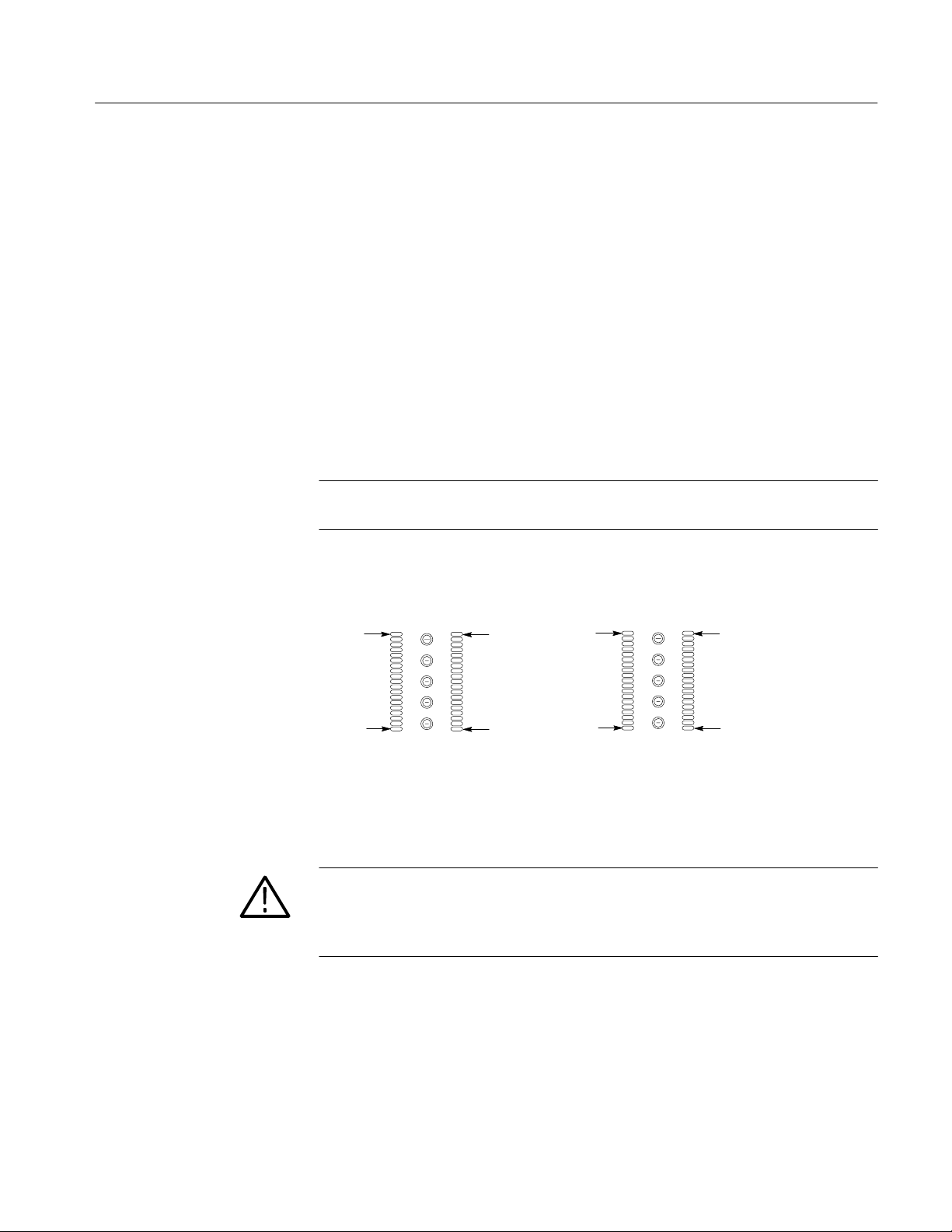
CPU To Mictor Connections
To probe the microprocessor you will need to make connections between the
CPU and the Mictor pins of the P6434 Mass Termination Probe. Refer to the
P6434 Mass Termination Probe manual, Tektronix part number 070-9793-xx, for
more information on mechanical specifications. Table 1–16 through Table 1–20
show the CPU pin to Mictor pin connections.
Tektronix uses a counter-clockwise pin assignment. Pin-1 is located at the top
left, and pin-2 is located directly below it. Pin-20 is located on the bottom right,
and pin-21 is located directly above it.
AMP uses an odd side-even side pin assignment. Pin-1 is located at the top left,
and pin-3 is located directly below it. Pin-2 is located on the top right, and pin-4
is located directly below it.
NOTE. When designing Mictor connectors into your SUT, always follow the
Tektronix pin assignment.
Getting Started
Tektronix Pinout AMP Pinout
Pin 1
Pin 19
Pin 38
Pin 20
Pin 1
Pin 37
Pin 2
Pin 38
Figure 1–1: Pin assignments for a Mictor connector (component side)
Please pay close attention to the caution below.
CAUTION. To protect the CPU and the inputs of the module, it is recommended
that a 180W resistor is connected in series between each ball pad of the CPU and
each pin of the Mictor connector. The resistor must be no farther away from the
ball pad of the CPU than 1/2-inch.
TMS 541 PPC7X0 Microprocessor Support
1–15
Page 30

Getting Started
T able 1–16: TLA 700 CPU to Mictor connections for Mictor A pins
Tektronix
Mictor A
pin number
1 1 NC NC NC
2 3 NC NC NC
3 5 TEA* J1 H13
4 7 A0 A13 C16
5 9 A1 D2 E4
6 11 A2 H11 D13
7 13 A3 C1 F2
8 15 A4 B13 D14
9 17 A5 F2 G1
10 19 A6 C13 D15
11 21 A7 E5 E2
12 23 A8 D13 D16
13 25 A9 G7 D4
14 27 A10 F12 E13
15 29 A11 G3 G2
16 31 A12 G6 E15
17 33 A13 H2 H1
18 35 A14 E2 E16
19 37 A15 L3 H2
20 38 A31 L2 P1
21 36 A30 K2 J15
22 34 A29 K3 M1
23 32 A28 J6 H16
24 30 A27 J2 K2
25 28 A26 H3 G15
26 26 A25 M3 K1
27 24 A24 J7 G13
28 22 A23 F3 F4
29 20 A22 G2 F16
30 18 A21 E1 H3
31 16 A20 H7 F15
32 14 A19 J4 J2
33 12 A18 G4 F14
34 10 A17 L4 J1
35 8 A16 G5 F13
AMP
Mictor A
pin number
PPC7X0 signal name PPC750 PPC740
1–16
TMS 541 PPC7X0 Microprocessor Support
Page 31
Getting Started
T able 1–16: TLA 700 CPU to Mictor connections for Mictor A pins (cont.)
Tektronix
Mictor A
pin number
36 6 TA* F1 H14
37 4 NC NC NC
38 2 NC NC NC
39 39 GND NC NC
40 40 GND NC NC
41 41 GND NC NC
42 42 GND NC NC
43 43 GND NC NC
AMP
Mictor A
pin number
PPC740PPC750 PPC7X0 signal name
T able 1–17: DAS 9200 CPU to LA connections
LA channel PPC7X0 signal name PPC750 PPC740
0_CLK:0 TEA* J1 H13
0_A3:7 A0 A13 C16
0_A3:6 A1 D2 E4
0_A3:5 A2 H11 D13
0_A3:4 A3 C1 F2
0_A3:3 A4 B13 D14
0_A3:2 A5 F2 G1
0_A3:1 A6 C13 D15
0_A3:0 A7 E5 E2
0_A2:7 A8 D13 D16
0_A2:6 A9 G7 D4
0_A2:5 A10 F12 E13
0_A2:4 A11 G3 G2
0_A2:3 A12 G6 E15
0_A2:2 A13 H2 H1
0_A2:1 A14 E2 E16
0_A2:0 A15 L3 H2
0_A0:0 A31 L2 P1
0_A0:1 A30 K2 J15
0_A0:2 A29 K3 M1
0_A0:3 A28 J6 H16
0_A0:4 A27 J2 K2
TMS 541 PPC7X0 Microprocessor Support
1–17
Page 32
Getting Started
T able 1–17: DAS 9200 CPU to LA connections (cont.)
LA channel PPC740PPC750 PPC7X0 signal name
0_A0:5 A26 H3 G15
0_A0:6 A25 M3 K1
0_A0:7 A24 J7 G13
0_A1:0 A23 F3 F4
0_A1:1 A22 G2 F16
0_A1:2 A21 E1 H3
0_A1:3 A20 H7 F15
0_A1:4 A19 J4 J2
0_A1:5 A18 G4 F14
0_A1:6 A17 L4 J1
0_A1:7 A16 G5 F13
0_CLK:1 TA* F1 H14
T able 1–18: TLA 700 CPU to Mictor connections for Mictor C pins
Tektronix
Mictor C
pin number
1 1 NC
2 3 NC NC NC
3 5 CLK H9 C9
4 7 TT3 C12 C14
5 9 TT2 B12 B16
6 11 TEA* J1 H13
7 13 BG* H1 L1
8 15 TSIZ2 C9 B12
9 17 TBST* A11 A14
10 19 TT0 C10 B13
11 21 NC
12 23 TSIZ1 B9 D10
13 25 TSIZ0 A9 A13
14 27 DBB* K5 J14
15 29 ABB* L7 K4
16 31 DRTRY* H6 G16
17 33 TS* K7 J13
18 35 AACK* N3 L2
AMP
Mictor C
pin number
PPC7X0 signal name PPC750 PPC740
NC
NC
NC
NC
1–18
TMS 541 PPC7X0 Microprocessor Support
Page 33

Getting Started
T able 1–18: TLA 700 CPU to Mictor connections for Mictor C pins (cont.)
Tektronix
Mictor C
pin number
19 37 ARTRY_ERLY* L6 J4
20 38 ARTRY_DAT A* L6 J4
21 36 AACK* N3 L2
22 34 TS* K7 J13
23 32 DRTRY* H6 G16
24 30 DBWO* D1 G4
25 28 GBL* B1 F1
26 26 TA* F1 H14
27 24 TT1 D11 A15
28 22 NC NC NC
29 20 HRESET* B6 A7
30 18 TT4 F11 C15
31 16 SYSCLK H9 C9
32 14 DBG* K1 N1
33 12 BR* E7 B6
34 10 ARTRY* L6 J4
35 8 WT C3 D2
36 6 NC NC NC
37 4 NC NC NC
38 2 NC NC NC
39 39 GND NC NC
40 40 GND NC NC
41 41 GND NC NC
42 42 GND NC NC
43 43 GND NC NC
AMP
Mictor C
pin number
PPC740PPC750 PPC7X0 signal name
T able 1–19: DAS 9200 CPU to LA connections
LA channel PPC7X0 signal name PPC750 PPC740
0_CLK:3 CLK H9 C9
0_C3:7 TT3 C12 C14
0_C3:6 TT2 B12 B16
0_C3:5 TEA* J1 H13
0_C3:4 BG* H1 L1
TMS 541 PPC7X0 Microprocessor Support
1–19
Page 34

Getting Started
T able 1–19: DAS 9200 CPU to LA connections (cont.)
LA channel PPC740PPC750 PPC7X0 signal name
0_C3:3 TSIZ2 C9 B12
0_C3:2 TBST* A11 A14
0_C3:1 TT0 C10 B13
0_C2:7 TSIZ1 B9 D10
0_C2:6 TSIZ0 A9 A13
0_C2:5 DBB* K5 J14
0_C2:4 ABB* L7 K4
0_C2:3 DRTRY* H6 G16
0_C2:2 TS* K7 J13
0_C2:1 AACK* N3 L2
0_C2:0 ARTRY_ERLY* L6 J4
1_C2:0 ARTRY_DATA* L6 J4
1_C2:1 AACK* N3 L2
1_C2:2 TS* K7 J13
1_C2:3 DRTRY* H6 G16
1_C2:4 DBWO* D1 G4
1_C2:5 GBL* B1 F1
1_C2:6 TA* F1 H14
1_C2:7 TT1 D11 A15
1_C3:1 HRESET* B6 A9
1_C3:2 TT4 F11 C15
1_C3:3 SYSCLK H9 C9
1_C3:4 DBG* K1 N1
1_C3:5 BR* E7 B6
1_C3:6 ARTRY* L6 J4
1_C3:7 WT C3 D2
1–20
T able 1–20: CPU to Mictor connections for Mictor D pins
Tektronix
Mictor D
pin number
1 1 NC NC NC
2 3 NC NC NC
3 5 NC NC NC
4 7 DL0 M6 K13
AMP
Mictor D
pin number
PPC7X0 signal name PPC750 PPC740
TMS 541 PPC7X0 Microprocessor Support
Page 35

T able 1–20: CPU to Mictor connections for Mictor D pins (cont.)
Getting Started
Tektronix
Mictor D
pin number
5 9 DL1 P3 K15
6 11 DL2 N4 K16
7 13 DL3 N5 L16
8 15 DL4 R3 L15
9 17 DL5 M7 L13
10 19 DL6 T2 L14
11 21 DL7 N6 M16
12 23 DL8 U2 M15
13 25 DL9 N7 M13
14 27 DL10 P11 N16
15 29 DL11 V13 N15
16 31 DL12 U12 N13
17 33 DL13 P12 N14
18 35 DL14 T13 P16
19 37 DL15 W13 P15
20 38 DL31 W2 R4
21 36 DL30 U3 T3
22 34 DL29 V3 P4
23 32 DL28 R2 T2
24 30 DL27 N1 T1
25 28 DL26 U1 R3
26 26 DL25 V1 N4
27 24 DL24 P1 N3
28 22 DL23 T1 P3
29 20 DL22 V8 T13
30 18 DL21 V12 N12
31 16 DL20 U11 P13
32 14 DL19 T11 N10
33 12 DL18 W8 T14
34 10 DL17 V10 R14
35 8 DL16 U13 R16
36 6 DBB* K5 J14
37 4 NC NC NC
38 2 NC NC NC
39 39 GND NC NC
AMP
Mictor D
pin number
PPC740PPC750PPC7X0 signal name
TMS 541 PPC7X0 Microprocessor Support
1–21
Page 36

Getting Started
T able 1–20: CPU to Mictor connections for Mictor D pins (cont.)
Tektronix
Mictor D
pin number
40 40 GND NC NC
41 41 GND NC NC
42 42 GND NC NC
43 43 GND NC NC
AMP
Mictor D
pin number
T able 1–21: CPU to LA connections
LA channel PPC7X0 signal name PPC750 PPC740
0_D3:7 DL0 M6 K13
0_D3:6 DL1 P3 K15
0_D3:5 DL2 N4 K16
0_D3:4 DL3 N5 L16
0_D3:3 DL4 R3 L15
0_D3:2 DL5 M7 L13
0_D3:1 DL6 T2 L14
0_D3:0 DL7 N6 M16
0_D2:7 DL8 U2 M15
0_D2:6 DL9 N7 M13
0_D2:5 DL10 P11 N16
0_D2:4 DL11 V13 N15
0_D2:3 DL12 U12 N13
0_D2:2 DL13 P12 N14
0_D2:1 DL14 T13 P16
0_D2:0 DL15 W13 P15
0_D0:0 DL31 W2 R4
0_D0:1 DL30 U3 T3
0_D0:2 DL29 V3 P4
0_D0:3 DL28 R2 T2
0_D0:4 DL27 N1 T1
0_D0:5 DL26 U1 R3
0_D0:6 DL25 V1 N4
0_D0:7 DL24 P1 N3
0_D1:0 DL23 T1 P3
PPC740PPC750PPC7X0 signal name
1–22
TMS 541 PPC7X0 Microprocessor Support
Page 37

T able 1–21: CPU to LA connections (cont.)
LA channel PPC740PPC750PPC7X0 signal name
0_D1:1 DL22 V8 T13
0_D1:2 DL21 V12 N12
0_D1:3 DL20 U1 1 P13
0_D1:4 DL19 T1 1 N10
0_D1:5 DL18 W8 T14
0_D1:6 DL17 V10 R14
0_D1:7 DL16 U13 R16
0_CLK:2 DBB* K5 J14
T able 1–22: TLA 700 CPU to Mictor connections for Mictor E pins
Getting Started
Tektronix
Mictor E
pin number
1 1 NC NA NA
2 3 NC NA NA
3 5 NC NC NC
4 7 DH0 W12 P14
5 9 DH1 W11 Y16
6 11 DH2 V11 R15
7 13 DH3 T9 T15
8 15 DH4 W10 R13
9 17 DH5 U9 R12
10 19 DH6 U10 P11
11 21 DH7 M11 N11
12 23 DH8 M9 R11
13 25 DH9 P8 T12
14 27 DH10 W7 T11
15 29 DH11 P9 R10
16 31 DH12 W9 P9
17 33 DH13 R10 N9
18 35 DH14 W6 T10
19 37 DH15 V7 V7
20 38 DH31 R5 T4
21 36 DH30 U4 T5
22 34 DH29 W3 N5
AMP
Mictor E
pin number
PPC7X0 signal name PPC750 PPC740
TMS 541 PPC7X0 Microprocessor Support
1–23
Page 38

Getting Started
T able 1–22: (cont.)TLA 700 CPU to Mictor connections for Mictor E pins
Tektronix
Mictor E
pin number
23 32 DH28 V4 R5
24 30 DH27 V5 T6
25 28 DH26 P7 R6
26 26 DH25 W4 N6
27 24 DH24 U5 P6
28 22 DH23 W5 T7
29 20 DH22 U6 R7
30 18 DH21 R7 N7
31 16 DH20 U7 T8
32 14 DH19 T7 R8
33 12 DH18 V9 N8
34 10 DH17 U8 P8
35 8 DH16 V6 T9
36 6 NC
37 4 NC NC NC
38 2 NC NC NC
39 39 GND NC NC
40 40 GND NC NC
41 41 GND NC NC
42 42 GND NC NC
43 43 GND NC NC
AMP
Mictor E
pin number
NC
PPC740PPC750PPC7X0 signal name
NC
1–24
T able 1–23: DAS 9200 CPU to LA connections
LA channel PPC7X0 signal name PPC750 PPC740
1_D3:7 DH0 W12 P14
1_D3:6 DH1 W11 Y16
1_D3:5 DH2 V11 R15
1_D3:4 DH3 T9 T15
1_D3:3 DH4 W10 R13
1_D3:2 DH5 U9 R12
1_D3:1 DH6 U10 P1 1
1_D3:0 DH7 M11 N11
1_D2:7 DH8 M9 R11
TMS 541 PPC7X0 Microprocessor Support
Page 39

T able 1–23: DAS 9200 CPU to LA connections (cont.)
LA channel PPC740PPC750PPC7X0 signal name
1_D2:6 DH9 P8 T12
1_D2:5 DH10 W7 T11
1_D2:4 DH11 P9 R10
1_D2:3 DH12 W9 P9
1_D2:2 DH13 R10 N9
1_D2:1 DH14 W6 T10
1_D2:0 DH15 V7 V7
1_D0:0 DH31 R5 T4
1_D0:1 DH30 U4 T5
1_D0:2 DH29 W3 N5
1_D0:3 DH28 V4 R5
1_D0:4 DH27 V5 T6
1_D0:5 DH26 P7 R6
1_D0:6 DH25 W4 N6
1_D0:7 DH24 U5 P6
1_D1:0 DH23 W5 T7
1_D1:1 DH22 U6 R7
1_D1:2 DH21 R7 N7
1_D1:3 DH20 U7 T8
1_D1:4 DH19 T7 R8
1_D1:5 DH18 V9 N8
1_D1:6 DH17 U8 P8
1_D1:7 DH16 V6 T9
Getting Started
TMS 541 PPC7X0 Microprocessor Support
1–25
Page 40

Getting Started
1–26
TMS 541 PPC7X0 Microprocessor Support
Page 41

Operating Basics
Page 42

Page 43

Setting Up the Support
This section provides information on how to set up the support. Information
covers the following topics:
H Channel group definitions
H Clocking options
H Symbol table files
The information in this section is specific to the operations and functions of the
TMS 541 PPC7X0 support on any Tektronix logic analyzer for which the support
can be purchased. Information on basic operations describes general tasks and
functions.
Before you acquire and display disassemble data, you need to load the support
and specify the setups for clocking and triggering as described in the information
on basic operations. The support provides default values for each of these setups,
but you can change them as needed.
Channel Group Definitions
Clocking
Clocking Options
The software automatically defines channel groups for the support. The channel
groups for the PPC7X0 support are Address, Data, Control, Transfer (Tran), Tsiz,
and Misc. If you want to know which signal is in which group, refer to the
channel assignment tables beginning on page 1–4.
The TMS 541 support offers a microprocessor-specific clocking mode for the
PPC7X0 microprocessor. This clocking mode is the default selection whenever
you load the PPC7X0 support.
Disassembly will not be correct with the Internal or External clocking modes.
Information on basic operations describes how to use these clock selections for
general purpose analysis.
TMS 541 PPC7X0 Microprocessor Support
2–1
Page 44

Setting Up the Support
Custom Clocking
A special clocking program is loaded to the module every time you load the
PPC7X0 support. This special clocking is called Custom.
With Custom clocking, the module logs in signals from multiple channel groups
at different times when the signals are valid on the PPC7X0 bus. The module
then sends all the logged-in signals to the trigger machine and to the acquisition
memory of the module for storage.
In Custom clocking, the module clocking state machine (CSM) generates one
master sample for each microprocessor bus cycle, no matter how many clock
cycles are contained in the bus cycle.
TLA 700. When Custom is selected, the Custom Clocking Options menu will have
the sub-title “PPC7X0 Microprocessor Clocking Support” added, and the
clocking options will also be displayed.
Bus timing diagram. All the data signals D[0–63] are logged in during ’D’ strobe
and DBG* and DBWO* are logged in during ’DBB’ strobe. All the address
signals A[0–31] and the remaining signals are strobed in during ’A’ strobe. See
Figure 2–1.
NOTE. ABB* and BG* logged in by the ’A’ strobe are their states during the
previous cycle.
An ’M’ strobe is done if one or more of the following conditions are met:
TA* is asserted
TS* is asserted
ARTRY* is asserted on the second clock after the assertion of AACK*
DRTRY* is asserted OR
TEA* is asserted
2–2
TMS 541 PPC7X0 Microprocessor Support
Page 45

CLK
BR*
BG*
ABB*
TS*
1 2 3 4 5 6 7 10 11
Setting Up the Support
12
13
A [0:31]
AACK*
ARTRY*
DBG*
DBB*
TA*
D [0:63]
TEA*
DBB DBB AD
DBB
M
Addr Addr Addr
D1 D2 D3 D0 D1
D0
AD
M
DBB ADMADMAD
M
DBBADMADMAD
DBB
M
Figure 2–1: PPC750/PPC740 Bus Timing Diagram
TMS 541 PPC7X0 Microprocessor Support
2–3
Page 46

Setting Up the Support
Symbols
The TMS 541 support supplies three symbol-table file. The PPC7X0_Ctrl file
replaces specific Control-channel group values with symbolic values when
Symbolic is the radix for the channel group.
Symbol tables are generally not for use in timing or PPC7X0_T support
disassembly.
Table 2–1 shows the definitions for name, bit pattern, and meaning of the Control
group symbols in file PPC7X0_Tran.
T able 2–1: PPC7X0_Tran Control group symbol table definitions
Control group value
TT0 TT2
Symbol
FETCH
DA TA_READ
DA TA_WRT
ADDR_ONLY
UNKNOWN
TT1 TT3
X1 X1X1
X1 X1X0
X0 X1XX
XX X0XX
XX XXXX
TT4
WT
Description
Instruction fetch cycle
Read cycle
Write cycle
Address only cycle
Unknown transfer cycle
Table 2–2 shows the definitions for name, bit pattern, and meaning of the Control
group symbols in file PPC7X0_Tsiz.
T able 2–2: PPC7X0_Tsiz Control group symbol table definitions
Control group value
TSIZ0
TSIZ1
Symbol
BURST
8_BYTE
1_BYTE
2_BYTE
3_BYTE
4_BYTE
5_BYTE
6_BYTE
TSIZ2
TBST*
0100
0001
0011
0101
0111
1001
1011
1101
Description
Burst transaction
Single beat 8-Byte transaction
Single beat 1-Byte transaction
Single beat 2-Byte transaction
Single beat 3-Byte transaction
Single beat 4-Byte transaction
Single beat 5-Byte transaction
Single beat 6-Byte transaction
2–4
TMS 541 PPC7X0 Microprocessor Support
Page 47

T able 2–2: PPC7X0_Tsiz Control group symbol table definitions (cont.)
Control group value
TSIZ0
TSIZ1
Symbol Description
7_BYTE
UNKNOWN
TSIZ2
1111
XXXX
Table 2–3 shows the definitions for name, bit pattern, and meaning of the Control
group symbols in file PPC7X0_Ctrl.
T able 2–3: PPC7X0_Ctrl Control group symbol table definitions
Control group value
TS* DRTRY* ABB*
BG* AACK* DBWO*
Symbol
ART_P0E
ART_P1E
ART_DRT
ART_P0D
ART_P1D
P0A_P0E
P0A_P1E
P1A_P0E
P1A_P1E
P0A_DRT
P1A_DRT
P0A_P0D
P0A_P1D
P1A_P0D
P1A_P1D
P0_A
P1_A
P0_E
P1_E
DRT
P0_D
DBG* TA* DBB*
ARTRY* TEA*
XX00 XXX0 XXX
XXX0 XXX0 XXX
XXX0 0XXX XXX
XX00 XX0X XXX
XXX0 XX0X XXX
0001 XXX0 XXX
00X1 XXX0 XXX
0X01 XXX0 XXX
0XX1 XXX0 XXX
00X1 0XXX XXX
0XX1 0XXX XXX
0001 XX0X XXX
00X1 XX0X XXX
0X01 XX0X XXX
0XX1 XX0X XXX
00X1 XXXX XXX
0XX1 XXXX XXX
XX0X XXX0 XXX
XXXX XXX0 XXX
XXXX 0XXX XXX
XX0X XX0X XXX
Setting Up the Support
TBST*
Single beat 7-Byte transaction
Unknown tsiz cycle
Description
ARTRY cycle and PPC0’s Data Error
ARTRY cycle and PPC1’s Data Error
ARTRY cycle and Data retry
ARTRY cycle and PPC0’s Data
ARTRY cycle and PPC1’s Data
PPC0 Address and PPC0’s Data Error
PPC0 Address and PPC1’s Data Error
PPC1 Address and PPC0’s Data Error
PPC1 Address and PPC1’s Data Error
PPC0 Address and Data retry
PPC1 Address and Data retry
PPC0 Address and Data
PPC0 Address and PPC1’s Data
PPC1 Address and PPC0’s Data
PPC1 Address and Data
PPC0 Address cycle
PPC1 Address cycle
PPC0 Data Error
PPC1 Data Error
DRTRY cycle
PPC0 Data cycle
TMS 541 PPC7X0 Microprocessor Support
2–5
Page 48

Setting Up the Support
T able 2–3: PPC7X0_Ctrl Control group symbol table definitions (cont.)
Control group value
TS* DRTRY* ABB*
BG* AACK* DBWO*
Symbol Description
P1_D
ART
UNKNOWN
DBG* TA* DBB*
ARTRY* TEA*
PPC1 Data cycle
ARTRY cycle
Unknown cycle
Information on basic operations describes how to use symbolic values for
triggering and for displaying other channel groups symbolically, such as for the
Address channel group.
2–6
TMS 541 PPC7X0 Microprocessor Support
Page 49

Acquiring and Viewing Disassembled Data
This section describes how to acquire data and view it disassembled. Information
covers the following topics and tasks:
H Acquiring data
H Viewing disassembled data in various display formats
H Cycle type labels
H Changing the way data is displayed
H Changing disassembled cycles with the mark cycles function
Acquiring Data
Once you load the PPC7X0 support, choose a clocking mode, and specify the
trigger, you are ready to acquire and disassemble
If you have any problems acquiring data, refer to information on basic operations
in your online help or Appendix A: Error Messages and Disassembly Pr oblems in
the basic operations user manual.
data.
Viewing Disassembled Data
You can view disassembled data in four display formats: Hardware, Software,
Control Flow, and Subroutine. The information on basic operations describes
how to select the disassembly display formats.
NOTE. Selections in the Disassembly property page (the Disassembly Format
Definition overlay) must be set correctly for your acquired data to be disassembled correctly. Refer to Changing How Data is Displayed on page 2–11.
The default display format shows the Address, HI_Data, LO_Data, Control,
Transfer and Tsiz channel group values for each sample of acquired data.
If a channel group is not visible, you must use the Disassembly property page to
make the group visible.
The disassembler displays special characters and strings in the instruction
mnemonics to indicate significant events. Table 2–4 shows these special
characters and strings, and gives a definition of what they represent.
TMS 541 PPC7X0 Microprocessor Support
2–7
Page 50
Acquiring and Viewing Disassembled Data
T able 2–4:
Character or string displayed Description
>> On the TLA 700
m On the DAS 9200
****
#
-ā-ā-ā-ā-ā-ā-ā-
-ā-ā-ā-ā-ā-ā-ā-
-ā-ā-ā-ā-ā-ā-ā-
-ā-
-ā-ā-ā-ā-ā-ā-ā-
Description of special characters in the display
The instruction was manually marked
Indicates there is insufficient data available for complete
disassembly of the instruction; the number of asterisks
indicates the width of the data that is unavailable. Each two
asterisks represent one byte.
Indicates an immediate value
In the Address channel group, this indicates that the
sequence did not have information that could be disassembled
In the HI_Data and LO_Data groups, this indicates that the
sequence does not contain valid data
In the LO_Data group, indicates that the bus configuration is
32-Bits
In the invalidate byte lanes, this indicates a Data Read or
Data Write transaction
Indicates a flushed instruction when only one of the
instructions fetched is executed
Hardware Display Format
<Hex value>
In whole bytes that are not valid, indicates invalidated data;
the value for invalidated data is hexcadecimal
In Hardware display format, the disassembler displays certain cycle type labels in
parentheses.
If a single sequence has both an Address/Direct Store Access cycle and a Data
cycle, then a combination of cycle type labels described in Tables 2–5, 2–6, and
2–7 is displayed. For example, if Alternate Master Address and Alternate Master
Data are acquired in one sample, the disassembler would display the cycle type
label ( ALT ADDRS AND ALT DATA ).
T able 2–5: Cycle type labels for Address sequences and definitions
Cycle type Definition
( PPC_ADDRS )
( PPC_ART_ADDRS )
( ALT_ADDRS )
( INCOM_ADDRS )
Address cycle with selected processor mastership
Selected processor Address retried
Alternate master address
Invalid selected processor Address which cannot associate with
any data
2–8
TMS 541 PPC7X0 Microprocessor Support
Page 51

Acquiring and Viewing Disassembled Data
T able 2–6: Cycle type labels for Data sequences and definitions
Cycle type label Definition
( PPC_DATA ) Data cycle with selected processor mastership
( ALT_DATA ) Alternate Master Data
( PPC_DRT_DA TA ) Selected Processor data retried
( INCOM_DATA ) Invalid selected processor Data does not associate with it’s
address.
T able 2–7: Cycle type labels for ARTRY, DRTRY, and Data Error cycles
Cycle type label Definition
( DATA_RETRY ) Sequence having DRTRY* assertion
( PPC_DATA_ERR ) Data error in selected processor data – Assertion of TEA
( ALT_DATA_ERR ) Data error in Alternate Master Data
( ARTRY_CYCLE ) Sequence having ARTRY* asserted
( **BAD CYCLE TYPE** ) Cycle does not carry valid information
T able 2–8: General cycle type labels definitions
Cycle type label Definition
( FLUSH ) An instruction is fetched but not executed, it is labeled as FLUSH
( FLUSH: PREDICTION FAIL ) An instruction that was fetched based on the prediction bit, but
the prediction was incorrect
( CACHE FILL ) Burst read transfer that occurs after wrap around of the end of
the cache line
( CLEAN BlOCK ) Clean Block transaction
( FLUSH BlOCK ) Flush Block transaction
( SYNC ) Address Only transaction due to the execution of Sync instruction
( KILL BLOCK ) Kill Block transaction
( EIEIO ) Enforce In-Order Execution of I/O cycle
( EXT CTR WD WRT ) External Control Word Write transaction
( EXT CTR WD RD ) External Control Word Read transaction
( WRT WITH FLUSH ) Write-with-Flush operation issued by the processor
( WRT WITH KILL ) Write with Kill operation
( DATA READ ) Single Beat Read or Burst Read operation
TMS 541 PPC7X0 Microprocessor Support
2–9
Page 52

Acquiring and Viewing Disassembled Data
T able 2–8: General cycle type labels definitions (cont.)
Cycle type label Definition
( RWITM ) Read-With-Intent-To-Modify transaction
( WWF-AT OMIC ) Write-With-Flush-Atomic operations issued by the processor
( READ-AT OMIC ) Read-Atomic operation
( RWITM-ATOMIC ) Read-With-Intent-T o-Modify-Atomic transaction
( RESERVED ) Reserved Transaction type match any of the defined patterns
Software Display Format
Control Flow Display
Format
2–10
Figure 2–2: Example of the hardware display format
The Software display format shows only the first fetch of executed instructions.
Flushed cycles and extensions are not shown, even though they are part of the
executed instruction. Data reads and writes are not displayed.
The Control Flow display format shows only the first fetch of instructions that
change the flow of control.
TMS 541 PPC7X0 Microprocessor Support
Page 53

Acquiring and Viewing Disassembled Data
Instructions that generate a change in the flow of control in the PPC7X0
microprocessor are as follows:
bblsc
ba bla rfi
Instructions that might generate a change in the flow of control in the PPC7X0
microprocessor are as follows:
bc bcla bcctr tdi
bca bclr bcctrl tw
bcl bclrl td twi
The disassembler displays some instructions that cause traps or interrupts, as well
as exception vector reads that are taken and the message" ( **BAD CYCLE
TYPE** ). Mnemonics misinterpreted by the disassembler are also displayed.
Subroutine Display
Format
The Subroutine display format shows only the first fetch of subroutine call and
return instructions. It will display conditional subroutine calls if they are
considered to be taken.
Instructions that generate a subroutine call or a return in the PPC7X0 microprocessor are as follows:
sc rfi
Instructions that might generate a subroutine call or a return in the PPC7X0
microprocessor are as follows:
td tdi tw twi
The disassembler displays some instructions that cause traps or interrupts, as well
as exception vector reads that are taken and the message" ( **BAD CYCLE
TYPE** ). Mnemonics misinterpreted by the disassembler are also displayed.
Changing How Data is Displayed
There are common fields and features that allow you to further modify displayed
data to suit your needs. You can make common and optional display selections in
the Disassembly property page (the Disassembly Format Definition overlay).
You can make selections unique to the PPC7X0 support to do the following
tasks:
H Change how data is displayed across all display formats
H Change the interpretation of disassembled cycles
TMS 541 PPC7X0 Microprocessor Support
2–11
Page 54

Acquiring and Viewing Disassembled Data
H Display exception cycles
Optional Display
Selections
You can make optional selections for disassembled
common selections (described in the information on basic operations), you can
change the displayed data in the following ways:
H Select a bus configuration and the trace PPC7X0 microprocessor
H Select the prefetch byte order
H Select the alternate byte order low and high bounds
H Select the exception byte order
H Specify the exception prefix
The PPC7X0 microprocessor support product has six additional fields: Bus
Processor Select, Prefetch Byte Ord, Alt-Byte Ord-Lo Bound, Alt-Byte Ord-Hi
Bound, Exception Byte Ord, and Exception Prefix. These fields appear in the
area indicated in the basic operations user manual.
Proc Select. You can select which PPC7X0 microprocessor to trace: PPC0 or
PPC1. The microprocessor from which the BG* and DBG* signals are acquired
are considered PPC0 and all others are PPC1s.
Prefetch Byte Order. You can select the byte ordering for the predominant
instruction fetches as Big- or Little-Endian.
data. In addition to the
2–12
Alt Byte Ord - Lo Bound and Alt Byte Ord - Hi Bound. You can enter the low and
high bounds for the alternate byte ordering range. The default is 00000000.
You should enter alternate values on double-word boundaries. If the value is not
on a double-word boundary, the disassembler assumes the value to be the nearest
double-word.
If you do not enter a value in the field, the data is acquired and disassembled
according to the selection in the Prefetch Byte Ord field.
NOTE. The alternate high bound value must be greater than the alternate low
bound value or disassembly will be incorrect.
Exception Byte Order. You can select the byte ordering for exception processing
as Big- or Little-Endian.
TMS 541 PPC7X0 Microprocessor Support
Page 55

Acquiring and Viewing Disassembled Data
Exception Prefix. You can enter the prefix value of the exception table as 000 to
FFF. The default prefix value is FFF. The exception table must reside in external
memory for interrupt and exception cycles to be visible to the disassembler.
NOTE. If an address is in the Exception processing region and in the range
selected for the alternate byte ordering, the disassembler uses the byte ordering
selected for the Exception processing.
Marking Cycles
The disassembler has a Mark Opcode function that allows you to change the
interpretation of a cycle type. Using this function, you can select a cycle and
change it.
TLA 700. Marks are placed by using the Mark Opcode button. The Mark Opcode
button will always be available. If the sample being marked is not an Address
cycle or Data cycle of the potential bus master, the Mark Opcode selections will
be replaced by a note indicating that “An Opcode Mark cannot be placed at the
selected data sample.”
When a cycle is marked, the character “>>” is displayed immediately to the left
of the Mnemonics column. Cycles can be unmarked by using the “Undo Mark”
selection, which will remove the character “>>”.
DAS 9200. Marks are placed by using the F4: Mark Data function key. The Mark
Data function key will always be available. If the cursor is not on an Address
cycle or Data cycle of the potenital bus master, then no microprocessor cycle
marks will be available when the key is pressed.
The list of selections varies depending on the selection in the Bus Processor
Select field in the Disassembly property page (Disassembly Format Definition
overlay).
Mark selections available on data sequences without an address and data cycle
associated with a fetch cycle when the PPC7X0 microprocessor is operating in
64-bit mode are as follows:
Opcode - Opcode
Opcode - Flush
Flush - Opcode
Flush - Flush
Incom_Data
Undo Mark
Mark selections available on sequences with only an Address cycle are as
follows:
TMS 541 PPC7X0 Microprocessor Support
2–13
Page 56

Acquiring and Viewing Disassembled Data
Incom_Address
Undo Mark
Mark selections available on sequences with both data and address cycles (if the
data cycle is associated with a fetch cycle) and the PPC7X0 microprocessor is
operating in 64-bit mode are as follows:
Opcode - Opcode
Opcode - Flush
Flush - Opcode
Flush - Flush
Incom_Data
Incom_Address
Opcode - Opcode Incom_Addrs
Opcode - Flush Incom_Addrs
Flush - Opcode Incom_Addrs
Flush - Flush Incom_Addrs
Incom_Addrs Incom_Data
Undo Mark
Mark selections available on sequences with data that is not associated with a
Fetch cycle are as follows:
Incom_Data
Undo Mark
Table 2–9 describes the various combinations of mark selections.
T able 2–9: Mark selections and definitions
Mark selection or combination[
Opcode - Opcode
Opcode - Flush
Flush - Opcode
Flush - Flush Instructions not disassembled and labeled as ( FLUSH )
Incom_Addrs Valid PPC7X0 address is invalidated and labeled as ( Incom_Addrs )
Opcode - Opcode Incom_Addrs
Opcode - Flush Incom_Addrs
Definition
HI_Data and LO_Data are disassembled
Only HI_Data is disassembled in Big-Endian mode or only LO_Data is disassembled in
Little-Endian mode
Only LO_Data is disassembled in Big-Endian mode or only HI_Data is disassembled in
Little-Endian mode
Use to mark a sequence with PPC7X0 address and data from different transactions;
HI_Data and LO_Data are disassembled; the address is invalidated
HI_Data is disassembled only in Big-Endian mode or LO_Data is disassembled only in
Little-Endian mode; the address is invalidated
Flush - Opcode Incom_Addrs
Flush - Flush Incom_Addrs Instructions not disassembled and labeled as ( FLUSH ); the address is invalidated
2–14
LO_Data is disassembled only in Big-Endian mode or HI_Data is disassembled only in
Little-Endian mode; the address is invalidated
TMS 541 PPC7X0 Microprocessor Support
Page 57

T able 2–9: Mark selections and definitions (cont.)
Acquiring and Viewing Disassembled Data
Mark selection or combination[
Incom_Addrs
Incom_Data
Incom_Addrs Incom_Data
Undo Mark
[ Mark selections intended to be used on sequences with data are not available for non-instructions.
Definition
Address is invalidated
HI_Data and LO_Data are invalidated
Address, HI_Data, and LO_Data are invalidated
Removes all marks
The Incom_Addrs mark invalidates the address from being associated with the
wrong data. You can use this mark if you determine that the data for the address
was not acquired.
The Incom_Data mark invalidates the data from being associated with the wrong
address. You can use this mark if you determine that the address for the data was
not acquired.
Information on basic operations contains more details on marking cycles.
Displaying Exception
Labels
The disassembler can display PPC7X0 exception labels. The exception table
must reside in external memory for interrupt and exception cycles to be visible to
the disassembler.
You can enter the table prefix in the Exception Prefix field. The Exception Prefix
field provides the disassembler with the offset address; enter a three-digit
hexadecimal value corresponding to the prefix of the exception table.
These fields are located in the Disassembly property page (Disassembly Format
Definition overlay).
Table 2–10 lists the PPC7X0 interrupt and exception labels.
T able 2–10: Interrupt and exception labels
Offset Displayed interrupt or exception name
0x00000 ( RESERVED )
0x00100 ( SYSTEM RESET )
0x00200 ( MACHINE CHECK EXPN )
0x00300 ( DSI EXPN)
0x00400 ( ISI EXPN)
0x00500 ( EXTERNAL INTRPT )
0x00600 ( ALIGNMENT EXPN )
0x00700 ( PROGRAM EXPN )
TMS 541 PPC7X0 Microprocessor Support
2–15
Page 58
Acquiring and Viewing Disassembled Data
T able 2–10: Interrupt and exception labels (cont.)
Offset Displayed interrupt or exception name
0x00800 ( FLOATING-POINT UNAVLBL EXPN )
0x00900 ( DECREMENTER EXPN )
0x00A00 ( RESERVED )
0x00B00 ( RESERVED )
0x00C00 ( SYSTEM CALL )
0x00D00 ( TRACE EXPN )
0x00E00 ( RESERVED )
0x00F00 ( PERFORMANCE MONITOR EXPN )
0x01000 ( RESERVED )
0x01 100 ( RESERVED )
0x01200 ( RESERVED )
0x01300 ( INST ADDRESS BREAKPOINT EXPN )
0x01400 ( SYS MGMT INTERRUPT EXPN )
0x01500 to 0X16FF ( RESERVED )
0x01700 ( THERMAL MGMT INTRPT )
0x018FF to 0x02FFF ( RESERVED )
Disassembly Display Options
T able 2–11: TLA 700 disassembly display options
Description Option
Show: Hardware Default
Highlight: Software (Default)
Disasm Across Gaps: Yes (Default)
Software
Control Flow
Subroutine
Control Flow
Subroutine
None
No
2–16
TMS 541 PPC7X0 Microprocessor Support
Page 59

Acquiring and Viewing Disassembled Data
T able 2–12: DAS 9200 disassembly display options
Description Option
Display Mode: Hardware Default
Software
Control Flow
Subroutine
Timestamp: Relative Default
Delta
Absolute
Off
Highlight: All
Instructions Default
Control Flow
Subroutines
Highlight Gaps: Y es (Default)
No
Disassemble Across Gaps: Yes
No (Default)
Micro Specific Fields
Prefetch Byte Ordering. Byte ordering for the Predominant Instruction Fetches is
selected by selecting one of the two available options.
Prefetch Byte Ord: Big Endian (default)
Lit Endian
Alternate Byte ordering range is supplied by entering the proper 32 bit Hexadecimal values in the fill-in fields:
Alt Byte Ord – Lo Bound 00000000 (default)
Alt Byte Ord – Hi Bound 00000000 (default)
H Hi Bound Value must be greater than Lo Bound Value, otherwise an
erroneous display may result.
H Values entered are preferred on Double word boundary – if any other value is
entered, it defaults to the nearest double word value. If nothing is entered in
these fields, then the byte ordering that is selected under Prefetch Byte
ordering is assumed for the entire acquisition.
H The range supplied for alternate byte ordering, which is the byte ordering
opposite to that selected for Prefetch Byte Ordering, is assumed.
TMS 541 PPC7X0 Microprocessor Support
2–17
Page 60

Acquiring and Viewing Disassembled Data
Exception Byte Ordering. Byte ordering selected for Exception processing must be
selected by selecting one of the two options.
Exception Byte Ord: Big Endian (default)
Exception Prefix. Valid Exception Prefix is selected by the you by selecting one of
the following two options depending on the system he has used.
Exception Prefix : FFF (default)
000
If an address happens to be in both Exception processing region of the processor
and in the range selected for the alternate byte ordering, then the byte ordering
will be assumed for that address.
Viewing an Example of Disassembled Data
Lit Endian
A demonstration system file (or demonstration reference memory) is provided so
you can see an example of how your PPC7X0 microprocessor bus cycles and
instruction mnemonics look when they are disassembled. Viewing the system file
is not a requirement for preparing the module for use and you can view it without
connecting the logic analyzer to your SUT.
Information on basic operations describes how to view the file.
2–18
TMS 541 PPC7X0 Microprocessor Support
Page 61

Specifications
Page 62

Page 63

Specifications
Specification Tables
This chapter contains information regarding the specifications of the support.
Table 3–1 lists the electrical requirements the SUT must produce for the support
to acquire correct data.
T able 3–1: Electrical specifications
Characteristics Requirements
SUT clock rate
PPC7X0 specified clock rate Max 83.3 MHz
PPC7X0 tested clock rate Max 66 MHz
Minimum setup time required
TLA 700 2.5 ns
DAS 9200 5 ns
Minimum hold time required
TLA 700 0 ns
DAS 9200 0 ns
TMS 541 PPC7X0 Microprocessor Support
3–1
Page 64

Specifications
3–2
TMS 541 PPC7X0 Microprocessor Support
Page 65

Replaceable Parts List
Page 66

Page 67

Replaceable Parts
This section contains a list of the replaceable parts for the TMS 541 PPC7X0
microprocessor support product.
Parts Ordering Information
Replacement parts are available through your local Tektronix field office or
representative.
Changes to Tektronix products are sometimes made to accommodate improved
components as they become available and to give you the benefit of the latest
improvements. Therefore, when ordering parts, it is important to include the
following information in your order.
H Part number
H Instrument type or model number
H Instrument serial number
H Instrument modification number, if applicable
Abbreviations
Mfr. Code to Manufacturer
Cross Index
If you order a part that has been replaced with a different or improved part, your
local Tektronix field office or representative will contact you concerning any
change in part number.
Abbreviations conform to American National Standard ANSI Y1.1–1972.
The table titled Manufacturers Cross Index shows codes, names, and addresses
of manufacturers or vendors of components listed in the parts list.
TMS 541 PPC7X0 Microprocessor Support
4–1
Page 68

Replaceable Parts
Manufacturers cross index
Mfr.
code
80009 TEKTRONIX INC 14150 SW KARL BRAUN DR
Manufacturer Address City , state, zip code
PO BOX 500
Replaceable parts list
Fig. &
index
number
Tektronix
part number
071–0179–01 1 MANUAL,TECH INSTRUC-
070–9802–00 1 MANUAL,TECH USER, BASIC OPERATIONS OF
070–9775–02 1 MANUAL,TECH USER, BASIC OPERATIONS OF
Serial no.
effective
Serial no.
discont’d
Qty Name & description Mfr. code Mfr. part number
STANDARD ACCESSORIES
TIONS,PPC750/740;TMS541
OPTIONAL ACCESSORIES
MICROPROCESSOR SUPPORT ON DAS OR
TLA 500, LOGIC ANALYZER
MICROPROCESSOR SUPPORT ON TLA 700, LOGIC
ANALYZER
BEAVERT ON, OR 97077–0001
80009 071–0179–01
80009 070–9802–00
80009 070–9775–02
4–2
TMS 541 PPC7X0 Microprocessor Support
Page 69

Index
Page 70

Page 71

Index
A
about this manual set, ix
acquiring data, 2–7
Address group, channel assignments, 1–4, 1–5
Address Pipelining, 1–3
address pipelining, 1–3
Alt Byte Ord - Hi Bound field, 2–12
Alt Byte Ord - Lo Bound field, 2–12
Alternate bus master, 1–3
application, logic analyzer configuration, 1–1
B
basic operations, where to find information, ix
Big-Endian byte order, 2–12
bus cycles
AR TRY, DRTRY, and Data Error, 2–9
Data cycle types, 2–9
displayed cycle types, 2–8
displayed general cycle types, 2–9
C
channel assignments
Address group, 1–4, 1–5
clocks, 1–14
Control group, 1–11
Data group, 1–6, 1–7, 1–9, 1–10
DataSize group, 1–12, 1–13
Misc group, 1–13
channel groups, 2–1
visibility , 2–7
clock channel assignments, 1–14
clock rate, 1–2
SUT, 3–1
clocking, Custom, 2–1
how data is acquired, 2–2
connections, CPU to Mictor, 1–15
contacting T ektronix, x
Control Flow display format, 2–10
Control group
channel assignments, 1–11
symbol table, 2–4, 2–5
CPU to Mictor connections, 1–15
Custom clocking, 2–1
how data is acquired, 2–2
cycle types, 2–8
AR TRY, 2–9
combined labels, 2–8
Data, 2–9
Data Error, 2–9
DR TRY, 2–9
general, 2–9
D
data
acquiring, 2–7
disassembly formats
Control Flow, 2–10
Hardware, 2–8
Software, 2–10
Subroutine, 2–11
data cache, 1–2
data display , changing, 2–11
Data group, channel assignments, 1–6, 1–7, 1–9, 1–10
DataSize group, channel assignments, 1–12, 1–13
definitions
disassembler, ix
HI module, x
information on basic operations, ix
LO module, x
logic analyzer, x
module, x
P54C, ix
SUT, ix
XXX, ix
demonstration file, 2–18
disassembled data
AR TRY, DRTRY, and Data Error cycle types, 2–9
cycle type definitions, 2–8
Data cycle types, 2–9
general cycle type definitions, 2–9
viewing, 2–7
viewing an example, 2–18
disassembler
definition, ix
logic analyzer configuration, 1–1
setup, 2–1
Disassembly Format Definition overlay, 2–12
Disassembly property page, 2–12
display formats
Control Flow, 2–10
Hardware, 2–8
Software, 2–10
special characters, 2–7
Subroutine, 2–11
TMS 541 PPC7X0 Microprocessor Support
Index–1
Page 72

Index
E
electrical specifications, 3–1
clock rate, 3–1
Exception Byte Ord field, 2–12
Exception Byte Ordering, 2–18
exception labels, 2–15
Exception Prefix, 2–18
Exception Prefix field, 2–13
Extra Acquisition Channels, 1–3
F
functionality not supported, 1–3
interrupt signals, 1–3
H
Hardware display format, 2–8
AR TRY, DRTRY, and Data Error cycle types, 2–9
cycle type definitions, 2–8
Data cycle types, 2–9
general cycle type definitions, 2–9
HI module, definition, x
hold time, minimum, 3–1
Mark Opcode function, 2–13
marking cycles, definition of, 2–13
Micro Specific Fields
Exception Byte Ordering, 2–18
Exception Prefix, 2–18
Prefetch Byte Ordering, 2–17
Microprocessor, 1–3
microprocessor, specific clocking and how data is
acquired, 2–2
Mictor to CPU connections, 1–15
Misc group, channel assignments, 1–13
module, definition, x
MTIF probes, 1–3
P
P54C, definition, ix
pipelining address, 1–3
Prefetch Byte Ord field, 2–12
Prefetch Byte Ordering, 2–17
R
reference memory, 2–18
Reset, SUT hardware, 1–1
restrictions, 1–1
I
Instruction Cache, 1–2
interrupt signals, functionality not supported, 1–3
L
L2 Cache, 1–3
Little-Endian byte order, 2–12
LO module, definition, x
logic analyzer
configuration for disassembler, 1–1
configuration for the application, 1–1
with a DAS 9200 series, 1–1
with a TLA 700 series, 1–1
definition, x
software compatibility, 1–1
M
manual
conventions, ix
how to use the set, ix
Mark Cycle function, 2–13
S
set up time, minimum, 3–1
setups
disassembler, 2–1
support, 2–1
signals, active low sign, x
Software display format, 2–10
special characters displayed, 2–7
specifications
channel assignments, 1–4
electrical, 3–1
Subroutine display format, 2–11
support, setup, 2–1
support setup, 2–1
SUT, definition, ix
SUT hardware Reset, 1–1
symbol table, Control channel group, 2–4, 2–5
system file, demonstration, 2–18
T
T ektronix, how to contact, x
Index–2
TMS 541 PPC7X0 Microprocessor Support
Page 73

Index
terminology, ix
Timing Display Format, 1–2
Timing Violation, 1–2
V
viewing disassembled data, 2–7
X
XXX, definition, ix
AR TRY, DRTRY, and Data Error, 2–9
TMS 541 PPC7X0 Microprocessor Support
Index–3
Page 74

Index
Index–4
TMS 541 PPC7X0 Microprocessor Support
 Loading...