

Page 1

Instruction Manual
TMS 532
PPC405GP Microprocessor Support
071-0892-00
www.tektronix.com
Page 2

Copyright © T ektronix, Inc. All rights reserved. Licensed software products are owned by Tektronix or its suppliers and
are protected by United States copyright laws and international treaty provisions.
Use, duplication, or disclosure by the Government is subject to restrictions as set forth in subparagraph (c)(1)(ii) of the
Rights in T echnical Data and Computer Software clause at DFARS 252.227-7013, or subparagraphs (c)(1) and (2) of the
Commercial Computer Software – Restricted Rights clause at F AR 52.227-19, as applicable.
T ektronix products are covered by U.S. and foreign patents, issued and pending. Information in this publication supercedes
that in all previously published material. Specifications and price change privileges reserved.
T ektronix, Inc., P.O. Box 500, Beaverton, OR 97077
TEKTRONIX and TEK are registered trademarks of T ektronix, Inc.
Page 3

SOFTWARE WARRANTY
T ektronix warrants that the media on which this software product is furnished and the encoding of the programs on
the media will be free from defects in materials and workmanship for a period of three (3) months from the date of
shipment. If a medium or encoding proves defective during the warranty period, T ektronix will provide a
replacement in exchange for the defective medium. Except as to the media on which this software product is
furnished, this software product is provided “as is” without warranty of any kind, either express or implied.
T ektronix does not warrant that the functions contained in this software product will meet Customer’s
requirements or that the operation of the programs will be uninterrupted or error-free.
In order to obtain service under this warranty, Customer must notify Tektronix of the defect before the expiration
of the warranty period. If T ektronix is unable to provide a replacement that is free from defects in materials and
workmanship within a reasonable time thereafter, Customer may terminate the license for this software product
and return this software product and any associated materials for credit or refund.
THIS WARRANTY IS GIVEN BY TEKTRONIX IN LIEU OF ANY OTHER WARRANTIES, EXPRESS
OR IMPLIED. TEKTRONIX AND ITS VENDORS DISCLAIM ANY IMPLIED WARRANTIES OF
MERCHANTABILITY OR FITNESS FOR A PARTICULAR PURPOSE. TEKTRONIX’
RESPONSIBILITY TO REPLACE DEFECTIVE MEDIA OR REFUND CUSTOMER’S PAYMENT IS
THE SOLE AND EXCLUSIVE REMEDY PROVIDED TO THE CUSTOMER FOR BREACH OF THIS
WARRANTY. TEKTRONIX AND ITS VENDORS WILL NOT BE LIABLE FOR ANY INDIRECT,
SPECIAL, INCIDENTAL, OR CONSEQUENTIAL DAMAGES IRRESPECTIVE OF WHETHER
TEKTRONIX OR THE VENDOR HAS ADVANCE NOTICE OF THE POSSIBILITY OF SUCH
DAMAGES.
Page 4

Table of Contents
Getting Started
Operating Basics
General Safety Summary v. . . . . . . . . . . . . . . . . . . . . . . . . . . . . . . . . . . .
Preface vii. . . . . . . . . . . . . . . . . . . . . . . . . . . . . . . . . . . . . . . . . . . . . . . . . . .
Manual Conventions vii. . . . . . . . . . . . . . . . . . . . . . . . . . . . . . . . . . . . . . . . . . . . . .
Contacting T ektronix viii. . . . . . . . . . . . . . . . . . . . . . . . . . . . . . . . . . . . . . . . . . . . . .
Support Package Description 1–1. . . . . . . . . . . . . . . . . . . . . . . . . . . . . . . . . . . . . . . .
Logic Analyzer Software Compatibility 1–1. . . . . . . . . . . . . . . . . . . . . . . . . . . . . . .
Logic Analyzer Configuration 1–1. . . . . . . . . . . . . . . . . . . . . . . . . . . . . . . . . . . . . . .
Requirements and Restrictions 1–2. . . . . . . . . . . . . . . . . . . . . . . . . . . . . . . . . . . . . . .
Functionality Not T ested 1–2. . . . . . . . . . . . . . . . . . . . . . . . . . . . . . . . . . . . . . . . . . .
Functionality Not Supported 1–2. . . . . . . . . . . . . . . . . . . . . . . . . . . . . . . . . . . . . . . .
Standard Accessories 1–3. . . . . . . . . . . . . . . . . . . . . . . . . . . . . . . . . . . . . . . . . . . . . .
Options 1–3. . . . . . . . . . . . . . . . . . . . . . . . . . . . . . . . . . . . . . . . . . . . . . . . . . . . . . . . .
Connecting the Logic Analyzer to a System Under T est 1–4. . . . . . . . . . . . . . . . . . .
Setting Up the Support 2–1. . . . . . . . . . . . . . . . . . . . . . . . . . . . . . . . . . . . . .
Installing the Support Software 2–1. . . . . . . . . . . . . . . . . . . . . . . . . . . . . . . . . . . . . .
Channel Group Definitions 2–2. . . . . . . . . . . . . . . . . . . . . . . . . . . . . . . . . . . . . . . . .
Support Package Setups 2–3. . . . . . . . . . . . . . . . . . . . . . . . . . . . . . . . . . . . . . . . . . . .
Clocking 2–4. . . . . . . . . . . . . . . . . . . . . . . . . . . . . . . . . . . . . . . . . . . . . . . . . . . . . . . .
Acquiring and Viewing Disassembled Data 2–7. . . . . . . . . . . . . . . . . . . . .
Acquiring Data 2–7. . . . . . . . . . . . . . . . . . . . . . . . . . . . . . . . . . . . . . . . . . . . . . . . . . .
Viewing Disassembled Data 2–7. . . . . . . . . . . . . . . . . . . . . . . . . . . . . . . . . . . . . . . .
Timing Display Format 2–8. . . . . . . . . . . . . . . . . . . . . . . . . . . . . . . . . . . . . . . . .
Hardware Display Format 2–9. . . . . . . . . . . . . . . . . . . . . . . . . . . . . . . . . . . . . . .
Software Display Format 2–11. . . . . . . . . . . . . . . . . . . . . . . . . . . . . . . . . . . . . . .
Control Flow Display Format 2–12. . . . . . . . . . . . . . . . . . . . . . . . . . . . . . . . . . . .
Subroutine Display Format 2–13. . . . . . . . . . . . . . . . . . . . . . . . . . . . . . . . . . . . . .
Changing How Data is Displayed 2–13. . . . . . . . . . . . . . . . . . . . . . . . . . . . . . . . . . . .
Optional Display Selections 2–13. . . . . . . . . . . . . . . . . . . . . . . . . . . . . . . . . . . . .
Micro-Specific Fields for 405GPASYNC 2–14. . . . . . . . . . . . . . . . . . . . . . . . . . .
Micro-Specific Fields for 405GPSDRAM 2–14. . . . . . . . . . . . . . . . . . . . . . . . . .
Marking Cycles 2–16. . . . . . . . . . . . . . . . . . . . . . . . . . . . . . . . . . . . . . . . . . . . . . .
Viewing an Example of Disassembled Data 2–16. . . . . . . . . . . . . . . . . . . . . . . . . . . .
Specifications
Replaceable Parts
Symbol Table 5–1. . . . . . . . . . . . . . . . . . . . . . . . . . . . . . . . . . . . . . . . . . . . . . . . . . . .
Channel Assignments 5–3. . . . . . . . . . . . . . . . . . . . . . . . . . . . . . . . . . . . . . . . . . . . .
CPU To Mictor Connections 5–17. . . . . . . . . . . . . . . . . . . . . . . . . . . . . . . . . . . . . . . .
Index
TMS532 PPC405GP Microprocessor Support
i
Page 5

Table of Contents
List of Figures
Figure 2–1: SDRAM timing diagram with activate, four-word
read, percharge cycles 2–5. . . . . . . . . . . . . . . . . . . . . . . . . . . . . . . . . . . .
Figure 2–2: Burst read transfer timing diagram 2–6. . . . . . . . . . . . . . . . .
Figure 2–3: 405GPSDRAM hardware display format 2–10. . . . . . . . . . . . .
Figure 2–4: 405GPASYNC hardware display format 2–10. . . . . . . . . . . . .
Figure 2–5: 405GPSDRAM software display format 2–11. . . . . . . . . . . . . .
Figure 2–6: 405GPASYNC software display format 2–11. . . . . . . . . . . . . .
Figure 2–7: 405GPSDRAM control flow display format 2–12. . . . . . . . . . .
Figure 2–8: 405GPASYNC control flow display format 2–12. . . . . . . . . . .
Figure 5–1: Pin assignments for a Mictor connector
(component side) 5–17. . . . . . . . . . . . . . . . . . . . . . . . . . . . . . . . . . . . . . . .
ii
TMS532 PPC405GP Microprocessor Support
Page 6

List of Tables
Table of Contents
Table 2–1: Description of special characters in the display 2–8. . . . . . . .
Table 2–2: Cycle type definitions 2–9. . . . . . . . . . . . . . . . . . . . . . . . . . . . .
Table 2–3: Compatible SDRAM Memory Configuration 2–15. . . . . . . . . .
Table 3–1: PPC405GP Electrical specifications 3–1. . . . . . . . . . . . . . . . .
Table 5–1: 405GPASYNC_Cntr group symbol table definitions 5–1. . . .
Table 5–2: 405GPSDRAM_Cntr group symbol table definitions 5–2. . .
Table 5–3: Address channel group assignments for
405GPASYNC 5–5. . . . . . . . . . . . . . . . . . . . . . . . . . . . . . . . . . . . . . . . .
Table 5–4: Data channel group assignments for 405GPASYNC 5–6. . . .
Table 5–5: Control channel group assignments for
405GPASYNC 5–7. . . . . . . . . . . . . . . . . . . . . . . . . . . . . . . . . . . . . . . . .
Table 5–6: Chip Select channel group assignments for
405GPASYNC 5–8. . . . . . . . . . . . . . . . . . . . . . . . . . . . . . . . . . . . . . . . .
Table 5–7: Byte Enable channel group assignments for
405GPASYNC 5–8. . . . . . . . . . . . . . . . . . . . . . . . . . . . . . . . . . . . . . . . .
Table 5–8: Trace Status channel group assignments for
405GPASYNC 5–8. . . . . . . . . . . . . . . . . . . . . . . . . . . . . . . . . . . . . . . . .
Table 5–9: DMA Acknowledge channel group assignments for
405GPASYNC 5–9. . . . . . . . . . . . . . . . . . . . . . . . . . . . . . . . . . . . . . . . .
Table 5–10: Clock and Qualifier channel assignments for
405GPASYNC 5–9. . . . . . . . . . . . . . . . . . . . . . . . . . . . . . . . . . . . . . . . . .
Table 5–11: 405GPASYNC signals required for clocking and
disassembly 5–10. . . . . . . . . . . . . . . . . . . . . . . . . . . . . . . . . . . . . . . . . . . .
Table 5–12: 405GPASYNC signals not required for clocking and
disassembly 5–11. . . . . . . . . . . . . . . . . . . . . . . . . . . . . . . . . . . . . . . . . . . .
Table 5–13: TLA Group A channel assignments for
405GPSDRAM 5–12. . . . . . . . . . . . . . . . . . . . . . . . . . . . . . . . . . . . . . . . .
Table 5–14: TLA group D channel assignments for
405GPSDRAM 5–13. . . . . . . . . . . . . . . . . . . . . . . . . . . . . . . . . . . . . . . . .
Table 5–15: Clock and Qualifier channel assignments for
405GPSDRAM 5–14. . . . . . . . . . . . . . . . . . . . . . . . . . . . . . . . . . . . . . . . .
Table 5–16: Bank Select channel assignments for 405GPSDRAM 5–14. .
Table 5–17: Bank Access channel assignments for
405GPSDRAM 5–14. . . . . . . . . . . . . . . . . . . . . . . . . . . . . . . . . . . . . . . . .
Table 5–18: Data Mask channel assignments for 405GPSDRAM 5–15. . .
Table 5–19: Signals required for clocking and disassembly for
405GPSDRAM 5–15. . . . . . . . . . . . . . . . . . . . . . . . . . . . . . . . . . . . . . . . .
TMS532 PPC405GP Microprocessor Support
iii
Page 7

Table of Contents
List of Tables (Cont)
Table 5–20: CPU to Mictor connections for Mictor A pins for
405GPASYNC 5–18. . . . . . . . . . . . . . . . . . . . . . . . . . . . . . . . . . . . . . . . .
Table 5–21: CPU to Mictor connections for Mictor C pins for
405GPASYNC 5–19. . . . . . . . . . . . . . . . . . . . . . . . . . . . . . . . . . . . . . . . .
Table 5–22: CPU to Mictor connections for Mictor D pins for
405GPASYNC 5–20. . . . . . . . . . . . . . . . . . . . . . . . . . . . . . . . . . . . . . . . .
Table 5–23: CPU to Mictor connections for Mictor A pins for
405GPSDRAM 5–22. . . . . . . . . . . . . . . . . . . . . . . . . . . . . . . . . . . . . . . .
Table 5–24: CPU to Mictor connections for Mictor C pins for
405GPSDRAM 5–23. . . . . . . . . . . . . . . . . . . . . . . . . . . . . . . . . . . . . . . .
iv
TMS532 PPC405GP Microprocessor Support
Page 8
General Safety Summary
Review the following safety precautions to avoid injury and prevent damage to
this product or any products connected to it. To avoid potential hazards, use this
product only as specified.
While using this product, you may need to access other parts of the system. Read
the General Safety Summary in other system manuals for warnings and cautions
related to operating the system.
Symbols and Terms
T erms in this Manual. These terms may appear in this manual:
CAUTION. Caution statements identify conditions or practices that could result in
damage to this product or other property.
T erms on the Product. These terms may appear on the product:
CAUTION indicates a hazard to property including the product.
Symbols on the Product. The following symbols may appear on the product:
CAUTION
Refer to Manual
TMS532 PPC405GP Microprocessor Support
v
Page 9

General Safety Summary
vi
TMS532 PPC405GP Microprocessor Support
Page 10

Preface
Manual Conventions
This instruction manual contains specific information about the
TMS 532 PPC405GP microprocessor support package and is part of a set of
information on how to operate this product on compatible Tektronix logic
analyzers.
If you are familiar with operating microprocessor support packages on the logic
analyzer for which the TMS 532 PPC405GP support was purchased, you only
need this instruction manual to set up and run the support.
If you are not familiar with operating microprocessor support packages, you need
to supplement this instruction manual with information on basic operations to set
up and run the support. See Manual Conventions below for more information.
This manual uses the following conventions:
H The term “disassembler” refers to the software that disassembles bus cycles
into instruction mnemonics and cycle types.
H The phrase “information on basic operations” refers to online help or a user
manual covering the basic operations of a microprocessor support.
TMS532 PPC405GP Microprocessor Support
vii
Page 11

Preface
Contacting Tektronix
Phone 1-800-833-9200*
Address Tektronix, Inc.
Department or name (if known)
14200 SW Karl Braun Drive
P.O. Box 500
Beaverton, OR 97077
USA
Web site www.tektronix.com
Sales support 1-800-833-9200, select option 1*
Service support 1-800-833-9200, select option 2*
Technical support Email: techsupport@tektronix.com
1-800-833-9200, select option 3*
1-503-627-2400
6:00 a.m. – 5:00 p.m. Pacific time
* This phone number is toll free in North America. After office hours, please leave a
voice mail message.
Outside North America, contact a Tektronix sales office or distributor; see the
Tektronix web site for a list of offices.
viii
TMS532 PPC405GP Microprocessor Support
Page 12

Getting Started
Page 13

Getting Started
This section contains information on the TMS 532 PPC405GP microprocessor
support package and information on connecting your logic analyzer to your
system under test.
Support Package Description
The TMS 532 PPC405GP microprocessor support package displays disassembled
data from systems based on the IBM PPC405GP microprocessor.
The TMS 532 PPC405GP support includes the 405GPSDRAM software for the
SDRAM Interface and the 405GPASYNC software for the 405GPASYNC
Peripheral interface.
To use this support efficiently, you need to have the items listed in information
on basic operations in your logic analyzer online help and PPC405GP Controller
Users Manual: IBM, April 2000.
Information on basic operations in your online help also contains a general
description of the support.
Logic Analyzer Software Compatibility
The floppy disk label on the microprocessor support states which version of logic
analyzer software this support is compatible with.
Logic Analyzer Configuration
The TMS 532 PPC405GP support allows a choice of required minimum module
configurations:
H 405GPASYNC support requires a minimum of one 102 channel module
H 405GPSDRAM support requires a minimum of one 68 channel module
To use both supports at the same time requires the above two modules. If you
want to use only one support at a time, you must select the correct module and
specify the support.
TMS532 PPC405GP Microprocessor Support
1–1
Page 14

Getting Started
Requirements and Restrictions
Review the general requirements and restrictions of microprocessor support
packages in the information on basic operations as they pertain to your system
under test.
Review electrical specifications in Specifications on page 3–1 as they pertain to
your system under test, as well as the following descriptions of other
TMS 532 PPC405GP support requirements and restrictions.
System Clock Rate
NonIntrusive Acquisition
Functionality Not Tested
The operating speeds that the TMS 532 PPC405GP support can acquire data from
the PPC405GP microprocessor are listed on Table 3–1 on page 3–1. These
specifications were valid at the time this manual was printed. Please contact your
Tektronix Sales Representative for current information on the fastest devices
supported.
Acquiring microprocessor bus cycles is nonintrusive to the system under test.
That is, the PPC405GP support will not intercept, modify, or present signals back
to the system under test.
H DMA cycles (both supports)
H External Master cycles (both supports)
H Device paced cycles for 405GPASYNC
H Bus widths 16 and 32 for 405GPASYNC
H CAS latency 3 and 4 for 405GPSDRAM
Functionality Not Supported
Cache
Data
1–2
The cache needs to be disabled for the disassembly to function correctly.
The data must be uncompressed or the supports will not disassembly correctly.
TMS532 PPC405GP Microprocessor Support
Page 15

Standard Accessories
Options
Getting Started
The TMS 532 PPC405GP Support is shipped with the following standard
accessories:
H TMS 532 PPC405GP Support SW Disk includes:
405GPSDRAM interface
405GPASYNC
H TMS 532 PPC405GP Support Instruction Manual
The following options are available when ordering the TMS 532 PPC405GP
Support:
H Option 21–Add P6434 Mass-Termination Probes (3)
Peripheral interface
TMS532 PPC405GP Microprocessor Support
1–3
Page 16
Getting Started
Connecting the Logic Analyzer to a System Under Test
You can use channel probes, clock probes, and leadsets with a commercial test
clip (or adapter) to make connections between the logic analyzer and your system
under test.
To connect the probes to PPC405GP signals in the system under test using a test
clip, follow these steps:
1. Power off your system under test. It is not necessary to power off the logic
analyzer.
CAUTION. To prevent static damage, handle the microprocessor, the probes, and
the logic analyzer module only in a static-free environment. Static discharge can
damage these components.
Always wear a grounding wrist strap, heel strap, or similar device while
handling the microprocessor.
2. To discharge your stored static electricity, touch the ground connector located
on the back of the logic analyzer. If you are using a test clip, touch any of the
ground pins on the clip to discharge stored static electricity from the test clip.
CAUTION. To prevent damage to the pins on the microprocessor,.place the system
under test on a horizontal surface before connecting the test clip.
3. Place the system under test on a horizontal, static-free surface.
4. Use Tables 5–3 through 5–19 beginning on page 5–5 to connect the channel
probes to PPC405GP signal pins on the test clip or in the system under test.
Use leadsets to connect at least one ground lead from each channel probe and
the ground lead from each clock probe to ground pins on your test clip.
1–4
TMS532 PPC405GP Microprocessor Support
Page 17

Operating Basics
Page 18

Setting Up the Support
The information in this section is specific to the operations and functions of the
TMS 532 PPC405GP microprocessor support on any Tektronix logic analyzer for
which it can be purchased.
Before you acquire and display disassembled data, you need to load the support
and specify setups for clocking and triggering as described in the information on
basic operations. The microprocessor support provides default values for each of
these setups as well as user-definable settings.
Installing the Support Software
NOTE. Before you install any software, it is recommended you verify that the
microprocessor support software is compatible with the logic analyzer software.
To install the TMS 532 PPC405GP software on your Tektronix logic analyzer,
follow these steps:
1. Insert the floppy disk in the disk drive.
2. Click the Windows Start button, point to Settings, and click Control Panel.
3. In the Control Panel window, double-click Add/Remove Programs.
4. Follow the instructions on the screen for installing the software from the
floppy disk.
To remove or uninstall software, follow the above instructions and select
Uninstall. You must close all windows before you uninstall any software.
TMS532 PPC405GP Microprocessor Support
2–1
Page 19

Setting Up the Support
Á
Á
Á
Á
Channel Group Definitions
The software automatically defines channel groups for the support. The channel
groups for the TMS 532 PPC405GP support are listed in the following tables:
405GPASYNC support
Address
Data
ББББББББ
Control
ChipSel
ByteEnable
TraceStatus
DMAAck
Display radix
Hexadecimal
Hexadecimal
БББББББББ
Symbolic
OFF
OFF
OFF
OFF
405GPSDRAM support Display radix
BusAddr
Address
Data
Control
BankSelect
Misc
OFF
Hexadecimal
Hexadecimal
Symbolic
OFF
OFF
2–2
DataMask
ББББББББ
OFF
БББББББББ
The channel group tables begin on page 5–1.
TMS532 PPC405GP Microprocessor Support
Page 20

Support Package Setups
The TMS 532 PPC405GP software installs two support package setup files. Each
setup file offers different clocking and display options.
Setting Up the Support
405GPSDRAM Setup
405GPASYNC Setup
This setup provides disassembly support for the SDRAM interface. Signals are
not inverted and are displayed as they appear electrically on the front side bus.
Disassembly channel groups:
Sample
Address
Data
Mnemonics
Control
Time Stamp
Timing channel groups:
Control
This setup provides disassembly support for the Peripheral interface. Signals are
not inverted and are displayed as they appear electrically on the front side bus.
Disassembly channel groups:
Sample
Address
Data
Mnemonics
Control
Time Stamp
Timing channel groups:
Control
TMS532 PPC405GP Microprocessor Support
2–3
Page 21

Setting Up the Support
Clocking
Options
Custom Clocking
The TMS 532 PPC405GP software offers a microprocessor-specific clocking
mode for the PPC405GP microprocessor. This clocking mode is the default
selection whenever you load the PPC405GP
Disassembly is not correct if you use the Internal or External clocking modes.
See your logic analyzer online help for more details on how to use these clock
selections for general purpose analysis.
H Internal clocking is used for timing and is based on the clock generated by a
Tektronix logic analyzer. You can configure the clock rate from 50 ms down
to 4 ns resolution.
H External clocking is used when you configure the clocking of data based on
logical combinations of clocks and qualifiers.
When Custom is selected, the Custom Clocking Options menu has the subtitle
405GPSDRAM or 405GPASYNC Microprocessor Clocking Support added, and
the clocking options are also displayed.
The TMS 532 PPC405GP supports:
H SDRAM Support
H Peripheral Support
support.
2–4
Setup and Hold Time. You cannot change the Setup and Hold time for any signal
groups.
TMS532 PPC405GP Microprocessor Support
Page 22

MenClkOut1:0
ClkEn1:0
BA1:0
MenAddr2:11
MenAddr10/AP
Setting Up the Support
Figure 2–1 shows an SDRAM timing diagram with default data transitions.
MenAddr9:0
BankSeln
RAS
CAS
WE
DQM3:0, DQMCB
Mem Data31:0 ECC7:0
LDF
LDF
LDF
RCD CTP
CASL
LDF
PTA
Figure 2–1: SDRAM timing diagram with activate, four-word read, and percharge
cycles
TMS532 PPC405GP Microprocessor Support
2–5
Page 23

Setting Up the Support
Figure 2–2 shows an asynchronous memory interface.
BEM=0
BEM=1
Cycle
PerClk
PerAddr0:31
PerCSN
PerR/W
PerOE
PerBlast
PerWBE0:3
PerWE
PerWBE0:3
PerWE
PerData0:31
PerPar0:3
PerErr
1n
Address 0
FWT+1
CSN
OEN
BE 0 BE 1 BE 2 BE n
1 2 Address n
BWT+1
Data Data Data Data
Err? Err? Err? Err?
TH
Figure 2–2: Burst read transfer timing diagram
2–6
TMS532 PPC405GP Microprocessor Support
Page 24

Acquiring and Viewing Disassembled Data
Acquiring Data
The TMS 532 PPC405GP software package will install 405GPASYNC support for
peripheral interface and 405GPSDRAM support for SDRAM Interface.
For viewing peripheral interface disassembly use 405GPASYNC support
package and 405GPASYNC channel assignment.
For viewing SDRAM interface disassembly use 405GPSDRAM support package
and 405GPSDRAM channel assignment.
Once you load either 405GPASYNC or 405GPSDRAM support packages choose
a clocking mode, and specify the trigger, you are ready to acquire and disassemble data.
If you have any problems acquiring data, refer to your logic analyzer online help
or Appendix A: Error Messages and Disassembly Problems in the user manual.
Viewing Disassembled Data
You can view disassembled data in six display formats: Timing, State, Hardware,
Software, Control Flow, and Subroutine. The information on basic operations
describes how to select the disassembly display formats.
NOTE. Selections in the Disassembly property page (the Disassembly Format
Definition overlay) must be set correctly for your acquired data to be disassembled correctly. Refer to Changing How Data is Displayed on page 2–13.
The default display format displays the Address, Data, and Control channel
group values for each sample of acquired data.
Any channel group or display column can be made visible by selecting the Add
Column option in the Disassembly property page.
The disassembler displays special characters and strings in the instruction
mnemonics to indicate significant events. Table 2–1 lists these special characters
and strings and gives a definition of what they represent.
TMS532 PPC405GP Microprocessor Support
2–7
Page 25

Acquiring and Viewing Disassembled Data
T able 2–1: Description of special characters in the display
Character or string displayed Definition
#
> Indicates that there is insufficient room on the screen to
>> Indicates that the instruction was manually marked.
Indicates an immediate value
show all available data.
Timing Display Format
t
****
Indicates the number shown is in decimal, such as #12t
Indicates that there is insufficient data available for complete
disassembly of the instruction; the number of asterisks
indicates the width of the data that is unavailable. Each two
asterisks represent one byte.
If the row address is not acquired for any open page, then the MSB (most
significant bit) of the Address column is represented by dashes in the display, and
the automatic dequeue is disabled.
H For a Precharge cycle, both the Data and the Address column address are
invalidated.
H For a Row address cycle, the Data column is not invalidated for a sequential
series of instructions. The disassembler may display “ILLEGAL INSTRUCTION” for multiple word and string reads.
You can not trigger on an address symbol table because the address symbol table
is derived from a 13 bit BusAddr group from the 405GPSDRAM setup.
The timing-waveform display format file is provided for logic analyzer support
and sets up and displays the following waveforms:
2–8
405GPASYNC
PerCLK
Address
Data
PerCS0:7
PerR/W~
PerOE~
PerWE~
HoldAck
PerBLast~
PerWBE0:3
ExtAck~
SysReset~
PerReady
TMS532 PPC405GP Microprocessor Support
Page 26
405GPSDRAM
Á
Á
Á
Á
MemClkOut
Data
BusAddr
BA0
BA1
BankSel 0~:3~
DQM0:3
CAS~
RAS~
WE~
SysReset~
ExtAck~
Acquiring and Viewing Disassembled Data
Hardware Display Format
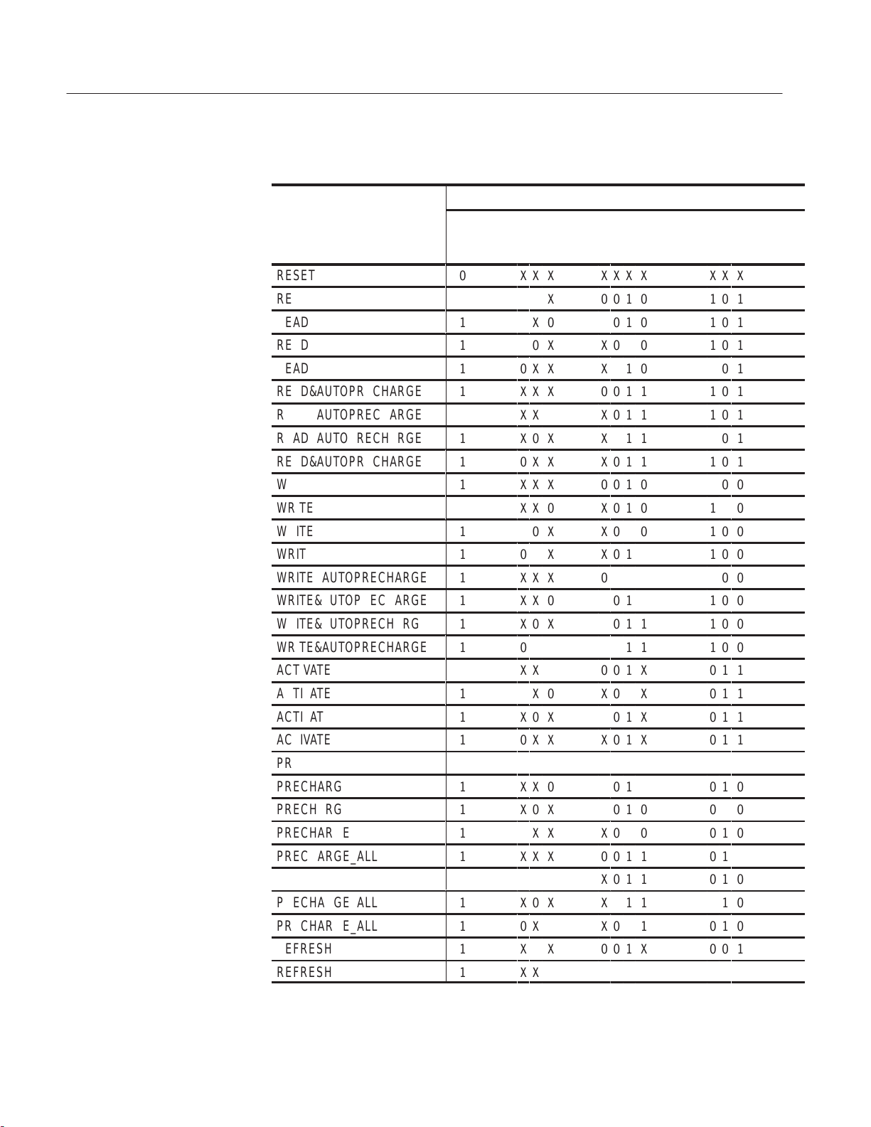
In Hardware display format, the disassembler displays certain cycle type labels in
parentheses. Table 2–2 lists cycle type labels and gives a definition of the cycle
they represent. Reads to interrupt and exception vectors are labeled with the
vector name.
T able 2–2: Cycle type definitions
Cycle type
( FLUSH )
( EXTENSION )
( ALT. BUS MASTER )
( SYSTEM RESET )
( REFRESH )
БББББББББ
( PRECHARGE )
( PRECHARGE ALL )
( ROW ADDRESS )
( COLUMN ADDRESS )
( DATA WRITE )
( DATA READ )
Definition
A cycle was fetched but not executed
An extension to the preceding instruction opcode
A bus is related to an alternate bus master
A reset cycle
A refresh cycle
БББББББББББББ
A bank precharge cycle
Precharge all bank cycle
Row address
Column address
Data write cycle
Data read cycle
( PERIPHERAL ERROR )
БББББББББ
( ALT.BUS MASTER READ )
( ALT.BUS MASTER WRITE )
( DMA READ )
( DMA WRITE )
( I-CACHE LINE FILL )
TMS532 PPC405GP Microprocessor Support
Peripheral error cycle
БББББББББББББ
Bus is related to an alternate bus master read
Bus is related to an alternate bus master write
DMA read cycle
DMA write Cycle
Instruction cache line fill
2–9
Page 27

Acquiring and Viewing Disassembled Data
Figure 2–3 shows an example of a 405GPSDRAM hardware display.
Figure 2–3: 405GPSDRAM hardware display format
Figure 2–4 shows an example of a 405GPASYNC hardware display.
2–10
Figure 2–4: 405GP ASYNC hardware display format
TMS532 PPC405GP Microprocessor Support
Page 28

Acquiring and Viewing Disassembled Data
Software Display Format
The Software display format displays only the first fetch of executed instructions.
Flushed cycles and extensions are not shown, even though they are part of the
executed instruction. Read extensions are used to disassemble the instruction, but
they are not displayed as a separate cycle in the Software display format. Data
reads and writes are not displayed. Figure 2–5 and 2–6 show examples of
software displays.
Figure 2–5: 405GPSDRAM software display format
Figure 2–6: 405GP ASYNC software display format
TMS532 PPC405GP Microprocessor Support
2–11
Page 29

Acquiring and Viewing Disassembled Data
Control Flow Display
Format
The Control Flow display format displays only the first fetch of instructions that
cause a branch in the addressing and special cycles to change the flow of control.
Figures 2–7 and 2–8 show examples of 405GPSDRAM and 405GPASYNC
control flow displays.
Figure 2–7: 405GPSDRAM control flow display format
Figure 2–8: 405GP ASYNC control flow display format
2–12
TMS532 PPC405GP Microprocessor Support
Page 30

Acquiring and Viewing Disassembled Data
Instructions that generate a change in the flow of control in the PPC405GP
microprocessor are as follows:
b target
ba target
bl target
bla target
bc BO, BI, target
bca BO, BI, target
bcl BO, BI, target
bcla BO, BI, target
bcctr BO, BI
bcctrl BO, BI
bclr BO, BI
bclrl BO, BI
Subroutine Display
Format
The Subroutine display format displays only the first fetch of subroutine call and
return instructions. It displays conditional subroutine calls if they are considered
to be taken.
Instructions that generate a subroutine call or a return in the PPC405GP
microprocessor are as follows:
rfi rfci
Changing How Data is Displayed
There are common fields and features that allow you to further modify displayed
data to suit your needs. You can make common and optional display selections in
the Disassembly property page (the Disassembly Format Definition overlay).
Optional Display
Selections
You can make optional selections for acquired disassembled data. In addition to
the common selections (described in your logic analyzer online help), you can
change the displayed data in the following ways:
Show: Hardware (default)
Software
Control Flow
Subroutine
Highlight: Software (default)
Disasm Across Gaps: Yes (default)
TMS532 PPC405GP Microprocessor Support
Control Flow
Subroutine
None
No
2–13
Page 31

Acquiring and Viewing Disassembled Data
Micro-Specific Fields
for 405GPASYNC
Endian Mode. This field allows you to indicate a PPC405GP processor configura-
tion for viewing data from memory. The following selections are available in the
order listed.
True Little Endian
Big Endian (default)
Exception Prefix. Enter an EVPR register value in this field.
0000 (default)
Byte Enable. Select either Write or Read/Write.
Read/Write (default)
Write
Bus Width. The Bus Width field is an 8 bit field and each bit represents a
chipselect (CS7, CS6, CS5, CS4, CS3, CS2, CS1, and CS0).
Enter for each chip select signal:
0 for 8 bit bus width
1 for 16 bit bus width
2 for 32 bit bus width
Micro-Specific Fields
405GPSDRAM
For example, 00000210 in a bus width field indicates that CS2 is connected to a
32 bit device, CS1 is connected to 16 bit device, and CS0 is connected to 8 bit
device.
Endian Mode. This field allows you to indicate a PPC405GP processor configuration for viewing data from memory. The following selections are available in the
order listed.
True Little Endian
Big Endian (default)
Exception Prefix. Enter an EVPR register value in this field.
0000 (default)
CAS~ Latency . Enter the CAS~ latency of the SDRAM timing register. Enter a
number between 2 and 4 (2 is the default).
2 to 4
2 (default)
2–14
TMS532 PPC405GP Microprocessor Support
Page 32

Acquiring and Viewing Disassembled Data
Á
Á
Á
Á
Á
Á
SDRAM ADDR Configuration Field. Table 2–3 lists the common configuration of
SDRAM that are fully supported by
PPC405GP EMIF. The column, SDRAM
configuration field values, lists numbers 0x0 through 0xB. Choose one of these
numbers for the appropriate SDRAM memory configuration on your board. The
default value in the SDRAM ADDR configuration field is 0x0.
NOTE. For the IBM PPC405GP
Walnut board, the PPC405GP support uses 0x7
in the SDRAM ADDR Configuration Field.
T able 2–3: Compatible SDRAM memory configuration
Bank size Organization
8 MB
БББББББ
16 MB
32 MB
64 MB
64 MB
128 MB
256 MB
8/16 MB
БББББББ
4/8 MB
16/32 MB
32 MB
11 * 9 * 2
ББББББ
11 * 10 * 2
12 * 9 * 4
12 * 10 * 4
13 * 9 * 4
13 * 11 * 4
12 * 8 * 2/4
12 * 8 * 2/4
ББББББ
11 * 9 * 2/4
13 * 8 * 2/4
13 * 9 * 2
SDRAM configuration
field values
0x0
БББББББ
0x1
0x2
0x3
0x4
0x5
0x6
0x7
БББББББ
0x8
0x9
0xA
64 MB
Bank0–4 Base Address. This field contains the bank Base address of the SDRAM
Memory configuration register for the base address field.
TMS532 PPC405GP Microprocessor Support
13 * 10 * 2
0xB
2–15
Page 33

Acquiring and Viewing Disassembled Data
Marking Cycles
TMS 532 PPC405GP support allows you to place marks using the Mark
The
Opcode button. The Mark Opcode is always available. If the sample being
marked is not an Address cycle or Data cycle of the potential bus master, the
Mark Opcode selections are replaced by a note indicating that “An Opcode Mark
cannot be placed at the selected data sample.”
When a cycle is marked, this character, >>, is displayed immediately to the left
of the Mnemonics column. Cycles can be unmarked by using the Undo Mark
selection, which removes this character. If more than one set of sequences are
marked, then the you can undo the marks by using the Remove all Marks option.
The following cycle marks are available:
H Opcode can be marked as Flush
H Flush can be marked as Opcode
Viewing an Example of Disassembled Data
A demonstration system file (or demonstration reference memory) is provided on
your PPC405GP software support disk so you can see an example of how your
PPC405GP microprocessor bus cycles and instruction mnemonics look when
they are disassembled. Viewing the system file is not a requirement for preparing
the module for use and you can view it without connecting the logic analyzer to
your system under test.
2–16
TMS532 PPC405GP Microprocessor Support
Page 34

Specifications
Page 35

Specifications
Specification Tables
This chapter contains information regarding the specifications of the
TMS 532 PPC405GP
microprocessor support.
Tables 3–1 lists the electrical requirements that the system under test must
produce for the TMS 532 PPC405GP support to acquire correct data.
T able 3–1: PPC405GP Electrical specifications
Characteristics Requirements
System under test clock rate *
405GP ASYNC Support
Maximum specified clock rate: 50 MHz
Maximum tested clock rate
Minimum setup time required: 405GPASYNC 2.5 ns
Minimum hold time required: 405GPASYNC 0 ns
405GPSDRAM Support
Maximum specified clock rate: 100 MHz
Maximum tested clock rate
Minimum setup time required 405GPSDRAM 2 ns
Minimum hold time required 405GPSDRAM 0.5 ns
* Please contact your Tektronix Sales Representative for current information on the
tested clock rate.
*
*
33 MHz
100 MHz
TMS532 PPC405GP Microprocessor Support
3–1
Page 36

Specifications
3–2
TMS532 PPC405GP Microprocessor Support
Page 37

Replaceable Parts
Page 38

Replaceable Parts
This section contains a list of the replaceable parts for the TMS 532 PPC405GP
microprocessor support product.
Parts Ordering Information
Replacement parts are available through your local Tektronix field office or
representative.
Changes to Tektronix products are sometimes made to accommodate improved
components as they become available and to give you the benefit of the latest
improvements. Therefore, when ordering parts, it is important to include the
following information in your order.
H Part number
H Instrument type or model number
H Instrument serial number
H Instrument modification number, if applicable
Abbreviations
Mfr. Code to Manufacturer
Cross Index
If you order a part that has been replaced with a different or improved part, your
local Tektronix field office or representative will contact you concerning any
change in part number.
Abbreviations conform to American National Standard ANSI Y1.1–1972.
The table titled Manufacturers Cross Index shows codes, names, and addresses
of manufacturers or vendors of components listed in the parts list.
TMS532 PPC405GP Microprocessor Support
4–1
Page 39

Replaceable Parts
Manufacturers cross index
Mfr.
code
TK2548 XEROX CORPORATION 14181 SW MILLIKAN WAY BEAVERT ON, OR 97005
80009 TEKTRONIX INC 14150 SW KARL BRAUN DR
Manufacturer Address City, state, zip code
PO BOX 500
BEAVERT ON, OR 97077–0001
Replaceable parts list
Fig. &
index
number
Tektronix
part number
071-0892-00
P6434
* 3 P6434 MASS TERMINATION PROBE, Opt 21 * 80009 ORDER BY
* Check the P6434 manual for detailed replaceable part information.
Serial no.
effective
Serial no.
discont’d
Qty Name & description Mfr. code Mfr. part number
STANDARD ACCESSORIES
1 MANUAL, TECH: INSTRUCTIONS, PPC405GP,
TMS532
OPTIONAL ACCESSORIES
TK2548
071-0892-00
DESCRIPTION
4–2
TMS532 PPC405GP Microprocessor Support
Page 40

Reference
Page 41

Reference: Tables
Á
Á
Á
Á
Á
Á
Á
Á
Á
Á
Á
Á
Á
Á
Á
Á
Á
Á
Á
Á
Á
Á
Á
Á
Á
Á
Á
Á
Á
Á
Á
Á
Á
Á
Á
Á
Á
Á
Á
Á
Á
Á
Á
Á
Á
Á
This section lists the Symbol table and the Channel group tables for disassembly
and timing.
Symbol Table
Table 5–1 lists the name, bit pattern, and meaning for the symbols in the file
405GPASYNC_Ctrl, the Control channel group symbol table.
T able 5–1: 405GPASYNC_Cntr group symbol table definitions
Symbol
ResetCycle
PeripheralError
Alt.MasterBurstRead
Alt.MasterBurstWrite
Alt.MasterSingleRead
Alt.MasterSingleWrite
Device–PacedSingleRead
Device–PacedSingleWrite
ББББББ
Device–PacedBurstRead
ББББББ
Device–PacedBurstWrite
Single/BurstReadEnd
Single/BurstWriteEnd
BurstRead
BurstWrite
DMAWrite
ББББББ
ББББББ
ББББББ
Control group value
PerErr PerR/W~ DMAAck0
PerReady PerBLast~ DMAAck1
SysReset~ ExtAck~ PerWE~ DMAAck3
0
X
1
1
1
1
1
1
ÁÁ
1
ÁÁ
1
1
1
1
1
1
ÁÁ
ÁÁ
ÁÁ
HoldAck PerOE~ DMAAck2
0XX
1XX
0X1
0X1
0X1
0X1
01X
01X
01X
01X
000
000
000
000
0XX
X
X
0
0
0
0
X
X
X
X
1
1
1
1
X
Á
Á
Á
Á
Á
XÁXXX
XÁXXX
1Á1XX
0Á1XX
1Á0XX
0Á0XX
1Á001
0
0
1
1
1
0
0Á111
1Á001
0Á010
1Á101
0Á110
0
X
X
XXX
XXX
000
000
000
000
000
0
Á
1
Á
000
000
000
000
000
000
000
X
Á
Á
Á
1
X
X
X
X
1
X
X
X
X
1
X
X
X
0
0
0
0
0
0
ÁÁ
0
ÁÁ
0
0
0
0
0
X
X
ÁÁ
X
ÁÁ
1
ÁÁ
TMS532 PPC405GP Microprocessor Support
DMARead
ББББББ
ББББББ
1
ÁÁ
ÁÁ
0XX
X
Á
Á
1
X
X
X
Á
Á
1
X
X
X
ÁÁ
X
1
X
X
X
X
1
X
ÁÁ
X
X
X
1
5–1
Page 42
Reference: Tables
Á
Á
Á
Á
Á
Á
Á
Á
Á
Á
T able 5–2: 405GPSDRAM_Cntr group symbol table definitions
Control group value
BankSelet0~
XXX
001
X01
X01
X01
001
X01
X01
X01
001
X01
X01
X01
001
X01
X01
X01
001
X01
X01
X01
001
X01
X01
X01
001
X01
X01
X01
001
X01
Symbol
RESET
READ
READ
READ
READ
READ&AUTOPRECHARGE
READ&AUTOPRECHARGE
READ&AUTOPRECHARGE
READ&AUTOPRECHARGE
WRITE
WRITE
WRITE
WRITE
WRITE&AUTOPRECHARGE
WRITE&AUTOPRECHARGE
БББББББ
WRITE&AUTOPRECHARGE
WRITE&AUTOPRECHARGE
ACTIVATE
ACTIVATE
ACTIVATE
ACTIVATE
PRECHARGE
PRECHARGE
PRECHARGE
PRECHARGE
PRECHARGE_ALL
PRECHARGE_ALL
PRECHARGE_ALL
PRECHARGE_ALL
REFRESH
REFRESH
БББББББ
BankSelet3~ HoldAck RAS~
SysReset~ BankSelet1~ D1:2 (A10)/(AP) WE~
0
1
1
1
1
1
1
1
1
1
1
1
1
1
1
ÁÁ
1
1
1
1
1
1
1
1
1
1
1
1
1
1
1
1
ÁÁ
BankSelet2~ ExtAck~ CAS~
XXX
XXX
XX0
X0X
0XX
XXX
XX0
X0X
0XX
XXX
XX0
X0X
0XX
XXX
X
X
0
ÁÁ
X0X
0XX
XXX
XX0
X0X
0XX
XXX
XX0
X0X
0XX
XXX
XX0
X0X
0XX
XXX
X
X
0
ÁÁ
X
0
0
0
0
1
1
1
1
0
0
0
0
1
1
ÁÁ
1
1
X
X
X
X
0
0
0
0
1
1
1
1
X
X
ÁÁ
XXX
101
101
101
101
101
101
101
101
100
100
100
100
100
1
0
100
100
011
011
011
011
010
010
010
010
010
010
010
010
001
0
0
0
ÁÁ
1
ÁÁ
5–2
TMS532 PPC405GP Microprocessor Support
Page 43

ÁÁÁÁ
ÁÁÁÁ
Channel Assignments
Reference: Tables
T able 5–2: 405GPSDRAM_Cntr group symbol table definitions (cont.)
Control group value
BankSelet0~
X01
X01
X
X
001
001
Symbol
REFRESH
REFRESH
BankSelet3~ HoldAck RAS~
SysReset~ BankSelet1~ D1:2 (A10)/(AP) WE~
1
1
BankSelet2~ ExtAck~ CAS~
X0X
0XX
Channel assignments listed in Tables 5–3 through 5–19 use the following
conventions:
H All signals are required by the support unless indicated otherwise.
H Channels are listed starting with the most significant bit (MSB), descending
to the least significant bit (LSB).
H Channel group assignments are for all modules unless otherwise noted.
H A tilde symbol (~) following a signal name indicates an active low signal.
H An equals symbol (=) following a signal name indicates that it is double
probed.
H The module in the lower-numbered slot is referred to as the Master module
and the module in the higher-numbered slot is referred to as the Slave
module.
The portable logic analyzer has the lower-numbered slots on the top, and the
benchtop logic analyzer has the lower-numbered slots on the left.
TMS532 PPC405GP Microprocessor Support
5–3
Page 44

Reference: Tables
405GPASYNC Support. The channel assignment groups are displayed in the
following order:
Group name Display radix
Address
Data Hexadecimal
Mnemonic None
Control Symbolic
Chip select Off
Byte Enable Off
Trace Status Off
DMAAck Off
Hexadecimal
405GPSDRAM Support. The channel assignment groups are displayed in the
following order:
Group name Display radix
BUSAddr
Data Hexadecimal
Mnemonic None
Control Symbolic
BankSelect Off
Misc Off
DataMask Off
Hexadecimal
5–4
TMS532 PPC405GP Microprocessor Support
Page 45

Reference: Tables
Á
Á
Á
Á
Table 5–3 lists the probe section and channel assignments for the Address group
and the microprocessor signal to which each channel connects. By default, the
Data channel group assignments are displayed in hexadecimal.
T able 5–3: Address channel group assignments for
405GPASYNC
Bit order Section:channel
405GPASYNC signal name
31 A3:7 PerAddr0
30 A3:6
29 A3:5
28 A3:4
27 A3:3
26 A3:2
25 A3:1
24 A3:0
23 A2:7
22 A2:6
21 A2:5
20 A2:4
19 A2:3
18 A2:2
17 A2:1
16 A2:0
15 A1:7
PerAddr1
БББББББББББ
PerAddr2
PerAddr3
PerAddr4
PerAddr5
PerAddr6
PerAddr7
PerAddr8
БББББББББББ
PerAddr9
PerAddr10
PerAddr11
PerAddr12
PerAddr13
PerAddr14
PerAddr15
БББББББББББ
PerAddr16
14 A1:6
13 A1:5
12 A1:4
11 A1:3
10 A1:2
9 A1:1
8 A1:0
7 A0:7
6 A0:6
5 A0:5
4 A0:4
TMS532 PPC405GP Microprocessor Support
PerAddr17
PerAddr18
PerAddr19
PerAddr20
PerAddr21
PerAddr22
БББББББББББ
PerAddr23
PerAddr24
PerAddr25
PerAddr26
PerAddr27
5–5
Page 46

Reference: Tables
Á
Á
T able 5–3: Address channel group assignments for
405GPASYNC (cont.)
Bit order
Section:channel
3 A0:3
2 A0:2
1 A0:1
0 A0:0
405GPASYNC signal name
PerAddr28
PerAddr29
PerAddr30
PerAddr31
БББББББББББ
Table 5–4 lists the probe section and channel assignments for the Data group and
the microprocessor signal to which each channel connects. By default, the Data
channel group assignments are displayed in hexadecimal.
T able 5–4: Data channel group assignments for 405GPASYNC
Bit order Section:channel
31 D3:7
30 D3:6
29 D3:5
28 D3:4
27 D3:3
26 D3:2
25 D3:1
24 D3:0
23 D2:7
22 D2:6
21 D2:5
20 D2:4
19 D2:3
18 D2:2
17 D2:1
16 D2:0
15 D1:7
14 D1:6
13 D1:5
12 D1:4
11 D1:3
10 D1:2
405GPASYNC signal name
PerData0
PerData1
PerData2
PerData3
PerData4
PerData5
PerData6
PerData7
PerData8
PerData9
PerData10
PerData11
PerData12
PerData13
PerData14
PerData15
PerData16
PerData17
PerData18
БББББББББББ
PerData19
PerData20
PerData21
5–6
TMS532 PPC405GP Microprocessor Support
Page 47

Reference: Tables
Á
Á
Á
Á
Á
Á
Á
T able 5–4: Data channel group assignments for 405GPASYNC
Bit order
Section:channel
9 D1:1
8 D1:0
7 D0:7
6 D0:6
5 D0:5
4 D0:4
3 D0:3
2 D0:2
1 D0:1
0 D0:0
405GPASYNC signal name
PerData22
PerData23
PerData24
PerData25
БББББББББББ
PerData26
PerData27
PerData28
PerData29
PerData30
PerData31
(cont.)
Table 5–5 lists the probe section and channel assignments for the Control group
and the microprocessor signal to which each channel connects. The default radix
of the Control group is SYMBOLIC on the logic analyzer. The symbol table file
name is 405GPASYNC_Ctrl on the logic analyzer.
T able 5–5: Control channel group assignments for 405GPASYNC
Bit order Section:channel
11
ÁÁ
10
9
8
7
6
5
4
ÁÁ
3
2
1
0
C2:1
ÁÁÁÁ
C1:3
Q1
C1:2
CLK0
CLK3
C2:0
C2:3
ÁÁÁÁ
C2:7
C2:6
C2:5
C2:4
405GPASYNC signal name
SysReset~
БББББББББББ
PerErr
PerReady
HoldAck
PerR/W~
PerBLast~
PerOE~
PerWE~
БББББББББББ
DMAAck0
DMAAck1
DMAAck2
DMAAck3
TMS532 PPC405GP Microprocessor Support
5–7
Page 48

Reference: Tables
Á
Á
Á
The Chip Select channel group assignments shown in Table 5–6 are not
displayed by default.
T able 5–6: Chip Select channel group assignments for 405GPASYNC
Bit order Section:channel
7
6
5
4
3
2
ÁÁ
1
0
C0:7
C0:6
C0:5
C0:4
C0:3
C0:2
ÁÁÁÁ
C0:1
C0:0
405GPASYNC signal name
PerCS0
PerCS1
PerCS2
PerCS3
PerCS4
PerCS5
БББББББББББ
PerCS6
PerCS7
The Byte Enable channel group assignments shown in Table 5–7 are not
displayed by default.
T able 5–7: Byte Enable channel group assignments for
405GPASYNC
Bit order Section:channel
3
C1:7
405GPASYNC signal name
PerWBE0~
5–8
2
1
0
C1:6
C1:5
C1:4
PerWBE1~
PerWBE2~
PerWBE3~
The Trace Status channel group assignments shown in Table 5–8 are not
displayed.
T able 5–8: Trace Status channel group assignments for
405GPASYNC
Bit order Section:channel 405GPASYNC signal name
7
6
5
4
C3:7
C3:6
C3:5
C3:4
TS1O
TS1E
TS2O
TS2E
TMS532 PPC405GP Microprocessor Support
Page 49

T able 5–8: Trace Status channel group assignments for
Á
Á
Á
Á
Á
405GPASYNC (cont.)
Bit order 405GP ASYNC signal nameSection:channel
Reference: Tables
3
2
1
0
C3:3
C3:2
C3:1
C3:0
TS3
TS4
TS5
TS6
The DMA Acknowledge channel group assignments shown in Table 5–9 are not
displayed by default.
T able 5–9: DMA Acknowledge channel group assignments for
405GPASYNC
Bit order Section:channel 405GPASYNC signal name
3
2
1
0
ÁÁ
C2:7
C2:6
C2:5
C2:4
ÁÁÁÁ
DMAAck0
DMAAck1
DMAAck2
DMAAck3
ББББББББББББ
Table 5–10 lists the probe section and clock and qualifier channel assignments.
The clock probes are not part of any group.
T able 5–10: Clock and Qualifier channel assignments for
405GPASYNC
Section:channel 405GPASYNC signal name
CLK:0
CLK:1
ÁÁÁÁ
CLK:3
C2:0
C2:1
C2:2
C2:3
QUAL:1
TMS532 PPC405GP Microprocessor Support
PerR/W~
PerClk
ББББББББББББББ
PerBLast~
PerOE~
SysReset~
ExtAck~
PerWE~
PerReady
5–9
Page 50

Reference: Tables
Á
Á
Á
Á
Á
Á
Acquisition Setup. The TMS 532 PPC405GP support affects the logic analyzer
setup menus (and submenus) by modifying existing fields and adding micro-specific fields.
The TMS 532 PPC405GP support adds the selection 405GPASYNC and
405GPSDRAM to the Load Support Package dialog box, under the File
pulldown menu. Once the 405GPASYNC and 405GPSDRAM supports are
loaded, the Custom clocking mode selection in the module Setup menu is also
enabled.
Table 5–11 lists the 405GPASYNC signals required for clocking and
disassembly.
T able 5–11: 405GPASYNC signals required for clocking and disassembly
Channel name PPC405GP signal name
PerAddr31–0
A3:0–7
(Address Group)
–
–
–
ББББББББ
PerData31–0
(Data Group)
–
–
CLK0
CLK1
CLK3
ББББББББ
Q1
C0:7
C0:6
C0:5
C0:4
C0:3
A2:0–7
A1:0–7
A0:0–7
–
БББББББББББББ
D3:0–7
D2:0–7
D1:0–7
D0:0–7
PerR/W~
PerClk
PerBLast~
БББББББББББББ
PerReady
PerCS0
PerCS1
PerCS2
PerCS3
PerCS4
5–10
C0:2
ББББББББ
C0:1
C0:0
C1:2
C1:3
PerCS5
БББББББББББББ
PerCS6
PerCS7
HoldAck
PerErr
TMS532 PPC405GP Microprocessor Support
Page 51

Reference: Tables
Á
Á
Á
Á
Á
Á
T able 5–11: 405GPASYNC signals required for clocking and disassembly (cont.)
Channel name PPC405GP signal name
C1:4
PerWBE3~
C1:5
C1:6
ББББББББ
C1:7
C2:0
C2:1
C2:2
C2:3
C2:4
C2:5
ББББББББ
C2:6
C2:7
PerWBE2~
PerWBE1~
БББББББББББББ
PerWBE0~
PerOE~
SysReset~
ExtAck~
PerWE~
DMAAck3
DMAAck2
БББББББББББББ
DMAAck1
DMAAck0
Table 5–12 lists the 405GPASYNC signals not required for clocking and
disassembly.
T able 5–12: 405GPASYNC signals not required for clocking and
disassembly
Channel name 405GP ASYNC signal name
C3:7
C3:6
C3:5
C3:4
C3:3
C3:2
C3:1
ББББББББ
C3:0
TMS532 PPC405GP Microprocessor Support
TS1O
TS1E
TS2O
TS2E
TS3
TS4
TS5
БББББББББ
TS6
5–11
Page 52

Reference: Tables
Á
Á
Á
Á
Á
Á
Á
Á
Á
Á
Á
Á
405GPSDRAM Channel
Group Assignments
Table 5–13 lists the probe section and channel assignments for the Address
group and the microprocessor signal to which each channel connects. By default,
the Address channel group assignments are displayed in hexadecimal.
T able 5–13: TLA Group A channel assignments for 405GPSDRAM
Bit order Channel name 405GPSDRAM signal name
0
1
2
3
4
5
ÁÁ
6
7
8
9
10
A3:7
A3:6
A3:5
A3:4
A3:3
A3:2
ÁÁÁÁ
A3:1
A3:0
A2:7
A2:6
A2:5
MemData0
MemData1
MemData2
MemData3
MemData4
MemData5
ББББББББББББ
MemData6
MemData7
MemData8
MemData9
MemData10
11
12
ÁÁ
13
14
15
16
17
18
19
ÁÁ
20
21
22
23
24
25
26
ÁÁ
27
A2:4
A2:3
ÁÁÁÁ
A2:2
A2:1
A2:0
A1:7
A1:6
A1:5
A1:4
ÁÁÁÁ
A1:3
A1:2
A1:1
A1:0
A0:7
A0:6
A0:5
ÁÁÁÁ
A0:4
MemData11
MemData12
ББББББББББББ
MemData13
MemData14
MemData15
MemData16
MemData17
MemData18
MemData19
ББББББББББББ
MemData20
MemData21
MemData22
MemData23
MemData24
MemData25
MemData26
ББББББББББББ
MemData27
5–12
28
A0:3
MemData28
TMS532 PPC405GP Microprocessor Support
Page 53

Reference: Tables
Á
Á
Á
Á
Á
Á
T able 5–13: TLA Group A channel assignments for 405GPSDRAM (cont.)
Bit order 405GPSDRAM signal nameChannel name
29
A0:2
MemData29
30
31
ÁÁ
A0:1
A0:0
ÁÁÁÁ
MemData30
MemData31
ББББББББББББ
Table 5–14 lists the probe section and channel assignments for the Data group
and the microprocessor signal to which each channel connects. By default, the
Data channel group assignments are displayed in hexadecimal.
T able 5–14: TLA group D channel assignments for 405GPSDRAM
405GPSDRAM
Bit order Channel name
12
11
10
9
8
7
6
ÁÁ
5
D0:0
D0:1
D0:2
D0:3
D0:4
D0:5
D0:6
ÁÁÁÁ
D0:7
signal name
MemAddr0
MemAddr1
MemAddr2
MemAddr3
MemAddr4
MemAddr5
MemAddr6
ББББББББББББ
MemAddr7
4
3
2
1
0
TMS532 PPC405GP Microprocessor Support
D1:0
D1:1
D1:2
D1:3
D1:4
MemAddr8
MemAddr9
MemAddr10
MemAddr11
MemAddr12
5–13
Page 54

Reference: Tables
Á
Á
Á
Á
Á
Á
Á
Table 5–15 lists the probe section and clock and qualifier channel assignments.
The clock probes are not part of any group.
T able 5–15: Clock and Qualifier channel assignments for
405GPSDRAM
Channel
name
CLK:3
ÁÁ
C2:0
C2:1
C2:2
405GPSDRAM
signal name
MemClkOut0
ÁÁÁ
RAS~
CAS~
WE~
Comments
–
ББББББ
RowAddressStrobe
ColoumAddressStrobe
WriteEnable
CLK
ÁÁÁÁ
Qual
Qual
Qual
Table 5–16 lists the Bank Select channel assignments. By default, this channel
group is not displayed.
T able 5–16: Bank Select channel assignments for
405GPSDRAM
Bit
order
3
2
ÁÁ
1
Channel
name
C3:0
C3:1
ÁÁ
C3:2
405GPSDRAM
signal name
BankSel3~
BankSel2~
ББББББББББББ
BankSel1~
5–14
0
C3:3
BankSel0~
Table 5–17 lists the Bank Access channel assignments. By default, this channel
group is not displayed.
T able 5–17: Bank Access channel assignments for
405GPSDRAM
Bit
order
1
0
Channel
name
D1:6
D1:7
405GPSDRAM
signal name
BA0
BA1
TMS532 PPC405GP Microprocessor Support
Page 55
Reference: Tables
Á
Á
Á
Á
Á
Á
Á
Á
Á
Table 5–18 lists the Data Mask channel assignments. By default, this channel
group is not displayed.
T able 5–18: Data Mask channel assignments for
405GPSDRAM
Bit
order
3
ÁÁ
2
1
0
Channel
name
C2:4
Á
C2:5
C2:6
C2:7
405GPSDRAM
signal name
DQM3
БББББББББББББ
DQM2
DQM1
DQM0
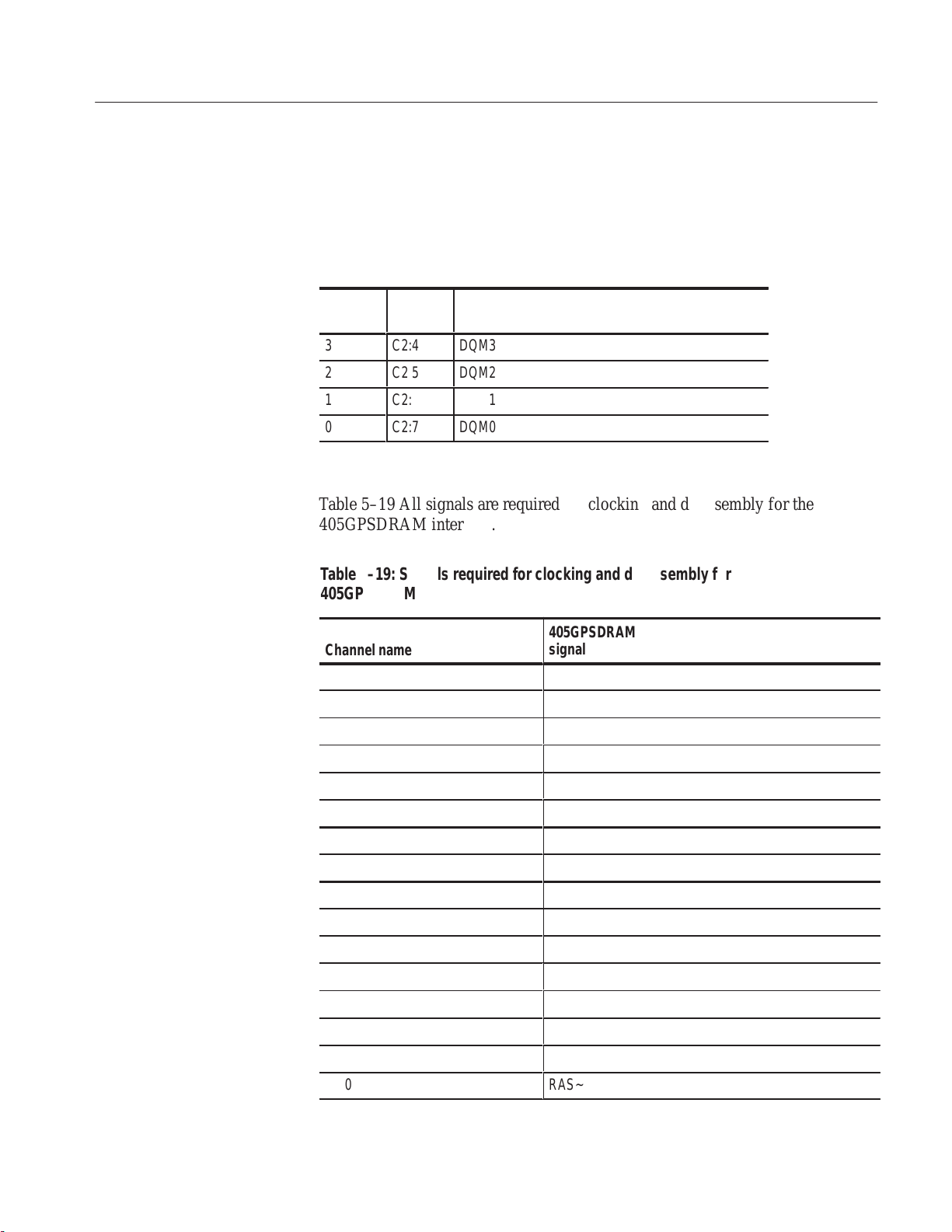
Table 5–19 All signals are required for clocking and disassembly for the
405GPSDRAM interface.
T able 5–19: Signals required for clocking and disassembly for
405GPSDRAM
405GPSDRAM
Channel name
MemAddr12–0
(Address Group)
ББББББББ
MemData31:0
signal name
D0:7–0
D1:4–0
БББББББББББББ
A3:0–7
(Data Group)
–
–
CLK:0
CLK:2
CLK:3
ББББББББ
C3:0
C3:1
C3:2
C3:3
C2:2
C2:1
C2:0
ББББББББ
TMS532 PPC405GP Microprocessor Support
A2:0–7
A1:0–7
A0:0–7
SysReset~
ExtAck~
MemClkOut0
БББББББББББББ
BankSel3~
BankSel2~
BankSel1~
BankSel0~
WE~
CAS~
RAS~
БББББББББББББ
5–15
Page 56

Reference: Tables
Á
Á
T able 5–19: Signals required for clocking and disassembly for
405GPSDRAM (cont.)
405GPSDRAM
Channel name
D1:6
signal name
BA0
D1:7
C2:7
C2:6
C2:5
C2:4
ББББББББ
C2:3
BA1
DQM0
DQM1
DQM2
DQM3
БББББББББББББ
HoldAck
5–16
TMS532 PPC405GP Microprocessor Support
Page 57

CPU To Mictor Connections
To probe the microprocessor you need to make connections between the CPU
and the Mictor pins of the P6434 Mass Termination Probe. Refer to the P6434
Mass Termination Probe manual, Tektronix part number 070-9793-xx, for more
information on mechanical specifications. Tables 5–20 through 5–24 list the
CPU pin to Mictor pin connections.
Tektronix uses a counterclockwise pin assignment. Pin 1 is located at the top left,
and pin 2 is located directly below it. Pin 20 is located on the bottom right, and
pin 21 is located directly above it.
AMP uses an odd side even side pin assignment. Pin 1 is located at the top left,
and pin 3 is located directly below it. Pin 2 is located on the top right, and pin 4
is located directly below it (see Figure 5–1).
NOTE. When designing Mictor connectors into your system under test, always
follow the Tektronix pin assignment.
Reference: Tables
Tektronix Pinout AMP Pinout
Pin 1
Pin 19
Pin 38
Pin 20
Pin 1
Pin 37
Pin 2
Pin 38
Figure 5–1: Pin assignments for a Mictor connector (component side)
CAUTION. To protect the CPU and the inputs of the module, it is recommended
that a 180 W resistor is connected in series between each ball pad of the CPU
and each pin of the Mictor connector. The resistor must be within 1/2 inch of the
ball pad of the CPU.
TMS532 PPC405GP Microprocessor Support
5–17
Page 58

Reference: Tables
Á
Á
Á
Á
Á
Á
Á
Á
Á
Á
Á
Á
Á
Á
Á
Á
Á
Á
Á
Á
405GPASYNC Mictor
Connections
Tables 5–20 through 5–22 list the microprocessor signals visible at the mictor
connectors.
T able 5–20: CPU to Mictor connections for Mictor A pins for 405GPASYNC
Tektronix
Mictor A
pin number
01
02
ÁÁÁÁ
03
04
05
06
07
08
09
ÁÁÁÁ
10
11
AMP
Mictor A
pin number
01
03
ÁÁÁ
05
07
09
11
13
15
17
ÁÁÁ
19
21
Logic
analyzer
channel
–
–
ÁÁÁ
Clock 0
A3:7
A3:6
A3:5
A3:4
A3:3
A3:2
ÁÁÁ
A3:1
A3:0
405GPASYNC
signal name
–
–
ÁÁÁÁ
PerR/W~
Addr 0
Addr 1
Addr 2
Addr 3
Addr 4
Addr 5
ÁÁÁÁ
Addr 6
Addr 7
Comments
Not Connected
Not Connected
ÁÁÁÁ
Read/Write
ASYNC Address
ASYNC Address
ASYNC Address
ASYNC Address
ASYNC Address
ASYNC Address
ÁÁÁÁ
ASYNC Address
ASYNC Address
12
13
14
15
16
ÁÁÁÁ
17
18
19
20
21
22
23
ÁÁÁÁ
24
25
26
27
28
23
25
27
29
31
ÁÁÁ
33
35
37
38
36
34
32
ÁÁÁ
30
28
26
24
22
A2:7
A2:6
A2:5
A2:4
A2:3
ÁÁÁ
A2:2
A2:1
A2:0
A0:0
A0:1
A0:2
A0:3
ÁÁÁ
A0:4
A0:5
A0:6
A0:7
A1:0
Addr 8
Addr 9
Addr 10
Addr 11
Addr 12
ÁÁÁÁ
Addr 13
Addr 14
Addr 15
Addr 31
Addr 30
Addr 29
Addr 28
ÁÁÁÁ
Addr 27
Addr 26
Addr 25
Addr 24
Addr 23
ASYNC Address
ASYNC Address
ASYNC Address
ASYNC Address
ASYNC Address
ÁÁÁÁ
ASYNC Address
ASYNC Address
ASYNC Address
ASYNC Address
ASYNC Address
ASYNC Address
ASYNC Address
ÁÁÁÁ
ASYNC Address
ASYNC Address
ASYNC Address
ASYNC Address
ASYNC Address
5–18
TMS532 PPC405GP Microprocessor Support
Page 59
Reference: Tables
Á
Á
Á
Á
Á
Á
Á
Á
Á
Á
Á
Á
Á
Á
Á
Á
Á
Á
Á
Á
T able 5–20: CPU to Mictor connections for Mictor A pins for 405GPASYNC (cont.)
Tektronix
Mictor A
pin number
29
30
31
32
33
34
35
ÁÁÁÁ
36
AMP
Mictor A
pin number
20
18
16
14
12
10
08
ÁÁÁ
06
Logic
analyzer
channel
A1:1
A1:2
A1:3
A1:4
A1:5
A1:6
A1:7
ÁÁÁ
Clock 1
405GPASYNC
signal name
Addr 22
Addr 21
Addr 20
Addr 19
Addr 18
Addr 17
Addr 16
ÁÁÁÁ
PerClk
Comments
ASYNC Address
ASYNC Address
ASYNC Address
ASYNC Address
ASYNC Address
ASYNC Address
ASYNC Address
ÁÁÁÁ
ASYNC Clock
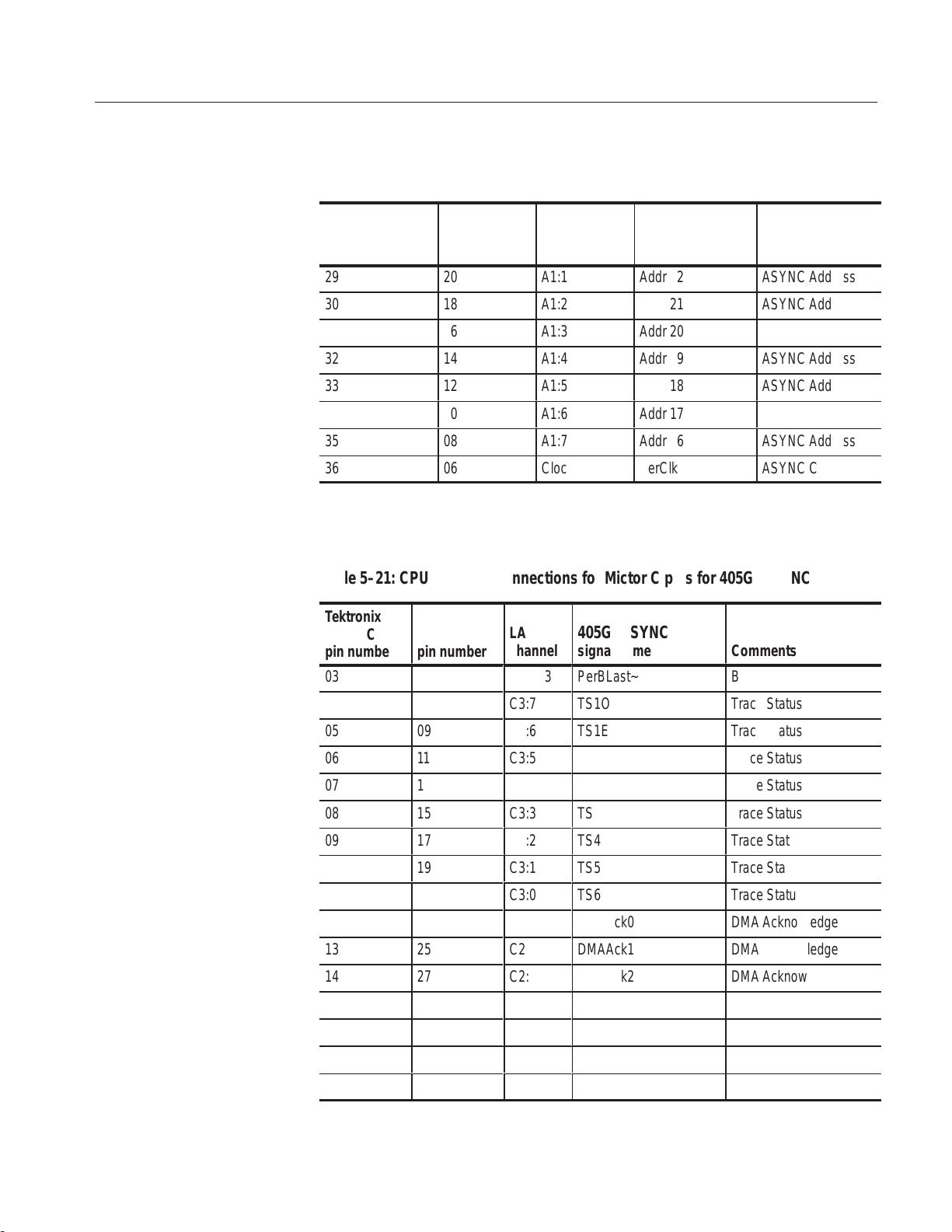
T able 5–21: CPU to Mictor connections for Mictor C pins for 405GPASYNC
Tektronix
Mictor C
pin number
03
AMP
Mictor C
pin number
05
LA
channel
Clock 3
405GPASYNC
signal name
PerBLast~
Comments
Burst Last
04
ÁÁÁ
05
06
07
08
09
10
11
ÁÁÁ
12
13
14
15
16
17
18
ÁÁÁ
07
ÁÁÁ
09
11
13
15
17
19
21
ÁÁÁ
23
25
27
29
31
33
35
ÁÁÁ
C3:7
C3:6
C3:5
C3:4
C3:3
C3:2
C3:1
C3:0
C2:7
C2:6
C2:5
C2:4
C2:3
C2:2
C2:1
Á
Á
Á
TS1O
ББББББ
TS1E
TS2O
TS2E
TS3
TS4
TS5
TS6
ББББББ
DMAAck0
DMAAck1
DMAAck2
DMAAck3
PerWE~
ExtAck~
SysReset~
ББББББ
Trace Status
БББББ
Trace Status
Trace Status
Trace Status
Trace Status
Trace Status
Trace Status
Trace Status
БББББ
DMA Acknowledge
DMA Acknowledge
DMA Acknowledge
DMA Acknowledge
ASYNC Write Enable
External Acknowledge
System Reset
БББББ
TMS532 PPC405GP Microprocessor Support
5–19
Page 60

Reference: Tables
БББББББ
БББББББ
БББББББ
БББББББ
БББББББ
БББББББ
Á
Á
Á
БББББББ
Á
Á
Á
БББББББ
БББББББ
БББББББ
БББББББ
БББББББ
БББББББ
Á
Á
Á
БББББББ
Á
Á
Á
Á
Á
Á
БББББББ
Á
Á
Á
Á
Á
Á
БББББББ
Á
Á
Á
Á
Á
Á
БББББББ
Á
Á
Á
БББББББ
БББББББ
БББББББ
БББББББ
БББББББ
БББББББ
T able 5–21: CPU to Mictor connections for Mictor C pins for 405GPASYNC (cont.)
Tektronix
Mictor C
pin number
19
20
21
22
23
24
25
ÁÁÁ
26
27
28
29
30
31
32
ÁÁÁ
AMP
Mictor C
pin number
37
38
36
34
32
30
28
ÁÁÁ
26
24
22
20
18
16
14
ÁÁÁ
LA
channel
C2:0
C0:0
C0:1
C0:2
C0:3
C0:4
C0:5
ÁÁ
C0:6
C0:7
C1:0
C1:1
C1:2
C1:3
C1:4
ÁÁ
405GPASYNC
signal name
PerOE~
PerCS7
PerCS6
PerCS5
PerCS4
PerCS3
PerCS2
БББББ
PerCS1
PerCS0
–
–
HoldAck
PerErr
PerWBE3~
БББББ
Comments
ASYNC Output Enable
Chip Select
Chip Select
Chip Select
Chip Select
Chip Select
Chip Select
БББББ
Chip Select
Chip Select
–
–
Hold Acknowledge
ASYNC Error
ASYNC WriteByteEn-
БББББ
able
33
ÁÁÁ
34
ÁÁÁ
35
ÁÁÁ
36
37
38
12
ÁÁÁ
10
ÁÁÁ
08
ÁÁÁ
06
04
02
C1:5
ÁÁ
C1:6
ÁÁ
C1:7
ÁÁ
Qual 1
–
–
PerWBE2~
БББББ
PerWBE1~
БББББ
PerWBE0~
БББББ
PerReady
–
–
ASYNC WriteByteEn-
БББББ
able
ASYNC WriteByteEn-
БББББ
able
ASYNC WriteByteEn-
БББББ
able
ASYNC Ready
Not Connected
Not Connected
T able 5–22: CPU to Mictor connections for Mictor D pins for 405GPASYNC
Tektronix
Mictor D
pin number
01
02
03
AMP
Mictor D
pin number
01
03
05
LA
channel
–
–
–
405GPASYNC
signal name
–
–
–
Comments
Not Connected
Not Connected
Not Connected
5–20
TMS532 PPC405GP Microprocessor Support
Page 61

Reference: Tables
Á
Á
Á
Á
Á
Á
Á
Á
Á
Á
Á
Á
Á
Á
Á
Á
Á
Á
Á
Á
T able 5–22: CPU to Mictor connections for Mictor D pins for 405GPASYNC (cont.)
Tektronix
Mictor D
pin number
04
05
06
07
08
09
10
ÁÁÁ
11
12
13
14
15
16
17
ÁÁÁ
18
AMP
Mictor D
pin number
07
09
11
13
15
17
19
ÁÁÁ
21
23
25
27
29
31
33
ÁÁÁ
35
LA
channel
D3:7
D3:6
D3:5
D3:4
D3:3
D3:2
D3:1
Á
D3:0
D2:7
D2:6
D2:5
D2:4
D2:3
D2:2
Á
D2:1
405GPASYNC
signal name
PerData 0
PerData 1
PerData 2
PerData 3
PerData 4
PerData 5
PerData 6
ББББББ
PerData 7
PerData 8
PerData 9
PerData 10
PerData 11
PerData 12
PerData 13
ББББББ
PerData 14
Comments
Peripheral Data
Peripheral Data
Peripheral Data
Peripheral Data
Peripheral Data
Peripheral Data
Peripheral Data
БББББ
Peripheral Data
Peripheral Data
Peripheral Data
Peripheral Data
Peripheral Data
Peripheral Data
Peripheral Data
БББББ
Peripheral Data
19
20
21
22
23
24
ÁÁÁ
25
26
27
28
29
30
31
ÁÁÁ
32
33
34
37
38
36
34
32
30
ÁÁÁ
28
26
24
22
20
18
16
ÁÁÁ
14
12
10
D2:0
D0:0
D0:1
D0:2
D0:3
D0:4
D0:5
D0:6
D0:7
D1:0
D1:1
D1:2
D1:3
D1:4
D1:5
D1:6
Á
Á
PerData 15
PerData 31
PerData 30
PerData 29
PerData 28
PerData 27
ББББББ
PerData 26
PerData 25
PerData 24
PerData 23
PerData 22
PerData 21
PerData 20
ББББББ
PerData 19
PerData 18
PerData 17
Peripheral Data
Peripheral Data
Peripheral Data
Peripheral Data
Peripheral Data
Peripheral Data
БББББ
Peripheral Data
Peripheral Data
Peripheral Data
Peripheral Data
Peripheral Data
Peripheral Data
Peripheral Data
БББББ
Peripheral Data
Peripheral Data
Peripheral Data
TMS532 PPC405GP Microprocessor Support
5–21
Page 62

Reference: Tables
БББББББ
БББББББ
Á
Á
Á
БББББББ
Á
Á
Á
БББББББ
БББББББ
БББББББ
БББББББ
БББББББ
БББББББ
Á
Á
Á
БББББББ
Á
Á
Á
БББББББ
БББББББ
БББББББ
БББББББ
БББББББ
БББББББ
Á
Á
Á
БББББББ
Á
Á
Á
БББББББ
БББББББ
БББББББ
БББББББ
БББББББ
БББББББ
T able 5–22: CPU to Mictor connections for Mictor D pins for 405GPASYNC (cont.)
405GPSDRAM Mictor
Connections
Tektronix
Mictor D
pin number
35
36
AMP
Mictor D
pin number
08
06
LA
channel
D1:7
–
405GPASYNC
signal name
PerData 16
–
Comments
Peripheral Data
Not Connected
Tables 5–23 and 5–24 list the microprocessor signals visible at the mictor
connectors.
T able 5–23: CPU to Mictor connections for Mictor A pins for 405GPSDRAM
Tektronix
Mictor A
pin number
01
ÁÁÁ
02
03
04
05
AMP
Mictor A
pin number
01
ÁÁÁ
03
05
07
09
LA
channel
–
ÁÁ
–
Clock:0
A3:7
A3:6
405GPSDRAM
signal name
–
БББББ
–
SysReset~
MemData0
MemData1
Comments
Not Connected
БББББ
Not Connected
SystemReset
SDRAM Data
SDRAM Data
06
07
08
ÁÁÁ
09
10
11
12
13
14
15
ÁÁÁ
16
17
18
19
20
21
11
13
15
ÁÁÁ
17
19
21
23
25
27
29
ÁÁÁ
31
33
35
37
38
A36
A3:5
A3:4
A3:3
ÁÁ
A3:2
A3:1
A3:0
A2:7
A2:6
A2:5
A2:4
ÁÁ
A2:3
A2:2
A2:1
A2:0
A0:0
A0:1
MemData2
MemData3
MemData4
БББББ
MemData5
MemData6
MemData7
MemData8
MemData9
MemData10
MemData11
БББББ
MemData12
MemData13
MemData14
MemData15
MemData31
MemData30
SDRAM Data
SDRAM Data
SDRAM Data
БББББ
SDRAM Data
SDRAM Data
SDRAM Data
SDRAM Data
SDRAM Data
SDRAM Data
SDRAM Data
БББББ
SDRAM Data
SDRAM Data
SDRAM Data
SDRAM Data
SDRAM Data
SDRAM Data
5–22
TMS532 PPC405GP Microprocessor Support
Page 63
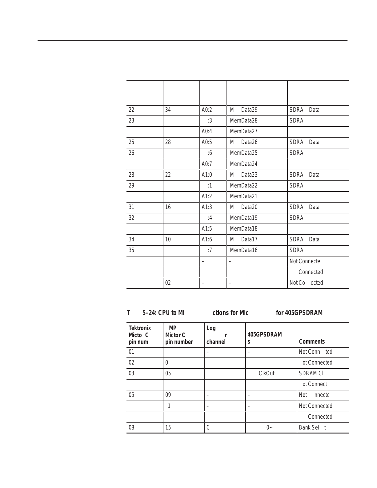
Reference: Tables
Á
Á
Á
Á
Á
Á
Á
Á
Á
Á
Á
Á
Á
Á
Á
T able 5–23: CPU to Mictor connections for Mictor A pins for 405GPSDRAM (cont.)
Tektronix
Mictor A
pin number
22
23
24
25
26
27
28
ÁÁÁ
29
30
31
32
33
34
35
ÁÁÁ
36
AMP
Mictor A
pin number
34
32
30
28
26
24
22
ÁÁÁ
20
18
16
14
12
10
08
ÁÁÁ
06
LA
channel
A0:2
A0:3
A0:4
A0:5
A0:6
A0:7
A1:0
Á
A1:1
A1:2
A1:3
A1:4
A1:5
A1:6
A1:7
Á
–
405GPSDRAM
signal name
MemData29
MemData28
MemData27
MemData26
MemData25
MemData24
MemData23
ББББББ
MemData22
MemData21
MemData20
MemData19
MemData18
MemData17
MemData16
ББББББ
–
Comments
SDRAM Data
SDRAM Data
SDRAM Data
SDRAM Data
SDRAM Data
SDRAM Data
SDRAM Data
БББББ
SDRAM Data
SDRAM Data
SDRAM Data
SDRAM Data
SDRAM Data
SDRAM Data
SDRAM Data
БББББ
Not Connected
37
38
04
02
–
–
–
–
Not Connected
Not Connected
T able 5–24: CPU to Mictor connections for Mictor C pins for 405GPSDRAM
Tektronix
Mictor C
pin number
01
02
03
ÁÁÁ
04
05
06
07
08
AMP
Mictor C
pin number
01
03
05
ÁÁÁ
07
09
11
13
15
Logic
analyzer
channel
–
–
Clock:3
ÁÁÁ
–
–
–
–
C3:3
405GPSDRAM
signal name
–
–
MemClkOut
БББББ
–
–
–
–
BankSel0~
Comments
Not Connected
Not Connected
SDRAM Clock
ÁÁÁÁ
Not Connected
Not Connected
Not Connected
Not Connected
Bank Select
TMS532 PPC405GP Microprocessor Support
5–23
Page 64

Reference: Tables
ББББББ
ББББББ
ББББББ
ББББББ
ББББББ
ББББББ
Á
Á
Á
ББББББ
Á
Á
ББББББ
ББББББ
Á
Á
Á
ББББББ
Á
Á
ББББББ
ББББББ
ББББББ
ББББББ
ББББББ
Á
Á
Á
ББББББ
Á
Á
ББББББ
ББББББ
ББББББ
ББББББ
ББББББ
ББББББ
Á
Á
Á
ББББББ
Á
Á
ББББББ
ББББББ
ББББББ
ББББББ
Á
Á
Á
ББББББ
Á
Á
ББББББ
ББББББ
T able 5–24: CPU to Mictor connections for Mictor C pins for 405GPSDRAM (cont.)
Tektronix
Mictor C
pin number
09
10
11
12
13
14
15
ÁÁÁ
16
17
18
ÁÁÁ
19
20
21
22
AMP
Mictor C
pin number
17
19
21
23
25
27
29
ÁÁÁ
31
33
35
ÁÁÁ
37
38
36
34
Logic
analyzer
channel
C3:2
C3:1
C3:0
C2:7
C2:6
C2:5
C2:4
ÁÁÁ
C2:3
C2:2
C2:1
ÁÁÁ
C2:0
D0:0
D0:1
D0:2
405GPSDRAM
signal name
BankSel1~
BankSel2~
BankSel3~
DQM0
DQM1
DQM2
DQM3
БББББ
HoldAck
WE~
CAS~
БББББ
RAS~
MemAddr0
MemAddr1
MemAddr2
Comments
Bank Select
Bank Select
Bank Select
Data Mask
Data Mask
Data Mask
Data Mask
ÁÁÁÁ
HoldAck
WriteEnable
ColumnAddress-
Strobe
ÁÁÁÁ
RowAddressStrobe
SDRAM Address
SDRAM Address
SDRAM Address
23
24
ÁÁÁ
25
26
27
28
29
30
31
ÁÁÁ
32
33
34
35
36
ÁÁÁ
37
38
32
30
ÁÁÁ
28
26
24
22
20
18
16
ÁÁÁ
14
12
10
08
06
ÁÁÁ
04
02
D0:3
D0:4
ÁÁÁ
D0:5
D0:6
D0:7
D1:0
D1:1
D1:2
D1:3
ÁÁÁ
D1:4
D1:5
D1:6
D1:7
Clock:2
ÁÁÁ
–
–
MemAddr3
MemAddr4
БББББ
MemAddr5
MemAddr6
MemAddr7
MemAddr8
MemAddr9
MemAddr10
MemAddr11
БББББ
MemAddr12
MemAddr13
BA0
BA1
ExtAck~
БББББ
–
–
SDRAM Address
SDRAM Address
ÁÁÁÁ
SDRAM Address
SDRAM Address
SDRAM Address
SDRAM Address
SDRAM Address
SDRAM Address
SDRAM Address
ÁÁÁÁ
SDRAM Address
SDRAM Address
BankAddress
BankAddress
External
ÁÁÁÁ
Acknowledge
Not Connected
Not Connected
5–24
TMS532 PPC405GP Microprocessor Support
Page 65

Index
Page 66

Page 67

Index
Numbers
405GPASYNC channel assignments
Address group, 5–5
BEnable group, 5–8
ChipSelect group, 5–8
clocks and qualifiers, 5–9
control group, 5–7
data group, 5–6
DMA Acknowledge group, 5–9
Trace Status group, 5–8
405GPSDRAM channel assignments, 5–14
address group, 5–12
bank access group, 5–14
bank select group, 5–14
clocks and qualifiers, 5–14
data group, 5–13
data mask group, 5–15
A
About this manual set, ix
Address, T ektronix, x
Address group
405GPASYNC channel assignments, 5–5
405GPSDRAM channel assignments, 5–12
Application, logic analyzer configuration, 1–1
ASYNC C6201 clock rate, SUT, 3–1
ASYNC Electrical specifications, C6201 clock rate, 3–1
ASYNC Hold time, minimum, 3–1
ASYNC Set up time, minimum, 3–1
B
Bank Access group, 405GPSDRAM channel assign-
ments, 5–14
Bank Select group, 405GPSDRAM channel assign-
ments, 5–14
BEnable group, 405GPASYNC channel assignments,
5–8
Bus cycles, displayed cycle types, 2–9
C
C6201 loading, PPC405GP, 3–1
Channel groups, 2–2
visibility , 2–7
ChipSelect group, 405GPASYNC channel assignments,
5–8
Clock rate, 1–2
Clocking, custom, 2–4
Clocking Options
external clocking, 2–4
internal clocking, 2–4
Clocking options, 2–4
Connections
CPU to Mictor, 5–17
no probe adapter, 1–4
Contacting T ektronix, x
Control flow display format, 2–12
Control group
405GPASYNC channel assignments, 5–7
symbol tables, 5–1
CPU to Mictor connections, 5–17
Custom clocking, 2–4
Cycle types, 2–9
D
Data
disassembly formats, Timing-Display, 2–8
disassembly formats
control Flow, 2-12
hardware, 2-9
software, 2-11
subroutine, 2-13
Data display , changing, 2–13
Data group
405GPASYNC channel assignments, 5–6
405GPSDRAM channel assignments, 5–13
Data Mask group, 405GPSDRAM channel assignments,
5–15
Definitions
disassembler, ix
information on basic operations, ix
Demonstration file, 2–16
Disassembled data
cycle type definitions, 2–9
viewing, 2–7
viewing an example, 2–16
Disassembler
definition, ix
TMS532 PPC405GP Microprocessor Support
Index–1
Page 68

Index
logic analyzer configuration, 1–1
setup, 2–1
Disassembly format definition overlay, 2–13
Disassembly property page, 2–13
Display formats
control Flow, 2–12
hardware, 2–9
software, 2–11
special characters, 2–7
subroutine, 2–13
timing-Display, 2–8
DMA Acknowledge group, 405GPASYNC channel
assignments, 5–9
DRAM C6201 clock rate, SUT , 3 –1
DRAM Electrical specifications, C6201 clock rate, 3–1
DRAM Hold time, minimum, 3–1
DRAM Set up time, minimum, 3–1
E
Electrical specifications, 3–1
PPC405GP, 3–1
H
Hardware display format, 2–9
cycle type definitions, 2–9
I
Installing support software, 2–1
L
Logic analyzer
configuration for disassembler, 1–1
configuration for the application, 1–1
software compatibility, 1–1
M
Manual
conventions, ix
how to use the set, ix
Mark Cycle function, 2–16
Mark Opcode function, 2–16
Marking cycles, definition of, 2–16
Micro Specific Fields, SDRAM addr configuration,
2–15
Mictor to CPU connections, 5–17
O
Options, 1–3
P
Phone number, Tektronix, x
Probe adapter, not using one, 1–4
Product support, contact information, x
R
Reference, channel assignments, 5–3
Reference memory, 2–16
Restrictions, 1–2
without a probe adapter, 1–4
S
SDRAM addr configuration, 2–15
Service support, contact information, x
Setups
disassembler, 2–1
support, 2–1
Signals not required for disassembly, 405GPASYNC
support, 5–11
Signals required for disssembly
405GPASYNC support, 5–10
405GPSDRAM support, 5–15
Software display format, 2–11
Special characters displayed, 2–7
Specifications, 3–1
electrical, 3–1
Standard accessories, 1–3
Subroutine display format, 2–13
Support, setup, 2–1
Support package setups
disassembly, 2–3
timing, 2–3
Support setup, 2–1
Symbol tables, control channel group, 5–1
System file, demonstration, 2–16
T
T echnical support, contact information, x
T ektronix, contacting, x
T erminology, ix
Timing-display format, 2–8
Trace Status group, 405GPASYNC channel assignments,
5–8
Index–2
TMS532 PPC405GP Microprocessor Support
Page 69

Index
U
URL, Tektronix, x
V
Viewing disassembled data, 2–7
W
Web site address, T ektronix, x
TMS532 PPC405GP Microprocessor Support
Index–3
Page 70

Index
Index–4
TMS532 PPC405GP Microprocessor Support
 Loading...