

Page 1

Instruction Manual
TMS 260
CPU32 Family Microprocessor Support
070-9824-00
There are no current European directives that
apply to this product. This product provides
cable and test lead connections to a test object of
electronic measuring and test equipment.
Warning
The servicing instructions are for use by
qualified personnel only. To avoid personal
injury, do not perform any servicing unless you
are qualified to do so. Refer to all safety
summaries prior to performing service.
Page 2

Copyright T ektronix, Inc. All rights reserved. Licensed software products are owned by Tektronix or its suppliers and are
protected by United States copyright laws and international treaty provisions.
Use, duplication, or disclosure by the Government is subject to restrictions as set forth in subparagraph (c)(1)(ii) of the
Rights in T echnical Data and Computer Software clause at DFARS 252.227-7013, or subparagraphs (c)(1) and (2) of the
Commercial Computer Software – Restricted Rights clause at F AR 52.227-19, as applicable.
T ektronix products are covered by U.S. and foreign patents, issued and pending. Information in this publication supercedes
that in all previously published material. Specifications and price change privileges reserved.
Printed in the U.S.A.
T ektronix, Inc., P.O. Box 1000, Wilsonville, OR 97070–1000
TEKTRONIX and TEK are registered trademarks of T ektronix, Inc.
Page 3

SOFTWARE WARRANTY
T ektronix warrants that the media on which this software product is furnished and the encoding of the programs on
the media will be free from defects in materials and workmanship for a period of three (3) months from the date of
shipment. If a medium or encoding proves defective during the warranty period, T ektronix will provide a
replacement in exchange for the defective medium. Except as to the media on which this software product is
furnished, this software product is provided “as is” without warranty of any kind, either express or implied.
T ektronix does not warrant that the functions contained in this software product will meet Customer’s
requirements or that the operation of the programs will be uninterrupted or error-free.
In order to obtain service under this warranty, Customer must notify Tektronix of the defect before the expiration
of the warranty period. If T ektronix is unable to provide a replacement that is free from defects in materials and
workmanship within a reasonable time thereafter, Customer may terminate the license for this software product
and return this software product and any associated materials for credit or refund.
THIS WARRANTY IS GIVEN BY TEKTRONIX IN LIEU OF ANY OTHER WARRANTIES, EXPRESS
OR IMPLIED. TEKTRONIX AND ITS VENDORS DISCLAIM ANY IMPLIED WARRANTIES OF
MERCHANTABILITY OR FITNESS FOR A PARTICULAR PURPOSE. TEKTRONIX’
RESPONSIBILITY TO REPLACE DEFECTIVE MEDIA OR REFUND CUSTOMER’S PAYMENT IS
THE SOLE AND EXCLUSIVE REMEDY PROVIDED TO THE CUSTOMER FOR BREACH OF THIS
WARRANTY. TEKTRONIX AND ITS VENDORS WILL NOT BE LIABLE FOR ANY INDIRECT,
SPECIAL, INCIDENTAL, OR CONSEQUENTIAL DAMAGES IRRESPECTIVE OF WHETHER
TEKTRONIX OR THE VENDOR HAS ADVANCE NOTICE OF THE POSSIBILITY OF SUCH
DAMAGES.
Page 4

HARDWARE WARRANTY
T ektronix warrants that the products that it manufactures and sells will be free from defects in materials and
workmanship for a period of one (1) year from the date of shipment. If a product proves defective during this
warranty period, T ektronix, at its option, either will repair the defective product without charge for parts and labor,
or will provide a replacement in exchange for the defective product.
In order to obtain service under this warranty, Customer must notify Tektronix of the defect before the expiration
of the warranty period and make suitable arrangements for the performance of service. Customer shall be
responsible for packaging and shipping the defective product to the service center designated by T ektronix, with
shipping charges prepaid. Tektronix shall pay for the return of the product to Customer if the shipment is to a
location within the country in which the T ektronix service center is located. Customer shall be responsible for
paying all shipping charges, duties, taxes, and any other charges for products returned to any other locations.
This warranty shall not apply to any defect, failure or damage caused by improper use or improper or inadequate
maintenance and care. T ektronix shall not be obligated to furnish service under this warranty a) to repair damage
resulting from attempts by personnel other than T ektronix representatives to install, repair or service the product;
b) to repair damage resulting from improper use or connection to incompatible equipment; c) to repair any
damage or malfunction caused by the use of non-T ektronix supplies; or d) to service a product that has been
modified or integrated with other products when the effect of such modification or integration increases the time
or difficulty of servicing the product.
THIS WARRANTY IS GIVEN BY TEKTRONIX IN LIEU OF ANY OTHER WARRANTIES, EXPRESS
OR IMPLIED. TEKTRONIX AND ITS VENDORS DISCLAIM ANY IMPLIED WARRANTIES OF
MERCHANTABILITY OR FITNESS FOR A PARTICULAR PURPOSE. TEKTRONIX’
RESPONSIBILITY TO REPAIR OR REPLACE DEFECTIVE PRODUCTS IS THE SOLE AND
EXCLUSIVE REMEDY PROVIDED TO THE CUST OMER FOR BREACH OF THIS WARRANTY.
TEKTRONIX AND ITS VENDORS WILL NOT BE LIABLE FOR ANY INDIRECT , SPECIAL,
INCIDENTAL, OR CONSEQUENTIAL DAMAGES IRRESPECTIVE OF WHETHER TEKTRONIX OR
THE VENDOR HAS ADVANCE NOTICE OF THE POSSIBILITY OF SUCH DAMAGES.
Page 5

Table of Contents
Getting Started
Operating Basics
General Safety Summary v. . . . . . . . . . . . . . . . . . . . . . . . . . . . . . . . . . . .
Service Safety Summary vii. . . . . . . . . . . . . . . . . . . . . . . . . . . . . . . . . . . . .
Preface: Microprocessor Support Documentation ix. . . . . . . . . . . . . . . .
Manual Conventions ix. . . . . . . . . . . . . . . . . . . . . . . . . . . . . . . . . . . . . . . . . . . . . .
Logic Analyzer Documentation x. . . . . . . . . . . . . . . . . . . . . . . . . . . . . . . . . . . . . .
Contacting T ektronix x. . . . . . . . . . . . . . . . . . . . . . . . . . . . . . . . . . . . . . . . . . . . . .
Support Description 1–1. . . . . . . . . . . . . . . . . . . . . . . . . . . . . . . . . . . . . . . . . . . . . . .
Logic Analyzer Software Compatibility 1–2. . . . . . . . . . . . . . . . . . . . . . . . . . . . . . .
Logic Analyzer Configuration 1–2. . . . . . . . . . . . . . . . . . . . . . . . . . . . . . . . . . . . . . .
Requirements and Restrictions 1–2. . . . . . . . . . . . . . . . . . . . . . . . . . . . . . . . . . . . . . .
Configuring the Probe Adapter 1–3. . . . . . . . . . . . . . . . . . . . . . . . . . . . . . . . . . . . . .
Connecting to a System Under T est 1–5. . . . . . . . . . . . . . . . . . . . . . . . . . . . . . . . . . .
PGA Probe Adapter 1–6. . . . . . . . . . . . . . . . . . . . . . . . . . . . . . . . . . . . . . . . . . .
PQFP Probe Adapter 1–9. . . . . . . . . . . . . . . . . . . . . . . . . . . . . . . . . . . . . . . . . . .
CQFP Probe Adapter 1–12. . . . . . . . . . . . . . . . . . . . . . . . . . . . . . . . . . . . . . . . . .
Without a Probe Adapter 1–16. . . . . . . . . . . . . . . . . . . . . . . . . . . . . . . . . . . . . . . .
Setting Up the Support 2–1. . . . . . . . . . . . . . . . . . . . . . . . . . . . . . . . . . . . . .
Channel Group Definitions 2–1. . . . . . . . . . . . . . . . . . . . . . . . . . . . . . . . . . . . . . . . .
Clocking Options 2–1. . . . . . . . . . . . . . . . . . . . . . . . . . . . . . . . . . . . . . . . . . . . . . . . .
Probe Adapter 2–2. . . . . . . . . . . . . . . . . . . . . . . . . . . . . . . . . . . . . . . . . . . . . . . .
Show Cycles 2–2. . . . . . . . . . . . . . . . . . . . . . . . . . . . . . . . . . . . . . . . . . . . . . . . .
Alternate Bus Master Cycles 2–2. . . . . . . . . . . . . . . . . . . . . . . . . . . . . . . . . . . .
Symbols 2–2. . . . . . . . . . . . . . . . . . . . . . . . . . . . . . . . . . . . . . . . . . . . . . . . . . . . . . . .
Acquiring and Viewing Disassembled Data 2–5. . . . . . . . . . . . . . . . . . . . .
Acquiring Data 2–5. . . . . . . . . . . . . . . . . . . . . . . . . . . . . . . . . . . . . . . . . . . . . . . . . . .
Viewing Disassembled Data 2–5. . . . . . . . . . . . . . . . . . . . . . . . . . . . . . . . . . . . . . . .
Acquiring and Viewing Disassembled Data 2–8. . . . . . . . . . . . . . . . . . . . .
Software Display Format 2–9. . . . . . . . . . . . . . . . . . . . . . . . . . . . . . . . . . . . . . .
Control Flow Display Format 2–9. . . . . . . . . . . . . . . . . . . . . . . . . . . . . . . . . . . .
Subroutine Display Format 2–10. . . . . . . . . . . . . . . . . . . . . . . . . . . . . . . . . . . . . .
Changing How Data is Displayed 2–10. . . . . . . . . . . . . . . . . . . . . . . . . . . . . . . . . . . .
Optional Display Selections 2–10. . . . . . . . . . . . . . . . . . . . . . . . . . . . . . . . . . . . .
Marking Cycles 2–12. . . . . . . . . . . . . . . . . . . . . . . . . . . . . . . . . . . . . . . . . . . . . . .
Exception Vectors 2–12. . . . . . . . . . . . . . . . . . . . . . . . . . . . . . . . . . . . . . . . . . . . .
Viewing an Example of Disassembled Data 2–14. . . . . . . . . . . . . . . . . . . . . . . . . . . .
TMS 260 CPU32 Family Microprocessor Support Instruction Manual
i
Page 6

Table of Contents
Specifications
Probe Adapter Description 3–1. . . . . . . . . . . . . . . . . . . . . . . . . . . . . . . . . . . . . . . . . .
Configuring the Probe Adapter 3–1. . . . . . . . . . . . . . . . . . . . . . . . . . . . . . . . . . .
Specifications 3–4. . . . . . . . . . . . . . . . . . . . . . . . . . . . . . . . . . . . . . . . . . . . . . . . . . . .
Channel Assignments 3–10. . . . . . . . . . . . . . . . . . . . . . . . . . . . . . . . . . . . . . . . . .
How Data is Acquired 3–15. . . . . . . . . . . . . . . . . . . . . . . . . . . . . . . . . . . . . . . . . . . . .
Custom Clocking 3–15. . . . . . . . . . . . . . . . . . . . . . . . . . . . . . . . . . . . . . . . . . . . .
Clocking Options 3–18. . . . . . . . . . . . . . . . . . . . . . . . . . . . . . . . . . . . . . . . . . . . .
Alternate Microprocessor Connections 3–19. . . . . . . . . . . . . . . . . . . . . . . . . . . . . . . .
Signals On the Probe Adapter 3–19. . . . . . . . . . . . . . . . . . . . . . . . . . . . . . . . . . . .
Signals Not On the Probe Adapter 3–19. . . . . . . . . . . . . . . . . . . . . . . . . . . . . . . .
Extra Channels 3–20. . . . . . . . . . . . . . . . . . . . . . . . . . . . . . . . . . . . . . . . . . . . . . .
Maintenance
Probe Adapter Circuit Description 4–1. . . . . . . . . . . . . . . . . . . . . . . . . . . . . . . . . . . .
Replacing Signal Leads 4–1. . . . . . . . . . . . . . . . . . . . . . . . . . . . . . . . . . . . . . . . . . . .
Replacing Protective Sockets 4–1. . . . . . . . . . . . . . . . . . . . . . . . . . . . . . . . . . . . . . . .
Replaceable Electrical Parts
Parts Ordering Information 5–1. . . . . . . . . . . . . . . . . . . . . . . . . . . . . . . . . . . . . . . . .
Using the Replaceable Electrical Parts List 5–1. . . . . . . . . . . . . . . . . . . . . . . . . . . . .
Replaceable Mechanical Parts
Parts Ordering Information 6–1. . . . . . . . . . . . . . . . . . . . . . . . . . . . . . . . . . . . . . . . .
Using the Replaceable Mechanical Parts List 6–1. . . . . . . . . . . . . . . . . . . . . . . . . . .
Index
ii
TMS 260 CPU32 Family Microprocessor Support Instruction Manual
Page 7

List of Figures
Table of Contents
Figure 1–1: Jumper locations on the 68331/332 QFP probe adapter 1–4.
Figure 1–2: Jumper locations on the 68340 PGA probe adapter 1–4. . . .
Figure 1–3: Jumper locations on the 68331/332 evaluation board probe
adapter 1–5. . . . . . . . . . . . . . . . . . . . . . . . . . . . . . . . . . . . . . . . . . . . . . . .
Figure 1–4: Placing a microprocessor into a PGA probe adapter 1–7. . .
Figure 1–5: Connecting probes to a PGA probe adapter 1–8. . . . . . . . . .
Figure 1–6: Placing a PGA probe adapter onto the SUT 1–9. . . . . . . . . .
Figure 1–7: Connecting probes to a PQFP probe adapter 1–10. . . . . . . . .
Figure 1–8: Placing a PQFP probe adapter onto the SUT 1–12. . . . . . . . .
Figure 1–9: Connecting probes to a CQFP probe adapter 1–13. . . . . . . . .
Figure 1–10: Placing a CQFP probe adapter onto the SUT 1–15. . . . . . . .
Figure 2–1: Hardware display 2–8. . . . . . . . . . . . . . . . . . . . . . . . . . . . . . . .
Figure 3–1: Jumper locations on the 68331/332 QFP probe adapter 3–3.
Figure 3–2: Jumper locations on the 68340 PGA probe adapter 3–3. . . .
Figure 3–3: Jumper locations on the 68331/332 Evaluation Board probe
adapter 3–4. . . . . . . . . . . . . . . . . . . . . . . . . . . . . . . . . . . . . . . . . . . . . . . .
Figure 3–4: Minimum clearance of the 68331/332 QFP probe adapter 3–7
Figure 3–5: Minimum clearance of the 68340 PGA probe adapter 3–8. .
Figure 3–6: Minimum clearance of the 68331/332 evaluation board probe
adapter 3–9. . . . . . . . . . . . . . . . . . . . . . . . . . . . . . . . . . . . . . . . . . . . . . . .
Figure 3–7: CPU32 Family bus timing for a normal Read/Write cycle 3–16
Figure 3–8: CPU32 Family bus timing for a Show Bus cycle 3–17. . . . . . .
TMS 260 CPU32 Family Microprocessor Support Instruction Manual
iii
Page 8

Table of Contents
List of Tables
Table 1–1: Supported microprocessors 1–1. . . . . . . . . . . . . . . . . . . . . . . .
Table 1–2: 68331/332 QFP probe adapter jumper positions 1–3. . . . . . .
Table 1–3: 68340 PGA probe adapter jumper positions 1–3. . . . . . . . . . .
Table 1–4: 68331/332 Evaluation board probe adapter jumper positions 1–3
Table 1–5: CPU32 Family signal connections for channel probes 1–16. . .
Table 1–6: CPU32 Family signal connections for clock probes 1–18. . . . .
Table 2–1: Control group symbol table definitions 2–2. . . . . . . . . . . . . . .
Table 2–2: Meaning if special characters in the display 2–6. . . . . . . . . . .
Table 2–3: Cycle Type definitions 2–7. . . . . . . . . . . . . . . . . . . . . . . . . . . . .
Table 2–4: Interrupt vectors 2–13. . . . . . . . . . . . . . . . . . . . . . . . . . . . . . . . .
Table 3–1: 68331/332 QFP probe adapter jumper positions 3–2. . . . . . .
Table 3–2: 68340 PGA probe adapter jumper positions 3–2. . . . . . . . . . .
Table 3–3: 68331/332 evaluation board probe adapter jumper positions 3–2
Table 3–4: Electrical specifications 3–4. . . . . . . . . . . . . . . . . . . . . . . . . . . .
Table 3–5: Environmental specification* 3–6. . . . . . . . . . . . . . . . . . . . . . .
Table 3–6: Certifications and compliances 3–10. . . . . . . . . . . . . . . . . . . . . .
Table 3–7: Address group channel assignments 3–10. . . . . . . . . . . . . . . . . .
Table 3–8: Data group channel assignments 3–12. . . . . . . . . . . . . . . . . . . . .
Table 3–9: Control group channel assignments 3–13. . . . . . . . . . . . . . . . . .
Table 3–10: DataSize group channel assignments 3–14. . . . . . . . . . . . . . . .
Table 3–11: Misc group channel assignments 3–14. . . . . . . . . . . . . . . . . . .
Table 3–12: Clock channel assignments 3–15. . . . . . . . . . . . . . . . . . . . . . . .
Table 3–13: CPU32 Family signals on J1612 3–19. . . . . . . . . . . . . . . . . . . .
Table 3–14: Extra module sections and channels 3–20. . . . . . . . . . . . . . . .
iv
TMS 260 CPU32 Family Microprocessor Support Instruction Manual
Page 9

General Safety Summary
Review the following safety precautions to avoid injury and prevent damage to
this product or any products connected to it. To avoid potential hazards, use this
product only as specified.
Only qualified personnel should perform service procedures.
While using this product, you may need to access other parts of the system. Read
the General Safety Summary in other system manuals for warnings and cautions
related to operating the system.
To Avoid Fire or
Personal Injury
Use Proper Power Cord. Use only the power cord specified for this product and
certified for the country of use.
Use Proper V oltage Setting. Before applying power, ensure that the line selector is
in the proper position for the power source being used.
Connect and Disconnect Properly . Do not connect or disconnect probes or test
leads while they are connected to a voltage source.
Ground the Product. This product is indirectly grounded through the grounding
conductor of the mainframe power cord. To avoid electric shock, the grounding
conductor must be connected to earth ground. Before making connections to the
input or output terminals of the product, ensure that the product is properly
grounded.
Observe All Terminal Ratings. To avoid fire or shock hazard, observe all ratings
and marking on the product. Consult the product manual for further ratings
information before making connections to the product.
The common terminal is at ground potential. Do not connect the common
terminal to elevated voltages.
Do not apply a potential to any terminal, including the common terminal, that
exceeds the maximum rating of that terminal.
Avoid Exposed Circuitry. Do not touch exposed connections and components
when power is present.
Do Not Operate With Suspected Failures. If you suspect there is damage to this
product, have it inspected by qualified service personnel.
Do Not Operate in Wet/Damp Conditions.
Do Not Operate in an Explosive Atmosphere.
Keep Product Surfaces Clean and Dry .
TMS 260 CPU32 Family Microprocessor Support Instruction Manual
v
Page 10

General Safety Summary
Provide Proper Ventilation. Refer to the manual’s installation instructions for
details on installing the product so it has proper ventilation.
Symbols and Terms
T erms in this Manual. These terms may appear in this manual:
WARNING. Warning statements identify conditions or practices that could result
in injury or loss of life.
CAUTION. Caution statements identify conditions or practices that could result in
damage to this product or other property.
T erms on the Product. These terms may appear on the product:
DANGER indicates an injury hazard immediately accessible as you read the
marking.
WARNING indicates an injury hazard not immediately accessible as you read the
marking.
CAUTION indicates a hazard to property including the product.
Symbols on the Product. The following symbols may appear on the product:
vi
WARNING
High Voltage
Protective Ground
(Earth) T erminal
CAUTION
Refer to Manual
Double
Insulated
TMS 260 CPU32 Family Microprocessor Support Instruction Manual
Page 11

Service Safety Summary
Only qualified personnel should perform service procedures. Read this Service
Safety Summary and the General Safety Summary before performing any service
procedures.
Do Not Service Alone. Do not perform internal service or adjustments of this
product unless another person capable of rendering first aid and resuscitation is
present.
Disconnect Power. To avoid electric shock, disconnect the main power by means
of the power cord or, if provided, the power switch.
Use Care When Servicing With Power On. Dangerous voltages or currents may
exist in this product. Disconnect power, remove battery (if applicable), and
disconnect test leads before removing protective panels, soldering, or replacing
components.
To avoid electric shock, do not touch exposed connections.
TMS 260 CPU32 Family Microprocessor Support Instruction Manual
vii
Page 12

Preface: Microprocessor Support Documentation
This instruction manual contains specific information about the TMS 260 CPU32
Family microprocessor support and is part of a set of information on how to
operate this product on compatible Tektronix logic analyzers.
If you are familiar with operating microprocessor supports on the logic analyzer
for which the TMS 260 CPU32 Family support was purchased, you will probably
only need this instruction manual to set up and run the support.
If you are not familiar with operating microprocessor supports, you will need to
supplement this instruction manual with information on basic operations to set up
and run the support.
Information on basic operations of microprocessor supports is included with each
product. Each logic analyzer has basic information that describes how to perform
tasks common to supports on that platform. This information can be in the form
of online help, an installation manual, or a user manual.
This manual provides detailed information on the following topics:
H Connecting the logic analyzer to the system under test
Manual Conventions
H Setting up the logic analyzer to acquire data from the system under test
H Acquiring and viewing disassembled data
H The TMS 260 CPU32 Family probe adapter
This manual uses the following conventions:
H The phrase “information on basic operations” refers to online help, an
installation manual, or a basic operations of microprocessor supports user
manual.
H In the information on basic operations, the term XXX or P54C used in field
selections and file names can be replaced with CPU32 Family. This is the
name of the microprocessor in field selections and file names you must use
to operate the CPU32 Family support.
H The term system under test (SUT) refers to the microprocessor-based system
from which data will be acquired.
H The term logic analyzer refers to the Tektronix logic analyzer for which this
product was purchased.
TMS 260 CPU32 Family Microprocessor Support Instruction Manual
ix
Page 13

Preface: Microprocessor Support Documentation
H The term module refers to a 102/136-channel or a 96-channel module.
H CPU32 Family refers to all supported variations of the 683xx microprocessor
unless otherwise noted.
Logic Analyzer Documentation
A description of other documentation available for each type of Tektronix logic
analyzer is located in the corresponding module user manual. The user manual
provides the information necessary to install, operate, maintain, and service the
logic analyzer and associated products.
Contacting Tektronix
Product
Support
Service
Support
For other
information
To write us Tektronix, Inc.
For application-oriented questions about a Tektronix measurement product, call toll free in North America:
1-800-TEK-WIDE (1-800-835-9433 ext. 2400)
6:00 a.m. – 5:00 p.m. Pacific time
Or, contact us by e-mail:
tm_app_supp@tek.com
For product support outside of North America, contact your
local Tektronix distributor or sales office.
Contact your local Tektronix distributor or sales office. Or, visit
our web site for a listing of worldwide service locations.
http://www.tek.com
In North America:
1-800-TEK-WIDE (1-800-835-9433)
An operator will direct your call.
P.O. Box 1000
Wilsonville, OR 97070-1000
x
TMS 260 CPU32 Family Microprocessor Support Instruction Manual
Page 14
Getting Started
Support Description
This chapter provides information on the following topics:
H A description of the TMS 260 CPU32 Family microprocessor support
H Logic analyzer software compatibility
H Your CPU32 Family system requirements
H CPU32 Family support restrictions
H How to configure the probe adapter
H How to connect to the system under test (SUT)
The TMS 260 microprocessor support disassembles data from systems that are
based on the Motorola CPU32 Family microprocessor. The support runs on a
compatible Tektronix logic analyzer equipped with a 102-channel module, or a
96-channel module.
Refer to information on basic operations to determine how many modules and
probes your logic analyzer needs to meet the minimum channel requirements for
the TMS 260 microprocessor support.
Table 1–1 shows which microprocessors and their packages the TMS 260
supports.
T able 1–1: Supported microprocessors
Name Package
68331 JEDEC PQFP
JEDEC CQFP
68332 JEDEC PQFP
JEDEC CQFP
68331 and 68332 Motorola 68331 or 68332
Evaluation Board
68340 PGA
A complete list of standard and optional accessories is provided at the end of the
parts list in the Replaceable Parts chapter.
TMS 260 CPU32 Family Microprocessor Support Instruction Manual
1–1
Page 15

Getting Started
To use this support efficiently, you need to have the items listed in the information on basic operations as well as the CPU32 Family Microprocessor User’s
Manual, Motorola, 1995.
Information on basic operations also contains a general description of supports.
Logic Analyzer Software Compatibility
The label on the microprocessor support floppy disk states which version of logic
analyzer software the support is compatible with.
Logic Analyzer Configuration
To use the CPU32 Family support, the Tektronix logic analyzer must be equipped
with at least a 102-channel module or a 96-channel module. The module must be
equipped with enough probes to acquire channel and clock data from signals in
your CPU32 Family-based system.
Refer to information on basic operations to determine how many modules and
probes the logic analyzer needs to meet the channel requirements.
Requirements and Restrictions
You should review the general requirements and restrictions of microprocessor
supports in the information on basic operations as they pertain to your SUT.
You should also review electrical, environmental, and mechanical specifications
in the Specifications chapter in this manual as they pertain to your system under
test, as well as the following descriptions of other CPU32 Family support
requirements and restrictions.
System Clock Rate. The TMS 260 support can acquire data from the CPU32
Family microprocessor at speeds up to 16.78 MHz
1
.
1–2
1
Specification at time of printing. Contact your Tektronix sales representative for
current information on the fastest devices supported.
TMS 260 CPU32 Family Microprocessor Support Instruction Manual
Page 16
Configuring the Probe Adapter
The standard 68331/332 QFP probe adapter, 68340 PGA probe adapter, and
68331/332 Motorola evaluation system board adapter probe contain jumpers that
need to be in specific positions for proper disassembly. Tables 1–2, 1–3 and 1–4
show these positions.
T able 1–2: 68331/332 QFP probe adapter jumper positions
Jumper Default Alternate
A19-A23 pins 1, 2 (Gnd)* pins 2, 3 (Address)
BGACK~ pins 1, 2 (High) pins 2, 3 (BGACK~)
BG~ pins 1, 2 (High) pins 2, 3 (BG~)
BR~ pins 1, 2 (High) pins 2, 3 (BR~)
* The podlets are grounded on the probe adapter only; the microproces-
sor signals are not affected.
Getting Started
Jumper position
T able 1–3: 68340 PGA probe adapter jumper positions
Jumper position
Jumper Default Alternate
A31-A24 pins 1, 2 (Gnd)* pins 2, 3 (Address)
* The podlets are grounded on the probe adapter only; the microproces-
sor signals are not affected.
T able 1–4: 68331/332 Evaluation board probe adapter jumper
positions
Jumper position
Jumper Default Alternate
A31-A24 pins 1, 2 (Gnd)* none
A23-A19 pins 1, 3 (Gnd)* pins 3, 5 (Address)
DACK1~ pins 1, 2 (High) none
DACK2~ pins 1, 2 (High) none
BGACK~ pins 1, 3 (High) pins 3, 5 (CS2~)
BG~ pins 1, 2 (High) pins 2, 3 (BG~)
BR~ pins 1, 2 (High) pins 2, 3 (BR~)
* The podlets are grounded on the probe adapter only; the microproces-
sor signals are not affected.
TMS 260 CPU32 Family Microprocessor Support Instruction Manual
1–3
Page 17

Getting Started
Figure 1–1 shows the location of the jumpers in the default (off) position on the
68331/332 QFP probe adapter.
BGACK~
BG~
A20
A22
BR~
A19
A21
A23
Figure 1–1: Jumper locations on the 68331/332 QFP probe adapter
Figure 1–2 shows the location of the jumpers in the default (off) position on the
68340 PGA probe adapter.
1–4
A30
A28
A26
A24
A31
A29
A27
A25
Figure 1–2: Jumper locations on the 68340 PGA probe adapter
Figure 1–3 shows the location of the jumpers on the 68331/332 evaluation board
probe adapter.
TMS 260 CPU32 Family Microprocessor Support Instruction Manual
Page 18

Getting Started
A25
A27
A29
A31
A24
A26
A28
A30
A20
A21
A22
A23
A19 BG~ BR~ BGACK~
DACK1~DACK2~
Figure 1–3: Jumper locations on the 68331/332 evaluation board probe adapter
Connecting to a System Under Test
Before you connect to the SUT, you must connect the probes to the module. Your
SUT must also have a minimum amount of clear space surrounding the microprocessor to accommodate the probe adapter. Refer to the Specifications chapter
in this manual for the required clearances.
The channel and clock probes shown in this chapter are for a 102-channel
module. Your probes will look different if you are using a 96-channel module.
The general requirements and restrictions of microprocessor supports in the
information on basic operations shows the vertical dimensions of a channel or
clock probe connected to square pins on a circuit board.
TMS 260 CPU32 Family Microprocessor Support Instruction Manual
1–5
Page 19

Getting Started
PGA Probe Adapter
To connect the logic analyzer to a SUT using a PGA probe adapter, follow these
steps:
1. Turn off power to your SUT. It is not necessary to turn off power to the logic
analyzer.
CAUTION. Static discharge can damage the microprocessor, the probe adapter,
the probes, or the module. To prevent static damage, handle all of the above only
in a static-free environment.
Always wear a grounding wrist strap or similar device while handling the
microprocessor and probe adapter.
2. To discharge your stored static electricity, touch the ground connector located
on the back of the logic analyzer. Then, touch any of the ground pins of the
probe adapter to discharge stored static electricity from the probe adapter.
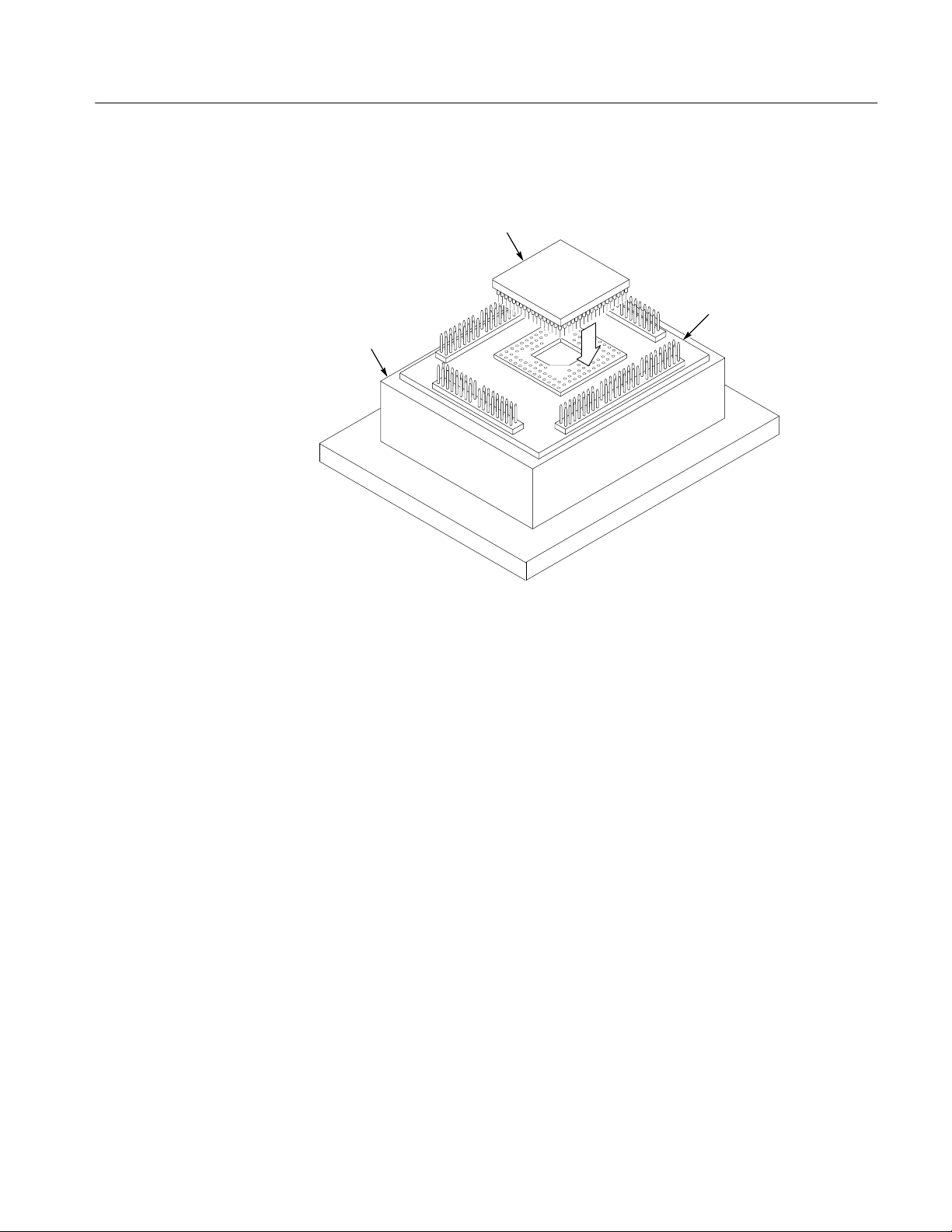
3. Place the probe adapter onto the antistatic shipping foam to support the probe
as shown in Figure 1–4. This prevents the circuit board from flexing and the
socket pins from bending.
4. Remove the microprocessor from your SUT.
5. Line up the pin A1 indicator on the probe adapter board with the pin A1
indicator on the microprocessor.
CAUTION. Failure to correctly place the microprocessor into the probe adapter
might permanently damage the microprocessor once power is applied.
1–6
TMS 260 CPU32 Family Microprocessor Support Instruction Manual
Page 20
Getting Started
6. Place the microprocessor into the probe adapter as shown in Figure 1–4.
Microprocessor
Probe adapter
Foam
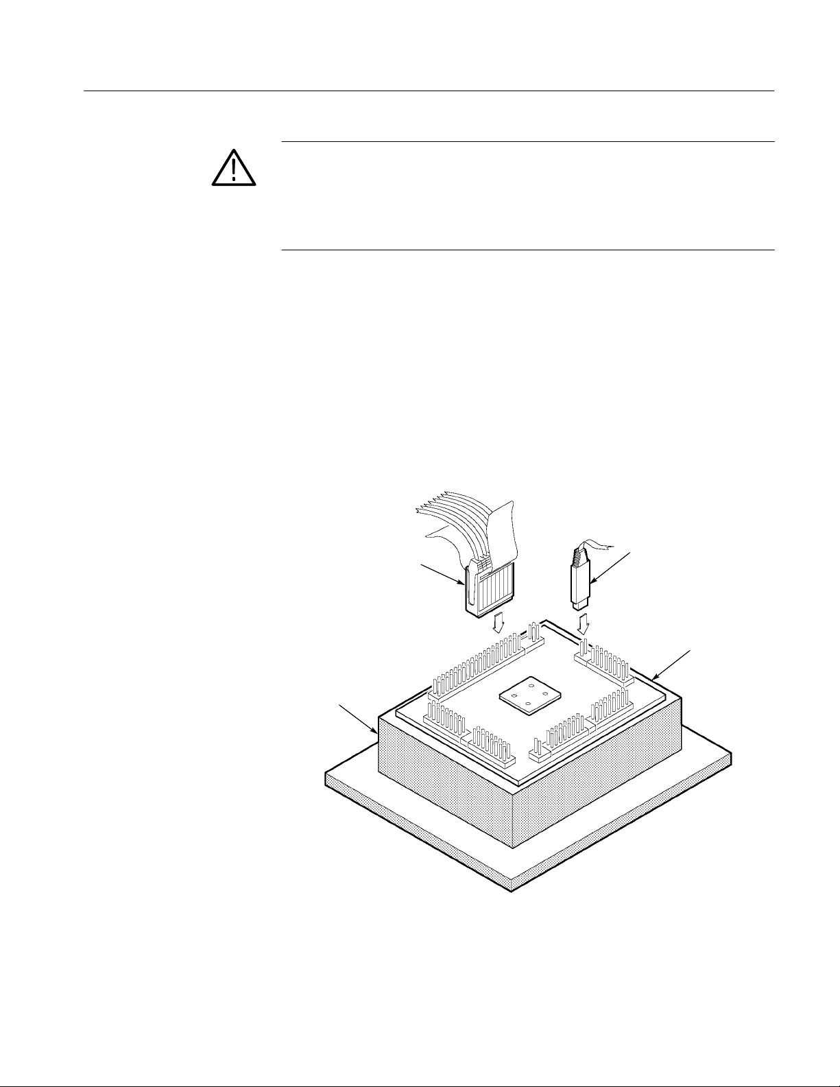
Figure 1–4: Placing a microprocessor into a PGA probe adapter
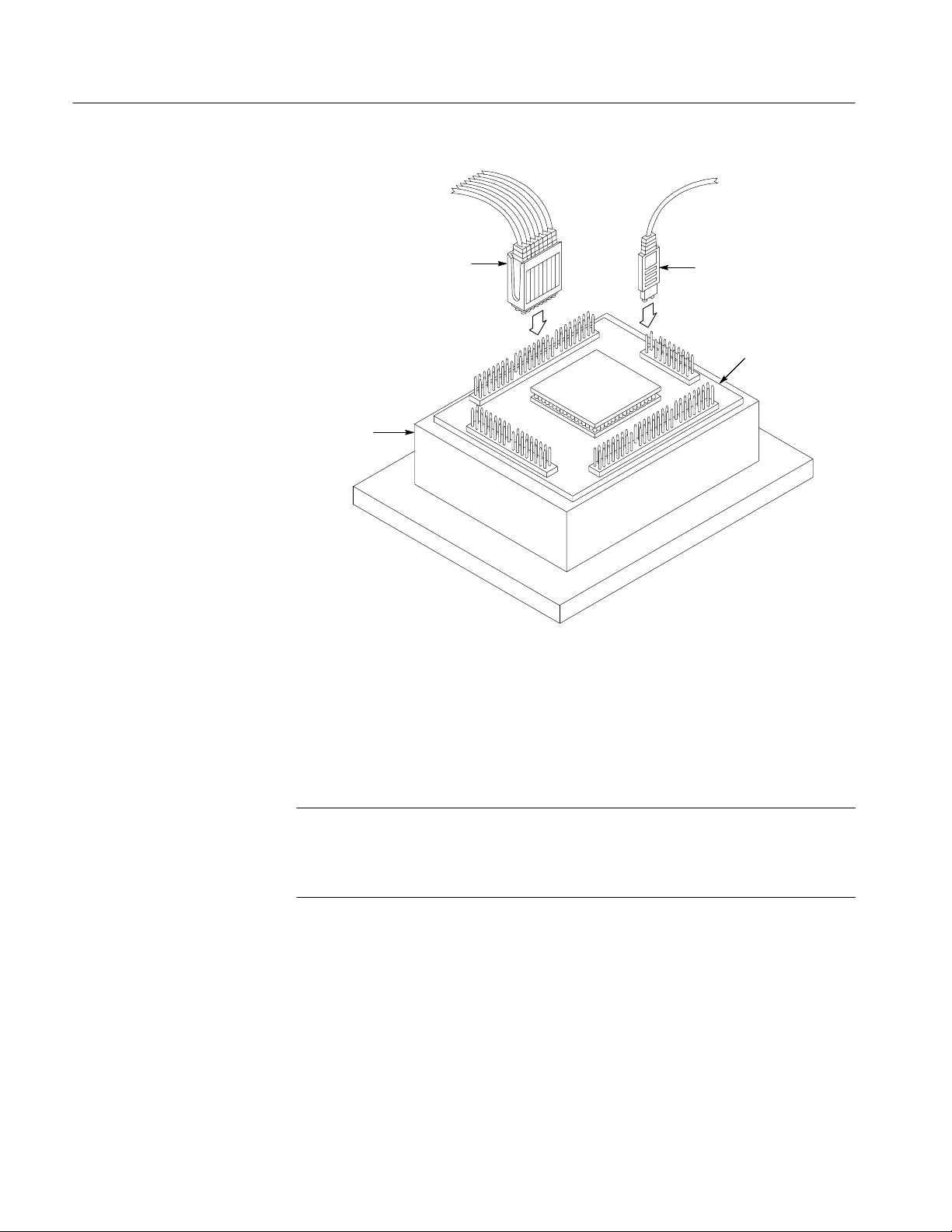
7. Connect the channel and clock probes to the probe adapter as shown in
Figure 1–5. Match the channel groups and numbers on the probe labels to the
corresponding pins on the probe adapter. Match the ground pins on the
probes to the corresponding pins on the probe adapter.
TMS 260 CPU32 Family Microprocessor Support Instruction Manual
1–7
Page 21
Getting Started
Channel probe
Hold the channel probes by the podlet
holder when connecting them to the
probe adapter. Do not hold them by
the cables or necks of the podlets.
Foam
Figure 1–5: Connecting probes to a PGA probe adapter
Clock probe
Probe adapter
8. Line up the pin A1 indicator on the probe adapter board with the pin A1
indicator on your SUT.
9. Place the probe adapter onto the SUT as shown in Figure 1–6.
NOTE. You might need to stack one or more replacement sockets between the SUT
and the probe adapter to provide sufficient vertical clearance from adjacent
components. However, keep in mind that this might increase loading, which can
reduce the electrical performance of your probe adapter.
1–8
TMS 260 CPU32 Family Microprocessor Support Instruction Manual
Page 22

SUT socket
Getting Started
PQFP Probe Adapter
Figure 1–6: Placing a PGA probe adapter onto the SUT
To connect the logic analyzer to the SUT, do the following:
1. Turn off power to your SUT. It is not necessary to turn off the logic analyzer.
CAUTION. Static discharge can damage the microprocessor, the probe adapter,
the podlets, or the module. To prevent static damage, handle all the above only in
a static-free environment.
Always wear a grounding wrist strap or similar device while handling the
microprocessor and probe adapter.
2. To discharge your stored static electricity, touch the ground connector located
on the back of the logic analyzer. Then, touch any of the ground pins of the
probe adapter to discharge stored static electricity from the probe adapter.
3. Place the probe adapter onto the antistatic shipping foam to support the probe
as shown Figure 1–7. This prevents the circuit board from flexing.
TMS 260 CPU32 Family Microprocessor Support Instruction Manual
1–9
Page 23

Getting Started
4. Connect the clock and 8-channel probes to the probe adapter as shown in
Figure 1–7. Match the channel groups and numbers on the probe labels to the
corresponding pins on the probe adapter.
Use leadsets to connect at least one ground lead from each channel probe and
the ground lead from each clock probe to ground pins on your test clip.
Channel probe
Hold the channel probes by the podlet
holder when connecting them to the
probe adapter. Do not hold them by
the cables or necks of the podlets.
Foam
Figure 1–7: Connecting probes to a PQFP probe adapter
Clock probe
Probe adapter
1–10
TMS 260 CPU32 Family Microprocessor Support Instruction Manual
Page 24

Getting Started
CAUTION. This JEDEC
equipped with a clip that has been designed for tight tolerances.
The clip supports only Plastic Quad Flat Pack devices that conform to the
JEDEC M0-069 October 1990 specification. Attaching the clip to a device that
does not conform to this JEDEC standard can easily damage the clip’s connection pins and/or the microprocessor, causing the probe adapter to malfunction.
Please contact your IC manufacturer to verify that the microprocessor you are
targeting conforms to the JEDEC specification.
For best performance and long probe life, exercise extreme care when connecting
the probe to the microprocessor.
5. Line up the pin 1 indicator on the microprocessor with the pin 1 indicator on
the target head of the circuit board.
CAUTION. Failure to correctly place the probe adapter onto the microprocessor
might permanently damage all electrical components when power is applied.
Center the clip on the microprocessor and apply an equal downward force on all
four sides of the clip, slightly rocking the probe adapter in a clockwise circle.
PQFP (Plastic Quad Flat Pack) probe adapter has been
Do not apply leverage to the probe adapter when installing or removing it.
6. Place the probe adapter onto the SUT as shown in Figure 1–8.
TMS 260 CPU32 Family Microprocessor Support Instruction Manual
1–11
Page 25

Getting Started
Microprocessor
CQFP Probe Adapter
Figure 1–8: Placing a PQFP probe adapter onto the SUT
CAUTION. The probe adapter board might slip off or slip to one side of the
microprocessor because of the extra weight of the probes. This can damage the
microprocessor
and the SUT. To prevent this from occurring, stabilize the probe
adapter by placing a non-conductive object (such as foam) between the probe
adapter and the SUT.
To connect the logic analyzer to a SUT using a CQFP probe adapter, follow these
steps:
1. Turn off power to your SUT. It is not necessary to turn off the logic analyzer.
1–12
TMS 260 CPU32 Family Microprocessor Support Instruction Manual
Page 26
Getting Started
CAUTION. Static discharge can damage the microprocessor, the probe adapter,
the probes, or the module. To prevent static damage, handle all the above only in
a static-free environment.
Always wear a grounding wrist strap or similar device while handling the
microprocessor and probe adapter.
2. To discharge your stored static electricity, touch the ground connector located
on the back of the logic analyzer. Then, touch any of the ground pins of the
probe adapter to discharge stored static electricity from the probe adapter.
3. Place the probe adapter onto the antistatic shipping foam to support the probe
as shown Figure 1–9. This prevents the circuit board from flexing.
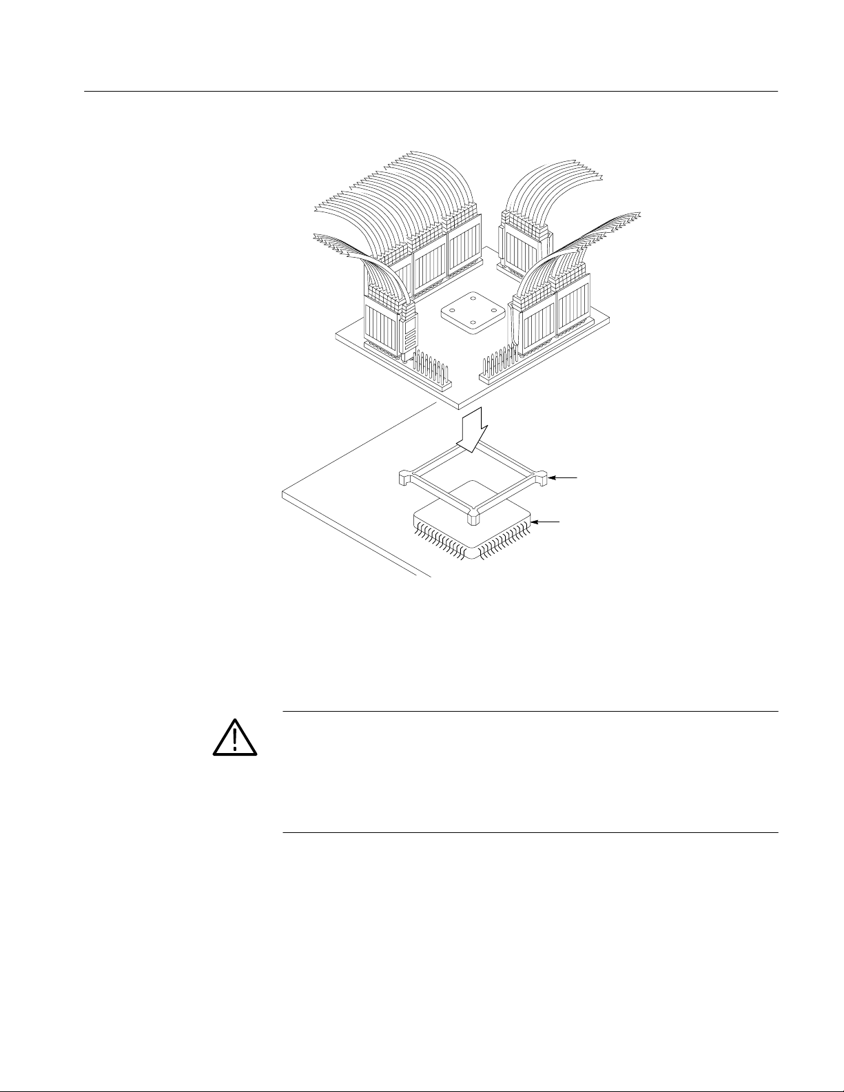
4. Connect the channel and clock probes to the probe adapter as shown in
Figure 1–9. Match the channel groups and numbers on the probe labels to the
corresponding probe adapter pins. Match the ground pins on the probes to the
corresponding pins on the probe adapter.
8-Channel Probe
Hold the 8-Channel Probes by the
podlet holder when connecting them
to the probe adapter. Do not hold
them by the cables or necks of the
podlets.
Foam
Figure 1–9: Connecting probes to a CQFP probe adapter
Clock Probe
Probe Adapter
TMS 260 CPU32 Family Microprocessor Support Instruction Manual
1–13
Page 27

Getting Started
CAUTION. This JEDEC
been equipped with a clip that has been designed for tight tolerances.
The clip supports only Ceramic Quad Flat Pack devices that conform to the
JEDEC M0-069 October 1990 specification. Attaching the clip to a device that
does not conform to this JEDEC standard can easily damage the clip’s connection pins and/or the microprocessor, causing the probe adapter to malfunction.
Please contact your IC manufacturer to verify that the microprocessor you are
targeting conforms to the JEDEC specification.
For best performance and long probe life, exercise extreme care when connecting
the probe adapter to the microprocessor.
5. Place a little glue on each corner of the CQFP-to-PQFP converter.
6. Place the CQFP-to-PQFP converter over your CQFP microprocessor as
shown in Figure 1–10.
NOTE. Do not allow the glue to touch the pins of your microprocessor.
interfere with the connection between the microprocessor and the probe adapter.
An open connection will cause errors.
CQFP (Ceramic Quad Flat Pack) probe adapter has
This might
7. Allow the glue to dry.
1–14
TMS 260 CPU32 Family Microprocessor Support Instruction Manual
Page 28
Converter
Getting Started
Microprocessor
Figure 1–10: Placing a CQFP probe adapter onto the SUT
8. Line up the pin 1 indicator on CQFP clip on the probe adapter with the pin 1
indicator on the microprocessor.
CAUTION. Failure to correctly place the probe adapter onto the microprocessor
might permanently damage all electrical components when power is applied.
Center the clip on the microprocessor and apply an equal downward force on all
four sides of the clip, slightly rocking the probe adapter in a clockwise circle.
Do not apply leverage to the probe adapter when installing or removing it.
9. Place the probe adapter onto the SUT as shown in Figure 1–10.
TMS 260 CPU32 Family Microprocessor Support Instruction Manual
1–15
Page 29

Getting Started
Without a Probe Adapter
You can use channel probes, clock probes, and leadsets with a commercial test
clip (or adapter) to make connections between the logic analyzer and your SUT.
To connect the probes to CPU32 Family signals in the SUT using a test clip,
follow these steps:
1. Turn off power to your SUT. It is not necessary to turn off power to the logic
analyzer.
CAUTION. Static discharge can damage the microprocessor, the probes, or the
module. To prevent static damage, handle all of the above only in a static-free
environment.
Always wear a grounding wrist strap or similar device while handling the
microprocessor.
2. To discharge your stored static electricity, touch the ground connector located
on the back of the logic analyzer. If you are using a test clip, touch any of the
ground pins on the clip to discharge stored static electricity from it.
CAUTION. Failure to place the SUT on a horizontal surface before connecting the
test clip might permanently damage the pins on the microprocessor.
3. Place the SUT on a horizontal static-free surface.
4. Use Table 1–5 to connect the channel probes to CPU32 Family signal pins on
the test clip or in the SUT.
Use leadsets to connect at least one ground lead from each channel probe and
the ground lead from each clock probe to ground pins on your test clip.
5. Align pin 1 or A1 of your test clip with the corresponding pin 1 or A1 of the
CPU32 Family microprocessor in your SUT and attach the clip to the
microprocessor.
T able 1–5: CPU32 Family signal connections for channel probes
Section:channel CPU32 Family signal Section:channel CPU32 Family signal
A3:7 A31 D3:7 D31
A3:6 A30 D3:6 D30
A3:5 A29 D3:5 D29
A3:4 A28 D3:4 D28
A3:3 A27 D3:3 D27
A3:2 A26 D3:2 D26
1–16
TMS 260 CPU32 Family Microprocessor Support Instruction Manual
Page 30

Getting Started
T able 1–5: CPU32 Family signal connections for channel probes (cont.)
Section:channel CPU32 Family signalSection:channelCPU32 Family signal
A3:1 A25 D3:1 D25
A3:0 A24 D3:0 D24
A2:7 A23 D2:7 D23
A2:6 A22 D2:6 D22
A2:5 A21 D2:5 D21
A2:4 A20 D2:4 D20
A2:3 A19 D2:3 D19
A2:2 A18 D2:2 D18
A2:1 A17 D2:1 D17
A2:0 A16 D2:0 D16
A1:7 A15 D1:7 D15
A1:6 A14 D1:6 D14
A1:5 A13 D1:5 D13
A1:4 A12 D1:4 D12
A1:3 A1 1 D1:3 D11
A1:2 A10 D1:2 D10
A1:1 A9 D1:1 D9
A1:0 A8 D1:0 D8
A0:7 A7 D0:7 D7
A0:6 A6 D0:6 D6
A0:5 A5 D0:5 D5
A0:4 A4 D0:4 D4
A0:3 A3 D0:3 D3
A0:2 A2 D0:2 D2
A0:1 A1 D0:1 D1
A0:0 A0 D0:0 D0
C3:7 IFT_NXT_D~ C2:7 RMC~
C3:6 IFETCH_B~ C2:6 BR_D~
C3:5 BKPT~ C2:5 BG_D~
C3:4 CLKOUT_B~ C2:4 BGACK_L~
C3:3 IPP_NXT_D~ C2:3 RESET_L~
C3:2 IPIPE_B~ C2:2 DS~
C3:1 FREEZE C2:1 AS~
C3:0 TSTME_TSC~ C2:0 R_W~
TMS 260 CPU32 Family Microprocessor Support Instruction Manual
1–17
Page 31
Getting Started
T able 1–5: CPU32 Family signal connections for channel probes (cont.)
Section:channel CPU32 Family signalSection:channelCPU32 Family signal
C1:7 not connected C0:7 not connected
C1:6 not connected C0:6 not connected
C1:5 not connected C0:5 not connected
C1:4 not connected C0:4 not connected
C1:3 not connected C0:3 not connected
C1:2 not connected C0:2 not connected
C1:1 not connected C0:1 not connected
C1:0 not connected C0:0 not connected
* Signal not required for disassembly.
Table 1–6 shows the clock probes, and the CPU32 Family signal to which they
must connect for disassembly to be correct.
T able 1–6: CPU32 Family signal connections for clock probes
Section:channel CPU32 Family signal
CK:0 INV_CLKOUT
CK:1 BGACK~_ALT
CK:2 DACK1~
CK:3 DACK2~
1–18
TMS 260 CPU32 Family Microprocessor Support Instruction Manual
Page 32

Setting Up the Support
This section provides information on how to set up the support. Information
covers the following topics:
H Channel group definitions
H Clocking options
H Symbol table files
Remember that the information in this section is specific to the operations and
functions of the TMS 260 CPU32 Family support on any Tektronix logic
analyzer for which it can be purchased. Information on basic operations describes
general tasks and functions.
Before you acquire and disassemble data, you need to load the support and
specify setups for clocking and triggering as described in the information on
basic operations. The support provides default values for each of these setups,
but you can change them as needed.
Channel Group Definitions
Clocking Options
The software automatically defines channel groups for the support. The channel
groups for the CPU32 Family support are Address, Data, Control, DataSize, and
Misc. If you want to know which signal is in which group, refer to the channel
assignment tables beginning on page 3–10.
The TMS 260 support offers a microprocessor-specific clocking mode for the
CPU32 Family microprocessor. This clocking mode is the default selection
whenever you load the CPU32 Family support.
A description of how cycles are sampled by the module using the support and
probe adapter is found in the Specifications chapter.
Disassembly will not be correct with the Internal or External clocking modes.
Information on basic operations describes how to use these clock selections for
general purpose analysis.
The clocking options for the TMS 260 support are: Probe Adapter, Show Cycles,
and Alternate Bus Master Cycles.
TMS 260 CPU32 Family Microprocessor Support Instruction Manual
2–1
Page 33

Setting Up the Support
Probe Adapter
Show Cycles
You can acquire data with or without using the TMS 260 probe adapter.
A Show cycle is defined as any internal bus cycle made visible on the external
bus. These types of cycles are acquired when you select Included.
Alternate Bus Master
Cycles
An alternate bus master cycle is defined as the cycle in which the CPU32 Family
microprocessor gives up the bus to an alternate device (a DMA device or another
microprocessor). These types of cycles are acquired when you select Included.
Symbols
The TMS 260 support supplies one symbol table file. The CPU32 Family_Ctrl
file replaces specific Control channel group values with symbolic values when
Symbolic is the radix for the channel group.
Table 2–1 shows the name, bit pattern, and meaning for the symbols in the file
CPU32 Family_Ctrl, the Control channel group symbol table.
T able 2–1: Control group symbol table definitions
Symbol
RESET
BK_GND_MD
HAL T
BUS_ERROR
AL T_RD
AL T_RD+
AL T_WR
AL T_WR+
AL T_BUS
AL T_BUS+
READ
WRITE
PREFETCH
Control group value
RESET_L~ BG_D~ RMC~ IFETCH_B~
FREEZE BGACK_L~ R_W~ IFT_NXT_D~
AVEC~ BERR~ AS~ IPIPE_B~
IRQ_ANY_D HALT~ DS~ IPP_NXT_D~
Meaning
Reset
Background mode
Halt
Bus error
Alternate bus master read cycle
Alternate bus master read cycle if the
previous cycle was cleared
Alternate bus master write cycle
Alternate bus master write cycle if the
previous cycle was cleared
Any alternate bus master cycle
Any alternate bus master cycle if the
previous cycle was cleared
Read
Write
Read from program space
2–2
TMS 260 CPU32 Family Microprocessor Support Instruction Manual
Page 34

T able 2–1: Control group symbol table definitions (cont.)
Control group value
RESET_L~ BG_D~ RMC~ IFETCH_B~
FREEZE BGACK_L~ R_W~ IFT_NXT_D~
Symbol Meaning
PREFETCH+
SHOW_C_RD
SHOW_C_WR
SHOW_FETH
SHOW_FET+
SH_RMW_RD
SH_RMW_WR
BERR_RTRY*
RMW_READ
RMW_WRITE
RWM*
INT_REQ*
AVEC*
* Symbols used only for triggering; they do not appear in the Disassembly or State displays.
AVEC~ BERR~ AS~ IPIPE_B~
IRQ_ANY_D HALT~ DS~ IPP_NXT_D~
Read from program space if the
previous cycle was cleared
Show cycle read
Show cycle write
Show cycle read from program space
Show cycle read from program space
if the previous cycle was cleared
Show cycle read (RMC cycle)
Show cycle write (RMC cycle)
Bus error retry
Read portion of a Read Modify Write
cycle
Write portion of a Read Modify Write
cycle
Read Modify Write cycle
Interrupt request
Auto vector
Setting Up the Support
Information on basic operations describes how to use symbolic values for
triggering and desplaying other channel groups symbolocally, like the Address
channel group.
TMS 260 CPU32 Family Microprocessor Support Instruction Manual
2–3
Page 35

Acquiring and Viewing Disassembled Data
This section describes how to acquire data and view it disassembled. Information
covers the following topics:
H Acquiring data
H Viewing disassembled data in various display formats
H Cycle type labels
H How to change the way data is displayed
H How to change disassembled cycles with the mark cycles function
Acquiring Data
Once you load the CPU32 Family support, choose a clocking mode and specify
the trigger. You are now ready to acquire disassembled data.
If you have any problems acquiring data, refer to information on basic operations
in your online help or Appendix A: Error Messages and Disassembly Problems in
the basic operations user manual, whichever is available.
Viewing Disassembled Data
You can view disassembled data in four different display formats: Hardware,
Software, Control Flow, and Subroutine. The information on basic operations
describes how to select the disassembly display formats.
NOTE. Selections in the Disassembly property page (the Disassembly Format
Definition overlay) must be set correctly for your acquired data to be disassembled correctly. Refer to Changing How Data is Displayed on page 2–10.
The default display format shows the Address, Data, and Control channel group
values for each sample of acquired data.
The disassembler displays special characters and strings in the instruction
mnemonics to indicate significant events. Table 2–2 shows the special characters
and strings displayed by the CPU32 Family disassembler and gives a definition
of what they represent.
The disassembler will also display * ILLEGAL INSTRUCTION * whenever an
unrecognizable combination of instructions occurs.
TMS 260 CPU32 Family Microprocessor Support Instruction Manual
2–5
Page 36

Acquiring and Viewing Disassembled Data
Asterisks in the Mnemonics column indicate that there is insufficient data
available for complete disassembly of the instruction. The number of asterisks
shows the width of the data that is not available. Two asterisks (**) represent a
byte.
T able 2–2: Meaning if special characters in the display
Character or string displayed Meaning
m The instruction was manually marked as a program fetch
**** Indicates there is insufficient data available for complete
# Indicates an immediate value
t Indicates the number shown is in decimal, such as #12t
* ILLEGAL INSTRUCTION * Decoded as an illegal instruction
A-LINE OPCODE Displayed for an A-Line trap instruction
disassembly of the instruction; the number of asterisks will
indicate the width of the data that is unavailable. Each two
asterisks represent a byte.
F-LINE OPCODE Displayed for an F-Line trap instruction
2–6
TMS 260 CPU32 Family Microprocessor Support Instruction Manual
Page 37

Acquiring and Viewing Disassembled Data
T able 2–3: Cycle Type definitions
Cycle Type Definition
( ALT BUS MASTER: READ ) Another master has control of the bus and is executing a read
cycle
( ALT BUS MASTER: WRITE ) Another master has control of the bus and is executing a
write cycle
( BACKGROUND READ ) A read occurred while the microprocessor was operating in
background mode
( BACKGROUND WRITE ) A write occurred while the microprocessor was operating in
background mode
( BUS ERROR ) External logic aborts current bus cycle
( HALT ) HAL T~ is asserted; microprocessor is halted
( READ ) Data read from memory
( READ RMW ) Read from memory during a read-modify-write cycle
( RESET ) RESET~ is asserted
( SHOW CYCLE READ ) An internal read cycle visible on the bus
( SHOW CYCLE WRITE ) An internal write cycle visible on the bus
( SHOW CYCLE READ RMW ) An internal read cycle visible on the bus and part of a
red-modify-write cycle
( SHOW CYCLE WRITE RMW ) An internal write cycle visible on the bus and part of a
red-modify-write cycle
( UNKNOWN )[
( WRITE ) Data write to memory
( WRITE RMW ) Data write to memory during a read-modify-write cycle
( BREAKPOINT ACK n )* A19-A16 indicate type 0000 where n is the break number
( INT ACK LEVEL: n )* A19-A16 indicate type 111 1 where n is the level number
( INTERNAL REG ACCESS )* A19-A16 indicate type 0011
( FLUSH )[
( READ EXTENSION )[
* Only displayed when FC2-FC0 are available and indicate CPU space.
[ Computed cycle types.
AN unrecognizable combination of control values
Pipeline flush that occurs when the microprocessor branches
to a nonsequential address
Extension fetched from program space
TMS 260 CPU32 Family Microprocessor Support Instruction Manual
2–7
Page 38

Acquiring and Viewing Disassembled Data
Acquiring and Viewing Disassembled Data
1 2 3 4 5 6
Sample Address Data Mnemonic Timestamp
-------------------------------------------------------------------------------35 0000302E 3158 ( EXTENSION ) (S) 180 ns
36 00003030 4879 PEA 000031A4 (S) 180 ns
37 00003032 0000 ( EXTENSION ) (S) 190 ns
38 0000FFB0 0000 ( WRITE ) (S) 170 ns
39 0000FFB2 3158 ( WRITE ) (S) 180 ns
40 00003034 31A4 ( EXTENSION ) (S) 180 ns
41 00003036 0240 ANDI.W #0000,D0 (S) 180 ns
42 00003038 0000 ( EXTENSION ) (S) 180 ns
43 0000FFAC 0000 ( WRITE ) (S) 180 ns
44 0000FFAE 31A4 ( WRITE ) (S) 170 ns
45 0000303A 303C MOVE.W #0001,D0 (S) 190 ns
46 0000303C 0001 ( EXTENSION ) (S) 170 ns
47 0000303E 4EB9 JSR 000030B0 (S) 180 ns
48 00003040 0000 ( EXTENSION ) (S) 180 ns
49 00003042 30B0 ( EXTENSION ) (S) 180 ns
50 00003044 4A40 ( FLUSH ) (S) 180 ns
51 0000FFA8 0000 ( WRITE ) (S) 290 ns
52 0000FFAA 3044 ( WRITE ) (S) 180 ns
53 000030B0 48E7 MOVEM.L A43210/D21,-(A7) (S) 180 ns
54 000030B2 60F8 ( EXTENSION ) (S) 180 ns
55 000030B4 206F MOVEA.L (0030,A7),A0 (S) 180 ns
56 000030B6 0030 ( EXTENSION ) (S) 180 ns
2–8
Figure 2–1: Hardware display
1
Sample Column. Lists logic analyzer memory locations for the acquired
data.
2
Address Group. Lists data from channels connected to the CPU32 Family
Address bus.
3
Data Group. Lists data from channels connected to the CPU32 Family Data
bus.
4
Mnemonics Column. Lists the instructions that have been disassembled.
5
The disassembler displays an (S) or (U) in the mnemonic column to indicate
the mode in which the microprocessor is operating, Supervisor or User. The
FC2-FC0 signals must be valid for the disassembly to recognize these modes.
Figure 2–1 shows the microprocessor operating in Supervisor mode.
6
Timestamp. Lists the timestamp values when a timestamp selection is made
in the Disassembly Format Definition overlay.
TMS 260 CPU32 Family Microprocessor Support Instruction Manual
Page 39

Acquiring and Viewing Disassembled Data
Software Display Format
Control Flow Display
Format
The Software display format shows only the first fetch of executed instructions.
Flushed cycles and extensions are not shown, even though they are part of the
executed instruction. Read extensions will be used to disassemble the instruction,
but will not be displayed as a separate cycle in the Software display format. Data
reads and writes are not displayed.
The disassembler will also display the following cycles or instructions:
H Reset cycle
H Halt cycle
H Bus Error cycle
H Special cycles: Breakpoint Ack, Int Ack, and Internal Reg Access
H Reset Vector
H Reads from the interrupt table that appear due to servicing interrupts
H Illegal instructions
The Control Flow display format shows only the first fetch of instructions that
change the flow of control.
The disassembler will also display the following cycles or instructions:
H Reset cycle
H Halt cycle
H Bus Error cycle
H Special cycles: Breakpoint Ack, Int Ack, and Internal Reg Access
H Reset Vector
H Reads from the interrupt table that appear due to servicing interrupts
H Illegal instructions
Instructions that generate a change in the flow of control in the CPU32 Family
microprocessor are as follows:
Bcc CHK2 JMP RTR
BGND DBcc JSR RTS
BKPT DIVS LPSTOP STOP
BRA DIVSL RESET TRAP
BSR DIVU RTD TRAPcc
CHK DIVUL RTE TRAPV
TMS 260 CPU32 Family Microprocessor Support Instruction Manual
2–9
Page 40

Acquiring and Viewing Disassembled Data
Subroutine Display
Format
The Subroutine display format shows only the first fetch of subroutine call and
return instructions. It will display conditional subroutine calls if they are
considered to be taken.
The Subroutine display format also shows the following cycles:
H Reset Cycle
H Halt Cycle
H Bus Error Cycle
H Special cycles: Breakpoint Ack, Int Ack, Internal Reg Access
H Reset Vector
H Reads from the vector table that appear due to servicing exceptions
H Illegal instructions
H ( UNKNOWN ) cycle types; the disassembler does not recognize the Control
group value
Instructions that generate a subroutine call or a return in the CPU32 Family
microprocessor are as follows:
BGND DIVS LPSTOP RTS
BKPT DIVSL RESET STOP
BSR DIVU RTD TRAP
CHK DIVUL RTE TRAPcc
CHK2 JSR RTR TRAPV
Changing How Data is Displayed
There are fields and features that allow you to further modify displayed data to
suit your needs. You can make selections unique to the CPU32 Family support to
do the following tasks:
H Change how data is displayed across all display formats
H Change the interpretation of disassembled cycles
H Display exception vectors
Optional Display
Selections
You can make optional display selections for disassembled data to help you
analyze the data. You can make these selections in the Disassembly property
page (the Disassembly Format Definition overlay).
2–10
TMS 260 CPU32 Family Microprocessor Support Instruction Manual
Page 41

Acquiring and Viewing Disassembled Data
In addition to the common display options, (described in the information on basic
operations) you can change the displayed data in the following ways:
H Define number of valid address lines
H Define if the FC2–FC0 lines are valid
H Specify the starting address of the interrupt table
H Specify the size of thew interrupt table
The CPU32 Family support has four additional fields: Code Segment Size,
Interrupt Table, Interrupt Table Address, and Interrupt Table Size. These fields
appear in the area indicated in the information on basic operations.
Valid Address Lines. You can select the range of valid address lines used to
disassembly data. The fourteen (14) ranges start with A0–A18 and end with
A0–A31.
The CPU32 Family microprocessor can have an address bus width of 19 to 32
bits, inclusive. There are 14 ranges of valid address bits starting with A0–A18
(default) and ending with A0–A31.
The dissembler ignores upper address bits that fall outside the selected range and
displays them as zero (0).
If you create a symbol table for the address group, be sure that the number of bits
in the symbol table matches the number of valid bits for the address group.
FC2–FC0 Lines Valid. You can choose to use these lines for disassembly by
selecting YES in this field.
The dissembler uses the value of the FC2–FC0 lines to determine if the instruction is from supervisor or user space. The dissembler then displays an S or a U
next to the instruction. CPU space accesses are also displayed.
Vector Base Register. You can specify the base address of the vector register in
hexadecimal. The default hexadecimal base address is 0x00000000.
The dissembler uses the vector base register (VBR) value (the base of the
interrupt table) to compute the name of the interrupt or determine if a conditional
interrupt occurred.
The dissembler ignores upper address bits that fall outside the selected range in
the Valid Address Lines field of the Dissembler Format Definition overlay.
A0 and A0 of the VBR must be set to zero (0).
TMS 260 CPU32 Family Microprocessor Support Instruction Manual
2–11
Page 42

Acquiring and Viewing Disassembled Data
The reset vector information must be located from address 0x0 to 0x7. It does not
matter what the VBR is set to: the dissembler always displays the reset vector at
0 (0x00000000).
Vector Table Size. You can specify the size of the vector table in hexadecimal. The
default vector table size is 0x400.
The dissembler uses the vector table size to compute the name of the interrupt
whenever an exception occurs.
Any value entered in this 12-bit wide field must be divisible by four.
Marking Cycles
Exception Vectors
The disassembler has a Mark Opcode function that allows you to change the
interpretation of a cycle type. Using this function, you can select a cycle and
change it to one of the following cycle types:
H Opcode (the first word of an instruction)
H Extension (a subsequent word of an instruction)
H Flush (an opcode or extension that is fetched but not executed)
Mark selections are as follows:
OPCODE
Ext
Flush
Undo marks on this cycle
Information on basic operations contains more details on marking cycles.
The disassembler can display exception vectors. You can select to display the
interrupt vectors for Real, Virtual, or Protected mode in the Interrupt Table field.
(Selecting Virtual is equivalent to selecting Protected.)
Interrupt cycle types are computed and cannot be used to control triggering.
When the microprocessor processes an interrupt, the disassembler software
displays the type of interrupt, if known.
2–12
You can make these selections in the Disassembly property page (the Disassembly Format Definition overlay).
TMS 260 CPU32 Family Microprocessor Support Instruction Manual
Page 43

Acquiring and Viewing Disassembled Data
Table 2–4 lists CPU32 Family exception vectors.
T able 2–4: Interrupt vectors
Vector
Number
0 ( RESET: STACK POINTER )
1 ( RESET: PROGRAM COUNTER )
2 ( BUS ERROR VECTOR )
3 ( ADDRESS ERROR VECTOR )
4 ( ILLEGAL INSTRUCTION VECTOR )
5 ( ZERO DIVIDE VECTOR )
6 ( CHK, CHK2 VECTOR )
7 ( TRAPcc, TRAPV VECTOR )
8 ( PRIV VIOLATION VECT OR )
Displayed interrupt name
9 ( TRACE VECTOR )
10 ( LINE 1010 EMULATOR VECT OR )
11 ( LINE 1111 EMULAT OR VECTOR )
12 ( HARDWARE BREAKPOINT VECTOR )
13 ( RESERVED VECTOR #13t )
14 ( FORMAT ERROR VECTOR )
15 ( UNINIT INTERRUPT VECTOR )
16-23 ( RESERVED VECTOR #16t–#23t )
24 ( SPURIOUS INTERRUPT VECTOR )
25 ( IPL 1 AUTOVECTOR )
26 ( IPL 2 AUTOVECTOR )
27 ( IPL 3 AUTOVECTOR )
28 ( IPL 4 AUTOVECTOR )
29 ( IPL 5 AUTOVECTOR )
30 ( IPL 6 AUTOVECTOR )
31 ( IPL 7 AUTOVECTOR )
32-47 ( TRAP #0t–#15t VECTOR )
48-63 ( RESERVED VECTOR #48t–#63t )
64-255 ( USER INT VECTOR )
TMS 260 CPU32 Family Microprocessor Support Instruction Manual
2–13
Page 44

Acquiring and Viewing Disassembled Data
Viewing an Example of Disassembled Data
A demonstration system file (or demonstration reference memory) is provided so
you can see an example of how your CPU32 Family microprocessor bus cycles
and instruction mnemonics look when they are disassembled. Viewing the system
file is not a requirement for preparing the module for use and you can view it
without connecting the logic analyzer to your SUT.
Information on basic operations describes how to view the file.
2–14
TMS 260 CPU32 Family Microprocessor Support Instruction Manual
Page 45

Specifications
This chapter contains the following information:
H Probe adapter description
H Specification tables
H Dimensions of the probe adapter
H Channel assignment tables
H Description of how the module acquires CPU32 Family signals
H List of other accessible CPU32 Family signals and extra acquisition channels
Probe Adapter Description
The probe adapter is nonintrusive hardware that allows the logic analyzer to
acquire data from a CPU32 Family microprocessor in its own operating
environment with little effect, if any, on that system. Information on basic
operations contains a figure showing the logic analyzer connected to a typical
probe adapter. Refer to that figure while reading the following description.
Configuring the Probe
Adapter
The probe adapter consists of a circuit board and a socket for a CPU32 Family
microprocessor. The probe adapter connects to the microprocessor in the SUT.
Signals from the microprocessor-based system flow from the probe adapter to the
channel groups and through the probe signal leads to the module.
All circuitry on the probe adapter is powered from the SUT.
Circuitry on the probe adapter can be powered from either the SUT or an external
power source. Refer to Applying and Removing Power in the Getting Started
chapter for information on using an external power source.
The PGA probe adapter accommodates the Motorola 68340 microprocessor in a
145-pin PGA package.
The PQFP probe adapter accommodates the Motorola 68340 microprocessor in a
145-pin PQFP or CQFP packages.
The Evaluation Board probe adapter accommodates the Motorola
M68331/68332EVS evaluation board.
The standard 68331/332 QFP probe adapter, optional 68340 PGA probe adapter
and optional 68331/332 Motorola evaluation system board adapter contain
TMS 260 CPU32 Family Microprocessor Support Instruction Manual
3–1
Page 46

Specifications
Jumpe
Jumpe
Jumpe
jumpers that need to be in specific positions for proper disassembly. Tables 3–1,
3–2, and 3–3, show these positions.
T able 3–1: 68331/332 QFP probe adapter jumper positions
Jumper position
r
A19-A23 pins 1, 2 (Gnd)* pins 2, 3 (Address)
BGACK~ pins 1, 2 (High) pins 2, 3 (BGACK~)
BG~ pins 1, 2 (High) pins 2, 3 (BG~)
BR~ pins 1, 2 (High) pins 2, 3 (BR~)
* The podlets are grounded on the probe adapter only; the microproces-
sor signals are not affected.
Default
Alternate
T able 3–2: 68340 PGA probe adapter jumper positions
Jumper position
r
A31-A24 pins 1, 2 (Gnd)* pins 2, 3 (future)
* The podlets are grounded on the probe adapter only; the microproces-
sor signals are not affected.
Default
Alternate
T able 3–3: 68331/332 evaluation board probe adapter jumper
positions
3–2
Jumper position
r
A31-A24 pins 1, 2 (Gnd)* none
A23-A19 pins 1, 3 (Gnd)* pins 3, 5 (Address)
DACK1~ pins 1, 2 (High) none
DACK2~ pins 1, 2 (High) none
BGACK~ pins 1, 3 (High) pins 3, 5 (CS2~)
BG~ pins 1, 2 (High) pins 2, 3 (BG~)
BR~ pins 1, 2 (High) pins 2, 3 (BR~)
* The podlets are grounded on the probe adapter only; the microproces-
sor signals are not affected.
Default
Alternate
TMS 260 CPU32 Family Microprocessor Support Instruction Manual
Page 47

Specifications
Figure 3–1 shows the location of the jumpers on the 68331/332 QFP probe
adapter.
BGACK~
BG~
A20
A22
A30
A28
A26
A24
BR~
A19
A21
A23
Figure 3–1: Jumper locations on the 68331/332 QFP probe adapter
Figure 3–2 shows the location of the jumpers on the 68340 PGA probe adapter.
A31
A29
A27
A25
Figure 3–2: Jumper locations on the 68340 PGA probe adapter
TMS 260 CPU32 Family Microprocessor Support Instruction Manual
3–3
Page 48

Specifications
Figure 3–3 shows the location of the jumpers on the 68331/332 Evaluation Board
probe adapter.
A25
A27
A29
A31
A24
A26
A28
A30
A20
A21
A22
A23
A19 BG~ BR~ BGACK~
DACK1~DACK2~
Specifications
3–4
Figure 3–3: Jumper locations on the 68331/332 Evaluation Board probe adapter
These specifications are for a probe adapter connected to a compatible Tektronix
logic analyzer, and the SUT. Table 3–4 shows the electrical requirements the
SUT must produce for the support to acquire correct data.
In Table 3–4, for the 102-channel module, one podlet load is 20 k in parallel
with 2 pF. For the 96-channel module, one podlet load is 100 k in parallel with
10 pF. For the 80 channel module, one podlet load is 100 k in parallel with
5 pF.
TMS 260 CPU32 Family Microprocessor Support Instruction Manual
Page 49

Specifications
T able 3–4: Electrical specifications
Characteristics Requirements
SUT DC power requirements
Voltage 4.75-5.25 VDC
Current I max (calculated) 102 mA
I typ (measured) 55 mA
SUT clock Min DC
Clock rate Max. 16.78 MHz
Minimum setup time required
All signals 4 ns
Minimum hold time required
All signals 3 ns
Specification
Measured typical SUT signal loading AC load DC load
CLKOUT 8 pF + 1 podlet 74AS1000
A31–A23 17 pF + 1 podlet 1 podlet
BG~ 15 pF + 1 podlet 74AS1000 in par-
allel with 1 podlet
(74AC20 on op-
tion 1A board)
BGACK~ 12 pF 74F174
RESET~ 12 pF + 1 podlet 74F174
IRQ~ 11 pF 74F30
(74AC20 on op-
tion 1A board)
IFETCH~ 10 pF + 1 podlet 74AS1034 in par-
allel with 1 podlet
IPIPE~ 10 pF + 1 podlet 74AS1034 in par-
FREEZE 9 pF + 1 podlet 1 podlet
BKPT 9 pF + 1 podlet 1 podlet
All other signals 7 pF + 1 podlet 1 podlet
TMS 260 CPU32 Family Microprocessor Support Instruction Manual
allel with 1 podlet
3–5
Page 50

Specifications
Table 3–5 shows the environmental specifications.
T able 3–5: Environmental specification*
Characteristic Description
Temperature
Maximum operating
Minimum operating 0°C (+32°F)
Non-operating –55°C to +75°C (–67°F to +167°F)
Humidity 10% to 95% relative humidity*
Altitude
Operating 4.5 km (15,000 ft) maximum
Non-operating 15 km (50,000 ft) maximum
Electrostatic immunity The probe adapter is static sensitive
* Designed to meet Tektronix standard 062-2847-00 class 5.
[
Not to exceed CPU32 Family microprocessor thermal considerations. Forced air
cooling might be required across the CPU.
+50°C (+122°F)[
3–6
TMS 260 CPU32 Family Microprocessor Support Instruction Manual
Page 51
Specifications
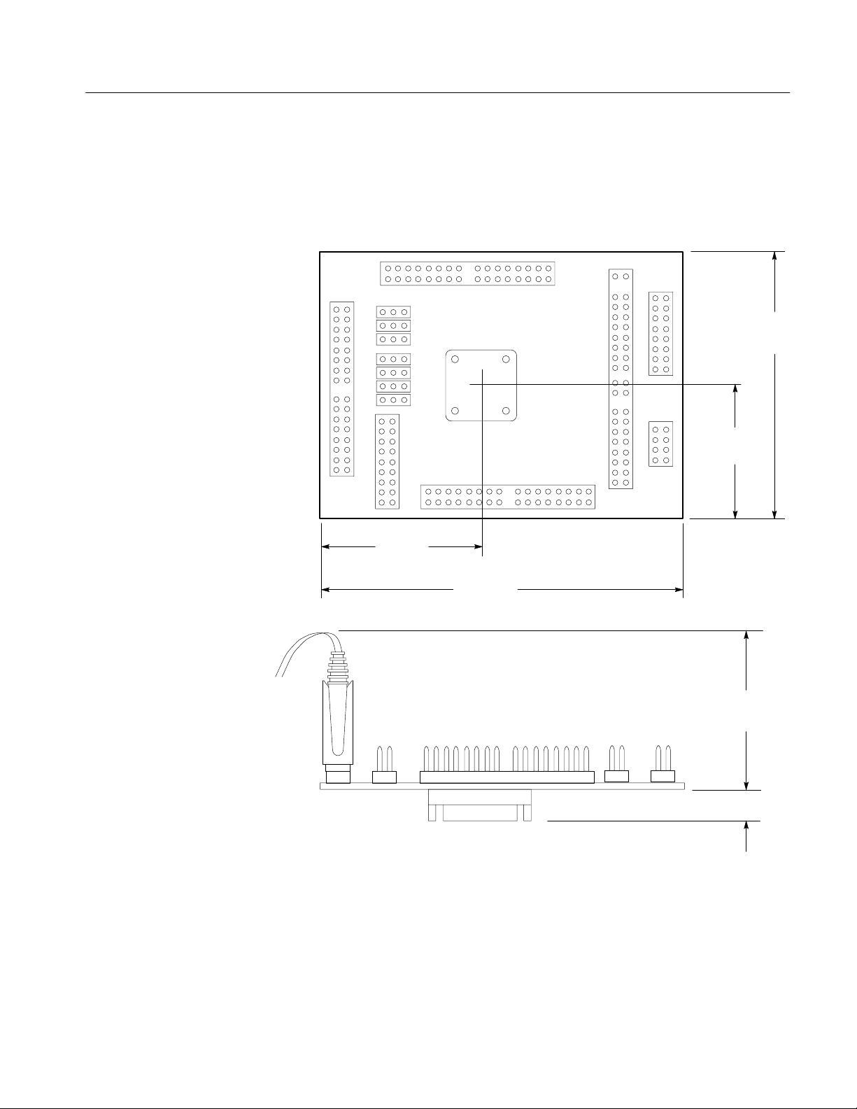
Figures 3–4, 3–5, and 3–6 show the dimensions of the probe adapters with the
podlet attached. Figure 3–4 shows the standard 68331/332 QFP probe adapter;
Figure 3–5 shows the 68340 PGA probe adapter. Figure 3–6 shows the
68331/332 Evaluation Board probe adapter.
67 mm
(2.65 in)
33.mm
(1.3 in)
52 mm
(2.05 in)
91 mm
(3.6 in)
Figure 3–4: Minimum clearance of the 68331/332 QFP probe adapter
43 mm
(1.7
in)
12 mm
(.46 in)
TMS 260 CPU32 Family Microprocessor Support Instruction Manual
3–7
Page 52

Specifications
66 mm
(2.60 in)
PIN
1
14 mm
(.57 in)
18 mm
(.73 in)
96 mm
(3.80 in)
43 mm
(1.7 in)
7 mm
(.26 in)
Figure 3–5: Minimum clearance of the 68340 PGA probe adapter
3–8
TMS 260 CPU32 Family Microprocessor Support Instruction Manual
Page 53

Specifications
83 mm
(3.30 in)
95 mm
(3.75 in)
43 mm
(1.7 in)
13 mm
(.53 in)
Figure 3–6: Minimum clearance of the 68331/332 evaluation board probe adapter
TMS 260 CPU32 Family Microprocessor Support Instruction Manual
3–9
Page 54

Specifications
Table 3–6 shows the certifications and compliances that apply to the probe
adapter.
T able 3–6: Certifications and compliances
EMC Compliance Meets the intent of Directive 89/336/EEC for Electromagnetic Compatibility when it is used with the
product(s) stated in the specifications table. Refer to the EMC specification published for the stated
products. May not meet the intent of the Directive if used with other products.
FCC Compliance Emissions comply with FCC Code of Federal Regulations 47, Part 15, Subpart B, Class A Limits
Approvals ANSI/ISA S82.01 – Safety standard for electrical and electronic test, measuring, controlling, and
related equipment, 1994
UL31 11-1 – Standard for electrical measuring and test equipment
CAN/CSA C22.2 No. 1010.1 – Safety requirements for electrical equipment for measurement,
control and laboratory use
IEC1010-1 – Safety requirements for electrical equipment for measurement, control, and laboratory
use
Channel Assignments
Channel assignments shown in Table 3–7 through Table 3–12 use the following
conventions:
H All signals are required by the support unless indicated otherwise
H Channels are shown starting with the most significant bit (MSB) descending
to the least significant bit (LSB)
H Channel group assignments are for all modules unless otherwise noted
H A tilde (~) following a signal name indicates an active low signal
H An equals sign (=) following a signal name indicates that it is double probed
Table 3–7 shows the probe section and channel assignments for the Address
group, and the microprocessor signal to which each channel connects. By default
this channel group is displayed in hexadecimal.
T able 3–7: Address group channel assignments
CPU32 Family signal
Bit order Section:channel
31 A3:7
30 A3:6
29 A3:5
28 A3:4
27 A3:3
26 A3:2
name
A31_D*[
A30_D*[
A29_D*[
A28_D*[
A27_D*[
A26_D*[
3–10
TMS 260 CPU32 Family Microprocessor Support Instruction Manual
Page 55

T able 3–7: Address group channel assignments (cont.)
CPU32 Family signal
Bit order
25 A3:1
24 A3:0
23 A2:7 A23_D*
22 A2:6 A22_D*
21 A2:5 A21_D*
20 A2:4 A20_D*
19 A2:3 A19_D*
18 A2:2 A18
17 A2:1 A17
16 A2:0 A16
15 A1:7 A15
14 A1:6 A14
13 A1:5 A13
12 A1:4 A12
11 A1:3 A1 1
10 A1:2 A10
9 A1:1 A9
8 A1:0 A8
7 A0:7 A7
6 A0:6 A6
5 A0:5 A5
4 A0:4 A4
3 A0:3 A3
2 A0:2 A2
1 A0:1 A1
0 A0:0 A0
[
When acquiring data with the QFP probe adapter or
without a probe adapter, these signals must be tied to
ground. On the probe adapter position the jumpers
associated with A31-A24 on pins 1 and 2.
Section:channel
name
A25_D*[
A24_D*[
Specifications
* Signals only used for disassembly when within the range
of valid upper address bits selected in the Disassembly
property page for the 102-channel module, or in the
Disassembly Format Definition overlay for the 96-channel
module. Upper address bits outside the selected range
are ignored.
TMS 260 CPU32 Family Microprocessor Support Instruction Manual
3–11
Page 56

Specifications
Table 3–8 shows the probe section and channel assignments for the Data group,
and the microprocessor signal to which each channel connects. By default this
channel group is displayed in hexadecimal.
T able 3–8: Data group channel assignments
Bit
order
15 D1:7 D15
14 D1:6 D14
13 D1:5 D13
12 D1:4 D12
11 D1:3 D11
10 D1:2 D10
9 D1:1 D9
8 D1:0 D8
7 D0:7 D7
6 D0:6 D6
5 D0:5 D5
4 D0:4 D4
3 D0:3 D3
2 D0:2 D2
1 D0:1 D1
0 D0:0 D0
Section:channel
CPU32 Family signal
name
3–12
Table 3–9 shows the probe section and channel assignments for the Control
group, and the microprocessor signal to which each channel connects. By default
this channel group is displayed symbolically
T able 3–9: Control group channel assignments
Bit
order
15 C2:3 RESET_L~
14 C3:1 FREEZE
13 D2:5
12 D2:2
11 C2:5 BG_D~
10 C2:4 BGACK_L~
9 D2:1 BERR~
8 D2:0 HALT~
Section:channel CPU32 Family signal name
AVEC~ *
IRQ_ANY_D *
[
}
§
§
TMS 260 CPU32 Family Microprocessor Support Instruction Manual
Page 57

T able 3–9: Control group channel assignments (cont.)
Bit
order
7 C2:7 RMC~
6 C2:0 R_W~
5 C2:1 AS~
4 C2:2 DS~
3 C3:6 IFETCH_B~
2 C3:7 IFT_NXT_D~ #
1 C3:2 IPIPE_B~ *
0 C3:3 IPP_NXT_D~ *#
* Signals not required for disassembly.
[
When acquiring data with the PGA probe adapter or without a
probe adapter, pull high if the port is set up for CS0~ (not AVEC~).
}
When acquiring data without a probe adapter, pull low or connect
to any inverted IRQ line.
§
When acquiring data without a probe adapter, pull high if not used
or used as a chip select signal.
CPU32 Family signal nameSection:channel
Specifications
# When acquiring data without a probe adapter, connect IFETCH* to
both C3:6 & C3:7 podlets. Also connect IPIPEX to both C3:2 & C3:3
podlets.
Table 3–10 shows the probe section and channel assignments for the DataSize
group, and the microprocessor signal to which each channel connects. By default
this channel group is displayed symbolically.
T able 3–10: DataSize group channel assignments
Bit
order
7 D3:3 FC3
6 D3:2 FC2
5 D3:1 FC1
4 D3:0 FC0
3 D2:6 DSACK1~ *
2 D2:7 DSACK0~ *
1 D2:3 SIZ1
0 D2:4 SIZ0
* Signals not required for disassembly.
Section:channel CPU32 Family signal name
TMS 260 CPU32 Family Microprocessor Support Instruction Manual
3–13
Page 58
Specifications
Table 3–11 shows the probe section and channel assignments for the Misc group,
and the microprocessor signal to which each channel connects. By default this
channel group is displayed symbolically.
T able 3–11: Misc group channel assignments
Bit
order
4 C3:5 BKPT~ *
3 C2:6
2 C3:0 TSTME_TSC *
1 D3:4 CSBOOT~ *
0 C3:4 CLKOUT_B *
* Signal not required for disassembly.
[
Section:channel CPU32 Family signal name
BR_D~ *
When acquiring data with the PGA probe adapter or without a
probe adapter, pull high if the port is set up for CS0~ (not AVEC~).
[
How Data is Acquired
Table 3–12 shows the probe section and channel assignments for the clock probes
(not part of any group), and the CPU32 Family signal to which each channel
connects.
T able 3–12: Clock channel assignments
CPU32 Family signal
Section:channel
CK:3 DACK2~
CK:2 DACK1~
CK:1 BGACK~_ALT
CK:0 INV_CLKOUT
name
The channels in Table 3–12 are used only to clock in data. These channels are not
acquired or displayed. To acquire data from any of the signals shown in Table
3–12, you must connect another channel probe to the signal. This technique is
called double probing. An equals sign (=) following a signal name indicates that
it is already double probed.
3–14
This part of this chapter explains how the module acquires CPU32 Family
signals using the TMS 260 support and probe adapter. This part also provides
additional information on microprocessor signals accessible on or not accessible
TMS 260 CPU32 Family Microprocessor Support Instruction Manual
Page 59

Specifications
on the probe adapter, and on extra acquisition channels available for you to use
for additional connections.
Custom Clocking
A special clocking program is loaded to the module every time you select the
microprocessor support. This special clocking is called Custom.
With Custom clocking, the module logs in signals from multiple groups of
channels at different times as they become valid on the CPU32 Family bus. The
module then sends all the logged-in signals to the trigger machine and to the
acquisition memory of the module for storage.
In Custom clocking, the module clocking state machine (CSM) generates one
master sample for each CPU32 Family bus cycle, no matter how many clock
cycles are contained in the bus cycle. The CSM accommodates bus cycles with
an arbitrary number of wait states, including zero.
Figure 3–7 shows the sample points and the master sample point.
A normal bus cycle begins when AS~ becomes low. All signals are then logged,
and the CSM enters the BUS_START state. One of the following options then
occurs:
H If AS~ becomes high on the next cycle (a fast bus cycle lasting two clock
cycles), Address and some control signals are logged in again and a master
strobe is executed. This way, information on the IFETCH~ and IPIPE~ lines
is not overwritten.
H If AS~ remains low on the next cycle, all signals are logged again and the
CSM enters the BUS_CONT state. While the CSM remains in this state, only
the information from sample point 2 is logged, and is logged repetitively on
every CLK cycle. This avoids overwriting information on the IFETCH and
IPIPE lines. When AS~ becomes high again, a Master strobe sends the
logged information to the PRISM.
If ALT_BUS_D becomes high at any time, logging of BG~ and BGACK~ stops.
Consequently, if BG~ becomes true during a regular bus cycle, it is not recorded.
TMS 260 CPU32 Family Microprocessor Support Instruction Manual
3–15
Page 60

Specifications
S0 S1 S2 S3 S5
CLKOUT
INV
CLKOUT
AS~
Address
Data
Sample
point 1
[Channels not set up in a channel group by the TMS 260 software are logged with the Master sample.
S4 S6
Sample
point 2
Master
Sample
Figure 3–7: CPU32 Family bus timing for a normal Read/Write cycle
Sample point 1 includes A23-A0, IPIPE~, IFETCH~, BR_D~, DS~, and
RESET_L~.
Master sample point[
point
Sample point 2 includes D15-D0, IFT_NXT_D~,IPP_NXT_D~, DSACK0~,
DSACK1~, AVEC~, SIZ0, SIZ1, IRQ_ANY_D, BERR~, HALT~,CSBOOT~,
FC2-FC0, TSTME~_TSC, RMC~, R_W~,BKPT~, BG_D~, FREEZE,
AS~,BGACK_L~, and CLKOUT_B.
3–16
TMS 260 CPU32 Family Microprocessor Support Instruction Manual
Page 61

Specifications
Figure 3–8 shows the sample points and the master sample for a Show bus cycle.
A Show cycle is any internal bus cycle made visible on the external bus. These
cycles are characterized by the AS~ signal remaining high while the DS~ signal
is asserted. Show cycles are made visible by writing to a register in the microprocessor. Micro clocking includes these cycles by default, but a selection on the
Clock Menu allows you to exclude them. As with normal cycles, if the
BGACK~_ALT signal becomes true, the BG~ and BGACK~ signals are no
longer logged in.
S0 S1
CLKOUT
INV
CLKOUT
DS~
Address
Data
Sample
point 1
S0 S2
Sample
point 2
Master
sample
point
Figure 3–8: CPU32 Family bus timing for a Show Bus cycle
Sample point 1 includes A23-A0, IPIPE~, IFETCH~, BR_D~, DS~, and
RESET_L~.
Sample point 2 includes D15-D0, IFT_NXT_D~,IPP_NXT_D~, DSACK0~,
DSACK1~, AVEC~, SIZ0, SIZ1, IRQ_ANY_D, BERR~, HALT~,CSBOOT~,
FC2-FC0, TSTME~_TSC, RMC~, R_W~,BKPT~, BG_D~, FREEZE,
AS~,BGACK_L~, and CLKOUT_B.
Alternate Bus Master cycles are not normally acquired. You can include these
cycles in the Alternate Bus Master Cycles field in the custom clocking dialog for
the 102-channel module or in the Custom Clock Setup menu for the 96-channel
module.
When ALT_BUS_D is sensed as high, the CSM goes to the DUMB_IDLE state
(except during a regular cycle, in which case the CSM logs the current cycle
before entering the DUMB_IDLE state). In the DUMB_IDLE state, the CSM
waits for strobes AS~ or DS~ to go active, then logs a normal bus cycle or a
show cycle, respectively. If neither strobe becomes active but ALT_BUS_D is
TMS 260 CPU32 Family Microprocessor Support Instruction Manual
3–17
Page 62

Specifications
deasserted, a bus cycle is sent with the signal logged on the previous clock edge.
Otherwise, all bus cycles are logged in using the same method as regular cycles.
Clocking Options
The clocking algorithm for the CPU32 Family support has two variations:
Alternate Bus Master Cycles Excluded, and Alternate Bus Master Cycles
Included.
Probe Adapter. With normal bus cycles, there are two sample points, of which the
second sample point is also the master sample. Figures 3–7 and 3–8 show these
sample points.
Without Probe Adapter. When no probe adapter is used, all data is logged in at the
master sample point shown in Figures 3–7 and 3–8.
Show Cycles Included. With Show cycles included, there are two sample points,
of which the second sample point is also the master sample. Figure 3–8 shows
these sample points.
Show Cycles Excluded. Show cycle data is ignored, not acquired.
Alternate Bus Master Cycles Excluded. Alternate bus master cycles are not logged
in.
Alternate Bus Master Cycles Included. All bus cycles, including Alternate Bus
Master cycles, are logged in. If either BG~ or BGACK~ are true (signals
selectable with jumpers on the probe adapter), the bus cycle will be considered
an alternate bus master cycle. To log in these cycles, the DS~ or AS~ signals
must also be active true.
When the BOFF# signal goes low (active), a backoff cycle has been requested,
and the CPU32 Family microprocessor gives up the bus on the next clock cycle.
The module aborts the bus cycle that it is currently logging in (the CPU32
Family microprocessor will restart this cycle once the BOFF# signal goes high).
A backoff cycle will be logged in using one of the three interactions described
for the HLDA signal (except that the BOFF# signal is stored as a low-level signal
in each of the cases).
H If the alternate bus master drives the same control lines as the CPU32 Family
microprocessor, and the CPU32 Family microprocessor “sees” these signals,
the bus activity is logged in like normal bus cycles except that the BG~ or
BGACK~ signal is low.
H If none of the control lines are driven or if the CPU32 Family microprocessor
can not see them, the module will still clock in an alternate bus master cycle.
3–18
TMS 260 CPU32 Family Microprocessor Support Instruction Manual
Page 63

The information on the bus, one clock prior to the BG~ or BGACK~ signal
going high is logged in.
H If some of the CPU32 Family microprocessor control lines are visible (but
not all), the module logs in what it determines is valid from the control
signals and logs in the remaining bus signals one clock cycle prior to the
BG~ or BGACK~ signal going high.
Alternate Microprocessor Connections
For a list of signals required or not required for disassembly, refer to the channel
assignment tables beginning on page 3–10. Remember that these channels are
already included in a channel group. If you connect extra these channels to other
signals, you should set up another channel group for them.
Specifications
Signals On the Probe
Adapter
The probe adapter board contains pins for microprocessor signals that are not
acquired by the TMS 260 support. You can connect extra channels to these pins,
because they can be useful for general purpose analysis.
These channels are not defined as a channel group and data acquired from them
is not displayed. To display data you will need to define a channel group.
Table 3–13 shows the microprocessor signals available on J1612 of the probe
adapter.
T able 3–13: CPU32 Family signals on J1612
Pin
No.
CPU32 Family signal name
68331 68332 68331 68332
1 GND GND 10 OC4 TP8
2 PCLK T2CLK 11 NC TP7
3 PWMB TP15 12 OC3 TP6
4 PWMA TP14 13 OC2 TP5
5 NC TP13 14 OC1 TP4
6 NC TP12 15 IC3 TP3
7 NC TP11 16 IC2 TP2
8 PAI TP10 17 IC1 TP1
9 IC4/OC5 TP9 18 NC TP0
Pin
No.
CPU32 Family signal name
Signals Not On the Probe
Adapter
The probe adapter does not provide access for the following microprocessor
signals:
TMS 260 CPU32 Family Microprocessor Support Instruction Manual
3–19
Page 64

Specifications
EXTAL MOSI PCS2~ SCK VSTBY*
MISO PCS0~/SS~ PCS3~ TXD XFC
MODCLK PCS1~ RXD VDDSYN XTAL
The following is a list of microprocessor signals that are not accessible on the
68340 PGA probe adapter.
CS1~ DREQ1~ RXDB TGATE2~ TXDB
CS2~ DREQ2~ RXRDYA TIN1 TXRDYA
CS3~ EXTAL SCLK TIN2 X1
CTSA~ MODCK TCK TMS X2
CTSB~ RTSA~ TD0 TOUT1 XFC
DONE1~ RTSB~ TD1 TOUT2 XTAL
DONE2~ RXDA TGATE1 TXDA VCCSYN
Extra Channels
Table 3–14 lists extra sections and channels that are left after you have connected
all the probes used by the support. You can use these extra channels to make
alternate SUT connections.
T able 3–14: Extra module sections and channels
Module Section: channels
102-channels C1:7-0, C0:7-0
136-channels C1:7-0, C0:7-0, E3:7-0, E2:7-0, E1:7-0, E0:7-0
96-channels C1:7-0, C0:7-0
These channels are not defined in any channel group and data acquired from
them is not displayed. To display data, you will need to define a channel group.
3–20
TMS 260 CPU32 Family Microprocessor Support Instruction Manual
Page 65

WARNING
The following servicing instructions are for use only by qualified personnel. To
avoid injury, do not perform any servicing other than that stated in the operating
instructions unless you are qualified to do so. Refer to all Safety Summaries
before performing any service.
Page 66

Maintenance
This section contains information on the following topics:
H Probe adapter circuit description
Probe Adapter Circuit Description
The QFP probe adapter board and Evaluation Board Adapter board have the
same circuitry (except that the 74F30 on the QFP probe adapter is replaced by a
74AC20 on the Evaluation Board probe adapter). The CLKOUT signal goes to
the acquisition module after being inverted. The inverted clock also latches the
asynchronous signals BGACK~ and RESET~ to avoid metastables going into the
Clocking State Machine. The IFETCH~ and IPIPE~ lines are buffered through a
74AS1034 to minimize loading.
BG~ and BGACK_L~ (and DACK1~ and DACK2~ on the option 1A board) are
combined to form a signal called ALT_BUS_D. When this is high, the processor
has given up the bus. Similarly, all the IRQ~s (IRQ3~, IRQ5~, IRQ6~, and
IRQ7~ on the option 1A board) are OR’ed together to form a signal called
IRQ_ANY_D that, when high, indicates an interrupt request is active.
All other acquired signals go directly to the logic analyzer podlets.
J1771 and J1671 are used to turn off the cache. The SUT drives these lines,
therefore the SUT driver must be disabled to use this option.
Replacing Signal Leads
Information on basic operations describes how to replace signal leads (individual
channel and clock probes).
Replacing Protective Sockets
Information on basic operations describes how to replace protective sockets.
TMS 260 CPU32 Family Microprocessor Support Instruction Manual
4–1
Page 67

Replaceable Electrical Parts
This chapter contains a list of the replaceable electrical components for the TMS
260 CPU32 Family microprocessor support. Use this list to identify and order
replacement parts.
Parts Ordering Information
Replacement parts are available through your local Tektronix field office or
representative.
Changes to Tektronix products are sometimes made to accommodate improved
components as they become available and to give you the benefit of the latest
improvements. Therefore, when ordering parts, it is important to include the
following information in your order:
H Part number
H Instrument type or model number
H Instrument serial number
H Instrument modification number, if applicable
If you order a part that has been replaced with a different or improved part, your
local Tektronix field office or representative will contact you concerning any
change in part number.
Change information, if any, is located at the rear of this manual.
Using the Replaceable Electrical Parts List
The tabular information in the Replaceable Electrical Parts List is arranged for
quick retrieval. Understanding the structure and features of the list will help you
find all of the information you need for ordering replacement parts. The
following table describes each column of the electrical parts list.
TMS 260 CPU32 Family Microprocessor Support Instruction Manual
5–1
Page 68

Replaceable Electrical Parts
Parts list column descriptions
Column Column name Description
1 Component number The component number appears on diagrams and circuit board illustrations, located in the diagrams
section. Assembly numbers are clearly marked on each diagram and circuit board illustration in the
Diagrams section, and on the mechanical exploded views in the Replaceable Mechanical Parts list
section. The component number is obtained by adding the assembly number prefix to the circuit
number (see Component Number illustration following this table).
The electrical parts list is arranged by assemblies in numerical sequence (A1, with its subassemblies
and parts, precedes A2, with its subassemblies and parts).
Chassis-mounted parts have no assembly number prefix, and they are located at the end of the
electrical parts list.
2 Tektronix part number Use this part number when ordering replacement parts from Tektronix.
3 and 4 Serial number Column three indicates the serial number at which the part was first effective. Column four indicates
the serial number at which the part was discontinued. No entry indicates the part is good for all serial
numbers.
5 Name & description An item name is separated from the description by a colon (:). Because of space limitations, an item
name may sometimes appear as incomplete. Use the U.S. Federal Catalog handbook H6-1 for
further item name identification.
6 Mfr. code This indicates the code number of the actual manufacturer of the part.
7 Mfr. part number This indicates the actual manufacturer’s or vendor’s part number .
Abbreviations
Component Number
List of Assemblies
Chassis Parts
Mfr. Code to Manufacturer
Cross Index
Abbreviations conform to American National Standard ANSI Y1.1–1972.
Component Number
A23A2R1234 A23 R1234
Assembly number Circuit Number
Read: Resistor 1234 (of Subassembly 2) of Assembly 23
A2
Subassembly Number
(optional)
A list of assemblies is located at the beginning of the electrical parts list. The
assemblies are listed in numerical order. When a part’s complete component
number is known, this list will identify the assembly in which the part is located.
Chassis-mounted parts and cable assemblies are located at the end of the
Replaceable Electrical Parts List.
The table titled Manufacturers Cross Index shows codes, names, and addresses of
manufacturers or vendors of components listed in the parts list.
5–2
TMS 260 CPU32 Family Microprocessor Support Instruction Manual
Page 69

Replaceable Electrical Parts
Manufacturers cross index
Mfr.
code
80009 TEKTRONIX INC 14150 SW KARL BRAUN DR
TK0875 MATSUO ELECTRONICS INC 831 S DOUBLAS ST EL SEGUNDO CA 92641
00779 AMP INC 2800 FULLING MILL
01295 TEXAS INSTRUMENTS INC
04222 AVX CERAMICS
04713 MOTOROLA INC
15912 THOMAS AND BETTS CORP
26742 METHODE ELECTRONICS INC 7447 W WILSON AVE CHICAGO IL 60656–4548
27014 NATIONAL SEMICONDUCTOR CORP 2900 SEMICONDUCT OR DR SANTA CLARA CA 95051–0606
50434 HEWLETT–PACKARD CO
53387 MINNESOTA MINING MFG CO PO BOX 2963 AUSTIN TX 78769–2963
57668 ROHM CORPORATION 15375 BARRANCA PARKWA Y
63058 MCKENZIE TECHNOLOGY 910 PAGE AVENUE FREMONT CA 94538
80009 TEKTRONIX INC 14150 SW KARL BRAUN DR
Manufacturer Address City , state, zip code
BEAVERT ON, OR 97077–0001
HARRISBURG PA 17105
DALLAS TX 75262–5303
MYRTLE BEACH SC 29577
IRVINE CA 92718
BEAVERT ON OR 97077–0001
SEMICONDUCTOR GROUP
DIV OF AVX CORP
SEMICONDUCTOR PRODUCTS SECTOR
ELECTRONICS GROUP
OPTOELECTRONICS DIV
PO BOX 500
PO BOX 3608
13500 N CENTRAL EXPY
PO BOX 655303
19TH AVE SOUTH
P O BOX 867
5005 E MCDOWELL RD PHOENIX AZ 85008–4229
76 FAIRBANKS IRVINE CA 92718
370 W TRIMBLE RD SAN JOSE CA 95131–1008
SUITE B207
PO BOX 500
Replaceable electrical parts list
Component
number
A01 671–2463–00 CIRCUIT BD ASSY:68331/2,PQFP132 SOLDERED, PROBE
A02 671–2495–00 CIRCUIT BD ASSY:M68331/2EVS,PRECONFIG INTERFACE; 80009 671249500
A03 671–3010–00 CIRCUIT BD ASSY:68340,PROBE
A01C1171 283–5004–00 CAP,FXD,CERAMIC:MLC;0.1UF,10%,25V,X7R,1206 04222 12063C104KAT3A
A01C1241 283–5004–00 CAP,FXD,CERAMIC:MLC;0.1UF,10%,25V,X7R,1206 04222 12063C104KAT3A
A01C1251 283–5004–00 CAP,FXD,CERAMIC:MLC;0.1UF,10%,25V,X7R,1206 04222 12063C104KAT3A
A01C1371 283–5004–00 CAP,FXD,CERAMIC:MLC;0.1UF,10%,25V,X7R,1206 04222 12063C104KAT3A
A01C1571 283–5004–00 CAP,FXD,CERAMIC:MLC;0.1UF,10%,25V,X7R,1206 04222 12063C104KAT3A
A01C1741 283–5004–00 CAP,FXD,CERAMIC:MLC;0.1UF,10%,25V,X7R,1206 04222 12063C104KAT3A
A01C1771 283–5004–00 CAP,FXD,CERAMIC:MLC;0.1UF,10%,25V,X7R,1206 04222 12063C104KAT3A
Tektronix
part number
Serial no.
effective
Serial no.
discont’d
Name & description
ADAPTER;
ADAPTER,PGA0145SOCKETED;
Mfr.
code
80009 671246300
80009 671301000
Mfr. part number
TMS 260 CPU32 Family Microprocessor Support Instruction Manual
5–3
Page 70

Replaceable Electrical Parts
Replaceable electrical parts list (cont.)
Component
number
A01C1851 290–5005–00 CAP,FXD,TANT:47UF,10%,10V,SMD,T&R TK0875 267M–1002–476–K
A01J1161 ––– –––– CONN,HDR:PCB,;MALE,STR,2 X 40,0.1 CTR,0.235
A01J1201 ––– –––– CONN,HDR:PCB,;MALE,STR,2 X 40,0.1 CTR,0.235
A01J1311 ––– –––– CONN,HDR:PCB,;MALE,STR,1 X 3,0.1 CTR,0.230 MLG X 0.120
A01J1312 ––– –––– CONN,HDR:PCB,;MALE,STR,1 X 3,0.1 CTR,0.230 MLG X 0.120
A01J1411 ––– –––– CONN,HDR:PCB,;MALE,STR,1 X 3,0.1 CTR,0.230 MLG X 0.120
A01J1412 ––– –––– CONN,HDR:PCB,;MALE,STR,1 X 3,0.1 CTR,0.230 MLG X 0.120
A01J1491 ––– –––– CONN,HDR:PCB,;MALE,STR,2 X 40,0.1 CTR,0.235
A01J1511 ––– –––– CONN,HDR:PCB,;MALE,STR,1 X 3,0.1 CTR,0.230 MLG X 0.120
Tektronix
part number
Serial no.
effective
Serial no.
discont’d
Name & description
(SEE RMPL)
(SEE RMPL)
TAIL,30 GOLD,BD RETENTION,HIGH TEMP
(SEE RPML)
TAIL,30 GOLD,BD RETENTION,HIGH TEMP
(SEE RPML)
TAIL,30 GOLD,BD RETENTION,HIGH TEMP
(SEE RPML)
TAIL,30 GOLD,BD RETENTION,HIGH TEMP
(SEE RPML)
(SEE RMPL)
TAIL,30 GOLD,BD RETENTION,HIGH TEMP
(SEE RPML)
Mfr.
code
Mfr. part number
A01J1512 ––– –––– CONN,HDR:PCB,;MALE,STR,1 X 3,0.1 CTR,0.230 MLG X 0.120
TAIL,30 GOLD,BD RETENTION,HIGHTEMP
(SEE RPML)
A01J1513 ––– –––– CONN,HDR:PCB,;MALE,STR,1 X 3,0.1 CTR,0.230 MLG X 0.120
TAIL,30 GOLD,BD RETENTION,HIGHTEMP
(SEE RPML)
A01J1611 ––– –––– CONN,HDR:PCB,;MALE,STR,1 X 3,0.1 CTR,0.230 MLG X 0.120
TAIL,30 GOLD,BD RETENTION,HIGH TEMP
(SEE RPML)
A01J1612 ––– –––– CONN,HDR:PCB,;MALE,STR,2 X 40,0.1 CTR,0.235
(SEE RMPL)
A01J1881 ––– –––– CONN,HDR:PCB,;MALE,STR,2 X 40,0.1 CTR,0.235
(SEE RMPL)
A01J1891 ––– –––– CONN,HDR:PCB,;MALE,STR,2 X 40,0.1 CTR,0.235
(SEE RMPL)
A01J1921 ––– –––– CONN,HDR:PCB,;MALE,STR,2 X 40,0.1 CTR,0.235
(SEE RMPL)
A01P1311 ––– –––– CONN,SHUNT:SHUNT/SHORTING,;FEMALE,1 X 2,0.1
(SEE RPML)
A01P1312 ––– –––– CONN,SHUNT:SHUNT/SHORTING,;FEMALE,1 X 2,0.1
(SEE RPML)
A01P1411 ––– –––– CONN,SHUNT:SHUNT/SHORTING,;FEMALE,1 X 2,0.1
(SEE RPML)
5–4
TMS 260 CPU32 Family Microprocessor Support Instruction Manual
Page 71

Replaceable electrical parts list (cont.)
Replaceable Electrical Parts
Component
number
A01P1412 ––– –––– CONN,SHUNT :SHUNT/SHORTING,;FEMALE,1 X 2,0.1
A01P1511 ––– –––– CONN,SHUNT:SHUNT/SHORTING,;FEMALE,1 X 2,0.1
A01P1512 ––– –––– CONN,SHUNT:SHUNT/SHORTING,;FEMALE,1 X 2,0.1
A01P1513 ––– –––– CONN,SHUNT:SHUNT/SHORTING,;FEMALE,1 X 2,0.1
A01P1611 ––– –––– CONN,SHUNT:SHUNT/SHORTING,;FEMALE,1 X 2,0.1
A01P2551 ––– –––– CLIP,ELECTRICAL:ASSEMBLY,PQFP132
A01R1670 321–5005–00 RES,FXD:THICK FILM;27.4 OHM,1%,0.125W, TC=100 PPM 57668 MCR18EZHFW
A01U1271 156–5193–00 IC,DIGITAL:FTTL,FLIP FLOP;HEX D–TYPE, WITH/MR 01295 SN74F174D
A01U1471 156–5500–00 IC,DIGITAL:FTTL,GATES;8–INPUT NAND 01295 SN74F30D
A01U1671 156–5804–00 IC,DIGITAL:ASTTL,GATE;QUAD 2–INPUT NAND BUFFER 01295 SN74AS1000AD
A01U1871 156–5392–00 IC,DIGITAL:ASTTL,BUFFER/DRIVER;HEX DRIVER 01295 SN74AS1034AD
A02C1190 290–5005–00 CAP,FXD,TANT:47UF,10%,10V,SMD,T&R TK0875 267M–1002–476–K
A02C1320 283–5004–00 CAP,FXD,CERAMIC:MLC;0.1UF,10%,25V,X7R,1206 04222 12063C104KAT3A
A02C1460 283–5004–00 CAP,FXD,CERAMIC:MLC;0.1UF,10%,25V,X7R,1206 04222 12063C104KAT3A
Tektronix
part number
Serial no.
effective
Serial no.
discont’d
Name & description
(SEE RPML)
(SEE RPML)
(SEE RPML)
(SEE RPML)
(SEE RPML)
Mfr.
code
Mfr. part number
27E4
A02C1470 283–5004–00 CAP,FXD,CERAMIC:MLC;0.1UF,10%,25V,X7R,1206 04222 12063C104KAT3A
A02C1480 283–5004–00 CAP,FXD,CERAMIC:MLC;0.1UF,10%,25V,X7R,1206 04222 12063C104KAT3A
A02C1650 283–5004–00 CAP,FXD,CERAMIC:MLC;0.1UF,10%,25V,X7R,1206 04222 12063C104KAT3A
A02C1670 283–5004–00 CAP,FXD,CERAMIC:MLC;0.1UF,10%,25V,X7R,1206 04222 12063C104KAT3A
A02C1860 283–5004–00 CAP,FXD,CERAMIC:MLC;0.1UF,10%,25V,X7R,1206 04222 12063C104KAT3A
A02J1150 ––– –––– CONN,HDR:PCB,;MALE,STR,2 X 40,0.1 CTR,0.235
(SEE RPML)
A02J1300 ––– –––– CONN,HDR:PCB,;MALE,RTANG,2 X 40,0.1 CTR,0.2 35 MLG X
0.110 TAIL,30 GOLD
(SEE RMPL)
A02J1301 ––– –––– CONN,HDR:PCB,;MALE,STR,1 X 3,0.1 CTR,0.230 MLG X 0.120
TAIL,30 GOLD,BD RETENTION,HIGH TEMP
(SEE RPML)
A02J1302 ––– –––– CONN,HDR:PCB,;MALE,STR,1 X 3,0.1 CTR,0.230 MLG X 0.120
TAIL,30 GOLD,BD RETENTION,HIGH TEMP
(SEE RPML)
A02J1320 ––– –––– CONN,HDR:PCB,;MALE,STR,2 X 40,0.1 CTR,0.235
(SEE RPML)
A02J1350 ––– –––– CONN,HDR:PCB,;MALE,STR,1 X 3,0.1 CTR,0.230 MLG X 0.120
TAIL,30 GOLD,BD RETENTION,HIGH TEMP
(SEE RPML)
TMS 260 CPU32 Family Microprocessor Support Instruction Manual
5–5
Page 72

Replaceable Electrical Parts
Replaceable electrical parts list (cont.)
Component
number
A02J1351 ––– –––– CONN,HDR:PCB,;MALE,STR,1 X 3,0.1 CTR,0.230 MLG X 0.120
A02J1352 ––– –––– CONN,HDR:PCB,;MALE,STR,2 X 40,0.1 CTR,0.235
A02J1401 ––– –––– CONN,HDR:PCB,;MALE,STR,1 X 3,0.1 CTR,0.230 MLG X 0.120
A02J1402 ––– –––– CONN,HDR:PCB,;MALE,STR,1 X 3,0.1 CTR,0.230 MLG X 0.120
A02J1403 ––– –––– CONN,HDR:PCB,;MALE,STR,1 X 3,0.1 CTR,0.230 MLG X 0.120
A02J1440 ––– –––– CONN,HDR:PCB,;MALE,STR,2 X 40,0.1 CTR,0.235
A02J1500 ––– –––– CONN,HDR:PCB,;MALE,STR,1 X 3,0.1 CTR,0.230 MLG X 0.120
A02J1501 ––– –––– CONN,HDR:PCB,;MALE,STR,1 X 3,0.1 CTR,0.230 MLG X 0.120
A02J1502 ––– –––– CONN,HDR:PCB,;MALE,STR,1 X 3,0.1 CTR,0.230 MLG X 0.120
Tektronix
part number
Serial no.
effective
Serial no.
discont’d
Name & description
TAIL,30 GOLD,BD RETENTION,HIGH TEMP
(SEE RPML)
(SEE RPML)
TAIL,30 GOLD,BD RETENTION,HIGH TEMP
(SEE RPML)
TAIL,30 GOLD,BD RETENTION,HIGH TEMP
(SEE RPML)
TAIL,30 GOLD,BD RETENTION,HIGH TEMP
(SEE RPML)
(SEE RPML)
TAIL,30 GOLD,BD RETENTION,HIGH TEMP
(SEE RPML)
TAIL,30 GOLD,BD RETENTION,HIGH TEMP
(SEE RPML)
TAIL,30 GOLD,BD RETENTION,HIGH TEMP
(SEE RPML)
Mfr.
code
Mfr. part number
A02J1540 ––– –––– CONN,HDR:PCB,;MALE,STR,2 X 40,0.1 CTR,0.235
A02J1545 ––– –––– CONN,HDR:PCB,;MALE,STR,2 X 40,0.1 CTR,0.235
A02J1550 ––– –––– CONN,HDR:PCB,;MALE,STR,2 X 40,0.1 CTR,0.235
A02J1610 ––– –––– CONN,HDR:PCB,;MALE,STR,2 X 40,0.1 CTR,0.235
A02J1640 ––– –––– CONN,HDR:PCB,;MALE,STR,2 X 40,0.1 CTR,0.235
A02J1645 ––– –––– CONN,HDR:PCB,;MALE,STR,2 X 40,0.1 CTR,0.235
A02J1650 ––– –––– CONN,HDR:PCB,;MALE,STR,2 X 40,0.1 CTR,0.235
A02J1690 ––– –––– CONN,HDR:PCB,;MALE,STR,2 X 40,0.1 CTR,0.235
A02J1900 ––– –––– CONN,HDR:PCB,;MALE,STR,2 X 40,0.1 CTR,0.235
A02J1950 ––– –––– CONN,HDR:PCB,;MALE,STR,1 X 3,0.1 CTR,0.230 MLG X 0.120
5–6
(SEE RPML)
(SEE RPML)
(SEE RPML)
(SEE RPML)
(SEE RPML)
(SEE RPML)
(SEE RPML)
(SEE RPML)
(SEE RPML)
TAIL,30 GOLD,BD RETENTION,HIGH TEMP
(SEE RPML)
TMS 260 CPU32 Family Microprocessor Support Instruction Manual
Page 73

Replaceable electrical parts list (cont.)
Replaceable Electrical Parts
Component
number
A02J1955 ––– –––– CONN,HDR:PCB,;MALE,STR,1 X 3,0.1 CTR,0.230 MLG X 0.120
A02P1 ––– –––– CONN,DIN:PCB,;FEMALE,STR,2 X 32,0.1 CTR,0.4
A02P2 ––– –––– CONN,DIN:PCB,;FEMALE,STR,2 X 32,0.1 CTR,0.4
A02P1301 ––– –––– CONN,SHUNT:SHUNT/SHORTING,;FEMALE,1 X 2,0.1
A02P1302 ––– –––– CONN,SHUNT:SHUNT/SHORTING,;FEMALE,1 X 2,0.1
A02P1350 ––– –––– CONN,SHUNT:SHUNT/SHORTING,;FEMALE,1 X 2,0.1
A02P1351 ––– –––– CONN,SHUNT:SHUNT/SHORTING,;FEMALE,1 X 2,0.1
A02P1352 ––– –––– CONN,SHUNT:SHUNT/SHORTING,;FEMALE,1 X 2,0.1
A02P1401 ––– –––– CONN,SHUNT:SHUNT/SHORTING,;FEMALE,1 X 2,0.1
A02P1402 ––– –––– CONN,SHUNT:SHUNT/SHORTING,;FEMALE,1 X 2,0.1
A02P1403 ––– –––– CONN,SHUNT:SHUNT/SHORTING,;FEMALE,1 X 2,0.1
A02P1440 ––– –––– CONN,SHUNT:SHUNT/SHORTING,;FEMALE,1 X 2,0.1
A02P1500 ––– –––– CONN,SHUNT:SHUNT/SHORTING,;FEMALE,1 X 2,0.1
A02P1501 ––– –––– CONN,SHUNT:SHUNT/SHORTING,;FEMALE,1 X 2,0.1
A02P1502 ––– –––– CONN,SHUNT:SHUNT/SHORTING,;FEMALE,1 X 2,0.1
Tektronix
part number
Serial no.
effective
Serial no.
discont’d
Name & description
TAIL,30 GOLD,BD RETENTION,HIGH TEMP
(SEE RPML)
54 H X 0.157 TAIL,30 GOLD
(SEE RPML)
54 H X 0.157 TAIL,30 GOLD
(SEE RPML)
(SEE RPML)
(SEE RPML)
(SEE RPML)
(SEE RPML)
(SEE RPML)
(SEE RPML)
(SEE RPML)
(SEE RPML)
(SEE RPML)
(SEE RPML)
(SEE RPML)
(SEE RPML)
Mfr.
code
Mfr. part number
A02P1540 ––– –––– CONN,SHUNT:SHUNT/SHORTING,;FEMALE,1 X 2,0.1
(SEE RPML)
A02P1545 ––– –––– CONN,SHUNT:SHUNT/SHORTING,;FEMALE,1 X 2,0.1
(SEE RPML)
A02P1640 ––– –––– CONN,SHUNT:SHUNT/SHORTING,;FEMALE,1 X 2,0.1
(SEE RPML)
A02P1645 ––– –––– CONN,SHUNT:SHUNT/SHORTING,;FEMALE,1 X 2,0.1
(SEE RPML)
A02P1950 ––– –––– CONN,SHUNT:SHUNT/SHORTING,;FEMALE,1 X 2,0.1
(SEE RPML)
A02P1955 ––– –––– CONN,SHUNT:SHUNT/SHORTING,;FEMALE,1 X 2,0.1
(SEE RPML)
TMS 260 CPU32 Family Microprocessor Support Instruction Manual
5–7
Page 74

Replaceable Electrical Parts
Replaceable electrical parts list (cont.)
Component
number
A02U1460 156–5418–00 IC,DIGITAL:ACMOS,GATE;DUAL 4–INPUT NAND 04713 MC74AC20D
A02U1470 156–5392–00 IC,DIGITAL:ASTTL,BUFFER/DRIVER;HEX DRIVER 01295 SN74AS1034AD
A02U1470 156–5804–00 IC,DIGITAL:ASTTL,GATE;QUAD 2–INPUT NAND BUFFER 01295 SN74AS1000AD
A02U1480 156–5193–00 IC,DIGIT AL:FTTL,FLIP FLOP;HEX D–TYPE,WITH/MR 01295 SN74F174D
Tektronix
part number
Serial no.
effective
Serial no.
discont’d
Name & description
Mfr.
code
Mfr. part number
5–8
TMS 260 CPU32 Family Microprocessor Support Instruction Manual
Page 75

Replaceable electrical parts list (cont.)
Replaceable Electrical Parts
Component
number
A03 671–3010–00 CIRCUIT BD ASSY:68340,PROBE ADAPTER, PGA 0145
A03C110 283–5004–00 CAP,FXD,CERAMIC:MLC;0.1UF,10%,25V,X7R,1206 04222 12063C104KAT3A
A03C120 283–5004–00 CAP,FXD,CERAMIC:MLC;0.1UF,10%,25V,X7R,1206 04222 12063C104KAT3A
A03C136 283–5004–00 CAP,FXD,CERAMIC:MLC;0.1UF,10%,25V,X7R,1206 04222 12063C104KAT3A
A03C310 283–5004–00 CAP,FXD,CERAMIC:MLC;0.1UF,10%,25V,X7R,1206 04222 12063C104KAT3A
A03C320 283–5004–00 CAP,FXD,CERAMIC:MLC;0.1UF,10%,25V,X7R,1206 04222 12063C104KAT3A
A03C330 283–5004–00 CAP,FXD,CERAMIC:MLC;0.1UF,10%,25V,X7R,1206 04222 12063C104KAT3A
A03C510 283–5004–00 CAP,FXD,CERAMIC:MLC;0.1UF,10%,25V,X7R,1206 04222 12063C104KAT3A
A03C530 283–5004–00 CAP,FXD,CERAMIC:MLC;0.1UF,10%,25V,X7R,1206 04222 12063C104KAT3A
A03CR110 152–5045–00 DIODE,SIG:SCHTKY,;20V,1.2PF,24 OHM 50434 HSMS–2810–T31
A03CR520 152–5045–00 DIODE,SIG:SCHTKY,;20V,1.2PF,24 OHM 50434 HSMS–2810–T31
A03J110 ––– –––– CONN,HDR:PCB,;MALE,STR,2 X 40,0.1 CTR,0.235
A03J130 ––– –––– CONN,HDR:PCB,;MALE,STR,1 X 3,0.1 CTR,0.230 MLG X 0.120
A03J131 ––– –––– CONN,HDR:PCB,;MALE,STR,1 X 3,0.1 CTR,0.230 MLG X 0.120
A03J132 ––– –––– CONN,HDR:PCB,;MALE,STR,1 X 3,0.1 CTR,0.230 MLG X 0.120
Tektronix
part number
Serial no.
effective
Serial no.
discont’d
Name & description
SOCKETED;
(SEE RMPL)
TAIL,30 GOLD,BD RETENTION,HIGH TEMP
(SEE RMPL)
TAIL,30 GOLD,BD RETENTION,HIGH TEMP
(SEE RMPL)
TAIL,30 GOLD,BD RETENTION,HIGH TEMP
(SEE RMPL)
Mfr.
code
80009 671301000
Mfr. part number
A03J133 ––– –––– CONN,HDR:PCB,;MALE,STR,1 X 3,0.1 CTR,0.230 MLG X 0.120
TAIL,30 GOLD,BD RETENTION,HIGH TEMP
(SEE RMPL)
A03J134 ––– –––– CONN,HDR:PCB,;MALE,STR,1 X 3,0.1 CTR,0.230 MLG X 0.120
TAIL,30 GOLD,BD RETENTION,HIGH TEMP
(SEE RMPL)
A03J135 ––– –––– CONN,HDR:PCB,;MALE,STR,1 X 3,0.1 CTR,0.230 MLG X 0.120
TAIL,30 GOLD,BD RETENTION,HIGH TEMP
(SEE RMPL)
A03J136 ––– –––– CONN,HDR:PCB,;MALE,STR,1 X 3,0.1 CTR,0.230 MLG X 0.120
TAIL,30 GOLD,BD RETENTION,HIGH TEMP
(SEE RMPL)
A03J137 ––– –––– CONN,HDR:PCB,;MALE,STR,1 X 3,0.1 CTR,0.230 MLG X 0.120
TAIL,30 GOLD,BD RETENTION,HIGH TEMP
(SEE RMPL)
A03J200 ––– –––– CONN,HDR:PCB,;MALE,STR,2 X 40,0.1 CTR,0.235
(SEE RMPL)
A03J240 ––– –––– CONN,HDR:PCB,;MALE,STR,2 X 40,0.1 CTR,0.235
(SEE RMPL)
A03J420 ––– –––– CONN,HDR:PCB,;MALE,STR,2 X 40,0.1 CTR,0.235
(SEE RMPL)
TMS 260 CPU32 Family Microprocessor Support Instruction Manual
5–9
Page 76

Replaceable Electrical Parts
Replaceable electrical parts list (cont.)
Component
number
A03J510 ––– –––– CONN,HDR:PCB,;MALE,STR,2 X 40,0.1 CTR,0.235
A03J530 ––– –––– CONN,HDR:PCB,;MALE,STR,2 X 40,0.1 CTR,0.235
A03U120 156–5418–00 IC,DIGITAL:ACMOS,GATE;DUAL 4–INPUT NAND 04713 MC74AC20D
A03U230 ––– –––– SOCKET,PGA:PCB,;145 POS,15 X 15,0.1CTR,0.173 H X 0.273
A03U310 156–6401–00 IC,DIGITAL:FTTL,BUFFER;NON INV OCTAL LINE D
A03U320 156–5804–00 IC,DIGITAL:ASTTL,GATE;QUAD 2–INPUT NAND BUFFER 01295 SN74AS1000AD
A03U330 156–5193–00 IC,DIGITAL:FTTL,FLIP FLOP;HEX D–TYPE,WITH/MR 01295 SN74F174D
Tektronix
part number
Serial no.
effective
Serial no.
discont’d
Name & description
(SEE RMPL)
(SEE RMPL)
TAIL,GOLD/GOLD,PAT1521,RYTON OPEN CTR
(SEE RMPL)
RIVER,3–STATE
Mfr.
code
27014 74FR244SC
Mfr. part number
5–10
TMS 260 CPU32 Family Microprocessor Support Instruction Manual
Page 77

Replaceable Mechanical Parts
This chapter contains a list of the replaceable mechanical components for the
TMS 260 CPU32 Family microprocessor support. Use this list to identify and
order replacement parts.
Parts Ordering Information
Replacement parts are available through your local Tektronix field office or
representative.
Changes to Tektronix products are sometimes made to accommodate improved
components as they become available and to give you the benefit of the latest
improvements. Therefore, when ordering parts, it is important to include the
following information in your order:
H Part number
H Instrument type or model number
H Instrument serial number
H Instrument modification number, if applicable
If you order a part that has been replaced with a different or improved part, your
local Tektronix field office or representative will contact you concerning any
change in part number.
Change information, if any, is located at the rear of this manual.
Using the Replaceable Mechanical Parts List
The tabular information in the Replaceable Mechanical Parts List is arranged for
quick retrieval. Understanding the structure and features of the list will help you
find all of the information you need for ordering replacement parts. The
following table describes the content of each column in the parts list.
TMS 260 CPU32 Family Microprocessor Support Instruction Manual
6–1
Page 78

Replaceable Mechanical Parts
Parts list column descriptions
Column Column name Description
1 Figure & index number Items in this section are referenced by figure and index numbers to the exploded view illustrations
that follow.
2 Tektronix part number Use this part number when ordering replacement parts from Tektronix.
3 and 4 Serial number Column three indicates the serial number at which the part was first effective. Column four
indicates the serial number at which the part was discontinued. No entries indicates the part is
good for all serial numbers.
5 Qty This indicates the quantity of parts used.
6 Name & description An item name is separated from the description by a colon (:). Because of space limitations, an
item name may sometimes appear as incomplete. Use the U.S. Federal Catalog handbook H6-1
for further item name identification.
7 Mfr. code This indicates the code of the actual manufacturer of the part.
8 Mfr. part number This indicates the actual manufacturer’s or vendor’s part number .
Abbreviations
Chassis Parts
Abbreviations conform to American National Standard ANSI Y1.1–1972.
Chassis-mounted parts and cable assemblies are located at the end of the
Replaceable Electrical Parts List.
Mfr. Code to Manufacturer
Cross Index
The table titled Manufacturers Cross Index shows codes, names, and addresses of
manufacturers or vendors of components listed in the parts list.
Manufacturers cross index
Mfr.
code
80009 TEKTRONIX INC 14150 SW KARL BRAUN DR
# !
""
! !
" "
$ #
Manufacturer Address City , state, zip code
PO BOX 500
! !#
""
"
BEAVERT ON, OR 97077–0001
6–2
TMS 260 CPU32 Family Microprocessor Support Instruction Manual
Page 79

Replaceable Mechanical Parts
Replaceable mechanical parts list
Fig. &
index
number
1-1 671-2463-00 1 CIRCUIT BD ASSY:68331/2,PQFP132 SOLDERED,
-2 131-4530-00 8 CONN,HDR:PCB,;MALE,STR,1 X 3,0.1 CTR,0.230
Tektronix part
number
Serial no.
effective
Serial no.
discont’d
Qty Name & description
PROBE ADAPTER;
MLG X 0.120 TAIL,30 GOLD,BD RETENTION,HIGH
TEMP
(J1311,J1312,J1411,J14112,J1511,J1512,J1611)
Mfr.
code
80009 671246300
00779 104714-2
Mfr. part number
-3 131-4356-00 8 CONN,SHUNT:SHUNT/SHORTING,;FEMALE,1 X
-4
131–5267–00
070–9824–00 1 MANUAL,TECH:INSTRUCTION,CPU32 Family,DISSASEM-
020–1983–00 1 ACCESSORY PKG:PKG OF 5 CQFP TO PQFP ADAPTER
070–9802–00 1 MANUAL, TECH:BASIC OPS MICRO SUP ON TLA 500 SERIES
2,0.1CTR,0.630 H,BLK,W/HANDLE,JUMPER
(P1311,P1312,P1411,P1412,P1511,P1513,P1611)
CONN,HDR:PCB,;MALE,STR,2 X 40,0.1 CTR,0.235
2
MLG X 0.110 TAIL,30GOLD
(J1161,J1201,J1491,1612,1881,1891,J1921)J1921)
STANDARD ACCESSORIES
BLER,TMS 260
WITH INSTRUCTION SHEET
OPTIONAL ACCESSORIES
& DAS LOGIC ANALYZERS
26742 9618-302-50
53387
80009 070–9824–00
TK25
48
80009 070–9802–00
N–2480–6122–TB
ORDER BY DESC
TMS 260 CPU32 Family Microprocessor Support Instruction Manual
6–3
Page 80

Replaceable Mechanical Parts
Figure 1: 68331/332 QFP probe adapter exploded view
6–4
TMS 260 CPU32 Family Microprocessor Support Instruction Manual
Page 81

Replaceable Mechanical Parts
Replaceable mechanical parts list
Fig. &
index
number
2-1 671-2495-00 1 CIRCUIT BD ASSY:M68331/2EVS,PRECONFIG
-2 131-4530-00 12 CONN,HDR:PCB,;MALE,STR,1 X 3,0.1 CTR,0.230
-3 131-4356-00 18 CONN,SHUNT:SHUNT/SHORTING,;FEMALE,1 X 2,
-4 131-5267-00 3 CONN,HDR:PCB,;MALE,STR,2 X 40,0.1 CTR,0.235
Tektronix part
number
Serial no.
effective
Serial no.
discont’d
Qty Name & description
INTERFACE;
MLG X 0.120 TAIL,30 GOLD,BD RETENTION,HIGH
TEMP
(J1301,J1302,J1350,J1351,J1401,J1402,
J1403,J1500,J1501,J1502,J1950,J1955)
0.1 CTR,0.630 H,BLK,W/HANDLE,JUMPER
(P1301,P1302,P1350,P1351,P1352,P1401,P1402,
P1440,P1500,P1502,P1540,P1545,P1640,
P1640.P1645,P1900,P1955)
MLG X 0.110 TAIL,30GOLD
(J1150,J1320,J1352,J1440,J1540,J1550,J1610,
J1640,J1645,J1650,J1690,J1900)
Mfr.
code
80009 671249500
00779 104714-2
26742 9618-302-50
53387 N-2480-6122-
Mfr. part number
TB
-5 131-5268-00 1 CONN,HDR:PCB,;MALE,RTANG,2 X 40,0.1
CTR,0.235 MLG X 0.110 TAIL,30 GOLD
(J1300)
-6 131-2952-00 2 CONN,DIN:PCB,;FEMALE,STR,2 X 32,0.1 CTR,0.454
H X 0.157 TAIL,30 GOLD
(P1,P2)
STANDARD ACCESSORIES
070–9824–00 1 MANUAL,TECH:INSTRUCTION,CPU32 Family,DISSASEM-
BLER,TMS 260
OPTIONAL ACCESSORIES
070–9802–00 1 MANUAL, TECH:BASIC OPS MICRO SUP ON TLA 500 SERIES
& DAS LOGIC ANALYZERS
53387 2480-5122-TB
15912 FB064-031-2
80009 070–9824–00
80009 070–9802–00
TMS 260 CPU32 Family Microprocessor Support Instruction Manual
6–5
Page 82

Replaceable Mechanical Parts
Figure 2: 68331/332 Evaluation Board probe adapter exploded view
6–6
TMS 260 CPU32 Family Microprocessor Support Instruction Manual
Page 83

Replaceable Mechanical Parts
Replaceable mechanical parts list
Fig. &
index
number
3-0 010-0569-00 1 PROBE ADAPTER:68340,PGA145 SOCKETED; 80009 010056900
-1 671-3010-00 1 CIRCUIT BD ASSY:68340,PROBE ADAPTER,
-2 131-5267-00 3 CONN,HDR:PCB,;MALE,STR,2 X 40,0.1 CTR,0.235
Tektronix part
number
Serial no.
effective
Serial no.
discont’d
Qty Name & description
PGA145 SOCKETED;
MLG X 0.110 TAIL,30GOLD
(J110,J200,J240,J420,J510,J530)
Mfr.
code
80009 671301000
53387 N-2480-6122-
Mfr. part number
TB
-3 131-4530-00 8 CONN,HDR:PCB,;MALE,STR,1 X 3,0.1 CTR,0.230
MLG X 0.120 TAIL,30 GOLD,BD RETENTION,HIGH
TEMP
(SEE EMPL J130,J131,J132,J133,J134,J135,J136,
J137)
-4 131-4356-00 8 CONN,SHUNT:SHUNT/SHORTING,;FEMALE,1 X
2,0.1 CTR,0.630 H,BLK,W/HANDLE,JUMPER
(P130,P131,P132,P133,P134,P135,P136,P137)
-5 136-0952-00 2 SOCKET,PGA:PCB,;145 POS,15 X 15,0.1 CTR,0.1
73 H X 0.183 TAIL,GOLD/GOLD,OPEN
CTR,PATTERN 1521,CLIP 6(32),0.024 DIA PCB
(U230)
STANDARD ACCESSORIES
070–9803–00 1 MANUAL, TECH:TLA 700 SERIES MICRO SUPPORT
INSTALLATION
070–9824–00 1 MANUAL,TECH:INSTRUCTION,CPU32 Family,DISSASEM-
BLER,TMS 260
OPTIONAL ACCESSORIES
070–9802–00 1 MANUAL, TECH:BASIC OPS MICRO SUP ON TLA 500 SERIES
& DAS LOGIC ANALYZERS
00779 104714-2
26742 9618-302-50
63058 PGA145H101B1
152
80009 070–9803–00
80009 070–9824–00
80009 070–9802–00
TMS 260 CPU32 Family Microprocessor Support Instruction Manual
6–7
Page 84

Replaceable Mechanical Parts
Figure 3: 68340 PGA probe adapter exploded view
6–8
TMS 260 CPU32 Family Microprocessor Support Instruction Manual
Page 85

Index
A
about this manual set, ix
Address group
channel assignments, 3–11
display column, 2–8
Alternate Bus Master Cycles
clocking option, 2–2
how data is acquired, 3–18
alternate connections
extra channel probes, 3–20
to other signals, 3–19
B
basic operations, where to find information, ix
bus cycles, displayed cycle types, 2–7
bus timing, 3–16, 3–17
C
certifications, 3–10
channel assignments
Address group, 3–11
clocks, 3–15
Control group, 3–13
Data group, 3–12
DataSize group, 3–14
Misc group, 3–14
channel groups, 2–1
clock channel assignments, 3–15
clock rate, 1–2
clocking, Custom, 2–1
how data is acquired, 3–15
clocking options
Alternate Bus Master Cycles, 2–2
field names, 2–1
how data is acquired, 3–18
Probe Adapter, 2–2
Show Cycles, 2–2
compliances, 3–10
connections
no probe adapter, 1–16
channel probes, 1–16
clock probes, 1–18
other microprocessor signals, 3–19
probe adapter to SUT
CQFP, 1–12
PGA, 1–6
PQFP, 1–9
Control Flow display format, 2–9
Control group
channel assignments, 3–13
symbol table, 2–2
Custom clocking, 2–1
Alternate Bus Master Cycles, 2–2
how data is acquired, 3–15
Probe Adapter, 2–2
Show Cycles, 2–2
cycle types, 2–7
D
data
disassembly formats
Control Flow, 2–9
Software, 2–9
Subroutine, 2–10
how it is acquired, 3–15
data display , changing, 2–10
Data group
channel assignments, 3–12
display column, 2–8
DataSize group, channel assignments, 3–14
demonstration file, 2–14
disassembled data
cycle type definitions, 2–7
viewing, 2–5
viewing an example, 2–14
disassembler
definition, ix
logic analyzer configuration, 1–2
setup, 2–1
Disassembly Format Definition overlay, 2–10
Disassembly property page, 2–10
display formats
Control Flow, 2–9
Software, 2–9
special characters, 2–5
Subroutine, 2–10
TMS 260 CPU32 Family Microprocessor Support Instruction Manual
Index–1
Page 86

Index
E
electrical specifications, 3–4
environmental specifications, 3–5
exception vectors, 2–12
H
Hardware display format, cycle type definitions, 2–7
I
installing hardware. See connections
L
leads (podlets). See connections
logic analyzer
configuration for disassembler, 1–2
software compatibility, 1–2
M
manual
conventions, ix
how to use the set, ix
Mark Cycle function, 2–12
Mark Opcode function, 2–12
marking cycles, definition of, 2–12
microprocessor
package types supported, 1–1
signals not accessible on probe adpter, 3–20
specific clocking and how data is acquired, 3–15
Misc group, channel assignments, 3–14
Mnemonics display column, 2–8
dimensions, 3–7
configuring, 1–3, 3–1
connecting leads, 1–10
hardware description, 3–1
jumper positions, 1–3, 3–1
not using one, 1–16
placing the microprocessor in, 1–7, 1–13
R
reference memory, 2–14
restrictions, 1–2
without a probe adapter, 1–16
S
service information, 4–1
setups, disassembler, 2–1
Show Cycles
clocking option, 2–2
how data is acquired, 3–18
signals
active low sign, x
alternate connections, 3–19
extra channel probes, 3–20
Software display format, 2–9
special characters displayed, 2–5
specifications, 3–1
certifications, 3–10
channel assignments, 3–10
compliances, 3–10
electrical, 3–4
environmental, 3–5
Subroutine display format, 2–10
support setup, 2–1
SUT, definition, ix
symbol table, Control channel group, 2–2
P
Probe Adapter
clocking option, 2–2
how data is acquired, 3–18
probe adapter
alternate connections, 3–19
circuit description, 4–1
clearance, 1–5
adding sockets, 1–8
Index–2
T
terminology, ix
V
viewing disassembled data, 2–5
TMS 260 CPU32 Family Microprocessor Support Instruction Manual
 Loading...