

Page 1

Instruction Manual
TMS 241
68HC12 Microcontroller Support
071-0145-01
Warning
The servicing instructions are for use by
qualified personnel only. To avoid personal
injury, do not perform any servicing unless you
are qualified to do so. Refer to all safety
summaries prior to performing service.
Page 2

Copyright E T ektronix, Inc. All rights reserved. Licensed software products are owned by Tektronix or its suppliers and are
protected by United States copyright laws and international treaty provisions.
Use, duplication, or disclosure by the Government is subject to restrictions as set forth in subparagraph (c)(1)(ii) of the
Rights in T echnical Data and Computer Software clause at DFARS 252.227-7013, or subparagraphs (c)(1) and (2) of the
Commercial Computer Software – Restricted Rights clause at F AR 52.227-19, as applicable.
T ektronix products are covered by U.S. and foreign patents, issued and pending. Information in this publication supercedes
that in all previously published material. Specifications and price change privileges reserved.
Printed in the U.S.A.
T ektronix, Inc., P.O. Box 1000, Wilsonville, OR 97070–1000
TEKTRONIX and TEK are registered trademarks of T ektronix, Inc.
Page 3

SOFTWARE WARRANTY
T ektronix warrants that the media on which this software product is furnished and the encoding of the programs on
the media will be free from defects in materials and workmanship for a period of three (3) months from the date of
shipment. If a medium or encoding proves defective during the warranty period, T ektronix will provide a
replacement in exchange for the defective medium. Except as to the media on which this software product is
furnished, this software product is provided “as is” without warranty of any kind, either express or implied.
T ektronix does not warrant that the functions contained in this software product will meet Customer’s
requirements or that the operation of the programs will be uninterrupted or error-free.
In order to obtain service under this warranty, Customer must notify Tektronix of the defect before the expiration
of the warranty period. If T ektronix is unable to provide a replacement that is free from defects in materials and
workmanship within a reasonable time thereafter, Customer may terminate the license for this software product
and return this software product and any associated materials for credit or refund.
THIS WARRANTY IS GIVEN BY TEKTRONIX IN LIEU OF ANY OTHER WARRANTIES, EXPRESS
OR IMPLIED. TEKTRONIX AND ITS VENDORS DISCLAIM ANY IMPLIED WARRANTIES OF
MERCHANTABILITY OR FITNESS FOR A PARTICULAR PURPOSE. TEKTRONIX’
RESPONSIBILITY TO REPLACE DEFECTIVE MEDIA OR REFUND CUSTOMER’S PAYMENT IS
THE SOLE AND EXCLUSIVE REMEDY PROVIDED TO THE CUSTOMER FOR BREACH OF THIS
WARRANTY. TEKTRONIX AND ITS VENDORS WILL NOT BE LIABLE FOR ANY INDIRECT,
SPECIAL, INCIDENTAL, OR CONSEQUENTIAL DAMAGES IRRESPECTIVE OF WHETHER
TEKTRONIX OR THE VENDOR HAS ADVANCE NOTICE OF THE POSSIBILITY OF SUCH
DAMAGES.
Page 4

Page 5

Table of Contents
Getting Started
Operating Basics
General Safety Summary iii. . . . . . . . . . . . . . . . . . . . . . . . . . . . . . . . . . . .
Service Safety Summary v. . . . . . . . . . . . . . . . . . . . . . . . . . . . . . . . . . . . .
Preface vii. . . . . . . . . . . . . . . . . . . . . . . . . . . . . . . . . . . . . . . . . . . . . . . . . . .
Manual Conventions vii. . . . . . . . . . . . . . . . . . . . . . . . . . . . . . . . . . . . . . . . . . . . . .
Logic Analyzer Documentation viii. . . . . . . . . . . . . . . . . . . . . . . . . . . . . . . . . . . . . .
Contacting T ektronix viii. . . . . . . . . . . . . . . . . . . . . . . . . . . . . . . . . . . . . . . . . . . . . .
Support Package Description 1–1. . . . . . . . . . . . . . . . . . . . . . . . . . . . . . . . . . . . . . . .
Logic Analyzer Software Compatibility 1–1. . . . . . . . . . . . . . . . . . . . . . . . . . . . . . .
Logic Analyzer Configuration 1–1. . . . . . . . . . . . . . . . . . . . . . . . . . . . . . . . . . . . . . .
Requirements and Restrictions 1–2. . . . . . . . . . . . . . . . . . . . . . . . . . . . . . . . . . . . . . .
Labeling P6434 Probes 1–2. . . . . . . . . . . . . . . . . . . . . . . . . . . . . . . . . . . . . . . . . . . .
DAS Mass T ermination Interface (MTIF) Probes 1–2. . . . . . . . . . . . . . . . . . . . . . . .
Channel Assignments 1–2. . . . . . . . . . . . . . . . . . . . . . . . . . . . . . . . . . . . . . . . . . . . .
CPU To Mictor Connections 1–6. . . . . . . . . . . . . . . . . . . . . . . . . . . . . . . . . . . . . . . .
Setting Up the Support 2–1. . . . . . . . . . . . . . . . . . . . . . . . . . . . . . . . . . . . . .
Channel Group Definitions 2–1. . . . . . . . . . . . . . . . . . . . . . . . . . . . . . . . . . . . . . . . .
Show Cycles 2–1. . . . . . . . . . . . . . . . . . . . . . . . . . . . . . . . . . . . . . . . . . . . . . . . .
Clocking 2–1. . . . . . . . . . . . . . . . . . . . . . . . . . . . . . . . . . . . . . . . . . . . . . . . . . . . . . . .
Custom Clocking 2–1. . . . . . . . . . . . . . . . . . . . . . . . . . . . . . . . . . . . . . . . . . . . .
Clocking Options 2–1. . . . . . . . . . . . . . . . . . . . . . . . . . . . . . . . . . . . . . . . . . . . .
Symbols 2–3. . . . . . . . . . . . . . . . . . . . . . . . . . . . . . . . . . . . . . . . . . . . . . . . . . . . . . . .
Acquiring and Viewing Disassembled Data 2–5. . . . . . . . . . . . . . . . . . . . .
Acquiring Data 2–5. . . . . . . . . . . . . . . . . . . . . . . . . . . . . . . . . . . . . . . . . . . . . . . . . . .
Viewing Disassembled Data 2–5. . . . . . . . . . . . . . . . . . . . . . . . . . . . . . . . . . . . . . . .
Hardware Display Format 2–6. . . . . . . . . . . . . . . . . . . . . . . . . . . . . . . . . . . . . . .
Displaying Exception Vectors 2–6. . . . . . . . . . . . . . . . . . . . . . . . . . . . . . . . . . . .
Software Display Format 2–7. . . . . . . . . . . . . . . . . . . . . . . . . . . . . . . . . . . . . . .
Control Flow Display Format 2–7. . . . . . . . . . . . . . . . . . . . . . . . . . . . . . . . . . . .
Subroutine Display Format 2–8. . . . . . . . . . . . . . . . . . . . . . . . . . . . . . . . . . . . . .
Changing How Data is Displayed 2–8. . . . . . . . . . . . . . . . . . . . . . . . . . . . . . . . . . .
Optional Display Selections For the
TLA 700 2–8. . . . . . . . . . . . . . . . . . . . . . . . . . . . . . . . . . . . . . . . . . . . .
Optional Display Selections For the
DAS 9200 2–9. . . . . . . . . . . . . . . . . . . . . . . . . . . . . . . . . . . . . . . . . . . .
Marking Cycles 2–9. . . . . . . . . . . . . . . . . . . . . . . . . . . . . . . . . . . . . . . . . . . . . . .
Microprocessor Specific Disassembly Restrictions 2–10. . . . . . . . . . . . . . . . . . . . . . .
TMS 241 68HC12 Microcontroller Support Instruction Manual
i
Page 6

Table of Contents
Specifications
Replaceable Parts
Index
List of Tables
Specification Tables 3–1. . . . . . . . . . . . . . . . . . . . . . . . . . . . . . . . . . . . . . . . . . . . . . .
Parts Ordering Information 4–1. . . . . . . . . . . . . . . . . . . . . . . . . . . . . . . . . . . . . . . . .
Table 1–1: Address group channel assignments 1–3. . . . . . . . . . . . . . . . . .
Table 1–2: Data group channel assignments 1–4. . . . . . . . . . . . . . . . . . . . .
Table 1–3: Control group channel assignments 1–4. . . . . . . . . . . . . . . . . .
Table 1–4: Ctrl2 group channel assignments 1–5. . . . . . . . . . . . . . . . . . . .
Table 1–5: Chip_Sel group channel assignments 1–5. . . . . . . . . . . . . . . . .
Table 1–6: Addr_Hi group channel assignments 1–5. . . . . . . . . . . . . . . . .
Table 1–7: Clock channel assignments 1–6. . . . . . . . . . . . . . . . . . . . . . . . .
Table 1–8: CPU to Mictor connections for Mictor A pins 1–7. . . . . . . . .
Table 1–9: CPU to Mictor connections for Mictor C pins 1–8. . . . . . . . .
Table 1–10: CPU to Mictor connections for Mictor D pins 1–10. . . . . . . .
Table 2–1: Chip_Sel group symbol table definitions 2–3. . . . . . . . . . . . . .
Table 2–2: Ctrl2 group symbol table definitions 2–3. . . . . . . . . . . . . . . . .
Table 2–3: Control group symbol table definitions 2–4. . . . . . . . . . . . . . .
Table 2–4: Description of special characters in the display 2–5. . . . . . . .
Table 3–1: Specifications 3–1. . . . . . . . . . . . . . . . . . . . . . . . . . . . . . . . . . . .
ii
TMS 241 68HC12 Microcontroller Support Instruction Manual
Page 7

General Safety Summary
Review the following safety precautions to avoid injury and prevent damage to
this product or any products connected to it. To avoid potential hazards, use this
product only as specified.
Only qualified personnel should perform service procedures.
While using this product, you may need to access other parts of the system. Read
the General Safety Summary in other system manuals for warnings and cautions
related to operating the system.
To Avoid Fire or
Personal Injury
Connect and Disconnect Properly . Do not connect or disconnect probes or test
leads while they are connected to a voltage source.
Ground the Product. This product is indirectly grounded through the grounding
conductor of the mainframe power cord. To avoid electric shock, the grounding
conductor must be connected to earth ground. Before making connections to the
input or output terminals of the product, ensure that the product is properly
grounded.
Observe All Terminal Ratings. To avoid fire or shock hazard, observe all ratings
and marking on the product. Consult the product manual for further ratings
information before making connections to the product.
The common terminal is at ground potential. Do not connect the common
terminal to elevated voltages.
Do Not Operate Without Covers. Do not operate this product with covers or panels
removed.
Avoid Exposed Circuitry. Do not touch exposed connections and components
when power is present.
Do Not Operate With Suspected Failures. If you suspect there is damage to this
product, have it inspected by qualified service personnel.
Do Not Operate in Wet/Damp Conditions.
Do Not Operate in an Explosive Atmosphere.
Keep Product Surfaces Clean and Dry .
TMS 241 68HC12 Microcontroller Support Instruction Manual
iii
Page 8
General Safety Summary
Symbols and Terms
T erms in this Manual. These terms may appear in this manual:
WARNING. Warning statements identify conditions or practices that could result
in injury or loss of life.
CAUTION. Caution statements identify conditions or practices that could result in
damage to this product or other property.
T erms on the Product. These terms may appear on the product:
DANGER indicates an injury hazard immediately accessible as you read the
marking.
WARNING indicates an injury hazard not immediately accessible as you read the
marking.
CAUTION indicates a hazard to property including the product.
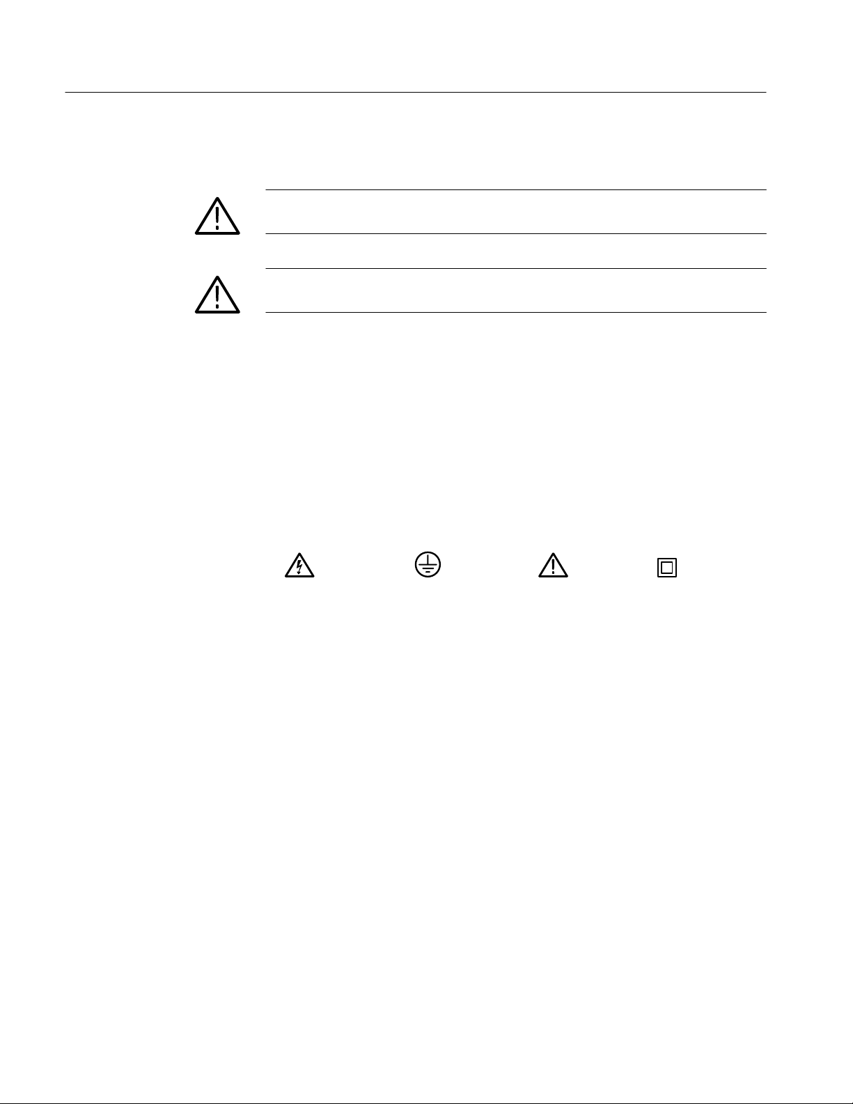
Symbols on the Product. The following symbols may appear on the product:
WARNING
High Voltage
Protective Ground
(Earth) T erminal
CAUTION
Refer to Manual
Double
Insulated
iv
TMS 241 68HC12 Microcontroller Support Instruction Manual
Page 9

Service Safety Summary
Only qualified personnel should perform service procedures. Read this Service
Safety Summary and the General Safety Summary before performing any service
procedures.
Do Not Service Alone. Do not perform internal service or adjustments of this
product unless another person capable of rendering first aid and resuscitation is
present.
Disconnect Power. To avoid electric shock, disconnect the main power by means
of the power cord or, if provided, the power switch.
Use Care When Servicing With Power On. Dangerous voltages or currents may
exist in this product. Disconnect power, remove battery (if applicable), and
disconnect test leads before removing protective panels, soldering, or replacing
components.
To avoid electric shock, do not touch exposed connections.
TMS 241 68HC12 Microcontroller Support Instruction Manual
v
Page 10

Service Safety Summary
vi
TMS 241 68HC12 Microcontroller Support Instruction Manual
Page 11

Preface
This instruction manual contains specific information about the TMS 241
68HC12 microcontroller support package and is part of a set of information on
how to operate this product on compatible Tektronix logic analyzers.
If you are familiar with operating microcontroller support packages on the logic
analyzer for which the TMS 241 68HC12 support was purchased, you will
probably only need this instruction manual to set up and run the support.
If you are not familiar with operating microcontroller support packages, you will
need to supplement this instruction manual with information on basic operations
to set up and run the support.
Information on basic operations of microcontroller support packages is included
with each product. Each logic analyzer has basic information that describes how
to perform tasks common to support packages on that platform. This information
can be in the form of online help, an installation manual, or a user manual.
This manual provides detailed information on the following topics:
H Connecting the logic analyzer to the system under test
Manual Conventions
H Setting up the logic analyzer to acquire data from the system under test
H Acquiring and viewing disassembled data
This manual uses the following conventions:
The term “disassembler” refers to the software that disassembles bus cycles
into instruction mnemonics and cycle types.
The phrase “information on basic operations” refers to online help, an
installation manual, or a basic operations of microcontroller supports user
manual.
In the information on basic operations, the term “XXX” or “P54C” used in
field selections and file names must be replaced with 68HC12. This is the
name of the microcontroller in field selections and file names you must use
to operate the 68HC12 support.
The term “SUT” (system under test) refers to the microcontroller-based
system from which data will be acquired.
TMS 241 68HC12 Microcontroller Support Instruction Manual
vii
Page 12

Preface
The term “logic analyzer” refers to the Tektronix logic analyzer for which
this product was purchased.
The term “HI module” refers to the module in the higher-numbered slot and
the term “LO module” refers to the module in the lower-numbered slot.
68HC12 refers to all supported variations of the 68HC12 microcontroller,
including the 68HC812 and 68HC912 unless otherwise noted.
A tilde (~) following a signal name indicates that the signal is active low.
Logic Analyzer Documentation
A description of other documentation available for each type of Tektronix logic
analyzer is located in the corresponding module user manual. The manual set
provides the information necessary to install, operate, maintain, and service the
logic analyzer and associated products.
Contacting Tektronix
Product
Support
Service
Support
For other
information
To write us
For questions about using Tektronix measurement products, call
toll free in North America:
1-800-TEK-WIDE (1-800-835-9433 ext. 2400)
6:00 a.m. – 5:00 p.m. Pacific time
Or contact us by e-mail:
tm_app_supp@tek.com
For product support outside of North America, contact your
local Tektronix distributor or sales office.
Tektronix offers extended warranty and calibration programs as
options on many products. Contact your local Tektronix
distributor or sales office.
For a listing of worldwide service centers, visit our web site.
In North America:
1-800-TEK-WIDE (1-800-835-9433)
An operator will direct your call.
Tektronix, Inc.
P.O. Box 1000
Wilsonville, OR 97070-1000
USA
viii
Website
Tektronix.com
TMS 241 68HC12 Microcontroller Support Instruction Manual
Page 13

Getting Started
Page 14

Page 15

Getting Started
This chapter contains information on the TMS 241 microcontroller support, and
information on connecting your logic analyzer to your system under test.
Support Package Description
The TMS 241 microcontroller support package displays disassembled data from
systems based on the Motorola 68HC12 family of microcontrollers.
To use this support efficiently, you need to have the items listed in the information on basic operations as well as the following reference material:
68HC12 CPU12 Reference Manual, Motorola, First Edition, 1996,
CPU12RM/AD
MC68HC812A4 Technical Summary: 16-Bit Microcontroller, Motorola,
1997, MC68HC812A4TS/D
Technical Supplement: MC68HC812A4 Electrical Characteristics, Motorola,
16-JAN-97, no part number, this is an online manual
MC68HC912B32 Technical Summary: 16-Bit Microcontroller, Motorola,
1997, MC68HC912B32TS/D
Technical Supplement: MC68HC912B32 Electrical Characteristics,
Motorola, 16-JAN-97, no part number, this is an online manual
Logic Analyzer Software Compatibility
The label on the microcontroller support floppy disk states which version of logic
analyzer software this support is compatible with.
Logic Analyzer Configuration
For use with a TLA 700 Series, the TMS 241 support requires a minimum of
one 102-channel module.
For use with a DAS 9200 Series, the TMS 241 support requires a minimum of
one 96-channel module.
TMS 241 68HC12 Microcontroller Support Instruction Manual
1–1
Page 16

Getting Started
Requirements and Restrictions
Review the Specifications chapter in this manual as they pertain to your system
under test, as well as the following descriptions of other 68HC12 support
requirements and restrictions.
System Clock Rate. The 68HC12 microcontroller support can acquire data from
the 68HC12 microcontroller operating at speeds of up to 8 MHz. This specification is valid at the time this manual was printed. Please contact your Tektronix
Sales Representative for current information on the fastest devices supported.
Custom Clocking. The TMS 241 microcontroller support disassembler requires
Custom clocking in order to function correctly. Other clocking selections like
Internal and External may cause incorrect disassembly.
Hardware Reset. If a hardware reset occurs in your 68HC12 system during an
acquisition, the application disassembler may acquire an invalid sample.
Marking Cycles. The 68HC12 disassembler does not support the marking of
cycles.
Labeling P6434 Probes
The TMS 241 channel assignments follow the standard channel mapping and
labeling scheme for P6434 probes. Apply labels using the standard method as
described in the P6434 Mass Termination Probe Instructions.
DAS Mass Termination Interface (MTIF) Probes
The MTIF probes are already labeled since the probe sections for each probe are
permanent. The TMS 241 channel assignments follow the standard channel
mapping.
Channel Assignments
Channel assignments shown in Table 1–1 through Table 1–7 use the following
conventions:
1–2
H Unless otherwise indicated, all signals are required by the support.
H Channels are shown starting with the most significant bit (MSB) descending
to the least significant bit (LSB).
TMS 241 68HC12 Microcontroller Support Instruction Manual
Page 17

Getting Started
H Channel group assignments are for all modules unless otherwise noted.
H A tilde (~) following a signal name indicates an active low signal.
H The module in the higher-numbered slot is referred to as the HI module and
the module in the lower-numbered slot is referred to as the LO module.
The TLA 704 has the lower numbered slots on the top and the TLA 711 has
the lower numbered slots on the left.
By default the Address group channel assignments are displayed in hexadecimal.
T able 1–1: Address group channel assignments
Bit order Section:channel 68HC12 signal name
15 A1:7 PA7/A15
14 A1:6 PA6/A14
13 A1:5 PA5/A13
12 A1:4 PA4/A12
11 A1:3 PA3/A11
10 A1:2 PA2/A10
9 A1:1 PA1/A9
8 A1:0 PA0/A8
7 A0:7 PB7/A7
6 A0:6 PB6/A6
5 A0:5 PB5/A5
4 A0:4 PB4/A4
3 A0:3 PB3/A3
2 A0:2 PB2/A2
1 A0:1 PB1/A1
0 A0:0 PB0/A0
TMS 241 68HC12 Microcontroller Support Instruction Manual
1–3
Page 18

Getting Started
By default the Data group channel assignments are displayed in hexadecimal.
T able 1–2: Data group channel assignments
Bit order Section:channel 68HC12 signal name
15 D1:7 PC7/D15
14 D1:6 PC6D14
13 D1:5 PC5/D13
12 D1:4 PC4/D12
11 D1:3 PC3/D11
10 D1:2 PC2/D10
9 D1:1 PC1/D9
8 D1:0 PC0/D8
7 D0:7 PD7/D7
6 D0:6 PD6/D6
5 D0:5 PD5/D5
4 D0:4 PD4/D4
3 D0:3 PD3/D3
2 D0:2 PD2/D2
1 D0:1 PD1/D1
0 D0:0 PD0/D0
By default the Control group channel assignments are not visible.
IPIPE1_X and IPIPE0_X refer to the execution information encoded on the
IPIPE signals.
T able 1–3: Control group channel assignments
Bit order Section:channel 68HC12 signal name
4 C2:0 RESET~
3 C0:6 IPIPE1_X
2 C0:2 IPIPE0_X
1 C0:3 PE3/LSTRB~
0 C0:5 PE2/R/W~
1–4
TMS 241 68HC12 Microcontroller Support Instruction Manual
Page 19

Getting Started
By default the Ctrl2 group channel assignments are not visible.
IPIPE1_Q and IPIPE0_Q refer to the queue information encoded on the IPIPE
signals.
Do not probe with the C2:6 and C2:2 channels as they are demuxed from the
C0:6 and C2:2 channels.
T able 1–4: Ctrl2 group channel assignments
Bit order Section:channel 68HC12 signal name
1 C2:6 IPIPE1_Q (demuxed from C0:6)
0 C2:2 IPIPE0_Q (demuxed form C0:2)
By default the Chip_Sel group channel assignments are displayed symbolically.
T able 1–5: Chip_Sel group channel assignments
Bit order Section:channel 68HC12 signal name
6 A3:6
5 A3:5
4 A3:4
3 A3:3
2 A3:2
1 A3:1
0 A3:0
[ Signal not required for disassembly
PF6/CSP1~ [
PF5/CSP0~ [
PF4/CSD~ [
PF3/CS3~ [
PF2/CS2~ [
PF1/CS1~ [
PF0/CS0~ [
By default the Addr_Hi group channel assignments are displayed in hexadecimal.
T able 1–6: Addr_Hi group channel assignments
Bit order Section:channel 68HC12 signal name
5 A2:5
4 A2:4
3 A2:3
2 A2:2
PG5/A21 [
PG4/A20 [
PG3/A19 [
PG2/A18 [
1 A2:1
0 A2:0
[ Signal not required for disassembly.
PG1/A17 [
PG0/A16 [
TMS 241 68HC12 Microcontroller Support Instruction Manual
1–5
Page 20

Getting Started
The probe section and channel assignments for the clock probes are not part of
any group.
T able 1–7: Clock channel assignments
Section:channel 68HC12 signal name
CLK:1 ECLK
CPU To Mictor Connections
To probe the microprocessor you will need to make connections between the
CPU and the Mictor pins of the P6434 Mass Termination Probe. Refer to the
P6434 Mass Termination Probe manual, Tektronix part number 070-9793-xx, for
more information on mechanical specifications. Table 1–8 through Table 1–10
show the CPU pin to Mictor pin connections.
Tektronix uses a counter-clockwise pin assignment. Pin-1 is located at the top
left, and pin-2 is located directly below it. Pin-20 is located on the bottom right,
and pin-21 is located directly above it.
AMP uses an odd side-even side pin assignment. Pin-1 is located at the top left,
and pin-3 is located directly below it. Pin-2 is located on the top right, and pin-4
is located directly below it.
NOTE. When designing Mictor connectors into your SUT, always follow the
Tektronix pin assignment.
Tektronix Pinout AMP Pinout
Pin 1
Pin 19
Pin 38
Pin 20
Pin 1
Pin 37
Pin 2
Pin 38
Figure 1–1: Pin assignments for a Mictor connector (component side)
1–6
TMS 241 68HC12 Microcontroller Support Instruction Manual
Page 21

Getting Started
Please pay close attention to the caution below.
CAUTION. To protect the CPU and the inputs of the module, it is recommended
that a 180W resistor is connected in series between each ball pad of the CPU and
each pin of the Mictor connector. The resistor must be no farther away from the
ball pad of the CPU than 1/2-inch.
T able 1–8: CPU to Mictor connections for Mictor A pins
Tektronix
Mictor A
pin number
1 1 NC NC NC
2 3 NC NC NC
3 5 CLOCK:0 NC NC NC
4 7 A3:7 Not Used Not Used Not Used
5 9 A3:6 PF6/CSP1~ 74 –
6 11 A3:5 PF5/CSP0~ 73 –
7 13 A3:4 PF4/CSD~ 72 –
8 15 A3:3 PF3/CS3~ 71 –
9 17 A3:2 PF2/CS2~ 70 –
10 19 A3:1 PF1/CS1~ 69 –
11 21 A3:0 PF0/CS0~ 68 –
12 23 A2:7 Not Used Not Used Not Used
13 25 A2:6 Not Used Not Used Not Used
14 27 A2:5 PG5/A21 18 –
15 29 A2:4 PG4/A20 17 –
16 31 A2:3 PG3/A19 16 –
17 33 A2:2 PG2/A18 13 –
18 35 A2:1 PG1/A17 12 –
19 37 A2:0 PG0/A16 11 –
20 38 A0:0 PB0/A0 52 18
21 36 A0:1 PB1/A1 53 19
22 34 A0:2 PB2/A2 54 20
23 32 A0:3 PB3/A3 55 21
24 30 A0:4 PB4/A4 56 22
25 28 A0:5 PB5/A5 57 23
26 26 A0:6 PB6/A6 58 24
27 24 A0:7 PB7/A7 59 25
28 22 A1:0 PA0/A8 60 39
AMP
Mictor A
pin number
LA channel 68HC12 signal name
68HC812
pin number
68HC912
pin number
TMS 241 68HC12 Microcontroller Support Instruction Manual
1–7
Page 22

Getting Started
T able 1–8: CPU to Mictor connections for Mictor A pins (cont.)
Tektronix
Mictor A
pin number
29 20 A1:1 PA1/A9 61 40
30 18 A1:2 PA2/A10 62 41
31 16 A1:3 PA3/A11 63 42
32 14 A1:4 PA4/A12 64 43
33 12 A1:5 PA5/A13 65 44
34 10 A1:6 PA6/A14 66 45
35 8 A1:7 PA7/A15 67 46
36 6 CLOCK:1 ECLK 48 29
37 4 NC NC NC NC
38 2 NC NC NC NC
39 39 GND GND GND GND
40 40 GND GND GND GND
41 41 GND GND GND GND
42 42 GND GND GND GND
43 43 GND GND GND GND
AMP
Mictor A
pin number
68HC812
pin num-
68HC12 signal nameLA channel
ber
68HC912
pin number
T able 1–9: CPU to Mictor connections for Mictor C pins
Tektronx
Mictor C
pin number
1 1
2 3
3 5 CLOCK:3
4 7 C3:7
5 9 C3:6 Reserved
6 11 C3:5
7 13 C3:4
8 15 C3:3
9 17 C3:2 Reserved
10 19 C3:1
11 21 C3:0
12 23 C2:7
13 25 C2:6 IPIPE1_Q
14 27 C2:5
AMP
Mictor C
pin number
LA channel 68HC12 signal name
68HC812
pin number
w w
68HC912
pin number
1–8
TMS 241 68HC12 Microcontroller Support Instruction Manual
Page 23

T able 1–9: CPU to Mictor connections for Mictor C pins (cont.)
Getting Started
Tektronx
Mictor C
pin number
15 29 C2:4
16 31 C2:3 PE3/LSTRB~
17 33 C2:2 IPIPE0_Q 49 28
18 35 C2:1
19 37 C2:0 RESET~ 40 32
20 38 C0:0
21 36 C0:1
22 34 C0:2 IPIPE0_X 49 28
23 32 C0:3 PE3/LSTRB2 39 35
24 30 C0:4
25 28 C0:5 PE2/R/W~ 38 36
26 26 C0:6 IPIPE1_X 50 27
27 24 C0:7
28 22 C1:0
29 20 C1:1
30 18 C1:2 Reserved
31 16 C1:3
32 14 C1:4
33 12 C1:5
34 10 C1:6 Reserved
35 8 C1:7
36 6 NC
37 4 NC
38 2 NC
39 39 GND
40 40 GND
41 41 GND
42 42 GND
43 43 GND
w Do not probe this signal. This signal is demultiplexed internally by the AMS program.
AMP
Mictor C
pin number
68HC812
pin num-
68HC12 signal nameLA channel
ber
w w
68HC912
pin number
TMS 241 68HC12 Microcontroller Support Instruction Manual
1–9
Page 24

Getting Started
NOTE. When the microcontroller is in Byte mode, the data on the lower half of
the data bus, Port D, will be suppressed. If you want to acquire data on Port D
(the lower 8-bits of the data port) while operating in the 8-bit bus mode, you will
have to probe those pins separately by using some unused channels.
T able 1–10: CPU to Mictor connections for Mictor D pins
Tektronix
Mictor D
pin number
1 1
2 3
3 5
4 7 D3:7
5 9 D3:6
6 11 D3:5
7 13 D3:4
8 15 D3:3
9 17 D3:2
10 19 D3:1
11 21 D3:0
12 23 D2:7
13 25 D2:6
14 27 D2:5
15 29 D2:4
16 31 D2:3
17 33 D2:2
18 35 D2:1
19 37 D2:0
20 38 D0:0 PD0/D0 20 18
21 36 D0:1 PD1/D1 21 19
22 34 D0:2 PD2/D2 22 20
23 32 D0:3 PD3/D3 23 21
24 30 D0:4 PD4/D4 24 22
25 28 D0:5 PD5/D5 25 23
26 26 D0:6 PD6/D6 26 24
27 24 D0:7 PD7/D7 27 25
28 22 D1:0 PC0/D8 28 39
29 20 D1:1 PC1/D9 29 40
30 18 D1:2 PC2/D10 30 41
AMP
Mictor D
pin number
LA channel 68HC12 signal name
68HC812
pin number
68HC912
pin number
1–10
TMS 241 68HC12 Microcontroller Support Instruction Manual
Page 25

T able 1–10: CPU to Mictor connections for Mictor D pins (cont.)
Getting Started
Tektronix
Mictor D
pin number
31 16 D1:3 PC3/D1 1 31 42
32 14 D1:4 PC4/D12 32 43
33 12 D1:5 PC5/D13 33 44
34 10 D1:6 PC6/D14 34 45
35 8 D1:7 PC7/D15 35 46
36 6 CLOCK:2
37 4 NC NC NC NC
38 2 NC NC NC NC
39 39 GND GND GND GND
40 40 GND GND GND GND
41 41 GND GND GND GND
42 42 GND GND GND GND
43 43 GND GND GND GND
AMP
Mictor D
pin number
68HC812
pin num-
68HC12 signal nameLA channel
ber
68HC912
pin number
TMS 241 68HC12 Microcontroller Support Instruction Manual
1–11
Page 26

Getting Started
1–12
TMS 241 68HC12 Microcontroller Support Instruction Manual
Page 27

Operating Basics
Page 28

Page 29

Setting Up the Support
Information in this section is specific to the operations and functions of the
TMS 241 68HC12 support on any Tektronix logic analyzer for which it can be
purchased. Information on basic operations describes general tasks and functions.
Before you acquire and display disassembled data, you need to load the support
and specify setups for clocking and triggering as described in the information on
basic operations. The support provides default values for each of these setups,
but you can change them as needed.
Channel Group Definitions
The software automatically defines channel groups for the support. If you want to
know which signal is in which group, refer to the channel assignment tables
beginning on page 1–2.
Show Cycles
Clocking
Custom Clocking
Clocking Options
Timing Considerations
A Show cycle is defined as any internal bus cycle made visible on the external
bus. These types of cycles are acquired when you select Included.
A special clocking program is loaded to the module every time you load the
68HC12 support. This special clocking is called Custom.
With Custom clocking, the module logs in signals from multiple groups of
channels at different times as they become valid on the 68HC12 bus. The module
then sends all the logged-in signals to the trigger machine and to the memory of
the module for storage.
The only clocking option available is 68HC12.
The data is clocked on both the rising and falling edge of the signal ECLK. The
three stages for latching a complete data item follow:
1. The IPIPE Queue Movement information is clocked as the last stage of the
previous data item. Simultaneously as the first part of the cycle information
was latched, the address is latched and held on the rising edge of the clock.
2. The data and the other control signals are clocked in on the falling edge of
the clock.
TMS 241 68HC12 Microcontroller Support Instruction Manual
2–1
Page 30

Setting Up the Support
3. The last part of the cycle stores the IPIPE Execution information. The IPIPE
Execution information is stored on the rising edge of the previous data item
(that was already latched).
The next data cycle starts by latching the address for the next data item.
For a given data item the address is latched first, then the data, control, and IPIPE
Execution information, and finally the IPIPE Queue movement.
In analyzing the data, the IPIPE_X (IPIPE Execution) information is to be
applied before the IPIPE_Q (IPIPE Queue) information.
CLK
ADDR (15:0)
DATA (15:0)
READ
DATA (15:0)
WRITE
R/W
LSTRB
CS
IPIPE
IPIPE_Q
Figure 2–1: 68HC12 bus timing
IPIPE_X
IPIPE_Q
2–2
TMS 241 68HC12 Microcontroller Support Instruction Manual
Page 31

Symbols
Setting Up the Support
The TMS 241 support supplies three symbol table files. The 68HC12_CS symbol
file may be used for triggering or display. The 68HC12Ctl2 symbol file may be
used for triggering or display. The 68HC12Ctrl symbol file may be used for
triggering or display.
Table 2–1 lists the name, bit pattern, and description for the symbols in the file
68HC12_CS, the Chip_Sel channel group symbol table.
T able 2–1: Chip_Sel group symbol table definitions
Chip_Sel group value
PF6/CSP1~ PF2/CS2~
Symbol
CSP1~ 011 1111 Chip select program space 1
CSP0~ 101 1111 Chip select program space 0
CSD~ 110 1111 Chip select data space
CS3~ 111 0111 Chip select 3
CS2~ 111 1011 Chip select 2
CS1~ 111 1101 Chip select 1
CS0~ 111 1110 Chip select 0
PF5/CSP0~ PF1/CS1~
PF4/CSD~ PF0/CS0~
PF3/CS3~
Description
Table 2–2 lists the name, bit pattern, and description for the symbols in the
68HC12Ctl2 channel group symbol table.
T able 2–2: Ctrl2 group symbol table definitions
Ctrl2 group value
Symbol
NoQueueMv 00 No queue movement
LtchBus 01 Latch the previous data to the buffer
AdvLdBus 10 Advance the queue and load from the
AdvLdLtch 11 Advance the queue and load from the
IPIPE1_Q
IPIPE0_Q
Description
bus
latch
TMS 241 68HC12 Microcontroller Support Instruction Manual
2–3
Page 32

Setting Up the Support
Table 2–3 lists the name, bit pattern, and description for the symbols in the
68HC12Ctrl channel group symbol table.
T able 2–3: Control group symbol table definitions
Control group value
RESET~
PE6/IPIPE1
PE5/IPIPE0
Symbol
RESET~ 0XXXX RESET
NoStart 100XX No start execution
StrtInt 101XX Start the interrupt sequence
StrtEven 110XX Start execution with the even byte
StrtOdd 111XX Start execution with the odd byte
LSTRB~ 1XX0X Low byte strobe
WORD READ 1 XXX1 Read cycle
WORD WRITE 1XXX0 Write cycle
PE3/LSTRB~
PE2/R/W~
Description
2–4
TMS 241 68HC12 Microcontroller Support Instruction Manual
Page 33

Acquiring and Viewing Disassembled Data
Acquiring Data
Once you load the 68HC12 support and specify the trigger, you are ready to
acquire and disassemble data.
If you have any problems acquiring data, refer to information on basic operations
in your online help or Appendix A: Error Messages and Disassembly Pr oblems in
the basic operations user manual.
Viewing Disassembled Data
You can view disassembled data in four display formats: Hardware, Software,
Control Flow, and Subroutine. The information on basic operations describes
how to select the disassembly display formats.
NOTE. Selections in the Disassembly property page (the Disassembly Format
Definition overlay) must be set correctly for your acquired data to be disassembled correctly. Refer to Changing How Data is Displayed on page 2–8.
The default display format shows the Address, Data, and Control channel group
values for each sample of acquired data.
If a channel group is not visible, you must use the Disassembly property page to
make the group visible.
The disassembler displays special characters and strings in the instruction
mnemonics to indicate significant events. Table 2–4 lists these special characters
and strings, and gives a definition of what they represent.
T able 2–4: Description of special characters in the display
Character or string displayed Description
>> on the TLA 700
m on the DAS 9200
**** Indicates there is insufficient data available for complete
# Indicates an immediate value
t Indicates the number shown is in decimal, such as #12t
The interpretation of the instruction was manually changed
using the Mark Cycle function
disassembly of the instruction. The number of asterisks
indicates the width of the data that is unavailable. Each two
asterisks represent one byte.
TMS 241 68HC12 Microcontroller Support Instruction Manual
2–5
Page 34

Acquiring and Viewing Disassembled Data
Hardware Display Format
In Hardware display format, the disassembler displays certain cycle type labels in
parentheses. Reads to interrupt and exception vectors will be labeled with the
vector name. The following is a list of cycle type labels.
( BYTE READ )
( BYTE WRITE )
( WORD READ )
( WORD WRITE )
( RESET )
( INTURRUPT SEQUENCE )
( INTERNAL )
( FLUSH )
( EXTENSION )
Displaying Exception
2–6
Vectors
Figure 2–2: Example of the hardware display
When a vector read caused by an execution is detected, it will be labeled with the
vector name. The following are the Interrupt/Exception labels:
( VECTOR:SYSTEM RESET )
( VECTOR:COP RESET )
( VECTOR:IRQ )
( VECTOR:TIMER CHANNEL 0 )
( VECTOR:TIMER CHANNEL 1 )
( VECTOR:TIMER CHANNEL 2 )
( VECTOR:TIMER CHANNEL 3 )
( VECTOR:TIMER CHANNEL 4 )
( VECTOR:TIMER CHANNEL 5 )
( VECTOR:TIMER CHANNEL 6 )
TMS 241 68HC12 Microcontroller Support Instruction Manual
Page 35

Acquiring and Viewing Disassembled Data
( VECTOR:TIMER CHANNEL 7 )
( VECTOR:TIMER OVERFLOW )
( VECTOR: PULSE ACC OVERFLOW )
( VECTOR: PULSE ACC INP EDGE )
( VECTOR:SCI 0 )
( VECTOR:SCI 1 )
( VECTOR:ATD )
( VECTOR:KEY WAKEUP J )
( VECTOR:KEY WAKEUP H )
( VECTOR:RESERVED )
Software Display Format
Control Flow Display
Format
The Software display format shows only the first fetch of executed instructions.
Flushed cycles and extensions are not shown, even though they are part of the
executed instruction. Read extensions will be used to disassemble the instruction,
but will not be displayed as a separate cycle in the Software display format. Data
reads and writes are not displayed.
In the Control Flow display format, only the first fetch of instructions that change
the flow of control, or cause a branch in the addressing will be displayed.
If a conditional branch branches to an address that is reached sequentially, it
might be impossible to determine if the branch was taken. If this happens the
branch will not be displayed in the Control Flow display, and no flushing will be
done by the software. Unconditional branches are always displayed whether or
not the destination address is seen on the bus.
Instructions that unconditionally generate a change in the flow of control in the
68HC12 microcontroller are as follows:
BRA LBRA BSR CALL JMP
JSR RTC RTS WAI RTI
SWI TRAP
Instructions that conditionally generate a change in the flow of control in the
68HC12 microcontroller are as follows:
BCC BCS BEQ BGND BMI
BNE BPL BVC BVS BHI
BHS BLO BLS BGE BGT
BLE BLT BRCLR BRSET LBCC
LBCS LBEQ LBMI LBNE LBPL
LBVC LBVS LBHI LBHS LBLO
LBLS LBGE LBGT LBLE LBLT
DBEQ DBNE IBEQ IBNE STOP
TBEQ TBNE
TMS 241 68HC12 Microcontroller Support Instruction Manual
2–7
Page 36

Acquiring and Viewing Disassembled Data
Subroutine Display
Format
The Subroutine display format shows only the first fetch of subroutine call and
return instructions. It will display conditional subroutine calls if they are
considered to be taken.
Instructions that unconditionally generate a subroutine call or a return in the
68HC12 microcontroller are as follows:
BSR CALL JMP JSR
RTC RTS WAI RTI
SWI TRAP
Instructions that conditionally generate a subroutine call or a return in the
68HC12 microcontroller are as follows:
There are no conditional subroutine calls.
Changing How Data is Displayed
There are common fields and features that allow you to further modify displayed
data to suit your needs. You can make common and optional display selections in
the Disassembly property page (the Disassembly Format Definition overlay).
You can make selections unique to the 68HC12 support to do the following tasks.
Optional Display
Selections For the
TLA 700
You can make optional selections for acquired disassembled data. In addition to
the common selections that is described in the information on basic operations,
you can change the displayed data in the following ways:
Show: Hardware (default setting)
Software
Control Flow
Subroutine
Highlight: Software (default setting)
Control Flow
Subroutine
None
Disassemble Across Gaps: Yes (default setting)
No
2–8
TMS 241 68HC12 Microcontroller Support Instruction Manual
Page 37

Acquiring and Viewing Disassembled Data
Optional Display
Selections For the
DAS 9200
You can make optional selections for acquired disassembled data. In addition to
the common selections that is described in the information on basic operations,
you can change the displayed data in the following ways:
Display Mode: Hardware (default setting)
Software
Control Flow
Subroutine
Timestamp: Relative (default setting)
Delta
Absolute
Off
Highlight: All
Instructions (default setting)
Control Flow
Subroutines
Highlight gaps: Yes (default setting)
No
Optional Display
Selections
Marking Cycles
Disasm Across Gaps: Yes
No (default setting)
The TMS 241 will add a field to the Define Format overlay (F5) to allow you to
select between a 16- and 8-bit bus. The field name is Bus Width.
The disassembler needs this information to know where to find the data for
correct disassembly. You must select either Byte Mode or Word Mode. The the
default selection is Word Mode.
The TMS 241
read extensions and flush cycles). If the cursor is placed on any other cycle type,
no cycle marks will be available.
TLA 700 Series. Marks are placed by using the Mark Opcode button. The Mark
Opcode button is always be available. If the sample being marked is not an
instruction fetch cycle, the Mark Opcode selections will be replaced by a note
indicating that “An Opcode Mark cannot be placed at the selected data sample.”
will only allow marking of instruction fetch cycles (which include
TMS 241 68HC12 Microcontroller Support Instruction Manual
2–9
Page 38

Acquiring and Viewing Disassembled Data
When a cycle is marked, the character “>>” is displayed immediately to the left
of the Mnemonics column. Cycles can be unmarked by using the “Undo Mark”
selection, which will remove the character “>>”.
DAS 9200 Series. Marks are placed by using the F4 key: Mark Data function key.
The Mark Data function key is always be available. If the cursor is not on an
instruction fetch cycle, then no microprocessor cycle marks will be available
when the key is pressed.
When a cycle is marked, the letter “m” is displayed immediately to the left of the
Sequence column. Cycles can be unmarked by using the “Undo Mark” selection,
which will remove the letter “m”.
Cycle Marking
The TMS 241 supports cycle marks. In Byte Mode the following marks are
available:
Opcode
Extension
Flush
Data
Internal
Undo Mark
In Word Mode the following marks are available:
Even/Odd Opcode/Opcode
Even/Odd Opcode/Extension
Even/Odd Extension/Opcode
Even/Odd Extension/Extension
Even/Odd Flush/Opcode
Even/Odd Opcode/Flush
Even/Odd Extension/Flush
Even/Odd Flush/Flush
Even/Odd Data
Even/Odd Internal
Undo Mark
Microprocessor Specific Disassembly Restrictions
The 68HC12 can function as a single chip microcomputer with all of the pins set
up as I/O to control hardware. When the 68HC12 is operating in this mode the
TMS 241 software cannot acquire program execution correctly. In order for the
TMS 241 software to acquire useful disassembly, the 68HC12 must be configured so that the support can acquire bus activity.
2–10
TMS 241 68HC12 Microcontroller Support Instruction Manual
Page 39

Acquiring and Viewing Disassembled Data
In order for the TMS 241 to successfully acquire data the 68HC12 must be
configured so that the acquisition software has access to the following:
H ECLK (PE4) must be configured to stretch instead of free running in the
Mode Register.
H The 16-bits of the address: Port A and Port B
H The data: either as an 8- or 16-bit data bus depending on the configuration;
Port C and Port D
H The Pipe Status signals (PE[6-5])
The following signals are used, and have a small effect on the disassembler:
H The R/W signal (PE2) that distinguishes the read cycles from the write cycles
H LSTRB (PE3) is used to distinguish the byte and word cycles; and which
byte is valid.
H The mode register can be set to allow internal cycles from the internal
EEPROM and RAM to be visible on the external bus, which can also be
controlled by the mode select signals at reset time.
H The reset line is monitored and used in the clocking algorithm of the support.
The TMS 241 can provide support for:
H Either an 8- or 16-bit bus. The system bus width can be selected in the
disassembly properties window, and defaults to a 16-bit bus.
H High address bits A16 through A21, Port G
H Symbolic support for the chip select bits, Port F
Figure 2–3 shows a sample acquisition after power up reset. After power up
reset, and until the ports are initialized, the Pipe Status signals are not set
correctly and therefore disassembly is not reliable.
In Figure 2–3 the Data group is indicated to be in byte mode. The raw data group
is not normally enabled, but it can be when you want to know what is on the
entire bus when the control signals are correct.
You can use the Mark Opcode feature to force the disassembler to show
mnemonics. In Figure 2–3 Sequence numbers 9 through 13 have been marked,
and have the marking symbol >> preceding the mnemonic, and force the
( Byte Read ) to show the mnemonic.
TMS 241 68HC12 Microcontroller Support Instruction Manual
2–11
Page 40

Acquiring and Viewing Disassembled Data
Figure 2–3: Sample disassembly after a power up reset
2–12
TMS 241 68HC12 Microcontroller Support Instruction Manual
Page 41

Specifications
Page 42

Page 43

Specifications
Specification Tables
This chapter containes information regarding the specifications of the support.
Table 3–1 lists specifications the system under test must produce for the support
to correctly acquire data.
T able 3–1: Specifications
Characteristics Requirements
system under test clock rate
Clock rate Maximum 8 MHz
Minimum setup time required
TLA 700 2.5 ns
DAS 9200 5 ns
Minimum hold time required
TLA 700 0 ns
DAS 9200 0 ns
TMS 241 68HC12 Microcontroller Support Instruction Manual
3–1
Page 44

Specifications
3–2
TMS 241 68HC12 Microcontroller Support Instruction Manual
Page 45

Replaceable Parts
Page 46

Page 47

Replaceable Parts
This section contains a list of the replaceable parts for the TMS 241 68HC12
microcontroller support product.
Parts Ordering Information
Replacement parts are available through your local Tektronix field office or
representative.
Changes to Tektronix products are sometimes made to accommodate improved
components as they become available and to give you the benefit of the latest
improvements. Therefore, when ordering parts, it is important to include the
following information in your order.
H Part number
H Instrument type or model number
H Instrument serial number
H Instrument modification number, if applicable
Abbreviations
Mfr. Code to Manufacturer
Cross Index
If you order a part that has been replaced with a different or improved part, your
local Tektronix field office or representative will contact you concerning any
change in part number.
Abbreviations conform to American National Standard ANSI Y1.1–1972.
The table titled Manufacturers Cross Index shows codes, names, and addresses
of manufacturers or vendors of components listed in the parts list.
TMS 241 68HC12 Microcontroller Support Instruction Manual
4–1
Page 48

Replaceable Parts
Manufacturers cross index
Mfr.
code
80009 TEKTRONIX INC 14150 SW KARL BRAUN DR
Manufacturer Address City , state, zip code
PO BOX 500
Replaceable parts list
Fig. &
index
number
Tektronix
part number
071–0145–00 1 MANUAL, TECH: INSTRUCTIONS, 68HC12, TMS241, 80009 071–0145–00
070–9803–00 1 MANUAL, TECH: INSTRUTION, MICROPROCESSOR
070–9802–00 1 MANUAL, TECH: BASIC OPS MICRO SUP ON
Serial no.
effective
Serial no.
discont’d
Qty Name & description Mfr. code Mfr. part number
SUPPORT, PKG INSTALLATION, TLA700 SERIES,
LOGIC ANALYZER
OPTIONAL ACCESSORIES
DAS/TLA 500 SERIES LOGIC ANALYZERS
BEAVERT ON, OR 97077–0001
80009 070–9803–00
80009 070–9802–00
4–2
TMS 241 68HC12 Microcontroller Support Instruction Manual
Page 49

Index
Page 50

Page 51

Index
A
about this manual set, vii
acquiring data, 2–5
Address group, channel assignments, 1–3
application, logic analyzer configuration, 1–1
B
basic operations, where to find information, vii
bus cycles, displayed cycle types, 2–6
C
channel assignments
Address group, 1–3
Chip_Sel, 1–5
clocks, 1–6
Control group, 1–4
Ctrl2, 1–5
Data group, 1–4
Misc group, 1–5
channel group definitions, 2–1
channel groups, visibility, 2–5
Chip_Sel, channel assignments, 1–5
Chip_Sel group, symbol table, 2–3
clock channel assignments, 1–6
clock rate, 1–2
maximum, 3–1
clocking
clocking options, 2–1
custom clocking, 2–1
timing considerations, 2–1
clocking options, 2–1
Show Cycles, 2–1
connections, CPU to Mictor, 1–6
contacting T ektronix, viii
Control Flow display format, 2–7
Control group
channel assignments, 1–4
symbol table, 2–4
CPU to Mictor connections, 1–6
Ctrl2, channel assignments, 1–5
Ctrl2 group, symbol table, 2–3
Custom clocking, Show Cycles, 2–1
custom clocking, restrictions, 1–2
cycle types, 2–6
D
data
acquiring, 2–5
disassembly formats
Control Flow, 2–7
Software, 2–7
subroutine, 2–8
data display , changing, 2–8
Data group, channel assignments, 1–4
definitions
disassembler, vii
HI module, viii
information on basic operations, vii
LO module, viii
logic analyzer, viii
P54C, vii
SUT, vii
XXX, vii
disassembled data
cycle type definitions, 2–6
viewing, 2–5
disassembler
definition, vii
logic analyzer configuration, 1–1
setup, 2–1
Disassembly Format Definition overlay, 2–8, 2–9
Disassembly property page, 2–8, 2–9
display formats
Control Flow, 2–7
Software, 2–7
special characters, 2–5
subroutine, 2–8
E
exception vectors, 2–6
F
flow of control
conditional, 2–7
unconditional, 2–7
TMS 241 68HC12 Microcontroller Support Instruction Manual
Index–1
Page 52

Index
H
Hardware display format, cycle type definitions, 2–6
HI module, definition, viii
hold time, minimum, 3–1
I
IPIPE Execution information, 2–2
IPIPE Queue Movement information, 2–1
IPIPE_Q, 2–2
IPIPE_X, 2–2
L
LO module, definition, viii
logic analyzer
configuration for disassembler, 1–1
configuration for the application, 1–1
with a DAS 9200 series, 1–1
with a TLA 700 series, 1–1
definition, viii
software compatibility, 1–1
M
manual
conventions, vii
how to use the set, vii
manufacturers cross reference, 4–2
Mark Cycle function, 1–2
Mark Opcode function, 1–2
marking cycles, 2–9
unavailable, 1–2
Mictor to CPU connections, 1–6
Misc group, channel assignments, 1–5
MTIF probes, 1–2
Reset, SUT hardware, 1–2
restrictions, 1–2
clock rate, 1–2
custom clocking, 1–2
S
setup time, minimum, 3–1
setups
disassembler, 2–1
support, 2–1
Show Cycles, clocking option, 2–1
signals, active low sign, viii
Software display format, 2–7
special characters displayed, 2–5
specification tables, 3–1
specifications, 3–1
channel assignments, 1–2
subroutine display format, 2–8
support, setup, 2–1
support setup, 2–1
SUT, definition, vii
SUT hardware Reset, 1–2
symbol table
Chip_Sel channel group, 2–3
Control channel group, 2–4
Ctrl2 channel group, 2–3
system clock rate, 1–2
T
T ektronix, how to contact, viii
terminology, vii
timing considerations, 2–1
V
viewing disassembled data, 2–5
P
P54C, definition, vii
P6434 probes, labeling, 1–2
parts ordering information, 4–1
R
replaceable parts list, 4–2
Index–2
X
XXX, definition, vii
TMS 241 68HC12 Microcontroller Support Instruction Manual
 Loading...