

Page 1

Instruction Manual
TMS230
MMC2107 Microcontroller Software Support
071-0894-00
www.tektronix.com
Page 2

Copyright © T ektronix, Inc. All rights reserved. Licensed software products are owned by Tektronix or its suppliers and
are protected by United States copyright laws and international treaty provisions.
Use, duplication, or disclosure by the Government is subject to restrictions as set forth in subparagraph (c)(1)(ii) of the
Rights in T echnical Data and Computer Software clause at DFARS 252.227-7013, or subparagraphs (c)(1) and (2) of the
Commercial Computer Software – Restricted Rights clause at F AR 52.227-19, as applicable.
T ektronix products are covered by U.S. and foreign patents, issued and pending. Information in this publication supercedes
that in all previously published material. Specifications and price change privileges reserved.
T ektronix, Inc., P.O. Box 500, Beaverton, OR 97077
TEKTRONIX and TEK are registered trademarks of T ektronix, Inc.
Page 3

SOFTWARE WARRANTY
T ektronix warrants that the media on which this software product is furnished and the encoding of the programs on
the media will be free from defects in materials and workmanship for a period of three (3) months from the date of
shipment. If a medium or encoding proves defective during the warranty period, T ektronix will provide a
replacement in exchange for the defective medium. Except as to the media on which this software product is
furnished, this software product is provided “as is” without warranty of any kind, either express or implied.
T ektronix does not warrant that the functions contained in this software product will meet Customer’s
requirements or that the operation of the programs will be uninterrupted or error-free.
In order to obtain service under this warranty, Customer must notify Tektronix of the defect before the expiration
of the warranty period. If T ektronix is unable to provide a replacement that is free from defects in materials and
workmanship within a reasonable time thereafter, Customer may terminate the license for this software product
and return this software product and any associated materials for credit or refund.
THIS WARRANTY IS GIVEN BY TEKTRONIX IN LIEU OF ANY OTHER WARRANTIES, EXPRESS
OR IMPLIED. TEKTRONIX AND ITS VENDORS DISCLAIM ANY IMPLIED WARRANTIES OF
MERCHANTABILITY OR FITNESS FOR A P ARTICULAR PURPOSE. TEKTRONIX
RESPONSIBILITY TO REPLACE DEFECTIVE MEDIA OR REFUND CUSTOMER’S PAYMENT IS
THE SOLE AND EXCLUSIVE REMEDY PROVIDED TO THE CUSTOMER FOR BREACH OF THIS
WARRANTY. TEKTRONIX AND ITS VENDORS WILL NOT BE LIABLE FOR ANY INDIRECT,
SPECIAL, INCIDENTAL, OR CONSEQUENTIAL DAMAGES IRRESPECTIVE OF WHETHER
TEKTRONIX OR THE VENDOR HAS ADVANCE NOTICE OF THE POSSIBILITY OF SUCH
DAMAGES.
Page 4

Page 5

Table of Contents
Getting Started
Operating Basics
Preface vii. . . . . . . . . . . . . . . . . . . . . . . . . . . . . . . . . . . . . . . . . . . . . . . . . . .
Manual Conventions vii. . . . . . . . . . . . . . . . . . . . . . . . . . . . . . . . . . . . . . . . . . . . . .
Contacting T ektronix viii. . . . . . . . . . . . . . . . . . . . . . . . . . . . . . . . . . . . . . . . . . . . . .
Support Package Description 1–1. . . . . . . . . . . . . . . . . . . . . . . . . . . . . . . . . . . . . . . .
Logic Analyzer Software Compatibility 1–1. . . . . . . . . . . . . . . . . . . . . . . . . . . . . . .
Logic Analyzer Configuration 1–1. . . . . . . . . . . . . . . . . . . . . . . . . . . . . . . . . . . . . . .
Requirements and Restrictions 1–1. . . . . . . . . . . . . . . . . . . . . . . . . . . . . . . . . . . . . . .
Functinality Not Supported 1–2. . . . . . . . . . . . . . . . . . . . . . . . . . . . . . . . . . . . . . . . .
Connecting the Logic Analyzer to a System Under T est 1–2. . . . . . . . . . . . . . . . . . .
Setting Up the Support 2–1. . . . . . . . . . . . . . . . . . . . . . . . . . . . . . . . . . . . . .
Installing the Support Software 2–1. . . . . . . . . . . . . . . . . . . . . . . . . . . . . . . . . . . . . .
Channel Group Definitions 2–1. . . . . . . . . . . . . . . . . . . . . . . . . . . . . . . . . . . . . . . . .
Support Package Setups 2–2. . . . . . . . . . . . . . . . . . . . . . . . . . . . . . . . . . . . . . . . . . . .
Clocking 2–2. . . . . . . . . . . . . . . . . . . . . . . . . . . . . . . . . . . . . . . . . . . . . . . . . . . . . . . .
Custom Clocking 2–2. . . . . . . . . . . . . . . . . . . . . . . . . . . . . . . . . . . . . . . . . . . . . . . . .
Acquiring and Viewing Disassembled Data 2–5. . . . . . . . . . . . . . . . . . . . .
Acquiring Data 2–5. . . . . . . . . . . . . . . . . . . . . . . . . . . . . . . . . . . . . . . . . . . . . . . . . . .
Viewing Disassembled Data 2–5. . . . . . . . . . . . . . . . . . . . . . . . . . . . . . . . . . . . . . . .
Timing Display Format 2–6. . . . . . . . . . . . . . . . . . . . . . . . . . . . . . . . . . . . . . . . .
Hardware Display Format 2–6. . . . . . . . . . . . . . . . . . . . . . . . . . . . . . . . . . . . . . .
Software Display Format 2–7. . . . . . . . . . . . . . . . . . . . . . . . . . . . . . . . . . . . . . .
Control Flow Display Format 2–7. . . . . . . . . . . . . . . . . . . . . . . . . . . . . . . . . . . .
Subroutine Display Format 2–8. . . . . . . . . . . . . . . . . . . . . . . . . . . . . . . . . . . . . .
Changing How Data is Displayed 2–8. . . . . . . . . . . . . . . . . . . . . . . . . . . . . . . . . . . .
Optional Display Selections 2–8. . . . . . . . . . . . . . . . . . . . . . . . . . . . . . . . . . . . .
Micro-Specific Fields 2–9. . . . . . . . . . . . . . . . . . . . . . . . . . . . . . . . . . . . . . . . . .
Marking Cycles 2–9. . . . . . . . . . . . . . . . . . . . . . . . . . . . . . . . . . . . . . . . . . . . . . .
Viewing an Example of Disassembled Data 2–10. . . . . . . . . . . . . . . . . . . . . . . . . . . .
Specifications
Specification T ables 3–1. . . . . . . . . . . . . . . . . . . . . . . . . . . . . . . . . . . . . . . . . . . . . . .
Replaceable Parts
Parts Ordering Information 4–1. . . . . . . . . . . . . . . . . . . . . . . . . . . . . . . . . . . . . . . . .
Using the Replaceable Parts List 4–1. . . . . . . . . . . . . . . . . . . . . . . . . . . . . . . . . . . . .
TMS230 MMC2107 Microcontroller Support
i
Page 6

Table of Contents
Reference
Index
Symbol Table 5–1. . . . . . . . . . . . . . . . . . . . . . . . . . . . . . . . . . . . . . . . . . . . . . . . . . . .
Channel Assignments 5–2. . . . . . . . . . . . . . . . . . . . . . . . . . . . . . . . . . . . . . . . . . . . .
CPU To Mictor Connections 5–9. . . . . . . . . . . . . . . . . . . . . . . . . . . . . . . . . . . . . . . .
ii
TMS230 MMC2107 Microcontroller Support
Page 7

List of Figures
Table of Contents
Figure 2–1: Timing diagram of Sample point and Master
sample point 2–3. . . . . . . . . . . . . . . . . . . . . . . . . . . . . . . . . . . . . . . . . . . .
Figure 2–2: Hardware display format 2–7. . . . . . . . . . . . . . . . . . . . . . . . . .
Figure 5–1: Pin assignments for a Mictor connector
(component side) 5–9. . . . . . . . . . . . . . . . . . . . . . . . . . . . . . . . . . . . . . . .
TMS230 MMC2107 Microcontroller Support
iii
Page 8

Table of Contents
List of Tables
Table 2–1: Description of special characters in the display 2–5. . . . . . . .
Table 2–2: Cycle type labels and definitions 2–6. . . . . . . . . . . . . . . . . . . .
Table 3–1: Electrical specifications 3–1. . . . . . . . . . . . . . . . . . . . . . . . . . . .
Table 5–1: MMC2107 _Ctrl group symbol table definitions 5–1. . . . . . .
Table 5–2: Address channel group assignments 5–3. . . . . . . . . . . . . . . . .
Table 5–3: Data channel group assignments 5–4. . . . . . . . . . . . . . . . . . . .
Table 5–4: Control channel group assignments 5–5. . . . . . . . . . . . . . . . . .
Table 5–5: ChipSelect channel group assignments 5–5. . . . . . . . . . . . . . .
Table 5–6: Proc_Mode channel group assignments 5–5. . . . . . . . . . . . . .
Table 5–7: Misc channel group assignments 5–6. . . . . . . . . . . . . . . . . . . .
Table 5–8: Clock and Qualifier channel assignments 5–6. . . . . . . . . . . . .
Table 5–9: Signals required for clocking and disassembly 5–7. . . . . . . . .
Table 5–10: Signals not required for clocking and disassembly 5–8. . . .
Table 5–11: CPU to Mictor connections for clock and qualifiers 5–10. . .
Table 5–12: CPU to Mictor connections for Mictor A pins 5–10. . . . . . . .
Table 5–13: CPU to Mictor connections for Mictor D pins 5–11. . . . . . . .
Table 5–14: CPU to Mictor connections for Mictor C pins 5–12. . . . . . . .
iv
TMS230 MMC2107 Microcontroller Support
Page 9

Preface
Manual Conventions
This instruction manual contains specific information about the
TMS230 MMC2107 microcontroller support package and is part of a set of
information on how to operate this product on compatible Tektronix logic
analyzers.
If you are familiar with operating microcontroller support packages on the logic
analyzer for which the TMS230 MMC2107 support was purchased, you will only
need this instruction manual to set up and run the support.
If you are not familiar with operating microcontroller support packages, you will
need to supplement this instruction manual with information on basic operations
to set up and run the support. See Manual Conventions below for more information.
This manual uses the following conventions:
H The term “disassembler” refers to the software that disassembles bus cycles
into instruction mnemonics and cycle types.
H The phrase “information on basic operations” refers to your logic analyzer
online help or a user manual covering the basic operations of microcontroller
support.
TMS230 MMC2107 Microcontroller Support
v
Page 10

Preface
Contacting Tektronix
Phone 1-800-833-9200*
Address Tektronix, Inc.
Department or name (if known)
14200 SW Karl Braun Drive
P.O. Box 500
Beaverton, OR 97077
USA
Web site www.tektronix.com
Sales support 1-800-833-9200, select option 1*
Service support 1-800-833-9200, select option 2*
Technical support Email: techsupport@tektronix.com
1-800-833-9200, select option 3*
1-503-627-2400
6:00 a.m. – 5:00 p.m. Pacific time
* This phone number is toll free in North America. After office hours, please leave a
voice mail message.
Outside North America, contact a Tektronix sales office or distributor; see the
Tektronix web site for a list of offices.
vi
TMS230 MMC2107 Microcontroller Support
Page 11

Getting Started
Page 12

Page 13

Getting Started
This section contains information on the TMS230 MMC2107 microcontroller
support package and on connecting your logic analyzer to your system under test.
Support Package Description
The TMS230 MMC2107 microcontroller support package displays disassembled
data from systems based on the Motorola MMC2107 microcontroller.
To use this support efficiently, you need to have the items listed in the information on basic operations and Motorola Inc., 02/29/00 User manual, and Sika
Overview Specification rev 1.2.
Information on basic operations in your logic analyzer online help also contains a
general description of the support.
Logic Analyzer Software Compatibility
The floppy disk label on the microcontroller support states the version of logic
analyzer software with which this support is compatible.
Logic Analyzer Configuration
The TMS230 MMC2107 support requires a minimum of one 102-channel
module.
Requirements and Restrictions
Review the general requirements and restrictions of microcontroller support
packages as they pertain to your system under test.
Also review electrical specifications in Specifications on page 3–1 as they pertain
to your system under test, as well as the following descriptions of other
MMC2107 support requirements and restrictions.
System Clock Rate
The operating speeds with which the MMC2107
the MMC2107 microcontroller are listed on Table 3–1. These specifications were
valid at the time this manual was printed. Contact your Tektronix Sales Representative for current information on the fastest devices supported.
support can acquire data from
TMS230 MMC2107 Microcontroller Support
1–1
Page 14

Getting Started
NonIntrusive Acquisition
Disabling the Instruction
Cache
Acquiring microcontroller bus cycles is nonintrusive to your system under test.
That is, the TMS230 MMC2107 support does not intercept, modify, or present
signals back to your system under test.
The cache is not present on the MMC2107 microcontroller. All instruction
prefetches are visible on the bus so they can be acquired and displayed
disassembled.
Functionality Not Supported
FAST Mode
Single Chip Mode
Fast mode is for factory testing only.
In Single Chip mode all memory is internal to the chip.
Connecting the Logic Analyzer to Your System Under Test
You can use channel probes, clock probes, and leadsets with a commercial test
clip (or adapter) to make connections between the logic analyzer and your system
under test.
To connect the probes to MMC2107 signals in your system under test using a test
clip, follow these steps:
1. Power off your system under test. It is not necessary to power off the logic
analyzer.
CAUTION. To prevent static damage, handle the microcontroller, the probes, and
the logic analyzer module components only in a static-free environment. Static
discharge can damage these components.
Always wear a grounding wrist strap, heel strap, or similar device while
handling the microcontroller.
2. To discharge your stored static electricity, touch the ground connector located
on the back of the logic analyzer. If you are using a test clip, touch any of the
ground pins on the clip to discharge stored static electricity from the test clip.
CAUTION. To prevent damage to the pins on the microcontroller, place your
system under test on a horizontal static-free surface before connecting the test
clip.
1–2
TMS230 MMC2107 Microcontroller Support
Page 15

Getting Started
3. Use Tables 5–2 through 5–10 beginning on page 5–3 to connect the channel
probes to MMC2107 signal pins on the test clip or in your system under test.
Use leadsets to connect at least one ground lead from each channel probe and
the ground lead from each clock probe to ground pins on your test clip.
TMS230 MMC2107 Microcontroller Support
1–3
Page 16

Getting Started
1–4
TMS230 MMC2107 Microcontroller Support
Page 17

Operating Basics
Page 18

Page 19

Setting Up the Support
The information in this section is specific to the operations and functions of the
TMS230 MMC2107 microcontroller support on any Tektronix logic analyzer for
which it can be purchased.
Before you acquire and display disassembled data, you need to load the support
and specify setups for clocking and triggering as described in the information on
basic operations in your logic analyzer online help. The microcontroller support
provides default values for each of these setups as well as user-definable settings.
Installing the Support Software
NOTE. Before you install any software, it is recommended that you verify that the
microcontroller support software is compatible with the logic analyzer software.
To install the TMS230 MMC2107 software on your Tektronix logic analyzer,
follow these steps:
1. Insert the floppy disk in the disk drive.
2. Click the Windows Start button, point to Settings, and click Control Panel.
3. In the Control Panel window, double-click Add/Remove Programs.
4. Follow the instructions on the screen for installing the software from the
To remove or uninstall software, close all windows, and then follow the above
instructions and select Uninstall.
Channel Group Definitions
The software automatically defines channel groups for the support. The channel
groups for the TMS230 MMC2107 support are Address, Data, Control,
Proc_Mode, ChipSelect, and Misc. The channel group tables begin on page 5–1.
floppy disk.
TMS230 MMC2107 Microcontroller Support
2–1
Page 20

Setting Up the Support
Support Package Setups
The TMS230 MMC2107 software installs the MMC2107 support package setup
file.
Clocking
MMC2107 Setup
Options
This setup provides disassembly support. Signals are displayed as they appear
electrically on the front side bus.
The TMS230 MMC2107 support offers a microcontroller-specific clocking mode
for the MMC2107 microcontroller. This clocking mode is the default selection
whenever you load the TMS230 MMC2107 support.
Disassembly is not correct when using the Internal or External clocking modes.
Information on basic operations in your online help describes in more detail how
to use these clock selections for general purpose analysis.
H Internal clocking is used for timing and is based on the clock generated by a
Tektronix logic analyzer. You can configure the clock rate from 50 ms down
to 4 ns resolution.
H External clocking is used when you configure the clocking of data based on
logical combinations of clocks and qualifiers.
Custom Clocking
2–2
When Custom is selected, the Custom Clocking Options menu has the subtitle
MMC2107 microcontroller Clocking Support added, and the clocking option is
displayed.
The TMS230 MMC2107 support has one clocking option:
External Bus Interface
The External Bus interface option supports both Emulation mode and Master
mode. In Emulation mode the SHS~ signal is enabled by default. For Master
mode to function correctly, the SHS~ signal must be enabled.
In Master mode, the SHS~ signal is enabled by writing to the port E pin
assignment register (PEPAR).
TMS230 MMC2107 Microcontroller Support
Page 21

Setting Up the Support
Figure 2–1 shows the bus timing for External Bus Interface (EBI) Memory Read
cycle.
SHS~
R/W~
A[22:0], TSIZ[1:0]
DATA [31:0]
CS~
OE~
EB[3:0]~
TA~, TEA~
A1
Sample Point
for Address, EB,
and Control
A2
D1
Sample Point for
Data and
Master Point
Figure 2–1: Timing diagram of Sample point and Master sample point
TMS230 MMC2107 Microcontroller Support
2–3
Page 22

Setting Up the Support
2–4
TMS230 MMC2107 Microcontroller Support
Page 23

Acquiring and Viewing Disassembled Data
Acquiring Data
After you load the TMS230 MMC2107 support, choose a clocking mode, and
specify the trigger, you are ready to acquire and disassemble data.
If you have any problems acquiring data, refer to information on basic operations
in your logic analyzer online help or Appendix A: Error Messages and
Disassembly Problems in your logic analyzer user manual.
Viewing Disassembled Data
You can view disassembled data in six display formats: Timing, State, Hardware,
Software, Control Flow, and Subroutine. The information on basic operations
describes how to select the disassembly display formats.
NOTE. Selections in the Disassembly property page (the Disassembly Format
Definition overlay) must be set correctly for your acquired data to be disassembled correctly. Refer to Changing How Data is Displayed on page 2–8.
The default display format displays the Address, Data, Control, Proc_Mode, and
ChipSelect channel group values for each sample of acquired data along with
Sample, Mnemonic, and Timestamp.
Any channel group or display column can be made visible by selecting the Add
column option in the Disassembly property page.
The disassembler displays special characters and strings in the instruction
mnemonics to indicate significant events. Table 2–1 defines these special
characters and strings.
T able 2–1: Description of special characters in the display
Character or string Definition
#
>> On the TLA 700 Indicates that the instruction was manually marked as a
t
Indicates an immediate value.
program fetch.
Indicates that the number shown is in decimal, such as #12t.
TMS230 MMC2107 Microcontroller Support
2–5
Page 24

Acquiring and Viewing Disassembled Data
Timing Display Format
Hardware Display Format
The Timing-Waveform display format file is provided for the TLA 700 Series
support. The timing-waveform display format file sets up and displays the
following waveforms:
Address (busform)
Data (busform)
R/W~
SHS~
OE~
RST~
EB[0:3]~
In Hardware display format, the disassembler displays certain cycle type labels in
parentheses. Table 2–2 lists cycle type labels and gives a definition of the cycle
they represent.
T able 2–2: Cycle type labels and definitions
Cycle Type
( RESET )
( READ )
Definition
Indicates system RESET
Indicates DA TA READ cycle
( WRITE )
( FLUSH )
( UNKNOWN )
( ILLEGAL INSTRUCTION )
( DATA RETRIEVAL ERROR )
Indicates DA TA WRITE cycle
Indicates a cycle was fetched but not executed
Indicates a combination of control bits are unexpected or
unrecognized
Indicates parsing errors
Indicates invalid DATA READ cycle
2–6
TMS230 MMC2107 Microcontroller Support
Page 25

Acquiring and Viewing Disassembled Data
Figure 2–2 shows an example of a Hardware display.
Software Display Format
Control Flow Display
Format
Figure 2–2: Hardware display format
The Software display format displays only the first fetch of executed instructions.
Flushed cycles and extensions are not shown, even though they are part of the
executed instruction. Read extensions are used to disassemble the instruction, but
they are not displayed as a separate cycle in the Software display format. Data
reads and writes are not displayed.
The Control Flow display format displays only the first fetch of instructions that
cause a branch in the addressing and special cycles to change the flow of control.
Instructions that generate a change in the flow of control in the MMC2107
microcontroller are as follows:
BR Branch
JMP Jump
JMPI Jump indirect
Instructions that may generate a change in the flow of control in the MMC2107
microcontroller are as follows:
BT Branch on condition True
BF Branch on condition False
TMS230 MMC2107 Microcontroller Support
2–7
Page 26

Acquiring and Viewing Disassembled Data
Subroutine Display
Format
The Subroutine display format displays only the first fetch of subroutine call or
return instructions. It can display conditional subroutine calls if they are
considered to be taken.
Instructions that generate a subroutine call or a return in the MMC2107
microcontroller are as follows:
BSR Branch on subroutine
JSR Jump to subroutine
JSRI Jump to subroutine indirect
Changing How Data is Displayed
Common fields and features allow you to further modify displayed data to suit
your needs. You can make common and optional display selections in the
Disassembly property page (the Disassembly Format Definition overlay).
Optional Display
Selections
You can make optional selections for acquired disassembled data. In addition to
the common selections (described in the information on basic operations), you
can change the displayed data in the following ways:
Show: Hardware (default)
Software
Control Flow
Subroutine
Highlight: Software (default)
Control Flow
Subroutine
None
Disasm Across Gaps: No (default)
Yes
2–8
TMS230 MMC2107 Microcontroller Support
Page 27

Acquiring and Viewing Disassembled Data
Micro-Specific Fields
Data Port Width. Indicate the data port width:
32 bit port (default)
16 bit port
NOTE. The 16 bit port is assigned to pins D[31:16] and the 32 bit is assigned to
pins D[31:0].
Base Address. You can enter the Base Address of the Memory map from your
system under test in the Base Address field in the Disassembly Properties page.
CS0 Base Address
CS1 Base Address
CS2 Base Address
CS3 Base Address
For example, CS2~ is mapped to 0x81000000, enter this address in CS2 Base
Address field. Each ChipSelect signal, CS0~ to CS3~, is mapped to a memory of
8 MB in size.
Marking Cycles
The
TMS230 MMC2107 support allows marks on potential instruction fetch cycles
(which includes read extensions and flush cycles.) Cycle marks are not available
if the cursor is placed on other cycle marks. To place a cycle mark use the Mark
Opcode button. The Mark Opcode button functions when disassembly is
available.
If the cycle being marked is not a potential instruction fetch cycle (which
includes read extensions and flush cycles), the Mark Opcode selections are
replaced by a note indicating that “An Opcode Mark cannot be placed at the
selected data sample.”
When a cycle is marked, this character, >>, is displayed immediately to the left
of the Mnemonics column. Cycles can be unmarked by using the Undo Mark
selection, which removes this character, >>. If more than one set of sequences are
marked, then the you can undo the marks using the Remove all Marks option.
The following cycle marks are available for instruction fetch cycles in the 16 bit
Data Port:
Opcode
Flush
Undo Mark
Marks the cycle as an instruction opcode
Marks the cycle as a flushed cycle
Removes all marks from the current sample
TMS230 MMC2107 Microcontroller Support
2–9
Page 28

Acquiring and Viewing Disassembled Data
БББББББББББББББББББББ
БББББББББББББББББББББ
Á
БББББББББББББББББББББ
Á
БББББББББББББББББББББ
БББББББББББББББББББББ
The following cycle marks are available for instruction fetch cycles in the 32 bit
Data Port:
Opcode
Opcode_Flush
Flush_Opcode
ÁÁÁÁ
Flush
Undo Mark
Marks the cycle as an instruction opcode
The first 16 bits are decoded and the lower 16 bits are flushed
The first 16 bits are flushed and the lower 16 bits are decoded
ББББББББББББББББББББ
Marks the cycle as a flushed cycle
Removes all marks from the current sample
Viewing an Example of Disassembled Data
A demonstration system file (or demonstration reference memory) is provided on
your TMS230 MMC2107 software support disk so you can see an example of
how your MMC2107 microcontroller bus cycles and instruction mnemonics look
when they are disassembled. Viewing the system file is not a requirement for
preparing the module for use. You can view the system file without connecting
the logic analyzer to your system under test.
2–10
TMS230 MMC2107 Microcontroller Support
Page 29

Specifications
Page 30

Page 31

Specifications
Specification Tables
This section contains information regarding the specifications of the
TMS230 MMC2107
Table 3–1 lists the electrical requirements that the system under test must
produce for the TMS230 MMC2107 support to acquire correct data.
T able 3–1: Electrical specifications
Characteristics Requirements
System under test clock rate
Maximum specified clock rate 33 MHz
Tested clock rate
Minimum setup time required 2.5 ns
Minimum hold time required 0 ns
* Contact your Tektronix Sales Representative for current information on the tested
clock rate.
microcontroller support.
*
33 MHz
TMS230 MMC2107 Microcontroller Support
3–1
Page 32

Specifications
3–2
TMS230 MMC2107 Microcontroller Support
Page 33

Replaceable Parts
Page 34

Page 35

Replaceable Parts
This section contains a list of the replaceable components for the
TMS230 MMC2107 support. Use this list to identify and order replacement parts.
Parts Ordering Information
Replacement parts are available through your local Tektronix field office or
representative.
Changes to Tektronix products are sometimes made to accommodate improved
components as they become available and to give you the benefit of the latest
improvements. Therefore, when ordering parts, it is important to include the
following information in your order:
H Part number
H Instrument type or model number
H Instrument serial number
H Instrument modification number, if applicable
If you order a part that has been replaced with a different or improved part, your
local Tektronix field office or representative will contact you concerning any
change in part number.
Using the Replaceable Parts List
The tabular information in the Replaceable Parts List is arranged for quick
retrieval. Understanding the structure and features of the list helps you find all of
the information you need for ordering replacement parts. The following table
describes the content of each column in the parts list.
TMS230 MMC2107 Microcontroller Support
4–1
Page 36

Replaceable Parts
Parts list column descriptions
Column Column name Description
1 Figure & index number Items in this section are referenced by figure and index numbers to the exploded view
illustrations that follow.
2 Tektronix part number Use this part number when ordering replacement parts from Tektronix.
3 and 4 Serial number Column three indicates the serial number at which the part was first effective. Column four
indicates the serial number at which the part was discontinued. No entry indicates the part is
good for all serial numbers.
5 Qty This indicates the quantity of parts used.
6 Name & description An item name is separated from the description by a colon (:). Because of space limitations, an
item name may sometimes appear as incomplete. Use the U.S. Federal Catalog handbook
H6-1 for further item name identification.
7 Mfr. code This indicates the code of the actual manufacturer of the part.
8 Mfr. part number This indicates the actual manufacturer’s or vendor’s part number.
Abbreviations
Chassis Parts
Mfr. Code to Manufacturer
Cross Index
Abbreviations conform to American National Standard ANSI Y1.1–1972.
Chassis-mounted parts and cable assemblies are located at the end of the
Replaceable Electrical Parts List.
The table titled Manufacturers Cross Index shows codes, names, and addresses
of manufacturers or vendors of components listed in the parts list.
4–2
TMS230 MMC2107 Microcontroller Support
Page 37

Manufacturers cross index
Mfr.
code
TK2548 XEROX CORPORATION 14181 SW MILLIKAN WA Y BEAVERT ON, OR 97005
Manufacturer Address City, state, zip code
Replaceable parts list
Fig. &
index
number
Tektronix
part number
071-0894-00
Serial no.
effective
Serial no.
discont’d
Qty Name & description Mfr. code Mfr. part number
STANDARD ACCESSORIES
1 MANUAL, TECH: INSTRUCTIONS, MC210, TMS230 TK2548
Replaceable Parts
071-0894-00
TMS230 MMC2107 Microcontroller Support
4–3
Page 38

Replaceable Parts
4–4
TMS230 MMC2107 Microcontroller Support
Page 39

Reference
Page 40

Page 41

Reference: Tables
This section lists the Symbol table and the Channel group tables for disassembly
and timing.
Symbol Table
Table 5–1 lists the name, bit pattern, and meaning for the symbols in the file
MMC2107_Ctrl, the Control channel group symbol table.
T able 5–1: MMC2107 _Ctrl group symbol table definitions
Control group value
R/W~ EB3~
Symbol
RESET 0 X X X XX XXXX RESET
DATA_RETR_ERR 1 0 X X XX XXXX Data Retrieval Error
WRITE 1 1 0 X XX XXXX Data Write
READ 1 1 1 X XX XXXX Data Read
UNKNOWN X X X X XX XXXX Unknown
RST~ INT6~ EB1~
TEA~ OE~ EB0~
INT7~ EB2~
Meaning
TMS230 MMC2107 Microcontroller Support
5–1
Page 42

Reference:Tables
Channel Assignments
Channel assignments listed in Tables 5–2 through 5–7 use the following
conventions:
H All signals are required by the support unless indicated otherwise.
H Channels are listed starting with the most significant bit (MSB), descending
to the least significant bit (LSB).
H Channel group assignments are for all modules unless otherwise noted.
H A tilde symbol (~) following a support channel name indicates an active low
signal.
H An equals symbol (=) following a support channel name indicates that it is
double probed.
H The module in the lower-numbered slot is referred to as the Master module
and the module in the higher-numbered slot is referred to as the Slave
module.
The portable logic analyzer has the lower-numbered slots on the top, and the
benchtop logic analyzer has the lower-numbered slots on the left.
The channel assignment groups are displayed on screen in the following order:
Group name Display radix
Address Hexadecimal
Data Hexadecimal
Mnemonic None
Control Symbolic
ChipSelect BIN
Proc_Mode BIN
Misc Off
5–2
TMS230 MMC2107 Microcontroller Support
Page 43

Reference:Tables
Table 5–2 lists the probe section and channel assignments for the Address group
and the microcontroller signal to which each channel connects. By default the
Address channel group assignments are displayed in hexadecimal.
T able 5–2: Address channel group assignments
Bit order Section:channel MMC2107 support channel name
31 A3:7 CS0~
30 A3:6 CS1~
29 A3:5 CS2~
28 A3:4 CS3~
27 A3:3 CSE0
26 A3:2 CSE1
25 A3:1 Not used
24 A3:0 Not used
23 A2:7 Not used
22 A2:6 A22
21 A2:5 A21
20 A2:4 A20
19 A2:3 A19
18 A2:2 A18
17 A2:1 A17
16 A2:0 A16
15 A1:7 A15
14 A1:6 A14
13 A1:5 A13
12 A1:4 A12
11 A1:3 A11
10 A1:2 A10
9 A1:1 A9
8 A1:0 A8
7 A0:7 A7
6 A0:6 A6
5 A0:5 A5
4 A0:4 A4
3 A0:3 A3
2 A0:2 A2
1 A0:1 A1
0 A0:0 A0
TMS230 MMC2107 Microcontroller Support
5–3
Page 44

Reference:Tables
Table 5–3 lists the probe section and channel assignments for the Data group and
the microcontroller signal to which each channel connects. By default the Data
channel group assignments are displayed in hexadecimal.
T able 5–3: Data channel group assignments
Bit order Section:channel MMC2107 support channel name
31 D3:7 D31
30 D3:6 D30
29 D3:5 D29
28 D3:4 D28
27 D3:3 D27
26 D3:2 D26
25 D3:1 D25
24 D3:0 D24
23 D2:7 D23
22 D2:6 D22
21 D2:5 D21
20 D2:4 D20
19 D2:3 D19
18 D2:2 D18
17 D2:1 D17
16 D2:0 D16
15 D1:7 D15
14 D1:6 D14
13 D1:5 D13
12 D1:4 D12
11 D1:3 D11
10 D1:2 D10
9 D1:1 D9
8 D1:0 D8
7 D0:7 D7
6 D0:6 D6
5 D0:5 D5
4 D0:4 D4
3 D0:3 D3
2 D0:2 D2
1 D0:1 D1
0 D0:0 D0
5–4
TMS230 MMC2107 Microcontroller Support
Page 45

Reference:Tables
Table 5–4 lists the probe section and channel assignments for the Control group
and the microcontroller signal to which each channel connects. The default radix
of the Control group is symbolic on the logic analyzer. The symbol table file
name is MMC2107_Ctrl.
T able 5–4: Control channel group assignments
Bit order Section:channel MMC2107 support channel name
9 C2:3 RST~
8 Qual:1 TEA~
7 Clock:1 R/W~
6 C3:3 INT7~
5 C3:2 INT6~
4 Clock:3 OE~
3 C0:4 EB3~
2 C0:5 EB2~
1 C0:6 EB1~
0 C0:7 EB0~
ChipSelect channel group assignments listed in Table 5–5 are displayed as
binary.
T able 5–5: ChipSelect channel group assignments
Bit order Section:channel MMC2107 support channel name
3 A3:4 CS3~
2 A3:5 CS2~
1 A3:6 CS1~
0 A3:7 CS0~
Table 5–6 lists the probe section and channel assignments for the Proc_Mode
group and the microcontroller signal to which each channel connects. The default
radix of the Proc_Mode group is binary on the logic analyzer.
T able 5 –6: Proc_Mode channel group assignments
Bit order Section:channel MMC2107 support channel name
6 C2:7 INT5~
5 C2:6 INT4~
4 C2:5 INT3~
TMS230 MMC2107 Microcontroller Support
5–5
Page 46

Reference:Tables
T able 5–6: Proc_Mode channel group assignments (cont.)
Bit order MMC2107 support channel nameSection:channel
3 C2:4 INT2~
2 C3:6 TC2
1 C3:5 TC1
0 C3:4 TC0
Misc channel group assignments listed in Table 5–7 are acquired but not
displayed by default.
T able 5–7: Misc channel group assignments
Bit order Section:channel MMC2107 support channel name
5 Clock:2 SHS~
4 Qual_1 TA~
3 C1:1 RSTOUT~
0 A3:3 CSE1
0 A3:2 CSE0
1 Clock:1 CLKOUT
0 C1:6 INT0~
0 C1:5 INT1~
Table 5–8 lists the probe section and clock and qualifier channel assignments.
The clock probes are not part of any group.
T able 5–8: Clock and Qualifier channel assignments
MMC2107 support
Section:channel
CLK:0 CLKOUT –
CLK:1 R/W~ –
CLK:2 SHS~ –
CLK:3 OE~ –
C2:0 Not used –
C2:1 Not used –
C2:2 Not used –
C2:3 RST~ –
QUAL:0 TA~ 102 & 136 channel
channel name
Comments
5–6
TMS230 MMC2107 Microcontroller Support
Page 47

Reference:Tables
T able 5–8: Clock and Qualifier channel assignments (cont.)
MMC2107 support
Section:channel Comments
QUAL:1 TEA~ 102 & 136 channel
QUAL:2 Not used 136 channel only
QUAL:3 Not used 136 channel only
channel name
Acquisition Setup. The TMS230 MMC2107 support affects the logic analyzer
setup menus (and submenus) by modifying existing fields and adding micro-specific fields.
The TMS230 MMC2107 support adds the selection MMC2107 to the Load
Support Package dialog box, under the File pulldown menu. After the
MMC2107 support is loaded, the Custom clocking mode selection in the module
Setup menu is enabled.
Table 5–9 lists the signals required for Clock and Disassembly.
T able 5–9: Signals required for clocking and disassembly
Section:channel MMC2107 support channel name
R/W~ Clock:1
SHS~ Clock:2
OE~ Clock:3
RST~ C2:3
A22–A0 (Address Group) A2:6–0
– A1:7–0
– A0:7–0
D31–D0 (Data Group) D3:7–0
– D2:7–0
– D1:7–0
– D0:7–0
EB0~–EB3~ C0:7–4
TMS230 MMC2107 Microcontroller Support
5–7
Page 48

Reference:Tables
Table 5–10 lists the signals not required for Clock and Disassembly.
T able 5–10: Signals not required for clocking and disassembly
Section:channel MMC2107 support channel name
INT5~–INT2~ C2:7–4
CS3~–CS0~ A3:4–7
TC2–TC0 C3:6–4
CLKOUT CLOCK:0
TA~ QUAL:0
RSTOUT~ C1:1
5–8
TMS230 MMC2107 Microcontroller Support
Page 49

CPU To Mictor Connections
To probe the microcontroller you need to make connections between the CPU
and the Mictor pins of the P6434 Mass Termination Probe. Refer to the P6434
Mass Termination Probe manual, Tektronix part number 070-9793-xx, for more
information on mechanical specifications. Tables 5–11 through 5–13 list the
CPU pin to Mictor pin connections.
Tektronix uses a counterclockwise pin assignment. Pin 1 is located at the top left
and pin 2 is located directly below it. Pin 20 is located on the bottom right and
pin 21 is located directly above it.
AMP uses an odd side-even side pin assignment. Pin 1 is located at the top left
and pin 3 is located directly below it. Pin 2 is located on the top right and pin 4
is located directly below it (see Figure 5–1).
NOTE. When designing Mictor connectors into your system under test, always
follow the Tektronix pin assignment.
Reference:Tables
Tektronix Pinout AMP Pinout
Pin 1
Pin 19
Pin 38
Pin 20
Pin 1
Pin 37
Pin 2
Pin 38
Figure 5–1: Pin assignments for a Mictor connector (component side)
CAUTION. To protect the CPU and the inputs of the module, it is recommended
that a 180 W resistor be connected in series between each ball pad of the CPU
and each pin of the Mictor connector. The resistor must be within 1/2 inch of the
ball pad of the CPU.
TMS230 MMC2107 Microcontroller Support
5–9
Page 50

Reference:Tables
ББББББ
ББББББ
ББББББ
ББББББ
ББББББ
ББББББ
Á
Á
ББББББ
Á
Á
Á
ББББББ
ББББББ
ББББББ
ББББББ
ББББББ
Á
Á
ББББББ
Á
Á
Á
ББББББ
ББББББ
ББББББ
ББББББ
ББББББ
ББББББ
Á
Á
ББББББ
Á
Á
Á
ББББББ
ББББББ
ББББББ
ББББББ
ББББББ
T able 5–11: CPU to Mictor connections for clock and qualifiers
Tektronix
LA channel
Clock:3
Clock:2 CLK
Clock:1
Clock:0
C2:3 QUAL
QUAL:1
QUAL:0
БББББ
MMC2107 support
channel name
OE~
SHS~
R/W~
CLKOUT
RST~
TEA~
TA~
БББББ
C
mictor
pin number
C3
D36
A36
A3
A16
C36
D3
ÁÁÁÁ
T able 5–12: CPU to Mictor connections for Mictor A pins
Tektronix
Logic analyzer
channel
A3:7
A3:6
MMC2107 support
channel name
CS0~
CS1~
mictor A
pin number
A4
A5
AMP
mictor C
pin number
C5
D6
A6
A5
A31
C6
D5
БББББ
AMP
mictor A
pin number
A7
A9
A3:5
A3:4
A3:3
A3:2
БББББ
A2:6
A2:5
A2:4
A2:3
A2:2
A2:1
A2:0
БББББ
A1:7
A1:6
A1:5
A1:4
A1:3
CS2~
CS3~
CSE0
CSE1
БББББ
A22
A21
A20
A19
A18
A17
A16
БББББ
A15
A14
A13
A12
A11
A6
A7
A8
A9
ÁÁÁÁ
A13
A14
A15
A16
A17
A18
A19
ÁÁÁÁ
A35
A34
A33
A32
A31
A11
A13
A15
A17
БББББ
A25
A27
A29
A31
A33
A35
A37
БББББ
A8
A10
A12
A14
A16
5–10
TMS230 MMC2107 Microcontroller Support
Page 51

T able 5–12: CPU to Mictor connections for Mictor A pins (cont.)
Á
Á
Á
Á
ÁÁÁÁ
ÁÁÁÁ
ÁÁÁÁ
ÁÁÁÁ
ÁÁÁÁ
ÁÁÁÁ
Á
Á
ÁÁÁÁ
Á
Á
Á
ÁÁÁÁ
ÁÁÁÁ
ÁÁÁÁ
ÁÁÁÁ
ÁÁÁÁ
ÁÁÁÁ
Á
Á
ÁÁÁÁ
Á
Á
Á
Reference:Tables
Tektronix
Logic analyzer
channel
A1:2
A1:1
A1:0
A0:7
A0:6
A0:5
A0:4
БББББ
A0:3
A0:2
A0:1
A0:0
MMC2107 support
channel name
A10
A9
A8
A7
A6
A5
A4
ÁÁÁÁ
A3
A2
A1
A0
mictor A
pin number
A30
A29
A28
A27
A26
A25
A24
БББББ
A23
A22
A21
A20
T able 5–13: CPU to Mictor connections for Mictor D pins
AMP
mictor A
pin number
A18
A20
A22
A24
A26
A28
A30
БББББ
A32
A34
A36
A38
LA channel
D3:7
D3:6
D3:5
D3:4
D3:3
D3:2
D3:1
ÁÁÁÁ
D3:0
D2:7
D2:6
D2:5
D2:4
D2:3
D2:2
ÁÁÁÁ
MMC2107 support
channel name
D31
D30
D29
D28
D27
D26
D25
БББББ
D24
D23
D22
D21
D20
D19
D18
БББББ
Tektronix
mictor D
pin number
D4
D5
D6
D7
D8
D9
D10
ÁÁ
D11
D12
D13
D14
D15
D16
D17
ÁÁ
AMP
mictor D
pin number
D7
D9
D11
D13
D15
D17
D19
ББББББББ
D21
D23
D25
D27
D29
D31
D33
ББББББББ
TMS230 MMC2107 Microcontroller Support
5–11
Page 52

Reference:Tables
БББББББББ
БББББББББ
БББББББББ
БББББББББ
БББББББББ
БББББББББ
Á
Á
Á
БББББББББ
Á
Á
БББББББББ
БББББББББ
БББББББББ
БББББББББ
БББББББББ
БББББББББ
Á
Á
Á
БББББББББ
Á
Á
БББББББББ
БББББББББ
БББББББББ
БББББББББ
Á
Á
Á
Á
T able 5–13: CPU to Mictor connections for Mictor D pins (cont.)
LA channel
D2:1
D2:0
D1:7
D1:6
D1:5
D1:4
D1:3
ÁÁÁÁ
D1:2
D1:1
D1:0
D0:7
D0:6
D0:5
D0:4
ÁÁÁÁ
D0:3
MMC2107 support
channel name
D17
D16
D15
D14
D13
D12
D11
БББББ
D10
D9
D8
D7
D6
D5
D4
БББББ
D3
Tektronix
mictor D
pin number
D18
D19
D35
D34
D33
D32
D31
ÁÁÁ
D30
D29
D28
D27
D26
D25
D24
ÁÁÁ
D23
AMP
mictor D
pin number
D35
D37
D8
D10
D12
D14
D16
БББББББ
D18
D20
D22
D24
D26
D28
D30
БББББББ
D32
D0:2
D0:1
D0:0
D2
D1
D0
D22
D21
D20
D34
D36
D38
T able 5–14: CPU to Mictor connections for Mictor C pins
Tektronix
LA channel
C3:6
C3:5
C3:4
C3:3
C3:2
C2:7
C2:6
ÁÁÁÁ
MMC2107 support
channel name
TC2
TC1
TC0
INT7~
INT6~
INT5~
INT4~
ББББББ
mictor C
pin number
C5
C6
C7
C8
C9
C12
C13
ÁÁ
AMP
mictor C
pin number
C9
C11
C13
C15
C17
C23
C25
БББББББ
5–12
TMS230 MMC2107 Microcontroller Support
Page 53
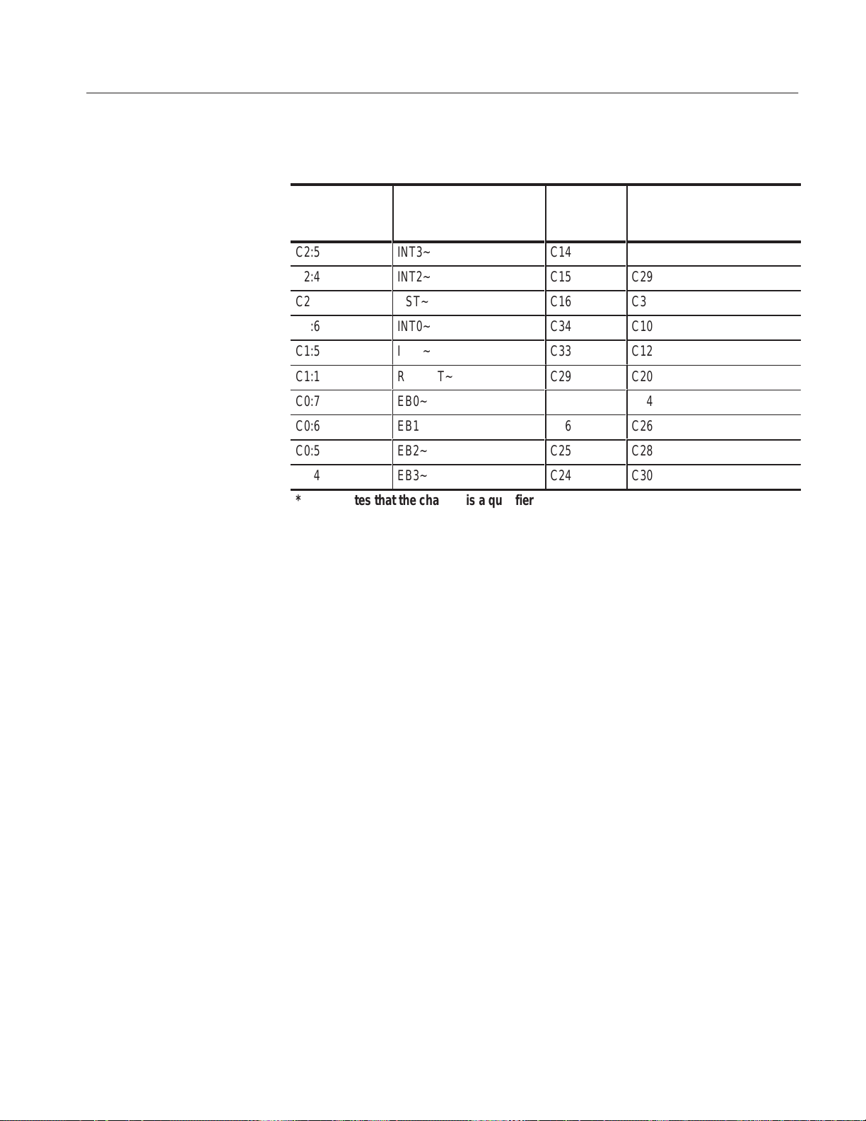
T able 5–14: CPU to Mictor connections for Mictor C pins (cont.)
Á
Á
Á
Á
Reference:Tables
MMC2107 support
LA channel
C2:5
C2:4
C2:3 *
C1:6
C1:5
C1:1
C0:7
ÁÁÁÁ
C0:6
C0:5
C0:4
channel name
INT3~
INT2~
RST~
INT0~
INT1~
RSTOUT~
EB0~
ББББББ
EB1~
EB2~
EB3~
* Indicates that the channel is a qualifier
Tektronix
mictor C
pin number
C14
C15
C16
C34
C33
C29
C27
ÁÁ
C26
C25
C24
AMP
mictor C
pin number
C27
C29
C31
C10
C12
C20
C24
БББББББ
C26
C28
C30
TMS230 MMC2107 Microcontroller Support
5–13
Page 54

Reference:Tables
5–14
TMS230 MMC2107 Microcontroller Support
Page 55

Index
Page 56

Page 57

Index
A
About this manual set, vii
Acquiring data, 2–5
Address, T ektronix, viii
Address group, channel assignments, 5–3
Application, logic analyzer configuration, 1–1
B
Base Address, 2–9
Bus cycles, displayed cycle types, 2–6
C
Channel assignments
address group, 5–3
chipselect group, 5–5
clocks and qualifiers, 5–6
control group, 5–5
data group, 5–4
misc group, 5–6
proc_mode group, 5–5
Channel groups, 2–1
visibility , 2–5
ChipSelect group, channel assignments, 5–5
Clock channel assignments, 5–6
Clock rate, SUT, 3–1
Clocking, custom, 2–2
Clocking Options
external clocking, 2–2
internal clocking, 2–2
Connections
cpu to mictor, 5–9
no probe adapter, 1–2
Contacting T ektronix, viii
Control flow display format, 2–7
Control group
channel assignments, 5–5
symbol table, 5–1
CPU to Mictor connections, 5–9
Custom clocking, 2–2
Cycle types, 2–6
D
Data
acquiring, 2–5
disassembly formats
control Flow, 2-7
hardware, 2-6
software, 2-7
subroutine, 2-8
timingĆDisplay, 2-6
Data display , changing, 2–8
Data group, channel assignments, 5–4
Data Port Width, 2–9
Definitions
disassembler, vii
information on basic operations, vii
Demonstration file, 2–10
Disassembled data
cycle type definitions, 2–6
viewing, 2–5
viewing an example, 2–10
Disassembler
definition, vii
logic analyzer configuration, 1–1
setup, 2–1
Disassembly format definition overlay, 2–8
Disassembly property page, 2–8
Display formats
control Flow, 2–7
hardware, 2–6
software, 2–7
special characters, 2–5
subroutine, 2–8
timing-Display, 2–6
E
Electrical specifications, 3–1
clock rate, SUT, 3–1
H
Hardware display format, 2–6
cycle type definitions, 2–6
Hold time, minimum, 3–1
TMS230 MMC2107 Microcontroller Support
Index–1
Page 58

Index
I
Installing support software, 2–1
L
Logic analyzer
configuration for disassembler, 1–1
configuration for the application, 1–1
software compatibility, 1–1
M
Manual
conventions, vii
how to use the set, vii
Mark Cycle function, 2–9
Mark Opcode function, 2–9
Marking cycles, definition of, 2–9
Micro Specific Fields
base address, 2–9
Data Port Width, 2–9
Mictor to CPU connections, 5–9
Misc group, channel assignments, 5–6
P
S
Service support, contact information, viii
Set up time, minimum, 3–1
Setups
disassembler, 2–1
support, 2–1
Signals not required for Clocking and Disassembly, 5–8
Signals required for Clocking and Disassembly, 5–7
Software display format, 2–7
Special characters displayed, 2–5
Specifications, 3–1
electrical, 3–1
Subroutine display format, 2–8
Support package setups
disassembly, 2–2
timing, 2–2
Support setup, 2–1
Symbol table, control channel group, 5–1
System file, demonstration, 2–10
T
T echnical support, contact information, viii
T ektronix, contacting, viii
T erminology, vii
Timing-display format, 2–6
Phone number, Tektronix, viii
Probe adapter, not using one, 1–2
Proc_Mode group, channel assignments, 5–5
Product support, contact information, viii
R
Reference, channel assignments, 5–2
Reference memory, 2–10
Restrictions, 1–1
without a probe adapter, 1–2
U
URL, T ektronix, viii
V
Viewing disassembled data, 2–5
W
Web site address, Tektronix, viii
Index–2
TMS230 MMC2107 Microcontroller Support
 Loading...