

Page 1

Instruction Manual
TMS 221
MCF5204 Microprocessor Support
071-0042-01
Warning
The servicing instructions are for use by
qualified personnel only. To avoid personal
injury, do not perform any servicing unless you
are qualified to do so. Refer to all safety
summaries prior to performing service.
Page 2

Copyright E T ektronix, Inc. All rights reserved. Licensed software products are owned by Tektronix or its suppliers and are
protected by United States copyright laws and international treaty provisions.
Use, duplication, or disclosure by the Government is subject to restrictions as set forth in subparagraph (c)(1)(ii) of the
Rights in T echnical Data and Computer Software clause at DFARS 252.227-7013, or subparagraphs (c)(1) and (2) of the
Commercial Computer Software – Restricted Rights clause at F AR 52.227-19, as applicable.
T ektronix products are covered by U.S. and foreign patents, issued and pending. Information in this publication supercedes
that in all previously published material. Specifications and price change privileges reserved.
Printed in the U.S.A.
T ektronix, Inc., P.O. Box 1000, Wilsonville, OR 97070–1000
TEKTRONIX and TEK are registered trademarks of T ektronix, Inc.
Page 3

SOFTWARE WARRANTY
T ektronix warrants that the media on which this software product is furnished and the encoding of the programs on
the media will be free from defects in materials and workmanship for a period of three (3) months from the date of
shipment. If a medium or encoding proves defective during the warranty period, T ektronix will provide a
replacement in exchange for the defective medium. Except as to the media on which this software product is
furnished, this software product is provided “as is” without warranty of any kind, either express or implied.
T ektronix does not warrant that the functions contained in this software product will meet Customer’s
requirements or that the operation of the programs will be uninterrupted or error-free.
In order to obtain service under this warranty, Customer must notify Tektronix of the defect before the expiration
of the warranty period. If T ektronix is unable to provide a replacement that is free from defects in materials and
workmanship within a reasonable time thereafter, Customer may terminate the license for this software product
and return this software product and any associated materials for credit or refund.
THIS WARRANTY IS GIVEN BY TEKTRONIX IN LIEU OF ANY OTHER WARRANTIES, EXPRESS
OR IMPLIED. TEKTRONIX AND ITS VENDORS DISCLAIM ANY IMPLIED WARRANTIES OF
MERCHANTABILITY OR FITNESS FOR A PARTICULAR PURPOSE. TEKTRONIX’
RESPONSIBILITY TO REPLACE DEFECTIVE MEDIA OR REFUND CUSTOMER’S PAYMENT IS
THE SOLE AND EXCLUSIVE REMEDY PROVIDED TO THE CUSTOMER FOR BREACH OF THIS
WARRANTY. TEKTRONIX AND ITS VENDORS WILL NOT BE LIABLE FOR ANY INDIRECT,
SPECIAL, INCIDENTAL, OR CONSEQUENTIAL DAMAGES IRRESPECTIVE OF WHETHER
TEKTRONIX OR THE VENDOR HAS ADVANCE NOTICE OF THE POSSIBILITY OF SUCH
DAMAGES.
Page 4

HARDWARE WARRANTY
T ektronix warrants that the products that it manufactures and sells will be free from defects in materials and
workmanship for a period of one (1) year from the date of shipment. If a product proves defective during this
warranty period, T ektronix, at its option, either will repair the defective product without charge for parts and labor,
or will provide a replacement in exchange for the defective product.
In order to obtain service under this warranty, Customer must notify Tektronix of the defect before the expiration
of the warranty period and make suitable arrangements for the performance of service. Customer shall be
responsible for packaging and shipping the defective product to the service center designated by T ektronix, with
shipping charges prepaid. Tektronix shall pay for the return of the product to Customer if the shipment is to a
location within the country in which the T ektronix service center is located. Customer shall be responsible for
paying all shipping charges, duties, taxes, and any other charges for products returned to any other locations.
This warranty shall not apply to any defect, failure or damage caused by improper use or improper or inadequate
maintenance and care. T ektronix shall not be obligated to furnish service under this warranty a) to repair damage
resulting from attempts by personnel other than T ektronix representatives to install, repair or service the product;
b) to repair damage resulting from improper use or connection to incompatible equipment; c) to repair any
damage or malfunction caused by the use of non-T ektronix supplies; or d) to service a product that has been
modified or integrated with other products when the effect of such modification or integration increases the time
or difficulty of servicing the product.
THIS WARRANTY IS GIVEN BY TEKTRONIX IN LIEU OF ANY OTHER WARRANTIES, EXPRESS
OR IMPLIED. TEKTRONIX AND ITS VENDORS DISCLAIM ANY IMPLIED WARRANTIES OF
MERCHANTABILITY OR FITNESS FOR A PARTICULAR PURPOSE. TEKTRONIX’
RESPONSIBILITY TO REPAIR OR REPLACE DEFECTIVE PRODUCTS IS THE SOLE AND
EXCLUSIVE REMEDY PROVIDED TO THE CUST OMER FOR BREACH OF THIS WARRANTY.
TEKTRONIX AND ITS VENDORS WILL NOT BE LIABLE FOR ANY INDIRECT , SPECIAL,
INCIDENTAL, OR CONSEQUENTIAL DAMAGES IRRESPECTIVE OF WHETHER TEKTRONIX OR
THE VENDOR HAS ADVANCE NOTICE OF THE POSSIBILITY OF SUCH DAMAGES.
Page 5

Table of Contents
Getting Started
Operating Basics
General Safety Summary v. . . . . . . . . . . . . . . . . . . . . . . . . . . . . . . . . . . . . . . . . . .
Service Safety Summary vii. . . . . . . . . . . . . . . . . . . . . . . . . . . . . . . . . . . . . . . . . . .
Preface: Microprocessor Support Documentation ix. . . . . . . . . . . . . . . .
Manual Conventions ix. . . . . . . . . . . . . . . . . . . . . . . . . . . . . . . . . . . . . . . . . . . . . .
Logic Analyzer Documentation x. . . . . . . . . . . . . . . . . . . . . . . . . . . . . . . . . . . . . .
Contacting T ektronix x. . . . . . . . . . . . . . . . . . . . . . . . . . . . . . . . . . . . . . . . . . . . . .
Support Description 1–1. . . . . . . . . . . . . . . . . . . . . . . . . . . . . . . . . . . . . . . . . . . . . . .
Logic Analyzer Software Compatibility 1–1. . . . . . . . . . . . . . . . . . . . . . . . . . . . . . .
Logic Analyzer Configuration 1–1. . . . . . . . . . . . . . . . . . . . . . . . . . . . . . . . . . . . . . .
Requirements And Restrictions 1–1. . . . . . . . . . . . . . . . . . . . . . . . . . . . . . . . . . . . . .
Configuring The Probe Adapter 1–2. . . . . . . . . . . . . . . . . . . . . . . . . . . . . . . . . . . . . .
Connecting To A System Under Test With A Probe Adapter 1–4. . . . . . . . . . . . . . .
Removing The Probe Adapter From The SUT 1–7. . . . . . . . . . . . . . . . . . . . . . .
Connecting To A System Under Test Without A Probe Adapter 1–7. . . . . . . . . . . . .
Channel Assignments 1–8. . . . . . . . . . . . . . . . . . . . . . . . . . . . . . . . . . . . . . . . . . . . .
CPU To Mictor Connections 1–12. . . . . . . . . . . . . . . . . . . . . . . . . . . . . . . . . . . . . . . .
Setting Up the Support 2–1. . . . . . . . . . . . . . . . . . . . . . . . . . . . . . . . . . . . . .
Channel Groups 2–1. . . . . . . . . . . . . . . . . . . . . . . . . . . . . . . . . . . . . . . . . . . . . . . . . .
How Data Is Acquired 2–1. . . . . . . . . . . . . . . . . . . . . . . . . . . . . . . . . . . . . . . . . . . . .
Clocking Options 2–1. . . . . . . . . . . . . . . . . . . . . . . . . . . . . . . . . . . . . . . . . . . . . . . . .
Custom Clocking 2–2. . . . . . . . . . . . . . . . . . . . . . . . . . . . . . . . . . . . . . . . . . . . . . . . .
Symbols 2–5. . . . . . . . . . . . . . . . . . . . . . . . . . . . . . . . . . . . . . . . . . . . . . . . . . . . . . . .
Acquiring And Viewing Disassembled Data 2–7. . . . . . . . . . . . . . . . . . . . .
Acquiring Data 2–7. . . . . . . . . . . . . . . . . . . . . . . . . . . . . . . . . . . . . . . . . . . . . . . . . . .
Viewing Disassembled Data 2–7. . . . . . . . . . . . . . . . . . . . . . . . . . . . . . . . . . . . . . . .
Hardware Display Format 2–8. . . . . . . . . . . . . . . . . . . . . . . . . . . . . . . . . . . . . . .
Software Display Format 2–9. . . . . . . . . . . . . . . . . . . . . . . . . . . . . . . . . . . . . . .
Control Flow Display Format 2–9. . . . . . . . . . . . . . . . . . . . . . . . . . . . . . . . . . . .
Subroutine Display Format 2–10. . . . . . . . . . . . . . . . . . . . . . . . . . . . . . . . . . . . . .
Changing How Data is Displayed 2–10. . . . . . . . . . . . . . . . . . . . . . . . . . . . . . . . . . .
Optional Display Selections 2–11. . . . . . . . . . . . . . . . . . . . . . . . . . . . . . . . . . . . .
Marking Cycles 2–12. . . . . . . . . . . . . . . . . . . . . . . . . . . . . . . . . . . . . . . . . . . . . . .
Displaying Exception Vectors 2–13. . . . . . . . . . . . . . . . . . . . . . . . . . . . . . . . . . . .
TMS 221 MCF5204 Microprocessor Support Instruction Manual
i
Page 6

Table of Contents
Specifications
Specification Tables 3–1. . . . . . . . . . . . . . . . . . . . . . . . . . . . . . . . . . . . . . . . . . . . . . .
Maintenance
Probe Adapter Description 4–1. . . . . . . . . . . . . . . . . . . . . . . . . . . . . . . . . . . . . . . . . .
Replacing Signal Leads 4–1. . . . . . . . . . . . . . . . . . . . . . . . . . . . . . . . . . . . . . . . . . . .
Replaceable Electrical Parts
Parts Ordering Information 5–1. . . . . . . . . . . . . . . . . . . . . . . . . . . . . . . . . . . . . . . . .
Using the Replaceable Electrical Parts List 5–1. . . . . . . . . . . . . . . . . . . . . . . . . . . . .
Diagrams and Circuit Board Illustrations 5–5. . . . . . . . . . . . . . . . . . . . . .
Symbols 5–5. . . . . . . . . . . . . . . . . . . . . . . . . . . . . . . . . . . . . . . . . . . . . . . . . . . . . . . .
Component Values 5–5. . . . . . . . . . . . . . . . . . . . . . . . . . . . . . . . . . . . . . . . . . . . . . . .
Graphic Items and Special Symbols Used in This Manual 5–5. . . . . . . . . . . . . . . . .
Component Locator Diagrams 5–5. . . . . . . . . . . . . . . . . . . . . . . . . . . . . . . . . . . . . . .
Replaceable Mechanical Parts
Index
Parts Ordering Information 6–1. . . . . . . . . . . . . . . . . . . . . . . . . . . . . . . . . . . . . . . . .
Using the Replaceable Mechanical Parts List 6–1. . . . . . . . . . . . . . . . . . . . . . . . . . .
ii
TMS 221 MCF5204 Microprocessor Support Instruction Manual
Page 7

List of Figures
List of Tables
Table of Contents
Figure 1–1: Connecting the test clip to the probe adapter 1–4. . . . . . . . .
Figure 1–2: Connecting P6434 probes to the probe adapter 1–5. . . . . . . .
Figure 1–3: Placing the probe adapter onto the SUT 1–6. . . . . . . . . . . . .
Figure 1–4: Pin assignments for a Mictor connector (component side) 1–13. . .
Figure 2–1: MCF5204 Read/Write bus timing with external terminination
and one wait state 2–4. . . . . . . . . . . . . . . . . . . . . . . . . . . . . . . . . . . . . . .
Figure 2–2: MCF5204 Burst cycle bus timing with one wait state 2–5. . .
Figure 2–3: Hardware display format 2–9. . . . . . . . . . . . . . . . . . . . . . . . . .
Figure 3–1: Dimensions of the probe adapter 3–4. . . . . . . . . . . . . . . . . . . .
Figure 3–2: Dimensions of the test clip 3–5. . . . . . . . . . . . . . . . . . . . . . . . .
Table 1–1: DIP switch settings 1–2. . . . . . . . . . . . . . . . . . . . . . . . . . . . . . . .
Table 1–2: Address group channel assignments 1–8. . . . . . . . . . . . . . . . .
Table 1–3: Data group channel assignments 1–9. . . . . . . . . . . . . . . . . . . .
Table 1–4: Control group channel assignments 1–10. . . . . . . . . . . . . . . . . .
Table 1–5: Chip Select group channel assignments 1–10. . . . . . . . . . . . . . .
Table 1–6: Intr group channel assignments 1–10. . . . . . . . . . . . . . . . . . . . .
Table 1–7: Misc group channel assignments 1–11. . . . . . . . . . . . . . . . . . . .
Table 1–8: Clock channel assignments 1–11. . . . . . . . . . . . . . . . . . . . . . . . .
Table 1–9: BDM connector pinout 1–12. . . . . . . . . . . . . . . . . . . . . . . . . . . . .
Table 1–10: CPU to Mictor connections for Mictor A pins 1–13. . . . . . . .
Table 1–11: CPU to Mictor connections for Mictor C pins 1–15. . . . . . . .
Table 1–12: CPU to Mictor connections for Mictor D pins 1–16. . . . . . . .
Table 2–1: Control group symbol table definitions 2–5. . . . . . . . . . . . . . .
Table 2–2: Chip Select group symbol table definitions 2–6. . . . . . . . . . . .
Table 2–3: Meaning of special characters in the display 2–7. . . . . . . . . .
Table 2–4: Cycle type definitions 2–8. . . . . . . . . . . . . . . . . . . . . . . . . . . . .
Table 2–5: Exception vectors 2–13. . . . . . . . . . . . . . . . . . . . . . . . . . . . . . . . .
Table 3–1: Electrical specifications 3–1. . . . . . . . . . . . . . . . . . . . . . . . . . . .
Table 3–2: Environmental specifications 3–3. . . . . . . . . . . . . . . . . . . . . . .
TMS 221 MCF5204 Microprocessor Support Instruction Manual
iii
Page 8

Table of Contents
iv
TMS 221 MCF5204 Microprocessor Support Instruction Manual
Page 9

General Safety Summary
Review the following safety precautions to avoid injury and prevent damage to
this product or any products connected to it. To avoid potential hazards, use this
product only as specified.
Only qualified personnel should perform service procedures.
While using this product, you may need to access other parts of the system. Read
the General Safety Summary in other system manuals for warnings and cautions
related to operating the system.
To Avoid Fire or
Personal Injury
Connect and Disconnect Properly . Do not connect or disconnect probes or test
leads while they are connected to a voltage source.
Ground the Product. This product is indirectly grounded through the grounding
conductor of the mainframe power cord. To avoid electric shock, the grounding
conductor must be connected to earth ground. Before making connections to the
input or output terminals of the product, ensure that the product is properly
grounded.
Observe All Terminal Ratings. To avoid fire or shock hazard, observe all ratings
and marking on the product. Consult the product manual for further ratings
information before making connections to the product.
Do Not Operate Without Covers. Do not operate this product with covers or panels
removed.
Avoid Exposed Circuitry. Do not touch exposed connections and components
when power is present.
Do Not Operate With Suspected Failures. If you suspect there is damage to this
product, have it inspected by qualified service personnel.
Do Not Operate in Wet/Damp Conditions.
Do Not Operate in an Explosive Atmosphere.
Keep Product Surfaces Clean and Dry .
Provide Proper Ventilation. Refer to the manual’s installation instructions for
details on installing the product so it has proper ventilation.
TMS 221 MCF5204 Microprocessor Support Instruction Manual
v
Page 10
General Safety Summary
Symbols and Terms
T erms in this Manual. These terms may appear in this manual:
WARNING. Warning statements identify conditions or practices that could result
in injury or loss of life.
CAUTION. Caution statements identify conditions or practices that could result in
damage to this product or other property.
T erms on the Product. These terms may appear on the product:
DANGER indicates an injury hazard immediately accessible as you read the
marking.
WARNING indicates an injury hazard not immediately accessible as you read the
marking.
CAUTION indicates a hazard to property including the product.
Symbols on the Product. The following symbols may appear on the product:
WARNING
High Voltage
Protective Ground
(Earth) T erminal
CAUTION
Refer to Manual
Double
Insulated
vi
TMS 221 MCF5204 Microprocessor Support Instruction Manual
Page 11

Service Safety Summary
Only qualified personnel should perform service procedures. Read this Service
Safety Summary and the General Safety Summary before performing any service
procedures.
Do Not Service Alone. Do not perform internal service or adjustments of this
product unless another person capable of rendering first aid and resuscitation is
present.
Disconnect Power. To avoid electric shock, disconnect the main power by means
of the power cord or, if provided, the power switch.
Use Care When Servicing With Power On. Dangerous voltages or currents may
exist in this product. Disconnect power, remove battery (if applicable), and
disconnect test leads before removing protective panels, soldering, or replacing
components.
To avoid electric shock, do not touch exposed connections.
TMS 221 MCF5204 Microprocessor Support Instruction Manual
vii
Page 12

Service Safety Summary
viii
TMS 221 MCF5204 Microprocessor Support Instruction Manual
Page 13

Preface: Microprocessor Support Documentation
This instruction manual contains specific information about the TMS 221
MCF5204 microprocessor support package and is part of a set of information on
how to operate this product on compatible Tektronix logic analyzers.
If you are familiar with operating microprocessor support packages on the logic
analyzer for which the TMS 221 MCF5204 support was purchased, you will
probably only need this instruction manual to set up and run the support.
If you are not familiar with operating microprocessor support packages, you will
need to supplement this instruction manual with information on basic operations
to set up and run the support.
Information on basic operations of microprocessor support packages is included
with each product. Each logic analyzer has basic information describing how to
perform tasks common to support packages on that platform. This information
can be in the form of online help, an installation manual, or a user manual.
This manual provides detailed information on the following topics:
H Connecting the logic analyzer to your system under test
Manual Conventions
H Setting up the logic analyzer to acquire data
H Acquiring and viewing disassembled data
This manual uses the following conventions:
H The term “disassembler” refers to the software that disassembles bus cycles
into instruction mnemonics and cycle types.
H The phrase “information on basic operations” refers to online help, an
installation manual, or a basic operations of microprocessor supports user
manual.
H The term “MCF5204” refers to all supported variations of the MCF5204
microprocessor unless otherwise noted.
H In the information on basic operations, the term “XXX” or “P54C” used in
field selections and file names must be replaced with MCF5204. This is the
name of the microprocessor in field selections and file names you must use
to operate the MCF5204 support.
TMS 221 MCF5204 Microprocessor Support Instruction Manual
ix
Page 14

Preface: Microprocessor Support Documentation
H The term “logic analyzer” refers to the Tektronix logic analyzer for which
this product was purchased.
H The term “SUT” (system under test) refers to the microprocessor-based
system from which data will be acquired.
H An asterisk (*) following a signal name indicates an active low signal.
Logic Analyzer Documentation
A description of other documentation available for each type of Tektronix logic
analyzer is located in the corresponding module user manual. The manual set
provides the information necessary to install, operate, maintain, and service the
logic analyzer and associated products.
Contacting Tektronix
Product
Support
Service
Support
For other
information
To write us
Website
For questions about using T ektronix measurement products, call toll
free in North America:
1-800-TEK-WIDE (1-800-835-9433 ext. 2400)
6:00 a.m. – 5:00 p.m. Pacific time
Or contact us by e-mail:
tm_app_supp@tek.com
For product support outside of North America, contact your local
T ektronix distributor or sales office.
T ektronix offers extended warranty and calibration programs as options
on many products. Contact your local T ektronix distributor or sales
office.
For a listing of worldwide service centers, visit our web site.
In North America:
1-800-TEK-WIDE (1-800-835-9433)
An operator will direct your call.
T ektronix, Inc.
P.O. Box 1000
Wilsonville, OR 97070-1000
USA
T ektronix.com
x
TMS 221 MCF5204 Microprocessor Support Instruction Manual
Page 15

Getting Started
Page 16

Page 17

Getting Started
This chapter contains information on the TMS 221 microprocessor support, and
information on connecting your logic analyzer to your system under test.
Support Description
The TMS 221 microprocessor support package disassembles data from systems
that are based on the Motorola MCF5204 microprocessor.
The TMS 221 supports the MCF5204 microprocessor in a 100-pin TQFP
package.
To use this support efficiently, you need to have the items listed in the
information on basic operations as well as the MCF5204 User’s Manual,
Motorola, 1995.
Logic Analyzer Software Compatibility
The label on the microprocessor support floppy disk states which version of logic
analyzer software the support is compatible with.
Logic Analyzer Configuration
For use with a TLA 700 Series the TMS 221 support requires a minimum of
one 98-channel module.
For use with a DAS 9200 Series the TMS 221 support requires a minimum of
one 96-channel module.
Requirements And Restrictions
You should review the general requirements and restrictions of microprocessor
supports in the information on basic operations as they pertain to your system
under test.
You should review electrical, environmental, and mechanical specifications in the
Specifications chapter in this manual as they pertain to your system under test, as
well as the following descriptions of other MCF5204 support requirements and
restrictions.
TMS 221 MCF5204 Microprocessor Support Instruction Manual
1–1
Page 18

Getting Started
System Clock Rate. The TMS 221 support can acquire data from the MCF5204
1
microprocessor at speeds of up to 33 MHz
; it has been tested to 25 MHz.
Hardware Reset. If a hardware reset occurs in your MCF5204 system during an
acquisition, the disassembler may acquire an invalid sample.
Cache Invalidation. Correct disassembly is not guaranteed for microprocessor
systems that run cache invalidations concurrent with burst cycles. Data for these
cycles will not be disassembled and will be labeled as Cache Invalidation cycles.
Disabling The Internal Cache. To disassemble acquired data, you must disable the
internal cache. Disabling the cache makes all instruction prefetches visible on the
bus so they can be acquired and disassembled.
Big-Endian Byte Ordering. The disassembler always uses Big-Endian byte
ordering for instruction disassembly. Big-Endian byte ordering is when the most
significant data byte is located at the highest address.
Data Reads And Writes. The disassembler will not link data reads and writes with
the instructions which cause them.
Configuring The Probe Adapter
Configuring The Chip Select Module Switch. The probe adapter has a DIP switch
that must be set according to the chip select module configuration of the
MCF5204. Use Table 1–1 to configure the chip select DIP switch. By default all
switches are off.
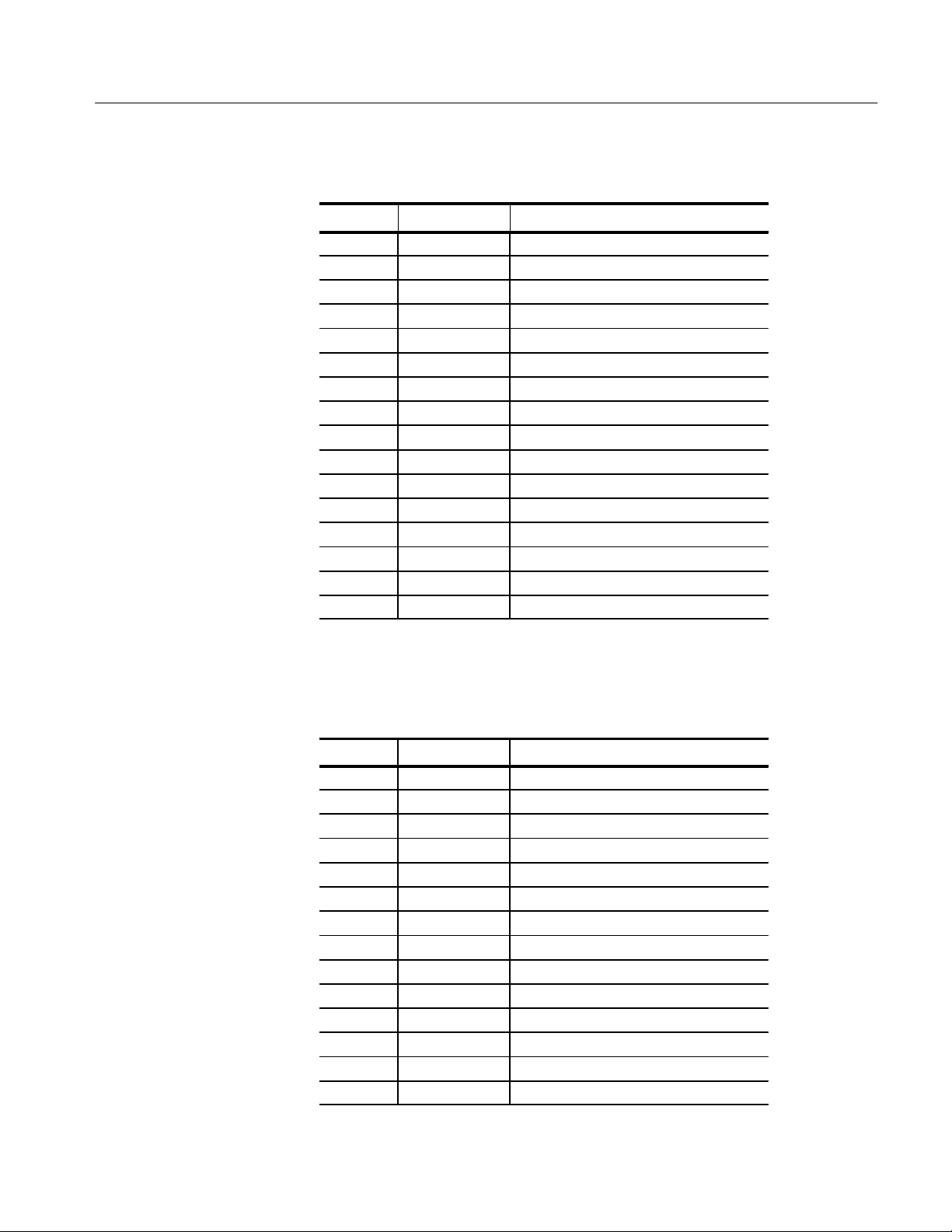
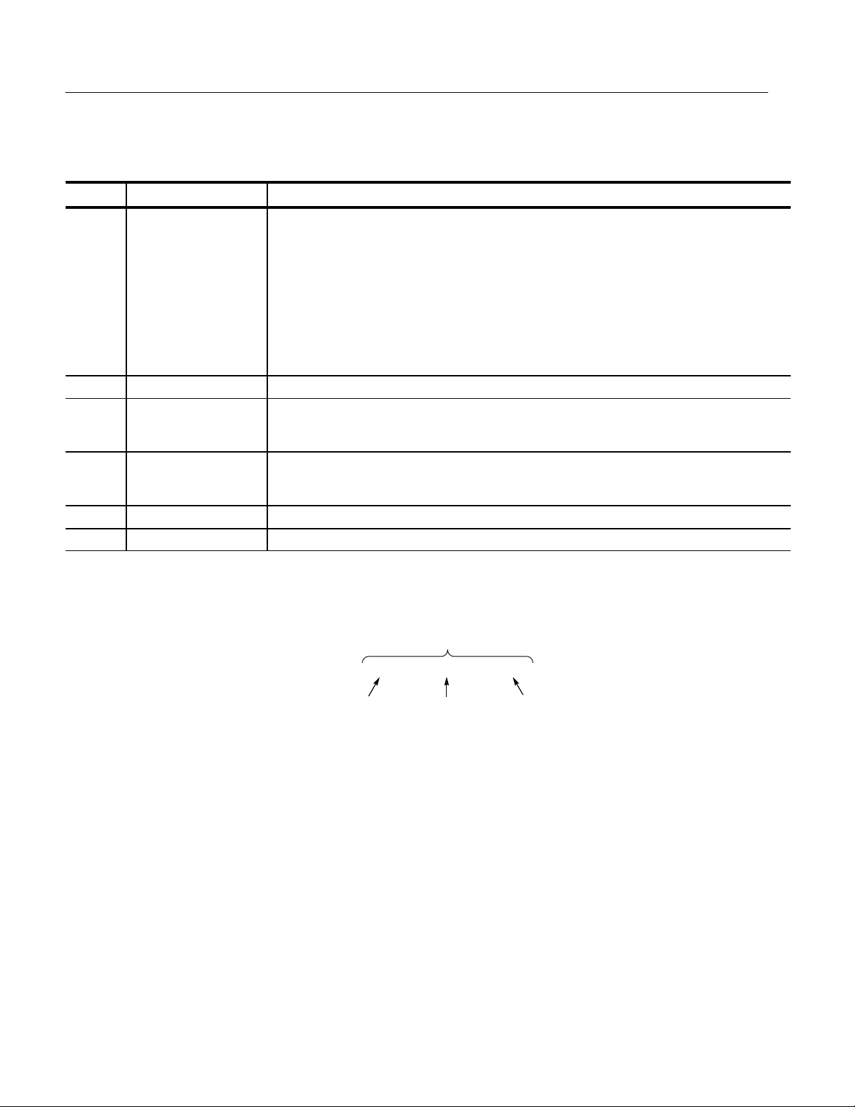
T able 1–1: DIP switch settings
Switch Description
S1 CS0*
S2 CS1*
S3 CS2*
S4 CS3*
S5 CS4*
S6 CS5*
1
Specification at time of printing. Contact your Tektronix sales representative for
current information on the fastest devices supported.
1–2
TMS 221 MCF5204 Microprocessor Support Instruction Manual
Page 19

Getting Started
T able 1–1: DIP switch settings (cont.)
Switch Description
S7 Not used
S8 Not used
Examples Of Switch Settings. The following example shows two possible settings:
Please note: S1 is closest to the S100 silk screen, and the ON position is the
position closest to the edge of the probe adapter.
H Example 1
If CS0*, CS3* and CS5* are configured for zero wait state, and CS1*, CS2*
and CS4* are configured for non-zero wait state, the DIP switch settings
would be:
S1 – ON (CS0*)
S2 – OFF (CS1*)
S3 – OFF (CS2*)
S4 – ON (CS3*)
S5 – OFF (CS4*)
S6 – ON (CS5*)
S7 – Not used
S8 – Not used
H Example 2
If CS0* is configured for asynchronous transfer mode, CS1* and CS2* are
configured with 3-wait states, CS3* is configured for zero wait state, and
CS4* and CS5* are not used, the DIP switch settings would be:
S1 – OFF (CS0*)
S2 – OFF (CS1*)
S3 – OFF (CS2*)
S4 – ON (CS3*)
S5 – OFF (CS4*)
S6 – OFF (CS5*)
S7 – Not used
S8 – Not used
TMS 221 MCF5204 Microprocessor Support Instruction Manual
1–3
Page 20
Getting Started
Connecting To A System Under Test With A Probe Adapter
To connect the logic analyzer to a SUT (system under test) using the probe
adapter and test clip, follow these steps:
1. Turn off power to your SUT.
It is not necessary to turn off the logic analyzer.
CAUTION. Static discharge can damage the microprocessor, the probe adapter,
the probes, or the module. To prevent static damage, handle all the above only in
a static-free environment.
Always wear a grounding wrist strap or similar device while handling the
microprocessor and probe adapter.
2. To discharge your stored static electricity, touch the ground connector located
on the logic analyzer.
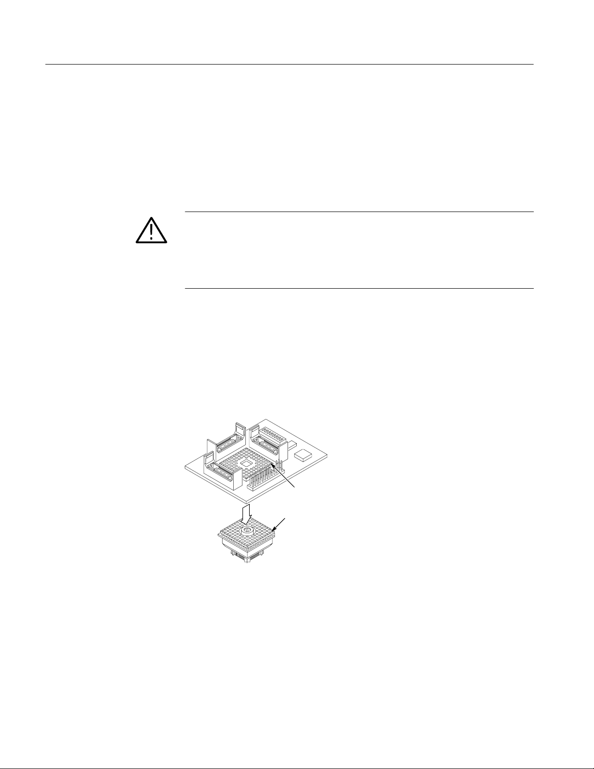
Connect The Test Clip To
The Probe Adapter
To connect the test clip to the probe adapter follow these steps:
3. Line up pin 1 on the test clip, to pin 1 on the connector located on the bottom
of the probe adapter circuit board, as shown in Figure 1–1.
Pin 1
Pin 1
Figure 1–1: Connecting the test clip to the probe adapter
1–4
TMS 221 MCF5204 Microprocessor Support Instruction Manual
Page 21

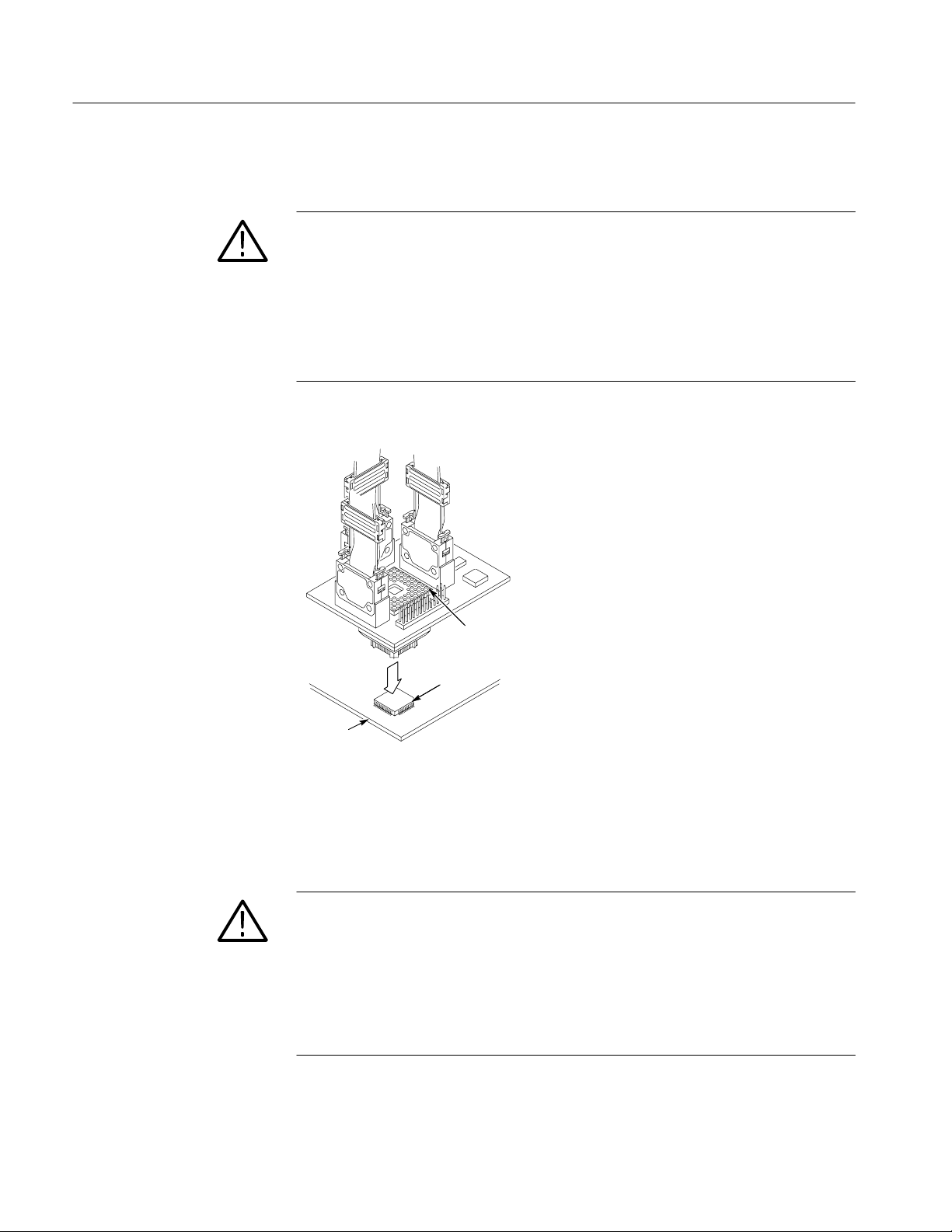
Getting Started
Connect The P6434
Probes To The Probe
Adapter
To connect the P6434 probes to the probe adapter follow these steps:
CAUTION. Incorrect handling of the P6434 probe while connecting it to the probe
adapter can result in damage to the probe or to the mating connector on the
probe adapter. To avoid damaging the probe and probe adapter, always position
the probe perpendicular to the mating connector and gently connect the probe.
4. Refer to Figure 1–2, and connect the P6434 probes to the probe adapter.
Match the channel groups and numbers on the probe labels to the corre-
sponding connectors on the probe adapter.
5. Position the probe tip perpendicular to the mating connector and gently
connect the probe as shown in Figure 1–2.
6. When connected, push down the latch releases on the probe to set the latch.
Push down to latch after
probe is connected
Push down to latch after
probe is connected
Connect The Probe
Adapter Assembly To The
System Under Test
Pin 1
Pin 1
Figure 1–2: Connecting P6434 probes to the probe adapter
To connect the probe adapter assembly (probe adapter and test clip) to your SUT
follow these instructions:
7. Inspect the microprocessor on you SUT for bent or broken leads. Verify that
the leads on the microprocessor are clean and free from dirt, dust, or any
foreign material.
8. Inspect the pins of the test clip for bent or broken contacts. Verify that the
leads on the test clip are clean and free from dirt, dust or any foreign
material.
9. Verify that the locking devise on the test clip is not locked by turning the
locking device counter-clockwise with a small screwdriver .
TMS 221 MCF5204 Microprocessor Support Instruction Manual
1–5
Page 22
Getting Started
10. Place the probe adapter onto the SUT as shown in Figure 1–3.
CAUTION. Failure to correctly place the probe adapter onto the microprocessor
might permanently damage all electrical components when power is applied.
Center the clip on the microprocessor and apply an equal downward force on all
four sides of the clip. It is important to keep the TQFP test clip parallel to the
microprocessor to avoid damage to the SUT or TQFP test clip.
Do not apply leverage to the probe adapter when installing or removing it.
Pin 1
Pin 1
SUT
Figure 1–3: Placing the probe adapter onto the SUT
11. Lock the test clip to the microprocessor by turning the locking knob
clockwise with a small screwdriver.
CAUTION. The test clip was designed to be used on one and only one microprocessor. Because of the tight tolerances required for QFP test clip connectivity, the
test clip that attaches to the microprocessor has a soft plastic collar that
conforms to the unique shape of the target microprocessor.
To avoid faulty and unreliable connections, it is HIGHLY recommended that the
test clip IS NOT used on any other microprocessor then the one it was originally
connected to.
1–6
TMS 221 MCF5204 Microprocessor Support Instruction Manual
Page 23
Getting Started
CAUTION. The probe adapter board might slip off or slip to one side of the
microprocessor because of the extra weight of the probes. This can damage the
microprocessor
To prevent this from occurring, stabilize the probe adapter by placing a
non-conductive object (such as non-conductive foam) between the probe adapter
and the SUT.
and the SUT.
Removing The Probe
Adapter From The SUT
To remove the probe adapter from the sut follow these steps:
1. Unlock the test clip from the microprocessor by turning the locking knob
counter-clockwise with a small screwdriver.
2. Gently lift and pull the probe adapter off of the microprocessor.
Connecting To A System Under Test Without A Probe Adapter
You can use the channel and clock probes and leadsets with a commercial test
clip (or adapter) to make connections between the logic analyzer and your SUT.
To connect probes to MCF5204 signals in the SUT using a test clip, follow these
steps:
1. Turn off power to your SUT. It is not necessary to turn off power to the logic
analyzer.
CAUTION. Static discharge can damage the microprocessor, the probes, or the
module. To prevent static damage, handle all of the above only in a static-free
environment.
Always wear a grounding wrist strap or similar device while handling the
microprocessor.
2. To discharge your stored static electricity, touch the ground connector located
on the back of the logic analyzer. If you are using a test clip, touch any of the
ground pins on the clip to discharge stored static electricity from it.
3. Table 1–2 through Table 1–8 lists the channel probes the MCF5204 signal
pins on the test clip or in the SUT to connect to.
Use leadsets to connect at least one ground lead from each channel probe and
the ground lead from each clock probe to ground pins on your test clip.
4. Align pin 1 or A1 of your test clip with the corresponding pin 1 or A1 of the
MCF5204 microprocessor in your SUT and attach the clip.
TMS 221 MCF5204 Microprocessor Support Instruction Manual
1–7
Page 24

Getting Started
Channel Assignments
The following channel assignment tables show the probe section and channel
assignments, and the signal to which each channel connects.
Channel assignments shown in Table 1–2 through Table 1–8 use the following
conventions:
H All signals are required by the support unless indicated otherwise.
H Channels are shown starting with the most significant bit (MSB) descending
to the least significant bit (LSB).
H Channel group assignments are for all modules unless otherwise noted.
H An asterisk (*) following a signal name indicates an active low signal.
H An equals sign (=) following a signal name indicates that it is double probed.
By default, the Address group is displayed in hexadecimal.
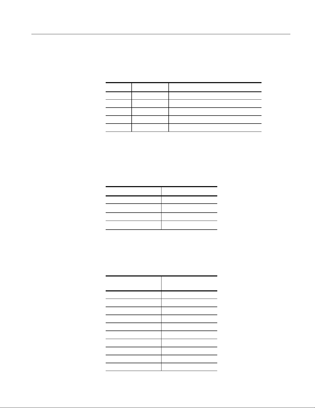
T able 1–2: Address group channel assignments
Bit order Section:channel MCF5204 signal name
31 A3:7 NC
30 A3:6 NC
29 A3:5 NC
28 A3:4 NC
27 A3:3 NC
26 A3:2 NC
25 A3:1 NC
24 A3:0 NC
23 A2:7 NC
22 A2:6 NC
21 A2:5 A21/PP1
20 A2:4 A20/PP0
19 A2:3 A19
18 A2:2 A18
17 A2:1 A17
16 A2:0 A16
1–8
TMS 221 MCF5204 Microprocessor Support Instruction Manual
Page 25
T able 1–2: Address group channel assignments (cont.)
Bit order MCF5204 signal nameSection:channel
15 A1:7 A15
14 A1:6 A14
13 A1:5 A13
12 A1:4 A12
11 A1:3 A11
10 A1:2 A10
9 A1:1 A9
8 A1:0 A8
7 A0:7 A7
6 A0:6 A6
5 A0:5 A5
4 A0:4 A4
3 A0:3 A3
2 A0:2 A2
1 A0:1 A1
0 A0:0 A0
Getting Started
By default, the Data group is displayed in hexadecimal.
T able 1–3: Data group channel assignments
Bit order Section:channel MCF5204 signal name
15 D1:7 D15
14 D1:6 D14
13 D1:5 D13
12 D1:4 D12
11 D1:3 D11
10 D1:2 D10
9 D1:1 D9
8 D1:0 D8
7 D0:7 D7
6 D0:6 D6
5 D0:5 D5
4 D0:4 D4
3 D0:3 D3
2 D0:2 D2
TMS 221 MCF5204 Microprocessor Support Instruction Manual
1–9
Page 26

Getting Started
T able 1–3: Data group channel assignments (cont.)
Bit order MCF5204 signal nameSection:channel
1 D0:1 D1
0 D0:0 D0
By default, the Control group is displayed symbolically. The symbol
table file name is 5204_Ctrl.
T able 1–4: Control group channel assignments
Bit order Section:channel MCF5204 signal name
2 C2:3 RESET*
1 C2:1 RE*
0 C2:2 WE*
By default, the Chip Select (Chip_Sel) group is displayed in binary.
The symbol table file name is 5204_CS.
T able 1–5: Chip Select group channel assignments
Bit order Section:channel MCF5204 signal name
5 C3:7 CS5*
4 C3:6 CS4*
3 C3:5 CS3*
2 C3:4 CS2*
1 C3:3 CS1*
0 C3:2 CS0*
By default, the Intr group is not visible.
T able 1–6: Intr group channel assignments
Bit order Section:channel MCF5204 signal name
3 C1:7
2 C1:6
1 C1:5
0 C1:4
[ Signal not required for disassembly.
IRQ3* [
IRQ2* [
IRQ1* [
IRQ0 [
1–10
TMS 221 MCF5204 Microprocessor Support Instruction Manual
Page 27
Getting Started
By default, the Misc group is not visible.
T able 1–7: Misc group channel assignments
Bit order Section:channel MCF5204 signal name
4 C3:1 CLK
3 C3:0
2 C2:0 DTACK*
1 C2:7
0 C2:6
[ Signal not required for disassembly.
ATS* [
UWE*/UDS* [
LWE*/LDS* [
Table 1–8 lists the probe section and channel assignments for the clock probes.
The clock probes are not part of any group.
T able 1–8: Clock channel assignments
Section:channel MCF5204 signal name
CK:0 CLK =
CK:1 ZERO*
CK:2 A0 =
CK:3 A1 =
Table 1–9 lists the pinout of J320, the Background Debug Mode (BDM)
connector.
T able 1–9: BDM connector pinout
BDM connector pin
MCF5204 signal name
NC (Developer Reserved) 1
BKPT* 2
GND 3
DSCLK 4
GND 5
NC (Developer Reserved) 6
RESET* 7
DSI 8
VCC (+5V) w
DSO 10
number
9
TMS 221 MCF5204 Microprocessor Support Instruction Manual
1–11
Page 28

Getting Started
T able 1–9: BDM connector pinout
BDM connector pin
MCF5204 signal name
GND 11
PST3 12
PST2 13
PST1 14
PST0 15
DDA TA3 16
DDA TA2 17
DDA TA1 18
DDA TA0 19
GND 20
NC (Motorola reserved) 21
NC (Motorola reserved) 22
GND 23
CLK_CPU ]
Vcc_CPU w
NC 26
] Connected to CLK on the microprocessor.
number
24
25
w Connected to Vcc on the probe adapter.
CPU To Mictor Connections
To probe the microprocessor you will need to make connections between the
CPU and the Mictor pins of the P6434 Mass Termination Probe. Refer to the
P6434 Mass Termination Probe manual, Tektronix part number 070-9793-xx, for
more information on mechanical specifications. Table 1–10 through Table 1–12
show the CPU pin to Mictor pin connections.
Tektronix uses a counter-clockwise pin assignment. Pin-1 is located at the top
left, and pin-2 is located directly below it. Pin-20 is located on the bottom right,
and pin-21 is located directly above it.
AMP uses an odd side-even side pin assignment. Pin-1 is located at the top left,
and pin-3 is located directly below it. Pin-2 is located on the top right, and pin-4
is located directly below it.
1–12
TMS 221 MCF5204 Microprocessor Support Instruction Manual
Page 29

Getting Started
NOTE. When designing Mictor connectors into your SUT, always follow the
Tektronix pin assignment.
Tektronix Pinout AMP Pinout
Pin 1
Pin 19
Pin 38
Pin 20
Pin 1
Pin 37
Pin 2
Pin 38
Figure 1–4: Pin assignments for a Mictor connector (component side)
Please pay close attention to the caution below.
CAUTION. To protect the CPU and the inputs of the module, it is recommended
that a 180W resistor is connected in series between each ball pad of the CPU and
each pin of the Mictor connector. The resistor must be no farther away from the
ball pad of the CPU than 1/2-inch.
T able 1–10: CPU to Mictor connections for Mictor A pins
Tektronix
Mictor A
pin number
1 1 NC NC NC
2 3 NC NC NC
3 5 CLOCK:0 CLK= 87
4 7 A3:7 Not Used Not Used
5 9 A3:6 Not Used Not Used
6 11 A3:5 Not Used Not Used
7 13 A3:4 Not Used Not Used
8 15 A3:3 Not Used Not Used
9 17 A3:2 Not Used Not Used
10 19 A3:1 Not Used Not Used
11 21 A3:0 Not Used Not Used
12 23 A2:7 Not Used Not Used
13 25 A2:6 Not Used Not Used
14 27 A2:5 A21 28
AMP
Mictor A
pin number
LA channel MCF5204 signal name
MCF5204
pin number
TMS 221 MCF5204 Microprocessor Support Instruction Manual
1–13
Page 30

Getting Started
T able 1–10: CPU to Mictor connections for Mictor A pins (cont.)
Tektronix
Mictor A
pin number
15 29 A2:4 A20 27
16 31 A2:3 A19 26
17 33 A2:2 A18 25
18 35 A2:1 A17 22
19 37 A2:0 A16 21
20 38 A0:0 A0 99
21 36 A0:1 A1 100
22 34 A0:2 A2 1
23 32 A0:3 A3 4
24 30 A0:4 A4 5
25 28 A0:5 A5 6
26 26 A0:6 A6 7
27 24 A0:7 A7 8
28 22 A1:0 A8 11
29 20 A1:1 A9 12
30 18 A1:2 A10 13
31 16 A1:3 A11 14
32 14 A1:4 A12 15
33 12 A1:5 A13 18
34 10 A1:6 A14 19
35 8 A1:7 A15 20
36 6 CLOCK:1 Not Used
37 4 NC NC NC
38 2 NC NC NC
39 39 GND GND GND
40 40 GND GND GND
41 41 GND GND GND
42 42 GND GND GND
43 43 GND GND GND
= Double probe
AMP
Mictor A
pin number
MCF5204
MCF5204 signal nameLA channel
pin number
w
1–14
TMS 221 MCF5204 Microprocessor Support Instruction Manual
Page 31

T able 1–11: CPU to Mictor connections for Mictor C pins
Getting Started
TektronixMictor C
pin number
1 1 NC NC NC
2 3 NC NC NC
3 5 CLOCK:3 A1= 100
4 7 C3:7 CS5* 92
5 9 C3:6 CS4* 91
6 11 C3:5 CS3* 90
7 13 C3:4 CS2* 36
8 15 C3:3 CS1* 35
9 17 C3:2 CS0* 34
10 19 C3:1 CLK 87
11 21 C3:0 ATS* 50
12 23 C2:7 UWE*/UDS* 43
13 25 C2:6 LWE*/LDS* 44
14 27 C2:5 TIN/PP2 32
15 29 C2:4 TOUT/PP3 33
16 31 C2:3 RESET* 77
17 33 C2:2 WE* 29
18 35 C2:1 RE* 47
19 37 C2:0 DTACK* 51
20 38 C0:0 Not Used Not Used
21 36 C0:1 Not Used Not Used
22 34 C0:2 MTMOD3 89
23 32 C0:3 TCLK 76
24 30 C0:4 DSCLK/TRST 86
25 28 C0:5 DSI/TDI 85
26 26 C0:6 DSO/TDO 84
27 24 C0:7 BKPT*/TMS 88
28 22 C1:0 TXD/PP4 41
29 20 C1:1 RXD/PP5 42
30 18 C1:2 CTS*/PP6 48
31 16 C1:3 RTS*/PP7 49
32 14 C1:4 IRQ0* 37
33 12 C1:5 IRQ1* 38
34 10 C1:6 IRQ2* 39
35 8 C1:7 IRQ3* 40
AMP
Mictor C
pin number
LA channel MCF5204 signal name
MCF5204
pin number
TMS 221 MCF5204 Microprocessor Support Instruction Manual
1–15
Page 32
Getting Started
T able 1–11: CPU to Mictor connections for Mictor C pins (cont.)
TektronixMictor C
pin number
36 6 NC NC GND
37 4 NC NC NC
38 2 NC NC NC
39 39 GND GND GND
40 40 GND GND GND
41 41 GND GND GND
42 42 GND GND GND
43 43 GND GND GND
= Double probe
AMP
Mictor C
pin number
MCF5204
MCF5204 signal nameLA channel
pin number
T able 1–12: CPU to Mictor connections for Mictor D pins
Tektronix
Mictor D
pin number
1 1 NC NC NC
2 3 NC NC NC
3 5 NC NC NC
4 7 D3:7 PST3 83
5 9 D3:6 PST2 82
6 11 D3:5 PST1 79
7 13 D3:4 PST0 78
8 15 D3:3 DDATA3 98
9 17 D3:2 DDATA2 97
10 19 D3:1 DDATA1 94
11 21 D3:0 DDATA0 93
12 23 D2:7 Not Used Not Used
13 25 D2:6 Not Used Not Used
14 27 D2:5 Not Used Not Used
15 29 D2:4 Not Used Not Used
16 31 D2:3 Not Used Not Used
17 33 D2:2 Not Used Not Used
18 35 D2:1 Not Used Not Used
19 37 D2:0 Not Used Not Used
AMP
Mictor D
pin number
LA channel MCF5204 signal name
MCF5204
pin number
1–16
TMS 221 MCF5204 Microprocessor Support Instruction Manual
Page 33

T able 1–12: CPU to Mictor connections for Mictor D pins (cont.)
Getting Started
Tektronix
Mictor D
pin number
20 38 D0:0 D0 75
21 36 D0:1 D1 72
22 34 D0:2 D2 71
23 32 D0:3 D3 70
24 30 D0:4 D4 69
25 28 D0:5 D5 68
26 26 D0:6 D6 65
27 24 D0:7 D7 64
28 22 D1:0 D8 63
29 20 D1:1 D9 62
30 18 D1:2 D10 61
31 16 D1:3 D1 1 58
32 14 D1:4 D12 57
33 12 D1:5 D13 56
34 10 D1:6 D14 55
35 8 D1:7 D15 54
36 6 CLOCK:2 A0= 99
37 4 NC NC NC
38 2 NC NC NC
39 39 GND GND GND
40 40 GND GND GND
41 41 GND GND GND
42 42 GND GND GND
43 43 GND GND GND
= Double probe
AMP
Mictor D
pin number
MCF5204
MCF5204 signal nameLA channel
pin number
TMS 221 MCF5204 Microprocessor Support Instruction Manual
1–17
Page 34

Getting Started
1–18
TMS 221 MCF5204 Microprocessor Support Instruction Manual
Page 35

Operating Basics
Page 36

Page 37

Setting Up the Support
The information in this section is specific to the operations and functions of the
TMS 221 MCF5204 support on any Tektronix logic analyzer for which it can be
purchased.
Before you acquire and disassemble data, you need to load the support and
specify setups for clocking and triggering as described in the information on
basic operations. The support provides default values for each of these setups,
but you can change them as needed.
Channel Groups
The software automatically defines channel groups for the support. The channel
groups for the MCF5204 support are Address, Data, Control, Chip Select, Intr.,
and Misc. If you want to know which signal is in which group, refer to the
channel assignment tables beginning on page 1–8.
How Data Is Acquired
Clocking Options
This part of the chapter explains how the module acquires MCF5204 signals
using the TMS 221 software. This part also provides additional information on
extra probe channels available for you to use for additional connections.
The TMS 221 support offers a microprocessor-specific clocking mode for the
MCF5204 microprocessor. This clocking mode is the default selection whenever
you load the MCF5204 support.
Disassembly will not be correct with the Internal or External clocking modes.
Information on basic operations describes how to use these clock selections for
general purpose analysis.
TMS 221 MCF5204 Microprocessor Support Instruction Manual
2–1
Page 38

Setting Up the Support
Custom Clocking
A special clocking program is loaded to the module every time you load the
TMS 221 support. This special clocking is called custom symbols.
The TMS 221 support custom clocking machine has eleven states and is
developed around the following five basic states:
START, WAIT, BURST, EXT_TRN, and WRITE
The asserted ATS* signal is identified as a valid bus cycle start. Because ATS*
can be disabled by programming IRQ0* signal during the RESET cycle, ATS* is
not used in this CSM, and a workaround method is adopted.
Instead of the ATS* signal, signals RE* and WE* are used to initiate CSM
activity. All valid bus cycles except BURST mode can be acquired with this
workaround.
In the MCF5204 microprocessor BURST cycles can occur on any access where
the size of the memory operand is greater then the port size. Bursting can only
occur on a READ access with internal termination on any address of BURST
mode supported memory.
In BURST cycle the RE* signal is asserted for the entire bus cycle so it can not
be used in burst beat acquisition. The change in the lower two bits of the address
lines are used to acquire valid burst beats. Address lines A1 (for WORD PORT)
and A0 (for BYTE PORT) are used as qualifiers along with DTACK*
(External/Internal termination identification), RE*, WE*, and ZERO* (to
identify ZERO wait state bus cycles – derived on the probe adapter). WAIT and
BURST states are duplicated to handle all possible burst beat combination.
In all of the following states, the login groups acquired are listed in parentheses
(xx). A description of each of the TMS 221 supports five basic states follow:
START. Assertion of RE* or WE* signals will activate the CSM. If it is a write
cycle the CSM enters WRITE STATE, and if it is a non-zero wait state (external
or internal) read cycle enters WAIT00 (AC) state. The CSM enters the
EXT_TRN (AC) state if the microprocessor encounters a DTACK* signal. If the
microprocessor is in zero wait state internal termination read cycle mode, it will
acquire address, data and control signals, and do a master and then wait for the
next bus cycle.
WAIT (00, 01, 10, 11). If the MCF5204 microprocessor is in burst/wait, or wait state
with burst, then CSM enters the WAIT state. If DTACK* is active the microprocessor enters the EXT_TRN state. If DTACK* is inactive and RE* is active with
no change in A0= and A1=, then the microprocessor is in wait state, and
continues to be in wait state (D). If there are changes in A1= and A0= while RE*
is asserted, it indicates that the microprocessor is in BURST and enters one of the
2–2
TMS 221 MCF5204 Microprocessor Support Instruction Manual
Page 39

Setting Up the Support
BURST (BURST00, BURST01, BURST10, BURST11) states (M). If DTACK*
is inactive along with RE* upon disassertion the microprocessor completes the
read bus cycle and returns to the START state (M).
In the MCF5204 there is no external signal on the bus to indicate a Zero Wait
State cycle. A signal ZERO* is derived on the probe adapter with the help of
CS[5-0]* signals, and used as a qualifier. This signal is valid when any one of the
memory region is configured for ZERO Wait state operation.
The address space of the MCF5204 must be configured in any one of the six
possible chip select signals CS[5-0]*. All these signals are logically ORed with a
PAL chip. Use the DIP switch on the probe adapter to select the particular chip
select for the memory region that is configured for Zero Wait state.
EXT_TRN. If DTACK* is active in START or WAIT states, the CSM enters this
state. If RE* is active then valid data is acquired and retained in the same state
until RE* is disasserted (D). If RE* is disasserted then the read bus cycle is
complete, and the CSM goes back to the start state (M).
WRITE. Assertion of the WE* signal in the START state enters this state. If WE*
is active, then data is acquired and retained in the same state until WE* is
disasserted (D). If WE* is disasserted then the write bus cycle is complete and
the CSM goes back to the start state (M).
TMS 221 MCF5204 Microprocessor Support Instruction Manual
2–3
Page 40
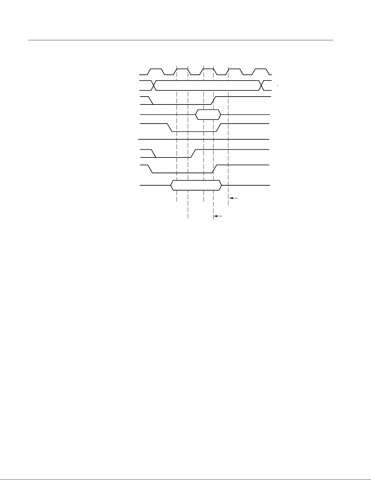
Setting Up the Support
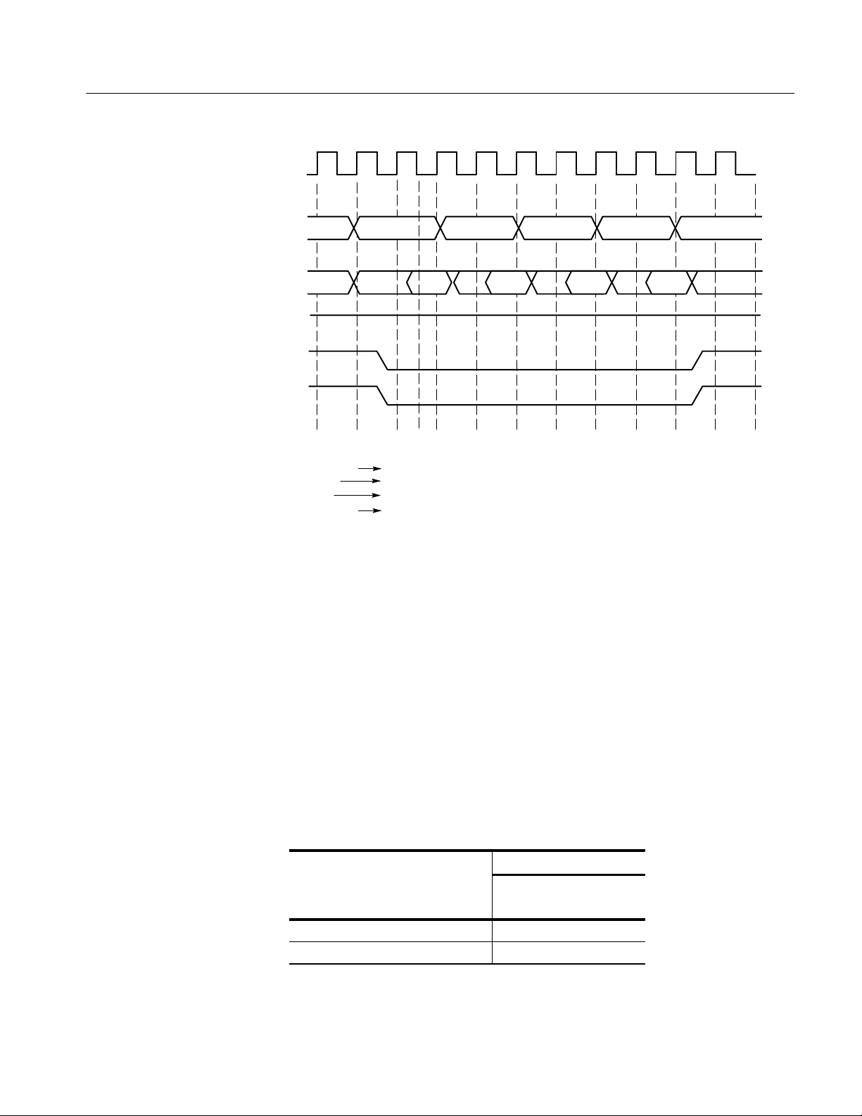
CLK
AC
ADDRESS
DATA
DATA
D
For Non zero Read cycle
For Non zero Read cycle
For Write cycle only
For Write cycle only
Master (for read cycle)
Master (for write cycle)
D
A[22:0]
RE*
D[15:0]
CSx*
ZERO*
DTACK*
WE*
D[15:0]
AC
Figure 2–1: MCF5204 Read/Write bus timing with external terminination and one
wait state
2–4
TMS 221 MCF5204 Microprocessor Support Instruction Manual
Page 41
CLKOUT
Setting Up the Support
Symbols
ADDR [22:0]
DATA [15:0]
ZERO~
RE*
CSx~
ADDR0 ADDR1 ADDR1 ADDR1
D0
AC
D ADCMaster Master ADC Master ADC Master
Note : ZERO~ This signal is derived on probe adapter, See section 5.0 for details.
AC Address/Control done in data phase
D Data done in data phase
Master Master done in final phase
D1 D2 D3
Figure 2–2: MCF5204 Burst cycle bus timing with one wait state
The TMS 221 support supplies symbol table files. Each file replaces specific
channel group values with symbolic values when Symbolic is the radix for the
channel group.
Symbol tables are generally not for use in timing or MCF5204_T support
disassembly.
Table 2–1 lists the name and bit pattern for the symbols in the file 5204_Ctrl, the
Control channel group symbol table.
T able 2–1: Control group symbol table definitions
Control group value
RESET*
Symbol
RESET CYCLE
READ/FETCH
WE*
RE*
011
110
TMS 221 MCF5204 Microprocessor Support Instruction Manual
2–5
Page 42

Setting Up the Support
T able 2–1: Control group symbol table definitions (cont.)
Control group value
RESET*
Symbol
WE*
RE*
DA TA_WRITE
INV ALID
101
111
Table 2–2 lists the name and bit pattern for the symbols in the file 5204_CS, the
Chip Select channel group symbol table.
T able 2–2: Chip Select group symbol table definitions
Control group value
CS3*
CS2*
Symbol
CHIP SELECT–5 REGION
CHIP SELECT–4 REGION
CHIP SELECT–3 REGION
CHIP SELECT–2 REGION
CHIP SELECT–1 REGION
CHIP SELECT–0 REGION
INV ALID CHIP SELECT REGION
CS5* CS1*
CS4* CS0*
0X XXXX
10 XXXX
11 0XXX
11 10XX
11 110X
11 1110
11 1111
2–6
Information on basic operations describes how to use symbolic values for
triggering and for displaying other channel groups symbolically, such as the
Address channel group.
TMS 221 MCF5204 Microprocessor Support Instruction Manual
Page 43

Acquiring And Viewing Disassembled Data
Acquiring Data
Once you load the MCF5204 support, choose a clocking mode, and specify the
trigger, you are ready to acquire and disassemble
If you have any problems acquiring data, refer to information on basic operations
in your online help or Appendix A: Error Messages and Disassembly Pr oblems in
the basic operations user manual.
Viewing Disassembled Data
You can view disassembled data in four display formats: Hardware, Software,
Control Flow, and Subroutine. The information on basic operations describes
how to select the disassembly display formats.
NOTE. Selections in the Disassembly property page (the Disassembly Format
Definition overlay) must be set correctly for your acquired data to be disassembled correctly. Refer to Changing How Data is Displayed on page 2–10.
data.
The default display format shows the Address, Data, and Control channel group
values for each sample of acquired data.
The disassembler displays special characters and strings in the instruction
mnemonics to indicate significant events. Table 2–3 shows these special
characters and strings, and gives a description of what they represent.
T able 2–3: Meaning of special characters in the display
Character or string displayed Description
>> On the TLA 700
m On the DAS 9200
**** Indicates there is insufficient data available for complete
# Indicates an immediate value
t Indicates the number shown is in decimal, such as #12t
The instruction was manually marked as a program fetch
disassembly of the instruction: the number of asterisks
indicates the width of the data that is unavailable. Each two
asterisks represent one byte.
TMS 221 MCF5204 Microprocessor Support Instruction Manual
2–7
Page 44

Acquiring and Viewing Disassembled Data
Hardware Display Format
In Hardware display format, the disassembler displays certain cycle type labels in
parentheses. Table 2–4 shows these cycle type labels and gives a definition of the
cycle they represent. Reads to interrupt and exception vectors will be labeled
with the vector name.
T able 2–4: Cycle type definitions
Cycle type Definition
( DATA READ ) Read cycle
( DATA WRITE ) Write cycle
( UNKNOWN ) The combination of control bits is unexpected and/or
( RESET STATE ) If RESET* signal is low it indicates a RESET state
( ALL CHIP SELECTS DISABLED ) This will be displayed if all chip select regions are high
( CACHE BURST FILL ) w
( EXTENSION ) w
( FLUSH ) w
w Computed cycle types.
unrecognized
example: CS5*–CS0* = 111111
Data burst fill to cache
This cycle is an extension to a preceding instruction cycle
The cycle was fetched but not executed
2–8
TMS 221 MCF5204 Microprocessor Support Instruction Manual
Page 45

Acquiring and Viewing Disassembled Data
Figure 2–3 shows an example of the Hardware display.
1 2 3 4
Sample Address Data Mnemonic
-------------------------------------------------------------------------------108 00040132 44FC MOVE.W #001F,CCR >
109 00040134 001F ( EXTENSION ) >
110 00040136 642A BCC.B 00040162 >
111 00040138 44FC MOVE.W #0000,CCR >
112 0004013A 0000 ( EXTENSION ) >
113 0004013C 6524 BCS.B 00040162 >
114 0004013E 6722 BEQ.B 00040162 >
115 00040140 44FC MOVE.W #0003,CCR >
116 00040142 0003 ( EXTENSION ) >
117 00040144 6C1C BGE.B 00040162 >
118 00040146 6E1A BGT.B 00040162 >
119 00040148 6218 BHI.B 00040162 >
120 0004014A 44FC MOVE.W #0000,CCR >
121 0004014C 0000 ( EXTENSION ) >
122 0004014E 6F12 BLE.B 00040162 >
123 00040150 6310 BLS.B 00040162 >
124 00040152 6D0E BLT.B 00040162 >
125 00040154 6B0C BMI.B 00040162 >
126 00040156 44FC MOVE.W #001F,CCR >
127 00040158 001F ( EXTENSION ) >
128 0004015A 6606 BNE.B 00040162 >
129 0004015C 6A04 BPL.B 00040162 >
130 0004015E 6802 BVC.B 00040162 >
Software Display Format
Control Flow Display
Format
Figure 2–3: Hardware display format
1
Sample Column. Lists the memory locations for the acquired data.
2
Address Group. Lists data from channels connected to the MCF5204
address bus.
3
Data Group. Lists data from channels connected to the MCF5204 data bus.
4
Mnemonics Column. Lists the disassembled instructions and cycle types.
The Software display format shows only the first fetch of executed instructions.
Flushed cycles and extensions are not shown, even though they are part of the
executed instruction. Read extensions will be used to disassemble the instruction,
but will not be displayed as a separate cycle in the Software display format. Data
reads and writes are not displayed.
The Control Flow display format shows only the first fetch of instructions that
change the flow of control, branches are not taken and are not displayed.
TMS 221 MCF5204 Microprocessor Support Instruction Manual
2–9
Page 46

Acquiring and Viewing Disassembled Data
Instructions that unconditionally generate a change in the flow of control in the
MCF5204 microprocessor are:
BRA JSR STOP
BSR RTE TRAP
JMP RTS HALT
Instructions that conditionally generate a change in the flow of control in the
MCF5204 microprocessor are:
Bcc
Subroutine Display
Format
Signals On The Probe
Adapter But Not Acquired
The Subroutine display format shows only the first fetch of subroutine call and
return instructions. It will display conditional subroutine calls if they are
considered to be taken.
Instructions that unconditionally generate a subroutine call or a return in the
MCF5204 microprocessor are:
BSR RTE STOP HALT
JSR RTS TRAP
The following signals are present on the probe adapter, but not acquired by the
disassembler software:
TCLK HIZ/PST0 MTMOD3
If you would like to view these signals, an alternate probing method must be
used.
Changing How Data is Displayed
There are common fields and features that allow you to further modify displayed
data to suit your needs. You can make common and optional display selections in
the Disassembly property page (the Disassembly Format Definition overlay).
2–10
You can make selections unique to the MCF5204 support to do the following
tasks:
H Change how data is displayed across all display formats
H Change the interpretation of disassembled cycles
H Display exception vectors
TMS 221 MCF5204 Microprocessor Support Instruction Manual
Page 47

Acquiring and Viewing Disassembled Data
Optional Display
Selections
You can make optional selections for disassembled data. In addition to the
common selections (described in the information on basic operations), you can
change the displayed data in the following ways.
The MCF5204 microprocessor support product has these additional fields:
Vector Base Register. You can specify the starting address of the vector base
register in hexadecimal. The default starting address is 0x00000000.
CS5* Base Address. Enter the base address of chip select region 5 in this 32-bit
field. The default value is 0x00000000.
CS4* Base Address. Enter the base address of chip select region 4 in this 32-bit
field. The default value is 0x00000000.
CS3* Base Address. Enter the base address of chip select region 3 in this 32-bit
field. The default value is 0x00000000.
CS2* Base Address. Enter the base address of chip select region 2 in this 32-bit
field. The default value is 0x00000000.
CS1* Base Address. Enter the base address of chip select region 1 in this 32-bit
field. The default value is 0x00000000.
CS0* Base Address. Enter the base address of chip select region 0 in this 32-bit
field. The default value is 0x00000000.
Burst Mode (CS5*–CS0*). The burst configuration of the chip select regions are
selected from the list provided. The list box consists of all of the possible burst
configurations. Each selection is made up of a 6-character string composed of
“B’s” for burst mode, and “N’s” for Non-burst mode. The most significant bit
signifies the status of chip select region 5, while the least significant bit signifies
the status of chip select region 0, as shown in Examples 2-1 through 2-3.
B Burst mode
N Non-burst mode
Default value: NNNNNN
Example 2-1:
BNBNNB
Chip select regions: 5, 3, and 0, are burst mode
Chip select regions: 4, 2, and 1, are non-burst mode
TMS 221 MCF5204 Microprocessor Support Instruction Manual
2–11
Page 48

Acquiring and Viewing Disassembled Data
Example 2-2:
BBBBBB
Example 2-3:
NNNNNN
Port Size. The port size configuration is selected from the list provided. The list
box consists of all the possible burst configurations. Each selection is made up of
a 6-character string composed of “B’s” for byte, and “W’s” for word. Byte is a
8-bit port, while word is 16-bit, as shown in Examples 2-4 through 2-6.
B 8-bit byte size port
W 16-bit word size port
Default value: WWWWWW
Chip select regions: 5, 4, 3, 2, 1, and 0, are burst mode
Chip select regions: 5, 4, 3, 2, 1, and 0, are non-burst mode
Example 2-4:
BWWWBW
Region 5, and 1, are 8-bit byte size, and the rest are
16-bit word size.
Example 2-5:
WBWBWB
Regions 5, 3, and 1, are 16-bit word size
Regions 4, 2, and 0, are 8-bit byte size
Example 2-6:
WWWWWW
All regions are 16-bit word size
NOTE. If overlapping address ranges are programmed into the chip select
registers, only one chip select will be asserted. The chip select registers are
prioritized from CS5* to CS0*, with CS5* receiving the highest priority.
This convention is different from previous Motorola products.
2–12
Marking Cycles
The disassembler has a Mark Opcode function that allows you to change the
interpretation of a cycle type. Using this function, you can select a cycle and
change it to one of the following cycle types:
TMS 221 MCF5204 Microprocessor Support Instruction Manual
Page 49

Acquiring and Viewing Disassembled Data
H Opcode – The first word of an instruction
H Extension – A subsequent word of an instruction
H Flush – An opcode or extension that is fetched but not executed
H Data Read – Mark cycle as a Data Read cycle
H Undo Mark – Remove all marks from the current sequence
Displaying Exception
Vectors
The disassembler can display exception vectors.
You can relocate the table by entering the starting address in the Vector Base
Register field. The Vector Base Register field provides the disassembler with the
offset address. Enter an eight-digit hexadecimal value corresponding to the offset
of the base address of the exception table. The Vector Table Size field lets you
specify a three-digit hexadecimal size for the table.
These fields are located in the Disassembly property page (Disassembly Format
Definition overlay).
Table 2–5 lists the MCF5204 exception vectors.
T able 2–5: Exception vectors
Exception
number
0 000 ( INITIAL STACK POINTER )
1 004 ( INITIAL PROGRAM COUNTER )
2 008 ( ACCESS ERROR VECTOR )
3 00C ( ADDRESS ERROR VECTOR )
4 010 ( ILLEGAL INSTRUCTION VECTOR )
5 014 ( RESERVED VECTOR #14H )
6 018 ( RESERVED VECTOR #18H )
7 01C ( RESERVED VECTOR #1CH )
8 020 ( PRIV VIOLATION VECTOR )
9 024 ( TRACE VECTOR )
10 028 ( UNIMPLEMENTED LINE-A OPCODE )
11 02C ( UNIMPLEMENTED LINE-F OPCODE )
12 030 ( DEBUG INTERRUPT VECTOR )
13 034 ( RESERVED VECTOR #34H )
14 038 ( FORMAT ERROR VECTOR )
15 03C ( UNINIT INTERRUPT VECTOR )
16-23 040-05C ( RESERVED VECTOR #40H #5CH )
Location in table
(in hexadecimal)
Displayed exception name
TMS 221 MCF5204 Microprocessor Support Instruction Manual
2–13
Page 50
Acquiring and Viewing Disassembled Data
T able 2–5: Exception vectors (cont.)
Exception
number
24 060 ( SPURIOUS INTERRUPT VECTOR )
25-31 064-07C ( ILP 1-7 AUTOVECTOR )
32-47 080-08C ( TRAP #0t-#15t VECTOR )
48-63 0C0-0FC ( RESERVED VECTOR #C0-#FC )
64-255 100-3FC ( USER INT VECTOR #64t-#255t )
Location in table
(in hexadecimal)
Displayed exception name
2–14
TMS 221 MCF5204 Microprocessor Support Instruction Manual
Page 51

Specifications
Page 52

Page 53

Specifications
Specification Tables
These specifications are for a probe adapter connected between a compatible
Tektronix logic analyzer and a SUT. Table 3–1 shows the electrical requirements
the SUT must produce for the support to acquire correct data. Table 3–2 shows
the environmental specifications.
Figure 3–1 shows the dimensions of the probe adapter. Figure 3–2 shows the
dimensions of the test clip.
T able 3–1: Electrical specifications
Characteristics Requirements
SUT DC power requirements
Voltage 4.75–5.25 VDC
Current I
SUT clock rate
Maximum specified clock rate 33 MHz
Tested clock rate 25 MHz
Minimum setup time required
TLA 700 2.5 ns
DAS 9200 5 ns
Minimum hold time required
TLA 700 0 ns
DAS 9200 0 ns
Typical signal loading
TLA 700 MICTOR load (ML) w 20 KW in parallel with 2 pF
TLA 700 podlet load (CL) w 20 KW in parallel with 2 pF
DAS 9200 MICTOR load (ML)
DAS 9200 podlet load (CL)
Characteristics Specification
Measured typical SUT signal loading AC load DC load
UWE*/UDS*, LWE*/LDS*, TIN/PP2,
TOUT/PP3
max
I
typ
100 KW in parallel with 12 pF
100 KW in parallel with 10 pF
14 pF + 1 ML w
131.5 mA
87 mA
1 ML
PST0, PST1, PST2, PST3 20 pF + 1 ML 1 ML
DDA TA0, DDATA1, DDATA2, DDATA3
TMS 221 MCF5204 Microprocessor Support Instruction Manual
20 pF + 1 CL w
1 ML + 1 CL
3–1
Page 54

Specifications
T able 3–1: Electrical specifications (cont.)
Characteristics Requirements
CLK 24 pF + 1 ML 1 ML
A[1–0] 10 pF + 2 ML 2 ML
CS0*, CS1*, CS2*, CS3*, CS4*, CS5* 20 pF + 1 ML 1 ML + 1 20V8 PAL
A[21–2] 10 pF + 1 ML 1 ML
D[15–0] 8 pF + 1 ML 1 ML
IRQ[3–0]* 14 pF + 1 ML 1 ML
RESET* 13 pF + 1 ML 1 ML
RE*, WE*, CTS*/PP6, RXD/PP5, 10 pF + 1 ML 1 ML
DTACK*, TXD/PP4 5 pF + 1 ML 1 ML
ATS*, RTS*/PP7, 15 pF + 1 ML 1 ML
BKPT*/TMS 24 pF + 1 ML 1 ML
DSO/TDO, DSI/TDI, DSCLK/TRST,
TCLK, MTMOD
20 pF + 1 ML 1 ML
w ML is Mictor load, CL is clock load.
3–2
TMS 221 MCF5204 Microprocessor Support Instruction Manual
Page 55
T able 3–2: Environmental specifications*
Characteristic Description
Temperature
Specifications
Maximum operating
Minimum operating 0° C (+32° F)
Non-operating –55° C to +75° C (–67° to +167° F)
Humidity 10 to 95% relative humidity
Altitude
Operating 4.5 km (15,000 ft) maximum
Non-operating 15 km (50,000 ft) maximum
Electrostatic immunity The probe adapter is static sensitive
* Designed to meet Tektronix standard 062-2847-00 class 5.
[
Not to exceed MCF5204 microprocessor thermal considerations. Forced air cooling
might be required across the CPU.
+50° C (+122° F)[
TMS 221 MCF5204 Microprocessor Support Instruction Manual
3–3
Page 56
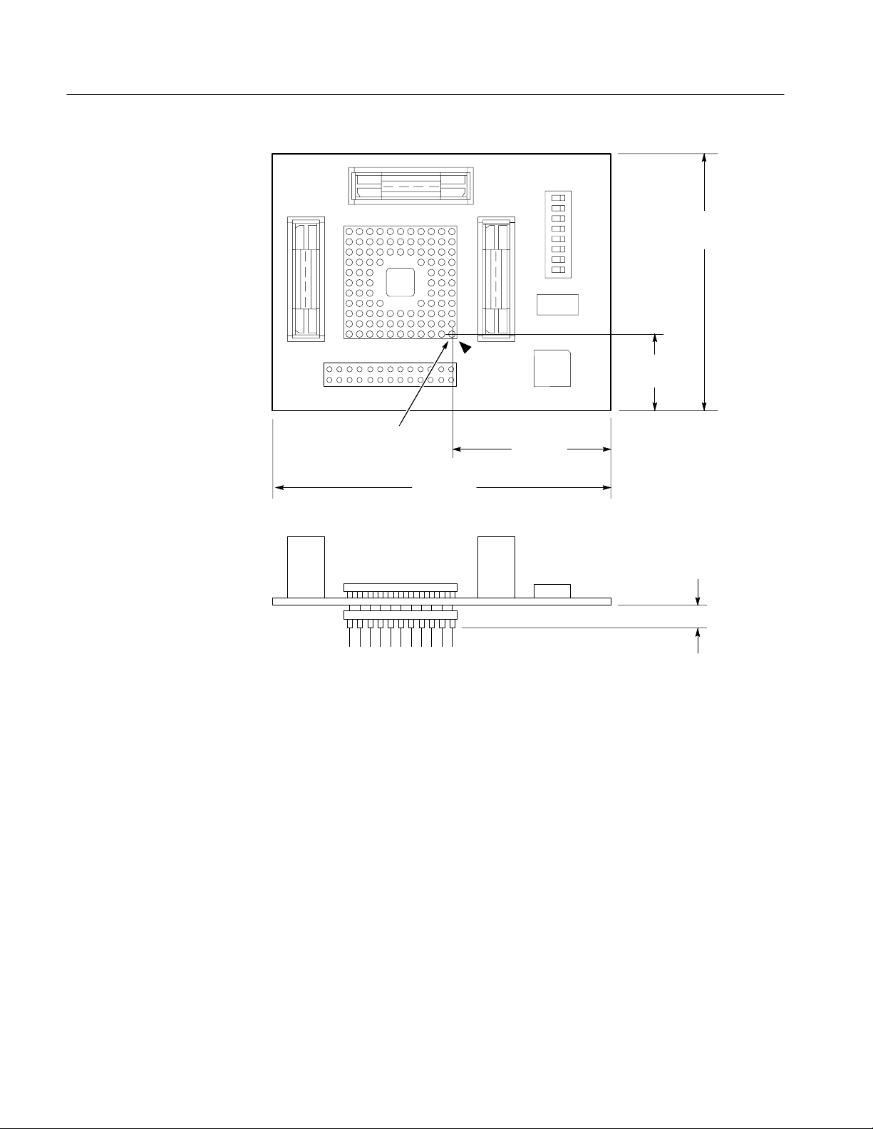
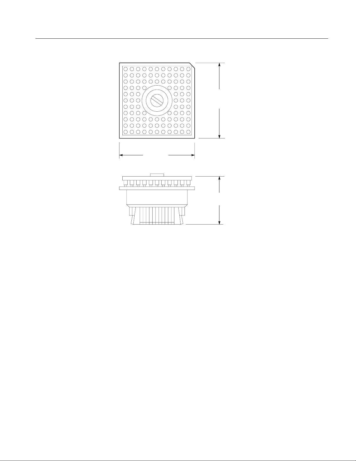
Specifications
66 mm
(2.600 in)
19 mm
(.750 in)
Pin 1
76 mm
(3.300 in)
38 mm
(1.500 in)
Figure 3–1: Dimensions of the probe adapter
7. mm (.26 in)
3–4
TMS 221 MCF5204 Microprocessor Support Instruction Manual
Page 57
29 mm
(1.150 in)
Specifications
29 mm
(1.150 in)
19 mm
(.765 in)
Figure 3–2: Dimensions of the test clip
TMS 221 MCF5204 Microprocessor Support Instruction Manual
3–5
Page 58

Specifications
3–6
TMS 221 MCF5204 Microprocessor Support Instruction Manual
Page 59

WARNING
The following servicing instructions are for use only by qualified personnel. To
avoid injury, do not perform any servicing other than that stated in the operating
instructions unless you are qualified to do so. Refer to all Safety Summaries
before performing any service.
Page 60

Page 61

Maintenance
Page 62

Page 63

Maintenance
Probe Adapter Description
The probe adapter is nonintrusive hardware that allows the logic analyzer to
acquire data from a microprocessor in its own operating environment with little
or no effect on that system. Information on basic operations contains a figure
showing the logic analyzer connected to a typical probe adapter. Refer to that
figure while reading the following description.
The probe adapter consists of a circuit board and a socket for a MCF5204
microprocessor. The probe adapter connects to the microprocessor in the SUT.
Signals from the microprocessor-based system flow from the probe adapter to the
channel groups and through the probe signal leads to the module.
The probe adapter accommodates the Motorola MCF5204 microprocessor in a
100-pin TQFP package.
In the MCF5204 there is no external signal on the bus to indicate a Zero Wait
State cycle. A signal ZERO* is derived on the probe adapter with the help of
CS[5-0]* signals, and used as a qualifier. This signal is valid when any one of the
memory region is configured for ZERO Wait state operation.
Replacing Signal Leads
The address space of the MCF5204 must be configured in any one of the six
possible chip select signals CS[5-0]*. All these signals are logically ORed with a
PAL chip. Use the DIP switch on the probe adapter to select the particular chip
select for the memory region that is configured for Zero Wait state.
Information on basic operations describes how to replace signal leads (individual
channel and clock probes).
TMS 221 MCF5204 Microprocessor Support Instruction Manual
4–1
Page 64

Maintenance
4–2
TMS 221 MCF5204 Microprocessor Support Instruction Manual
Page 65

Replaceable Electrical Parts
Page 66

Page 67

Replaceable Electrical Parts
This chapter contains a list of the replaceable electrical components for the
TMS 221 MCF5204 microprocessor support. Use this list to identify and order
replacement parts.
Parts Ordering Information
Replacement parts are available through your local Tektronix field office or
representative.
Changes to Tektronix products are sometimes made to accommodate improved
components as they become available and to give you the benefit of the latest
improvements. Therefore, when ordering parts, it is important to include the
following information in your order:
H Part number
H Instrument type or model number
H Instrument serial number
H Instrument modification number, if applicable
If you order a part that has been replaced with a different or improved part, your
local Tektronix field office or representative will contact you concerning any
change in part number.
Change information, if any, is located at the rear of this manual.
Using the Replaceable Electrical Parts List
The tabular information in the Replaceable Electrical Parts List is arranged for
quick retrieval. Understanding the structure and features of the list will help you
find all of the information you need for ordering replacement parts. The
following table describes each column of the electrical parts list.
TMS 221 MCF5204 Microprocessor Support Instruction Manual
5–1
Page 68
Replaceable Electrical Parts
Parts list column descriptions
Column Column name Description
1 Component number The component number appears on diagrams and circuit board illustrations, located in the diagrams
section. Assembly numbers are clearly marked on each diagram and circuit board illustration in the
Diagrams section, and on the mechanical exploded views in the Replaceable Mechanical Parts list
section. The component number is obtained by adding the assembly number prefix to the circuit
number (see Component Number illustration following this table).
The electrical parts list is arranged by assemblies in numerical sequence (A1, with its subassemblies
and parts, precedes A2, with its subassemblies and parts).
Chassis-mounted parts have no assembly number prefix, and they are located at the end of the
electrical parts list.
2 Tektronix part number Use this part number when ordering replacement parts from Tektronix.
3 and 4 Serial number Column three indicates the serial number at which the part was first effective. Column four indicates
the serial number at which the part was discontinued. No entry indicates the part is good for all serial
numbers.
5 Name & description An item name is separated from the description by a colon (:). Because of space limitations, an item
name may sometimes appear as incomplete. Use the U.S. Federal Catalog handbook H6-1 for
further item name identification.
6 Mfr. code This indicates the code number of the actual manufacturer of the part.
7 Mfr. part number This indicates the actual manufacturer’s or vendor’s part number.
Abbreviations
Component Number
List of Assemblies
Chassis Parts
Mfr. Code to Manufacturer
Cross Index
Abbreviations conform to American National Standard ANSI Y1.1–1972.
Component number
A23A2R1234 A23 R1234
Assembly number Circuit number
Read: Resistor 1234 (of Subassembly 2) of Assembly 23
A2
Subassembly number
(optional)
A list of assemblies is located at the beginning of the electrical parts list. The
assemblies are listed in numerical order. When a part’s complete component
number is known, this list will identify the assembly in which the part is located.
Chassis-mounted parts and cable assemblies are located at the end of the
Replaceable Electrical Parts List.
The table titled Manufacturers Cross Index shows codes, names, and addresses of
manufacturers or vendors of components listed in the parts list.
5–2
TMS 221 MCF5204 Microprocessor Support Instruction Manual
Page 69

Replaceable Electrical Parts
Manufacturers cross index
Mfr.
code
00779 AMP INC. CUSTOMER SERVICE DEPT
05276 ITT POMONA ELECTRONICS 1500 E NINTH ST POMONA, CA 91766–3835
09353 C & K COMPONENTS CORP 15 RIVERDALE AVENUE NEWTON, MA 02158
60381 PRECISION INTERCONNECT CORP. 16640 SW 72ND AVE PORTLAND, OR 97224
63058 BERG ELECTRONICS INC. MCKENZIE SOCKET DIV
80009 TEKTRONIX INC 14150 SW KARL BRAUN DR
Manufacturer Address City , state, zip code
PO BOX 3608
910 PAGE AVE
PO BOX 500
HARRISBURG, PA 17105–3608
FREMONT , CA 94538–7340
BEAVERT ON, OR 97077–0001
Replaceable electrical parts list
Component
number
– 105–1089–00 LATCH ASSY:LATCH HOUSING ASSY,VERTICAL
– 131–5267–00 CONN,HDR:PCB,MALE,STR,2 X 40,0.1 CTR,0.235 MLG
– 131–6134–01 CONN,RCPT:SMD,MICTOR,PCB,STR,38
– 136–1317–00 SOCKET ,PGA:PCB,FEMALE,STR,100 POS,1 1 X 11,0.1
– 260–5000–00 SWITCH,SLIDE:SPST,DIP8 POSITION,GOLD OVER
– 389–2489–00 CICRUIT BOARD:TQFP–100,SOLDERED,TMS221 OPT
– 671–4253–00 CKT BRD
Tektronix
part number
Serial no.
effective
Serial no.
discont’d
Name & description Mfr. code Mfr. part number
MOUNT,0.48 H X 1.24 L,W/PCB SINGLE CLIP,P6434
X 0.110 T AIL,30GOLD, HIGH TEMP,
POS,FEMALE,0.025 CTR,0.240 H,W/0.108 PCB HOLD
DOWNS.PALLAD
CTR,0.0.173 H X 0.273 TAIL,G/G,OPEN CENTER,L
NICKEL,3A,2PF ,SEALED,90HBW08S,44MM T&R
11,
ASSY:MCF5204,TQFP–100,SOLDERED,679–4253–00
TESTED,389–2489–00 WIRED,TMS221 11
60381 105–1089–00
00779 104326–4
00779 767054–1
63058 PGA100H115B1–1149
F
09353 LD08HOSK1
01KV9 389–2489–00
80009 671–4253–00
TMS 221 MCF5204 Microprocessor Support Instruction Manual
5–3
Page 70

Replaceable Electrical Parts
5–4
TMS 221 MCF5204 Microprocessor Support Instruction Manual
Page 71
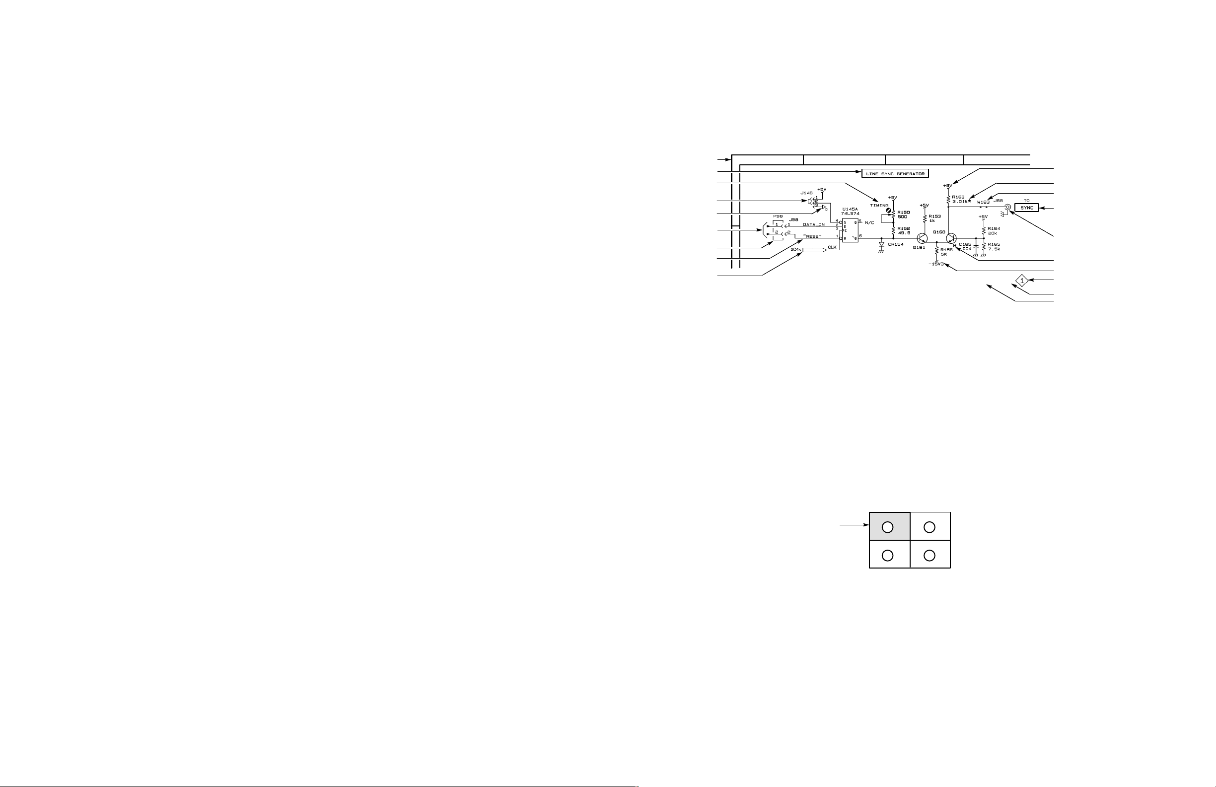
Diagrams and Circuit Board Illustrations
diagram, and corresponding component locator illustration. The Replaceable Electrical
Parts list is arranged by assembly in numerical sequence; the components are listed by
component number.
Symbols
Component Values
This section contains the troubleshooting procedures, block diagrams, circuit board
illustrations, component locator tables, waveform illustrations, and schematic diagrams.
Graphic symbols and class designation letters are based on ANSI Standard Y32.2-1975.
Abbreviations are based on ANSI Y1.1-1972.
Logic symbology is based on ANSI/IEEE Standard 91-1984 in terms of positive logic.
Logic symbols depict the logic function performed and can differ from the manufacturer’s
data.
The tilde (~) preceding a signal name indicates that the signal performs its intended
function when in the low state.
Other standards used in the preparation of diagrams by Tektronix, Inc., include the
following:
H Tektronix Standard 062-2476 Symbols and Practices for Schematic Drafting
H ANSI Y14.159-1971 Interconnection Diagrams
H ANSI Y32.16-1975 Reference Designations for Electronic Equipment
H MIL-HDBK-63038-1A Military Standard Technical Manual Writing Handbook
Locator Grid
Function Block Title
Internal Screw Adjustment
Onboard Jumper
Digital Ground
Refer to Assembly
& Diagram Number
Offboard Connector
Active Low Signal
Signal From
Another Diagram,
Same Board
A
B
12 3 4
Component Locator Diagrams
The schematic diagram and circuit board component location illustrations have grids
marked on them. The component lookup tables refer to these grids to help you locate a
component. The circuit board illustration appears only once; its lookup table lists the
diagram number of all diagrams on which the circuitry appears.
Some of the circuit board component location illustrations are expanded and divided into
several parts to make it easier for you to locate small components. To determine which
part of the whole locator diagram you are looking at, refer to the small locator key shown
below. The gray block, within the larger circuit board outline, shows where that part fits
in the whole locator diagram. Each part in the key is labeled with an identifying letter that
appears in the figure titles under component locator diagrams.
Power Termination
Component on back of board
Strap
Panel Control
Female Coaxial
Connector
Heat Sink
Decoupled Voltage
Diagram Number
Assembly Number
Diagram Name
Electrical components shown on the diagrams are in the following units unless noted
otherwise:
Capacitors: Values one or greater are in picofarads (pF).
Values less than one are in microfarads (mF).
Resistors: Values are in Ohms (W).
Graphic Items and Special Symbols Used in This Manual
Each assembly in the instrument is assigned an assembly number (for example A5). The
assembly number appears in the title on the diagram, in the lookup table for the schematic
TMS 221 MCF5204 Microprocessor Support Instruction Manual
Section of Circuit
Board Shown
A B
DC
5–5
Page 72

R100
C120
J310
S100
U100
J200
U200
J600
J500
5–6
TMS 221 MCF5204 Microprocessor Support Instruction Manual
Page 73
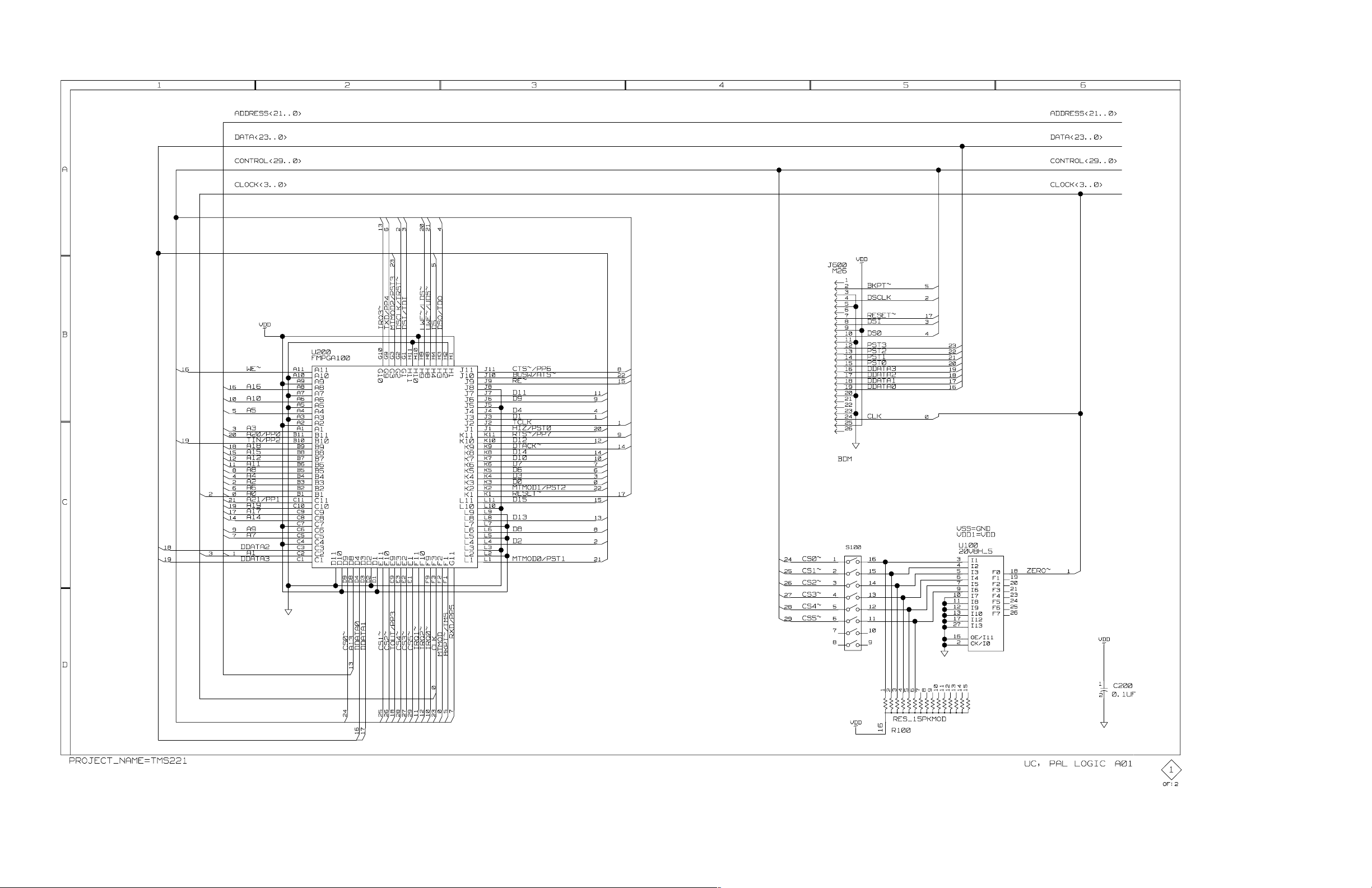
Page 74

Page 75

Page 76

Page 77

Replaceable Mechanical Parts
Page 78

Page 79

Replaceable Mechanical Parts
This chapter contains a list of the replaceable mechanical components for the
TMS 221 MCF5204 microprocessor support. Use this list to identify and order
replacement parts.
Parts Ordering Information
Replacement parts are available through your local Tektronix field office or
representative.
Changes to Tektronix products are sometimes made to accommodate improved
components as they become available and to give you the benefit of the latest
improvements. Therefore, when ordering parts, it is important to include the
following information in your order:
H Part number
H Instrument type or model number
H Instrument serial number
H Instrument modification number, if applicable
If you order a part that has been replaced with a different or improved part, your
local Tektronix field office or representative will contact you concerning any
change in part number.
Change information, if any, is located at the rear of this manual.
Using the Replaceable Mechanical Parts List
The tabular information in the Replaceable Mechanical Parts List is arranged for
quick retrieval. Understanding the structure and features of the list will help you
find all of the information you need for ordering replacement parts. The
following table describes the content of each column in the parts list.
TMS 221 MCF5204 Microprocessor Support Instruction Manual
6–1
Page 80

Replaceable Mechanical Parts
Parts list column descriptions
Column Column name Description
1 Figure & index number Items in this section are referenced by figure and index numbers to the exploded view illustrations
that follow.
2 Tektronix part number Use this part number when ordering replacement parts from Tektronix.
3 and 4 Serial number Column three indicates the serial number at which the part was first effective. Column four
indicates the serial number at which the part was discontinued. No entries indicates the part is
good for all serial numbers.
5 Qty This indicates the quantity of parts used.
6 Name & description An item name is separated from the description by a colon (:). Because of space limitations, an
item name may sometimes appear as incomplete. Use the U.S. Federal Catalog handbook H6-1
for further item name identification.
7 Mfr. code This indicates the code of the actual manufacturer of the part.
8 Mfr. part number This indicates the actual manufacturer’s or vendor’s part number.
Abbreviations
Chassis Parts
Mfr. Code to Manufacturer
Cross Index
Abbreviations conform to American National Standard ANSI Y1.1–1972.
Chassis-mounted parts and cable assemblies are located at the end of the
Replaceable Electrical Parts List.
The table titled Manufacturers Cross Index shows codes, names, and addresses of
manufacturers or vendors of components listed in the parts list.
6–2
TMS 221 MCF5204 Microprocessor Support Instruction Manual
Page 81

Replaceable Mechanical Parts
Manufacturers cross index
Mfr.
code
00779 AMP INC. CUSTOMER SERVICE DEPT
05276 ITT POMONA ELECTRONICS 1500 E NINTH ST POMONA, CA 91766–3835
09353 C & K COMPONENTS CORP 15 RIVERDALE AVENUE NEWTON, MA 02158
60381 PRECISION INTERCONNECT CORP. 16640 SW 72ND AVE PORTLAND, OR 97224
63058 BERG ELECTRONICS INC. MCKENZIE SOCKET DIV
80009 TEKTRONIX INC 14150 SW KARL BRAUN DR
Manufacturer Address City , state, zip code
PO BOX 3608
910 PAGE AVE
PO BOX 500
HARRISBURG, PA 17105–3608
FREMONT , CA 94538–7340
BEAVERT ON, OR 97077–0001
Replaceable parts list
Fig. &
index
number
1–0 010–0615–00 1 ADAPTER, PROBE: MCF5204, TQFP–100
–1 671–4253–00 1 CKT BRD ASSY: MCF5204, TQFP–100, SOLDERED,
–2 131–6134–01 3 CONN, RCPT: SMD, MICTOR, PCB, STR, 38 POS,
–3 105–1089–00 3 LATCH ASSY: LATCH HOUSING ASSY, VERTICAL
–4 260–5000–00 1 SWITCH, SLIDE: SPST , DIP8 POSITION, GOLD OVER
–5 131–5267–00 1 CONN, HDR: PCB, MALE, STR, 2 X 40,0.1 CTR, 0.235
–6 103–041 1–00 1 ADAPTER, TQFP: TEST CLIP, 100 PIN TQFP, 0.50
–7 136–1317–00 1 SOCKET, PGA: PCB, FEMALE, STR, 100 POS, 11 X
Tektronix
part number
070–9803–00 1 MANUAL, TECH: INSTRUCTION,
071–0042–00 1 MANUAL, TECH: INSTRUCTION, MCF5204, TMS221 TK2548 071–0042–00
070–9802–00 1 MANUAL, TECH: BASIC OPS MICRO SUP ON
Serial no.
effective
Serial no.
discont’d
Qty Name & description Mfr. code Mfr. part number
SOLDERED, TMS221 OPT 11
679–4253–00 TESTED, 389–2489–00 WIRED,
TMS221 11
FEMALE, 0.025 CTR, 0.240 H, W/0.108 PCB HOLD
DOWNS. PALLAD
MOUNT, 0.48 H X 1.24 L, W/PCB SINGLE CLIP, P6434
NICKEL, 3A, 2PF , SEALED
MLG X 0.110 TAIL, 30GOLD, HIGH TEMP
MM LEAD PITCH, MCF5202/03, 100 POS
11, 0.1 CTR, 0.0.173 H X 0.273 TAIL, G/G, OPEN
CENTER
MICROPROCESSOR SUPPORT , PKG
INSTALLATION, TLA700 SERIES, LOGIC ANAL YZER
OPTIONAL ACCESSORIES
DAS/TLA 500 SERIES LOGIC ANALYZERS
80009 010–0615–00
80009 671–4253–00
00779 767054–1
60381 105–1089–00
09353 LD08HOSK1
00779 104326–4
05276 MODEL 6150
63058 PGA100H115B1–1149
F
TK2548 070–9803–00
80009 070–9802–00
TMS 221 MCF5204 Microprocessor Support Instruction Manual
6–3
Page 82
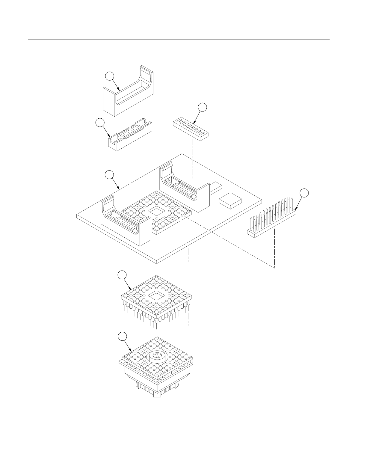
Replaceable Mechanical Parts
2
3
4
1
5
7
6
Figure 6–1: MCF5204 probe adapter exploded view
6–4
TMS 221 MCF5204 Microprocessor Support Instruction Manual
Page 83

Index
Page 84

Page 85

Index
Numbers
5204, definition, ix
520X, definition, ix
A
about this manual set, ix
acquiring data, 2–7
Address group
channel assignments, 1–8
display column, 2–9
application, logic analyzer configuration, 1–1
B
background debug mode connector, 1–1 1
basic operations, where to find information, ix
BDM, pinout, 1–11
Big-Endian byte ordering, 1–2
burst mode (CS5*–CS0*) field, 2–11
bus cycles, displayed cycle types, 2–8
byte ordering, 1–2
C
cache invalidation, 1–2
channel assignments
Address group, 1–8
background debug mode, 1–11
chip select group, 1–10
clocks, 1–11
Control group, 1–10
Data group, 1–9
Intr group, 1–10
Misc group, 1–11
channel groups, 2–1
Chip Select, symbol table, 2–6
chip select group, channel assignments, 1–10
clock channel assignments, 1–11
clock rate, 1–2
SUT, 3–1
clocking, Custom, 2–1
component locator diagrams, 5–5
connections
CPU to Mictor, 1–12
P6434 probes, 1–5
probe adapter to SUT, QFP, 1–4
without probe adapter, 1–7
channel probes, 1–7
contacting T ektronix, x
Control Flow display format, 2–9
Control group
channel assignments, 1–10
symbol table, 2–5
CPU to Mictor connections, 1–12
CS0* base address field, 2–11
CS1* base address field, 2–11
CS2* base address field, 2–11
CS3* base address field, 2–11
CS4* base address field, 2–11
CS5* base address field, 2–11
Custom clocking, 2–1
custom clocking, 2–2
EXT_TRN state, 2–3
STAR T state, 2–2
WAIT state, 2–3
WRITE state, 2–3
cycle types, 2–8
D
data
acquiring, 2–7
disassembly formats
Control Flow, 2–9
Hardware, 2–8
Software, 2–9
Subroutine, 2–10
how it is acquired, 2–1
data display , changing, 2–10
Data group
channel assignments, 1–9
display column, 2–9
data reads and writes, 1–2
diagrams and circuit board illustrations, 5–5–5–6
dimensions, probe adapter, 3–4
DIP switch
configuring, 1–2
example, 1–3
settings, 1–2
disassembled data
cycle type definitions, 2–8
viewing, 2–7
disassembler
definition, ix
logic analyzer configuration, 1–1
TMS 221 MCF5204 Microprocessor Support Instruction Manual
Index–1
Page 86

Index
setup, 2–1
Disassembly Format Definition overlay, 2–11
Disassembly property page, 2–11
display formats
Control Flow, 2–9
Hardware, 2–8
Software, 2–9
special characters, 2–7
Subroutine, 2–10
E
electrical specifications, 3–1
clock rate, 3–1
loading, 3–1
electrostatic immunity, 3–3
environmental specifications, 3–3
altitude, 3–3
humidity , 3–3
temperature, 3–3
exception vectors, 2–13
EXT_TRN state, 2–3
H
Hardware display format, 2–8
cycle type definitions, 2–8
hold time, minimum, 3–1
I
information on basic operations, definition, ix
inspection and cleaning
microcontroller, 1–5
QFP test clip, 1–5
Internal cache, 1–2
Intr group, channel assignments, 1–10
L
M
manual
conventions, ix
how to use the set, ix
Mark Cycle function, 2–12
Mark Opcode function, 2–12
marking cycles, definition of, 2–12
Mictor to CPU connections, 1–12
Misc group, channel assignments, 1–11
Mnemonics display column, 2–9
P
P54C, definition, ix
P6434 probes, connecting. See connections
package, TQFP, 1–1
port size field, 2–12
power requirements, SUT , 3–1
probe adapter
chip select switch, 1–2
DIP switch settings, 1–2
example settings, 1–3
circuit description, 4–1
clearance, dimensions, 3–4
configuring the DIP switch, 1–2
example, 1–3
connecting the P6434 probes, 1–5
hardware description, 4–1
how to unlock test clip, 1–7
inspection and cleaning, 1–5
not using one, 1–7
removing, 1–7
Q
QFP test clip, 1–4
attaching to microcontroller, 1–6
attaching to probe adapter, 1–4
inspection and cleaning, 1–5
loading, 3–1
signal, 3–1
logic analyzer
configuration for disassembler, 1–1
configuration for the application, 1–1
with a DAS 9200 series, 1–1
with a TLA 700 series, 1–1
definition, x
software compatibility, 1–1
Index–2
R
reference material, 1–1
Reset, SUT hardware, 1–2
restrictions, 1–1
TMS 221 MCF5204 Microprocessor Support Instruction Manual
Page 87

Index
S
set up time, minimum, 3–1
setups, disassembler, 2–1
signal loading, 3–1
signals, active low sign, x
signals not acquired, 2–10
Software display format, 2–9
special characters displayed, 2–7
specifications, 3–1
channel assignments, 1–8
electrical, 3–1
environmental, 3–3
mechanical (dimensions), 3–4
start state, 2–2
static discharge
caution statment, 1–4
how to disapate, 1–4
Subroutine display format, 2–10
support setup, 2–1
supported package style, 1–1
SUT
definition, x
probe adapter connection procedure, 1–4
SUT hardware Reset, 1–2
symbol table
Chip Select, 2–6
Control channel group, 2–5
system clock rate, 1–2
system under test, definition, x
T
terminology, ix
test clip
connecting to probe adapter, 1–4
how to lock, 1–6
how to unlock, 1–7
inspection and cleaning, 1–5
installing, 1–4
QFP, 1–4
removing, 1–7
TQFP package, 1–1
typical signal loading, 3–1
V
vector base register field, 2–11
viewing disassembled data, 2–7
W
wait state, 2–3
write state, 2–3
X
XXX, definition, ix
TMS 221 MCF5204 Microprocessor Support Instruction Manual
Index–3
Page 88

Index
Index–4
TMS 221 MCF5204 Microprocessor Support Instruction Manual
 Loading...