

Page 1

Instruction Manual
TMS 161
80960Cx Microprocessor Support
070-9816-00
There are no current European directives that
apply to this product. This product provides
cable and test lead connections to a test object of
electronic measuring and test equipment.
Warning
The servicing instructions are for use by
qualified personnel only. To avoid personal
injury, do not perform any servicing unless you
are qualified to do so. Refer to all safety
summaries prior to performing service.
Page 2

Copyright T ektronix, Inc. All rights reserved. Licensed software products are owned by Tektronix or its suppliers and are
protected by United States copyright laws and international treaty provisions.
Use, duplication, or disclosure by the Government is subject to restrictions as set forth in subparagraph (c)(1)(ii) of the
Rights in T echnical Data and Computer Software clause at DFARS 252.227-7013, or subparagraphs (c)(1) and (2) of the
Commercial Computer Software – Restricted Rights clause at F AR 52.227-19, as applicable.
T ektronix products are covered by U.S. and foreign patents, issued and pending. Information in this publication supercedes
that in all previously published material. Specifications and price change privileges reserved.
Printed in the U.S.A.
T ektronix, Inc., P.O. Box 1000, Wilsonville, OR 97070–1000
TEKTRONIX and TEK are registered trademarks of T ektronix, Inc.
Page 3

SOFTWARE WARRANTY
T ektronix warrants that the media on which this software product is furnished and the encoding of the programs on
the media will be free from defects in materials and workmanship for a period of three (3) months from the date of
shipment. If a medium or encoding proves defective during the warranty period, T ektronix will provide a
replacement in exchange for the defective medium. Except as to the media on which this software product is
furnished, this software product is provided “as is” without warranty of any kind, either express or implied.
T ektronix does not warrant that the functions contained in this software product will meet Customer’s
requirements or that the operation of the programs will be uninterrupted or error-free.
In order to obtain service under this warranty, Customer must notify Tektronix of the defect before the expiration
of the warranty period. If T ektronix is unable to provide a replacement that is free from defects in materials and
workmanship within a reasonable time thereafter, Customer may terminate the license for this software product
and return this software product and any associated materials for credit or refund.
THIS WARRANTY IS GIVEN BY TEKTRONIX IN LIEU OF ANY OTHER WARRANTIES, EXPRESS
OR IMPLIED. TEKTRONIX AND ITS VENDORS DISCLAIM ANY IMPLIED WARRANTIES OF
MERCHANTABILITY OR FITNESS FOR A PARTICULAR PURPOSE. TEKTRONIX’
RESPONSIBILITY TO REPLACE DEFECTIVE MEDIA OR REFUND CUSTOMER’S PAYMENT IS
THE SOLE AND EXCLUSIVE REMEDY PROVIDED TO THE CUSTOMER FOR BREACH OF THIS
WARRANTY. TEKTRONIX AND ITS VENDORS WILL NOT BE LIABLE FOR ANY INDIRECT,
SPECIAL, INCIDENTAL, OR CONSEQUENTIAL DAMAGES IRRESPECTIVE OF WHETHER
TEKTRONIX OR THE VENDOR HAS ADVANCE NOTICE OF THE POSSIBILITY OF SUCH
DAMAGES.
Page 4

HARDWARE WARRANTY
T ektronix warrants that the products that it manufactures and sells will be free from defects in materials and
workmanship for a period of one (1) year from the date of shipment. If a product proves defective during this
warranty period, T ektronix, at its option, either will repair the defective product without charge for parts and labor,
or will provide a replacement in exchange for the defective product.
In order to obtain service under this warranty, Customer must notify Tektronix of the defect before the expiration
of the warranty period and make suitable arrangements for the performance of service. Customer shall be
responsible for packaging and shipping the defective product to the service center designated by T ektronix, with
shipping charges prepaid. Tektronix shall pay for the return of the product to Customer if the shipment is to a
location within the country in which the T ektronix service center is located. Customer shall be responsible for
paying all shipping charges, duties, taxes, and any other charges for products returned to any other locations.
This warranty shall not apply to any defect, failure or damage caused by improper use or improper or inadequate
maintenance and care. T ektronix shall not be obligated to furnish service under this warranty a) to repair damage
resulting from attempts by personnel other than T ektronix representatives to install, repair or service the product;
b) to repair damage resulting from improper use or connection to incompatible equipment; c) to repair any
damage or malfunction caused by the use of non-T ektronix supplies; or d) to service a product that has been
modified or integrated with other products when the effect of such modification or integration increases the time
or difficulty of servicing the product.
THIS WARRANTY IS GIVEN BY TEKTRONIX IN LIEU OF ANY OTHER WARRANTIES, EXPRESS
OR IMPLIED. TEKTRONIX AND ITS VENDORS DISCLAIM ANY IMPLIED WARRANTIES OF
MERCHANTABILITY OR FITNESS FOR A PARTICULAR PURPOSE. TEKTRONIX’
RESPONSIBILITY TO REPAIR OR REPLACE DEFECTIVE PRODUCTS IS THE SOLE AND
EXCLUSIVE REMEDY PROVIDED TO THE CUST OMER FOR BREACH OF THIS WARRANTY.
TEKTRONIX AND ITS VENDORS WILL NOT BE LIABLE FOR ANY INDIRECT , SPECIAL,
INCIDENTAL, OR CONSEQUENTIAL DAMAGES IRRESPECTIVE OF WHETHER TEKTRONIX OR
THE VENDOR HAS ADVANCE NOTICE OF THE POSSIBILITY OF SUCH DAMAGES.
Page 5

Table of Contents
Getting Started
Operating Basics
General Safety Summary v. . . . . . . . . . . . . . . . . . . . . . . . . . . . . . . . . . . .
Service Safety Summary vii. . . . . . . . . . . . . . . . . . . . . . . . . . . . . . . . . . . . .
Preface: Microprocessor Support Documentation ix. . . . . . . . . . . . . . . .
Manual Conventions ix. . . . . . . . . . . . . . . . . . . . . . . . . . . . . . . . . . . . . . . . . . . . . .
Logic Analyzer Documentation x. . . . . . . . . . . . . . . . . . . . . . . . . . . . . . . . . . . . . .
Contacting T ektronix x. . . . . . . . . . . . . . . . . . . . . . . . . . . . . . . . . . . . . . . . . . . . . .
Getting Started 1–1. . . . . . . . . . . . . . . . . . . . . . . . . . . . . . . . . . . . . . . . . . . .
Support Description 1–1. . . . . . . . . . . . . . . . . . . . . . . . . . . . . . . . . . . . . . . . . . . . . . .
Logic Analyzer Software Compatibility 1–2. . . . . . . . . . . . . . . . . . . . . . . . . . . . . . .
Logic Analyzer Configuration 1–2. . . . . . . . . . . . . . . . . . . . . . . . . . . . . . . . . . . . . . .
Requirements and Restrictions 1–2. . . . . . . . . . . . . . . . . . . . . . . . . . . . . . . . . . . . . . .
Configuring the Probe Adapter 1–3. . . . . . . . . . . . . . . . . . . . . . . . . . . . . . . . . . . . . .
Connecting to a System Under T est 1–5. . . . . . . . . . . . . . . . . . . . . . . . . . . . . . . . . . .
PGA Probe Adapter 1–5. . . . . . . . . . . . . . . . . . . . . . . . . . . . . . . . . . . . . . . . . . .
Without a Probe Adapter 1–8. . . . . . . . . . . . . . . . . . . . . . . . . . . . . . . . . . . . . . . .
Setting Up the Support 2–1. . . . . . . . . . . . . . . . . . . . . . . . . . . . . . . . . . . . . .
Channel Group Definitions 2–1. . . . . . . . . . . . . . . . . . . . . . . . . . . . . . . . . . . . . . . . .
Clocking Options 2–1. . . . . . . . . . . . . . . . . . . . . . . . . . . . . . . . . . . . . . . . . . . . . . . . .
Symbols 2–2. . . . . . . . . . . . . . . . . . . . . . . . . . . . . . . . . . . . . . . . . . . . . . . . . . . . . . . .
Acquiring and Viewing Disassembled Data 2–7. . . . . . . . . . . . . . . . . . . . .
Acquiring Data 2–7. . . . . . . . . . . . . . . . . . . . . . . . . . . . . . . . . . . . . . . . . . . . . . . . . . .
Viewing Disassembled Data 2–7. . . . . . . . . . . . . . . . . . . . . . . . . . . . . . . . . . . . . . . .
Hardware Display Format 2–8. . . . . . . . . . . . . . . . . . . . . . . . . . . . . . . . . . . . . . .
Software Display Format 2–9. . . . . . . . . . . . . . . . . . . . . . . . . . . . . . . . . . . . . . .
Control Flow Display Format 2–10. . . . . . . . . . . . . . . . . . . . . . . . . . . . . . . . . . . .
Subroutine Display Format 2–11. . . . . . . . . . . . . . . . . . . . . . . . . . . . . . . . . . . . . .
Changing How Data is Displayed 2–11. . . . . . . . . . . . . . . . . . . . . . . . . . . . . . . . . . . .
Optional Display Selections 2–11. . . . . . . . . . . . . . . . . . . . . . . . . . . . . . . . . . . . .
Burst or Burst Pipelining Mode Addressing 2–12. . . . . . . . . . . . . . . . . . . . . . . . .
A0 and A1 Signals 2–12. . . . . . . . . . . . . . . . . . . . . . . . . . . . . . . . . . . . . . . . . . . .
Marking Cycles 2–13. . . . . . . . . . . . . . . . . . . . . . . . . . . . . . . . . . . . . . . . . . . . . . .
Viewing an Example of Disassembled Data 2–13. . . . . . . . . . . . . . . . . . . . . . . . . . . .
TMS 161 80960Cx Microprocessor Support Instruction Manual
i
Page 6

Table of Contents
Specifications
Maintenance
Specifications 3–1. . . . . . . . . . . . . . . . . . . . . . . . . . . . . . . . . . . . . . . . . . . . . .
Probe Adapter Description 3–1. . . . . . . . . . . . . . . . . . . . . . . . . . . . . . . . . . . . . . . . . .
Configuring the Probe Adapter 3–1. . . . . . . . . . . . . . . . . . . . . . . . . . . . . . . . . . .
Specifications 3–2. . . . . . . . . . . . . . . . . . . . . . . . . . . . . . . . . . . . . . . . . . . . . . . . . . . .
Channel Assignments 3–5. . . . . . . . . . . . . . . . . . . . . . . . . . . . . . . . . . . . . . . . . .
How Data is Acquired 3–11. . . . . . . . . . . . . . . . . . . . . . . . . . . . . . . . . . . . . . . . . . . . .
Custom Clocking 3–11. . . . . . . . . . . . . . . . . . . . . . . . . . . . . . . . . . . . . . . . . . . . .
Clocking Options 3–13. . . . . . . . . . . . . . . . . . . . . . . . . . . . . . . . . . . . . . . . . . . . .
Synthesized Signals 3–13. . . . . . . . . . . . . . . . . . . . . . . . . . . . . . . . . . . . . . . . . . .
Alternate Microprocessor Connections 3–14. . . . . . . . . . . . . . . . . . . . . . . . . . . . . . . .
Signals On the Probe Adapter 3–14. . . . . . . . . . . . . . . . . . . . . . . . . . . . . . . . . . . .
Extra Channels 3–14. . . . . . . . . . . . . . . . . . . . . . . . . . . . . . . . . . . . . . . . . . . . . . .
Maintenance 4–1. . . . . . . . . . . . . . . . . . . . . . . . . . . . . . . . . . . . . . . . . . . . . . .
Probe Adapter Circuit Description 4–1. . . . . . . . . . . . . . . . . . . . . . . . . . . . . . . . . . . .
Replacing Signal Leads 4–2. . . . . . . . . . . . . . . . . . . . . . . . . . . . . . . . . . . . . . . . . . . .
Replacing Protective Sockets 4–2. . . . . . . . . . . . . . . . . . . . . . . . . . . . . . . . . . . . . . . .
Replaceable Electrical Parts
Replaceable Electrical Parts 5–1. . . . . . . . . . . . . . . . . . . . . . . . . . . . . . . . . .
Parts Ordering Information 5–1. . . . . . . . . . . . . . . . . . . . . . . . . . . . . . . . . . . . . . . . .
Using the Replaceable Electrical Parts List 5–1. . . . . . . . . . . . . . . . . . . . . . . . . . . . .
Replaceable Mechanical Parts
Replaceable Mechanical Parts 6–1. . . . . . . . . . . . . . . . . . . . . . . . . . . . . . . .
Parts Ordering Information 6–1. . . . . . . . . . . . . . . . . . . . . . . . . . . . . . . . . . . . . . . . .
Using the Replaceable Mechanical Parts List 6–1. . . . . . . . . . . . . . . . . . . . . . . . . . .
Index
ii
TMS 161 80960Cx Microprocessor Support Instruction Manual
Page 7

List of Figures
Table of Contents
Figure 1–1: Location of the DIP switches on the probe adapter 1–4. . . . .
Figure 1–2: Placing the microprocessor into the ZIF socket 1–6. . . . . . . .
Figure 1–3: Connecting the probes to the probe adapter 1–7. . . . . . . . . .
Figure 1–4: Placing the probe adapter onto the SUT 1–8. . . . . . . . . . . . .
Figure 2–1: Hardware display format 2–9. . . . . . . . . . . . . . . . . . . . . . . . . .
Figure 3–1: Minimum clearance of the standard probe adapter 3–5. . . .
Figure 3–2: 80960Cx bus timing 3–12. . . . . . . . . . . . . . . . . . . . . . . . . . . . . .
Figure 6–1: Exploded view of probe adapter 6–5. . . . . . . . . . . . . . . . . . . .
TMS 161 80960Cx Microprocessor Support Instruction Manual
iii
Page 8

Table of Contents
List of Tables
Table 1–1: Region table entry and DIP switch settings 1–4. . . . . . . . . . . .
Table 1–2: Address region and DIP switch assignments 1–5. . . . . . . . . . .
Table 1–3: 80960Cx signal connections for channel probes 1–9. . . . . . . .
Table 1–4: 80960Cx signal connections for clock probes 1–10. . . . . . . . . . .
Table 2–1: Control group symbol table definitions 2–2. . . . . . . . . . . . . . .
Table 2–2: Intr Group symbol table, dedicated mode* 2–3. . . . . . . . . . . .
Table 2–3: Misc group symbol table definitions 2–3. . . . . . . . . . . . . . . . .
Table 2–4: Initialization boot record (IBR) symbol table 2–4. . . . . . . . . .
Table 2–5: Process control block (PRCB) symbol table 2–4. . . . . . . . . . .
Table 2–6: System procedure table symbol table 2–5. . . . . . . . . . . . . . . .
Table 2–7: Interrupt Table symbol table 2–5. . . . . . . . . . . . . . . . . . . . . . .
Table 2–8: Fault Table symbol table 2–5. . . . . . . . . . . . . . . . . . . . . . . . . . .
Table 2–9: Control Table symbol table* 2–6. . . . . . . . . . . . . . . . . . . . . . . .
Table 2–10: Special characters in the display and meaning 2–8. . . . . . . .
Table 2–11: Cycle type definitions 2–8. . . . . . . . . . . . . . . . . . . . . . . . . . . . .
Table 2–12: Triggering on specific addresses 2–12. . . . . . . . . . . . . . . . . . . .
Table 3–1: Electrical specifications 3–2. . . . . . . . . . . . . . . . . . . . . . . . . . . .
Table 3–2: Environmental specifications[ 3–4. . . . . . . . . . . . . . . . . . . . . .
Table 3–3: Certifications and compliances 3–4. . . . . . . . . . . . . . . . . . . . . .
Table 3–4: Address group channel assignments 3–6. . . . . . . . . . . . . . . . . .
Table 3–5: Data group channel assignments 3–7. . . . . . . . . . . . . . . . . . . . .
Table 3–6: Control group channel assignments 3–8. . . . . . . . . . . . . . . . . .
Table 3–7: DataSize group channel assignments 3–9. . . . . . . . . . . . . . . . .
Table 3–8: Intr group channel assignments 3–9. . . . . . . . . . . . . . . . . . . . .
Table 3–9: Misc group channel assignments 3–10. . . . . . . . . . . . . . . . . . . . .
Table 3–10: Clock channel assignments 3–10. . . . . . . . . . . . . . . . . . . . . . . .
Table 3–11: Synthesized signals 3–14. . . . . . . . . . . . . . . . . . . . . . . . . . . . . . .
Table 3–12: Extra module sections and channels 3–14. . . . . . . . . . . . . . . .
iv
TMS 161 80960Cx Microprocessor Support Instruction Manual
Page 9

General Safety Summary
Review the following safety precautions to avoid injury and prevent damage to
this product or any products connected to it. To avoid potential hazards, use this
product only as specified.
Only qualified personnel should perform service procedures.
While using this product, you may need to access other parts of the system. Read
the General Safety Summary in other system manuals for warnings and cautions
related to operating the system.
To Avoid Fire or
Personal Injury
Connect and Disconnect Properly . Do not connect or disconnect probes or test
leads while they are connected to a voltage source.
Observe All Terminal Ratings. To avoid fire or shock hazard, observe all ratings
and marking on the product. Consult the product manual for further ratings
information before making connections to the product.
Do not apply a potential to any terminal, including the common terminal, that
exceeds the maximum rating of that terminal.
Do Not Operate Without Covers. Do not operate this product with covers or panels
removed.
Avoid Exposed Circuitry. Do not touch exposed connections and components
when power is present.
Do Not Operate With Suspected Failures. If you suspect there is damage to this
product, have it inspected by qualified service personnel.
Do Not Operate in Wet/Damp Conditions.
Do Not Operate in an Explosive Atmosphere.
Keep Product Surfaces Clean and Dry .
Provide Proper Ventilation. Refer to the manual’s installation instructions for
details on installing the product so it has proper ventilation.
Symbols and Terms
TMS 161 80960Cx Microprocessor Support Instruction Manual
T erms in this Manual. These terms may appear in this manual:
WARNING. Warning statements identify conditions or practices that could result
in injury or loss of life.
v
Page 10

General Safety Summary
CAUTION. Caution statements identify conditions or practices that could result in
damage to this product or other property.
T erms on the Product. These terms may appear on the product:
DANGER indicates an injury hazard immediately accessible as you read the
marking.
WARNING indicates an injury hazard not immediately accessible as you read the
marking.
CAUTION indicates a hazard to property including the product.
Symbols on the Product. The following symbols may appear on the product:
WARNING
High Voltage
Protective Ground
(Earth) T erminal
CAUTION
Refer to Manual
Double
Insulated
vi
TMS 161 80960Cx Microprocessor Support Instruction Manual
Page 11

Service Safety Summary
Only qualified personnel should perform service procedures. Read this Service
Safety Summary and the General Safety Summary before performing any service
procedures.
Do Not Service Alone. Do not perform internal service or adjustments of this
product unless another person capable of rendering first aid and resuscitation is
present.
Disconnect Power. To avoid electric shock, disconnect the main power by means
of the power cord or, if provided, the power switch.
Use Care When Servicing With Power On. Dangerous voltages or currents may
exist in this product. Disconnect power, remove battery (if applicable), and
disconnect test leads before removing protective panels, soldering, or replacing
components.
To avoid electric shock, do not touch exposed connections.
TMS 161 80960Cx Microprocessor Support Instruction Manual
vii
Page 12

Service Safety Summary
viii
TMS 161 80960Cx Microprocessor Support Instruction Manual
Page 13

Preface: Microprocessor Support Documentation
This instruction manual contains specific information about the TMS 161
80960Cx microprocessor support and is part of a set of information on how to
operate this product on compatible Tektronix logic analyzers.
If you are familiar with operating microprocessor supports on the logic analyzer
for which the TMS 161 80960Cx support was purchased, you will probably only
need this instruction manual to set up and run the support.
If you are not familiar with operating microprocessor supports, you will need to
supplement this instruction manual with information on basic operations to set up
and run the support.
Information on basic operations of microprocessor supports is included with each
product. Each logic analyzer has basic information that describes how to perform
tasks common to supports on that platform. This information can be in the form
of online help, an installation manual, or a user manual.
This manual provides detailed information on the following topics:
H Connecting the logic analyzer to the system under test
Manual Conventions
H Setting up the logic analyzer to acquire data from the system under test
H Acquiring and viewing disassembled data
H Using the probe adapter
This manual uses the following conventions:
H The term disassembler refers to the software that disassembles bus cycles
into instruction mnemonics and cycle types.
H The phrase “information on basic operations” refers to online help, an
installation manual, or a basic operations of microprocessor supports user
manual.
H In the information on basic operations, the term XXX or 68340 used in field
selections and file names can be replaced with 960CA. This is the name of
the microprocessor in field selections and file names you must use to operate
the 80960Cx support.
H The term system under test (SUT) refers to the microprocessor-based system
from which data will be acquired.
TMS 161 80960Cx Microprocessor Support Instruction Manual
ix
Page 14

Preface: Microprocessor Support Documentation
H The term logic analyzer refers to the Tektronix logic analyzer for which this
product was purchased.
H The term module refers to a 102/136-channel or 96-channel module.
H A pound sign (#) following a signal name indicates an active low signal.
Logic Analyzer Documentation
A description of other documentation available for each type of Tektronix logic
analyzer is located in the corresponding module user manual. The manual set
provides the information necessary to install, operate, maintain, and service the
logic analyzer and associated products.
Contacting Tektronix
Product
Support
Service
Support
For other
information
To write us Tektronix, Inc.
For application-oriented questions about a Tektronix measurement product, call toll free in North America:
1-800-TEK-WIDE (1-800-835-9433 ext. 2440)
6:00 a.m. – 5:00 p.m. Pacific time
Or, contact us by e-mail:
tm_app_supp@tek.com
For product support outside of North America, contact your
local Tektronix distributor or sales office.
Contact your local Tektronix distributor or sales office. Or, visit
our web site for a listing of worldwide service locations.
http://www.tek.com
In North America:
1-800-TEK-WIDE (1-800-835-9433)
An operator will direct your call.
P.O. Box 1000
Wilsonville, OR 97070-1000
x
TMS 161 80960Cx Microprocessor Support Instruction Manual
Page 15

Getting Started
Page 16

Page 17

Getting Started
Support Description
This chapter provides information on the following topics:
H A description of the TMS 161 microprocessor support
H Logic analyzer software compatibility
H Your system under test requirements
H Support restrictions
H How to configure the probe adapter
H How to connect to the system under test (SUT)
The 80960Cx microprocessor support disassembles data from systems that are
based on the Intel, Inc. 80960Cx microprocessor. The support runs on a
compatible Tektronix logic analyzer equipped with a 102/136-channel module or
a 96-channel module.
Refer to information on basic operations to determine how many modules and
probes your logic analyzer needs to meet the minimum channel requirements for
the 80960Cx microprocessor support.
The TMS 161 supports the 80960Cx microprocessor in a 168-pin PGA package.
A complete list of standard and optional accessories is provided at the end of the
parts list in the Replaceable Mechanical Parts chapter.
To use this support efficiently, you need to have the items listed in the informa-
tion on basic operations as well as the following documents:
H 80960CA 32-Bit High Performance Embedded Processor Data Sheet, Intel,
270727-001, September 1989
H 80960CA User’s Manual, Intel, 270710-001, 1989
H 80960CA User’s Manual Errata Revision 2.0, Intel, December 19, 1989.
Information on basic operations also contains a general description of supports.
TMS 161 80960Cx Microprocessor Support Instruction Manual
1–1
Page 18

Getting Started
Logic Analyzer Software Compatibility
The label on the microprocessor support floppy disk states which version of logic
analyzer software the support is compatible with.
Logic Analyzer Configuration
To use the 80960Cx support, the Tektronix logic analyzer must be equipped with
either a 102/136-channel module, or a 96-channel module at a minimum. The
module must be equipped with enough probes to acquire clock and channel data
from signals in your 80960Cx-based system.
Refer to information on basic operations to determine how many modules and
probes the logic analyzer needs to meet the channel requirements.
Requirements and Restrictions
You should review the general requirements and restrictions of microprocessor
supports in the information on basic operations as they pertain to your SUT.
You should also review electrical, environmental, and mechanical specifications
in the Specifications chapter in this manual as they pertain to your system under
test, as well as the following descriptions of other 80960Cx support requirements
and restrictions.
System Clock Rate. The microprocessor support product supports the 80960Cx
microprocessor at speeds of up to 33 MHz
Burst Mode Limitations. The 80960Cx microprocessor increments only the lower
two address bits in burst mode, and the TMS 161 latches only the initial address
and BE#3–BE#0, which allows the logic analyzer to acquire data at a speed for
both the pipeline and burst mode.
Little-Endian Byte Ordering. The disassembler always uses Little-Endian byte
ordering for instruction disassembly. Little-Endian byte ordering is when the
least significant data byte is located at the lowest address.
Disabling the Instruction Cache. You must disable the internal instruction cache.
Disabling the cache makes most instructions visible on the bus so the logic
analyzer can acquire and display them.
1
.
1–2
1
Specification at time of printing. Contact your Tektronix sales representative for
current information on the fastest devices supported.
TMS 161 80960Cx Microprocessor Support Instruction Manual
Page 19

Getting Started
The disassembler might display flushed cycles for cycles that are not flushed
when the 80960Cx internal instruction cache is in use. With the instruction cache
turned on, the logic analyzer is only able to capture the instruction accesses that
do not reside in the internal cache. It is difficult for the disassembler to decipher
program execution when only a few instructions are visible.
Some instructions still might not appear in tight loops because the 80960Cx
microprocessor has a cache prefetch queue (16 words deep), which is separate
from the internal instruction cache and cannot be disabled. This might change
with later versions of the 80960Cx microprocessor. Contact Intel if you have
questions regarding the behavior of the various versions of the microprocessor.
Hardware Reset. If a hardware rest occurs in your 80960Cx system during an
acquisition, the disassembler might acquire an invalid sample.
Probe Adapter Loading. Any electrical connection to your system adds an
additional AC and DC load. The probe adapter was carefully designed to add a
minimum load to your system. However, this additional load may affect the
operation of the 80960Cx microprocessor in systems with extremely tight timing
margins. The Specifications chapter contains complete specifications on how the
probe adapter affects your system.
Intel states that they will not guarantee that the 25 MHz and 33 MHz versions of
the 80960Cx will function properly with more than one protective socket
installed in the 80960Cx system. The probe adapter contains one ZIF socket and
two protective sockets. If loading from these sockets is a problem, remove the
ZIF socket first. If loading is still a problem, you can remove the protective
sockets from the underside of the probe adapter. Refer to the discussion on
Removing and Replacing Sockets in the information on basic operations for
instructions.
Configuring the Probe Adapter
The 80960Cx microprocessor uses the high-order four address lines to define 16
memory regions. The characteristics of each region is set up by software at
power-up. You must set the DIP switches on the probe adapter to match the
software settings of the “ready” mask for each memory region.
All the switches are open when the probe adapter is shipped; READY# is always
monitored in all the memory regions until you change the settings. Figure 1–1
shows the location of the DIP switches on the probe adapter.
TMS 161 80960Cx Microprocessor Support Instruction Manual
1–3
Page 20

Getting Started
S220
S120
Figure 1–1: Location of the DIP switches on the probe adapter
To configure the probe adapter, follow these steps:
1. Determine how the 80960Cx system is configured in each of its regions.
Compare the lower three bits for each region to the bit values in Table 1–1 to
determine how to set the DIP switch on the probe adapter.
T able 1–1: Region table entry and DIP switch settings
Pipeline
Enable bit 2
0 0 0 Closed Normal cycles only; READY# input is disabled
0 0 1 Closed Burst cycles enabled; READY# and BTERM# inputs are disabled
0 1 0 Open Normal cycles only; READY# input is enabled
0 1 1 Open Burst cycles enabled; READY# and BTERM# inputs are enabled
1 0 0 Closed Pipelined read cycles enabled, normal write cycles; READY# input
1 0 1 Closed Pipelined burst read cycles enabled. Burst write cycles enabled.
1 1 0 Open READY# input ignored for reads, valid for writes
1 1 1 Closed READY# input ignored (illegal state)
READY
Enable bit 1
Burst
Enable bit 0
DIP switch
setting
Definition
is disabled
READY# and BTERM# inputs are disabled
2. Use Table 1–2 to determine which DIP switch to set for each memory region.
1–4
TMS 161 80960Cx Microprocessor Support Instruction Manual
Page 21

T able 1–2: Address region and DIP switch assignments
Getting Started
Address region
(A31-A28)
5 (1111) S120-F 7 (0111) S220-7
4 (1110) S120-E 6 (0110) S220-6
3 (1101) S120-D 5 (0101) S220-5
2 (1100) S120-C 4 (0100) S220-4
1 (1011) S120-B 3 (0011) S220-3
0 (1010) S120-A 2 (0010) S220-2
9 (1001) S120-9 1 (0001) S220-1
8 (1000) S120-8 0 (0000) S220-0
Connecting to a System Under Test
Before you connect to the SUT, you must connect the probes to the module.
Your SUT must also have a minimum amount of clear space surrounding the
microprocessor to accommodate the probe adapter. Refer to the Specifications
chapter in this manual for the required clearances.
The channel and clock probes shown in this chapter are for a 102/136-channel
module. The probes will look different if you are using a 96-channel module.
Switch
Address region
(A31-A28)
Switch
PGA Probe Adapter
The general requirements and restrictions of microprocessor supports in the
information on basic operations shows the vertical dimensions of a channel or
clock probe connected to square pins on a circuit board.
To connect the logic analyzer to the SUT, follow these steps:
1. Turn off power to your SUT. It is not necessary to turn off power to the logic
analyzer.
CAUTION. Static discharge can damage the microprocessor, the probe adapter,
the podlets, or the Module. To prevent static damage, handle all of the above
only in a static-free environment.
Always wear a grounding wrist strap or similar device while handling the
microprocessor and probe adapter.
2. To discharge your stored static electricity, touch the ground connector located
on the back of the logic analyzer. Then, touch any of the ground pins of the
probe adapter to discharge stored static electricity from the probe adapter.
TMS 161 80960Cx Microprocessor Support Instruction Manual
1–5
Page 22

Getting Started
NOTE. If your SUT has a ZIF socket with a lever attached, you might need to
remove the protective socket from the bottom of the probe adapter, place it in
your system’s ZIF socket and then close the ZIF socket. Refer to information on
basic operations for a description of how to remove protective socket from the
probe adapter.
3. Place the probe adapter onto the antistatic shipping foam to support the probe
as shown in Figure 1–2. This prevents the circuit board from flexing and the
socket pins from bending.
4. Remove the 80960Cx microprocessor from your SUT.
5. Open the ZIF socket on the probe adapter (pull the lever up and away from
the socket).
6. Line up the pin A1 indicator on the probe adapter board with the pin A1
indicator on the microprocessor.
CAUTION. Failure to correctly place the microprocessor into the probe adapter
may permanently damage the microprocessor once power is applied.
7. Lock the ZIF socket in the closed position (push the lever down).
8. Place the microprocessor into the ZIF socket as shown in Figure 1–2.
Microprocessor
Probe Adapter
Foam
1–6
Figure 1–2: Placing the microprocessor into the ZIF socket
TMS 161 80960Cx Microprocessor Support Instruction Manual
Page 23

Getting Started
9. Connect the clock and 8-channel probes to the probe adapter as shown in
Figure 1–3. Match the channel groups and numbers on the probe labels to the
corresponding pins on the probe adapter.
8-channel probe
and podlet holder
Hold the 8-channel probes by the
podlet holder when connecting them to
the probe adapter. Do not hold them
by the cables or necks of the podlets.
Foam
Figure 1–3: Connecting the probes to the probe adapter
Clock probe
Probe adapter
10. Line up the pin A1 indicator on the probe adapter board with the pin A1
indicator on your SUT.
11. Place the probe adapter onto the SUT as shown in Figure 1–4.
NOTE. You may need to stack one or more replacement sockets between the SUT
and the probe adapter to provide sufficient vertical clearance from adjacent
components. However, keep in mind that this may increase loading, which can
reduce the electrical performance of your probe adapter.
TMS 161 80960Cx Microprocessor Support Instruction Manual
1–7
Page 24

Getting Started
SUT socket
Without a Probe Adapter
Figure 1–4: Placing the probe adapter onto the SUT
You can use channel probes, clock probes, and leadsets with a commercial test
clip (or adapter) to make connections between the logic analyzer and your SUT.
To connect the probes to 80960Cx signals in the SUT using a test clip, follow
these steps:
1. Turn off power to your SUT. It is not necessary to turn off power to the logic
analyzer.
CAUTION. Static discharge can damage the microprocessor, the probes, or the
module. To prevent static damage, handle all of the above only in a static-free
environment.
Always wear a grounding wrist strap or similar device while handling the
microprocessor.
2. To discharge your stored static electricity, touch the ground connector located
on the back of the logic analyzer. If you are using a test clip, touch any of the
ground pins on the clip to discharge stored static electricity from it.
1–8
TMS 161 80960Cx Microprocessor Support Instruction Manual
Page 25

Getting Started
3. Use Table 1–3 to connect the channel probes to 80960Cx signal pins on the
test clip or in the SUT.
Use leadsets to connect at least one ground lead from each channel probe and
the ground lead from each clock probe to ground pins on your test clip.
T able 1–3: 80960Cx signal connections for channel probes
Section:channel 80960Cx signal Section:channel 80960Cx signal
A3:7 A31 D3:7 D31
A3:6 A30 D3:6 D30
A3:5 A29 D3:5 D29
A3:4 A28 D3:4 D28
A3:3 A27 D3:3 D27
A3:2 A26 D3:2 D26
A3:1 A25 D3:1 D25
A3:0 A24 D3:0 D24
A2:7 A23 D2:7 D23
A2:6 A22 D2:6 D22
A2:5 A21 D2:5 D21
A2:4 A20 D2:4 D20
A2:3 A19 D2:3 D19
A2:2 A18 D2:2 D18
A2:1 A17 D2:1 D17
A2:0 A16 D2:0 D16
A1:7 A15 D1:7 D15
A1:6 A14 D1:6 D14
A1:5 A13 D1:5 D13
A1:4 A12 D1:4 D12
A1:3 A1 1 D1:3 D11
A1:2 A10 D1:2 D10
A1:1 A9 D1:1 D9
A1:0 A8 D1:0 D8
A0:7 A7 D0:7 D7
A0:6 A6 D0:6 D6
A0:5 A5 D0:5 D5
A0:4 A4 D0:4 D4
A0:3 A3 D0:3 D3
A0:2 A2 D0:2 D2
A0:1 A1* D0:1 D1
A0:0 A0* D0:0 D0
TMS 161 80960Cx Microprocessor Support Instruction Manual
1–9
Page 26

Getting Started
T able 1–3: 80960Cx signal connections for channel probes (cont.)
Section:channel 80960Cx signalSection:channel80960Cx signal
C3:7 D/C# C2:7
C3:6
C3:5 W/R# C2:5
C3:4
C3:3
C3:2
C3:1
C3:0
C1:7
C1:6
C1:5
C1:4
C1:3
C1:2
C1:1
C1:0
* Signal grounded on the TMS 161 probe adapter; not an 80960Cx signal.
WAIT#[
PCLK2[
BE0#[ C2:3w P_DMA]
DMA#[ C2:2w
BE1#[ C2:1w ADS#[
HOLD[ C2:0w P_BTERM#]
RESET#[
XINT2#[
XINT5#[
XINT3#[
NMI#[
XINT7#[
XINT6#[
XINT4#[
C2:6
C2:4 BOFF#
C0:7
C0:6
C0:5
C0:4
C0:3 LOCK#
C0:2
C0:1
C0:0
BE2#[
READY#[
BE3#[
BLAST#
SUP#[
HOLDA[
BTERM[
DEN#[
DT/R#[
XINT0#[
XINT1#[
[ Signal not required for disassembly.
] Signal synthesized on the TMS 161 probe adapter; not an 80960Cx signal.
w Clock qualifier channel.
Table 1–4 shows the clock probes and the 80960Cx signal to which they must
connect for disassembly to be correct.
T able 1–4: 80960Cx signal connections for clock probes
Section:channel 80960Cx signal
CK:3 WAIT#
CK:2 P_READY#*
CK:1 PCLK1
CK:0 BOFF#
* Signal synthesized on the TMS 161 probe adapter; not an 80960Cx signal.
4. Align pin 1 or A1 of your test clip with the corresponding pin 1 or A1 of the
80960Cx microprocessor in your SUT and attach the clip to the microprocessor.
1–10
TMS 161 80960Cx Microprocessor Support Instruction Manual
Page 27

Operating Basics
Page 28

Page 29

Setting Up the Support
This section provides information on how to set up the support. Information
covers the following topics:
H Channel group definitions
H Clocking options
H Symbol table files
Remember that the information in this section is specific to the operations and
functions of the TMS 161 80960Cx support on any Tektronix logic analyzer for
which it can be purchased. Information on basic operations describes general
tasks and functions.
Before you acquire and disassemble data, you need to load the support and
specify setups for clocking and triggering as described in the information on
basic operations. The support provides default values for each of these setups,
but you can change them as needed.
Channel Group Definitions
Clocking Options
The software automatically defines channel groups for the support. The channel
groups for the 80960Cx support are Address, Data, Control, DataSize, Intr, and
Misc. If you want to know which signal is in which group, refer to the channel
assignment tables beginning on page 3–5.
The TMS 161 support offers a microprocessor-specific clocking mode for the
80960Cx microprocessor. This clocking mode is the default selection whenever
you load the 960CA support.
The clocking option for the TMS 161 support is DMA Cycles. The choices are to
include or exclude DMA cycles.
A DMA cycle is defined as either the 80960Cx microprocessor on-chip DMA
controller performing DMA transfers or as the 80960Cx microprocessor giving
up the bus to an alternate device. Back-off cycles, caused when BOFF# is
asserted, are also considered to be DMA cycles. All these types of cycles are
acquired if you select Included.
A description of how cycles are sampled by the module using the support and
probe adapter is found in the Specifications chapter.
TMS 161 80960Cx Microprocessor Support Instruction Manual
2–1
Page 30

Setting Up the Support
Disassembly will not be correct with the Internal or External clocking modes.
Information on basic operations describes how to use these clock selections for
general purpose analysis.
Symbols
The TMS 161 support supplies several symbol table files. The 960CA_Ctrl file
replaces specific Control channel group values with symbolic values when
Symbolic is the radix for the channel group. Table 2–1 shows the name, bit
pattern, and meaning for the symbols in the file 960CA_Ctrl, the Control group
symbol table.
T able 2–1: Control group symbol table definitions
Control group value
LOCK# BLAST#
D/C# P_BTERM#
Symbol
W/R# BOFF#
P_DMA
XX01 XX1 A DMA read from memory
XX11 XX1 A DMA write to memory
XXX1 XX1 Any DMA cycle
X000 XX1 An opcode fetch
1100 0X1 A read from memory
1110 0X1 A write to memory
0100 XX1 The read portion of an atomic memory access
0110 XX1 The write portion of an atomic memory access
1100 1X1 A burst read from memory
1110 1X1 A burst write to memory
11X0 X01 The last read or write cycle in a burst mode access
XXXX XX0 The BOFF# signal is asserted
Meaning
2–2
Table 2–2 shows the name, bit pattern, and meaning for symbols in the file
960CA_Intr, the Intr (Interrupt) group symbol table; this symbol table only
supports Dedicated mode, where each signal is seen as an individual interrupt. If
your 80960Cx system is configured for Dedicated mode, XINT7 is the second
highest-priority interrupt following NMI. The interrupt levels then descend in
order to XINT0, which is the lowest-priority interrupt.
If your 80960Cx microprocessor is configured for either Expanded or Mixed
interrupt modes, do not use this symbol table. You may copy this table and edit it
to support the interrupt mode with which your system is operating. Refer to the
information on basic operations for isntructions.
TMS 161 80960Cx Microprocessor Support Instruction Manual
Page 31

Setting Up the Support
T able 2–2: Intr Group symbol table, dedicated mode*
Intr group value
NMI# XINT5# XINT2#
Symbol
NMI 0XX XXX XXX
XINT7 X0X XXX XXX
XINT6 XX0 XXX XXX
XINT5 XXX 0XX XXX
XINT4 XXX X0X XXX
XINT3 XXX XX0 XXX
XINT2 XXX XXX 0XX
XINT1 XXX XXX X0X
XINT0 XXX XXX XX0
- XXX XXX XXX
* This symbol table only supports Dedicated mode. Do not use when the 80960Cx
microprocessor is operating in Expanded or Mixed mode.
XINT7# XINT4# XINT1#
XINT6# XINT3# XINT0#
Meaning
A nonmaskable interrupt
External interrupt 7
External interrupt 6
External interrupt 5
External interrupt 4
External interrupt 3
External interrupt 2
External interrupt 1
External interrupt 0
No pending interrupt
Table 2–3 shows the name, bit pattern, and meaning for the symbols in the
960CA_Misc file, the Misc group symbol table.
T able 2–3: Misc group symbol table definitions
Misc group value
RESET# WAIT# ADS# DT/R#
Symbol
SUPERVISOR XXX XXX X0X XXX
USER XXX XXX X1X XXX
Symbols Used for
Symbolic Addressing
HOLD HOLDA SUP# DEN#
PCLK2 DMA# READY# BTERM#
The 80960Cx architecture defines a set of system tables that are read by the
microprocessor during initialization and software execution. The 80960Cx
support supplies data structure symbol tables to provide symbolic address
representation for these 80960Cx system data structures.
If you are using only a single data structure symbol table during disassembly, you
can directly specify that symbol table in the Channel property page (Channel
menu) or in the Disassembly property page (Disassembly Format Definition
overlay). You must first use the Symbol Editor to set the base address of the
symbol table to the base address of the corresponding system data structure in
your system. The Initialization Boot Record symbol table is always located at the
same address, so you do not have to set the base.
Meaning
The 80960Cx is operating in Supervisor mode
The 80960Cx is operating in User mode
TMS 161 80960Cx Microprocessor Support Instruction Manual
2–3
Page 32

Setting Up the Support
Only one symbol table can be used with each channel group. This means that if
you want to use more than one of these data structure symbol tables, you must
merge them together to make one symbol table. Information on basic operations
describes how to merge the tables.
You do not have to recreate a new table each time you move the tables in your
system as long as the relative difference in address locations does not change. If
you move the tables in your system without changing the relative difference in
address locations, you only need to redefine the base address for the table.
Table 2–4 shows the name and address range for the symbols in the file
960CA_IBR, the Initialization Boot Record symbol table. This symbol table can
only be merged with other symbol tables that have already had the base address
added into their values.
T able 2–4: Initialization boot record (IBR) symbol table
Symbol name Lower address boundary Upper address boundary
FFFFFF00 FFFFFF03
FFFFFF10 FFFFFF13
FFFFFF14 FFFFFF17
FFFFFF18 FFFFFF2F
Table 2–5 shows the name and address range for the symbols in the file
960CA_PRCB, the Process Control Block symbol table.
T able 2–5: Process control block (PRCB) symbol table
Symbol name Lower address boundary Upper address boundary
0 3
4 7
8 B
C F
10 13
14 17
1C 1F
20 23
24 27
2–4
TMS 161 80960Cx Microprocessor Support Instruction Manual
Page 33

Setting Up the Support
Table 2–6 shows the name and address range for the symbols in the file
960CA_SYSP, the System Procedure Table symbol table.
T able 2–6: System procedure table symbol table
Symbol name Lower address boundary Upper address boundary
30 33
C0 10F3
Table 2–7 shows the name and address range for the symbols in the file
960CA_IBR, the Interrupt Table symbol table.
T able 2–7: Interrupt Table symbol table
Symbol name Lower address boundary Upper address boundary
0 3
4 23
24 403
Table 2–8 shows the name and address range for the symbols in the file
960CA_FAULT, the Fault Table symbol table.
T able 2–8: Fault Table symbol table
Symbol name Lower address boundary Upper address boundary
0 7
8 F
10 17
18 1F
28 2F
38 3F
48 4F
Table 2–9 shows the name and address range for the symbols in the file
960CA_CTBL, the Control Table symbol table.
TMS 161 80960Cx Microprocessor Support Instruction Manual
2–5
Page 34

Setting Up the Support
T able 2–9: Control Table symbol table*
Symbol name Lower address boundary Upper address boundary
IPB0
0 3
IPB1
DAB0
DAB1
IMAP0
IMAP1
IMAP2
ICON
MCON0
MCON1
MCON2
MCON3
MCON4
MCON5
MCON6
MCON7
MCON8
MCON9
4 7
8 B
C F
10 13
14 17
18 1B
1C 1F
20 23
24 27
28 2B
2C 2F
30 33
34 37
38 3B
3C 3F
40 43
44 47
2–6
MCON10
MCON11
MCON12
MCON13
MCON14
MCON15
CTBL_RSVD
BPCON
TC
BCON
*
Do not confuse this table with the Control Group symbol table.
48 4B
4C 4F
50 53
54 57
58 5B
5C 5F
60 63
64 67
68 6B
6C 6F
TMS 161 80960Cx Microprocessor Support Instruction Manual
Page 35

Acquiring and Viewing Disassembled Data
This section describes how to acquire data and view it disassembled. Information
covers the following topics and tasks:
H Acquiring data
H Viewing disassembled data in various display formats
H Cycle type labels
H How to change the way data is displayed
H How to change disassembled cycles with the mark cycles function
Acquiring Data
Once you load the 80960CA support, choose a clocking mode and specify the
trigger, you are ready to acquire and disassemble
If you have any problems acquiring data, refer to information on basic operations
in your online help or Appendix A: Error Messages and Disassembly Problems in
the basic operations user manual, whichever is available.
data.
Viewing Disassembled Data
You can view disassembled data in four different display formats: Hardware,
Software, Control Flow, and Subroutine. The information on basic operations
describes how to select the disassembly display formats.
NOTE. Selections in the Disassembly property page (the Disassembly Format
Definition overlay) must be set correctly for your acquired data to be disassembled correctly. Refer to Changing How Data is Displayed on page 2–11.
The default display format shows the Address, Data, and Control channel group
values for each sample of acquired data.
The disassembler displays special characters and strings in the instruction
mnemonics to indicate significant events. Table 2–10 shows these special
characters and strings, and gives a definition of what they represent.
TMS 161 80960Cx Microprocessor Support Instruction Manual
2–7
Page 36

Acquiring and Viewing Disassembled Data
T able 2–10: Special characters in the display and meaning
Character or string displayed Meaning
#
Indicates an immediate value
m
t
****
* ILLEGAL INSTRUCTION *
Hardware Display Format
In Hardware display format, the disassembler displays certain cycle type labels in
parentheses. Table 2–11 shows these cycle type labels and gives a definition of
the cycle they represent. Reads to interrupt and exception vectors will be labeled
with the vector name.
T able 2–11: Cycle type definitions
Cycle type Definition
( READ )
( WRITE )
( LOCKED_READ )
( LOCKED_WRITE )
A basic read cycle
A basic write cycle
The read portion of atomic read/write cycle
The write portion of atomic read/write cycle
The instruction was manually marked as a program fetch
Indicates the number shown is in decimal, such as #12t
Indicates there is insufficient data available for complete
disassembly of the instruction; the number of asterisks will
indicate the width of the data that is unavailable. Each two
asterisks represent a byte.
Decoded as an illegal instruction
( BURST_READ )
( BURST_WRITE )
( DMA_READ )
( DMA_WRITE )
( FLUSH )*
( REFETCH )*
( BACK_OFF )
( EXTENSION )*
( PREFETCH BYTE )*
( PREFETCH HALF-WORD )*
( FLUSH: PREDICTION FAIL )*
* Computed cycle type.
2–8
A burst mode read cycle
A burst mode write cycle
A processor DMA read cycle (DMA# low or an external processor read cycle (HOLDA# low)
A processor DMA write cycle (DMA# low or an external processor write cycle (HOLDA# low)
An instruction fetch that the processor did not use
An instruction that the processor fetched again. Only occurs when the processor cache is turned
off
A back off bus cycle (BOFF# low)
The second word of the two-word instruction
The 2nd, 3rd and 4th byte of an instruction in an 8–bit memory region
The 2nd 16-bit word of an instruction in a 16–bit memory region
The flushing occuring due to CONDITIONAL branches not being taken with prediction flag set to
TRUE
TMS 161 80960Cx Microprocessor Support Instruction Manual
Page 37

Acquiring and Viewing Disassembled Data
Figure 2–1 shows an example of the Hardware display.
1 2 3 4 5
Sample Address Data Mnemonics Timestamp
-------------------------------------------------------------------------------15 8000001E ----8058 ( PREFETCH HALF-WORD ) 540 ns
16 80000020 ----0004 ( EXTENSION ) 450 ns
17 80000022 ----0000 ( PREFETCH HALF-WORD ) 450 ns
18 80000024 ----3000 LDOS 00004500, G6 450 ns
19 80000026 ----88B0 ( PREFETCH HALF-WORD ) 450 ns
20 80000028 ----4500 ( EXTENSION ) 450 ns
21 8000002A ----0000 ( PREFETCH HALF-WORD ) 460 ns
22 8000002C ----1400 LDOS 8000004C, R8 440 ns
23 8000002E ----8840 ( PREFETCH HALF-WORD ) 550 ns
24 800004E8 ----0000 ( BURST_READ ) 530 ns
25 800004EC ----0000 ( BURST_READ ) 790 ns
26 800004EC ----0000 ( BURST_READ ) 20 ns
27 800004EC ----0000 ( BURST_READ ) 30 ns
28 00004500 00000000 ( READ ) 30 ns
29 00004500 00000000 ( READ ) 1.090 us
30 80000030 ----0018 ( EXTENSION ) 1.520 us
31 80000032 ----0000 ( PREFETCH HALF-WORD ) 450 ns
32 80000034 ----0100 LDA 100, R4 450 ns
33 80000036 ----8C20 ( PREFETCH HALF-WORD ) 450 ns
34 80000038 ----0484 SYSCTL R4, R8, R8 450 ns
35 8000003A ----6542 ( PREFETCH HALF-WORD ) 450 ns
36 8000003C ----3000 LDIB 00004500, G6 450 ns
Software Display Format
Figure 2–1: Hardware display format
1
Sample Column. Lists the memory locations for the acquired data.
2
Address Group. Lists data from channels connected to the 80960Cx
Address bus.
3
Data Group. Lists data from channels connected to the 80960Cx Data bus.
4
Mnemonic Column. Lists the disassembled instructions and cycle types.
5
Control Group. Lists data from channels connected to 80960Cx
microprocessor control signals ( shown symbolically).
6
Timestamp. Lists the timestamp values when a timestamp selection is made.
Information on basic operations describes how you can select a timestamp.
The Software display format shows only the first fetch of executed instructions.
Flushed cycles and extensions are not shown, even though they are part of the
executed instruction. The display is designed to resemble assembly language
listings.
TMS 161 80960Cx Microprocessor Support Instruction Manual
2–9
Page 38

Acquiring and Viewing Disassembled Data
Control Flow Display
Format
The Control Flow display format shows only the first fetch of instructions that
change the flow of control. Instructions that do not actually change the control
flow are not idpslayed. An example of this is a conditional branch that is not
taken.
Interrupts will not be displayed in the Control Flow format. The 80960Cx
microprocessor does not have an instruction that indicates when an interrupt is
being serviced. If you trigger on the start of an interrupt service routine, the
interrupt only displays in the Hardware and Software display formats.
Instructions that generate a change in the flow of control in an 80960Cx
microprocessor are as follows:
CALL B BX
CALLS BAL FMARK
CALLX BALX RET
Instructions that might generate a change in the flow of control based on a
condition or setting in the control register in an 80960Cx microprocessor are as
follows:
BBC CMPIBGE FAULTE
BBS CMPIBL FAULTG
BE CMPIBLE FAULTGE
BG CMPIBNE FAULTL
BGE CMPIBNO FAULTLE
BL CMPIBO FAULTNE
BLE CMPOBE FAULTNO
BNE CMPOBG FAULTO
BNO CMPOBGE MARK
BO CMPOBL SYSCTL
CMPIBE CMPOBLE
CMPIBG CMPOBNE
2–10
When the disassembler encounters a Call, Branch, or Return instruction for
which the destination address cannot be calculated, such as call indirect through a
register, the disassembler assumes the data at the address break was an executed
instruction. You can use the mark opcode function to correct the display.
Some extremely long instructions, such as LD 10000000 (R10) [R12*16], R12
might be truncated. In this example, the R12 might be missing on the display.
Conditional branch instructions that have a prediction extension of .t and do not
cause a break in instruction flow can cause invalid disassembly. You can use the
mark opcode function to correct the display.
TMS 161 80960Cx Microprocessor Support Instruction Manual
Page 39

Acquiring and Viewing Disassembled Data
Subroutine Display
Format
The Subroutine format displays subroutine calls and returns only. The displayed
subroutine calls and returns include interrupts and returns from interrupts.
Interrupts do not display in the Subroutine format. The 80960Cx does not have
an instruction that indicates when an interrupt is being serviced. If you trigger on
the start of an interrupt service routine, the interrupt only displays in the
Hardware and Software display formats.
Instructions that generate a subroutine call or return in an 80960Cx microprocessor are as follows:
CALL CALLX BALX
CALLS BAL RET
Changing How Data is Displayed
There are fields and features that allow you to further modify displayed data to
suit your needs. You can make selections unique to the 80960Cx support to do
the following tasks:
H Change how data is displayed across all display formats
H Change the interpretation of disassembled cycles
Optional Display
Selections
You can make optional display selections for disassembled
analyze the data. You can make these selections in the Disassembly property
page for the 102/136-channel module, or in the Disassembly Format Definition
overlay for the 96-channel module.
In addition to the common display options (described in the information on basic
operations), you can change the displayed data in the following ways:
H Specify three memory regions that the 80960Cx microprocessor accesses in
8-bit mode.
H Specify three memory regions that the 80960Cx microprocessor accesses in
16-bit mode.
The 80960Cx support has six additional fields for memory region assignments.
The following fields appear in the area indicated in the information on basic
operations:
H 8-Bit Memory Region 1
H 8-Bit Memory Region 2
H 8-Bit Memory Region 3
H 16-Bit Memory Region 1
data to help you
TMS 161 80960Cx Microprocessor Support Instruction Manual
2–11
Page 40

Acquiring and Viewing Disassembled Data
H 16-Bit Memory Region 2
H 16-Bit Memory Region 3
You can specify each of up to three memory regions as 8- or 16-bit mode for the
disassembler to identify when the 80960Cx microprocessor accesses it. To
indicate that accesses to that memory region are displayed as 8- or 16-bit mode,
select a hexadecimal value for the memory region (0 to F). The default values are
F for 8-Bit Memory Region 1 and None for the rest of the memory regions. The
value None indicates that the memory region is defined as 32-bit mode.
Burst or Burst Pipelining
Mode Addressing
A0 and A1 Signals
The disassembler will only latch the initial address and BE3#–BE0# bus values
during Burst or Burst Pipelining modes. These initial values are repeatedly
displayed (up to three additional times) as the address and BE3#–BE0# values
for any and all cycles that occur during the burst.
When defining a trigger program, you can use data from any cycle with the initial
address and BE3#–BE0# value in a memory region where Burst is enabled as the
trigger event. Other address and BE3#–BE0# values should not be used as they
will never be found.
The A0 and A1 address signals do not exist on the 80960Cx microprocessor.
Both these signal channels are grounded on the probe adapter; they will always
have a value of 0. Consequently, addresses are always an integral multiple of
four. This means that you can only trigger on a hexadecimal address that ends
with a 0, 4, 8, or C. When triggering on a burst, the address value will always end
in 0.
Table 2–12 shows requirements for triggering on specific addresses.
T able 2–12: Triggering on specific addresses
Desired address Set trigger values to
X X X X X X X 0 X X X X X X X 0
2–12
X X X X X X X 4 X X X X X X X 0
X X X X X X X 8 X X X X X X X 0 or X X X X X X X 8
X X X X X X X C X X X X X X X 0 or X X X X X X X 8
TMS 161 80960Cx Microprocessor Support Instruction Manual
Page 41

Acquiring and Viewing Disassembled Data
Marking Cycles
The disassembler has a Mark Opcode function that allows you to change the
interpretation of a cycle type. Using this function, you can select a cycle and
change it to one of the following cycle types:
H Opcode (the first word of an instruction)
H Extension (a subsequent word of an instruction)
H Flush (an opcode or extension that is fetched but not executed)
Mark selections are as follows:
OPCODE
Extension
Flush
Undo Mark
Information on basic operations contains more details on marking cycles.
Viewing an Example of Disassembled Data
A demonstration system file is provided so you can see an example of how your
80960Cx microprocessor bus cycles and instruction mnemonics look when they
are disassembled. Viewing the system file is not a requirement for preparing the
module for use. You can view the system file without connecting the logic
analyzer to your SUT.
TMS 161 80960Cx Microprocessor Support Instruction Manual
2–13
Page 42

Acquiring and Viewing Disassembled Data
2–14
TMS 161 80960Cx Microprocessor Support Instruction Manual
Page 43

Specifications
Page 44

Page 45

Specifications
This chapter contains the following information:
H Probe adapter description
H Specification tables
H Dimensions of the probe adapter
H Channel assignment tables
H Description of how the module acquires 80960Cx signals
H List of other accessible microprocessor signals and extra acquisition channels
Probe Adapter Description
The probe adapter is nonintrusive hardware that allows the logic analyzer to
acquire data from a microprocessor in its own operating environment with little
effect, if any, on that system. Information on basic operations contains a figure
showing the logic analyzer connected to a typical probe adapter. Refer to that
figure while reading the following description.
Configuring the Probe
Adapter
The probe adapter consists of a circuit board and a socket for a 80960Cx
microprocessor. The probe adapter connects to the microprocessor in the SUT.
Signals from the microprocessor-based system flow from the probe adapter to the
channel groups and through the probe signal leads to the module.
All circuitry on the probe adapter is powered from the SUT.
The probe adapter accommodates the Intel 80960Cx microprocessor in a 168-pin
PGA package.
You can set up each memory region in the 80960Cx system through software.
The probe adapter DIP switches must be set up to match your system’s memory
region setup. To configure the probe adapter, follow these steps:
1. Determine how the 80960Cx system is configured in each of its regions.
Compare the lower three bits for each region to the bit values in Table 1–1 to
determine how to set the DIP switch on the probe adapter.
2. Use Table 1–2 to determine which DIP switch to set for each memory region.
TMS 161 80960Cx Microprocessor Support Instruction Manual
3–1
Page 46

Specifications
Specifications
These specifications are for a probe adapter connected between a compatible
Tektronix logic analyzer and a SUT. Table 3–1 shows the electrical requirements
the SUT must produce for the support to acquire correct data.
In Table 3–1, for the 102/136-channel module, one podlet load is 20 k in
parallel with 2 pF. For the 96-channel module, one podlet load is 100 k in
parallel with 10 pF.
T able 3–1: Electrical specifications
Characteristics Requirements
SUT DC power requirements
Voltage 4.5 to 5.5 VDC
Current 350 mA max
SUT clock
Clock rate 33 MHz max*
Clock pulse width
Low time 4 ns min
High time 4 ns min
Minimum setup time required[
A31:28, READY# 10 ns
DMA#, HOLDA, BTERM# 11.5 ns
ADS#, BLAST# 6.5 ns
All other signals 5 ns
Minimum hold time required[
All signals 0 ns
Measured typical SUT signal loading
A31-A28 30 pF
A27-A2 25 pF
AC load
}
DC load
100 k in
parallel with
1 CE22V10 load
100 k
§
3–2
D31-D0 25 pF
PCLK1 20 pF
PCLK2 25 pF
WAIT# 30 pF
TMS 161 80960Cx Microprocessor Support Instruction Manual
100 k
100 k
100 k in
parallel with
1 CE22V10 load
50 k
Page 47

T able 3–1: Electrical specifications (cont.)
Characteristics Requirements
READY#, BTERM#, DMA#, HOLDA 30 pF
BOFF#¶ 30 pF
Specifications
100 k in
parallel with
1 16L8 load
10 k in parallel
with 50 k
ADS#, BE3#-BE0#, BLAST#, W/R#, P_DMA, D/C#,
25 pF
100 k
HOLD, DACK3#-DACK0#, LOCK#, NMI#, RESET#,
SUP#, XINT7#-XINIT0#
* Specification at time of printing. Contact your logic analyzer sales representative for
current information on the fastest devices supported.
[
Setup and hold times are with respect to the PCLK1 signal from the probe adapter.
}
This includes run capacitance and input capacitance of any ICs (excluding the
80960Cx). on the probe adapter board and the input capacitance of the probes.
§
This includes DC impedance of any parts (excluding the 80960Cx microprocessor) on
the probe adapter board and the DC impedance of the probes.
¶ The pin that connects to BOFF# was not connected to any signal in early versions of
the 80960Cx microprocessor. The probe adapter has a 10 k pullup resistor to remain
compatible with both versions of the 80960Cx microprocessor.
TMS 161 80960Cx Microprocessor Support Instruction Manual
3–3
Page 48

Specifications
Table 3–2 shows the environmental specifications.
T able 3–2: Environmental specifications
Characteristic Description
Temperature
Maximum operating +50° C (+122° F)*
Minimum operating ° C (+32° F)
Nonoperating –625° C to +855° C (–785° F to +1855° F)
Humidity 0 to 95% relative humidity (noncondensing)
Altitude
Operating 4.5 km (15,000 ft) maximum
Nonoperating 15 km (50,000 ft) maximum
Electrostatic immunity The probe adapter is static sensitive
* Not to exceed 80960Cx microprocessor thermal considerations. Forced air cooling
may be required across the CPU.
[
Designed to meet Tektronix standard 062-2847-00 class 5.
[
Table 3–3 shows the certifications and compliances that apply to the probe
adapter.
T able 3–3: Certifications and compliances
EC Compliance There are no current European Directives that apply to this product.
3–4
TMS 161 80960Cx Microprocessor Support Instruction Manual
Page 49

Specifications
Figure 3–1 shows the dimensions of the probe adapter. Information on basic
operations shows the vertical clearance of the channel and clock probes when
connected to a probe adapter in the description of general requirements and
restrictions.
88 mm
(3.500 in)
Channel Assignments
22 mm
(.850 in)
21 mm (.825 in)
7 mm (.26 in)
Pin A1
98 mm (3.850 in)
Figure 3–1: Minimum clearance of the standard probe adapter
Channel assignments shown in Table 3–4 through Table 3–10 use the following
conventions:
H All signals are required by the support unless indicated otherwise.
TMS 161 80960Cx Microprocessor Support Instruction Manual
3–5
Page 50

Specifications
H Channels are shown starting with the most significant bit (MSB) descending
to the least significant bit (LSB).
H Channel group assignments are for all modules unless otherwise noted.
H A pound sign (#) following a signal name indicates an active low signal
Table 3–4 shows the probe section and channel assignments for the Address
group and the microprocessor signal to which each channel connects. By default,
this channel group is displayed in hexadecimal.
T able 3–4: Address group channel assignments
Bit
order
31 A3:7 A31
30 A3:6 A30
29 A3:5 A29
28 A3:4 A28
27 A3:3 A27
26 A3:2 A26
25 A3:1 A25
24 A3:0 A24
23 A2:7 A23
22 A2:6 A22
21 A2:5 A21
20 A2:4 A20
19 A2:3 A19
18 A2:2 A18
17 A2:1 A17
16 A2:0 A16
15 A1:7 A15
14 A1:6 A14
13 A1:5 A13
12 A1:4 A12
11 A1:3 A11
10 A1:2 A10
9 A1:1 A9
8 A1:0 A8
7 A0:7 A7
6 A0:6 A6
5 A0:5 A5
Section:
channel
80960Cx signal name
3–6
TMS 161 80960Cx Microprocessor Support Instruction Manual
Page 51

T able 3–4: Address group channel assignments
Specifications
Bit
order
4 A0:4 A4
3 A0:3 A3
2 A0:2 A2
1 A0:1 A1*
0 A0:0 A0*
* Signal grounded on the TMS 161 probe adapter; not an
Section:
channel
80960Cx signal.
80960Cx signal name
Table 3–5 shows the probe section and channel assignments for the Data group
and the microprocessor signal to which each channel connects. By default, this
channel group is displayed in hexadecimal.
T able 3–5: Data group channel assignments
Bit
order
31 D3:7 D31
30 D3:6 D30
29 D3:5 D29
28 D3:4 D28
27 D3:3 D27
26 D3:2 D26
25 D3:1 D25
24 D3:0 D24
23 D2:7 D23
22 D2:6 D22
21 D2:5 D21
20 D2:4 D20
19 D2:3 D19
18 D2:2 D18
17 D2:1 D17
16 D2:0 D16
15 D1:7 D15
14 D1:6 D14
13 D1:5 D13
12 D1:4 D12
Section:
channel
80960Cx signal name
TMS 161 80960Cx Microprocessor Support Instruction Manual
3–7
Page 52

Specifications
T able 3–5: Data group channel assignments
Bit
order
11 D1:3 D11
10 D1:2 D10
9 D1:1 D9
8 D1:0 D8
7 D0:7 D7
6 D0:6 D6
5 D0:5 D5
4 D0:4 D4
3 D0:3 D3
2 D0:2 D2
1 D0:1 D1
0 D0:0 D0
Section:
channel
80960Cx signal name
Table 3–6 shows the probe section and channel assignments for the Control
group and the microprocessor signal to which each channel connects. By default,
this channel group is displayed symbolically.
T able 3–6: Control group channel assignments
Bit
order
6 C0:3 LOCK#
5 C3:7 D/C#
4 C3:5 W/R#
3
2
1
0 C2:4 BOFF#
* Signal synthesized on the TMS 161 probe adapter; not an
[ Clock qualifier channel.
Section:
channel
C2:3[
C2:2[
C2:0[
80960Cx signal.
80960Cx signal name
P_DMA*
BLAST#
P_BTERM#*
Table 3–7 shows the probe section and channel assignments for the DataSize
group and the microprocessor signal to which each channel connects. By default,
this channel group is displayed in binary.
3–8
TMS 161 80960Cx Microprocessor Support Instruction Manual
Page 53

T able 3–7: DataSize group channel assignments
Specifications
Bit
order
3 C2:5 BE3#*
2 C2:7 BE2#*
1 C3:1 BE1#*
0 C3:3 BE0#*
* Signals not required for disassembly.
Section:
channel
80960Cx signal name
Table 3–8 shows the probe section and channel assignments for the Intr group
and the microprocessor signal to which each channel connects. By default, this
channel group is not visible.
T able 3–8: Intr group channel assignments
Bit
order
8 C1:3 NMI#*
7 C1:2 XINT7#*
6 C1:1 XINT6#*
5 C1:5 XINT5#*
4 C1:0 XINT4#*
3 C1:4 XINT3#*
2 C1:6 XINT2#*
1 C0:0 XINT1#*
0 C0:1 XINT0#*
* Signal not required for disassembly.
Section:
channel
80960Cx signal name
Table 3–9 shows the probe section and channel assignments for the Misc group
and the microprocessor signal to which each channel connects. By default, this
channel group is not visible.
TMS 161 80960Cx Microprocessor Support Instruction Manual
3–9
Page 54

Specifications
T able 3–9: Misc group channel assignments
Bit
order
11 C1:7 RESET#*
10 C3:0 HOLD*
9 C3:4 PCLK2*
8 C3:6 WAIT#*
7 C0:6 HOLDA*
6 C3:2 DMA#*
5
4 C0:7 SUP#*
3 C2:6 READY#*
2 C0:2 DT/R#*
1 C0:4 DEN#*
0 C0:5 BTERM*
* Signal not required for disassembly.
[ Clock qualifier channel.
Section:
channel
C2:1[
80960Cx signal name
ADS#*
Table 3–10 shows the probe section and channel assignments for the clock probes
(not part of any group) and the 80960Cx signal to which each channel connects.
T able 3–10: Clock channel assignments
Channel 80960Cx signal name
CLK:3 WAIT#
CLK:2 P_READY#*
CLK:1 PCLK1
CLK:0 BOFF#
* Signal synthesized on the TMS 161 probe adapter,
not on an 80960Cx signal.
These channels are used only to clock in data; they are not acquired or displayed.
To acquire data from any of the signals shown in Table 3–10, you must connect
another channel probe to the signal, a technique called double probing.
3–10
TMS 161 80960Cx Microprocessor Support Instruction Manual
Page 55

How Data is Acquired
Specifications
This part of this chapter explains how the module acquires 80960Cx signals
using the TMS 161 software and probe adapter. This part also provides additional
information on microprocessor signals accessible on or not accessible on the
probe adapter, and on extra acquisition channels available for you to use for
additional connections.
Custom Clocking
A special clocking program is loaded to the module every time you load the
960CA support. This special clocking is called Custom.
With Custom clocking, the module logs in signals from multiple groups of
channels at different times as they become valid on the 80960Cx bus. The
module then sends all the logged-in signals to the trigger machine and to the
acquisition memory of the module for storage.
In Custom clocking, the module clocking state machine (CSM) generates one
master sample for each microprocessor bus cycle, no matter how many clock
cycles are contained in the bus cycle.
Figure 3–2 shows the sample points and the master sample point.
TMS 161 80960Cx Microprocessor Support Instruction Manual
3–11
Page 56

Specifications
PCLK
ADDR
Data In
Data Out
Master sample point
Sample point 1
A31–A0
BE3#–BE0#
W/R#
D/C#
ADS#
P_DMA*
SUP#
LOCK#
NMI#
RESET#[
* Signals generated on the probe adapter board.
[ Signals only useful for asynchronous timing (Internal). They are not valid when
Sample point 2
D31–D0
BLAST#
P_BTERM#*
HOLD
PCLK2[
WAIT#[
READY#[
HOLDA#[
DMA#[
BOFF#
XINT7–XINT0
DT/R#
DEN#
BTERM#
clocked synchronous (Custom or External).
Figure 3–2: 80960Cx bus timing
In pipeline and burst cycles with zero wait states, these sample points occur at the
same time. The Custom clocking algorithm does not log in data during software
wait states. The clocking algorithm also does not log in data during hardware
wait states, caused by the READY# input, if the DIP switches on the probe
adapter are set correctly. If the DIP switches are set incorrectly, invalid data may
be acquired even in regions where READY# is not used. Refer to the discussion
on Configuring the Probe Adapter on page 1–3 for information on how to set the
DIP switches.
3–12
After the acquisition is complete, the disassembler reads the acquisition memory.
Since each memory location contains 80960Cx data for a complete bus cycle, the
disassembler is able to deduce the kind of bus activity that took place. For
example, if an opcode fetch occurred, the disassembler converts the data bus into
the opcode the data bus represents.
TMS 161 80960Cx Microprocessor Support Instruction Manual
Page 57

Specifications
Clocking Options
The clocking algorithm for the 80960Cx support has two variations: Alternate
Bus Master Cycles Excluded and Alternate Bus Master Cycles Included.
DMA Cycles Included. When the on-chip DMA controller is functioning, the
DMA# signal is active and bus cycles look just like normal bus cycles. The
P_DMA signal is always stored as a high during these cycles indicating to the
disassembler that a DMA cycle occurred.
If HOLDA is active, then the 80960Cx microprocessor has given up the bus to
another device. The design of the 80960Cx hardware affects what data will be
logged in. The logic analyzer only samples signals at the 80960Cx pins. To
properly log in bus activity, any buffers between the 80960Cx and the alternate
bus driver must be enabled and pointed towards the 80960Cx The possible
80960Cx hardware and clocking interactions are as follows:
H If the alternate device drives the same control lines as the80960Cx and the
80960Cx sees these signals, alternate bus activity is logged in just like
normal bus cycles except that P_DMA will be asserted.
H If none of the control lines are driven or if the 80960Cx cannot see them, the
logic analyzer still logs in a DMA cycle. The information present on the bus
one clock period prior to the deassertion of HOLDA is logged in as the DMA
bus cycle.
Synthesized Signals
H If some of the 80960Cx control signals are visible, but not all of them, the
logic analyzer logs in what it determines is valid from the visible control
signals. It also logs in the information previously present on the remaining
bus signals one clock period prior to the deassertion of HOLDA. In all cases,
P_DMA is logged in as high.
When the DMA selection is set to Included, back-off cycles are logged in as well.
When BOFF# is asserted, a back-off state has been requested and the 80960Cx
will give up the bus on the next clock. The logic analyzer aborts the bus cycle
that it is currently logging in. The 80960Cx restarts this cycle when BOFF# is
deasserted. A back-off cycle will be logged in using one of the three interactions
listed above for HOLDA except that BOFF# is stored low in each case.
DMA Cycles Excluded. Whenever the logic analyzer is about to log in the first
sample of a bus cycle and it detects that P_DMA is high, no data is logged in. No
DMA cycles caused by either DMA# or HOLDA are logged in with this
selection. Backoff cycles caused by BOFF# are not logged in.
The probe adapter must synthesize five signals in order to acquire valid data.
Table 3–11 describes them. Refer to the previous discussions on including and
excluding DMA cycles for a description of how these signals are used.
TMS 161 80960Cx Microprocessor Support Instruction Manual
3–13
Page 58

Specifications
T able 3–11: Synthesized signals
Signal Description
P_DMA Indicates that a DMA cycle or another device controls the bus.
P_BTERM# Derived from the DIP switches on the probe adapter. If the
P_READY# Derived from the DIP switches on the probe adapter. If the
A1 Grounded on the probe adapter
A0 Grounded on the probe adapter
Alternate Microprocessor Connections
DMA# is combined with HOLDA to create this signal. This signal
is asserted (high) when either DMA# or HOLDA is asserted.
switch is open, P_BTERM# is the same as BTERM#. If the
switch is closed, P_BTERM# is deasserted (high).
switch is open, P_READY# is the same as READY#. If the
switch is closed, P_READY# is asserted (low).
Signals On the Probe
Adapter
Extra Channels
You can connect to microprocessor signals that are not required by the support so
that you can do more advanced timing analysis. For a list of signals required or
not required for disassembly, refer to the channel assignment tables beginning on
page 3–5.
All 80960Cx microprocessor signals are accessible on the probe adapter.
Table 3–12 lists extra sections and channels that are left after you have connected
all the probes used by the support. You can use these extra channels to make
alternate SUT connections.
T able 3–12: Extra module sections and channels
Module Section: channels
102-channels Qual:1, Qual:0
136-channels E3:7-0, E2:7-0, E1:7-0, E0:7-0, Qual:3-0
96-channels None
3–14
These channels are not defined in any channel group and data acquired from
them is not displayed. To display data, you will need to define a channel group.
TMS 161 80960Cx Microprocessor Support Instruction Manual
Page 59

WARNING
The following servicing instructions are for use only by qualified personnel. To
avoid injury, do not perform any servicing other than that stated in the operating
instructions unless you are qualified to do so. Refer to all Safety Summaries
before performing any service.
Page 60

Page 61

Maintenance
Page 62

Page 63

Maintenance
This section contains a circuit description of the probe adapter.
Probe Adapter Circuit Description
Most signals are routed directly to square pins where they connect to the channel
probe inputs. There are three exceptions: the P_DMA, P_READY#, and
P_BTERM# signals. All three of these signals are driven by a 16L8 PAL.
The DMA# and HOLDA 80960Cx outputs are combined to create P_DMA.
P_DMA is high anytime either DMA# or HOLDA is active.
A 22V10 PAL, 16 DIP switches, the upper four address lines A31–A28, and
PCLK2 are used to generate a signal named P_RDY_EN. The 80960Cx
microprocessor uses its upper four address lines to map its memory into 16
regions. Each region is software programmable.
The READY# and BTERM# signal inputs may be masked out in each of the
regions. You must open the DIP switch(s) that corresponds to region(s) where the
READY# and BTERM# signals are enabled. This will cause the P_RDY_EN
signal to be high whenever the address is in a region where READY# and
BTERM# are active.
The P_RDY_EN signal is combined with the READY# and BTERM# signals to
create the P_READY# and P_BTERM# signals. In a memory region where the
READY# signal is enabled, P_READY# will be the same as READY#. In
memory regions where the READY# signal is not enabled, P_READY# will be
low regardless of the value of READY#.
In memory regions where the BTERM# signal is enabled, P_BTERM# will be
the same as BTERM#. In memory regions where the BTERM# signal is not
enabled, P_BTERM# will be high regardless of the value of BTERM#.
The 22V10 PAL is programmed for 21 inputs and one output. The PAL is
programmed to decode the four address lines into 16 outputs. Each output is
‘ANDed’ with a DIP switch, and then all of the AND gate outputs are ‘ORed’
together. The OR output is clocked into a flip flop whose output becomes
P_RDY_EN. When the DIP switch is open, the input to the AND gate is high.
When the DIP switch is closed, the input to the AND gate is low.
The probe adapter does not have a special mode to support timing analysis.
Instead the clocks are double probed (where applicable) and other signals not
required for disassembly are connected to the remaining probe channels.
TMS 161 80960Cx Microprocessor Support Instruction Manual
4–1
Page 64

Maintenance
The BOFF# signal is not present on early versions of the 80960Cx microprocessor. This signal is used as a clock qualifier by the TMS 161. On early
80960Cx microprocessors, this pin was not connected. A 10 k resistor has been
added between BOFF# and Vcc.
On versions of the 80960Cx that do not have BOFF#, the resistor will pull this
pin high so that the clock qualifier will be in the inactive state. On versions of the
80960Cx that have BOFF#, the 10 k pull up resistor is easily driven adding
very little load.
Replacing Signal Leads
Information on basic operations describes how to replace signal leads (individual
channel and clock probes).
Replacing Protective Sockets
Information on basic operations describes how to replace protective sockets.
4–2
TMS 161 80960Cx Microprocessor Support Instruction Manual
Page 65

Replaceable Electrical Parts
Page 66

Page 67

Replaceable Electrical Parts
This chapter contains a list of the replaceable electrical components for the
TMS 161 80960Cx microprocessor support. Use this list to identify and
order replacement parts.
Parts Ordering Information
Replacement parts are available through your local Tektronix field office or
representative.
Changes to Tektronix products are sometimes made to accommodate improved
components as they become available and to give you the benefit of the latest
improvements. Therefore, when ordering parts, it is important to include the
following information in your order:
H Part number
H Instrument type or model number
H Instrument serial number
H Instrument modification number, if applicable
If you order a part that has been replaced with a different or improved part, your
local Tektronix field office or representative will contact you concerning any
change in part number.
Change information, if any, is located at the rear of this manual.
Using the Replaceable Electrical Parts List
The tabular information in the Replaceable Electrical Parts List is arranged for
quick retrieval. Understanding the structure and features of the list will help you
find all of the information you need for ordering replacement parts. The
following table describes each column of the electrical parts list.
TMS 161 80960Cx Microprocessor Support Instruction Manual
5–1
Page 68

Replaceable Electrical Parts
Parts list column descriptions
Column Column name Description
1 Component number The component number appears on diagrams and circuit board illustrations, located in the diagrams
section. Assembly numbers are clearly marked on each diagram and circuit board illustration in the
Diagrams section, and on the mechanical exploded views in the Replaceable Mechanical Parts list
section. The component number is obtained by adding the assembly number prefix to the circuit
number (see Component Number illustration following this table).
The electrical parts list is arranged by assemblies in numerical sequence (A1, with its subassemblies
and parts, precedes A2, with its subassemblies and parts).
Chassis-mounted parts have no assembly number prefix, and they are located at the end of the
electrical parts list.
2 Tektronix part number Use this part number when ordering replacement parts from Tektronix.
3 and 4 Serial number Column three indicates the serial number at which the part was first effective. Column four indicates
the serial number at which the part was discontinued. No entry indicates the part is good for all serial
numbers.
5 Name & description An item name is separated from the description by a colon (:). Because of space limitations, an item
name may sometimes appear as incomplete. Use the U.S. Federal Catalog handbook H6-1 for
further item name identification.
6 Mfr. code This indicates the code number of the actual manufacturer of the part.
7 Mfr. part number This indicates the actual manufacturer’s or vendor’s part number.
Abbreviations
Component Number
List of Assemblies
Chassis Parts
Mfr. Code to Manufacturer
Cross Index
Abbreviations conform to American National Standard ANSI Y1.1–1972.
Component number
A23A2R1234 A23 R1234
Assembly number Circuit number
Read: Resistor 1234 (of Subassembly 2) of Assembly 23
A2
Subassembly number
(optional)
A list of assemblies is located at the beginning of the electrical parts list. The
assemblies are listed in numerical order. When a part’s complete component
number is known, this list will identify the assembly in which the part is located.
Chassis-mounted parts and cable assemblies are located at the end of the
Replaceable Electrical Parts List.
The table titled Manufacturers Cross Index shows codes, names, and addresses of
manufacturers or vendors of components listed in the parts list.
5–2
TMS 161 80960Cx Microprocessor Support Instruction Manual
Page 69

Replaceable Electrical Parts
Manufacturers cross index
Mfr.
code
TK2058 TDK CORPORATION OF AMERICA 1600 FEEHANVILLE DRIVE MOUNT PROSPECT, IL 60056
50139 ALLEN–BRADLEY CO
53387 3M COMPANY
57924 BOURNS INC
80009 TEKTRONIX INC 14150 SW KARL BRAUN DR
81073 GRA YHILL INC 561 HILLGROVE AVE
Manufacturer Address City , state, zip code
1414 ALLEN BRADLEY DR EL PASO TX 79936
ELECTRONIC COMPONENTS
3M AUSTIN CENTER AUSTIN TX 78769–2963
ELECTRONIC PRODUCTS DIV
1400 NORTH 1000 WEST LOGAN UT 84321
INTEGRATED TECHNOLOGY DIVISION
BEAVERT ON OR 97077–0001
PO BOX 500
LA GRANGE IL 60525–5914
PO BOX 10373
TMS 161 80960Cx Microprocessor Support Instruction Manual
5–3
Page 70

Replaceable Electrical Parts
Replaceable electrical parts list
Component
number
A1 671–1973–00 CIRCUIT BD ASSY:TMS 161 80960CA TARGET HEAD 80009 671197300
A1C114 283–5004–00 CAP,FXD,CERAMIC:MLC;0.1UF,10%,25V,X7R,1206 TK2058 C3216X7R1E104K–
A1C115 283–5004–00 CAP,FXD,CERAMIC:MLC;0.1UF,10%,25V,X7R,1206 TK2058 C3216X7R1E104K–
A1C116 283–5004–00 CAP,FXD,CERAMIC:MLC;0.1UF,10%,25V,X7R,1206 TK2058 C3216X7R1E104K–
A1C211 283–5004–00 CAP,FXD,CERAMIC:MLC;0.1UF,10%,25V,X7R,1206 TK2058 C3216X7R1E104K–
A1C220 283–5004–00 CAP,FXD,CERAMIC:MLC;0.1UF,10%,25V,X7R,1206 TK2058 C3216X7R1E104K–
A1J100 131–5267–00 CONN,HDR:PCB,;MALE,STR,2 X 40,0.1 CTR,0.235
A1J100 131–5268–00 CONN,HDR:PCB,;MALE,RT ANG,2 X 40,0.1CTR,0.235 MLG X 0.110
A1J101 131–5267–00 CONN,HDR:PCB,;MALE,STR,2 X 40,0.1 CTR,0.235
A1J101 131–5268–00 CONN,HDR:PCB,;MALE,RT ANG,2 X 40,0.1CTR,0.235 MLG X 0.110
A1J110 131–5267–00 CONN,HDR:PCB,;MALE,STR,2 X 40,0.1 CTR,0.235
A1J110 131–5268–00 CONN,HDR:PCB,;MALE,RT ANG,2 X 40,0.1CTR,0.235 MLG X 0.110
A1J120 131–5267–00 CONN,HDR:PCB,;MALE,STR,2 X 40,0.1 CTR,0.235
A1J120 131–5268–00 CONN,HDR:PCB,;MALE,RT ANG,2 X 40,0.1CTR,0.235 MLG X 0.110
A1J121 131–5267–00 CONN,HDR:PCB,;MALE,STR,2 X 40,0.1 CTR,0.235
A1J121 131–5268–00 CONN,HDR:PCB,;MALE,RT ANG,2 X 40,0.1CTR,0.235 MLG X 0.110
A1J122 131–5267–00 CONN,HDR:PCB,;MALE,STR,2 X 40,0.1 CTR,0.235
A1J122 131–5268–00 CONN,HDR:PCB,;MALE,RT ANG,2 X 40,0.1CTR,0.235 MLG X 0.110
A1J200 131–5267–00 CONN,HDR:PCB,;MALE,STR,2 X 40,0.1 CTR,0.235
A1J200 131–5268–00 CONN,HDR:PCB,;MALE,RT ANG,2 X 40,0.1CTR,0.235 MLG X 0.110
A1J201 131–5267–00 CONN,HDR:PCB,;MALE,STR,2 X 40,0.1 CTR,0.235
A1J202 131–5267–00 CONN,HDR:PCB,;MALE,STR,2 X 40,0.1 CTR,0.235
A1J202 131–5268–00 CONN,HDR:PCB,;MALE,RT ANG,2 X 40,0.1CTR,0.235 MLG X 0.110
A1J210 131–5267–00 CONN,HDR:PCB,;MALE,STR,2 X 40,0.1 CTR,0.235
A1J210 131–5268–00 CONN,HDR:PCB,;MALE,RT ANG,2 X 40,0.1CTR,0.235 MLG X 0.110
A1J220 131–5267–00 CONN,HDR:PCB,;MALE,STR,2 X 40,0.1 CTR,0.235
Tektronix
part number
Serial no.
effective
Serial no.
discont’d
Name & description
(STANDARD ONLY)
TAIL,30 GOLD
(STANDARD ONLY)
TAIL,30 GOLD
(STANDARD ONLY)
TAIL,30 GOLD
(STANDARD ONLY)
TAIL,30 GOLD
(STANDARD ONLY)
TAIL,30 GOLD
(STANDARD ONLY)
TAIL,30 GOLD
(STANDARD ONLY)
TAIL,30 GOLD
(STANDARD ONLY)
(STANDARD ONLY)
TAIL,30 GOLD
(STANDARD ONLY)
TAIL,30 GOLD
(STANDARD ONLY)
Mfr.
code
53387 2480–6122–TB
53387 2480–5122–TB
53387 2480–6122–TB
53387 2480–5122–TB
53387 2480–6122–TB
53387 2480–5122–TB
53387 2480–6122–TB
53387 2480–5122–TB
53387 2480–6122–TB
53387 2480–5122–TB
53387 2480–6122–TB
53387 2480–5122–TB
53387 2480–6122–TB
53387 2480–5122–TB
53387 2480–6122–TB
53387 2480–6122–TB
53387 2480–5122–TB
53387 2480–6122–TB
53387 2480–5122–TB
53387 2480–6122–TB
Mfr. part number
5–4
TMS 161 80960Cx Microprocessor Support Instruction Manual
Page 71

Replaceable electrical parts list (cont.)
Replaceable Electrical Parts
Component
number
A1J220 131–5268–00 CONN,HDR:PCB,;MALE,RTANG,2 X 40,0.1CTR,0.235 MLG X 0.110
A1J221 131–5267–00 CONN,HDR:PCB,;MALE,STR,2 X 40,0.1 CTR,0.235
A1J221 131–5268–00 CONN,HDR:PCB,;MALE,RT ANG,2 X 40,0.1CTR,0.235 MLG X 0.110
A1J222 (STANDARD ONLY)
A1J222 131–5268–00 CONN,HDR:PCB,;MALE,RT ANG,2 X 40,0.1CTR,0.235 MLG X 0.110
A1R109 321–5030–00 RES,FXD:THICK FILM;10.0K OHM,1%,0.125W,TC=100 PPM 50139 BCK1002FT
A1R210 307–5041–00 RES NTWK,FXD,FI:4.7K OHM,2%,0.125W 57924 4816P–T02–472
A1R220 321–5026–00 RES,FXD:THICK FILM;4.75K OHM,1%,0.125W,TC=00 PPM 50139 BCK4751FT
A1S120 260–1721–00 SWITCH,ROCKER:8,SPST,125MA,30VDC, 81073 76SB08S
A1S220 260–1721–00 SWITCH,ROCKER:8,SPST,125MA,30VDC, 81073 76SB08S
A1U210 160–7852–00 IC,DIGITAL:CMOS,PAL;PRGM 156–5925–00 80009 160785200
A1U220 160–8061–00 IC,DIGITAL:STTL,PLD’PAL,12L8,5NS,180MA,PRGM 80009 160806100
Tektronix
part number
Serial no.
effective
Serial no.
discont’d
Name & description
TAIL,30 GOLD
(STANDARD ONLY)
TAIL,30 GOLD
TAIL,30 GOLD
Mfr.
code
53387 2480–5122–TB
53387 2480–6122–TB
53387 2480–5122–TB
53387 2480–5122–TB
Mfr. part number
TMS 161 80960Cx Microprocessor Support Instruction Manual
5–5
Page 72

Replaceable Electrical Parts
5–6
TMS 161 80960Cx Microprocessor Support Instruction Manual
Page 73

Replaceable Mechanical Parts
Page 74

Page 75

Replaceable Mechanical Parts
This chapter contains a list of the replaceable mechanical components for the
TMS 161 80960Cx microprocessor support. Use this list to identify and order
replacement parts.
Parts Ordering Information
Replacement parts are available through your local Tektronix field office or
representative.
Changes to Tektronix products are sometimes made to accommodate improved
components as they become available and to give you the benefit of the latest
improvements. Therefore, when ordering parts, it is important to include the
following information in your order:
H Part number
H Instrument type or model number
H Instrument serial number
H Instrument modification number, if applicable
If you order a part that has been replaced with a different or improved part, your
local Tektronix field office or representative will contact you concerning any
change in part number.
Change information, if any, is located at the rear of this manual.
Using the Replaceable Mechanical Parts List
The tabular information in the Replaceable Mechanical Parts List is arranged for
quick retrieval. Understanding the structure and features of the list will help you
find all of the information you need for ordering replacement parts. The
following table describes the content of each column in the parts list.
TMS 161 80960Cx Microprocessor Support Instruction Manual
6–1
Page 76

Replaceable Mechanical Parts
Parts list column descriptions
Column Column name Description
1 Figure & index number Items in this section are referenced by figure and index numbers to the exploded view illustrations
that follow.
2 Tektronix part number Use this part number when ordering replacement parts from Tektronix.
3 and 4 Serial number Column three indicates the serial number at which the part was first effective. Column four
indicates the serial number at which the part was discontinued. No entries indicates the part is
good for all serial numbers.
5 Qty This indicates the quantity of parts used.
6 Name & description An item name is separated from the description by a colon (:). Because of space limitations, an
item name may sometimes appear as incomplete. Use the U.S. Federal Catalog handbook H6-1
for further item name identification.
7 Mfr. code This indicates the code of the actual manufacturer of the part.
8 Mfr. part number This indicates the actual manufacturer’s or vendor’s part number.
Abbreviations
Chassis Parts
Mfr. Code to Manufacturer
Cross Index
Abbreviations conform to American National Standard ANSI Y1.1–1972.
Chassis-mounted parts and cable assemblies are located at the end of the
Replaceable Electrical Parts List.
The table titled Manufacturers Cross Index shows codes, names, and addresses of
manufacturers or vendors of components listed in the parts list.
6–2
TMS 161 80960Cx Microprocessor Support Instruction Manual
Page 77

Replaceable Mechanical Parts
Manufacturers cross index
Mfr.
code
TK1462 YAMAICHI ELECTRONICS CO LTD
TK2548 XEROX BUSINESS SERVICES
53387 3M COMPANY
63058 MCKENZIE TECHNOLOGY 910 PAGE A VENUE FREMONT CA 94538
80009 TEKTRONIX INC 14150 SW KARL BRAUN DR
81073 GRA YHILL INC 561 HILLGROVE AVE
Manufacturer Address City , state, zip code
2ND FLOOR NEW KYOEI
BLDG 17–11
DIV OF XEROX CORPORATION
ELECTRONIC PRODUCTS DIV
3–CHROME SHIBAURA
MINATO–KU
14181 SW MILLIKAN WA Y BEAVERTON OR 97077
3M AUSTIN CENTER AUSTIN TX 78769–2963
PO BOX 500
PO BOX 10373
TOKYO JAPAN
BEAVERT ON OR 97077–0001
LA GRANGE IL 60525–5914
TMS 161 80960Cx Microprocessor Support Instruction Manual
6–3
Page 78

Replaceable Mechanical Parts
Replaceable mechanical parts list
Fig. &
index
number
6–0 010–0512–XX 1 ADAPTER,PROBE:92DM17 80960CA PGA 168 SOCKETED 80009 0100512XX
–1 131–5267–XX 3 CONN,HDR:PCB,;MALE,STR,2 X 40,0.1 CTR,0.235 MLG X
–2 136–1134–XX 1 SKT,PL–IN,ELEK:PGA,ZIF;17 X 17,168 PIN TK1462 NP35–28916–KS11
–3 260–1721–XX 2 SWITCH,ROCKER:8,SPST,125MA,30VDC 81073 76SB08S
–4 671–1973–XX 1 CIRCUIT BD ASSY:80960CX TARGET HEAD; 80009 6711973XX
–5 136–1049–XX 2 SKT,PL–IN ELEK:PGA,16 PIN,17 X 17 VLI,SHOR T SOLDER
Tektronix part
number
070–9816–00 1 MANUAL,TECH:INSTRUCTION,80960CX,DISSASEMBLER,
070–9803–00 1 MANUAL, TECH:TLA 700 SERIES MICRO SUPPORT
Serial no.
effective
Serial no.
discont’d
Qty Name & description
0.110 TAIL,30 GOLD
TAIL
STANDARD ACCESSORIES
TMS 161
INSTALLATION
Mfr.
code
53387 2480–6122–TB
63058 PGA168H 101B1 1
80009 070–9816–00
80009 070–9803–00
Mfr. part number
OPTIONAL ACCESSORIES
070–9802–00 1 MANUAL, TECH:BASIC OPS MICRO SUP ON DAS/TLA 500
SERIES LOGIC ANALYZERS
80009 070–9802–00
6–4
TMS 161 80960Cx Microprocessor Support Instruction Manual
Page 79
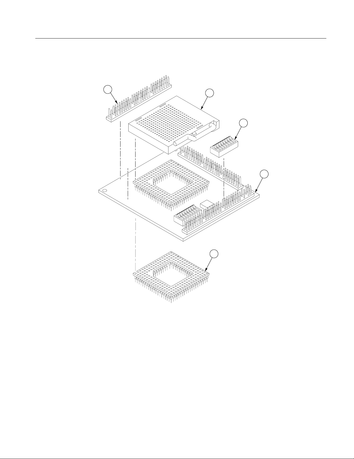
Replaceable Mechanical Parts
1
2
3
4
5
Figure 6–1: Exploded view of probe adapter
TMS 161 80960Cx Microprocessor Support Instruction Manual
6–5
Page 80

Replaceable Mechanical Parts
6–6
TMS 161 80960Cx Microprocessor Support Instruction Manual
Page 81

Index
Page 82

Page 83

Index
A
A0, A1 addressing signals, 2–12
about this manual set, ix
acquiring data, 2–7
Address group
channel assignments, 3–6
display column, 2–9
Alternate Bus Master cycles, 3–13
alternate connections
extra channel probes, 3–14
to other signals, 3–14
B
basic operations, where to find information, ix
Burst or Burst Pipelineing MOde, 2–12
bus cycles, displayed cycle types, 2–8
bus timing, 3–12
byte ordering, 1–2
C
certifications, 3–4
channel assignments
Address group, 3–6
clocks, 3–10
Control group, 3–8
Data group, 3–7
DataSize group, 3–8
Intr group, 3–9
Misc group, 3–9
channel groups, 2–1
clock channel assignments, 3–10
clock rate, 1–2
clocking, Custom, 2–1
how data is acquired, 3–11
clocking options, how data is acquired, 3–13
compliances, 3–4
connections
no probe adapter, 1–8
channel probes, 1–9
clock probes, 1–10
other microprocessor signals, 3–14
probe adapter to SUT, ZIF , 1–5
Control Flow display format, 2–10
Control group
channel assignments, 3–8
display column, 2–9
Custom clocking, 2–1
DMA cycles, 2–1
how data is acquired, 3–11
cycle types, 2–8
D
data
acquiring, 2–7
disassembly formats
Control Flow, 2–10
Hardware, 2–8
Software, 2–9
Subroutine, 2–11
how it is acquired, 3–11
data display , changing, 2–11
Data group
channel assignments, 3–7
display column, 2–9
DataSize group, channel assignments, 3–8
demonstration file, 2–13
dimensions, probe adapter, 3–5
disassembled data
cycle type definitions, 2–8
viewing, 2–7
viewing an example, 2–13
disassembler
definition, ix
logic analyzer configuration, 1–2
setup, 2–1
Disassembly Format Definition overlay, 2–11
Disassembly property page, 2–11
display formats
Control Flow, 2–10
Hardware, 2–8
Software, 2–9
special characters, 2–7
Subroutine, 2–11
DMA cycles, 2–1
TMS 161 80960Cx Microprocessor Support Instruction Manual
Index–1
Page 84

Index
E
electrical specifications, 3–2
environmental specifications, 3–4
H
Hardware display format, 2–8
cycle type definitions, 2–8
hardware reset, 1–3
I
installing hardware. See connections
Intr group, channel assignments, 3–9
L
leads (podlets), ZIF. See connections
Little-Endian byte ordering, 1–2
loading, electrical, 1–3
logic analyzer
configuration for disassembler, 1–2
software compatibility, 1–2
M
manual
conventions, ix
how to use the set, ix
Mark Cycle function, 2–13
Mark Opcode function, 2–13
marking cycles, definition of, 2–13
Memory region assignments, 2–11
microprocessor, specific clocking and how data is
acquired, 3–11
Misc group, channel assignments, 3–9
Mnemonic display column, 2–9
P
dimensions, 3–5
configuring, 1–3, 3–1
electrical loading, 1–3
hardware description, 3–1
jumper positions, 3–1
not using one, 1–8
placing the microprocessor in, ZIF, 1–7
R
reference memory, 2–13
reset, hardware, 1–3
restrictions, 1–2
without a probe adapter, 1–8
S
service information, 4–1
setups, disassembler, 2–1
signals
active low sign, x
alternate connections, 3–14
extra channel probes, 3–14
Software display format, 2–9
special characters displayed, 2–7
specifications, 3–1
certifications, 3–4
channel assignments, 3–5
compliances, 3–4
electrical, 3–2
environmental, 3–4
mechanical (dimensions), 3–5
Subroutine display format, 2–11
support setup, 2–1
SUT, definition, ix
synthesized signals, 3–13
T
terminology, ix
Timestamp display column, 2–9
probe adapter
alternate connections, 3–14
circuit description, 4–1
clearance, 1–5
adding sockets, 1–7
Index–2
V
viewing disassembled data, 2–7
TMS 161 80960Cx Microprocessor Support Instruction Manual
Page 85

Page 86

 Loading...