

Page 1

Instruction Manual
TMS 109
P54 & P55 Microprocessor Support
070-9811-00
There are no current European directives that
apply to this product. This product provides
cable and test lead connections to a test object of
electronic measuring and test equipment.
Warning
The servicing instructions are for use by
qualified personnel only. To avoid personal
injury, do not perform any servicing unless you
are qualified to do so. Refer to all safety
summaries prior to performing service.
Page 2

Copyright T ektronix, Inc. All rights reserved. Licensed software products are owned by Tektronix or its suppliers and are
protected by United States copyright laws and international treaty provisions.
Use, duplication, or disclosure by the Government is subject to restrictions as set forth in subparagraph (c)(1)(ii) of the
Rights in T echnical Data and Computer Software clause at DFARS 252.227-7013, or subparagraphs (c)(1) and (2) of the
Commercial Computer Software – Restricted Rights clause at F AR 52.227-19, as applicable.
T ektronix products are covered by U.S. and foreign patents, issued and pending. Information in this publication supercedes
that in all previously published material. Specifications and price change privileges reserved.
Printed in the U.S.A.
T ektronix, Inc., P.O. Box 1000, Wilsonville, OR 97070–1000
TEKTRONIX and TEK are registered trademarks of T ektronix, Inc.
Page 3

SOFTWARE WARRANTY
T ektronix warrants that the media on which this software product is furnished and the encoding of the programs on
the media will be free from defects in materials and workmanship for a period of three (3) months from the date of
shipment. If a medium or encoding proves defective during the warranty period, T ektronix will provide a
replacement in exchange for the defective medium. Except as to the media on which this software product is
furnished, this software product is provided “as is” without warranty of any kind, either express or implied.
T ektronix does not warrant that the functions contained in this software product will meet Customer’s
requirements or that the operation of the programs will be uninterrupted or error-free.
In order to obtain service under this warranty, Customer must notify Tektronix of the defect before the expiration
of the warranty period. If T ektronix is unable to provide a replacement that is free from defects in materials and
workmanship within a reasonable time thereafter, Customer may terminate the license for this software product
and return this software product and any associated materials for credit or refund.
THIS WARRANTY IS GIVEN BY TEKTRONIX IN LIEU OF ANY OTHER WARRANTIES, EXPRESS
OR IMPLIED. TEKTRONIX AND ITS VENDORS DISCLAIM ANY IMPLIED WARRANTIES OF
MERCHANTABILITY OR FITNESS FOR A PARTICULAR PURPOSE. TEKTRONIX’
RESPONSIBILITY TO REPLACE DEFECTIVE MEDIA OR REFUND CUSTOMER’S PAYMENT IS
THE SOLE AND EXCLUSIVE REMEDY PROVIDED TO THE CUSTOMER FOR BREACH OF THIS
WARRANTY. TEKTRONIX AND ITS VENDORS WILL NOT BE LIABLE FOR ANY INDIRECT,
SPECIAL, INCIDENTAL, OR CONSEQUENTIAL DAMAGES IRRESPECTIVE OF WHETHER
TEKTRONIX OR THE VENDOR HAS ADVANCE NOTICE OF THE POSSIBILITY OF SUCH
DAMAGES.
Page 4

HARDWARE WARRANTY
T ektronix warrants that the products that it manufactures and sells will be free from defects in materials and
workmanship for a period of one (1) year from the date of shipment. If a product proves defective during this
warranty period, T ektronix, at its option, either will repair the defective product without charge for parts and labor,
or will provide a replacement in exchange for the defective product.
In order to obtain service under this warranty, Customer must notify Tektronix of the defect before the expiration
of the warranty period and make suitable arrangements for the performance of service. Customer shall be
responsible for packaging and shipping the defective product to the service center designated by T ektronix, with
shipping charges prepaid. Tektronix shall pay for the return of the product to Customer if the shipment is to a
location within the country in which the T ektronix service center is located. Customer shall be responsible for
paying all shipping charges, duties, taxes, and any other charges for products returned to any other locations.
This warranty shall not apply to any defect, failure or damage caused by improper use or improper or inadequate
maintenance and care. T ektronix shall not be obligated to furnish service under this warranty a) to repair damage
resulting from attempts by personnel other than T ektronix representatives to install, repair or service the product;
b) to repair damage resulting from improper use or connection to incompatible equipment; c) to repair any
damage or malfunction caused by the use of non-T ektronix supplies; or d) to service a product that has been
modified or integrated with other products when the effect of such modification or integration increases the time
or difficulty of servicing the product.
THIS WARRANTY IS GIVEN BY TEKTRONIX IN LIEU OF ANY OTHER WARRANTIES, EXPRESS
OR IMPLIED. TEKTRONIX AND ITS VENDORS DISCLAIM ANY IMPLIED WARRANTIES OF
MERCHANTABILITY OR FITNESS FOR A PARTICULAR PURPOSE. TEKTRONIX’
RESPONSIBILITY TO REPAIR OR REPLACE DEFECTIVE PRODUCTS IS THE SOLE AND
EXCLUSIVE REMEDY PROVIDED TO THE CUST OMER FOR BREACH OF THIS WARRANTY.
TEKTRONIX AND ITS VENDORS WILL NOT BE LIABLE FOR ANY INDIRECT , SPECIAL,
INCIDENTAL, OR CONSEQUENTIAL DAMAGES IRRESPECTIVE OF WHETHER TEKTRONIX OR
THE VENDOR HAS ADVANCE NOTICE OF THE POSSIBILITY OF SUCH DAMAGES.
Page 5

Table of Contents
Getting Started
General Safety Summary vii. . . . . . . . . . . . . . . . . . . . . . . . . . . . . . . . . . . .
Service Safety Summary ix. . . . . . . . . . . . . . . . . . . . . . . . . . . . . . . . . . . . .
Preface: Microprocessor Support Documentation xi. . . . . . . . . . . . . . . .
Manual Conventions xi. . . . . . . . . . . . . . . . . . . . . . . . . . . . . . . . . . . . . . . . . . . . . .
Logic Analyzer Documentation xii. . . . . . . . . . . . . . . . . . . . . . . . . . . . . . . . . . . . . .
Contacting T ektronix xii. . . . . . . . . . . . . . . . . . . . . . . . . . . . . . . . . . . . . . . . . . . . . .
Support Description 1–1. . . . . . . . . . . . . . . . . . . . . . . . . . . . . . . . . . . . . . . . . . . . . . .
Logic Analyzer Software Compatibility 1–2. . . . . . . . . . . . . . . . . . . . . . . . . . . . . . .
Logic Analyzer Configuration 1–2. . . . . . . . . . . . . . . . . . . . . . . . . . . . . . . . . . . . . . .
Requirements and Restrictions 1–2. . . . . . . . . . . . . . . . . . . . . . . . . . . . . . . . . . . . . . .
Configuring the Probe Adapter 1–3. . . . . . . . . . . . . . . . . . . . . . . . . . . . . . . . . . . . . .
CLK Jumper 1–4. . . . . . . . . . . . . . . . . . . . . . . . . . . . . . . . . . . . . . . . . . . . . . . . .
Disassembly/Timing Jumper 1–4. . . . . . . . . . . . . . . . . . . . . . . . . . . . . . . . . . . . .
Tracking Jumper 1–6. . . . . . . . . . . . . . . . . . . . . . . . . . . . . . . . . . . . . . . . . . . . . .
Address Synthesis Jumper 1–6. . . . . . . . . . . . . . . . . . . . . . . . . . . . . . . . . . . . . .
D/P# Signal Jumper 1–6. . . . . . . . . . . . . . . . . . . . . . . . . . . . . . . . . . . . . . . . . . .
Connecting to a System Under T est 1–7. . . . . . . . . . . . . . . . . . . . . . . . . . . . . . . . . . .
Conventional Probe Adapter 1–7. . . . . . . . . . . . . . . . . . . . . . . . . . . . . . . . . . . . .
Low-Profile Probe Adapter with a High-Density Probe 1–10. . . . . . . . . . . . . . . .
Applying and Removing Power 1–14. . . . . . . . . . . . . . . . . . . . . . . . . . . . . . . . . . . . . .
Operating Basics
Setting Up the Support 2–1. . . . . . . . . . . . . . . . . . . . . . . . . . . . . . . . . . . . . .
Channel Group Definitions 2–1. . . . . . . . . . . . . . . . . . . . . . . . . . . . . . . . . . . . . . . . .
Clocking Options 2–1. . . . . . . . . . . . . . . . . . . . . . . . . . . . . . . . . . . . . . . . . . . . . . . . .
Symbols 2–2. . . . . . . . . . . . . . . . . . . . . . . . . . . . . . . . . . . . . . . . . . . . . . . . . . . . . . . .
Acquiring and Viewing Disassembled Data 2–5. . . . . . . . . . . . . . . . . . . . .
Acquiring Data 2–5. . . . . . . . . . . . . . . . . . . . . . . . . . . . . . . . . . . . . . . . . . . . . . . . . . .
Viewing Disassembled Data 2–5. . . . . . . . . . . . . . . . . . . . . . . . . . . . . . . . . . . . . . . .
Hardware Display Format 2–7. . . . . . . . . . . . . . . . . . . . . . . . . . . . . . . . . . . . . . .
Software Display Format 2–9. . . . . . . . . . . . . . . . . . . . . . . . . . . . . . . . . . . . . . .
Control Flow Display Format 2–9. . . . . . . . . . . . . . . . . . . . . . . . . . . . . . . . . . . .
Subroutine Display Format 2–10. . . . . . . . . . . . . . . . . . . . . . . . . . . . . . . . . . . . . .
Changing How Data is Displayed 2–10. . . . . . . . . . . . . . . . . . . . . . . . . . . . . . . . . . . .
Optional Display Selections 2–11. . . . . . . . . . . . . . . . . . . . . . . . . . . . . . . . . . . . .
Dual Microprocessors Execution Tracing 2–12. . . . . . . . . . . . . . . . . . . . . . . . . . .
Branch Trace Messages 2–14. . . . . . . . . . . . . . . . . . . . . . . . . . . . . . . . . . . . . . . .
Out-Of-Order Fetches 2–14. . . . . . . . . . . . . . . . . . . . . . . . . . . . . . . . . . . . . . . . . .
Speculative Prefetch Cycles 2–15. . . . . . . . . . . . . . . . . . . . . . . . . . . . . . . . . . . . .
Cache Invalidation Cycles 2–16. . . . . . . . . . . . . . . . . . . . . . . . . . . . . . . . . . . . . .
Burst Cycles 2–16. . . . . . . . . . . . . . . . . . . . . . . . . . . . . . . . . . . . . . . . . . . . . . . . .
System Management Mode (SMM) 2–16. . . . . . . . . . . . . . . . . . . . . . . . . . . . . . .
MMX Instruction Set 2–17. . . . . . . . . . . . . . . . . . . . . . . . . . . . . . . . . . . . . . . . . .
TMS 109 P54 & P55 Microprocessor Support Instruction Manual
i
Page 6

Table of Contents
Specifications
Maintenance
Marking Cycles 2–17. . . . . . . . . . . . . . . . . . . . . . . . . . . . . . . . . . . . . . . . . . . . . . .
Displaying Exception Vectors 2–18. . . . . . . . . . . . . . . . . . . . . . . . . . . . . . . . . . . .
Viewing an Example of Disassembled Data 2–20. . . . . . . . . . . . . . . . . . . . . . . . . . . .
Probe Adapter Description 3–1. . . . . . . . . . . . . . . . . . . . . . . . . . . . . . . . . . . . . . . . . .
Specifications 3–2. . . . . . . . . . . . . . . . . . . . . . . . . . . . . . . . . . . . . . . . . . . . . . . . . . . .
Mode Differences 3–16. . . . . . . . . . . . . . . . . . . . . . . . . . . . . . . . . . . . . . . . . . . . . . . . .
Component Mode 3–16. . . . . . . . . . . . . . . . . . . . . . . . . . . . . . . . . . . . . . . . . . . . .
Chip Set Mode 3–16. . . . . . . . . . . . . . . . . . . . . . . . . . . . . . . . . . . . . . . . . . . . . . .
How Data is Acquired 3–17. . . . . . . . . . . . . . . . . . . . . . . . . . . . . . . . . . . . . . . . . . . . .
Custom Clocking 3–17. . . . . . . . . . . . . . . . . . . . . . . . . . . . . . . . . . . . . . . . . . . . .
Clocking Options 3–19. . . . . . . . . . . . . . . . . . . . . . . . . . . . . . . . . . . . . . . . . . . . .
Alternate Microprocessor Connections 3–21. . . . . . . . . . . . . . . . . . . . . . . . . . . . . . . .
Signals Not On the Probe Adapter 3–23. . . . . . . . . . . . . . . . . . . . . . . . . . . . . . . .
Extra Channels 3–23. . . . . . . . . . . . . . . . . . . . . . . . . . . . . . . . . . . . . . . . . . . . . . .
Signals on the High-Density Probe 3–24. . . . . . . . . . . . . . . . . . . . . . . . . . . . . . . .
Probe Adapter Circuit Description 4–1. . . . . . . . . . . . . . . . . . . . . . . . . . . . . . . . . . . .
Replacing Signal Leads 4–3. . . . . . . . . . . . . . . . . . . . . . . . . . . . . . . . . . . . . . . . . . . .
Replacing Protective Sockets 4–3. . . . . . . . . . . . . . . . . . . . . . . . . . . . . . . . . . . . . . . .
Replacing the Fuse 4–3. . . . . . . . . . . . . . . . . . . . . . . . . . . . . . . . . . . . . . . . . . . . . . . .
Replaceable Electrical Parts
Parts Ordering Information 5–1. . . . . . . . . . . . . . . . . . . . . . . . . . . . . . . . . . . . . . . . .
Using the Replaceable Electrical Parts List 5–1. . . . . . . . . . . . . . . . . . . . . . . . . . . . .
Replaceable Mechanical Parts
Parts Ordering Information 6–1. . . . . . . . . . . . . . . . . . . . . . . . . . . . . . . . . . . . . . . . .
Using the Replaceable Mechanical Parts List 6–1. . . . . . . . . . . . . . . . . . . . . . . . . . .
Index
ii
TMS 109 P54 & P55 Microprocessor Support Instruction Manual
Page 7

List of Figures
Table of Contents
Figure 1–1: Jumper locations on the conventional probe adapter 1–5. . .
Figure 1–2: Jumper locations on the low-profile probe adapter 1–5. . . .
Figure 1–3: Placing a microprocessor into the conventional probe
adapter 1–8. . . . . . . . . . . . . . . . . . . . . . . . . . . . . . . . . . . . . . . . . . . . . . . .
Figure 1–4: Connecting probes to the conventional probe
adapter 1–9. . . . . . . . . . . . . . . . . . . . . . . . . . . . . . . . . . . . . . . . . . . . . . . .
Figure 1–5: Placing the conventional probe adapter onto the
SUT 1–10. . . . . . . . . . . . . . . . . . . . . . . . . . . . . . . . . . . . . . . . . . . . . . . . . . .
Figure 1–6: Placing a microprocessor into the low-profile probe
adapter 1–11. . . . . . . . . . . . . . . . . . . . . . . . . . . . . . . . . . . . . . . . . . . . . . . .
Figure 1–7: Placing the low-profile probe adapter onto the SUT 1–12. . . .
Figure 1–8: Connecting clock and channel probes to a high-density
probe 1–13. . . . . . . . . . . . . . . . . . . . . . . . . . . . . . . . . . . . . . . . . . . . . . . . . .
Figure 1–9: Connecting LO and HI cables to a high-density
probe 1–14. . . . . . . . . . . . . . . . . . . . . . . . . . . . . . . . . . . . . . . . . . . . . . . . . .
Figure 1–10: Power jack location on the conventional probe
adapter 1–15. . . . . . . . . . . . . . . . . . . . . . . . . . . . . . . . . . . . . . . . . . . . . . . .
Figure 1–11: Power jack location on the low-profile probe
adapter 1–16. . . . . . . . . . . . . . . . . . . . . . . . . . . . . . . . . . . . . . . . . . . . . . . .
Figure 2–1: Hardware display format 2–8. . . . . . . . . . . . . . . . . . . . . . . . . .
Figure 2–2: Data displayed from the Primary and Dual
microprocessors 2–13. . . . . . . . . . . . . . . . . . . . . . . . . . . . . . . . . . . . . . . . .
Figure 2–3: Disassembled data displayed from the Primary
microprocessor only 2–13. . . . . . . . . . . . . . . . . . . . . . . . . . . . . . . . . . . . .
Figure 2–4: Disassembled data displayed from the Dual
microprocessor only 2–14. . . . . . . . . . . . . . . . . . . . . . . . . . . . . . . . . . . . .
Figure 2–5: Display of target and source Branch Trace
Messages 2–14. . . . . . . . . . . . . . . . . . . . . . . . . . . . . . . . . . . . . . . . . . . . . . .
Figure 2–6: Speculative Prefetch cycles 2–16. . . . . . . . . . . . . . . . . . . . . . . .
Figure 3–1: Dimensions of the low-profile probe adapter 3–5. . . . . . . . . .
Figure 3–2: Dimensions of the conventional probe adapter 3–6. . . . . . . .
Figure 3–3: Nonpipelined single and Burst Transfer cycles 3–18. . . . . . . .
Figure 3–4: Pipelined cycles 3–19. . . . . . . . . . . . . . . . . . . . . . . . . . . . . . . . . .
Figure 3–5: Location of J1140 and J1150 on the conventional
probe adapter 3–22. . . . . . . . . . . . . . . . . . . . . . . . . . . . . . . . . . . . . . . . . .
Figure 3–6: Location of J1700 and J1701 on the low-profile
probe adapter 3–22. . . . . . . . . . . . . . . . . . . . . . . . . . . . . . . . . . . . . . . . . .
TMS 109 P54 & P55 Microprocessor Support Instruction Manual
iii
Page 8

Table of Contents
List of Tables
Figure 4–1: Location of the fuse on the conventional probe
adapter 4–3. . . . . . . . . . . . . . . . . . . . . . . . . . . . . . . . . . . . . . . . . . . . . . . .
Figure 4–2: Location of the fuse on the low-profile probe
adapter 4–4. . . . . . . . . . . . . . . . . . . . . . . . . . . . . . . . . . . . . . . . . . . . . . . .
Table 1–1: Jumper positions and function 1–3. . . . . . . . . . . . . . . . . . . . . .
Table 1–2: Disassembly/Timing jumper information 1–4. . . . . . . . . . . . .
Table 1–3: Probe adapter exceptions for the 136-channel
module 1–8. . . . . . . . . . . . . . . . . . . . . . . . . . . . . . . . . . . . . . . . . . . . . . . .
Table 1–4: High-density probe exceptions for the 136-channel
module 1–12. . . . . . . . . . . . . . . . . . . . . . . . . . . . . . . . . . . . . . . . . . . . . . . .
Table 2–1: Control group symbol table definitions 2–2. . . . . . . . . . . . . . .
Table 2–2: Meaning of special characters in the display 2–6. . . . . . . . . .
Table 2–3: Cycle type definitions 2–7. . . . . . . . . . . . . . . . . . . . . . . . . . . . .
Table 2–4: Trace Processor and Other Processor field selections 2–12. . .
Table 2–5: Exception vectors for Real Addressing mode 2–18. . . . . . . . . .
Table 2–6: Exception vectors for Protected Addressing mode 2–19. . . . . .
Table 3–1: Jumper positions and function 3–2. . . . . . . . . . . . . . . . . . . . . .
Table 3–2: Electrical specifications 3–2. . . . . . . . . . . . . . . . . . . . . . . . . . . .
Table 3–3: Environmental specifications 3–4. . . . . . . . . . . . . . . . . . . . . . .
Table 3–4: Certifications and compliances 3–4. . . . . . . . . . . . . . . . . . . . . .
Table 3–5: Address group channel assignments 3–8. . . . . . . . . . . . . . . . . .
Table 3–6: Data group channel assignments 3–9. . . . . . . . . . . . . . . . . . . . .
Table 3–7: Data_Lo group channel assignments 3–10. . . . . . . . . . . . . . . . .
Table 3–8: Control group channel assignments 3–11. . . . . . . . . . . . . . . . . .
Table 3–9: DataSize group channel assignments 3–12. . . . . . . . . . . . . . . . .
Table 3–10: 136-channel module: Cache group channel
assignment 3–12. . . . . . . . . . . . . . . . . . . . . . . . . . . . . . . . . . . . . . . . . . . . .
Table 3–11: 136-channel module: Misc group channel
assignments 3–12. . . . . . . . . . . . . . . . . . . . . . . . . . . . . . . . . . . . . . . . . . . .
Table 3–12: 192-channel module: Cache group channel
assignments 3–13. . . . . . . . . . . . . . . . . . . . . . . . . . . . . . . . . . . . . . . . . . . .
Table 3–13: 192-channel module: Debug group channel
assignments 3–13. . . . . . . . . . . . . . . . . . . . . . . . . . . . . . . . . . . . . . . . . . . .
Table 3–14: 192-channel module: APIC group channel
assignments 3–14. . . . . . . . . . . . . . . . . . . . . . . . . . . . . . . . . . . . . . . . . . . .
iv
TMS 109 P54 & P55 Microprocessor Support Instruction Manual
Page 9

Table of Contents
Table 3–15: 192-channel module: Priv_Bus group channel
assignments 3–14. . . . . . . . . . . . . . . . . . . . . . . . . . . . . . . . . . . . . . . . . . . .
Table 3–16: 192-channel module: Parity group channel
assignments 3–14. . . . . . . . . . . . . . . . . . . . . . . . . . . . . . . . . . . . . . . . . . . .
Table 3–17: 192-channel module: Misc group channel
assignments 3–15. . . . . . . . . . . . . . . . . . . . . . . . . . . . . . . . . . . . . . . . . . . .
Table 3–18: Clock channel assignments 3–16. . . . . . . . . . . . . . . . . . . . . . . .
Table 3–19: P54/P55 signals on J1140/J1700 3–21. . . . . . . . . . . . . . . . . . . .
Table 3–20: J1150/J1701 jumper pin assignments 3–23. . . . . . . . . . . . . . .
Table 3–21: Extra channels 3–24. . . . . . . . . . . . . . . . . . . . . . . . . . . . . . . . . .
Table 3–22: 136-channel module: Signals on the high-density
probe 3–24. . . . . . . . . . . . . . . . . . . . . . . . . . . . . . . . . . . . . . . . . . . . . . . . .
Table 4–1: Microprocessor signal delays when using the probe
adapter 4–2. . . . . . . . . . . . . . . . . . . . . . . . . . . . . . . . . . . . . . . . . . . . . . .
TMS 109 P54 & P55 Microprocessor Support Instruction Manual
v
Page 10

Table of Contents
vi
TMS 109 P54 & P55 Microprocessor Support Instruction Manual
Page 11

General Safety Summary
Review the following safety precautions to avoid injury and prevent damage to
this product or any products connected to it. To avoid potential hazards, use this
product only as specified.
While using this product, you may need to access other parts of the system. Read
the General Safety Summary in other system manuals for warnings and cautions
related to operating the system.
To Avoid Fire or
Personal Injury
Use Proper Power Cord. Use only the power cord specified for this product and
certified for the country of use.
Connect and Disconnect Properly . Do not connect or disconnect probes or test
leads while they are connected to a voltage source.
Observe All Terminal Ratings. To avoid fire or shock hazard, observe all ratings
and marking on the product. Consult the product manual for further ratings
information before making connections to the product.
Do not apply a potential to any terminal, including the common terminal, that
exceeds the maximum rating of that terminal.
Use Proper AC Adapter. Use only the AC adapter specified for this product.
Do Not Operate Without Covers. Do not operate this product with covers or panels
removed.
Use Proper Fuse. Use only the fuse type and rating specified for this product.
Avoid Exposed Circuitry. Do not touch exposed connections and components
when power is present.
Do Not Operate With Suspected Failures. If you suspect there is damage to this
product, have it inspected by qualified service personnel.
Do Not Operate in Wet/Damp Conditions.
Do Not Operate in an Explosive Atmosphere.
Keep Product Surfaces Clean and Dry .
Provide Proper Ventilation. Refer to the manual’s installation instructions for
details on installing the product so it has proper ventilation.
TMS 109 P54 & P55 Microprocessor Support Instruction Manual
vii
Page 12
General Safety Summary
Symbols and Terms
T erms in this Manual. These terms may appear in this manual:
WARNING. Warning statements identify conditions or practices that could result
in injury or loss of life.
CAUTION. Caution statements identify conditions or practices that could result in
damage to this product or other property.
T erms on the Product. These terms may appear on the product:
DANGER indicates an injury hazard immediately accessible as you read the
marking.
WARNING indicates an injury hazard not immediately accessible as you read the
marking.
CAUTION indicates a hazard to property including the product.
Symbols on the Product. The following symbols may appear on the product:
WARNING
High Voltage
Protective Ground
(Earth) T erminal
CAUTION
Refer to Manual
Double
Insulated
viii
TMS 109 P54 & P55 Microprocessor Support Instruction Manual
Page 13

Service Safety Summary
Only qualified personnel should perform service procedures. Read this Service
Safety Summary and the General Safety Summary before performing any service
procedures.
Do Not Service Alone. Do not perform internal service or adjustments of this
product unless another person capable of rendering first aid and resuscitation is
present.
Disconnect Power. To avoid electric shock, disconnect the main power by means
of the power cord or, if provided, the power switch.
Use Care When Servicing With Power On. Dangerous voltages or currents may
exist in this product. Disconnect power, remove battery (if applicable), and
disconnect test leads before removing protective panels, soldering, or replacing
components.
To avoid electric shock, do not touch exposed connections.
TMS 109 P54 & P55 Microprocessor Support Instruction Manual
ix
Page 14

Service Safety Summary
x
TMS 109 P54 & P55 Microprocessor Support Instruction Manual
Page 15

Preface: Microprocessor Support Documentation
This instruction manual contains specific information about the TMS 109
P54/P55 microprocessor support and is part of a set of information on how to
operate this product on compatible Tektronix logic analyzers.
If you are familiar with operating microprocessor supports on the logic analyzer
for which the TMS 109 P54/P55 support was purchased, you will probably only
need this instruction manual to set up and run the support.
If you are not familiar with operating microprocessor supports, you will need to
supplement this instruction manual with information on basic operations to set up
and run the support.
Information on basic operations of microprocessor supports is included with each
product. Each logic analyzer has basic information that describes how to perform
tasks common to supports on that platform. This information can be in the form
of online help, an installation manual, or a user manual.
This manual provides detailed information on the following topics:
H Connecting the logic analyzer to the system under test
Manual Conventions
H Setting up the logic analyzer to acquire data from the system under test
H Acquiring and viewing disassembled data
H Using the probe adapter
This manual uses the following conventions:
H The term disassembler refers to the software that disassembles bus cycles
into instruction mnemonics and cycle types.
H The phrase “information on basic operations” refers to online help, an
installation manual, or a basic operations of microprocessor supports user
manual.
H In the information on basic operations, the term XXX used in field selections
and file names must be replaced with P54C. This is the name of the
microprocessor in field selections and file names you must use to operate the
P54/P55 support.
H The term system under test (SUT) refers to the microprocessor-based system
from which data will be acquired.
TMS 109 P54 & P55 Microprocessor Support Instruction Manual
xi
Page 16

Preface: Microprocessor Support Documentation
H The term logic analyzer refers to the Tektronix logic analyzer for which this
product was purchased.
H The term module refers to a 136-channel or a 192-channel module.
H P54/P55 refers to all supported variations of the P54 and P55 micropro-
cessors unless otherwise noted.
H A pound sign (#) following a signal name indicates an active low signal.
Logic Analyzer Documentation
A description of other documentation available for each type of Tektronix logic
analyzer is located in the corresponding module user manual. The manual set
provides the information necessary to install, operate, maintain, and service the
logic analyzer and associated products.
Contacting Tektronix
Product
Support
Service
Support
For other
information
To write us Tektronix, Inc.
For application-oriented questions about a Tektronix measurement product, call toll free in North America:
1-800-TEK-WIDE (1-800-835-9433 ext. 2400)
6:00 a.m. – 5:00 p.m. Pacific time
Or, contact us by e-mail:
tm_app_supp@tek.com
For product support outside of North America, contact your
local Tektronix distributor or sales office.
Contact your local Tektronix distributor or sales office. Or, visit
our web site for a listing of worldwide service locations.
http://www.tek.com
In North America:
1-800-TEK-WIDE (1-800-835-9433)
An operator will direct your call.
P.O. Box 1000
Wilsonville, OR 97070-1000
xii
TMS 109 P54 & P55 Microprocessor Support Instruction Manual
Page 17

Getting Started
Page 18

Page 19

Getting Started
Support Description
This chapter provides information on the following topics and tasks:
H A description of the TMS 109 microprocessor support package
H Logic analyzer software compatibility
H Your system under test requirements
H Support restrictions
H How to configure the probe adapter
H How to connect to the system under test (SUT)
H How to apply power to and remove power from the probe adapter
The TMS 109 microprocessor support package disassembles data from systems
that are based on the Intel P54C, P54CM, P55C, and P55CM microprocessors.
The support runs on a compatible Tektronix logic analyzer equipped with a
136-channel module or a 192-channel module.
Refer to information on basic operations to determine how many modules and
probes your logic analyzer needs to meet the minimum channel requirements for
the TMS 109 microprocessor support.
The TMS 109 supports the P54C, P54CM, P55C, and P55CM microprocessors in
a 296-pin PGA package.
The low-profile probe adapter requires a 192-Channel High-Density Probe to
make connections from the logic analyzer to your SUT.
A complete list of standard and optional accessories is provided at the end of the
parts list in the Replaceable Mechanical Parts chapter.
To use this support efficiently, you need to have the items listed in the information on basic operations as well as the P54/P55 Microprocessor User’s Manual,
Intel, 1997.
Information on basic operations also contains a general description of supports.
TMS 109 P54 & P55 Microprocessor Support Instruction Manual
1–1
Page 20

Getting Started
Logic Analyzer Software Compatibility
The label on the microprocessor support floppy disk states which version of logic
analyzer software the support is compatible with.
Logic Analyzer Configuration
To use the TMS 109 support, the Tektronix logic analyzer must be equipped with
either a 136-channel module or a 192-channel module at a minimum. The
module must be equipped with enough probes to acquire clock and channel data
from signals in your P54/P55-based system.
Refer to information on basic operations to determine how many modules and
probes the logic analyzer needs to meet the channel requirements.
Requirements and Restrictions
You should review the general requirements and restrictions of microprocessor
supports in the information on basic operations as they pertain to your SUT.
You should also review electrical, environmental, and mechanical specifications
in the Specifications chapter in this manual as they pertain to your system under
test, as well as the following descriptions of other P54/P55 support requirements
and restrictions.
System Clock Rate. The TMS 109 support can acquire data from the P54/P55
microprocessor at speeds of up to 66.66 MHz
SUT Power. Whenever the SUT is powered off, be sure to remove power from
the probe adapter. Refer to Applying and Removing Power at the end of this
chapter for information on how to remove power from the probe adapter.
Disabling the Instruction Cache. To disassemble acquired data, you must disable
the internal instruction cache. Disabling the cache makes all instruction
prefetches visible on the bus so they can be acquired and disassembled.
Cache Invalidation Cycles. Cache Invalidation addresses are not acquired.
1
.
1–2
Bus Hold Cycles. Bus Hold cycles are not acquired while the RESET signal is
active.
1
Specification at time of printing. Contact your Tektronix sales representative for
current information on the fastest devices supported.
TMS 109 P54 & P55 Microprocessor Support Instruction Manual
Page 21
Getting Started
AHOLD Signal. If the AHOLD signal is active (high) during a Writeback cycle (a
four cycle Burst Write), the acquired address is undefined.
Burst Cycles. The P54/P55 microprocessor expects the memory system to
increment addresses during a Burst cycle. When viewing disassembled data, the
disassembler synthesizes the addresses. When viewing state data, the addresses
appear to be identical.
Probe Mode Cycles. Probe Mode cycles are not identified.
Directory T able and Descriptor Table Reads and Writes. These reads and writes are
not disassembled.
Bus Anomalies. Some combinations of instructions and operating modes of the
microprocessor can cause additional cycles to be fetched. This behavior is
unpredicatable, not documented, and can cause the disassembler to misinterpret if
fetched cycles were or were not executed. This is most likely to occur during
Floating Point operations.
Configuring the Probe Adapter
There are five jumpers on each probe adapter. Table 1–1 lists the jumper
positions and functions.
T able 1–1: Jumper positions and function
Conventional
probe adapter
J1 155 J1501 1–2
J1 160 J1500 1–2
J1 165 J1401 1–2
Low-profile
probe adapter
Position Function
Match the P54/P55 microprocessor system speed at 40–80 MHz
2–3
2–3
2–3
Match the P54/P55 microprocessor system speed at 25–50 MHz
Configure probe adapter for Custom clocking (disassembly)
Configure probe adapter for timing analysis
Enable tracking of burst and pipelined cycles while BOFF# and HLDA are asserted
Disable tracking of burst and pipelined cycles while BOFF# and HLDA are asserted. This
setting can be used if an external master’s signal timing is different from that of the P54C.
TMS 109 P54 & P55 Microprocessor Support Instruction Manual
1–3
Page 22
Getting Started
T able 1–1: Jumper positions and function (cont.)
Conventional
probe adapter
J1 170 J1400 1–2
J1340 J1404 1–2
Low-profile
probe adapter
2–3
OPEN
CLK Jumper
Disassembly/Timing
Jumper
FunctionPosition
Enable Address Synthesis (A(2:0) are derived from BE(7:0)#)
Disable Address Synthesis (A(2:0)=0)
Acquire the D/P# signal from pin AE35 of the socket being probed
Acquire the D/P# signal from an external source. If this jumper is left open, you must
route the D/P# signal to pin 1 of this jumper from an external source. This allows you to
probe your system from the Dual socket as long as the D/P# signal is accessible on the
system board.
The CLK jumper (J1155 on the conventional probe adapter or J1501 on the
low-profile probe adapter) should be placed in the ≥45 position to acquire data
from a system running at or faster than 45 MHz. The jumper should be placed in
the <45 position to acquire data from a system running slower than 45 MHz.
Figure 1–1 shows the location of J1155 on the conventional probe adapter;
Figure 1–2 shows the location of J1501 on the low-profile probe adapter.
The Disassembly/Timing jumper (J1160 on the conventional probe adapter or
J1500 on the low-profile probe adapter) should be placed in the D position to
acquire disassembled data and in the T position to acquire timing data.
Table 1–2 shows how to position this jumper depending on the type of clocking
you are using and the type of display you want to view.
T able 1–2: Disassembly/T iming jumper information
J1160/J1500 position Clocking Data window
D (Disassembly)
T (Timing) Internal Waveform window, or Timing
Custom Listing window, Disassembly,
State, or Graph displays
display
External Waveform window , Listing
window, or Timing display
Figure 1–1 shows the location of J1160 on the conventional probe adapter;
Figure 1–2 shows the location of J1500 on the low-profile probe adapter.
1–4
TMS 109 P54 & P55 Microprocessor Support Instruction Manual
Page 23
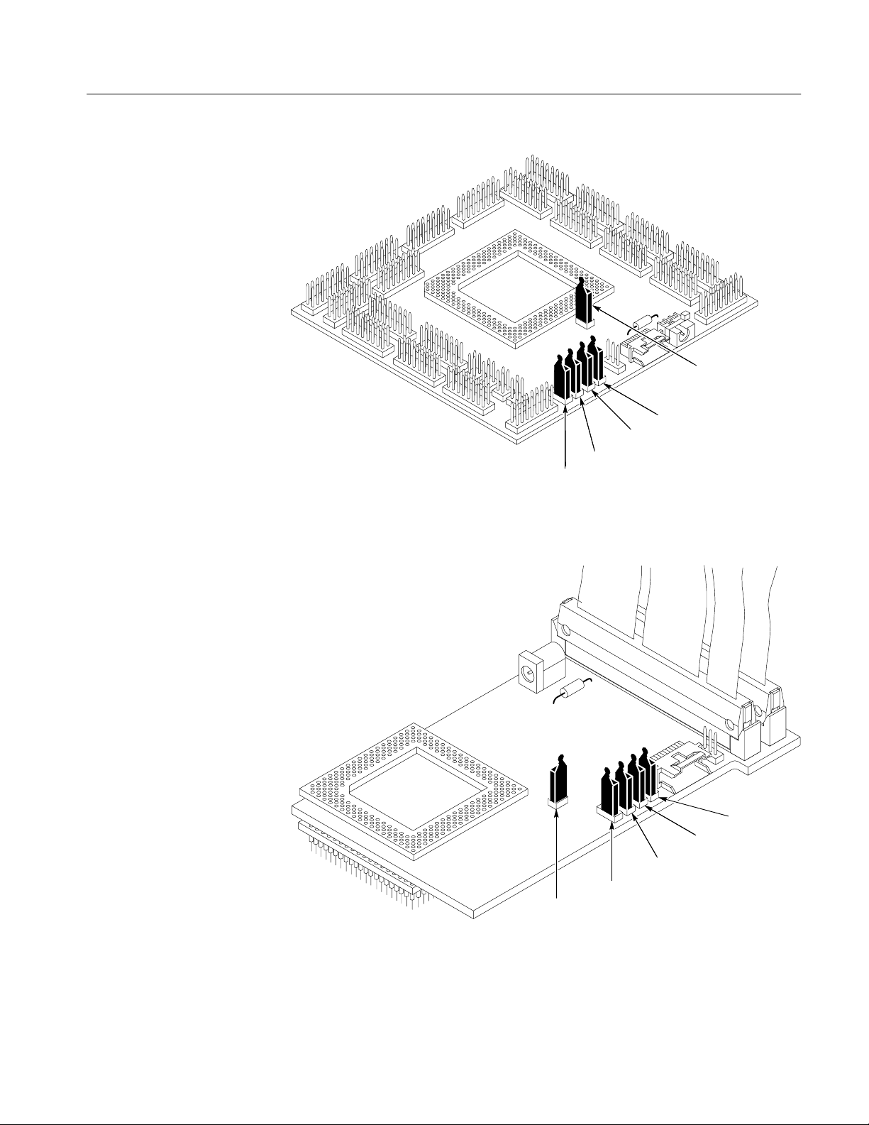
J1170
Getting Started
J1340
J1155
J1160
J1165
Figure 1–1: Jumper locations on the conventional probe adapter
J1401
J1400
J1404
J1501
J1500
Figure 1–2: Jumper locations on the low-profile probe adapter
TMS 109 P54 & P55 Microprocessor Support Instruction Manual
1–5
Page 24

Getting Started
Tracking Jumper
Address Synthesis
Jumper
The Tracking jumper (J1165 on the conventional probe adapter or J1401 on the
low-profile probe adapter) should not need to be moved from the default position
(pins 1 and 2 connected).
The only time this jumper should be moved is when the tracking circuitry
malfunctions. An indication of such a malfunction is when you see activity on
the bus during a BOFF or HLDA cycle that is uncharacteristic of the P54/P55
microprocessor. When the jumper is in the 2, 3 position, the circuitry on the
probe adapter does not track BOFF and HLDA cycles. A data sample will show
that such a cycle occurred but it will not contain meaningful information.
This jumper only affects the probe adapter when the Disassembly/Timing jumper
(J1160 on the conventional probe adapter or J1500 on the low-profile probe
adapter) is in the D position.
Figure 1–1 shows the location of J1165 on the conventional probe adapter;
Figure 1–2 shows the location of J1401 on the low-profile probe adapter.
When the Address Synthesis jumper (J1170 on the conventional probe adapter or
J1400 on the low-profile probe adapter) is in position 1, 2, A(2:0) are derived
from the BE(7:0)# signals and stored in the acquisition memory with the rest of
the address.
D/P# Signal Jumper
When the jumper is in position 2, 3, it disables address synthesis, A(2:0)=0.
Figure 1–1 shows the location of J1170 on the conventional probe adapter;
Figure 1–2 shows the location of J1400 on the low-profile probe adapter.
When the D/P# signal jumper (J1340 on the conventional probe adapter or J1404
on the low-profile probe adapter) is in the 1, 2 position, the D/P# signal is
acquired from pin AE35 of the socket being probed.
When the jumper is open (not connected), it acquires the D/P# signal from an
external source, and you will have to route the D/P# signal to pin 1 of this jumper
externally. This allows you to probe your system from the dual socket as long as
the D/P# signal is accessible on the SUT.
Figure 1–1 shows the location of J1340 on the conventional probe adapter;
Figure 1–2 shows the location of J1404 on the low-profile probe adapter.
1–6
TMS 109 P54 & P55 Microprocessor Support Instruction Manual
Page 25

Connecting to a System Under Test
Before you connect to the SUT, you must connect the probes to the module.
Your SUT must also have a minimum amount of clear space surrounding the
microprocessor to accommodate the probe adapter. Refer to the Specifications
chapter in this manual for the required clearances.
The channel and clock probes shown in this chapter are for a 136-channel
module. The probes will look different if you are using a 192-channel module.
The general requirements and restrictions of microprocessor supports in the
information on basic operations shows the vertical dimensions of a channel or
clock probe connected to square pins on a circuit board.
Getting Started
Conventional Probe
Adapter
To connect the logic analyzer to a SUT using a conventional PGA probe adapter,
follow these steps:
1. Turn off power to your SUT. It is not necessary to turn off power to the logic
analyzer.
CAUTION. Static discharge can damage the microprocessor, the probe adapter,
the probes, or the module. To prevent static damage, handle all of the above only
in a static-free environment.
Always wear a grounding wrist strap or similar device while handling the
microprocessor and probe adapter.
2. To discharge your stored static electricity, touch the ground connector located
on the back of the logic analyzer. Then, touch any of the ground pins of the
probe adapter to discharge stored static electricity from the probe adapter.
3. Place the probe adapter onto the antistatic shipping foam to support the probe
as shown in Figure 1–3. This prevents the circuit board from flexing and the
socket pins from bending.
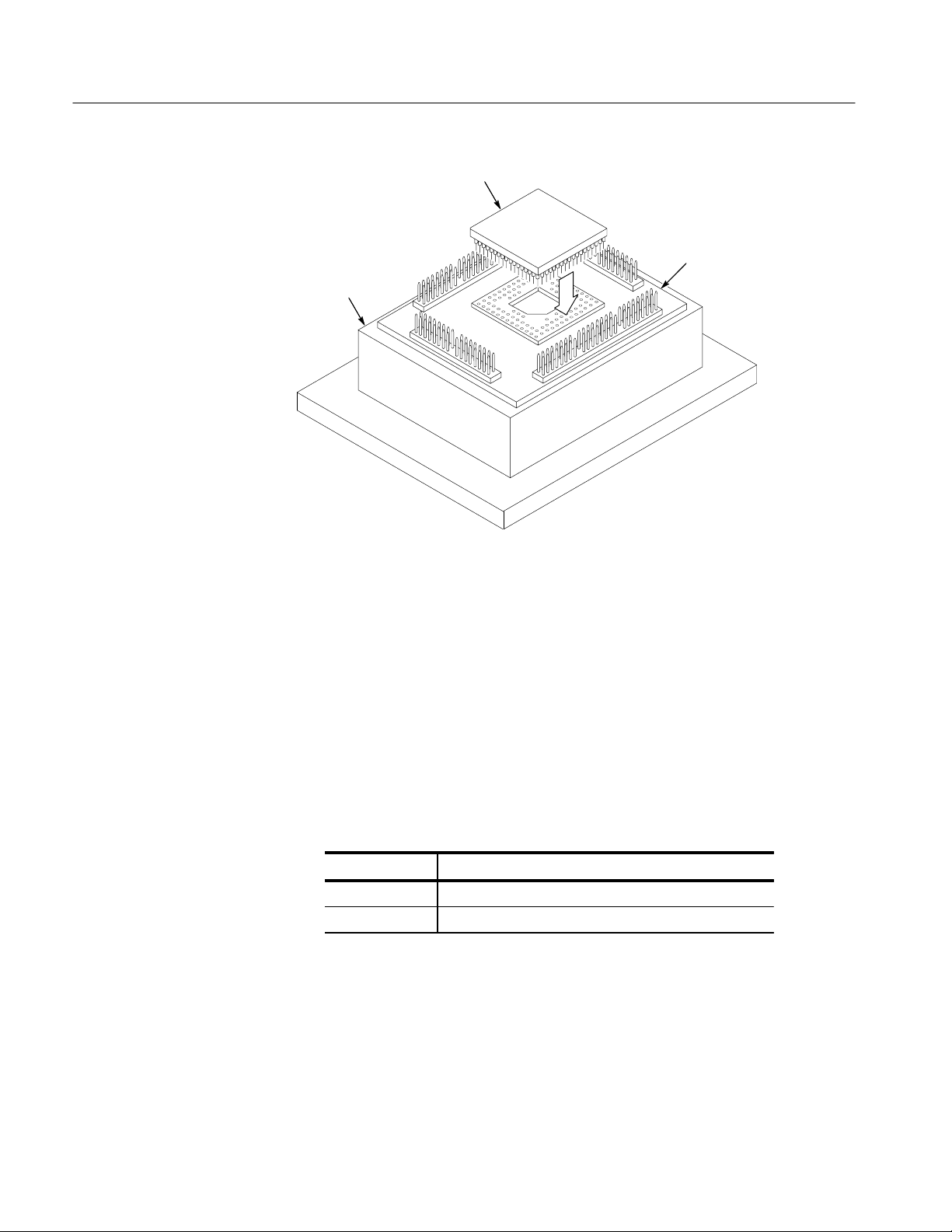
4. Remove the microprocessor from your SUT.
5. Line up the pin 2B indicator on the probe adapter board with the pin 2B
indicator on the microprocessor.
CAUTION. Failure to correctly place the microprocessor into the probe adapter
might permanently damage the microprocessor once power is applied.
6. Place the microprocessor into the probe adapter as shown in Figure 1–3.
TMS 109 P54 & P55 Microprocessor Support Instruction Manual
1–7
Page 26
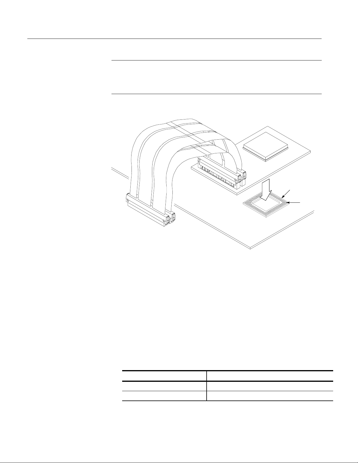
Getting Started
Microprocessor
Probe adapter
Foam
Figure 1–3: Placing a microprocessor into the conventional probe adapter
7. Connect the channel and clock probes to the probe adapter as shown in
Figure 1–4. For the 192-channel module, match the channel groups and
numbers on the probe labels to the corresponding HI_ and LO_pins on the
probe adapter. Match the ground pins on the probes to the corresponding pins
on the probe adapter.
For the 136-channel module, match the channel groups and numbers on the
probe labels to the corresponding LO_ pins on the probe apapter. There are
some exceptions; they are shown in Table 1–3.
T able 1–3: Probe adapter exceptions for the 136-channel module
Section Connect to probe adapter pins
E3, E2, E1, E0 HI_A3, HI_A2, HI_A1, HI_A0
C1, C0 HI_C3, HI_C2
1–8
TMS 109 P54 & P55 Microprocessor Support Instruction Manual
Page 27
Getting Started
8-channel probe
and podlet holder
Hold the channel probes by the podlet
holder when connecting them to the
probe adapter. Do not hold them by
the cables or necks of the podlets.
Foam
Clock probe
Figure 1–4: Connecting probes to the conventional probe adapter
Probe adapter
8. Line up the pin 2B indicator on the probe adapter board with the pin 2B
indicator on your SUT.
9. Place the probe adapter onto the SUT as shown in Figure 1–5.
NOTE. You might need to stack one or more replacement sockets between the SUT
and the probe adapter to provide sufficient vertical clearance from adjacent
components. However, keep in mind that this might increase loading, which can
reduce the electrical performance of your probe adapter.
TMS 109 P54 & P55 Microprocessor Support Instruction Manual
1–9
Page 28
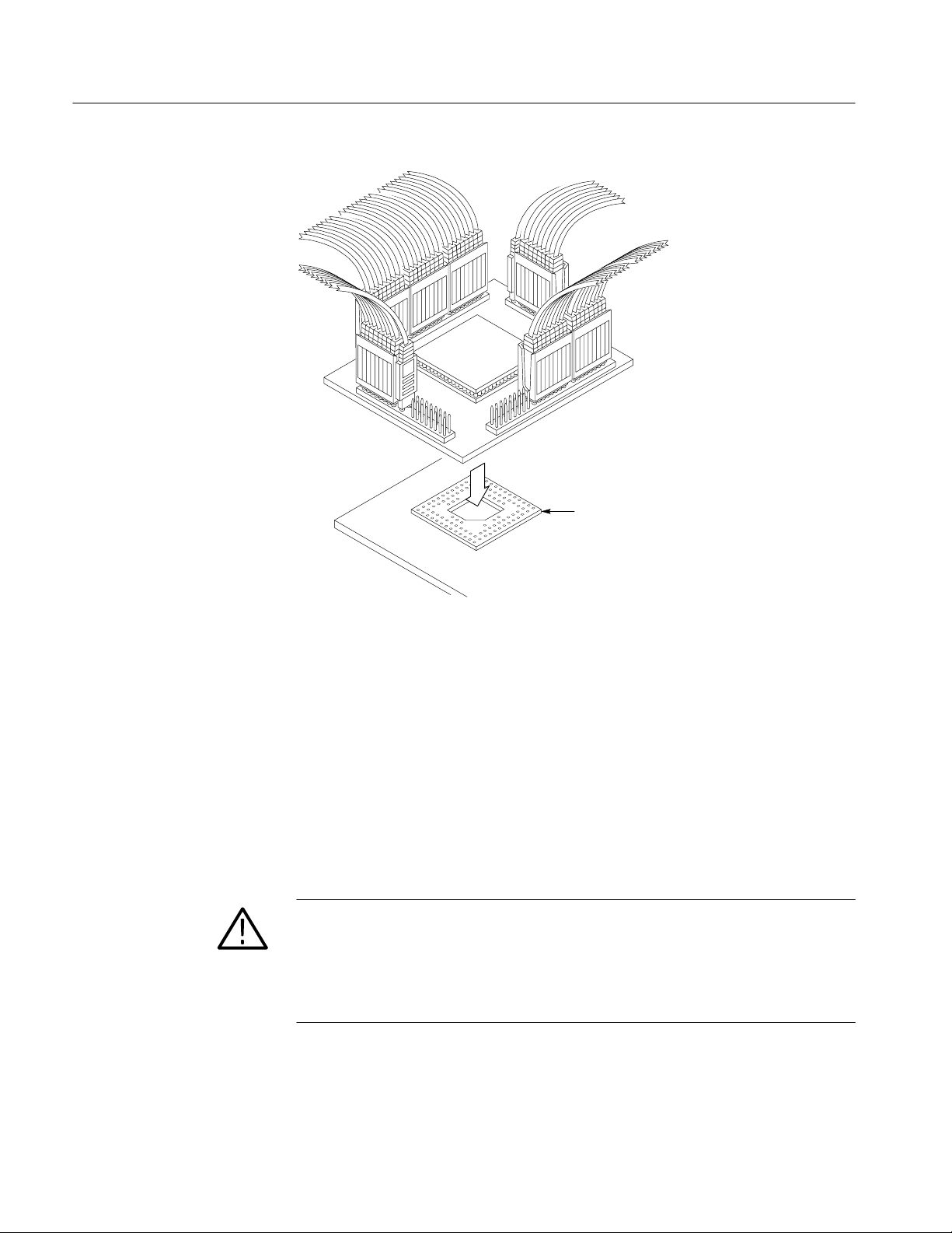
Getting Started
SUT socket
Low-Profile Probe Adapter
with a High-Density Probe
Figure 1–5: Placing the conventional probe adapter onto the SUT
If a probe adapter has one or two high-density cables (probe adapter does not
have pins to which the channel and clock probes connect), the probe adapter
requires a high-density probe to make connections between the logic analyzer
and a SUT.
To connect the logic analyzer to a SUT using the low-profile PGA probe adapter
and a high-density probe, follow these steps:
1. Turn off power to your SUT. It is not necessary to turn off power to the logic
analyzer.
CAUTION. Static discharge can damage the microprocessor, the low-profile probe
adapter, the probes, or the module. To prevent static damage, handle all of the
above only in a static-free environment.
Always wear a grounding wrist strap or similar device while handling the
microprocessor and low-profile probe adapter.
1–10
TMS 109 P54 & P55 Microprocessor Support Instruction Manual
Page 29
Getting Started
2. To discharge your stored static electricity, touch the ground connector located
on the back of the logic analyzer. Then, touch the black foam on the
underside of the probe adapter to discharge stored static electricity from the
probe adapter.
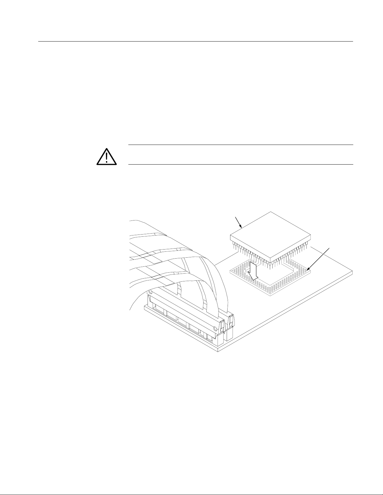
3. Remove the microprocessor from the SUT.
4. Line up the pin 2B indicator on the probe adapter board with the pin 2B
indicator on the microprocessor.
CAUTION. Failure to correctly place the microprocessor into the probe adapter
might permanently damage the microprocessor once power is applied.
5. Place the microprocessor into the probe adapter as shown in Figure 1–6.
Microprocessor
Pin 2B
Figure 1–6: Placing a microprocessor into the low-profile probe adapter
6. Remove the black foam from the underside of the probe adapter.
7. Line up the pin 2B indicator on the probe adapter board with the pin 2B
indicator on the SUT.
8. Place the probe adapter onto the SUT as shown in Figure 1–7.
TMS 109 P54 & P55 Microprocessor Support Instruction Manual
1–11
Page 30
Getting Started
NOTE. You might need to stack one or more replacement sockets between the SUT
and the probe adapter to provide sufficient vertical clearance from adjacent
components. However, keep in mind this might increase loading, which can
reduce the electrical performance of the probe adapter.
SUT socket
Pin 2B
Figure 1–7: Placing the low-profile probe adapter onto the SUT
9. Connect the clock and channel probes to the high-density probe as shown in
Figure 1–8. For the 192-channel module, match the channel groups and
numbers on the probe labels to the corresponding HI_ and LO_pins on the
high-density probe. Match the ground pins on the probes to the corresponding pins on the probe adapter.
For the 136-channel module, match the channel groups and numbers on the
probe labels to the corresponding LO_ pins on the high-density probe. There
are some exceptions; they are shown in Table 1–4.
T able 1–4: High-density probe exceptions for the 136-channel module
Section Connect to high-density probe pins
E3, E2, E1, E0 HI_A3, HI_A2, HI_A1, HI_A0
C1, C0 HI_C3, HI_C2
1–12
TMS 109 P54 & P55 Microprocessor Support Instruction Manual
Page 31

Getting Started
Match the ground pins on the probes to the corresponding pins on the probe
adapter.
Clock probe
Hold the 8-channel probes by the
podlet holder when connecting them to
the high-density probe. Do not hold
them by the cables or necks of the
podlets.
8-channel probe
and podlet holder
Channels connect to
the logic analyzer
High-density probe
Figure 1–8: Connecting clock and channel probes to a high-density probe
10. Align pin 1 on the LO cable connector, the end on the narrowest cable strip
of the cable, with pin 1 on the LO connector on the high-density probe.
Connect the cable to the connector as shown in Figure 1–9.
NOTE. The LO cable is 12 inches long; the HI cable is 13 inches long.
11. Align pin 1 on the HI cable connector, the end on the narrowest cable strip of
the cable, with pin 1 on the HI connector on the high-density probe. Connect
the cable to the connector as shown in Figure 1–9.
TMS 109 P54 & P55 Microprocessor Support Instruction Manual
1–13
Page 32

Getting Started
HI cable
Pin 1 end
LO cable
High-density probe
Figure 1–9: Connecting LO and HI cables to a high-density probe
Applying and Removing Power
A power supply for the P54/P55 probe adapter is included with the support. The
power supply provides +5 volts power to the probe adapter. The center connector
of the power jack connects to Vcc.
NOTE. Whenever the SUT is powered off, be sure to remove power from the probe
adapter.
1–14
TMS 109 P54 & P55 Microprocessor Support Instruction Manual
Page 33

Getting Started
To apply power to the P54/P55 probe adapter and SUT, follow these steps:
CAUTION. Failure to use the +5 V power supply provided by Tektronix might
permanently damage the probe adapter and P54/P55 microprocessor. Do not
mistake another power supply that looks similar for the +5 V power supply.
1. Connect the +5 V power supply to the jack on the probe adapter. Figure 1–10
shows the location of the jack on the conventional probe adapter. Figure 1–11
shows the location of the jack on the low-profile probe adapter.
CAUTION. Failure to apply power to the probe adapter before applying power to
your SUT might permanently damage the P54/P55 microprocessor and SUT.
2. Plug the power supply for the probe adapter into an electrical outlet.
3. Power on the SUT.
Figure 1–10: Power jack location on the conventional probe adapter
TMS 109 P54 & P55 Microprocessor Support Instruction Manual
Power jack
1–15
Page 34

Getting Started
Power jack
Figure 1–11: Power jack location on the low-profile probe adapter
To remove power from the SUT and P54/P55 probe adapter, follow these steps:
CAUTION. Failure to power down your SUT before removing the power from the
probe adapter might permanently damage the P54/P55 microprocessor and SUT.
1. Power off the SUT.
2. Unplug the power supply for the probe adapter from the electrical outlet.
1–16
TMS 109 P54 & P55 Microprocessor Support Instruction Manual
Page 35

Operating Basics
Page 36

Page 37

Setting Up the Support
This section provides information on how to set up the support. Information
covers the following topics:
H Channel group definitions
H Clocking options
H Symbol table files
Remember that the information in this section is specific to the operations and
functions of the TMS 109 P54/P55 support on any Tektronix logic analyzer for
which it can be purchased. Information on basic operations describes general
tasks and functions.
Before you acquire and disassemble data, you need to load the support and
specify setups for clocking and triggering as described in the information on
basic operations. The support provides default values for each of these setups,
but you can change them as needed.
Channel Group Definitions
Clocking Options
The software automatically defines channel groups for the support. For the
136-channel module, the channel groups for the P54/P55 support are Address,
Data, Data_Lo, Control, DataSize, Cache, and Misc. For the 192-channel
module, the channel groups for the P54/P55 support are Address, Data, Data_Lo,
Control, DataSize, Cache, Debug, APIC, Priv_Bus, Parity, and Misc. If you want
to know which signal is in which group, refer to the channel assignment tables
beginning on page 3–7.
The TMS 109 support offers a microprocessor-specific clocking mode for the
P54/P55 microprocessors. This clocking mode is the default selection whenever
you load the P54C support.
A description of how cycles are sampled by the module using the TMS 109
support and probe adapter is found in the Specifications chapter.
Disassembly will not be correct with the Internal or External clocking modes.
Information on basic operations describes how to use these clock selections for
general purpose analysis.
TMS 109 P54 & P55 Microprocessor Support Instruction Manual
2–1
Page 38

Setting Up the Support
Symbols
The clocking option for the TMS 109 support is Alternate Bus Master Cycles.
An alternate bus master cycle is defined as the cycle in which the P54/P55
microprocessor gives up the bus to an alternate device (a DMA device or another
microprocessor). These types of cycles are acquired when you select Included.
Backoff cycles will always be acquired regardless of the Alternate Bus Master
Cycles selection.
The TMS 109 support supplies one symbol table file. The P54C_Ctrl file
replaces specific Control channel group values with symbolic values when
Symbolic is the radix for the channel group.
Table 2–1 shows the name, bit pattern, and meaning for the symbols in the file
P54C_Ctrl, the Control channel group symbol table.
T able 2–1: Control group symbol table definitions
Control group value
D/P# BUSCHK# LAST_D M/IO#
Symbol
INIT SMIACT# AHOLD D/C#
IRESET_L LOCK# HLDA W/R#
PRDY SCYC BOFF#
Meaning
Reset
Primary processor opcode read
Dual processor opcode read
Opcode read
Primary processor locked read cycle
Dual processor locked read cycle
Locked read cycle
Primary processor locked write cycle
Dual processor locked write cycle
Locked write cycle
Primary processor nonopcode read
Dual processor nonopcode read
Read from memory, nonopcode
Primary processor write to memory
Dual processor write to memory
Write to memory
2–2
TMS 109 P54 & P55 Microprocessor Support Instruction Manual
Page 39

T able 2–1: Control group symbol table definitions (cont.)
Control group value
D/P# BUSCHK# LAST_D M/IO#
Symbol Meaning
INIT SMIACT# AHOLD D/C#
IRESET_L LOCK# HLDA W/R#
P_I/O_RD 0X0 XXXX XXX0 1010
D_I/O_RD 1X0 XXXX XXX0 1010
I/O_RD* XX0 XXXX XXX0 1010
P_I/O_WR 0X0 XXXX XXX0 1011
D_I/O_WR 1X0 XXXX XXX0 1011
I/O_WR* XX0 XXXX XXX0 1011
P_MEM_R/W* 0X0 XXXX XXX0 111X
D_MEM_R/W* 1X0 XXXX XXX0 111X
MEM_R/W* XX0 XXXX XXX0 111X
P_I/O_R/W* 0X0 XXXX XXX0 101X
D_I/O_R/W* 1X0 XXXX XXX0 101X
I/O_R/W* XX0 XXXX XXX0 101X
P_READ* 0X0 XXXX XXX0 1X10
D_READ* 1X0 XXXX XXX0 1X10
READ* XX0 XXXX XXX0 1X10
P_WRITE* 0X0 XXXX XXX0 1X11
D_WRITE* 1X0 XXXX XXX0 1X11
WRITE* XX0 XXXX XXX0 1X11
P_INT_ACK 0X0 XXXX XXX0 1000
D_INT_ACK 1X0 XXXX XXX0 1000
INT_ACK* XX0 XXXX XXX0 1000
P_SPECIAL 0X0 XXXX XXX0 1001
D_SPECIAL 1X0 XXXX XXX0 1001
SPECIAL* XX0 XXXX XXX0 1001
P_RESERVE 0X0 XXXX XXX0 1101
D_RESERVE 1X0 XXXX XXX0 1101
RESERVE* XX0 XXXX XXX0 1101
ALT_B_MTR XX0 XXXX XXX1 XXXX
BOFF XX0 XXXX XXXX 0XXX
PRDY SCYC BOFF#
Primary processor I/O read cycle
Dual processor I/O read cycle
I/O read cycle
Primary processor I/O write cycle
Dual processor I/O write cycle
I/O write cycle
Any primary processor read or write
Any dual processor read or write
Any memory read or write cycle
Any primary processor I/O cycle
Any dual processor I/O cycle
Any I/O read or write cycle
Any primary processor read cycle
Any dual processor read cycle
Any read cycle
Any primary processor write cycle
Any dual processor write cycle
Any write cycle
Primary processor int. acknowledge
Dual processor int. acknowledge
Interrupt acknowledge cycle
Primary processor special cycle
Dual processor special cycle
Special cycle
Primary processor reserved
Dual processor reserved
Reserved
Alternate bus master cycle
Backoff cycle
Setting Up the Support
TMS 109 P54 & P55 Microprocessor Support Instruction Manual
2–3
Page 40

Setting Up the Support
T able 2–1: Control group symbol table definitions (cont.)
Control group value
D/P# BUSCHK# LAST_D M/IO#
Symbol Meaning
INIT SMIACT# AHOLD D/C#
IRESET_L LOCK# HLDA W/R#
P_BUSCHCK 0X0 X0XX XXX0 1XXX
D_BUSCHCK 1X0 X0XX XXX0 1XXX
BUSCHCK* XX0 X0XX XXX0 1XXX
P_LOCKED 0X0 X1X0 XXXX XXXX
D_LOCKED 1X0 X1X0 XXXX XXXX
LOCKED* XX0 X1X0 XXXX XXXX
P_SPLTCYC* 0X0 X1X0 1XXX XXXX
D_SPLTCYC* 1X0 X1X0 1XXX XXXX
SPLTCYC* XX0 X1X0 1XXX XXXX
P_SMM* 0X0 XX0X XXXX XXXX
D_SMM* 1X0 XX0X XXXX XXXX
SMM* XX0 XX0X XXXX XXXX
PRIMARY* 0XX XXXX XXXX XXXX
DUAL* 1XX XXXX XXXX XXXX
*
Symbols used only for triggering; they are not displayed.
PRDY SCYC BOFF#
Primary processor buscheck
Dual processor buscheck
Buscheck
Any primary processor locked cycle
Any dual processor locked cycle
Any locked cycle
Primary processor split cycle
Dual processor split cycle
Split cycle
The primary processor is in smm
The dual processor is in smm
Either processor is in smm
Any primary processor cycle
Any dual processor cycle
Information on basic operations describes how to use symbolic values for
triggering and for displaying other channel groups symbolically, such as the
Address channel group.
2–4
TMS 109 P54 & P55 Microprocessor Support Instruction Manual
Page 41

Acquiring and Viewing Disassembled Data
This section describes how to acquire data and view it disassembled. Information
covers the following topics and tasks:
H Acquiring data
H Viewing disassembled data in various display formats
H Cycle type labels
H Changing the way data is displayed
H Changing disassembled cycles with the mark cycles function
Acquiring Data
Once you load the P54C support, choose a clocking mode, and specify the
trigger, you are ready to acquire and disassemble
If you have any problems acquiring data, refer to information on basic operations
in your online help or Appendix A: Error Messages and Disassembly Problems in
the basic operations user manual.
data.
Viewing Disassembled Data
You can view disassembled data in four display formats: Hardware, Software,
Control Flow, and Subroutine. The information on basic operations describes
how to select the disassembly display formats.
NOTE. Selections in the Disassembly property page (the Disassembly Format
Definition overlay) must be set correctly for your acquired data to be disassembled correctly. Refer to Changing How Data is Displayed on page 2–10.
The default display format shows the Address, Data, Data_Lo, and Control
channel groups for each sample of acquired data. The Data and Data_Lo groups
are shown in one column.
The disassembler displays special characters and strings in the instruction
mnemonics to indicate significant events. Table 2–2 shows these special
characters and strings, and gives a definition of what they represent.
TMS 109 P54 & P55 Microprocessor Support Instruction Manual
2–5
Page 42

Acquiring and Viewing Disassembled Data
T able 2–2: Meaning of special characters in the display
Character or string displayed Meaning
or m
The instruction was manually marked as a program fetch
****
#
(16) or (32)
SMM
(MMX)
-ā-ā
-
* ILLEGAL INSTRUCTION *
Indicates there is insufficient data available for complete
disassembly of the instruction; the number of asterisks
indicates the width of the data that is unavailable. Each two
asterisks represent one byte.
Indicates an immediate value
Indicates that the fetch is from a 16- or 32-bit code segment
size and disassembled accordingly. If the mnemonic fills the
entire column width, the (16) or (32) will not be displayed.
Indicates a System management mode cycle.
Indicates an MMX instruction; appears at the end of the
mnemonic
Hyphens (–) in the Data column indicate invalid bytes as
determined by the BE7#-BE0# signals. When one of the two
data groups does not contain valid bytes for a nonfetch
cycle, the line for the group with the invalid bytes is not
displayed. When neither data group contains valid bytes,
both lines are displayed; this is an unexpected condition.
A hyphen in front of a cycle type label indicates a bus cycle
from the microprocessor not being traced.
Decoded as an illegal instruction
2–6
Logic analyzer software does not allow more than 32 channels in each channel
group. Therefore, two channel groups are used to acquire 64-bit wide P54/P55
microprocessor data: Data (D63-D32) and Data_Lo (D31-D0).
To handle the display of disassembled data from both data groups, the
disassembler may display more than one line for each data sample. For samples
with two display lines, data displayed under the Data column of the first line is
from the Data_Lo group (D31-0); data displayed under the Data column of the
second line is from the Data group (D63-32). Figure 2–1 on page 2–8 shows
examples of multiple display lines used to display Data_Lo and Data group
information.
The disassembler synthesizes the A2-A0 signals.
Aborting Lengthy Disassembly . When acquiring data from two microprocessors,
the disassembler might take a long time to display disassembled data. This could
be caused by the combination of selections in the Trace Processor and Other
Processor fields in the Disassembly property page (Disassembly Format
Definition overlay).
TMS 109 P54 & P55 Microprocessor Support Instruction Manual
Page 43

Acquiring and Viewing Disassembled Data
An example where this might occur is when the Trace Processor field is set to
DUAL, and the Other Processor field is set to Suppress. If the acquisition data
only contains data from the Primary microprocessor, then the disassembler might
take a long time to display disassembled cycle types or instruction mnemonics.
You can interrupt the disassembler by hitting the Break Key. If the disassembler
does not find any displayable data, it will revert back to the Hardware display
format with default settings.
Hardware Display Format
In Hardware display format, the disassembler displays certain cycle type labels in
parentheses. Table 2–3 shows these cycle type labels and gives a definition of the
cycle they represent. Reads to interrupt and exception vectors will be labeled
with the vector name.
The disassembler always displays at least one line of information. Because
fetches should have valid data for the Data and Data_Lo groups, most fetches
should use at least two display lines. For example, a fetch cycle can show both an
instruction, and a READ EXTENSION or FLUSH (or both).
T able 2–3: Cycle type definitions
Label Description
( RESET )
( MEM READ )
( LOCKED MEM READ )
( MEM WRITE )
( LOCKED MEM WRITE )
( IO READ )
( IO WRITE )
A reset cycle
A nonlocked memory read cycle that is not an opcode fetch
A locked memory read cycle that is not an opcode fetch
Any nonlocked memory write
Any locked memory write
Read from an I/O port
Write to an I/O port
( INT ACK )
( SHUTDOWN )
( CACHE FLUSH )
( HALT )
( WRITE-BACK )
( FLUSH ACK )
( BRANCH TRACE: TARGET )
( BRANCH TRACE: SOURCE )
( STOP GRANT ACK )
( RESERVED )
( ALTERNATE BUS MASTER )
Interrupt acknowledge cycle
Shutdown/special bus cycle; BE7:BE0 = 11111110
Cache flush/special bus cycle; BE7:BE0 = 1 1111101
Halt/special bus cycle; BE7:BE0 = 11111011
Write back/special bus cycle; BE7:BE0 = 1 111011 1
Flush Ack/special bus cycle; BE7:BE0 = 1 1101111
Branch Trace Message/special bus cycle; BE7:BE0 = 1101 1111
Branch Trace Message/special bus cycle; BE7:BE0 = 1101 1111
Stop Grant cycle; cycle type is HAL T/SPECIAL;
BE7:BE0 = 1111101 1
Reserved
Bus is released to an Alternate Bus Master
TMS 109 P54 & P55 Microprocessor Support Instruction Manual
2–7
Page 44

Acquiring and Viewing Disassembled Data
T able 2–3: Cycle type definitions (Cont.)
Label Description
( BACK OFF )
Back Off bus cycle
( UNKNOWN )
( BURST LINE FILL )*
An invalid/unknown bus cycle
Fetch cycle computed to be a burst fill. The data is fetched but
will not be executed, it is part of a 32 byte fetch. It will possibly
be stored in cache.
( BACKOFF/BURST FLUSH )*
( EXTENSION )*
( FLUSH )*
( DUAL FETCH )
( PRIMARY FETCH )
Burst/Fetch cycle computed to be flushed due to a back off
Fetch cycle computed to be an opcode extension
Fetch cycle computed to be flushed
Nondisassembled fetch cycle from the Dual processor
Nondisassembled fetch cycle from the Primary processor
* Computed cycle types. * Computed cycle types.
Figure 2–1 shows an example of the Hardware display.
1 2 3
Sample Address Data Mnemonic Timestamp
-------------------------------------------------------------------------------000388AE FF33F633 XOR EDI,EDI (32)
15 000408A0 C033CB00 - ( DUAL FETCH ) 100 ns
000408A4 C933DB33 - ( DUAL FETCH )
4
5
16 000388B0 ABFFE1C3 RETS (32) 100 ns
000388B4 B6EFFFEF ( FLUSH )
17 000408A8 ED33D233 - ( DUAL FETCH ) 100 ns
000408AC FF33F633 - ( DUAL FETCH )
18 000388B8 FFB7D7FA ( FLUSH ) 100 ns
000388BC FFFFFDFF ( FLUSH )
19 000408B0 BDDF26C3 - ( DUAL FETCH ) 100 ns
000408B4 FF27FFBF - ( DUAL FETCH )
20 000207F4 00000005 ( MEM READ ) 100 ns
21 000408B8 5DBE5FED - ( DUAL FETCH ) 100 ns
000408BC 7FFEFBFB - ( DUAL FETCH )
22 000388C0 44875050 ( FLUSH ) 100 ns
000388C4 04870824 ( FLUSH )
23 000307F4 00000005 - ( MEM READ ) 100 ns
24 00038800 00009DE8 ( FLUSH ) 100 ns
00038805 000EBE00 MOV ESI,#0000000E (32)
25 000408C0 44875050 - ( DUAL FETCH ) 100 ns
000408C4 04870824 - ( DUAL FETCH )
6 7
2–8
Figure 2–1: Hardware display format
TMS 109 P54 & P55 Microprocessor Support Instruction Manual
Page 45

Acquiring and Viewing Disassembled Data
1
Sample Column. Lists the memory locations for the acquired data.
2
Address Group. Lists data from channels connected to the P54/P55 address
bus.
3
Data Column. Lists data from channels connected to D63-D32 and/or
D31-D0 of the P54/P55 microprocessor data bus. Refer to the general
description of viewing disassembled data for information on how the
disassembler determines when to display information for the Data group.
4
This part of the sample is displaying data from channels connected to
D31-D0 of the P54/P55 microprocessor data bus.
5
This part of the sample is displaying data from channels connected to
D63-D32 of the P54/P55 microprocessor data bus.
6
Mnemonic Column. Lists the disassembled instructions and cycle types.
7
Timestamp. Lists the timestamp values when a timestamp selection is made.
Information on basic operations describes how you can select a timestamp.
Software Display Format
Control Flow Display
Format
The Software display format shows only the first fetch of executed instructions.
Flushed cycles and extensions are not shown, even though they are part of the
executed instruction. Read extensions will be used to disassemble the instruction,
but will not be displayed as a separate cycle in the Software display format. Data
reads and writes are not displayed.
Out-of-order fetches are shown in the order the fetches are executed. An asterisk
indicates an out-of-order fetch. The sample number of the out-of-order fetch will
not be displayed if the previous executed instruction has a higher sample number.
The sample number of the out-of-order fetch will be displayed if the previous
executed instruction has a smaller sample number.
Since you cannot place the cursor on an instruction without a sample number,
you will not be able to scroll to some out-of-order fetch instructions. To scroll to
these instructions, you will have to switch to the Hardware display format.
The Control Flow display format shows only the first fetch of instructions that
change the flow of control.
Instructions that generate a change in the flow of control in the P54/P55
microprocessor are as follows:
CALL IRET RET
INT JMP RSM
TMS 109 P54 & P55 Microprocessor Support Instruction Manual
2–9
Page 46

Acquiring and Viewing Disassembled Data
Instructions that might generate a change in the flow of control in the P54/P55
microprocessor are as follows:
BOUND JL/JNGE JNP/JPO
DIV JLE/JNG JNS
IDIV JNB/JAE/JNC JO
INTO JNBE/JA JP/JPE
JB/JNAE/JC JNE/JNZ JS
JBE/JNA JNL/JGE LOOP
JCXZ/JECXZ JNLE/JG LOOPNZ/LOOPNE
JE/JZ JNO LOOPZ/LOOPE
If a conditional jump branches to an address that is reached sequentially (no
address break in the fetch sample), the disassembler cannot determine if the
branch was taken. If there are two conditional jump instructions close together
that branch to the same fetch line, then the disassembler may not be able to
determine which conditional jump was actually taken. You can use the mark
cycle function to correct the disassembly. Refer to Marking Cycles later in this
section.
Subroutine Display
Format
The Subroutine display format shows only the first fetch of subroutine call and
return instructions. It will display conditional subroutine calls if they are
considered to be taken.
Instructions that generate a subroutine call or a return in the P54/P55 microprocessor are as follows:
CALL INT IRET RET RSM
Instructions that might generate a subroutine call or a return in the P54/P55
microprocessor are as follows:
BOUND DIV IDIV INTO
Changing How Data is Displayed
There are common fields and features that allow you to further modify displayed
data to suit your needs. You can make common and optional display selections in
the Disassembly property page (the Disassembly Format Definition overlay).
You can make selections unique to the P54/P55 support to do the following tasks:
H Change how data is displayed across all display formats
2–10
H Change the interpretation of disassembled cycles
H Display exception vectors
TMS 109 P54 & P55 Microprocessor Support Instruction Manual
Page 47

Acquiring and Viewing Disassembled Data
NOTE. All information defined in these fields pertain to the microprocessor that is
being traced.
Optional Display
Selections
You can make optional selections for disassembled
common selections (described in the information on basic operations), you can
change the displayed data in the following ways:
H Specify the code segment size
H Choose an interrupt table
H Specify the starting address of the interrupt table
H Specify the size of the interrupt table
H Select to trace the Primary or Dual microprocessor
H Choose whether to display or suppress the hardware cycles from the
microprocessor not being traced
The P54/P55 support has six additional fields: Code Segment Size, Interrupt
Table, Interrupt Table Address, Interrupt Table Size, Trace Processor, and Other
Processor. These fields appear in the area indicated in the information on basic
operations.
Code Segment Size. You can select the default code size: 32-bit or 16-bit. The
default code size is 16 bit.
data. In addition to the
Interrupt Table. You can specify if the interrupt table is Real, Virtual, or Protected.
(Selecting Virtual is equivalent to selecting Protected.) The default is Real.
Interrupt Table Address. You can specify the starting address of the interrupt table
in hexadecimal. The default starting address is 0x00000000.
Interrupt Table Size. You can specify the size of the interrupt table in hexadecimal.
The default size is 0x400.
Trace Processor. You can select to disassemble data from the Primary or Dual
microprocessor.
Other Processor. The “other” microprocessor is the one not being traced (not
selected in the Trace Processor field). You can select to display or to suppress its
bus cycles.
TMS 109 P54 & P55 Microprocessor Support Instruction Manual
2–11
Page 48

Acquiring and Viewing Disassembled Data
Dual Microprocessors
Execution Tracing
When acquiring data from a SUT with two microprocessors, the disassembler
can trace the execution flow of one microprocessor and display the hardware
cycle types of the microprocessor not being traced. This means that the software
disassembles only the instructions executed from the microprocessor being
traced.
You can trace instructions from either the Primary microprocessor or the Dual
microprocessor. You can also choose to display or not display (suppress) data
from the microprocessor not selected in the Trace Processor field of the
Disassembly property page (Disassembly Format Definition overlay).
To set up the mode of tracing, you need to set the Trace Processor and Other
Processor fields in the Disassembly property page. Table 2–4 shows the
combinations of Trace Processor and Other Processor field selections and their
effects.
T able 2–4: Trace Processor and Other Processor field selections
Trace Processor Other Processor Effect
Primary Suppress Disassemble the Primary microprocessor only
Primary Display Cycles Disassemble the Primary microprocessor and
display the hardware cycles of the Dual
microprocessor
Dual Suppress Disassemble the Dual microprocessor only
Dual Display Cycles Disassemble the Dual microprocessor and
display the hardware cycles of the Primary
microprocessor
Figure 2–2 shows disassembled data from the Primary microprocessor and
hardware cycles from the other microprocessor. A hyphen to the left of the
mnemonic indicates data from the other microprocessor.
2–12
TMS 109 P54 & P55 Microprocessor Support Instruction Manual
Page 49

Acquiring and Viewing Disassembled Data
Sample Address Data Mnemonic Control
-------------------------------------------------------------------------------16 000388B0 ABFFE1C3 RETS (32) P_FETCH
000388B4 B6EFFFEF ( FLUSH ) P_FETCH
17 000408A8 ED33D233 - ( DUAL FETCH ) D_FETCH
000408AC FF33F633 - ( DUAL FETCH ) D_FETCH
18 000388B8 FFB7D7FA ( FLUSH ) P_FETCH
000388BC FFFFFDFF ( FLUSH ) P_FETCH
19 000408B0 BDDF26C3 - ( DUAL FETCH ) D_FETCH
000408B4 FF27FFBF - ( DUAL FETCH ) D_FETCH
20 000207F4 00000005 ( MEM READ ) P_MEM_RD
21 000408B8 5DBE5FED - ( DUAL FETCH ) D_FETCH
000408BC 7FFEFBFB - ( DUAL FETCH ) D_FETCH
22 000388C0 44875050 ( FLUSH ) P_FETCH
000388C4 04870824 ( FLUSH ) P_FETCH
23 000307F4 00000005 - ( MEM READ ) D_MEM_RD
24 00038800 00009DE8 ( FLUSH ) P_FETCH
00038805 000EBE00 MOV ESI,#0000000E (32) P_FETCH
25 000408C0 44875050 - ( DUAL FETCH ) D_FETCH
000408C4 04870824 - ( DUAL FETCH ) D_FETCH
26 0003880A 0AB90000 MOV ECX,#0000000A (32) P_FETCH
0003880F F3000000 REPZ (32) P_FETCH
Figure 2–2: Data displayed from the Primary and Dual microprocessors
Figure 2–3 shows disassembled data from the Primary microprocessor only. Data
from the Dual microprocessor is suppressed and not displayed.
Sample Address Data Mnemonic Control
-------------------------------------------------------------------------------16 000388B0 ABFFE1C3 RETS (32) P_FETCH
000388B4 B6EFFFEF ( FLUSH ) P_FETCH
18 000388B8 FFB7D7FA ( FLUSH ) P_FETCH
000388BC FFFFFDFF ( FLUSH ) P_FETCH
20 000207F4 00000005 ( MEM READ ) P_MEM_RD
22 000388C0 44875050 ( FLUSH ) P_FETCH
000388C4 04870824 ( FLUSH ) P_FETCH
24 00038800 00009DE8 ( FLUSH ) P_FETCH
00038805 000EBE00 MOV ESI,#0000000E (32) P_FETCH
26 0003880A 0AB90000 MOV ECX,#0000000A (32) P_FETCH
0003880F F3000000 REPZ (32) P_FETCH
28 00038810 003668AD LODSD (32) P_FETCH
00038811 003668AD PUSH #00000036 (32) P_FETCH
00038816 026A0000 PUSH #02 (32) P_FETCH
30 00038818 4668026A PUSH #02 (32) P_FETCH
0003881A 4668026A PUSH #00000046 (32) P_FETCH
0003881F 6A000000 PUSH #02 (32) P_FETCH
Figure 2–3: Disassembled data displayed from the Primary microprocessor only
TMS 109 P54 & P55 Microprocessor Support Instruction Manual
2–13
Page 50

Acquiring and Viewing Disassembled Data
Figure 2–4 shows disassembled data from the Dual microprocessor only. Data
from the Primary microprocessor is suppressed and not displayed.
Sample Address Data Mnemonic Control
-------------------------------------------------------------------------------17 000408A8 ED33D233 XOR EDX,EDX (32) D_FETCH
000408AA ED33D233 XOR EBP,EBP (32) D_FETCH
000408AC FF33F633 XOR ESI,ESI (32) D_FETCH
000408AE FF33F633 XOR EDI,EDI (32) D_FETCH
19 000408B0 BDDF26C3 RETS (32) D_FETCH
000408B4 FF27FFBF ( FLUSH ) D_FETCH
21 000408B8 5DBE5FED ( FLUSH ) D_FETCH
000408BC 7FFEFBFB ( FLUSH ) D_FETCH
23 000307F4 00000005 ( MEM READ ) D_MEM_RD
25 000408C0 44875050 ( FLUSH ) D_FETCH
000408C4 04870824 ( FLUSH ) D_FETCH
27 00040800 00009DE8 ( FLUSH ) D_FETCH
00040805 000EBE00 MOV ESI,#0000000E (32) D_FETCH
29 0004080A 0AB90000 MOV ECX,#0000000A (32) D_FETCH
0004080F F3000000 REPZ (32) D_FETCH
Branch Trace Messages
Out-Of-Order Fetches
Figure 2–4: Disassembled data displayed from the Dual microprocessor only
The disassembler interprets the information on the Address and Data Bus of
Branch Trace Messages (BTMs) by reconstructing the address of the source or
target of the branch instruction. Depending on which type of BTM is in use,
either fast or normal, one or two BTMs will appear on the bus. The disassembler
tracks BTMs as they appear on the bus. Figure 2–5 shows how the disassembler
displays these cycles.
Sample Address Data Mnemonic Control
-------------------------------------------------------------------------------4 000207F4 00000005 ( MEM WRITE) P_MEM_WR
6 00038810 003868AD ( FLUSH ) P_FETCH
00038814 026A0000 ( FLUSH ) P_FETCH
8 000388A2 20------ ( BRANCH TRACE: TARGET ) P_SPECIAL
10 00038800 08------ ( BRANCH TRACE: SOURCE ) P_SPECIAL
14 00038818 33C03300 ( FLUSH ) P_FETCH
00038810 68C933DB ( FLUSH ) P_FETCH
Figure 2–5: Display of target and source Branch Trace Messages
The P54/P55 microprocessor can prefetch cycles out of ascending order. For
example, a branch to address 1008 could cause the following sample of addresses
across the bus: 1008, 1000, 1018, and 1010. The data at address 1008 is
executed, but the data at address 1000 is not. The data at addresses 1018 and
1010 are executed, but the data at address 1010 is executed before the data at
1018.
2–14
TMS 109 P54 & P55 Microprocessor Support Instruction Manual
Page 51

Acquiring and Viewing Disassembled Data
An example of the fetched order versus the executed order is shown below.
Fetched Order Executed Order
1008 1008
1000 1010
1018 1018
1010
In the Hardware display format, the out-of-order fetches are displayed in the
order they are fetched. They will be properly disassembled and identified by an
asterisk (*) to the left of the instruction.
In the Hardware display format, you can determine the executed order of the
out-of-order fetches by looking at the address of the out-of-order cycles and the
subsequent cycles. Fetch cycles always have the sample numbers displayed.
In the Software display format, out-of-order fetches are displayed in the order
they were executed. If the previously executed instruction had a larger sample
number than the out-of-order fetch, the sample number will not be displayed. If
the previous sample number is smaller than the out-of-order fetch, the sample
number will be displayed. To mark an instruction without a sample number, you
will have to switch to the Hardware display format.
Speculative Prefetch
Cycles
In the Software display format, out-of-order fetches can cause up to sixteen lines
of information to need to be displayed but only eight lines will actually be
displayed. The disassembler displays <more> in the Mnemonic column to
indicate that more than eight lines are available. To view more than eight lines of
information, you must use the Hardware display format.
Speculative prefetch cycles can occur when the P54/P55 microprocessor fetches
instructions that have been previously executed. To minimize prefetch delays, the
P54/P55 microprocessor predicts the outcome of the branch instruction and starts
prefetching at that address. When the branch instruction is executed, the target
address is determined. If the P54/P55 microprocessor predicted the target address
correctly, then the needed code has already been fetched. If it did not correctly
predict the target address, then the speculative prefetch cycles that had been
fetched will be flushed and fetching will begin at the target address.
Figure 2–6 shows an example of speculative prefetch cycles. The previous time
(not shown) that the JNE instruction was executed, the branch was taken and the
new target address was 0x3893D. The microprocessor assumed that the address
would be 0x3893D and so started fetching at 0x38938 (which contains
0x3893D). Cycles at samples 746 and 748 are speculative prefetch cycles. When
the instruction was executed, the microprocessor determined that the branch was
not taken, flushed the speculative prefetch cycles, and started fetching at
0x38988 (sample 750), which contained the next instruction after the JNE.
TMS 109 P54 & P55 Microprocessor Support Instruction Manual
2–15
Page 52

Acquiring and Viewing Disassembled Data
Sample Address Data Mnemonic Control
--------------------------------------------------------------------------------
734 000207D8 00000008 ( MEM READ ) P_MEM_RD
736 000207E8 00000046 ( MEM READ ) P_MEM_RD
738 00038988 000000BA ( FLUSH ) P_FETCH
740 00038990 20C2619D ( FLUSH ) P_FETCH
742 00038998 CDBFDE6F ( FLUSH ) P_FETCH
744 000389A0 FFFFEDAE ( FLUSH ) P_FETCH
746 00038938 DB9BFF33 ( FLUSH ) P_FETCH
748 00038940 6D8A0000 ( FLUSH ) P_FETCH
750 00038988 000000BA MOV EDX,#00000000 (32) P_FETCH
Figure 2–6: Speculative Prefetch cycles
00038986 B575C90F JNE 0003893D (32) P_FETCH
0003898C 24558900 ( FLUSH ) P_FETCH
00038994 6FBF6D00 ( FLUSH ) P_FETCH
0003899C FFEFFFF7 ( FLUSH ) P_FETCH
000389A4 F6FFF7EF ( FLUSH ) P_FETCH
0003893C 0002A3E3 ( FLUSH ) P_FETCH
00038944 204D8A10 ( FLUSH ) P_FETCH
0003898D 24558900 MOV 24[EBP],EDX (32) P_FETCH
Cache Invalidation Cycles
Burst Cycles
System Management
Mode (SMM)
NOTE. The microprocessor also has a Branch Target Buffer and often performs
speculative prefetching of branch target addresses (no matter if they are taken or
are not taken). The disassembler usually interprets the correct flow of execution
but cannot do so deterministically.
Cache Invalidation cycles are needed to keep the microprocessor cache contents
consistent with external memory. On a nonburst cycle that is also a Cache
Invalidation cycle, the data and address will be valid as probed. On a burst cycle
that is also a Cache Invalidation cycle, the data will be valid, but the addresses
will not be valid as probed and the software will try to calculate the address from
the surrounding cycles. Fetch cycles are disassembled. A letter c to the left of the
mnemonic indicates a Cache Invalidation cycle, where the AHOLD signal was
active.
On all burst cycles, only the first cycle contains a valid address. The P54/P55
microprocessor doesn’t increment the address for a burst. The disassembler
calculates the remaining burst cycle addresses for display.
The P54/P55 microprocessor provides a special mode called System Management Mode where the P54/P55 microprocessor CPU executes code from a
separate, alternate memory space called SMRAM. The disassembler uses
information from the SMIACT# signal to determine when the P54/P55 microprocessor is operating in this mode.
2–16
TMS 109 P54 & P55 Microprocessor Support Instruction Manual
Page 53

Acquiring and Viewing Disassembled Data
MMX Instruction Set
Marking Cycles
The P55 microprocessor includes the MMX instruction set. Since these instructions are potential subroutine instructions, the disassembler checks to see if an
interrupt level 6 (illegal opcode) or 7 (device not available) occurred. If an
interrupt 6 or 7 occurs, the interrupt will flush the bus.
When the disassembler detects that an instruction is from the MMX set, it
displays an (MMX) to the right of the mnemonic.
MMX instructions are disassembled whether or not the microprocessor is set up
to execute them.
The disassembler has a Mark Opcode function that allows you to change the
interpretation of a cycle type. Using this function, you can select a cycle and
change it to one of the following cycle types:
H Opcode (the first word of an instruction)
H Extension (a subsequent word of an instruction)
H Flush (an opcode or extension that is fetched but not executed)
H Anything (any valid opcode, extension or flush)
H 16-bit or 32-bit default segment size
Mark selections are as follows:
Lo: Any Any Any OPCODE
Lo: Any Any OPCODE Any
Lo: Any OPCODE Any Any
Lo: OPCODE Any Any Any
Hi: Any Any Any OPCODE
Hi: Any Any OPCODE Any
Hi: Any OPCODE Any Any
Hi: OPCODE Any Any Any
EXTENSION CYCLE
FLUSH CYCLE
16Ćbit Default Segment Size
32Ćbit Default Segment Size
Undo marks on this cycle
For samples with two display lines, to change the cycle type to an Opcode or
Anything, you must use the selections starting with Lo: for the first display line,
and selections starting with Hi: for the second display line.
TMS 109 P54 & P55 Microprocessor Support Instruction Manual
2–17
Page 54

Acquiring and Viewing Disassembled Data
You can also use the Mark Opcode function to specify the default segment size
mode (16-bit or 32-bit) for the cycle. The segment size selection changes the
cycle the cursor is on and the remaining cycles to the end of memory or to the
next mark.
The default segment size of the cycle is independent of any prefix override bytes
in the particular fetch. For example, if you mark cycle 455 with a default size of
32 bits, but there are address/operand override prefixes in the instruction, the
default size will be 32 bits but the size of the instruction will be 16 bits.
Information on basic operations contains more details on marking cycles.
Displaying Exception
Vectors
The disassembler can display exception vectors. You can select to display the
interrupt vectors for Real, Virtual, or Protected modes in the Interrupt Table field.
(Selecting Virtual is equivalent to selecting Protected.)
You can relocate the table by entering the starting address in the Interrupt Table
Address field. The Interrupt Table Address field provides the disassembler with
the offset address; enter an eight-digit hexadecimal value corresponding to the
offset of the base address of the exception table. The Interrupt Table Size field
lets you specify a three-digit hexadecimal size for the table.
You can make these selections in the Disassembly property page (the Disassembly Format Definition overlay).
Table 2–5 lists the P54/P55 exception vectors for the Real Addressing mode.
T able 2–5: Exception vectors for Real Addressing mode
Exception
number
0 0000
1 0004
2 0008
3 000C
4 0010
5 0014
6 0018
7 001C
8 0020
9-1 1 0024-002C
12 0030
13 0034
14-15 0038-003C
16 0040
Location in IV* table
(in hexadecimal)
Displayed interrupt name
2–18
TMS 109 P54 & P55 Microprocessor Support Instruction Manual
Page 55

Acquiring and Viewing Disassembled Data
T able 2–5: Exception vectors for Real Addressing mode (cont.)
Exception
number
17-31 0044-007C
32-255 0080-03FC
* IV means interrupt vector.
Location in IV* table
(in hexadecimal)
Displayed interrupt name
RESERVED
USER DEFINED
Table 2–6 lists the P54/P55 exception vectors for the Protected Addressing mode.
T able 2–6: Exception vectors for Protected Addressing mode
Exception
number
0 0000
1 0008
2 0010
3 0018
4 0020
5 0028
6 0030
7 0038
8 0040
9 0048
10 0050
11 0058
12 0060
13 0068
14 0070
15 0078
16 0080
17 0088
18 0090
Location in IDT*
(in hexadecimal)
Displayed exception name
DIVIDE ERROR
DEBUG EXCEPTIONS
NMI INTERRUPT
BREAKPOINT INTERRUPT
INTO DETECTED OVERFLOW
BOUND RANGE EXCEEDED
INVALID OPCODE
DEVICE NOT AVAILABLE
DOUBLE FAULT
RESERVED
INVALID TSS
SEGMENT NOT PRESENT
STACK EXCEPTION
SEGMENT OVERRUN
PAGE FAULT
RESERVED
COPROCESSOR MODE
ALIGNMENT CHECK
MACHINE CHECK
19-31 0090-00F8
32-255 0100-07F8
* IDT means interrupt descriptor table.
TMS 109 P54 & P55 Microprocessor Support Instruction Manual
RESERVED
USER DEFINED
2–19
Page 56

Acquiring and Viewing Disassembled Data
Viewing an Example of Disassembled Data
A demonstration system file (or demonstration reference memory) is provided so
you can see an example of how your P54/P55 microprocessor bus cycles and
instruction mnemonics look when they are disassembled. Viewing the system file
is not a requirement for preparing the module for use and you can view it without
connecting the logic analyzer to your SUT.
Information on basic operations describes how to view the file.
2–20
TMS 109 P54 & P55 Microprocessor Support Instruction Manual
Page 57

Specifications
Page 58

Page 59

Specifications
This chapter contains the following information:
H Probe adapter description
H Specification tables
H Dimensions of the probe adapter
H Channel assignment tables
H Description of how the module acquires P54/P55 signals
H List of other accessible microprocessor signals and extra probe channels
Probe Adapter Description
The probe adapter is nonintrusive hardware that allows the logic analyzer to
acquire data from a microprocessor in its own operating environment with little
effect, if any, on that system. Information on basic operations contains a figure
showing the logic analyzer connected to a typical probe adapter. Refer to that
figure while reading the following description.
Configuration
The probe adapter consists of a circuit board and a socket for a P54/P55
microprocessor. The probe adapter connects to the microprocessor in the SUT.
Signals from the microprocessor-based system flow from the probe adapter to the
channel groups and through the probe signal leads to the module.
All circuitry on the probe adapter is powered from the supplied power adapter.
The probe adapter accommodates the Intel P54C, P54CM, P55C, and P55CM
microprocessors in a 273-pin PGA package.
The probe adapter contains jumpers that need to be in certain positions for proper
disassembly; Table 3–1 shows the jumper positions. For more information on
these jumpers, refer to the descriptions on page 1–4.
TMS 109 P54 & P55 Microprocessor Support Instruction Manual
3–1
Page 60

Specifications
T able 3–1: Jumper positions and function
Conventional
probe adapter
J1 155 J1501 1–2
J1 160 J1500 1–2
J1 165 J1401 1–2
J1 170 J1400 1–2
J1340 J1404 1–2
Low-profile
probe adapter
Specifications
Position Function
Match the P54/P55 microprocessor system speed at 40–80 MHz
2–3
2–3
2–3
2–3
OPEN
Match the P54/P55 microprocessor system speed at 25–50 MHz
Configure probe adapter for Custom clocking (disassembly)
Configure probe adapter for timing analysis
Enable tracking of burst and pipelined cycles while BOFF# and HLDA are asserted
Disable tracking of burst and pipelined cycles while BOFF# and HLDA are asserted. This
setting can be used if an external master’s signal timing is different from that of the P54C.
Enable Address Synthesis (A(2:0) are derived from BE(7:0)#)
Disable Address Synthesis (A(2:0)=0)
Acquire the D/P# signal from pin AE35 of the socket being probed
Acquire the D/P# signal from an external source. If this jumper is left open, you will have
to route the D/P# signal to pin 1 of this jumper from an external source. This allows you to
probe your system from the Dual socket as long as the D/P# signal is accessible on the
system board.
These specifications are for a probe adapter connected between a compatible
Tektronix logic analyzer and a SUT. Table 3–2 shows the electrical requirements
the SUT must produce for the support to acquire correct data.
In Table 3–2, for the 136-channel module, one podlet load is 20 k in parallel
with 2 pF. For the 192-channel module, one podlet load is 100 k in parallel
with 10 pF.
T able 3–2: Electrical specifications
Characteristics Requirements
SUT DC power requirements
Voltage 4.75-5.25 VDC
Current I max (calculated) 1.8 A
I typ (measured) 1.2 A
Probe adapter power supply requirements
Voltage 90-265 VAC
Current 1.1 A maximum at 100 VAC
Frequency 47-63 Hz
Power 25 W maximum
3–2
TMS 109 P54 & P55 Microprocessor Support Instruction Manual
Page 61

T able 3–2: Electrical specifications (cont.)
Characteristics Requirements
SUT clock
Clock rate Max. 66.66 MHz
Minimum setup and hold time required
BE7–0#, ADS#, W/R#, BRDY#, BRDYC#,
HLDA, PM0/BP0, PM1/BP1, BP2, BP3
6 ns (T su min) 0.5 ns (Th min)
Specifications
BOFF#, NA#, KEN#, AHOLD, PHIT#, INV ,
FERR#
All other signals 3.5 ns (Tsu min) 2 ns (Th min)
Measured typical SUT signal loading Conventional Low-profile
CLK 25 pF 26 pF 1 CY7B991 (standard)
A31–A3 8–15 pF 8–15 pF 1 74FCT162501AT
D63–D0 8–15 pF 10–17 pF 1 74FCT162501AT
BE7#–BE0# 16–18 pF 18–19 pF 1 74FCT162501AT in parallel with 22V10
PM0/BP0, PM1/BP1#, BP2, BP3 9–10 pF 10–17 pF 1 16V8
CACHE#, SCYC, M/IO#, D/C#, RESET,
D/P#, STPCLK#, EADS#, LOCK#,
SMIACT#, BUSCHK#, TDO
ADS#, W/R#, BRDY#, HLDA, ADSC# 8–12 pF 9–13 pF 1 22V10
BRDYC# 10 pF 10 pF 10K in parallel with 22V10
KEN# 15 pF 15 pF 10K in parallel with 74FCT646AT
PRDY, RESET, D/P# 16–19 pF 18–29 pF 1 74FCT162501AT
DP7-DP0 8–12 pF 13–15 pF 1 74FCT162501AT
BOFF#, NA#, AHOLD, PHIT#, INV , FERR# 1 1–13 pF 12–14 pF 1 74FCT646AT
All other signals 5–9 pF 5–9 pF 1 74FCT162501AT
Not connected signals 2 pF 2 pF none
2.5 ns (T su min) 2 ns (Th min)
Specification
AC load (by probe adapter) DC load
1 CY7B991 in parallel with 100 + 15 pF
(low-profile)
8–13 pF 10–16 pF 1 74FCT162501AT
TMS 109 P54 & P55 Microprocessor Support Instruction Manual
3–3
Page 62

Specifications
Table 3–3 shows the environmental specifications.
T able 3–3: Environmental specifications*
Characteristic Description
Temperature
Maximum operating
Minimum operating 0° C (+32° F)
Non-operating –55° C to +75° C (–67° to +167° F)
Humidity 10 to 95% relative humidity
Altitude
Operating 4.5 km (15,000 ft) maximum
Non-operating 15 km (50,000 ft) maximum
Electrostatic immunity The probe adapter is static sensitive
* Designed to meet Tektronix standard 062-2847-00 class 5.
[
Not to exceed P54/P55 microprocessor thermal considerations. Forced air cooling
might be required across the CPU.
+50° C (+122° F)[
Table 3–4 shows the certifications and compliances that apply to the probe
adapter.
T able 3–4: Certifications and compliances
EC Compliance There are no current European Directives that apply to this product.
3–4
Figure 3–2 shows the dimensions of the low-profile probe adapter. The figure
also shows the minimum vertical clearance of the high-density probe cable.
TMS 109 P54 & P55 Microprocessor Support Instruction Manual
Page 63

Specifications
4 mm (.150 in)
89 mm
(3.56 in)
4.8 mm (.180 in)
Pin 2B
4.8 mm (.180 in)
79 mm
(3.10 in)
25.4 mm
(1.00 in)
7 mm (.26 in)
23 mm (.900 in)
137 mm
(5.40 in)
Figure 3–1: Dimensions of the low-profile probe adapter
Figure 3–2 shows the dimensions of the conventional probe adapter. Information
on basic operations shows the vertical clearance of the channel and clock probes
when connected to a probe adapter.
TMS 109 P54 & P55 Microprocessor Support Instruction Manual
3–5
Page 64

Specifications
120 mm
(4.75 in)
41 mm
(1.63 in)
29 mm
(1.13 in)
7 mm (.26 in)
Pin 2B
113 mm
(4.45 in)
Figure 3–2: Dimensions of the conventional probe adapter
3–6
TMS 109 P54 & P55 Microprocessor Support Instruction Manual
Page 65

Specifications
Channel Assignments
Channel assignments shown in Table 3–5 through Table 3–18 use the following
conventions:
H All signals are required by the support unless indicated otherwise.
H Channels are shown starting with the most significant bit (MSB) descending
to the least significant bit (LSB).
H Channel group assignments are for all modules unless otherwise noted.
H A pound sign (#) following a signal name indicates an active low signal.
H If there are two modules (such as used to form 192-channels), the module in
the higher-numbered slot is referred to as the HI module and the module in
the lower-numbered slot is referred to as the LO module.
Table 3–5 shows the probe section and channel assignments for the Address
group and the microprocessor signal to which each channel connects. By default,
this channel group is displayed in hexadecimal.
TMS 109 P54 & P55 Microprocessor Support Instruction Manual
3–7
Page 66

Specifications
T able 3–5: Address group channel assignments
Bit
order
31 A3:7 LO_A3:7 A31
30 A3:6 LO_A3:6 A30
29 A3:5 LO_A3:5 A29
28 A3:4 LO_A3:4 A28
27 A3:3 LO_A3:3 A27
26 A3:2 LO_A3:2 A26
25 A3:1 LO_A3:1 A25
24 A3:0 LO_A3:0 A24
23 A2:7 LO_A2:7 A23
22 A2:6 LO_A2:6 A22
21 A2:5 LO_A2:5 A21
20 A2:4 LO_A2:4 A20
19 A2:3 LO_A2:3 A19
18 A2:2 LO_A2:2 A18
17 A2:1 LO_A2:1 A17
16 A2:0 LO_A2:0 A16
15 A2:7 LO_A1:7 A15
14 A1:6 LO_A1:6 A14
13 A1:5 LO_A1:5 A13
12 A1:4 LO_A1:4 A12
11 A1:3 LO_A1:3 A11
10 A1:2 LO_A1:2 A10
9 A1:1 LO_A1:1 A9
8 A1:0 LO_A1:0 A8
7 A0:7 LO_A0:7 A7
6 A0:6 LO_A0:6 A6
5 A0:5 LO_A0:5 A5
4 A0:4 LO_A0:4 A4
3 A0:3 LO_A0:3 A3
2 A0:2 LO_A0:2 A2*
1 A0:1 LO_A0:1 A1*
0 A0:0 LO_A0:0 A0*
* Synthesized on the probe adapter from the BE7#-BE0# signals
136-channel
section & probe
when the Address Synthesis jumper is positioned on pins1 and 2.
192-channel
section & probe
P54/P55 signal name
3–8
TMS 109 P54 & P55 Microprocessor Support Instruction Manual
Page 67

Specifications
Table 3–6 shows the probe section and channel assignments for the Data group
and the microprocessor signal to which each channel connects. By default, this
channel group is displayed in hexadecimal.
T able 3–6: Data group channel assignments
Bit
order
31 E3:7 HI_A3:7 D63
30 E3:6 HI_A3:6 D62
29 E3:5 HI_A3:5 D61
28 E3:4 HI_A3:4 D60
27 E3:3 HI_A3:3 D59
26 E3:2 HI_A3:2 D58
25 E3:1 HI_A3:1 D57
24 E3:0 HI_A3:0 D56
23 E2:7 HI_A2:7 D55
22 E2:6 HI_A2:6 D54
21 E2:5 HI_A2:5 D53
20 E2:4 HI_A2:4 D52
19 E2:3 HI_A2:3 D51
18 E2:2 HI_A2:2 D50
17 E2:1 HI_A2:1 D49
16 E2:0 HI_A2:0 D48
15 E1:7 HI_A1:7 D47
14 E1:6 HI_A1:6 D46
13 E1:5 HI_A1:5 D45
12 E1:4 HI_A1:4 D44
11 E1:3 HI_A1:3 D43
10 E1:2 HI_A1:2 D42
9 E1:1 HI_A1:1 D41
8 E1:0 HI_A1:0 D40
7 E0:7 HI_A0:7 D39
6 E0:6 HI_A0:6 D38
5 E0:5 HI_A0:5 D37
4 E0:4 HI_A0:4 D36
3 E0:3 HI_A0:3 D35
2 E0:2 HI_A0:2 D34
1 E0:1 HI_A0:1 D33
0 E0:0 HI_A0:0 D32
136-channel
section & probe
192-channel
section & probe
P54/P55 signal name
TMS 109 P54 & P55 Microprocessor Support Instruction Manual
3–9
Page 68

Specifications
Table 3–7 shows the probe section and channel assignments for the Data_Lo
group and the microprocessor signal to which each channel connects. By default,
this channel group is displayed in hexadecimal.
T able 3–7: Data_Lo group channel assignments
Bit
order
31 D3:7 LO D3:7 D31
30 D3:6 LO D3:6 D30
29 D3:5 LO D3:5 D29
28 D3:4 LO D3:4 D28
27 D3:3 LO D3:3 D27
26 D3:2 LO D3:2 D26
25 D3:1 LO D3:1 D25
24 D3:0 LO D3:0 D24
23 D2:7 LO D2:7 D23
22 D2:6 LO D2:6 D22
21 D2:5 LO D2:5 D21
20 D2:4 LO D2:4 D20
19 D2:3 LO D2:3 D19
18 D2:2 LO D2:2 D18
17 D2:1 LO D2:1 D17
16 D2:0 LO D2:0 D16
15 D1:7 LO D1:7 D15
14 D1:6 LO D1:6 D14
13 D1:5 LO D1:5 D13
12 D1:4 LO D1:4 D12
11 D1:3 LO D1:3 D11
10 D1:2 LO D1:2 D10
9 D1:1 LO D1:1 D9
8 D1:0 LO D1:0 D8
7 D0:7 LO D0:7 D7
6 D0:6 LO D0:6 D6
5 D0:5 LO D0:5 D5
4 D0:4 LO D0:4 D4
3 D0:3 LO D0:3 D3
2 D0:2 LO D0:2 D2
1 D0:1 LO D0:1 D1
0 D0:0 LO D0:0 D0
136-channel
section & probe
192-channel
section & probe
P54/P55 signal name
3–10
TMS 109 P54 & P55 Microprocessor Support Instruction Manual
Page 69

Specifications
Table 3–8 shows the probe section and channel assignments for the Control
group and the microprocessor signal to which each channel connects. By default,
this channel group is displayed symbolically.
T able 3–8: Control group channel assignments
Bit
order
14 C0:7 HI C2:7 D/P#
13 C3:0 LO C3:0 INIT
12 C2:0 LO C2:0* RESET_L
11 C3:6 LO C3:6
10 C3:5 LO C3:5 BUSCHK#
9 C2:5 LO C2:5 SMIACT#
8 C2:6 LO C2:6 LOCK#
7 C0:6 HI C2:6 SCYC
6 C2:4 LO C2:4 LAST_D
5 C0:4 HI C2:4 AHOLD
4 C2:2 LO C2:2* HLDA
3 C2:1 LO C2:1* BOFF#
2 C2:7 LO C2:7* M/IO#
1 C3:7 LO C3:7 D/C#
0 C3:3 LO C3:3 W/R#
* Both HI and LO are used for clocking, only the LO is displayed.
[ This signal is not required for disassembly.
136-channel
section & probe
192-channel
section & probe
P54/P55 signal name
PRDY[
Table 3–9 shows the probe section and channel assignments for the DataSize
group and the microprocessor signal to which each channel connects. By default,
this channel group is displayed in binary.
TMS 109 P54 & P55 Microprocessor Support Instruction Manual
3–11
Page 70

Specifications
T able 3–9: DataSize group channel assignments
Bit
order
7 C1:7 HI C3:7 BE7#
6 C1:6 HI C3:6 BE6#
5 C1:5 HI C3:5 BE5#
4 C1:4 HI C3:4 BE4#
3 C1:3 HI C3:3 BE3#
2 C1:2 HI C3:2 BE2#
1 C1:1 HI C3:1 BE1#
0 C1:0 HI C3:0 BE0#
136-channel
section & probe
192-channel
section & probe
P54/P55 signal name
Table 3–10 shows the 136-channel module probe section and channel assignment
for the Cache group and the microprocessor signal to which the channel
connects. By default, this channel group is not visible.
T able 3–10: 136-channel module: Cache group channel assignment
Bit
order
0 C0:5 CACHE#*
* This signal is not required for disassembly.
Section: channel P54/P55 signal name
3–12
Table 3–11 shows the 136-channel module probe section and channel
assignments for the Misc group and the microprocessor signal to which each
channel connects. By default, this channel group is not visible.
T able 3–11: 136-channel module: Misc group channel assignments
Bit
Order
3 C3:1 CLK*
2 C2:3 ADS#*
1 C3:2 NA#*
0 C3:4 BRDY#*
* This signal is not required for disassembly.
Section:channel P54/P55 signal name
TMS 109 P54 & P55 Microprocessor Support Instruction Manual
Page 71

Specifications
Table 3–12 shows the 192-channel module probe section and channel
assignments for the Cache group and the microprocessor signal to which each
channel connects. By default, this channel group is not visible.
T able 3–12: 192-channel module: Cache group channel assignments
Bit
order
9 HI C2:5 CACHE#*
8 HI D2:6 KEN#*
7 HI D3:0 EADS#*
6 HI D3:4 FLUSH#*
5 HI D3:7 PCD*
4 HI D3:3 PWT*
3 HI D1:4 HIT#*
2 HI D1:5 HITM#*
1 HI D2:7 INV*
0 HI D3:1 WB/WT#*
* This signal is not required for disassembly.
Section: channel P54/P55 signal name
Table 3–13 shows the 192-channel module probe section and channel
assignments for the Debug group and the microprocessor signal to which each
channel connects. By default, this channel group is not visible.
T able 3–13: 192-channel module: Debug group channel assignments
Bit
Order
4 HI D2:4 BP3*
3 HI D2:5 BP2*
2 HI D2:2 PM1/BP1*
1 HI D2:3 PM0/BP0*
0 HI D0:7 R/S#*
* This signal is not required for disassembly.
Section:channel
P54/P55 signal name
TMS 109 P54 & P55 Microprocessor Support Instruction Manual
3–13
Page 72

Specifications
Table 3–14 shows the 192-channel module probe section and channel
assignments for the APIC group and the microprocessor signal to which each
channel connects. By default, this channel group is not visible.
T able 3–14: 192-channel module: APIC group channel assignments
Bit
Order
2 HI D0:6 PICCLK*
1 HI D0:5 PICD0*
0 HI D0:4 PICD1*
* This signal is not required for disassembly.
Section:channel P54/P55 signal name
Table 3–15 shows the 192-channel module probe section and channel
assignments for the Priv_Bus group and the microprocessor signal to which each
channel connects. By default, this channel group is not visible.
T able 3–15: 192-channel module: Priv_Bus group channel assignments
Bit
Order
3 HI D1:0 PBREQ#*
2 HI D1:1 PBGNT#*
1 HI D1:2 PHIT#*
0 HI D1:3 PHITM#*
* This signal is not required for disassembly.
Section:channel P54/P55 signal name
Table 3–16 shows the 192-channel module probe section and channel
assignments for the Parity group and the microprocessor signal to which each
channel connects. By default, this channel group is not visible.
T able 3–16: 192-channel module: Parity group channel assignments
Bit
Order
7 HI C1:7 DP7*
6 HI C1:6 DP6*
5 HI C1:5 DP5*
4 HI C1:4 DP4*
3 HI C1:3 DP3*
2 HI C1:2 DP2*
Section: channel
P54/P55 Signal Name
3–14
TMS 109 P54 & P55 Microprocessor Support Instruction Manual
Page 73

Specifications
T able 3–16: 192-channel module: Parity group channel assignments (cont.)
Bit
Order
1 HI C1:1 DP1*
0 HI C1:0 DP0*
* This signal is not required for disassembly.
Section: channel
P54/P55 Signal Name
Table 3–17 shows the 192-channel module probe section and channel
assignments for the Misc group and the microprocessor signal to which each
channel connects. By default, this channel group is not visible.
T able 3–17: 192-channel module: Misc group channel assignments
Bit
Order
14 LO C3:1 CLK*
13
12 LO C3:2 NA#*
11 LO C3:4 BRDY#*
10 HI D2:0 BRDYC#*
9 HI D0:2 PEN#*
8 HI D3:6 APCHK#*
7 HI D3:2 PCHK#*
6 HI D0:0 STPCLK#*
5 HI D0:3 NMI*
4 HI D1:6 INTR*
3 HI D1:7 SMI#*
2 HI D0:1 IGNNE#*
1 HI D2:1 FERR#*
0 HI D3:5 HOLD*
* This signal is not required for disassembly.
Section:channel P54/P55 signal name
LO C2:3[
ADS#*
[ Both HI and LO are used for clocking, but only the LO is displayed.
Table 3–18 shows the probe section and channel assignments for the clock
channels (not part of any group), and the signal to which each channel connects.
For the 192-channel module, assignments are the same for HI and LO modules.
An _D following a signal name indicates a signal derived on the probe adapter.
TMS 109 P54 & P55 Microprocessor Support Instruction Manual
3–15
Page 74

Specifications
T able 3–18: Clock channel assignments
Clock channel P54/P55 signal name Clk or Qual
CLK3
CLK2
CLK1
CLK0
* Double probed when using a 136-channel module and triple probed when using a
192-channel module.
{ Single probed when using a 136-channel module and double probed when using a
192-channel module.
CLK=*
LAST_D=*
PIPE_D={
DV ALID_D={
CLK, rising
QUAL
QUAL
QUAL
These channels are used only to clock in data; they are not acquired or displayed.
To acquire data from any of the signals shown in Table 3–18, you must connect
another channel probe to the signal, a technique called double probing.
Mode Differences
Component Mode
Chip Set Mode
The P54/P55 microprocessor can operate in either Component or Chip Set mode.
In Component mode (stand alone), the microprocessor interfaces directly to the
system bus.
The P54/P55 microprocessor, C5C cache controller, and the C8C cache memory
(SRAM) can be combined to form a chip set or enhanced design. The two cache
devices connect to the system bus and a memory bus controller interfaces to the
microprocessor and cache devices.
The behavior of the P54/P55 microprocessor is affected when operating in Chip
Set mode. The TMS 109 software and probe adapter still supports the P54/P55
microprocessor in this mode.
There are also two new signals: BRDYC# (pin L3) and ADSC# (pin N4).
In Component mode, the BRDYC# signal is seen as a “no connect” pin. The
TMS 109 probe adapter uses the BRDYC# signal for clocking when it is active.
The probe adapter has a pullup resistor on this line to hold it inactive when the
P54/P55 is in Chip-Set mode. The BRDYC# signal can be probed on C1:0.
3–16
In Component mode, the ADSC# signal is seen as a “no connect” pin and is not
used for clocking by the probe adapter.
TMS 109 P54 & P55 Microprocessor Support Instruction Manual
Page 75

How Data is Acquired
Specifications
This part of this chapter explains how the module acquires P54/P55 signals using
the TMS 109 software and probe adapter. This part also provides additional
information on microprocessor signals accessible on or not accessible on the
probe adapter, and on extra probe channels available for you to use for additional
connections.
Custom Clocking
A special clocking program is loaded to the module every time you load the
P54C support. This special clocking is called Custom.
With Custom clocking, the module logs in signals from multiple groups of
channels at different times as they become valid on the P54/P55 bus. The module
then sends all the logged-in signals to the trigger machine and to the memory of
the module for storage.
In Custom clocking, the module clocking state machine (CSM) generates one
master sample for each microprocessor bus cycle, no matter how many clock
cycles are contained in the bus cycle.
Figure 3–3 shows two typical bus cycles: a single cycle transfer followed by a
burst transfer. The ADS#, Address and Data signal forms are delayed by two
CLK cycles. This diagram also shows the timing relationships of LAST_D and
DVALID_D, the signals synthesized by sequential logic in the PALs.
TMS 109 P54 & P55 Microprocessor Support Instruction Manual
3–17
Page 76

Specifications
CLK
Latched
ADS#
Latched
Address
Latched
Data
LAST_D
DVALID_D
Sample point 1
A31-A0
M/IO#
D/C#
W/R#
ADS#
NMI
AHOLD
CACHE#
BE7#–BE0#
SCYC
IGNNE#
PEN#
HLDA
RESET
STPCLK#
D/P#
[Channels not set up in a channel group by the TMS 109 software are logged with the Master sample.
Master sample[
D63-D0
All other control
signals
Sample point 1
A31-A0
M/IO#
D/C#
W/R#
ADS#
NMI
AHOLD
CACHE#
BE7#–BE0#
SCYC
IGNNE#
PEN#
HLDA
RESET
STPCLK#
D/P#
Master sample[
D63-D0
All other
control signals
Master sample[
Figure 3–3: Nonpipelined single and Burst Transfer cycles
Relative to real time, nondelayed P54/P55 microprocessor signals, the first
sample point in a cycle occurs two clocks after the ADS# signal is asserted. The
second (and subsequent, if the cycle is a burst) sample point occurs two clocks
after the BRDY# or BRDYC# signal.
D63-D0
All other
control signals
Master sample[
D63-D0
All other
control signals
Master sample[
D63-D0
All other
control signals
3–18
Figure 3–4 shows a single cycle transfer pipelined into another single cycle
transfer. The ADS#, Address and Data signal forms are delayed by two CLK
cycles. This diagram also shows the timing relationships of LAST_D,
DVALID_D, and PIPE_D, which are the signals synthesized by sequential logic
in the PALs.
TMS 109 P54 & P55 Microprocessor Support Instruction Manual
Page 77

CLK
Latched
ADS#
Latched
Address
Latched
Data
LAST_D
DVALID_D
PIPE_D
Specifications
Sample point 1
A31-A0
M/IO#
D/C#
W/R#
ADS#
NMI
AHOLD
CACHE#
BE7#–BE0#
SCYC
IGNNE#
PEN#
HLDA
RESET
[Channels not set up in a channel group by the TMS 109 software are logged with the Master sample.
Master sample[
D63-D0
All other
control signals
Figure 3–4: Pipelined cycles
With relationship to real time, nondelayed P54/P55 microprocessor signals, the
first sample point in a cycle occurs two clocks after the ADS# signal is asserted.
When the ADS# signal is asserted again to pipeline a second cycle into the first,
the first sample point for that second cycle occurs three clocks after the last
BRDY# or BRDYC# signal is returned from the first outstanding cycle.
Sample point 1
A31-A0
M/IO#
D/C#
W/R#
ADS#
NMI
AHOLD
CACHE#
BE7#–BE0#
SCYC
IGNNE#
PEN#
HLDA
RESET
Master sample[
D63-D0
All other
control signals
ClockingOptions
The clocking algorithm for the P54/P55 microprocessor has two variations:
Alternate Bus Master Cycles Excluded and Alternate Bus Master Cycles
Included.
TMS 109 P54 & P55 Microprocessor Support Instruction Manual
3–19
Page 78

Specifications
Alternate Bus Master Cycles Excluded. Whenever the HLDA signal is high, no bus
cycles are logged in. Only bus cycles driven by the microprocessor (HLDA low)
will be logged in. Backoff cycles (caused by the BOFF# signal) are stored.
Alternate Bus Master Cycles Included. All bus cycles, including alternate bus
master cycles and backoff cycles, are logged in.
When the HLDA signal is high, the microprocessor has given up the bus to an
alternate device. The design of the P54/P55 microprocessor system affects what
data will be logged in. The module only samples the data at the pins of the
microprocessor. To properly log in bus activity, any buffers between the
microprocessor and the alternate bus master must be enabled and pointing at the
P54/P55 microprocessor.
There are three possible P54/P55 microprocessor system designs and clocking
interactions when an alternate bus master has control of the bus. The three
different possibilities are listed below (in each case, the HLDA signal is logged
in as a high level):
H If the alternate bus master drives the same control lines as the P54/P55
microprocessor, and the P54/P55 microprocessor “sees” these signals, the
bus activity is logged in like normal bus cycles except that the HLDA signal
is high.
H If none of the control lines are driven or if the P54/P55 microprocessor can
not see them, the module will still clock in an alternate bus master cycle. The
information on the bus, one clock prior to the HLDA signal going low, is
logged in. If the ADS# signal goes low on the same clock when the HLDA
signal goes low, the address that gets logged in will be the next address, not
the address that occurred one clock before the HLDA signal went low.
H If some of the P54/P55 microprocessor control lines are visible (but not all),
the module logs in the signals it determines is valid from the control signals
and logs in the remaining bus signals one clock cycle prior to the HLDA
signal going low. If the ADS# signal goes low on the same clock that the
HLDA signal goes low, the next address will be logged instead of the
previously saved address.
When the BOFF# signal goes low (active), a backoff cycle has been requested,
and the P54/P55 microprocessor gives up the bus on the next clock cycle. The
module aborts the bus cycle that it is currently logging in (the P54/P55
microprocessor will restart this cycle once the BOFF# signal goes high). A
backoff cycle will be logged in using one of the three interactions described for
the HLDA signal (except that the BOFF# signal is stored as a low-level signal in
each of the cases).
3–20
TMS 109 P54 & P55 Microprocessor Support Instruction Manual
Page 79

Alternate Microprocessor Connections
You can connect to microprocessor signals that are not required for disassembly
so you can do more advanced timing analysis. These signals may or may not be
accessible on the probe adapter board. The following paragraphs and tables list
channels that are or are not accessible on the probe adapter board.
For a list of signals required or not required for disassembly, refer to the channel
assignment tables starting on page 3–7.
Specifications
Signals On the Probe
Adapter
The probe adapter board contains pins for microprocessor signals that are not
acquired by the support software.
Table 3–19 lists the pin-to-signal assignments of the In Target Probe (ITP)
connector J1140 on the conventional probe adapter or J1700 on the low-profile
probe adapter. The connector allows you to make connections from your ITP
signals to the microprocessor on the probe adapter.
T able 3–19: P54/P55 signals on J1140/J1700
Jumper pin number Signal name Jumper pin number Signal name
1 INIT_B* 11 PRDY*
2 DRESET 12
3 RESET_B* 13
4 Ground 14
5 Not connected 15 Ground
6
7 R/S# 17 Ground
8 Ground 18
9 Not connected 19 Not connected
10 Ground 20 Not connected
* Signal has a 27.4 series resistor termination on the probe adapter.
[ ITP signal.
1 K pullup to + 5V
16
TDI[
TDO*[
TMS[
TCK[
TRST#[
These channels are not defined in any channel group and data acquired from
them is not displayed. To display data, you will need to define a channel group.
Figure 3–5 shows the location of the ITP connector, J1140, on the conventional
probe adapter.
TMS 109 P54 & P55 Microprocessor Support Instruction Manual
3–21
Page 80

Specifications
J1140, ITP
connector
J1150, ITP
Reset signal
Figure 3–5: Location of J1140 and J1150 on the conventional probe adapter
Figure 3–6 shows the location of the ITP connector, J1700, on the low-profile
probe adapter.
J1701, ITP
Reset signal
J1700, ITP
connector
3–22
Figure 3–6: Location of J1700 and J1701 on the low-profile probe adapter
TMS 109 P54 & P55 Microprocessor Support Instruction Manual
Page 81

Specifications
The probe adapter contains pins that allow you to connect the DBRESET (or the
active low, open collector version OC_DBRESET#) signal to your SUT.
Table 3–20 shows the pins and signals you can connect to on J1150 on the
conventional probe adapter or J1701 on the low-profile probe adapter.
When using these signals, you need to make sure that the SUT is not driving the
OC_DBRESET# or DBRESET signal.
You need to also make sure that the R/S#, TDI, TMS, TCLK, and TRST# signals
are not driven. If this is not possible, you may clip these five pins on one of the
sacrificial sockets provided with the probe adapter. Inserting this modified socket
into your system socket will isolate these signals on the probe adapter for use by
the ITP cable. For more information on the ITP, refer to the ITP-502 In-target
Probe Configuration Guide by Intel Corporation.
T able 3–20: J1150/J1701 jumper pin assignments
Jumper pin number P54/P55 signal name
1 OC_DBRESET# (Open Collector, active low version of DBRESET)
2 N/C
3 DBRESET
Signals Not On the Probe
Adapter
Extra Channels
Figure 3–5 shows the location of jumper J1150 on the conventional probe
adapter; Figure 3–6 shows the location of jumper J1701 on the low-profile probe
adapter.
P54/P55 microprocessor signals that are not accessible on the probe adapter are:
A20M# BREQ FRCMC#
ADSC# EWBE# IERR#
AP
Table 3–21 lists extra sections and channels that are left after you have connected
all the probes used by the support. You can use these extra channels to make
alternate SUT connections.
TMS 109 P54 & P55 Microprocessor Support Instruction Manual
3–23
Page 82

Specifications
192-c
els
I
ese c
els to connect to other si
the
ill be logged in on the same CPU clock edge as D63-D0 for
T able 3–21: Extra channels
Module Channel Description
hann
136-channels Qual:3-0 Extra channels
HI_C0:0–7 If you use these channels to connect to other signals in your SUT,
they will be logged in one CPU clock after BRDY# (or BRDYC#)
goes active for every transfer.
LO_C0:0–7
LO_C1:0–7
f you use th
y w
every transfer; that is, whenever BRDY# (or BRDYC#) is active.
hann
gnals in your SUT,
These channels are not defined in any channel group and data acquired from
them is not displayed. To display data, you will need to define a channel group.
Signals on the
High-Density Probe
Table 3–22 lists P54/P55 signals that are not connected on the high-density probe
for the 136-channel module. (The 192-channel module connects to these signals.)
You can disconnect channel probes attached to microprocessor signals not
required for disassembly to connect to these signals on the high-density probe.
For a list of signals required or not required for disassembly, refer to the channel
assignment tables starting on page 3–7.
T able 3–22: 136-channel module: Signals on the high-density probe
Section: channel P54/P55 signal Section: channel P54/P55 signal
HI_D3:7 PCD HI_D1:7 SMI#
HI_D3:6 APCHK# HI_D1:6 INTR
HI_D3:5 HOLD HI_D1:5 HITM#
HI_D3:4 FLUSH# HI_D1:4 HIT#
HI_D3:3 PWT HI_D1:3 PHITM#
HI_D3:2 PCHK# HI_D1:2 PHIT#
HI_D3:1 WB/WT# HI_D1:1 PBGNT#
HI_D3:0 EADS# HI_D1:0 PBREQ#
HI_D2:7 INV HI_D0:7 R/S#
3–24
HI_D2:6 KEN# HI_D0:6 PICCLK
HI_D2:5 BP2 HI_D0:5 PICD0
HI_D2:4 BP3 HI_D0:4 PICD1
HI_D2:3 PM0/BP0 HI_D0:3 NMI
HI_D2:2 PM1/BP1 HI_D0:2 PEN#
TMS 109 P54 & P55 Microprocessor Support Instruction Manual
Page 83

Specifications
T able 3–22: 136-channel module: Signals on the high-density probe (Cont.)
Section: channel P54/P55 signalSection: channelP54/P55 signal
HI_D2:1 FERR# HI_D0:1 IGNNE#
HI_D2:0 BRDYC# HI_D0:0 STPCLK#
HI_C1:7 DP7# HI_C1:3 DP3#
HI_C1:6 DP6# HI_C1:2 DP2#
HI_C1:5 DP5# HI_C1:1 DP1#
HI_C1:4 DP4# HI_C1:0 DP0#
These channels are not defined in any channel group and data acquired from
them is not displayed. To display data, you will need to define a channel group.
TMS 109 P54 & P55 Microprocessor Support Instruction Manual
3–25
Page 84

Specifications
3–26
TMS 109 P54 & P55 Microprocessor Support Instruction Manual
Page 85

WARNING
The following servicing instructions are for use only by qualified personnel. To
avoid injury, do not perform any servicing other than that stated in the operating
instructions unless you are qualified to do so. Refer to all Safety Summaries
before performing any service.
Page 86

Page 87

Maintenance
Page 88

Page 89

Maintenance
This chapter contains information on the following topics:
H Probe adapter circuit description
H How to replace a fuse
Probe Adapter Circuit Description
Both the conventional and low-profile probe adapters have the same circuit
description. There are 21 active components on the probe adapter: three 22V10-7
PALs, seven 18-bit clocked latches, five 10-bit CMOS clocked latches, five
10-bit CMOS bus switch packages, and one PLL (phase locked loop) low-skew
clock generator for clock distribution.
The PALs implement three sequential state machines that monitor the P54/P55
microprocessor bus and generate three important signals:
H PIPE_D indicates P54/P55 microprocessor bus pipelining is occurring
H LAST_D indicates the end of a P54/P55 microprocessor bus cycle
H DVALID_D indicates valid data is present on the P54/P55 microprocessor
data bus
These signals are required for the Clocking State Machine (CSM) of the logic
analyzer to accurately strobe addresses and data information from the P54/P55
microprocessor bus.
The P54/P55 microprocessor 32-bit address bus and those control signals valid
with the address (for example W/R# and M/IO#) are latched with 74FCT162501
transceivers and held with ADS# in 74FCT2823 latches until the next ADS#.
This makes the signals available for a longer time than the minimum time on the
P54/P55 microprocessor. Latching also provides low loading and the shortest
possible setup and hold time windows.
The P54/P55 microprocessor 64-bit data bus and some of the control signals are
latched to realign the signals with the PIPE_D, LAST_D, and DVALID_D
outputs from the PAL.
A PLL clock generator is used to provide eight, zero-delay copies of the P54/P55
microprocessor CLK input that are distributed to the latches and PALs.
TMS 109 P54 & P55 Microprocessor Support Instruction Manual
4–1
Page 90

Maintenance
The probe adapter uses up to two CLK periods of delay to realign signals for
acquisition. Table 4–1 shows the relative signal delays when using the probe
adapter. The Hardware CLK Delays column lists the number of clocks that
signals are delayed on the probe adapter board when the Disassembly/timing
jumper (J1160 on the conventional probe adapter or J1500 on the low-profile
probe adapter) is in the D position. The Firmware CLK Delays column lists the
number of clocks that signals are delayed by the CSM when P54C Custom
clocking is selected. Hardware clock delays and firmware clock delays are
additive.
T able 4–1: Microprocessor signal delays when using the probe adapter
Hardware
Signal names
A31–0, BE7–0#, ADS#, D/C#, W/R#, M/IO#,
CACHE#, SCYC, AHOLD, D/P#
BOFF# 2 1
HLDA, D63–0, EADS#, LOCK#, SMIACT#,
BUSCHK#, PRDY, DP(7:0), INIT, PCD, APCHK#,
HOLD, FLUSH#, PWT, PCHK#, WB/WT#, INTR,
HITM#, HIT#, SMI#, R/S#, CLK
RESET BRDY#, NA#, BRDYC#, KEN#, STPCLK#,
INV, FERR#, NMI, PEN#, IGNNE#
BP2, BP3, PM0/BP0, PM1/BP1 * 1
*
These signals are latched after assertion and held until after the deassertion of
BRDY# (or BRDYC#).
CLK delays
2 0
1 1
1 0
Firmware (CSM)
CLK delays
When J1160/J1500 is in the T position, all hardware clock delays are zero, which
makes the probe adapter transparent for timing measurements. All circuitry on
the probe adapter is bypassed, changing all the latches to buffers and sending the
P54/P55 microprocessor signals straight through to the podlets. Signal
relationships are maintained with the addition of six ns maximum delay for those
signals connected through buffers. Any signal that has a hardware clock delay
identified in Table 4–1 will have a six ns maximum delay through the probe
adapter.
4–2
There is one pullup resistor on the BRDYC# signal on the probe adapter. When
the P54/P55 microprocessor is operating in normal (or component) mode, the
pullup resistor pulls this signal high, which causes the acquisition module to see
the BRDYC# signal as inactive. When the P54/P55 microprocessor is operating
in Chip-Set mode, the pullup is overdriven.
TMS 109 P54 & P55 Microprocessor Support Instruction Manual
Page 91

Replacing Signal Leads
Information on basic operations describes how to replace signal leads (individual
channel and clock probes).
Replacing Protective Sockets
Information on basic operations describes how to replace protective sockets.
Replacing the Fuse
If the fuse on the P54/P55 probe adapter opens (burns out), you can replace it
with a 5 A, 125 V fuse. Figure 4–1 shows the location of the fuse on the
conventional probe adapter board. Figure 4–2 shows the location of the fuse on
the low-profile probe adapter board.
Maintenance
Figure 4–1: Location of the fuse on the conventional probe adapter
Fuse
TMS 109 P54 & P55 Microprocessor Support Instruction Manual
4–3
Page 92

Maintenance
Fuse
Figure 4–2: Location of the fuse on the low-profile probe adapter
4–4
TMS 109 P54 & P55 Microprocessor Support Instruction Manual
Page 93

Replaceable Electrical Parts
Page 94

Page 95

Replaceable Electrical Parts
This chapter contains a list of the replaceable electrical components for the
TMS 109 P54/P55 microprocessor support. Use this list to identify and
order replacement parts.
Parts Ordering Information
Replacement parts are available through your local Tektronix field office or
representative.
Changes to Tektronix products are sometimes made to accommodate improved
components as they become available and to give you the benefit of the latest
improvements. Therefore, when ordering parts, it is important to include the
following information in your order:
H Part number
H Instrument type or model number
H Instrument serial number
H Instrument modification number, if applicable
If you order a part that has been replaced with a different or improved part, your
local Tektronix field office or representative will contact you concerning any
change in part number.
Change information, if any, is located at the rear of this manual.
Using the Replaceable Electrical Parts List
The tabular information in the Replaceable Electrical Parts List is arranged for
quick retrieval. Understanding the structure and features of the list will help you
find all of the information you need for ordering replacement parts. The
following table describes each column of the electrical parts list.
TMS 109 P54 & P55 Microprocessor Support Instruction Manual
5–1
Page 96

Replaceable Electrical Parts
Parts list column descriptions
Column Column name Description
1 Component number The component number appears on diagrams and circuit board illustrations, located in the diagrams
section. Assembly numbers are clearly marked on each diagram and circuit board illustration in the
Diagrams section, and on the mechanical exploded views in the Replaceable Mechanical Parts list
section. The component number is obtained by adding the assembly number prefix to the circuit
number (see Component Number illustration following this table).
The electrical parts list is arranged by assemblies in numerical sequence (A1, with its subassemblies
and parts, precedes A2, with its subassemblies and parts).
Chassis-mounted parts have no assembly number prefix, and they are located at the end of the
electrical parts list.
2 Tektronix part number Use this part number when ordering replacement parts from Tektronix.
3 and 4 Serial number Column three indicates the serial number at which the part was first effective. Column four indicates
the serial number at which the part was discontinued. No entry indicates the part is good for all serial
numbers.
5 Name & description An item name is separated from the description by a colon (:). Because of space limitations, an item
name may sometimes appear as incomplete. Use the U.S. Federal Catalog handbook H6-1 for
further item name identification.
6 Mfr. code This indicates the code number of the actual manufacturer of the part.
7 Mfr. part number This indicates the actual manufacturer’s or vendor’s part number.
Abbreviations
Component Number
List of Assemblies
Chassis Parts
Mfr. Code to Manufacturer
Cross Index
Abbreviations conform to American National Standard ANSI Y1.1–1972.
Component number
A23A2R1234 A23 R1234
Assembly number Circuit number
Read: Resistor 1234 (of Subassembly 2) of Assembly 23
A2
Subassembly number
(optional)
A list of assemblies is located at the beginning of the electrical parts list. The
assemblies are listed in numerical order. When a part’s complete component
number is known, this list will identify the assembly in which the part is located.
Chassis-mounted parts and cable assemblies are located at the end of the
Replaceable Electrical Parts List.
The table titled Manufacturers Cross Index shows codes, names, and addresses of
manufacturers or vendors of components listed in the parts list.
5–2
TMS 109 P54 & P55 Microprocessor Support Instruction Manual
Page 97

Replaceable Electrical Parts
Manufacturers cross index
Mfr.
code
TK0875 MATSUO ELECTRONICS INC 831 S DOUBLAS ST EL SEGUNDO CA 92641
TK2427 A/D ELECTRONIC 2121 17TH AVE SE BOTHELL WA 97021
0LXM2 LZR ELECTRONICS INC 8051 CESSNA A VENUE GAITHERSBURG MD 20879
0TJ19 QUALITY SEMICONDUCTOR INC 851 MARTIN AVENUE SANTA CLARA CA 95050–2903
00779 AMP INC 2800 FULLING MILL
04222 AVX/KYOCERA
04713 MOTOROLA INC
26742 METHODE ELECTRONICS INC 7447 W WILSON AVE CHICAGO IL 60656–4548
50139 ALLEN–BRADLEY CO
50434 HEWLETT–PACKARD CO
53387 3M COMPANY
57668 ROHM CORPORATION 15375 BARRANCA PARKW AY
58050 TEKA PRODUCTS INC 45 SALEM ST PROVIDENCE RI 02907
61772 INTEGRATED DEVICE TECHNOLOGY 3236 SCOTT BLVD SANTA CLARA CA 95051
61857 SAN–0 INDUSTRIAL CORP 91–3 COLIN DRIVE HOLBROOK NY 11741
63058 MCKENZIE TECHNOLOGY 910 PAGE AVENUE FREMONT CA 94538
65786 CYPRESS SEMICONDUCTOR CORP 3901 N 1ST ST SAN JOSE CA 95134–1506
80009 TEKTRONIX INC 14150 SW KARL BRAUN DR
Manufacturer Address City , state, zip code
HARRISBURG PA 17105
MYRTLE BEACH SC 29577
IRVINE CA 92718
BEAVERT ON OR 97077–0001
DIV OF AVX CORP
SEMICONDUCTOR PRODUCTS SECTOR
ELECTRONIC COMPONENTS
OPTOELECTRONICS DIV
ELECTRONIC PRODUCTS DIV
PO BOX 3608
19TH AVE SOUTH
P O BOX 867
5005 E MCDOWELL RD PHOENIX AZ 85008–4229
1414 ALLEN BRADLEY DR EL PASO TX 79936
370 W TRIMBLE RD SAN JOSE CA 95131–1008
3M AUSTIN CENTER AUSTIN TX 78769–2963
SUITE B207
PO BOX 500
TMS 109 P54 & P55 Microprocessor Support Instruction Manual
5–3
Page 98

Replaceable Electrical Parts
Replaceable electrical parts list
Component
number
A01 671–3253–00 CKT BD ASSY:P54C/CM PGA–296 SOCKETED 80009 671325300
A02 671–3453–00 CKT BD ASSY:P54C/CM,PGA–296 SOCKETED,LOW PROFILE 80009 671345300
A01 671–3253–00 CKT BD ASSY:P54C/CM PGA–296 SOCKETED 80009 671325300
A01C1190 283–5188–00 CAP,FXD,CERAMIC:MLC;100PF,5%,100V,NPO,1206 04222 12061A0101JAT1A
A01C1215 283–5188–00 CAP,FXD,CERAMIC:MLC;100PF,5%,100V,NPO,1206 04222 12061A0101JAT1A
A01C1215 290–5005–00 CAP ,FXD,TANT:;47UF,10%,10V,5.8MM X 4.6MM TK0875 267M–1002–476–K
A01C1230 283–5114–00 CAP,FXD,CERAMIC:MLC;0.1UF,10%,50V,X7R,1206 04222 12065C104KAT(1A
A01C1240 283–5114–00 CAP,FXD,CERAMIC:MLC;0.1UF,10%,50V,X7R,1206 04222 12065C104KAT(1A
A01C1241 283–5188–00 CAP,FXD,CERAMIC:MLC;100PF,5%,100V,NPO,1206 04222 12061A0101JAT1A
A01C1320 283–5188–00 CAP,FXD,CERAMIC:MLC;100PF,5%,100V,NPO,1206 04222 12061A0101JAT1A
A01C1350 283–5114–00 CAP,FXD,CERAMIC:MLC;0.1UF,10%,50V,X7R,1206 04222 12065C104KAT(1A
A01C1351 283–5188–00 CAP,FXD,CERAMIC:MLC;100PF,5%,100V,NPO,1206 04222 12061A0101JAT1A
A01C1470 283–5114–00 CAP,FXD,CERAMIC:MLC;0.1UF,10%,50V,X7R,1206 04222 12065C104KAT(1A
A01C1515 283–5188–00 CAP,FXD,CERAMIC:MLC;100PF,5%,100V,NPO,1206 04222 12061A0101JAT1A
A01C1550 290–5005–00 CAP ,FXD,TANT:;47UF,10%,10V,5.8MM X 4.6MM TK0875 267M–1002–476–K
A01C1570 283–5114–00 CAP,FXD,CERAMIC:MLC;0.1UF,10%,50V,X7R,1206 04222 12065C104KAT(1A
A01C1615 283–5188–00 CAP,FXD,CERAMIC:MLC;100PF,5%,100V,NPO,1206 04222 12061A0101JAT1A
A01C1645 283–5114–00 CAP,FXD,CERAMIC:MLC;0.1UF,10%,50V,X7R,1206 04222 12065C104KAT(1A
A01C1660 283–5114–00 CAP,FXD,CERAMIC:MLC;0.1UF,10%,50V,X7R,1206 04222 12065C104KAT(1A
A01C2240 283–5114–00 CAP,FXD,CERAMIC:MLC;0.1UF,10%,50V,X7R,1206 04222 12065C104KAT(1A
Tektronix
part number
Serial no.
effective
Serial no.
discont’d
Name & description
Mfr.
code
Mfr. part number
A01C2250 283–5187–00 CAP,FXD,CERAMIC:MLC;15PF,5%,100V,NPO,1206 04222 12061A0150JAT1A
A01C2311 283–5188–00 CAP,FXD,CERAMIC:MLC;100PF,5%,100V,NPO,1206 04222 12061A0101JAT1A
A01C2313 283–5114–00 CAP,FXD,CERAMIC:MLC;0.1UF,10%,50V,X7R,1206 04222 12065C104KAT(1A
A01C2315 283–5188–00 CAP,FXD,CERAMIC:MLC;100PF,5%,100V,NPO,1206 04222 12061A0101JAT1A
A01C2340 283–5114–00 CAP,FXD,CERAMIC:MLC;0.1UF,10%,50V,X7R,1206 04222 12065C104KAT(1A
A01C2365 283–5114–00 CAP,FXD,CERAMIC:MLC;0.1UF,10%,50V,X7R,1206 04222 12065C104KAT(1A
A01C2371 283–5114–00 CAP,FXD,CERAMIC:MLC;0.1UF,10%,50V,X7R,1206 04222 12065C104KAT(1A
A01C2420 283–5114–00 CAP,FXD,CERAMIC:MLC;0.1UF,10%,50V,X7R,1206 04222 12065C104KAT(1A
A01C2450 283–5114–00 CAP,FXD,CERAMIC:MLC;0.1UF,10%,50V,X7R,1206 04222 12065C104KAT(1A
A01C2470 283–5114–00 CAP,FXD,CERAMIC:MLC;0.1UF,10%,50V,X7R,1206 04222 12065C104KAT(1A
A01C2475 283–5114–00 CAP,FXD,CERAMIC:MLC;0.1UF,10%,50V,X7R,1206 04222 12065C104KAT(1A
A01C2510 283–5188–00 CAP,FXD,CERAMIC:MLC;100PF,5%,100V,NPO,1206 04222 12061A0101JAT1A
A01C2520 283–5188–00 CAP,FXD,CERAMIC:MLC;100PF,5%,100V,NPO,1206 04222 12061A0101JAT1A
A01C2527 283–5114–00 CAP,FXD,CERAMIC:MLC;0.1UF,10%,50V,X7R,1206 04222 12065C104KAT(1A
A01C2550 283–5188–00 CAP,FXD,CERAMIC:MLC;100PF,5%,100V,NPO,1206 04222 12061A0101JAT1A
A01C2570 283–5114–00 CAP,FXD,CERAMIC:MLC;0.1UF,10%,50V,X7R,1206 04222 12065C104KAT(1A
A01C2575 283–5114–00 CAP,FXD,CERAMIC:MLC;0.1UF,10%,50V,X7R,1206 04222 12065C104KAT(1A
A01C2625 283–5188–00 CAP,FXD,CERAMIC:MLC;100PF,5%,100V,NPO,1206 04222 12061A0101JAT1A
A01C2670 283–5188–00 CAP,FXD,CERAMIC:MLC;100PF,5%,100V,NPO,1206 04222 12061A0101JAT1A
A01C2675 283–5114–00 CAP,FXD,CERAMIC:MLC;0.1UF,10%,50V,X7R,1206 04222 12065C104KAT(1A
5–4
TMS 109 P54 & P55 Microprocessor Support Instruction Manual
Page 99

Replaceable electrical parts list (cont.)
Replaceable Electrical Parts
Component
number
A01C2677 283–5188–00 CAP,FXD,CERAMIC:MLC;100PF,5%,100V,NPO,1206 04222 12061A0101JAT1A
A01C2680 283–5114–00 CAP,FXD,CERAMIC:MLC;0.1UF,10%,50V,X7R,1206 04222 12065C104KAT(1A
A01F1220 159–0059–00 FUSE,WIRE LEAD:5A,125V, 61857 SPI–5A
A01J1100 131–5267–00 CONN,HDR:PCB,;MALE,STR,2 X 40,0.1 CTR,0.235 53387 2480–6122–TB
A01J1140 131–4406–00 CONN,HDR:PCB,;MALE,RTANG,2 X 10,0.05 X 0.1CTR,0.350 H X
A01J1150 131–4530–00 CONN,HDR:PCB,;MALE,STR,1 X 3,0.1 CTR,0.230MLG X 0.120
A01J1155 131–4530–00 CONN,HDR:PCB,;MALE,STR,1 X 3,0.1 CTR,0.230MLG X 0.120
A01J1160 131–4530–00 CONN,HDR:PCB,;MALE,STR,1 X 3,0.1 CTR,0.230MLG X 0.120
A01J1165 131–4530–00 CONN,HDR:PCB,;MALE,STR,1 X 3,0.1 CTR,0.230MLG X 0.120
A01J1170 131–4530–00 CONN,HDR:PCB,;MALE,STR,1 X 3,0.1 CTR,0.230MLG X 0.120
A01J1190 131–5267–00 CONN,HDR:PCB,;MALE,STR,2 X 40,0.1 CTR,0.235 53387 2480–6122–TB
A01J1200 131–5267–00 CONN,HDR:PCB,;MALE,STR,2 X 40,0.1 CTR,0.235 53387 2480–6122–TB
A01J1210 131–5267–00 CONN,HDR:PCB,;MALE,STR,2 X 40,0.1 CTR,0.235 53387 2480–6122–TB
A01J1290 131–5267–00 CONN,HDR:PCB,;MALE,STR,2 X 40,0.1 CTR,0.235 53387 2480–6122–TB
A01J1295 131–5267–00 CONN,HDR:PCB,;MALE,STR,2 X 40,0.1 CTR,0.235 53387 2480–6122–TB
Tektronix
part number
Serial no.
effective
Serial no.
discont’d
Name & description
0.100TAIL,CTR PLZ,LATCHING,30
TAIL,30GOLD,BD RETENTION
TAIL,30GOLD,BD RETENTION
TAIL,30GOLD,BD RETENTION
TAIL,30GOLD,BD RETENTION
TAIL,30GOLD,BD RETENTION
Mfr.
code
00779 104069–1
00779 104344–1
00779 104344–1
00779 104344–1
00779 104344–1
00779 104344–1
Mfr. part number
A01J1340 131–1857–00 CONN,HDR:PCB,;MALE,STR,1 X 36,0.1 CTR,0.230 58050 082–3644–SS10
A01J1390 131–5267–00 CONN,HDR:PCB,;MALE,STR,2 X 40,0.1 CTR,0.235 53387 2480–6122–TB
A01J1395 131–5267–00 CONN,HDR:PCB,;MALE,STR,2 X 40,0.1 CTR,0.235 53387 2480–6122–TB
A01J1398 131–5267–00 CONN,HDR:PCB,;MALE,STR,2 X 40,0.1 CTR,0.235 53387 2480–6122–TB
A01J1400 131–5267–00 CONN,HDR:PCB,;MALE,STR,2 X 40,0.1 CTR,0.235 53387 2480–6122–TB
A01J1410 131–5267–00 CONN,HDR:PCB,;MALE,STR,2 X 40,0.1 CTR,0.235 53387 2480–6122–TB
A01J1490 131–5267–00 CONN,HDR:PCB,;MALE,STR,2 X 40,0.1 CTR,0.235 53387 2480–6122–TB
A01J1497 131–5267–00 CONN,HDR:PCB,;MALE,STR,2 X 40,0.1 CTR,0.235 53387 2480–6122–TB
A01J1500 131–5267–00 CONN,HDR:PCB,;MALE,STR,2 X 40,0.1 CTR,0.235 53387 2480–6122–TB
A01J1510 131–5267–00 CONN,HDR:PCB,;MALE,STR,2 X 40,0.1 CTR,0.235 53387 2480–6122–TB
A01J1590 131–5267–00 CONN,HDR:PCB,;MALE,STR,2 X 40,0.1 CTR,0.235 53387 2480–6122–TB
A01J1597 131–5267–00 CONN,HDR:PCB,;MALE,STR,2 X 40,0.1 CTR,0.235 53387 2480–6122–TB
A01J1600 131–5267–00 CONN,HDR:PCB,;MALE,STR,2 X 40,0.1 CTR,0.235 53387 2480–6122–TB
A01J1610 131–5267–00 CONN,HDR:PCB,;MALE,STR,2 X 40,0.1 CTR,0.235 53387 2480–6122–TB
A01J1625 131–5267–00 CONN,HDR:PCB,;MALE,STR,2 X 40,0.1 CTR,0.235 53387 2480–6122–TB
A01J1650 131–5267–00 CONN,HDR:PCB,;MALE,STR,2 X 40,0.1 CTR,0.235 53387 2480–6122–TB
A01J1660 131–5267–00 CONN,HDR:PCB,;MALE,STR,2 X 40,0.1 CTR,0.235 53387 2480–6122–TB
A01J1665 131–5267–00 CONN,HDR:PCB,;MALE,STR,2 X 40,0.1 CTR,0.235 53387 2480–6122–TB
A01J1690 131–5267–00 CONN,HDR:PCB,;MALE,STR,2 X 40,0.1 CTR,0.235 53387 2480–6122–TB
A01J1695 131–5267–00 CONN,HDR:PCB,;MALE,STR,2 X 40,0.1 CTR,0.235 53387 2480–6122–TB
TMS 109 P54 & P55 Microprocessor Support Instruction Manual
5–5
Page 100

Replaceable Electrical Parts
Replaceable electrical parts list (cont.)
Component
number
A01JR1120 131–5148–00 JACK,POWER DC:PCB,;MALE,RTANG,2.0 MM DIAPIN,7 MM H X
A01P1155 ––––––––––– CONN,SHUNT:SHUNT/SHORTING,;FEMALE,1 X2,0.1 CTR,0.630
A01P1160 ––––––––––– CONN,SHUNT:SHUNT/SHORTING,;FEMALE,1 X2,0.1 CTR,0.630
A01P1165 ––––––––––– CONN,SHUNT:SHUNT/SHORTING,;FEMALE,1 X2,0.1 CTR,0.630
A01P1170 ––––––––––– CONN,SHUNT:SHUNT/SHORTING,;FEMALE,1 X2,0.1 CTR,0.630
A01P1340 ––––––––––– CONN,SHUNT:SHUNT/SHORTING,;FEMALE,1 X2,0.1 CTR,0.630
A01Q2250 151–5066–00 TRANSISTOR,SIG:MOS,N–CH;60V,0.115A,7.5 OHM 04713 2N7002LT1
A01R1150 321–5026–00 RES,FXD:THICK FILM;4.75K OHM,1%,0.125W,TC=100 PPM 50139 BCK4751FT
A01R1190 321–5006–00 RES,FXD:THICK FILM;100 OHM,1%,0.125W,TC=100 50139 BCK1000FT
A01R1235 321–5005–00 RES,FXD:THICK FILM;27.4 OHM,1%,0.125W,TC=100 PPM 57668 MCR18EZHFW
A01R1237 321–5018–00 RES,FXD:THICK FILM;1.0K OHM,1%,0.125W,TC=100 PPM 50139 BCK1001FT
A01R1315 321–5006–00 RES,FXD:THICK FILM;100 OHM,1%,0.125W,TC=100 50139 BCK1000FT
A01R1435 321–5005–00 RES,FXD:THICK FILM;27.4 OHM,1%,0.125W,TC=100 PPM 57668 MCR18EZHFW
A01R1515 321–5006–00 RES,FXD:THICK FILM;100 OHM,1%,0.125W,TC=100 50139 BCK1000FT
A01R1615 321–5006–00 RES,FXD:THICK FILM;100 OHM,1%,0.125W,TC=100 50139 BCK1000FT
Tektronix
part number
Serial no.
effective
Serial no.
discont’d
Name & description
3.3 MM TAIL,3COND,W/SWITCH,MTG POST,DC PWR JACK,1
AMP@12V
H,BLK,W/HANDLE,JUMPER
(SEE RMPL FIG.1)
H,BLK,W/HANDLE,JUMPER
(SEE RMPL FIG.1)
H,BLK,W/HANDLE,JUMPER
(SEE RMPL FIG.1)
H,BLK,W/HANDLE,JUMPER
(SEE RMPL FIG.1)
H,BLK,W/HANDLE,JUMPER
(SEE RMPL FIG.1)
Mfr.
code
TK2427 ADC–016
Mfr. part number
27E4
27E4
A01R2245 321–5006–00 RES,FXD:THICK FILM;100 OHM,1%,0.125W,TC=100 50139 BCK1000FT
A01R2250 321–5030–00 RES,FXD:THICK FILM;10.0K OHM,1%,0.125W,TC=100 PPM 50139 BCK1002FT
A01R2270 321–5010–00 RES,FXD:THICK FILM;221 OHM,1%,0.125W,TC=100 50139 BCK221FT
A01R2271 321–5030–00 RES,FXD:THICK FILM;10.0K OHM,1%,0.125W,TC=100 PPM 50139 BCK1002FT
A01R2311 321–5006–00 RES,FXD:THICK FILM;100 OHM,1%,0.125W,TC=100 50139 BCK1000FT
A01R2313 321–5006–00 RES,FXD:THICK FILM;100 OHM,1%,0.125W,TC=100 50139 BCK1000FT
A01R2317 321–5005–00 RES,FXD:THICK FILM;27.4 OHM,1%,0.125W,TC=100 PPM 57668 MCR18EZHFW
A01R2370 321–5006–00 RES,FXD:THICK FILM;100 OHM,1%,0.125W,TC=100 50139 BCK1000FT
A01R2415 321–5006–00 RES,FXD:THICK FILM;100 OHM,1%,0.125W,TC=100 50139 BCK1000FT
A01R2417 321–5030–00 RES,FXD:THICK FILM;10.0K OHM,1%,0.125W,TC=100 PPM 50139 BCK1002FT
A01R2450 321–5005–00 RES,FXD:THICK FILM;27.4 OHM,1%,0.125W,TC=100 PPM 57668 MCR18EZHFW
A01R2500 321–5006–00 RES,FXD:THICK FILM;100 OHM,1%,0.125W,TC=100 50139 BCK1000FT
A01R2525 321–5006–00 RES,FXD:THICK FILM;100 OHM,1%,0.125W,TC=100 50139 BCK1000FT
A01R2550 321–5006–00 RES,FXD:THICK FILM;100 OHM,1%,0.125W,TC=100 50139 BCK1000FT
A01R2625 321–5006–00 RES,FXD:THICK FILM;100 OHM,1%,0.125W,TC=100 50139 BCK1000FT
5–6
TMS 109 P54 & P55 Microprocessor Support Instruction Manual
27E4
27E4
 Loading...