

Page 1

Instruction Manual
TMS 103
80286 Microprocessor Support
070-9806-00
There are no current European directives that
apply to this product. This product provides
cable and test lead connections to a test object of
electronic measuring and test equipment.
Warning
The servicing instructions are for use by
qualified personnel only. To avoid personal
injury, do not perform any servicing unless you
are qualified to do so. Refer to all safety
summaries prior to performing service.
Page 2

Copyright T ektronix, Inc. All rights reserved. Licensed software products are owned by Tektronix or its suppliers and are
protected by United States copyright laws and international treaty provisions.
Use, duplication, or disclosure by the Government is subject to restrictions as set forth in subparagraph (c)(1)(ii) of the
Rights in T echnical Data and Computer Software clause at DFARS 252.227-7013, or subparagraphs (c)(1) and (2) of the
Commercial Computer Software – Restricted Rights clause at F AR 52.227-19, as applicable.
T ektronix products are covered by U.S. and foreign patents, issued and pending. Information in this publication supercedes
that in all previously published material. Specifications and price change privileges reserved.
Printed in the U.S.A.
T ektronix, Inc., P.O. Box 1000, Wilsonville, OR 97070–1000
TEKTRONIX and TEK are registered trademarks of T ektronix, Inc.
Page 3

SOFTWARE WARRANTY
T ektronix warrants that the media on which this software product is furnished and the encoding of the programs on
the media will be free from defects in materials and workmanship for a period of three (3) months from the date of
shipment. If a medium or encoding proves defective during the warranty period, T ektronix will provide a
replacement in exchange for the defective medium. Except as to the media on which this software product is
furnished, this software product is provided “as is” without warranty of any kind, either express or implied.
T ektronix does not warrant that the functions contained in this software product will meet Customer’s
requirements or that the operation of the programs will be uninterrupted or error-free.
In order to obtain service under this warranty, Customer must notify Tektronix of the defect before the expiration
of the warranty period. If T ektronix is unable to provide a replacement that is free from defects in materials and
workmanship within a reasonable time thereafter, Customer may terminate the license for this software product
and return this software product and any associated materials for credit or refund.
THIS WARRANTY IS GIVEN BY TEKTRONIX IN LIEU OF ANY OTHER WARRANTIES, EXPRESS
OR IMPLIED. TEKTRONIX AND ITS VENDORS DISCLAIM ANY IMPLIED WARRANTIES OF
MERCHANTABILITY OR FITNESS FOR A PARTICULAR PURPOSE. TEKTRONIX’
RESPONSIBILITY TO REPLACE DEFECTIVE MEDIA OR REFUND CUSTOMER’S PAYMENT IS
THE SOLE AND EXCLUSIVE REMEDY PROVIDED TO THE CUSTOMER FOR BREACH OF THIS
WARRANTY. TEKTRONIX AND ITS VENDORS WILL NOT BE LIABLE FOR ANY INDIRECT,
SPECIAL, INCIDENTAL, OR CONSEQUENTIAL DAMAGES IRRESPECTIVE OF WHETHER
TEKTRONIX OR THE VENDOR HAS ADVANCE NOTICE OF THE POSSIBILITY OF SUCH
DAMAGES.
Page 4

HARDWARE WARRANTY
T ektronix warrants that the products that it manufactures and sells will be free from defects in materials and
workmanship for a period of one (1) year from the date of shipment. If a product proves defective during this
warranty period, T ektronix, at its option, either will repair the defective product without charge for parts and labor,
or will provide a replacement in exchange for the defective product.
In order to obtain service under this warranty, Customer must notify Tektronix of the defect before the expiration
of the warranty period and make suitable arrangements for the performance of service. Customer shall be
responsible for packaging and shipping the defective product to the service center designated by T ektronix, with
shipping charges prepaid. Tektronix shall pay for the return of the product to Customer if the shipment is to a
location within the country in which the T ektronix service center is located. Customer shall be responsible for
paying all shipping charges, duties, taxes, and any other charges for products returned to any other locations.
This warranty shall not apply to any defect, failure or damage caused by improper use or improper or inadequate
maintenance and care. T ektronix shall not be obligated to furnish service under this warranty a) to repair damage
resulting from attempts by personnel other than T ektronix representatives to install, repair or service the product;
b) to repair damage resulting from improper use or connection to incompatible equipment; c) to repair any
damage or malfunction caused by the use of non-T ektronix supplies; or d) to service a product that has been
modified or integrated with other products when the effect of such modification or integration increases the time
or difficulty of servicing the product.
THIS WARRANTY IS GIVEN BY TEKTRONIX IN LIEU OF ANY OTHER WARRANTIES, EXPRESS
OR IMPLIED. TEKTRONIX AND ITS VENDORS DISCLAIM ANY IMPLIED WARRANTIES OF
MERCHANTABILITY OR FITNESS FOR A PARTICULAR PURPOSE. TEKTRONIX’
RESPONSIBILITY TO REPAIR OR REPLACE DEFECTIVE PRODUCTS IS THE SOLE AND
EXCLUSIVE REMEDY PROVIDED TO THE CUST OMER FOR BREACH OF THIS WARRANTY.
TEKTRONIX AND ITS VENDORS WILL NOT BE LIABLE FOR ANY INDIRECT , SPECIAL,
INCIDENTAL, OR CONSEQUENTIAL DAMAGES IRRESPECTIVE OF WHETHER TEKTRONIX OR
THE VENDOR HAS ADVANCE NOTICE OF THE POSSIBILITY OF SUCH DAMAGES.
Page 5

Table of Contents
Getting Started
Operating Basics
General Safety Summary v. . . . . . . . . . . . . . . . . . . . . . . . . . . . . . . . . . . . . . . . . . .
Service Safety Summary vii. . . . . . . . . . . . . . . . . . . . . . . . . . . . . . . . . . . . . . . . . . .
Preface: Microprocessor Support Documentation ix. . . . . . . . . . . . . . . .
Manual Conventions ix. . . . . . . . . . . . . . . . . . . . . . . . . . . . . . . . . . . . . . . . . . . . . .
Logic Analyzer Documentation x. . . . . . . . . . . . . . . . . . . . . . . . . . . . . . . . . . . . . .
Contacting T ektronix x. . . . . . . . . . . . . . . . . . . . . . . . . . . . . . . . . . . . . . . . . . . . . .
Support Description 1–1. . . . . . . . . . . . . . . . . . . . . . . . . . . . . . . . . . . . . . . . . . . . . . .
Logic Analyzer Software Compatibility 1–2. . . . . . . . . . . . . . . . . . . . . . . . . . . . . . .
Logic Analyzer Configuration 1–2. . . . . . . . . . . . . . . . . . . . . . . . . . . . . . . . . . . . . . .
Requirements and Restrictions 1–2. . . . . . . . . . . . . . . . . . . . . . . . . . . . . . . . . . . . . . .
Configuring the Probe Adapter 1–3. . . . . . . . . . . . . . . . . . . . . . . . . . . . . . . . . . . . . .
Connecting to a System Under T est 1–3. . . . . . . . . . . . . . . . . . . . . . . . . . . . . . . . . . .
PGA Probe Adapter 1–3. . . . . . . . . . . . . . . . . . . . . . . . . . . . . . . . . . . . . . . . . . .
PLCC Probe Adapter 1–6. . . . . . . . . . . . . . . . . . . . . . . . . . . . . . . . . . . . . . . . . .
Without a Probe Adapter 1–9. . . . . . . . . . . . . . . . . . . . . . . . . . . . . . . . . . . . . . . .
Setting Up the Support 2–1. . . . . . . . . . . . . . . . . . . . . . . . . . . . . . . . . . . . . .
Channel Group Definitions 2–1. . . . . . . . . . . . . . . . . . . . . . . . . . . . . . . . . . . . . . . . .
Clocking Options 2–1. . . . . . . . . . . . . . . . . . . . . . . . . . . . . . . . . . . . . . . . . . . . . . . . .
DMA Cycles 2–2. . . . . . . . . . . . . . . . . . . . . . . . . . . . . . . . . . . . . . . . . . . . . . . . .
Symbols 2–2. . . . . . . . . . . . . . . . . . . . . . . . . . . . . . . . . . . . . . . . . . . . . . . . . . . . . . . .
Acquiring and Viewing Disassembled Data 2–5. . . . . . . . . . . . . . . . . . . . .
Acquiring Data 2–5. . . . . . . . . . . . . . . . . . . . . . . . . . . . . . . . . . . . . . . . . . . . . . . . . . .
Viewing Disassembled Data 2–5. . . . . . . . . . . . . . . . . . . . . . . . . . . . . . . . . . . . . . . .
Hardware Display Format 2–6. . . . . . . . . . . . . . . . . . . . . . . . . . . . . . . . . . . . . . .
Software Display Format 2–9. . . . . . . . . . . . . . . . . . . . . . . . . . . . . . . . . . . . . . .
Control Flow Display Format 2–9. . . . . . . . . . . . . . . . . . . . . . . . . . . . . . . . . . . .
Subroutine Display Format 2–9. . . . . . . . . . . . . . . . . . . . . . . . . . . . . . . . . . . . . .
Changing How Data is Displayed 2–9. . . . . . . . . . . . . . . . . . . . . . . . . . . . . . . . . . . .
Optional Display Selections 2–10. . . . . . . . . . . . . . . . . . . . . . . . . . . . . . . . . . . . .
Marking Cycles 2–10. . . . . . . . . . . . . . . . . . . . . . . . . . . . . . . . . . . . . . . . . . . . . . .
Displaying Exception Vectors 2–11. . . . . . . . . . . . . . . . . . . . . . . . . . . . . . . . . . . .
Viewing a System File 2–13. . . . . . . . . . . . . . . . . . . . . . . . . . . . . . . . . . . . . . . . . . . . .
Specifications
Probe Adapter Description 3–1. . . . . . . . . . . . . . . . . . . . . . . . . . . . . . . . . . . . . . . . . .
Configuration 3–1. . . . . . . . . . . . . . . . . . . . . . . . . . . . . . . . . . . . . . . . . . . . . . . .
Specifications 3–1. . . . . . . . . . . . . . . . . . . . . . . . . . . . . . . . . . . . . . . . . . . . . . . . . . . .
Channel Assignments 3–7. . . . . . . . . . . . . . . . . . . . . . . . . . . . . . . . . . . . . . . . . .
How Data is Acquired 3–11. . . . . . . . . . . . . . . . . . . . . . . . . . . . . . . . . . . . . . . . . . . . .
80286 Clocking 3–11. . . . . . . . . . . . . . . . . . . . . . . . . . . . . . . . . . . . . . . . . . . . . . .
Clocking Options 3–13. . . . . . . . . . . . . . . . . . . . . . . . . . . . . . . . . . . . . . . . . . . . .
TMS 103 80286 Microprocessor Support Instruction Manual
i
Page 6

Table of Contents
Alternate Microprocessor Connections 3–13. . . . . . . . . . . . . . . . . . . . . . . . . . . . . . . .
Signals On the Probe Adapter 3–13. . . . . . . . . . . . . . . . . . . . . . . . . . . . . . . . . . . .
Extra Channels 3–14. . . . . . . . . . . . . . . . . . . . . . . . . . . . . . . . . . . . . . . . . . . . . . .
Maintenance
Probe Adapter Circuit Description 4–1. . . . . . . . . . . . . . . . . . . . . . . . . . . . . . . . . . . .
Replaceable Electrical Parts
Parts Ordering Information 5–1. . . . . . . . . . . . . . . . . . . . . . . . . . . . . . . . . . . . . . . . .
Using the Replaceable Electrical Parts List 5–1. . . . . . . . . . . . . . . . . . . . . . . . . . . . .
Replaceable Mechanical Parts
Parts Ordering Information 6–1. . . . . . . . . . . . . . . . . . . . . . . . . . . . . . . . . . . . . . . . .
Using the Replaceable Mechanical Parts List 6–1. . . . . . . . . . . . . . . . . . . . . . . . . . .
Index
Index Index–1. . . . . . . . . . . . . . . . . . . . . . . . . . . . . . . . . . . . . . . . . . . . . . . . . . . . . . . . . . .
ii
TMS 103 80286 Microprocessor Support Instruction Manual
Page 7

List of Figures
Table of Contents
Figure 1–1: Placing a microprocessor into a PGA probe adapter 1–4. . .
Figure 1–2: Connecting probes to a PGA probe adapter 1–5. . . . . . . . . .
Figure 1–3: Placing a PGA probe adapter onto the SUT 1–6. . . . . . . . . .
Figure 1–4: Placing a microprocessor into a PLCC probe adapter 1–7. .
Figure 1–5: Connecting probes to a PLCC probe adapter 1–8. . . . . . . . .
Figure 1–6: Placing a PLCC probe adapter onto the SUT 1–9. . . . . . . . .
Figure 2–1: Hardware display format 2–8. . . . . . . . . . . . . . . . . . . . . . . . . .
Figure 3–1: Dimensions of the PGA probe adapter 3–6. . . . . . . . . . . . . . .
Figure 3–2: Dimensions of the PLCC probe adapter 3–7. . . . . . . . . . . . . .
Figure 3–3: 80286 bus timing 3–12. . . . . . . . . . . . . . . . . . . . . . . . . . . . . . . . .
Figure 1: PGA probe adapter exploded view 6–5. . . . . . . . . . . . . . . . . . . .
Figure 2: PLCC probe adapter exploded view 6–6. . . . . . . . . . . . . . . . . . .
TMS 103 80286 Microprocessor Support Instruction Manual
iii
Page 8

Table of Contents
List of Tables
Table 1–1: Supported microprocessors 1–1. . . . . . . . . . . . . . . . . . . . . . . .
Table 1–2: Microprocessor Speed Supported 1–2. . . . . . . . . . . . . . . . . . .
Table 1–3: 80286 signal connections for channel probes 1–10. . . . . . . . . .
Table 1–4: 80286 signal connections for clock probes 1–11. . . . . . . . . . . . .
Table 2–1: Control Group Symbol Table Definitions 2–2. . . . . . . . . . . . .
Table 2–2: Special characters in the display and meaning 2–6. . . . . . . . .
Table 2–3: Cycle Type Definitions 2–6. . . . . . . . . . . . . . . . . . . . . . . . . . . .
Table 2–4: Mark selection descriptions 2–11. . . . . . . . . . . . . . . . . . . . . . . .
Table 2–5: 8XC196NP exception vectors for Interrupt Controller Service
2–12. . . . . . . . . . . . . . . . . . . . . . . . . . . . . . . . . . . . . . . . . . . . . . . . . . . . . . .
Table 2–6: Exception vectors for Protected Addressing mode 2–12. . . . . .
Table 3–1: Electrical specifications 3–2. . . . . . . . . . . . . . . . . . . . . . . . . . . .
Table 3–2: Environmental specification* 3–3. . . . . . . . . . . . . . . . . . . . . . .
Table 3–3: Certifications and compliances 3–4. . . . . . . . . . . . . . . . . . . . . .
Table 3–4: Address group channel assignments 3–8. . . . . . . . . . . . . . . . . .
Table 3–5: Data group channel assignments 3–9. . . . . . . . . . . . . . . . . . . . .
Table 3–6: Control group channel assignments 3–9. . . . . . . . . . . . . . . . . .
Table 3–7: TMS 103 Intr group channel assignments 3–10. . . . . . . . . . . . .
Table 3–8: TMS 103 Copr group channel assignments 3–10. . . . . . . . . . . .
Table 3–9: TMS 103 Misc group channel assignments 3–10. . . . . . . . . . . .
Table 3–10: TMS 103 clock channel assignments 3–11. . . . . . . . . . . . . . . . .
Table 3–11: Extra module sections and channels 3–14. . . . . . . . . . . . . . . . .
iv
TMS 103 80286 Microprocessor Support Instruction Manual
Page 9

General Safety Summary
Review the following safety precautions to avoid injury and prevent damage to
this product or any products connected to it.
To avoid potential hazards, use this product only as specified.
Only qualified personnel should perform service procedures.
While using this product, you may need to access other parts of the system. Read
the General Safety Summary in other system manuals for warnings and cautions
related to operating the system.
Injury Precautions
Product Damage
Precautions
Avoid Electric Overload. To avoid electric shock or fire hazard, do not apply a
voltage to a terminal that is outside the range specified for that terminal.
Avoid Electric Shock. To avoid injury or loss of life, do not connect or disconnect
probes or test leads while they are connected to a voltage source.
Do Not Operate Without Covers. To avoid electric shock or fire hazard, do not
operate this product with covers or panels removed.
Do Not Operate in Wet/Damp Conditions. To avoid electric shock, do not operate
this product in wet or damp conditions.
Do Not Operate in an Explosive Atmosphere. To avoid injury or fire hazard, do not
operate this product in an explosive atmosphere.
Avoid Exposed Circuitry. To avoid injury, remove jewelry such as rings, watches,
and other metallic objects. Do not touch exposed connections and components
when power is present.
Provide Proper Ventilation. To prevent product overheating, provide proper
ventilation.
Do Not Operate With Suspected Failures. If you suspect there is damage to this
product, have it inspected by qualified service personnel.
Symbols and Terms
TMS 103 80286 Microprocessor Support Instruction Manual
T erms in this Manual. These terms may appear in this manual:
WARNING. Warning statements identify conditions or practices that could result
in injury or loss of life.
v
Page 10

General Safety Summary
CAUTION. Caution statements identify conditions or practices that could result in
damage to this product or other property.
T erms on the Product. These terms may appear on the product:
DANGER indicates an injury hazard immediately accessible as you read the
marking.
WARNING indicates an injury hazard not immediately accessible as you read the
marking.
CAUTION indicates a hazard to property including the product.
Symbols on the Product. The following symbols may appear on the product:
DANGER
High Voltage
Protective Ground
(Earth) T erminal
ATTENTION
Refer to Manual
Double
Insulated
vi
TMS 103 80286 Microprocessor Support Instruction Manual
Page 11

Service Safety Summary
Only qualified personnel should perform service procedures. Read this Service
Safety Summary and the General Safety Summary before performing any service
procedures.
Do Not Service Alone. Do not perform internal service or adjustments of this
product unless another person capable of rendering first aid and resuscitation is
present.
Disconnect Power. To avoid electric shock, disconnect the main power by means
of the power cord or, if provided, the power switch.
Use Care When Servicing With Power On. Dangerous voltages or currents may
exist in this product. Disconnect power, remove battery (if applicable), and
disconnect test leads before removing protective panels, soldering, or replacing
components.
To avoid electric shock, do not touch exposed connections.
TMS 103 80286 Microprocessor Support Instruction Manual
vii
Page 12

Service Safety Summary
viii
TMS 103 80286 Microprocessor Support Instruction Manual
Page 13

Preface: Microprocessor Support Documentation
This instruction manual contains specific information about the TMS 103 80286
microprocessor support and is part of a set of information on how to operate this
product on compatible Tektronix logic analyzers.
If you are familiar with operating microprocessor supports on the logic analyzer
for which the TMS 103 80286 support was purchased, you will probably only
need this instruction manual to set up and run the support.
If you are not familiar with operating microprocessor supports, you will need to
supplement this instruction manual with information on basic operations to set up
and run the support.
Information on basic operations of microprocessor supports is included with each
product. Each logic analyzer has basic information that describes how to perform
tasks common to supports on that platform. This information can be in the form
of online help, an installation manual, or a user manual.
This manual provides detailed information on the following topics:
H Connecting the logic analyzer to the system under test
Manual Conventions
H Setting up the logic analyzer to acquire data from the system under test
H Acquiring and viewing disassembled data
H The TMS 103 80286 probe adapter
This manual uses the following conventions:
H The term disassembler refers to the software that disassembles bus cycles
into instruction mnemonics and cycle types.
H The phrase “information on basic operations” refers to online help, an
installation manual, or a basic operations of microprocessor supports user
manual.
H The term System Under Test (SUT) refers to the microprocessor-based
system from which data will be acquired.
H The term logic analyzer refers to the Tektronix logic analyzer for which this
product was purchased.
TMS 103 80286 Microprocessor Support Instruction Manual
ix
Page 14

Preface: Microprocessor Support Documentation
H The term module refers to a 102-channel, 96-channel, or module. Refer to
information on basic operations to determine how many modules and probes
your logic analyzer needs to meet the channel requirements for this support.
H The term XXX or 68340 used in field selections and file names in the
information on basic operations can be replaced with 286. This is the name
of the microprocessor in field selections and file names you must use to
operate the support.
H 286 refers to all supported variations of the 80286 microprocessor unless
otherwise noted.
H A tilde (~) following a signal name indicates an active low signal.
Logic Analyzer Documentation
A description of other documentation available for each type of Tektronix logic
analyzer is located in the corresponding module user manual. The user manual
provides the information necessary to install, operate, maintain, and service the
logic analyzer and associated products.
Contacting Tektronix
Product
Support
Service
Support
For other
information
To write us Tektronix, Inc.
For application-oriented questions about a Tektronix measurement product, call toll free in North America:
1-800-TEK-WIDE (1-800-835-9433 ext. 2400)
6:00 a.m. – 5:00 p.m. Pacific time
Or, contact us by e-mail:
tm_app_supp@tek.com
For product support outside of North America, contact your
local Tektronix distributor or sales office.
Contact your local Tektronix distributor or sales office. Or, visit
our web site for a listing of worldwide service locations.
http://www.tek.com
In North America:
1-800-TEK-WIDE (1-800-835-9433)
An operator will direct your call.
P.O. Box 1000
Wilsonville, OR 97070-1000
x
TMS 103 80286 Microprocessor Support Instruction Manual
Page 15

Getting Started
Page 16

Page 17

Getting Started
Support Description
This chapter provides information on the following topics:
H The TMS 103 80286 microprocessor support
H Logic analyzer software compatibility
H Your 80286 system requirements
H 80286 support restrictions
H How to configure the probe adapter
H How to connect to the System Under Test (SUT)
The TMS 103 microprocessor support disassembles data from systems that are
based on the Intel 80286 microprocessor. The support runs on a compatible
Tektronix logic analyzer equipped with a 102-channel module, or a 96-channel
module.
Refer to information on basic operations to determine how many modules and
probes your logic analyzer needs to meet the minimum channel requirements for
the TMS 103 microprocessor support.
Table 1–1 shows the microprocessors and packages from which the TMS 103
support can acquire and disassemble data.
T able 1–1: Supported microprocessors
Microprocessor Package
AMD 80286 PGA and PLCC
Harris 80286 PGA and PLCC
Intel 80286 PGA, PLCC and LCC
Siemens 80286 PGA, PLCC and LCC
A complete list of standard and optional accessories is provided at the end of the
parts list in the Replaceable Mechanical Parts chapter.
To use this support efficiently, you need to have the items listed in the information on basic operations as well as the 80286 Microprocessor User’s Manual,
Intel.
TMS 103 80286 Microprocessor Support Instruction Manual
1–1
Page 18

Getting Started
Information on basic operations also contains a general description of supports.
Logic Analyzer Software Compatibility
The label on the microprocessor support floppy disk states which version of logic
analyzer software the support is compatible with.
Logic Analyzer Configuration
To use the 80286 support, the Tektronix logic analyzer must be equipped with at
least a 102-channel module, a 96-channel module. The module must be equipped
with enough probes to acquire channel and clock data from signals in your
80286-based system.
Refer to information on basic operations to determine how many modules and
probes the logic analyzer needs to meet the channel requirements.
Requirements and Restrictions
You should review the general requirements and restrictions of microprocessor
supports in the information on basic operations as they pertain to your SUT.
You should also review electrical, environmental, and mechanical specifications
in the Specifications chapter in this manual as they pertain to your system under
test, as well as the following descriptions of other 80286 support requirements
and restrictions.
System Clock Rate. The microprocessor support product supports the 80286
microprocessor at speeds shown in Table 1–2, with a maximum speed of
25 MHz
T able 1–2: Microprocessor Speed Supported
Microprocessor
AMD 80286 PGA
Harris 80286 PGA
1
.
Package
PLCC
LCC
PLCC
Speed Supported
12 MHz
16/20 MHz
16/20 MHz
20 MHz
25 MHz
1–2
1
Specification at time of printing. Contact your logic analyzer sales representative for
current information on the fastest devices supported.
TMS 103 80286 Microprocessor Support Instruction Manual
Page 19

T able 1–2: Microprocessor Speed Supported (cont.)
Getting Started
Microprocessor
Intel 80286 PGA, PLCC and LCC 12.5 MHz
Siemens 80286 PGA, PLCC and LCC 10 MHz
SUT Power. Whenever the SUT is powered off, be sure to remove power from the
probe adapter. Refer to Applying and Removing Power at the end of this chapter
for information on how to remove power from the probe adapter.
Configuring the Probe Adapter
The probe adapter does not require any configuration.
Connecting to a System Under Test
Before you connect to the SUT, you must connect the probes to the module.
Your SUT must also have a minimum amount of clear space surrounding the
microprocessor to accommodate the probe adapter. Refer to the Specifications
chapter in this manual for the required clearances.
Package
Speed Supported
PGA Probe Adapter
The channel and clock probes shown in this chapter are for a 102-channel
module. Your probes will look different if you are using a 96-channel module.
The general requirements and restrictions of microprocessor supports in the
information on basic operations shows the vertical dimensions of a channel or
clock probe connected to square pins on a circuit board.
To connect the logic analyzer to a SUT using a PGA probe adapter, follow these
steps:
1. Turn off power to your SUT. It is not necessary to turn off power to the logic
analyzer.
CAUTION. Static discharge can damage the microprocessor, the probe adapter,
the probes, or the module. To prevent static damage, handle all of the above only
in a static-free environment.
Always wear a grounding wrist strap or similar device while handling the
microprocessor and probe adapter.
TMS 103 80286 Microprocessor Support Instruction Manual
1–3
Page 20

Getting Started
2. To discharge your stored static electricity, touch the ground connector located
on the back of the logic analyzer. Then, touch any of the ground pins of the
probe adapter to discharge stored static electricity from the probe adapter.
3. Place the probe adapter onto the antistatic shipping foam to support the probe
as shown in Figure 1–1. This prevents the circuit board from flexing and the
socket pins from bending.
4. Remove the microprocessor from your SUT.
5. Line up the pin A1 indicator on the probe adapter board with the pin A1
indicator on the microprocessor.
CAUTION. Failure to correctly place the microprocessor into the probe adapter
might permanently damage the microprocessor once power is applied.
6. Place the microprocessor into the probe adapter as shown in Figure 1–1.
Microprocessor
Probe adapter
Foam
Figure 1–1: Placing a microprocessor into a PGA probe adapter
1–4
TMS 103 80286 Microprocessor Support Instruction Manual
Page 21

Getting Started
7. Connect the channel and clock probes to the probe adapter as shown in
Figure 1–2. Match the channel groups and numbers on the probe labels to the
corresponding pins on the probe adapter. Match the ground pins on the
probes to the corresponding pins on the probe adapter.
Channel probe
Hold the channel probes by the podlet
holder when connecting them to the
probe adapter. Do not hold them by
the cables or necks of the podlets.
Foam
Figure 1–2: Connecting probes to a PGA probe adapter
Clock probe
Probe adapter
8. Line up the pin A1 indicator on the probe adapter board with the pin A1
indicator on your SUT.
9. Place the probe adapter onto the SUT as shown in Figure 1–3.
NOTE. You might need to stack one or more replacement sockets between the SUT
and the probe adapter to provide sufficient vertical clearance from adjacent
components. However, keep in mind that this might increase loading, which can
reduce the electrical performance of your probe adapter.
TMS 103 80286 Microprocessor Support Instruction Manual
1–5
Page 22

Getting Started
SUT socket
PLCC Probe Adapter
Figure 1–3: Placing a PGA probe adapter onto the SUT
To connect the logic analyzer to a SUT using a PLCC probe adapter, follow these
steps:
1. Turn off power to your SUT. It is not necessary to turn off the logic analyzer.
CAUTION. Static discharge can damage the microprocessor, the probe adapter,
the probes, or the module. To prevent static damage, handle all of the above only
in a static-free environment.
Always wear a grounding wrist strap or similar device while handling the
microprocessor and probe adapter.
2. To discharge your stored static electricity, touch the ground connector located
on the back of the logic analyzer. Then, touch any of the ground pins of the
probe adapter to discharge stored static electricity from the probe adapter.
3. Place the probe adapter onto the antistatic shipping foam to support the probe
as shown in Figure 1–4. This prevents the circuit board from flexing.
4. Remove the microprocessor from your SUT.
1–6
TMS 103 80286 Microprocessor Support Instruction Manual
Page 23

Getting Started
5. Line up the pin 1 indicator on the microprocessor with pin 1 of the PLCC
socket on the probe adapter.
CAUTION. Failure to correctly place the microprocessor into the probe adapter
might permanently damage all electrical components once power is applied.
6. Place the microprocessor into the probe adapter as shown in Figure 1–4.
Microprocessor
Probe adapter
Foam
Bevel at both corners
Figure 1–4: Placing a microprocessor into a PLCC probe adapter
TMS 103 80286 Microprocessor Support Instruction Manual
1–7
Page 24

Getting Started
7. Connect the channel and clock probes to the probe adapter as shown in
Figure 1–5. Match the channel groups and numbers on the probe labels to the
corresponding pins on the probe adapter. Match the ground pins on the
probes to the corresponding pins on the probe adapter.
Channel probe
Hold the channel probes by the podlet
holder when connecting them to the
probe adapter. Do not hold them by
the cables or necks of the podlets.
Foam
Figure 1–5: Connecting probes to a PLCC probe adapter
Clock probe
Probe adapter
1–8
TMS 103 80286 Microprocessor Support Instruction Manual
Page 25

8. Place the probe adapter onto the SUT as shown in Figure 1–6.
Bevel at both
corners
SUT socket
Getting Started
Without a Probe Adapter
Figure 1–6: Placing a PLCC probe adapter onto the SUT
You can use channel probes, clock probes, and leadsets with a commercial test
clip (or adapter) to make connections between the logic analyzer and your SUT.
To connect the probes to 80286 signals in the SUT using a test clip, follow these
steps:
1. Turn off power to your SUT. It is not necessary to turn off power to the logic
analyzer.
CAUTION. Static discharge can damage the microprocessor, the probes, or the
module. To prevent static damage, handle all of the above only in a static-free
environment.
Always wear a grounding wrist strap or similar device while handling the
microprocessor.
TMS 103 80286 Microprocessor Support Instruction Manual
1–9
Page 26

Getting Started
2. To discharge your stored static electricity, touch the ground connector located
on the back of the logic analyzer. If you are using a test clip, touch any of the
ground pins on the clip to discharge stored static electricity from it.
CAUTION. Failure to place the SUT on a horizontal surface before connecting the
test clip might permanently damage the pins on the microprocessor.
3. Place the SUT on a horizontal static-free surface.
4. Use Table 1–3 to connect the channel probes to 80286 signal pins on the test
clip or in the SUT.
Use leadsets to connect at least one ground lead from each channel probe and
the ground lead from each clock probe to ground pins on your test clip.
T able 1–3: 80286 signal connections for channel probes
Section:channel 80286 signal Section:channel 80286 signal
A3:7 COD/INTA~ D3:7
A3:6 HLDA D3:6
A3:5 READY~* D3:5
A3:4 M/IO~ D3:4
A3:3 PEREQ* D3:3
A3:2 HOLD* D3:2
A3:1 NMI* D3:1
A3:0 INTR* D3:0
A2:7 A23 D2:7
A2:6 A22 D2:6
A2:5 A21 D2:5
A2:4 A20 D2:4
A2:3 A19 D2:3
A2:2 A18 D2:2
A2:1 A17 D2:1
A2:0 A16 D2:0
A1:7 A15 D1:7 D15
A1:6 A14 D1:6 D14
1–10
A1:5 A13 D1:5 D13
A1:4 A12 D1:4 D12
A1:3 A11 D1:3 D1 1
TMS 103 80286 Microprocessor Support Instruction Manual
Page 27

T able 1–3: 80286 signal connections for channel probes (cont.)
Section:channel 80286 signalSection:channel80286 signal
A1:2 A10 D1:2 D10
A1:1 A9 D1:1 D9
A1:0 A8 D1:0 D8
A0:7 A7 D0:7 D7
A0:6 A6 D0:6 D6
A0:5 A5 D0:5 D5
A0:4 A4 D0:4 D4
A0:3 A3 D0:3 D3
A0:2 A2 D0:2 D2
A0:1 A1 D0:1 D1
A0:0 A0 D0:0 D0
C3:7 BUSY~* C2:7 BHE~
Getting Started
C3:6 ERROR~* C2:6 LOCK~
C3:5 RESET* C2:5 PEACK~
C3:4 C2:4 CLK_B*
C3:3 C2:3 S1~
C3:2 C2:2 S0~
C3:1 C2:1 READY_L~
C3:0 C2:0 HLDA_L
* Signal not required for disassembly.
Table 1–4 shows the clock probes, and the 80286 signal to which they must
connect for disassembly to be correct.
T able 1–4: 80286 signal connections for clock probes
Section:channel 80286 signal
CK:2 M/IO_L~*
CK:1 COD/INT A_L~ *
CK:0 CLK
* These channels are used as qualifiers
TMS 103 80286 Microprocessor Support Instruction Manual
1–11
Page 28

Getting Started
5. Align pin 1 or A1 of your test clip with the corresponding pin 1 or A1 of the
80286 microprocessor in your SUT and attach the clip to the microprocessor.
6. Use the channel assignment tables in the Specifications chapter to connect
channel and clock probes to your test clip.
7. Use the channel assignment tables in the Specifications chapter to connect
channel and clock probes to the module probe cables.
8. You must connect at least one ground podlet (lead) from each channel probe
and the ground from each clock probe to ground pins on your test clip.
9. Align pin 1 or A1 of your test clip with the corresponding pin 1 or A1 of the
microprocessor in your SUT and attach it to the microprocessor.
1–12
TMS 103 80286 Microprocessor Support Instruction Manual
Page 29

Operating Basics
Page 30

Page 31

Setting Up the Support
This section provides information on how to set up the support. Information
covers the following topics:
H Channel group definitions
H Clocking options
H Symbol table files
Remember that the information in this section is specific to the operations and
functions of the TMS 103 80286 support on any Tektronix logic analyzer for
which it can be purchased. Information on basic operations describes general
tasks and functions.
Before you acquire and disassemble data, you need to load the support and
specify setups for clocking, and triggering as described in the information on
basic operations. The support provides default values for each of these setups,
but you can change them as needed.
Channel Group Definitions
Clocking Options
The software automatically defines channel groups for the support. The channel
groups for the 80286 support are Address, Data, Control, Intr, Copr and Misc. If
you want to know which signal is in which group, refer to the channel assignment tables beginning on page 3–5.
The TMS 103 support offers a microprocessor-specific clocking mode for the
80286 microprocessor. This clocking mode is the default selection whenever you
select the 286 support.
(For the 102-channel module, from the File menu, select Load Support Package,
and 286. For the 96-channel module, select 286 Support in the Configuration
menu.)
The clocking options for the TMS 103 support is DMA Cycles.
A description of how cycles are sampled by the module using the support and
probe adapter is found in the Specifications chapter.
TMS 103 80286 Microprocessor Support Instruction Manual
2–1
Page 32

Setting Up the Support
Symbols
DMA Cycles
For the 102-channel module, disassembly
will not be correct with any type of
Internal or External clocking modes. Information on basic operations describes
how to use these clock selections for general purpose analysis.
For the 96-channel module, disassembly
will not be correct with the Internal or
External clocking modes. Information on basic operations describes how to use
these clock selections for general purpose analysis.
A DMA cycle is defined as the 80286 giving up the bus to an alternate device
(a DMA device or another microprocessor). All bus cycles, including visible
DMA cycles, are acquired when you select Included.
The TMS 103 support supplies one symbol table file. The 286_Ctrl file replaces
specific Control channel group values with symbolic values when Symbolic is
the radix for the channel group.
Table 2–1 shows the name, bit pattern, and meaning for the symbols in the file
286_Ctrl, the Control group symbol table.
T able 2–1: Control Group Symbol Table Definitions
Control Group Value
PEACK~ S1~
HLDA S0~
Symbol
FETCH
INT_ACK
I/O_READ
I/O_WRITE
HAL T/SHUT
MEM_READ
MEM_WRITE
DMA_M_R
DMA_M_W
DMA
LKD_M_RD
COD/INTA~ LOCK~
M/IO~ BHE~
Meaning
Memory code read that may be flushed
(an Opcode Fetch)
Responding to an interrupt
A read from an I/O port
A write to an I/O port
Enter the HALT or SHUTDOWN state
A memory read cycle (not an Opcode
Fetch)
A memory write cycle
A direct memory access read from
memory space
A direct memory access write to
memory space
Any direct memory access
A locked data read from memory (not
an Opcode Fetch)
2–2
TMS 103 80286 Microprocessor Support Instruction Manual
Page 33

Setting Up the Support
T able 2–1: Control Group Symbol Table Definitions (cont.)
Control Group Value
PEACK~ S1~
HLDA S0~
Symbol Meaning
LKD_M_WR
LKD_IO_RD
LKD_IO_WR
READ*
WRITE*
LOCKED*
COD/INTA~ LOCK~
M/IO~ BHE~
A locked data write to memory
A locked data read from an I/O port
A locked data write to an I/O port
A read cycle
A write cycle
A locked bus operation
* Symbols used only for triggering; they do not appear in the Disassembly or State
displays.
Information on basic operations describes how to use symbolic values for
triggering, and displaying other channel groups symbolically, such as the Address
channel group.
TMS 103 80286 Microprocessor Support Instruction Manual
2–3
Page 34

Setting Up the Support
2–4
TMS 103 80286 Microprocessor Support Instruction Manual
Page 35

Acquiring and Viewing Disassembled Data
This section describes how to acquire data and view it disassembled. Information
covers the following topics:
H Acquiring data
H Viewing disassembled data in various display formats
H Cycle type labels
H How to change the way data is displayed
H How to change disassembled cycles with the mark cycles function
Acquiring Data
Once you load the 80286 support, choose a clocking mode and specify the
trigger, you are ready to acquire and disassemble
If you have any problems acquiring data, refer to information on basic operations
in your online help or Appendix A: Error Messages and Disassembly Problems
in the basic operations user manual, whichever is available.
data.
Viewing Disassembled Data
You can view disassembled data in four different display formats: Hardware,
Software, Control Flow, and Subroutine. The information on basic operations
describes how to select the disassembly display formats.
NOTE. Selections in the Disassembly property page (the Disassembly Format
Definition overlay) must be set correctly for your acquired data to be disassembled correctly. Refer to Changing How Data is Displayed on page 2–9.
The default display format shows the Address, Data, and Control channel group
values for each sample of acquired data.
The disassembler displays special characters and strings in the instruction
mnemonics to indicate significant events. Table 2–2 shows the special characters
and strings displayed by the 80286 disassembler and gives a definition of what
they represent.
TMS 103 80286 Microprocessor Support Instruction Manual
2–5
Page 36

Acquiring and Viewing Disassembled Data
T able 2–2: Special characters in the display and meaning
Character or string displayed Meaning
m The instruction was manually marked as a program fetch
**** Indicates there is insufficient data available for complete
# Indicates an immediate value
t Indicates the number shown is in decimal, such as #12t
* ILLEGAL INSTRUCTION * Decoded as an illegal instruction
A-LINE OPCODE Displayed for an A-Line trap instruction
F-LINE OPCODE Displayed for an F-Line trap instruction
disassembly of the instruction; the number of asterisks will
indicate the width of the data that is unavailable. Each two
asterisks represent a byte.
Hardware Display Format
In Hardware display format, the disassembler displays certain cycle type labels
in parentheses. Table 2–3 shows these cycle type labels and gives a definition of
the cycle they represent. Reads to interrupt and exception vectors will be labeled
with the vector name.
T able 2–3: Cycle Type Definitions
Cycle type Definition
( COP I/O READ ) A coprocessor data read from an I/O port
(a computed cycle type)
( COP I/O WRITE ) A coprocessor data write to an I/O port
(a computed cycle type)
(COP MEM READ) Data read from memory done by Processor for coprocessor
(a computed cycle type)
(COP MEM WRITE) Data write to memory done by Processor for coprocessor
(a computed cycle type)
( DMA READ ) A direct memory read cycle
( DMA WRITE ) A direct memory access write cycle
( FLUSH ) A fetch cycle computed to be an opcode flush; the fetched
cycle was not executed
(a computed cycle type)
( HALT ) A microprocessor halt cycle
(a computed cycle type)
2–6
( SHUTDOWN ) A microprocessor shutdown cycle
(a computed cycle type)
( UNKNOWN ) An unknown cycle type
( INT ACK ) An interrupt acknowledge cycle
TMS 103 80286 Microprocessor Support Instruction Manual
Page 37

Acquiring and Viewing Disassembled Data
T able 2–3: Cycle Type Definitions (cont.)
Cycle type Definition
( I/O READ ) A read from an I/O port
( I/O WRITE ) A write to an I/O port
( MEM READ ) A read from memory that is not an opcode fetch
( MEM WRITE ) Any write to memory
( LOCKED I/O READ ) A locked data read from an I/O port
( LOCKED I/O WRITE ) A locked data write to an I/O port
( LOCKED MEM READ ) A locked data read from memory
( LOCKED MEM WRITE ) A locked data write to memory
( EXTENSION ) A word read from program space to complete opcode fetch
sequence
(a computed cycle type)
* ILLEGAL INSTRUCTION * An illegal cycle; an unrecognized combination of control
channel values. This may indicate a faulty connection or a
defective probe adaptor , a setup that was modified from the
original one created by 92DM08A, a problem with your
prototype or a cycle reserved for Intel’s use
TMS 103 80286 Microprocessor Support Instruction Manual
2–7
Page 38

Acquiring and Viewing Disassembled Data
Figure 2–1 shows an example of the Hardware display.
1 2 3 4 5 6
Sample Address Data Mnemonic Timestamp
-------------------------------------------------------------------------------------T 0 00084CE6------4E7A--MOVEC-VBR,D0-----------------------(S)------------------
1 00084CEA 08012440 MOVEA.L D0,A2 (S) 280 ns
2 00084CEC 257C0008 MOVE.L #00084E08,(00A8,A2) (S) 360 ns
3 00084CF0 4E0800A8 ( EXTENSION ) (S) 480 ns
4 00084CF4 227C0048 MOVEA.L #00480400,A1 (S) 360 ns
5 004000A8 00084E08 ( WRITE ) (S) 400 ns
6 00084CFA 0400228F MOVE.L A7,(A1) (S) 0 ns
7 00084CFC 48790008 PEA 00085C9A (S) 840 ns
8 00084D02 5C9A4879 PEA 00085CB2 (S) 360 ns
9 00480400 004FFFE8 ( WRITE ) (S) 360 ns
10 00084D04 00085CB2 ( EXTENSION ) (S) 0 ns
11 004FFFE4 00085C9A ( WRITE ) (S) 400 ns
12 00084D08 48790008 PEA 00085CB6 (S) 400 ns
13 004FFFE0 00085CB2 ( WRITE ) (S) 360 ns
14 00084D0E 5CB64879 PEA 00085CC8 (S) 0 ns
15 00084D10 00085CC8 ( EXTENSION ) (S) 360 ns
16 004FFFDC 00085CB6 ( WRITE ) (S) 360 ns
17 00084D14 48790008 PEA 00085D14 (S) 400 ns
18 004FFFD8 00085CC8 ( WRITE ) (S) 360 ns
19 00084D1A 5D140240 ANDI.W #0000,D0 (S) 0 ns
20 00084D1E 0000303C MOVE.W #0001,D0 (S) 360 ns
21 004FFFD4 00085D14 ( WRITE ) (S) 360 ns
Figure 2–1: Hardware display format
1
Sample Column. Lists the memory locations for the acquired data.
2
Address Group. Lists data from channels connected to the 80286
Address bus.
3
Data Group. Lists data from channels connected to the 80286
Data bus.
4
Mnemonic Column. Lists the disassembled instructions and cycle types.
5
The disassembler displays an (S) or (U) in the mnemonic column to indicate
the mode in which the microprocessor is operating, S for Supervisor, or
U for User.
6
Timestamp. Lists the timestamp values when a timestamp selection is made.
Information on basic operations describes how you can select a timestamp.
2–8
TMS 103 80286 Microprocessor Support Instruction Manual
Page 39

Acquiring and Viewing Disassembled Data
Software Display Format
Control Flow Display
Format
The Software display format shows only the first fetch of executed instructions.
Flushed cycles and extensions are not shown, even though they are part of the
executed instruction. Read extensions will be used to disassemble the instruction, but will not be displayed as a separate cycle in the Software display format.
Data reads and writes are not displayed.
The Control Flow display format shows only the first fetch of instructions that
change the flow of control.
Instructions that generate a change in the flow of control in the 80286
microprocessor are as follows:
BOUND JLE JO
CALL JMP JP
INT3 JNB JS
INTO JNBE LOOP
INTx JNE LOOPE
IRET JNL LOOPNE
JB JNLE LOOPNZ
JCXZ JNO LOOPZ
JE JNP RET
JL JNS
Subroutine Display
Format
The Subroutine display format shows only the first fetch of subroutine call and
return instructions. It will display conditional subroutine calls if they are
considered to be taken.
Instructions that generate a subroutine call or a return in the 80286 microprocessor are as follows:
BOUND INTO IRET
CALL INTX RET
INT3
Changing How Data is Displayed
There are fields and features that allow you to further modify displayed data to
suit your needs. You can make selections unique to the 80286 support to do the
following tasks:
H Change how data is displayed across all display formats
H Change the interpretation of disassembled cycles
H Display exception vectors
TMS 103 80286 Microprocessor Support Instruction Manual
2–9
Page 40

Acquiring and Viewing Disassembled Data
Optional Display
Selections
You can make optional display selections for disassembled
analyze the data. You can make these selections in the Disassembly property
page (the Disassembly Format Definition overlay).
In addition to the common display options (described in the information on basic
operations), you can change the displayed data in the following ways:
H Choose process mode
H Specify the starting address of the interrupt table
H Specify the size of the interrupt table
The 80286 support has three additional fields: Processor Mode, Interrupt Table
Address, and Interrupt Table Size. These fields appear in the area indicated in the
information on basic operations.
Processor Mode. You can specify if the mode of operation for the 80286
microprocessor is Real or Protected. The default is Real.
Interrupt Table Address. You can specify the starting address of the interrupt table
in hexadecimal. The default starting address is 0x000000.
data to help you
Marking Cycles
Interrupt Table Size. You can specify the size of the interrupt table in hexadeci-
mal. The default size is 400.
The disassembler has a Mark Opcode function that allows you to change the
interpretation of a cycle type. Using this function, you can select a cycle and
change it to one of the following cycle types:
H Opcode (the first word of an instruction)
H Extension (a subsequent word of an instruction)
H Flush (an opcode or extension that is fetched but not executed)
Mark selections for an 8-bit acquisitions (single byte fetch) are as follows:
Opcode
Extension
Flush
Undo Mark
2–10
TMS 103 80286 Microprocessor Support Instruction Manual
Page 41

Acquiring and Viewing Disassembled Data
Mark selections for a 16-bit acquisition (double byte fetch) are as follows:
Any Opcode
Opcode Extension
Opcode Flush
Flush Extension
Extension Extension
Flush Flush
Undo Mark
T able 2–4:
Mark selection Description
Opcode The one-byte cycle is disassembled as the beginning of an
Extension The one-byte cycle is treated as an extension of the previous
Flush The one-byte cycle is not disassembled.
Any Opcode The low byte of the cycle is disassembled as the beginning of an
Opcode Extension The low byte of the cycle is treated as an instruction extension.
Opcode Flush The low byte of the cycle is not disassembled. The high byte of
Extension Extension Both the high byte and low byte of the cycle are treated as
Flush Extension The high byte of the cycle is not disassembled. The low byte is
Flush Flush The cycle is not disassembled.
Undo Mark Marks are removed from the cycle and the disassembly reverts
Mark selection descriptions
instruction.
instruction.
instruction. The high byte is not marked.
The high byte is not marked.
the cycle is not marked.
instruction extensions.
treated as an instruction extension.
to the premark state.
Default Opcode
Information on basic operations contains more details on marking cycles.
Displaying Exception
Vectors
The disassembler can display 80286 exception vectors. You can select to display
the interrupt vectors for Real or Protected mode in the Processor Mode field.
You can relocate the table by entering the starting address in the Interrupt Table
Address field. The Interrupt Table Address field provides the disassembler with
the offset address; enter an eight-digit hexadecimal value corresponding to the
offset of the base address of the exception table. The Interrupt Table Size field
lets you specify a three-digit hexadecimal size for the table.
TMS 103 80286 Microprocessor Support Instruction Manual
2–11
Page 42

Acquiring and Viewing Disassembled Data
You can make these selections in the Disassembly property page (the Disassembly Format Definition overlay).
Table 2–5 lists the 80286 exception vectors for the Real Addressing mode.
T able 2–5: 8XC196NP exception vectors for Interrupt Controller Service
Exception
number
0 0000 DIVIDE ERROR
1 0004 DEBUG EXCEPTIONS
2 0008 NMI INTERRUPT
3 000C BREAKPOINT INTERRUPT
4 0010 INTO DETECTED OVERFLOW
5 0014 BOUND RANGE EXCEEDED
6 0018 INVALID OPCODE
7 001C COPROCESSOR NOT AVAILABLE
8 0020 INTERESTED TABLE LIMIT TOO SMALL
9-1 1 0024-002C RESERVED
12 0030 STACK EXCEPTION
13 0034 SEGMENT OVERRUN
14-15 0038-003C RESERVED
16 0040 COPROCESSOR MODE
17-31 0044-007C RESERVED
32-255 0080-03FC USER DEFINED
* IV means interrupt vector.
Location in IV* table
(in hexadecimal)
Displayed exception name
2–12
Table 2–6 lists the 80286 exception vectors for the Protected Addressing mode.
T able 2–6: Exception vectors for Protected Addressing mode
Exception
number
0 0000 DIVIDE ERROR
1 0008 DEBUG EXCEPTIONS
2 0010 NMI INTERRUPT
3 0018 BREAKPOINT INTERRUPT
4 0020 INTO DETECTED OVERFLOW
5 0028 BOUND RANGE EXCEEDED
6 0030 INVALID OPCODE
7 0038 DEVICE NOT AVAILABLE
Location in IDT*
(in hexadecimal)
Displayed exception name
TMS 103 80286 Microprocessor Support Instruction Manual
Page 43

Acquiring and Viewing Disassembled Data
T able 2–6: Exception vectors for Protected Addressing mode (cont.)
Viewing a System File
Exception
number
8 0040 DOUBLE FAULT
9 0048 RESERVED
10 0050 INVALID TSS
11 0058 SEGMENT NOT PRESENT
12 0060 STACK EXCEPTION
13 0068 GENERAL PROTECTION
14 0070 PAGE FAULT
15 0078 RESERVED
16 0080 COPROCESSOR MODE
17 0088 ALIGNMENT CHECK
18-31 0090-00F8 RESERVED
32-255 0100-07F8 USER DEFINED
* IDT means interrupt descriptor table.
Location in IDT*
(in hexadecimal)
Displayed exception name
A demonstration system file is provided so you can see an example of how your
80286 microprocessor bus cycles and instruction mnemonics look when they are
disassembled. Viewing the system file is not a requirement for preparing the
module for use. You can view the system file without connecting the logic
analyzer to your SUT.
Information on basic operations describes how to view the 286 Demonstration
System file.
TMS 103 80286 Microprocessor Support Instruction Manual
2–13
Page 44

Acquiring and Viewing Disassembled Data
2–14
TMS 103 80286 Microprocessor Support Instruction Manual
Page 45

Specifications
Page 46

Page 47

Specifications
This chapter contains the following information:
H Probe adapter description
H Specification tables
H Dimensions of the probe adapter
H Channel assignment tables
H Description of how the module acquires 80286 signals
H List of other accessible 80286 signals and extra acquisition channels
Probe Adapter Description
The probe adapter is a nonintrusive piece of hardware that allows the acquisition
module to acquire data from a 80286 microprocessor in its own operating
environment with little affect, if any, on that system. Information on basic
operations contains a figure showing the logic analyzer connected to a typical
probe adapter. Refer to that figure while reading the following description.
Configuration
Specifications
The probe adapter consists of a circuit board and a socket for a 80286
microprocessor. The probe adapter connects to the microprocessor in the SUT.
Signals from the microprocessor-based system flow from the probe adapter to the
channel groups and through the probe signal leads to the module.
All circuitry on the probe adapter is powered from the SUT.
The PGA probe adapter accommodates the 80286 microprocessor in a 68-pin
PGA package. The PLCC probe adapter accommodates the 80286
microprocessor in a 68-pin PLCC package.
The probe adapter does not require any configuration.
These specifications are for a probe adapter connected to a compatible Tektronix
logic analyzer, and the SUT. Table 3–1 shows the electrical requirements the
SUT must produce for the support to acquire correct data.
TMS 103 80286 Microprocessor Support Instruction Manual
3–1
Page 48

Specifications
In Table 3–1, for the 102/136-module, one podlet load is 20 k in parallel with
2 pF. For the 96-channel module, one podlet load is 100 k in parallel with10 pF.
For the 80-channel module, one podlet load is 100 k in parallel with 5 pF
T able 3–1: Electrical specifications
Characteristics Requirements
SUT DC power requirements
Voltage 4.75-5.25 VDC
Current I max (calculated) 210 mA
I typ (measured) 140 mA
SUT clock
Clock rate Min. DC
Max. 25 MHz
Specification
Probe Adapter 80286 @ 25 MHz
Minimum setup time required
D15-D0 5 ns 3 ns
READY~ 3.5 ns 9 ns
All other signals 5 ns –––
Minimum hold time required
D15-D0 0 ns 2 ns
READY~ 5 ns 3 ns
All other signals 0 ns –––
Specification
AC Load DC Load
Measured typical SUT signal loading
CLK, READY~, HLDA,
M/IO~, COD/INTA~
NMI, RESET 10 pF + 1 podlet 1 podlet
A23-A0 6 pF + 1 podlet 1 podlet
D15-D0 5 pF + 1 podlet 1 podlet
All Other Signals 5 pF + 1 podlet 1 podlet
13 pF + 1 podlet 1 20R6-5 in
parallel with 1
podlet
3–2
TMS 103 80286 Microprocessor Support Instruction Manual
Page 49

Table 3–2 shows the environmental specifications.
T able 3–2: Environmental specification*
Characteristic Description
Temperature
Specifications
Maximum operating
Minimum operating 0° C (+32° F)
Non-operating –55° C to +75° C (–67° to +167° F)
Humidity 10 to 95% relative humidity
Altitude
Operating 4.5 km (15,000 ft) maximum
Non-operating 15 km (50,000 ft) maximum
Electrostatic immunity The probe adapter is static sensitive
* Designed to meet Tektronix standard 062-2847-00 class 5.
[
Not to exceed 80286 microprocessor thermal considerations. Forced air cooling might
be required across the CPU.
+50° C (+122° F)[
Table 3–3 shows the certifications and compliances that apply to the probe
adapter.
T able 3–3: Certifications and compliances
There are no applicable directives that apply to this product.
TMS 103 80286 Microprocessor Support Instruction Manual
3–3
Page 50

Specifications
Figure 3–1 shows the dimensions of the PGA probe adapter. Information on basic
operations shows the vertical clearance of the channel and clock probes when
connected to a probe adapter in the description of general requirements and
restrictions.
62 mm
(2.43 in)
18 mm
(.72 in)
32 mm
(1.25 in)
67 mm
(2.65 in)
7 mm (.26 in)
PIN 1
Figure 3–1: Dimensions of the PGA probe adapter
Figure 3–2 shows the dimensions of the PLCC probe adapter. Information on
basic operations shows the vertical clearance of the channel and clock probes
when connected to a probe adapter in the description of general requirements and
restrictions.
3–4
TMS 103 80286 Microprocessor Support Instruction Manual
Page 51

62 mm
(2.43 in)
Specifications
31 mm
(1.23 in)
PIN 1
25 mm
(1.0 in)
74 mm
(2.90 in)
Channel Assignments
9 mm (.34 in)
Figure 3–2: Dimensions of the PLCC probe adapter
Channel assignments shown in Table 3–4 through Table 3–10 use the following
conventions:
H All signals are required by the support unless indicated otherwise.
H Channels are shown starting with the most significant bit (MSB) descending
to the least significant bit (LSB).
H Channel group assignments are for all modules unless otherwise noted.
H A tilde (~) following a signal name indicates an active low signal.
H An equals sign (=) following a signal name indicates that it is double probed.
TMS 103 80286 Microprocessor Support Instruction Manual
3–5
Page 52

Specifications
Table 3–4 shows the probe section and channel assignments for the Address
group, and the microprocessor signal to which each channel connects. By default
the display radix is hexadecimal.
T able 3–4: Address group channel assignments
Bit
order
23 A2:7 A23
22 A2:6 A22
21 A2:5 A21
20 A2:4 A20
19 A2:3 A19
18 A2:2 A18
17 A2:1 A17
16 A2:0 A16
15 A1:7 A15
14 A1:6 A14
13 A1:5 A13
12 A1:4 A12
11 A1:3 A11
10 A1:2 A10
9 A1:1 A9
8 A1:0 A8
7 A0:7 A7
6 A0:6 A6
5 A0:5 A5
4 A0:4 A4
3 A0:3 A3
2 A0:2 A2
1 A0:1 A1
0 A0:0 A0
Section:channel 80286 signal name
3–6
TMS 103 80286 Microprocessor Support Instruction Manual
Page 53

Specifications
Table 3–5 shows the probe section and channel assignments for the Data group,
and the microprocessor signal to which each channel connects. By default the
display radix is hexadecimal.
T able 3–5: Data group channel assignments
Bit
order
15 D1:7 D15
14 D1:6 D14
13 D1:5 D13
12 D1:4 D12
11 D1:3 D1 1
10 D1:2 D10
9 D1:1 D9
8 D1:0 D8
7 D0:7 D7
6 D0:6 D6
5 D0:5 D5
4 D0:4 D4
3 D0:3 D3
2 D0:2 D2
1 D0:1 D1
0 D0:0 D0
Section:channel 80286 signal name
Table 3–6 shows the probe section and channel assignments for the Control
group, and the microprocessor signal to which each channel connects. By default
the display radix is symbolic.
T able 3–6: Control group channel assignments
Bit
order
7 C2:5 PEACK~
6 A3:6 HLDA
5 A3:7 COD/INTA~
4 A3:4 M/IO~
3 C2:3 S1~
2 C2:2 S0~
1 C2:6 LOCK~
0 C2:7 BHE~
Section:channel 80286 signal name
TMS 103 80286 Microprocessor Support Instruction Manual
3–7
Page 54

Specifications
Table 3–7 shows the probe section and channel assignments for the Intr group,
and the microprocessor signal to which each channel connects. By default the
display radix is symbolic.
T able 3–7: TMS 103 Intr group channel assignments
Bit
order
1 A3:1 NMI*
0 A3:0 INTR*
* Signal not required for disassembly.
Section:channel 80286 signal name
Table 3–8 shows the probe section and channel assignments for the Copr group,
and the microprocessor signal to which each channel connects. By default, Show
Column is not selected for the 102-channel module. The default display radix is
OFF for the 96-channel module.
T able 3–8: TMS 103 Copr group channel assignments
Bit
order
2 C3:7 BUSY~*
1 C3:6 ERROR~*
0 A3:3 PEREQ*
* Signal not required for disassembly.
Section:channel 80286 signal name
Table 3–8 shows the probe section and channel assignments for the Misc group,
and the microprocessor signal to which each channel connects. By default, Show
Column is not selected for the 102-channel module. The default display radix is
OFF for the 96-channel module.
T able 3–9: TMS 103 Misc group channel assignments
Bit
order
3 A3:2 HOLD*
2 A3:5 READY~*
1 C2:4 CLK_B*
0 C3:5 RESET*
* Signal not required for disassembly.
96-channel
section/probe
80286 signal name
3–8
TMS 103 80286 Microprocessor Support Instruction Manual
Page 55
Specifications
Table 3–10 shows the probe section and channel assignments for the clock probes
(not part of any group), and the 80286 signal to which each channel connects.
T able 3–10: TMS 103 clock channel assignments
Section:channel Clk/Qual 80286 signal name
CK:0 Clk CLK
CK:1 Clk* COD/INTA_L~*
CK:2 Clk* M/IO_L~*
C2:3 Qual S1~
C2:2 Qual S0~
C2:1 Qual READY_L~
C2:0 Qual HLDA_L
* These channels are actually used as qualifiers.
These channels are used only to clock in data; they are not acquired or displayed.
To acquire data from any of the signals shown in Table 3–10, you must connect
another channel probe to the signal, called double probing. An equals sign (=)
following a signal name indicates that it is already double probed.
How Data is Acquired
80286 Clocking
This part of this chapter explains how the module acquires 80286 signals using
the TMS 103 support and probe adapter. This part also provides additional
information on microprocessor signals accessible on or not accessible on the
probe adapter, and on extra acquisition channels available for you to use for
additional connections
A special clocking program is loaded to the module every time you select the
microprocessor support. This special clocking is called Custom for the 102-channel module or 96-channel module.
With this clocking, the module logs in signals from multiple groups of channels
at different times when they are valid on the 80286 bus. The module then sends
all the logged-in signals to the trigger machine and to the acquisition memory of
the module for storage.
TMS 103 80286 Microprocessor Support Instruction Manual
3–9
Page 56

Specifications
In Custom clocking for the 102-channel module or the 96-channel module, the
module clocking state machine (CSM) generates one master sample for each
80286 bus cycle, no matter how many clock cycles are contained in the bus
cycle.
Figure 3–3 shows the sample points and the master sample point.
Ts
01 02 01 01 02 01 02 01 02 01 0202
CLK~
A23-A0
S0~ & S1~
Ready~
D15-D0
(Ready)
D15-D0
(Write)
Figure 3–3: 80286 bus timing
Sample
points 1
Tc Ts
Sample
points 2
Master sample point
Sample
points 3
Sample
points 4
3–10
Sample point AC includes A23-A0, some synchronous control signals (BHE~,
BUSY~, COD/INTA~, ERROR~, HLDA, LOCK~, M/IO~, PEACK~, S1~,
S0~), RESET, and CLK_B. If you use extra channels from C3:4-C3:0,
D2:7-D2:0 or D3:7-D3:0, they are logged in on this sample point.
Sample point ASY includes the HOLD, INTR, NMI, and PEREQ asynchronous
control signals.
Sample point D includes D15-D0.
Sample point M is the master sample point where data from sample points AC,
Asy, and D is logged in.
TMS 103 80286 Microprocessor Support Instruction Manual
Page 57

Specifications
Clocking Options
The clocking algorithm for the 80286 support is DMA Cycles.
DMA Cycles Excluded. Whenever the HLDA signal is high, no bus cycles are
logged in. If either S1~ or S0~ become asserted while HLDA is high, a bus cycle
has started and will continue until READY~ becomes asserted. Only bus cycles
driven by the 80286 microprocessor (HLDA low) will be logged in.
DMA Cycles Included. All bus cycles, including DMA cycles, are logged in.
When the HLDA signal is high, the 80286 microprocessor has given up the bus
to an alternate device. The design of the 80286 system affects what data will be
logged in. The support only samples the data at the pins of the 80286
microprocessor. To properly log in bus activity, any buffers between the 80286
microprocessor and the alternate bus master must be enabled and pointing at the
80286 microprocessor.
There are three possible 80286 system designs and clocking interactions when an
alternate bus master has control of the bus. The three different possibilities are
listed below (in each case, the HLDA signal is logged in as a high level):
H If the alternate bus master drives the same control lines as the 80286
microprocessor, and the 80286 microprocessor “sees” these signals, the bus
activity is logged in like normal bus cycles except that the HLDA signal is
high.
H If HLDA and S0~ or S1~ become active, then the current bus cycle will be
logged in as a DMA cycle.
H If HLDA becomes active and then inactive without either S0~ or S1~
becoming active, then the bus cycle will be logged in with the current bus
cycles Address and Controls and the previous bus cycles Data.
When logging in DMA cycles, the data bus and control signals are logged in on
the falling clock edge.
Alternate Microprocessor Connections
You can connect to microprocessor signals that are not required by the support so
you can do more advanced timing analysis. These signals might or might not be
accessible on the probe adapter board. The following paragraphs and tables list
signals that are or are not accessible on the probe adapter board.
For a list of signals required or not required for disassembly, refer to the channel
assignment tables beginning on page 3–5.
Signals On the Probe
Adapter
All 80286 microprocessor signals are accessible on the probe adapter.
TMS 103 80286 Microprocessor Support Instruction Manual
3–11
Page 58

Specifications
Extra Channels
Table 3–11 lists extra channels that are left after you have connected all the
channels used by the support. You can use these extra channels to make alternate
SUT connections. You can also disconnect channels not required by the support
to make alternate connections. The channel assignment tables in this chapter
indicate channels not required by the support for disassembly.
T able 3–11: Extra module sections and channels
Section Channels
D3 7-0
D2 7-0
C3 4-0
For the 102-channel module, these channels (and signals you connect them to)
are not defined as a channel group in the Channel Grouping Table of the LA
Setup window. You need to access the Channel Grouping Table and define a
channel group based on the extra channels.
For the 96-channel module, these channels (and signals you connect them to) are
not defined as a channel group in the Channel Setup menu. You need to access
the Channel Setup menu and define a channel group based on the extra channels.
3–12
TMS 103 80286 Microprocessor Support Instruction Manual
Page 59

WARNING
The following servicing instructions are for use only by qualified personnel. To
avoid injury, do not perform any servicing other than that stated in the operating
instructions unless you are qualified to do so. Refer to all Safety Summaries
before performing any service.
Page 60

Page 61

Maintenance
Page 62

Page 63

Maintenance
This section contains information on the probe adapter circuit description.
Probe Adapter Circuit Description
The TMS 103 probe adapter uses a 20R6 PAL (U1000) configured to act as a
negative-edge triggered D flip-flop. This circuitry acts to latch the necessary
control lines, ensuring the state of READY~, HLDA, M/IO~, and COD/INTA~.
READY~ is the user-generated signal that ends the current bus cycle and is
latched to meet the minimum setup time as a qualifier. HLDA is also latched to
meet the minimum setup time as a qualifier. M/IO~ and COD/INTA~ are both
latched to avoid uncertainty in the CPU idle cycle.
The clocking state machine uses the falling edge of CLK to determine when to
log the necessary signals.
TMS 103 80286 Microprocessor Support Instruction Manual
4–1
Page 64

Maintenance
4–2
TMS 103 80286 Microprocessor Support Instruction Manual
Page 65

Replaceable Electrical Parts
Page 66

Page 67

Replaceable Electrical Parts
This chapter contains a list of the replaceable electrical components for the TMS
103 80286 microprocessor support. Use this list to identify and order replacement parts.
Parts Ordering Information
Replacement parts are available through your local Tektronix field office or
representative.
Changes to Tektronix products are sometimes made to accommodate improved
components as they become available and to give you the benefit of the latest
improvements. Therefore, when ordering parts, it is important to include the
following information in your order.
H Part number
H Instrument type or model number
H Instrument serial number
H Instrument modification number, if applicable
If you order a part that has been replaced with a different or improved part, your
local Tektronix field office or representative will contact you concerning any
change in part number.
Change information, if any, is located at the rear of this manual.
Using the Replaceable Electrical Parts List
The tabular information in the Replaceable Electrical Parts List is arranged for
quick retrieval. Understanding the structure and features of the list will help you
find all of the information you need for ordering replacement parts. The
following table describes each column of the electrical parts list.
TMS 103 80286 Microprocessor Support Instruction Manual
5–1
Page 68

Replaceable Electrical Parts
Parts list column descriptions
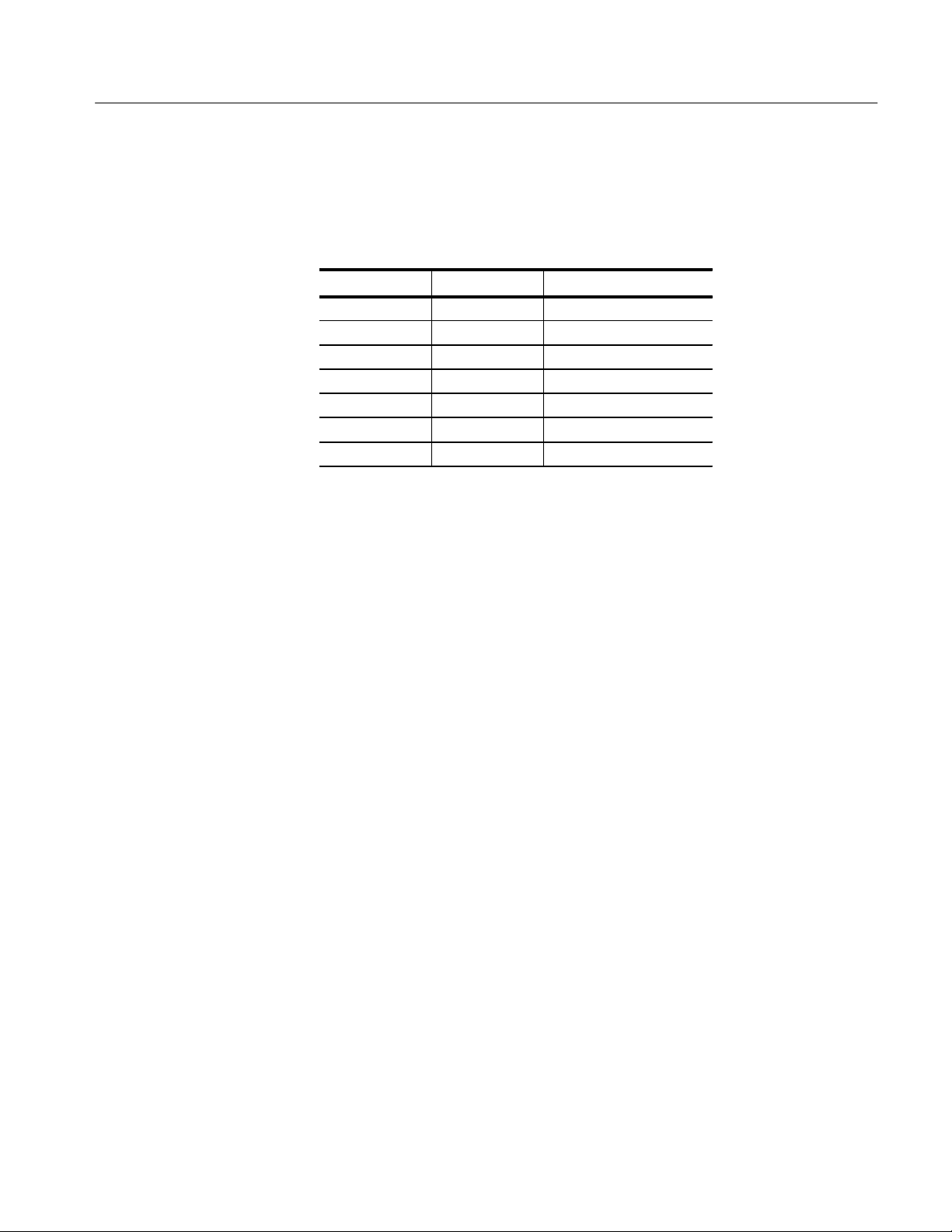
Column Column name Description
1 Component number The component number appears on diagrams and circuit board illustrations, located in the diagrams
section. Assembly numbers are clearly marked on each diagram and circuit board illustration in the
Diagrams section, and on the mechanical exploded views in the Replaceable Mechanical Parts list
section. The component number is obtained by adding the assembly number prefix to the circuit
number (see Component Number illustration following this table).
The electrical parts list is arranged by assemblies in numerical sequence (A1, with its subassemblies
and parts, precedes A2, with its subassemblies and parts).
Chassis-mounted parts have no assembly number prefix, and they are located at the end of the
electrical parts list.
2 Tektronix part number Use this part number when ordering replacement parts from Tektronix.
3 and 4 Serial number Column three indicates the serial number at which the part was first effective. Column four indicates
the serial number at which the part was discontinued. No entry indicates the part is good for all serial
numbers.
5 Name & description An item name is separated from the description by a colon (:). Because of space limitations, an item
name may sometimes appear as incomplete. Use the U.S. Federal Catalog handbook H6-1 for
further item name identification.
6 Mfr. code This indicates the code number of the actual manufacturer of the part.
7 Mfr. part number This indicates the actual manufacturer’s or vendor’s part number.
Abbreviations
Component Number
List of Assemblies
Chassis Parts
Mfr. Code to Manufacturer
Cross Index
Abbreviations conform to American National Standard ANSI Y1.1–1972.
Component Number
A23A2R1234 A23 R1234
Assembly number Circuit Number
Read: Resistor 1234 (of Subassembly 2) of Assembly 23
A2
Subassembly Number
(optional)
A list of assemblies is located at the beginning of the electrical parts list. The
assemblies are listed in numerical order. When a part’s complete component
number is known, this list will identify the assembly in which the part is located.
Chassis-mounted parts and cable assemblies are located at the end of the
Replaceable Electrical Parts List.
The table titled Manufacturers Cross Index shows codes, names, and addresses of
manufacturers or vendors of components listed in the parts list.
5–2
TMS 103 80286 Microprocessor Support Instruction Manual
Page 69

Replaceable Electrical Parts
Manufacturers cross index
Mfr.
code
TK0875 MATSUO ELECTRONICS INC 831 S DOUBLAS ST EL SEGUNDO CA 92641
01295 TEXAS INSTRUMENTS INC
04222 A VX CERAMICS
22526 BERG ELECTRONICS INC (DUPONT) 857 OLD TRAIL RD ETTERS PA 17319
53387 MINNESOTA MINING MFG CO PO BOX 2963 AUSTIN TX 78769–2963
63058 MCKENZIE TECHNOLOGY 910 PAGE AVENUE FREMONT CA 94538
80009 TEKTRONIX INC 14150 SW KARL BRAUN DR
Manufacturer Address City , state, zip code
SEMICONDUCTOR GROUP
DIV OF AVX CORP
13500 N CENTRAL EXPY
PO BOX 655303
19TH AVE SOUTH
P O BOX 867
PO BOX 500
DALLAS TX 75262–5303
MYRTLE BEACH SC 29577
BEAVERT ON OR 97077–0001
Replaceable electrical parts list
Component
number
A1 671–2387–00 CIRCUIT BD ASSY: 80286, PROBE ADAPTER, LASI III 80009 671238700
A2 671–2486–00 CIRCUIT BD ASSY: 80286 PROBE ADAPTER, PLCC68,
A1C245 283–5004–00 CAP, FXD, CERAMIC: MLC; 0.1UF, 10%, 25V, X7R, 1206 04222 12063C104KAT3A
A1C340 283–5004–00 CAP, FXD, CERAMIC: MLC; 0.1UF, 10%, 25V, X7R, 1206 04222 12063C104KAT3A
A1C345 290–5005–00 CAP, FXD, TANT: 47UF, 10%, 10V, 5.8MM X 4.6MM TK0875 267M–1002–476–K
A1C400 283–5004–00 CAP, FXD, CERAMIC: MLC; 0.1UF, 10%, 25V, X7R, 1206 04222 12063C104KAT3A
A1C420 283–5004–00 CAP, FXD, CERAMIC: MLC; 0.1UF, 10%, 25V, X7R, 1206 04222 12063C104KAT3A
A1J130 131–5267–00 CONN, HDR: PCB, MALE, STR, 2 X 40, 0.1 CTR, 0.235 53387 N–2480–6122–TB
A1J300 131–5267–00 CONN, HDR: PCB, MALE, STR, 2 X 40, 0.1 CTR, 0.235 53387 N–2480–6122–TB
A1J310 131–5267–00 CONN, HDR: PCB, MALE, STR, 2 X 40, 0.1 CTR, 0.235 53387 N–2480–6122–TB
A1J350 131–5267–00 CONN, HDR: PCB, MALE, STR, 2 X 40, 0.1 CTR, 0.235 53387 N–2480–6122–TB
A1J530 131–5267–00 CONN, HDR: PCB, MALE, STR, 2 X 40, 0.1 CTR, 0.235 53387 N–2480–6122–TB
A1U410 160–8830–00 IC, DIGITAL: STTL, PLD; PAL, 20R6, 125MHZ, 210MA, PRGM
A1U430 136–0921–00 SOCKET, PGA: PCB, 68 POS, 11 X 11, 0.1 CTR, 0.170 H X 0.183
Tektronix
part number
Serial no.
effective
Serial no.
discont’d
Name & description
SOCKETED;
156–6381–00
TAIL, OPEN CTR, SYMMETRICAL, PAT1132
Mfr.
code
80009 671248600
80009 160–8830–00
63058 PGA 68H101B1–11
Mfr. part number
TMS 103 80286 Microprocessor Support Instruction Manual
5–3
Page 70

Replaceable Electrical Parts
Replaceable electrical parts list (cont.)
Component
number
A2 671–2486–00 CIRCUIT BD ASSY: 80286 PROBE ADAPTER, PLCC68,
A2C1240 290–5005–00 CAP, FXD, TANT: 47UF ,10%, 10V, 5.8MM X 4.6MM TK0875 267M–1002–476–K
A2C1330 283–5004–00 CAP, FXD, CERAMIC: MLC; 0.1UF, 10%, 25V, X7R, 1206 04222 12063C104KAT3A
A2C1400 283–5004–00 CAP, FXD, CERAMIC: MLC; 0.1UF, 10%, 25V, X7R, 1206 04222 12063C104KA T3A
A2C1420 283–5004–00 CAP, FXD, CERAMIC: MLC; 0.1UF, 10%, 25V, X7R, 1206 04222 12063C104KA T3A
A2C1430 283–5004–00 CAP, FXD, CERAMIC: MLC; 0.1UF, 10%, 25V, X7R, 1206 04222 12063C104KA T3A
A2J1100 131–5267–00 CONN, HDR: PCB, MALE, STR, 2 X 40, 0.1 CTR, 0.235 53387 N–2480–6122–TB
A2J1130 131–5267–00 CONN, HDR: PCB, MALE, STR, 2 X 40, 0.1 CTR, 0.235 53387 N–2480–6122–TB
A2J1220 131–5267–00 CONN, HDR: PCB, MALE, STR, 2 X 40, 0.1 CTR, 0.235 53387 N–2480–6122–TB
A2J1350 131–5267–00 CONN, HDR: PCB, MALE, STR, 2 X 40, 0.1 CTR, 0.235 53387 N–2480–6122–TB
A2J1530 131–5267–00 CONN, HDR: PCB, MALE, STR, 2 X 40, 0.1 CTR, 0.235 53387 N–2480–6122–TB
A2P2330 –––– ––– CONN, ADPT: SMD, PLCC; MALE, STR, 68 POS, 0.05 CTR,
A2U1330 –––– ––– SOCKET,PLCC: SMD, 68 POS, 0.05 CTR, 0.200 H, TIN, ACCOM
A2U1420 156–6381–00 IC, DIGITAL: STTL, PLD; PAL, 20R6, 125MHZ, 210MA 01295 TIBPAL20R6–5CFN
A2U1420 160–8830–00 IC, DIGITAL: STTL, PLD; PAL, 20R6, 125MHZ, 210MA, PRGM
Tektronix
part number
Serial no.
effective
Serial no.
discont’d
Name & description
SOCKETED
0.268H, PLCC MALE TOSMD PADS
(SEE RMPL)
0.055–0.095
(SEE RMPL)
156–6381–00
Mfr.
code
80009 671248600
80009 160–8830–00
Mfr. part number
5–4
TMS 103 80286 Microprocessor Support Instruction Manual
Page 71

Replaceable Mechanical Parts
Page 72

Page 73

Replaceable Mechanical Parts
This chapter contains a list of the replaceable mechanical components for the
TMS 103 80286 microprocessor support. Use this list to identify and order
replacement parts.
Parts Ordering Information
Replacement parts are available through your local Tektronix field office or
representative.
Changes to Tektronix products are sometimes made to accommodate improved
components as they become available and to give you the benefit of the latest
improvements. Therefore, when ordering parts, it is important to include the
following information in your order.
H Part number
H Instrument type or model number
H Instrument serial number
H Instrument modification number, if applicable
If you order a part that has been replaced with a different or improved part, your
local Tektronix field office or representative will contact you concerning any
change in part number.
Change information, if any, is located at the rear of this manual.
Using the Replaceable Mechanical Parts List
The tabular information in the Replaceable Mechanical Parts List is arranged for
quick retrieval. Understanding the structure and features of the list will help you
find all of the information you need for ordering replacement parts. The
following table describes the content of each column in the parts list.
TMS 103 80286 Microprocessor Support Instruction Manual
6–1
Page 74

Replaceable Mechanical Parts
Parts list column descriptions
Column Column name Description
1 Figure & index number Items in this section are referenced by figure and index numbers to the exploded view illustrations
that follow.
2 Tektronix part number Use this part number when ordering replacement parts from Tektronix.
3 and 4 Serial number Column three indicates the serial number at which the part was first effective. Column four
indicates the serial number at which the part was discontinued. No entries indicates the part is
good for all serial numbers.
5 Qty This indicates the quantity of parts used.
6 Name & description An item name is separated from the description by a colon (:). Because of space limitations, an
item name may sometimes appear as incomplete. Use the U.S. Federal Catalog handbook H6-1
for further item name identification.
7 Mfr. code This indicates the code of the actual manufacturer of the part.
8 Mfr. part number This indicates the actual manufacturer’s or vendor’s part number.
Abbreviations
Chassis Parts
Mfr. Code to Manufacturer
Cross Index
Abbreviations conform to American National Standard ANSI Y1.1–1972.
Chassis-mounted parts and cable assemblies are located at the end of the
Replaceable Electrical Parts List.
The table titled Manufacturers Cross Index shows codes, names, and addresses of
manufacturers or vendors of components listed in the parts list.
6–2
TMS 103 80286 Microprocessor Support Instruction Manual
Page 75

Replaceable Mechanical Parts
Manufacturers cross index
Mfr.
code
TK2358 EMULATION TECHNOLOGY INC 2368B WALSH A VE, BLDG D SANTA CLARA CA 95051
TK2548 XEROX BUSINESS SERVICES DIV OF XEROX
05276 ITT POMONA ELECTRONICS DIV 1500 E 9TH ST PO BOX 2767 POMONA CA 91766–3835
53387 MINNESOTA MINING MFG CO PO BOX 2963 AUSTIN TX 78769–2963
63058 MCKENZIE TECHNOLOGY 910 PAGE AVENUE FREMONT CA 94538
80009 TEKTRONIX INC 14150 SW KARL BRAUN DR PO BOX 500 BEAVERTON OR 97077–0001
Manufacturer Address City , state, zip code
14181 SW MILLIKAN WA Y BEAVERTON OR 97077
CORPORATION
TMS 103 80286 Microprocessor Support Instruction Manual
6–3
Page 76

Replaceable Mechanical Parts
Replaceable mechanical parts list
Fig. &
index
number
1–0 010–0538–00 1 PROBE ADAPTER: 80286, PGA68, SOCKETED 80009 010053800
1–2 131–5267–00 2 CONN, HDR: PCB, MALE, STR, 2 X 40, 0.1 CTR,
1–3
1–4 671–2387–00 1 CIRCUIT BD ASSY: 80286, PROBE ADAPTER, LASI III 80009 671238700
Tektronix part
number
136–0921–00
Serial no.
effective
Serial no.
discont’d
Qty Name & description
0.235 MLG X 0.110 TAIL, 30GOLD
(SEE A01 REPL J130, J300, J310, J350, J530)
1 SOCKET, PGA: PCB, 68 POS, 11 X 11, 0.1 CTR,
0.170 H X 0.183 TAIL, OPEN CTR, SYMMETRICAL, PAT 1132
(USED WITH 136–1023–00 TO FORM AN LCC–TO–PGA
TEST CLIP)
STANDARD ACCESSORIES
Mfr.
code
63058
Mfr. part number
PGA 68H101B1–11
070–9806–00
070–9803–00 1 MANUAL, TECHNICAL: TLA 700 SERIES MICROPROCESSOR
1–1
1–5
1–6 013–0250–00 1 ADAPTER, TEST: 68 PIN PLCC
1–7 103–0311–00
1–8 136–1023–00 1 SKT, PL–IN ELEK: MICROCKT , 68 CONTACT, LCC (USED
136–0921–00 2
103–0294–00
070–9802–00 1 MANUAL, TECH: BASIC OPS MICROPROCESSOR
1 MANUAL, TECHNICAL: TMS 103, 80286 MICROPROCESSOR
SUPPORT INSTRUCTION MANUAL
SUPPORT INSTALLATION
OPTIONAL ACCESSORIES
SOCKET, PGA: PCB, 68 POS, 11 X 11, 0.1 CTR,
0.170 H X 0.183 TAIL, OPEN CTR, SYMMETRICAL, PAT 1132
(U430)
1 ADAPTER, CONN: 80186/80188 68 PIN LCC TO 68 PIN PGA
(USED WITH 013–0250–00 TO FORM A LCC–TO PGA
TESTCLIP)
(USED WITH 1030311–00 TO FORM A LCC–TO–PGA
TEST CLIP)
ADAPTER, CONN: 68186/8088 68 PIN PGA TO PLCC (USED
2
WITH 013–0250–00 TO FORM AN LCC–TO PGA TESTCLIP)
WITH 136–0921–00 T0 FORM AN LCC–TO PGA TESTCLIP)
SUPPPORT ON DAS/TLA 500 SERIES LOGIC ANAL YZERS
80009 070–9806–00
80009 070–9803–00
63058 AP3–68–PGA–G
TK2358AP3–68–PGA–G
05276
TK2358AC–PGA–PCC–801
53387
80009 070–9802–00
E11886
8
2–0068–05400–08
6–4
TMS 103 80286 Microprocessor Support Instruction Manual
Page 77

Replaceable Mechanical Parts
1
8
2
3
A01
4
5
6
7
Figure 1: PGA probe adapter exploded view
TMS 103 80286 Microprocessor Support Instruction Manual
6–5
Page 78

Replaceable Mechanical Parts
Replaceable mechanical parts list
Fig. &
index
number
2–1 131–5267–00 2 CONN,HDR:PCB,;MALE,STR,2 X 40,0.1 CTR,0.235 MLG X
2–2 671–2486–00 1 CIRCUIT BD ASSY:80286 PROBE ADAPTER,
Tektronix part
number
Serial no.
effective
Serial no.
discont’d
Qty Name & description
0.110 TAIL,30GOLD
(SEE A02 REPL J1100,J1130,J1220,J1350,J1530)
PLCC68,SOCKETED
STANDARD ACCESSORIES
Mfr.
code
80009 671248600
Mfr. part number
070–9806–00 MANUAL,TECH:TMS 103, INSTRUCTION, 80286, DISASSEM-
070–9803–00 1 MANUAL, TECH:TLA 700 SERIES MICROPROCESSOR
070–9802–00 1 MANUAL, TECH:BASIC OPS MICRO SUP ON DAS/TLA 500
BLER
SUPPORT INSTALLATION
OPTIONAL ACCESSORIES
SERIES LOGIC ANALYZERS
1
A02
2
80009 070980600
80009 070–9803–00
80009 070–9802–00
6–6
Figure 2: PLCC probe adapter exploded view
TMS 103 80286 Microprocessor Support Instruction Manual
Page 79

Index
Page 80

Page 81

Index
A
about this manual set, ix
acquiring data, 2–5
Address group
channel assignments, 3–8
display column, 2–8
Alternate Bus Master Cycles, clocking option, 2–2
alternate connections
extra channel probes, 3–14
to other signals, 3–13
B
basic operations, where to find information, ix
bus cycles, displayed cycle types, 2–6
bus timing, 3–12
C
certifications, 3–4
channel assignments
Address group, 3–8
clocks, 3–11
Control group, 3–9
Copr group, 3–10
Data group, 3–9
Intr group, 3–10
Misc group, 3–10
channel groups, 2–1
clock channel assignments, 3–11
clock rate, 1–2
clocking, Custom, 2–1
how data is acquired, 3–12
clocking options
Alternate Bus Master Cycles, 2–2
field names, 2–1
how data is acquired, 3–13
compliances, 3–4
connections
no probe adapter, 1–9
channel probes, 1–10
clock probes, 1–11
other microprocessor signals, 3–13
probe adapter to SUT
PGA, 1–3
PLCC, 1–6
Control Flow display format, 2–9
Control group
channel assignments, 3–9
symbol table, 2–2
Copr group, channel assignments, 3–10
Custom clocking, 2–1
Alternate Bus Master Cycles, 2–2
how data is acquired, 3–12
cycle types, 2–6
D
data
acquiring, 2–5
disassembly formats
Control Flow, 2–9
Hardware, 2–6
Software, 2–9
Subroutine, 2–9
how it is acquired, 3–11
data display , changing, 2–9
Data group
channel assignments, 3–9
display column, 2–8
demonstration system file, 2–13
dimensions
PGA probe adapter, 3–6
PLCC probe adapter, 3–6
disassembled data
cycle type definitions, 2–6
viewing, 2–5
disassembler
definition, ix
logic analyzer configuration, 1–2
setup, 2–1
Disassembly Format Definition overlay, 2–10
Disassembly property page, 2–10
display formats
Control Flow, 2–9
Hardware, 2–6
Software, 2–9
special characters, 2–5
Subroutine, 2–9
E
electrical specifications, 3–1
environmental specifications, 3–3
exception vectors, 2–11
TMS 103 80286 Microprocessor Support Instruction Manual
Index–1
Page 82

Index
H
Hardware display format, 2–6
cycle type definitions, 2–6
I
installing hardware. See connections
Intr group, channel assignments, 3–10
L
leads (podlets). See connections
logic analyzer
configuration for disassembler, 1–2
software compatibility, 1–2
M
manual
conventions, ix
how to use the set, ix
Mark Cycle function, 2–10
Mark Opcode function, 2–10
mark selection
16 bit acquisition, 2–11
8 bit acquisition, 2–11
marking cycles, definition of, 2–10
microprocessor
package types supported, 1–1
specific clocking and how data is acquired, 3–12
Misc group, channel assignments, 3–10
Mnemonic display column, 2–8
P
configuring, 1–3
connecting leads, 1–8
hardware description, 3–1
not using one, 1–9
placing the microprocessor in, 1–5, 1–7, 1–8
probe adapter circuit description, 4–1
Processor Support submenu, 2–10
R
restrictions, 1–2
without a probe adapter, 1–9
S
setups, disassembler, 2–1
signals
active low sign, x
alternate connections, 3–13
extra channel probes, 3–14
Software display format, 2–9
special characters displayed, 2–5
specifications, 3–1
certifications, 3–4
channel assignments, 3–7
compliances, 3–4
electrical, 3–1
environmental, 3–3
mechanical (dimensions), 3–6
Subroutine display format, 2–9
support setup, 2–1
SUT, definition, ix
SUT power, 1–3
symbol table, Control channel group, 2–2
system file, demonstration, 2–13
PGA probe adapter, clearance, dimensions, 3–6
PLCC probe adapter, clearance, dimensions, 3–6
power, SUT, 1–3
probe adapter
alternate connections, 3–13
circuit description, 4–1
clearance, 1–3
adding sockets, 1–5
Index–2
T
terminology, ix
Timestamp display column, 2–8
V
viewing disassembled data, 2–5
TMS 103 80286 Microprocessor Support Instruction Manual
Page 83

Page 84

 Loading...