

Page 1

Instruction Manual
TMS 102
80186 & 80188 Microprocessor Support
070-9805-01
There are no current European directives that
apply to this product. This product provides
cable and test lead connections to a test object of
electronic measuring and test equipment.
Warning
The servicing instructions are for use by
qualified personnel only. To avoid personal
injury, do not perform any servicing unless you
are qualified to do so. Refer to all safety
summaries prior to performing service.
Page 2

Copyright T ektronix, Inc. All rights reserved. Licensed software products are owned by Tektronix or its suppliers and are
protected by United States copyright laws and international treaty provisions.
Use, duplication, or disclosure by the Government is subject to restrictions as set forth in subparagraph (c)(1)(ii) of the
Rights in T echnical Data and Computer Software clause at DFARS 252.227-7013, or subparagraphs (c)(1) and (2) of the
Commercial Computer Software – Restricted Rights clause at F AR 52.227-19, as applicable.
T ektronix products are covered by U.S. and foreign patents, issued and pending. Information in this publication supercedes
that in all previously published material. Specifications and price change privileges reserved.
Printed in the U.S.A.
T ektronix, Inc., P.O. Box 1000, Wilsonville, OR 97070–1000
TEKTRONIX and TEK are registered trademarks of T ektronix, Inc.
Page 3

SOFTWARE WARRANTY
T ektronix warrants that the media on which this software product is furnished and the encoding of the programs on
the media will be free from defects in materials and workmanship for a period of three (3) months from the date of
shipment. If a medium or encoding proves defective during the warranty period, T ektronix will provide a
replacement in exchange for the defective medium. Except as to the media on which this software product is
furnished, this software product is provided “as is” without warranty of any kind, either express or implied.
T ektronix does not warrant that the functions contained in this software product will meet Customer’s
requirements or that the operation of the programs will be uninterrupted or error-free.
In order to obtain service under this warranty, Customer must notify Tektronix of the defect before the expiration
of the warranty period. If T ektronix is unable to provide a replacement that is free from defects in materials and
workmanship within a reasonable time thereafter, Customer may terminate the license for this software product
and return this software product and any associated materials for credit or refund.
THIS WARRANTY IS GIVEN BY TEKTRONIX IN LIEU OF ANY OTHER WARRANTIES, EXPRESS
OR IMPLIED. TEKTRONIX AND ITS VENDORS DISCLAIM ANY IMPLIED WARRANTIES OF
MERCHANTABILITY OR FITNESS FOR A PARTICULAR PURPOSE. TEKTRONIX’
RESPONSIBILITY TO REPLACE DEFECTIVE MEDIA OR REFUND CUSTOMER’S PAYMENT IS
THE SOLE AND EXCLUSIVE REMEDY PROVIDED TO THE CUSTOMER FOR BREACH OF THIS
WARRANTY. TEKTRONIX AND ITS VENDORS WILL NOT BE LIABLE FOR ANY INDIRECT,
SPECIAL, INCIDENTAL, OR CONSEQUENTIAL DAMAGES IRRESPECTIVE OF WHETHER
TEKTRONIX OR THE VENDOR HAS ADVANCE NOTICE OF THE POSSIBILITY OF SUCH
DAMAGES.
Page 4

HARDWARE WARRANTY
T ektronix warrants that the products that it manufactures and sells will be free from defects in materials and
workmanship for a period of one (1) year from the date of shipment. If a product proves defective during this
warranty period, T ektronix, at its option, either will repair the defective product without charge for parts and labor,
or will provide a replacement in exchange for the defective product.
In order to obtain service under this warranty, Customer must notify Tektronix of the defect before the expiration
of the warranty period and make suitable arrangements for the performance of service. Customer shall be
responsible for packaging and shipping the defective product to the service center designated by T ektronix, with
shipping charges prepaid. Tektronix shall pay for the return of the product to Customer if the shipment is to a
location within the country in which the T ektronix service center is located. Customer shall be responsible for
paying all shipping charges, duties, taxes, and any other charges for products returned to any other locations.
This warranty shall not apply to any defect, failure or damage caused by improper use or improper or inadequate
maintenance and care. T ektronix shall not be obligated to furnish service under this warranty a) to repair damage
resulting from attempts by personnel other than T ektronix representatives to install, repair or service the product;
b) to repair damage resulting from improper use or connection to incompatible equipment; c) to repair any
damage or malfunction caused by the use of non-T ektronix supplies; or d) to service a product that has been
modified or integrated with other products when the effect of such modification or integration increases the time
or difficulty of servicing the product.
THIS WARRANTY IS GIVEN BY TEKTRONIX IN LIEU OF ANY OTHER WARRANTIES, EXPRESS
OR IMPLIED. TEKTRONIX AND ITS VENDORS DISCLAIM ANY IMPLIED WARRANTIES OF
MERCHANTABILITY OR FITNESS FOR A PARTICULAR PURPOSE. TEKTRONIX’
RESPONSIBILITY TO REPAIR OR REPLACE DEFECTIVE PRODUCTS IS THE SOLE AND
EXCLUSIVE REMEDY PROVIDED TO THE CUST OMER FOR BREACH OF THIS WARRANTY.
TEKTRONIX AND ITS VENDORS WILL NOT BE LIABLE FOR ANY INDIRECT , SPECIAL,
INCIDENTAL, OR CONSEQUENTIAL DAMAGES IRRESPECTIVE OF WHETHER TEKTRONIX OR
THE VENDOR HAS ADVANCE NOTICE OF THE POSSIBILITY OF SUCH DAMAGES.
Page 5

Table of Contents
Getting Started
Operating Basics
General Safety Summary v. . . . . . . . . . . . . . . . . . . . . . . . . . . . . . . . . . . .
Service Safety Summary vii. . . . . . . . . . . . . . . . . . . . . . . . . . . . . . . . . . . . .
Preface: Microprocessor Support Documentation ix. . . . . . . . . . . . . . . .
Manual Conventions ix. . . . . . . . . . . . . . . . . . . . . . . . . . . . . . . . . . . . . . . . . . . . . .
Logic Analyzer Documentation x. . . . . . . . . . . . . . . . . . . . . . . . . . . . . . . . . . . . . .
Contacting T ektronix x. . . . . . . . . . . . . . . . . . . . . . . . . . . . . . . . . . . . . . . . . . . . . .
Getting Started 1–1. . . . . . . . . . . . . . . . . . . . . . . . . . . . . . . . . . . . . . . . . . . .
Support Description 1–1. . . . . . . . . . . . . . . . . . . . . . . . . . . . . . . . . . . . . . . . . . . . . . .
Logic Analyzer Software Compatibility 1–2. . . . . . . . . . . . . . . . . . . . . . . . . . . . . . .
Logic Analyzer Configuration 1–2. . . . . . . . . . . . . . . . . . . . . . . . . . . . . . . . . . . . . . .
Requirements and Restrictions 1–2. . . . . . . . . . . . . . . . . . . . . . . . . . . . . . . . . . . . . . .
Connecting to a System Under T est 1–3. . . . . . . . . . . . . . . . . . . . . . . . . . . . . . . . . . .
PGA Probe Adapter 1–3. . . . . . . . . . . . . . . . . . . . . . . . . . . . . . . . . . . . . . . . . . .
PLCC Probe Adapter 1–6. . . . . . . . . . . . . . . . . . . . . . . . . . . . . . . . . . . . . . . . . .
Without a Probe Adapter 1–9. . . . . . . . . . . . . . . . . . . . . . . . . . . . . . . . . . . . . . . .
Specifications
Setting Up the Support 2–1. . . . . . . . . . . . . . . . . . . . . . . . . . . . . . . . . . . . . .
Channel Group Definitions 2–1. . . . . . . . . . . . . . . . . . . . . . . . . . . . . . . . . . . . . . . . .
Clocking Options 2–1. . . . . . . . . . . . . . . . . . . . . . . . . . . . . . . . . . . . . . . . . . . . . . . . .
DMA Cycles 2–2. . . . . . . . . . . . . . . . . . . . . . . . . . . . . . . . . . . . . . . . . . . . . . . . .
Symbols 2–2. . . . . . . . . . . . . . . . . . . . . . . . . . . . . . . . . . . . . . . . . . . . . . . . . . . . . . . .
Acquiring and Viewing Disassembled Data 2–5. . . . . . . . . . . . . . . . . . . . .
Acquiring Data 2–5. . . . . . . . . . . . . . . . . . . . . . . . . . . . . . . . . . . . . . . . . . . . . . . . . . .
Viewing Disassembled Data 2–5. . . . . . . . . . . . . . . . . . . . . . . . . . . . . . . . . . . . . . . .
Hardware Display Format 2–6. . . . . . . . . . . . . . . . . . . . . . . . . . . . . . . . . . . . . . .
Software Display Format 2–8. . . . . . . . . . . . . . . . . . . . . . . . . . . . . . . . . . . . . . .
Control Flow Display Format 2–8. . . . . . . . . . . . . . . . . . . . . . . . . . . . . . . . . . . .
Subroutine Display Format 2–8. . . . . . . . . . . . . . . . . . . . . . . . . . . . . . . . . . . . . .
Changing How Data is Displayed 2–8. . . . . . . . . . . . . . . . . . . . . . . . . . . . . . . . . . . .
Marking Cycles 2–9. . . . . . . . . . . . . . . . . . . . . . . . . . . . . . . . . . . . . . . . . . . . . . .
Viewing an Example of Disassembled Data 2–10. . . . . . . . . . . . . . . . . . . . . . . . . . . .
Specifications 3–1. . . . . . . . . . . . . . . . . . . . . . . . . . . . . . . . . . . . . . . . . . . . . .
Probe Adapter Description 3–1. . . . . . . . . . . . . . . . . . . . . . . . . . . . . . . . . . . . . . . . . .
Configuration 3–1. . . . . . . . . . . . . . . . . . . . . . . . . . . . . . . . . . . . . . . . . . . . . . . . . . . .
Specifications 3–1. . . . . . . . . . . . . . . . . . . . . . . . . . . . . . . . . . . . . . . . . . . . . . . . . . . .
Channel Assignments 3–5. . . . . . . . . . . . . . . . . . . . . . . . . . . . . . . . . . . . . . . . . .
How Data is Acquired 3–11. . . . . . . . . . . . . . . . . . . . . . . . . . . . . . . . . . . . . . . . . . . . .
Custom Clocking 3–11. . . . . . . . . . . . . . . . . . . . . . . . . . . . . . . . . . . . . . . . . . . . .
Clocking Options 3–13. . . . . . . . . . . . . . . . . . . . . . . . . . . . . . . . . . . . . . . . . . . . .
Alternate Microprocessor Connections 3–14. . . . . . . . . . . . . . . . . . . . . . . . . . . . . . . .
TMS 102 80186 & 80188 Microprocessor Support Instruction Manual
i
Page 6

Table of Contents
Signals On the Probe Adapter 3–14. . . . . . . . . . . . . . . . . . . . . . . . . . . . . . . . . . . .
Maintenance
Maintenance 4–1. . . . . . . . . . . . . . . . . . . . . . . . . . . . . . . . . . . . . . . . . . . . . . .
Probe Adapter Circuit Description 4–1. . . . . . . . . . . . . . . . . . . . . . . . . . . . . . . . . . . .
Replacing Signal Leads 4–1. . . . . . . . . . . . . . . . . . . . . . . . . . . . . . . . . . . . . . . . . . . .
Replacing Protective Sockets 4–1. . . . . . . . . . . . . . . . . . . . . . . . . . . . . . . . . . . . . . . .
Replaceable Electrical Parts
Replaceable Electrical Parts 5–1. . . . . . . . . . . . . . . . . . . . . . . . . . . . . . . . . .
Parts Ordering Information 5–1. . . . . . . . . . . . . . . . . . . . . . . . . . . . . . . . . . . . . . . . .
Using the Replaceable Electrical Parts List 5–1. . . . . . . . . . . . . . . . . . . . . . . . . . . . .
Replaceable Mechanical Parts
Replaceable Mechanical Parts 6–1. . . . . . . . . . . . . . . . . . . . . . . . . . . . . . . .
Parts Ordering Information 6–1. . . . . . . . . . . . . . . . . . . . . . . . . . . . . . . . . . . . . . . . .
Using the Replaceable Mechanical Parts List 6–1. . . . . . . . . . . . . . . . . . . . . . . . . . .
Index
ii
TMS 102 80186 & 80188 Microprocessor Support Instruction Manual
Page 7

List of Figures
Table of Contents
Figure 1–1: Placing a microprocessor into a PGA probe adapter 1–4. . .
Figure 1–2: Connecting probes to a PGA probe adapter 1–5. . . . . . . . . .
Figure 1–3: Placing a PGA probe adapter onto the SUT 1–6. . . . . . . . . .
Figure 1–4: Placing a microprocessor into a PLCC probe adapter 1–7. .
Figure 1–5: Connecting probes to a PLCC probe adapter 1–8. . . . . . . . .
Figure 1–6: Placing a PLCC probe adapter onto the SUT 1–9. . . . . . . . .
Figure 2–1: Hardware display format 2–7. . . . . . . . . . . . . . . . . . . . . . . . . .
Figure 3–1: Minimum Clearance of the PGA Probe Adapter 3–4. . . . . .
Figure 3–2: Minimum Clearance of the PLCC Probe Adapter 3–5. . . . .
Figure 3–3: 80186/80188 Clocking 3–12. . . . . . . . . . . . . . . . . . . . . . . . . . . . .
Figure 6–1: 80186/80188 PGA probe adapter exploded view 6–5. . . . . . .
Figure 6–2: 80186/80188 PLCC probe adapter exploded view 6–5. . . . . .
TMS 102 80186 & 80188 Microprocessor Support Instruction Manual
iii
Page 8

Table of Contents
List of Tables
Table 1–1: Product support 1–1. . . . . . . . . . . . . . . . . . . . . . . . . . . . . . . . . .
Table 1–2: 80186/80188 signal connections for channel probes 1–10. . . . .
Table 1–3: 80186/80188 signal connections for clock probes 1–11. . . . . . . .
Table 2–1: Control group symbol table definitions 2–2. . . . . . . . . . . . . . .
Table 2–2: Meaning of special characters in the display 2–6. . . . . . . . . .
Table 2–3: Cycle type definitions 2–6. . . . . . . . . . . . . . . . . . . . . . . . . . . . .
Table 2–4: 80186 prefetch cycles 2–9. . . . . . . . . . . . . . . . . . . . . . . . . . . . . .
Table 2–5: 80188 prefetch cycles 2–10. . . . . . . . . . . . . . . . . . . . . . . . . . . . . .
Table 3–1: Electrical specifications 3–2. . . . . . . . . . . . . . . . . . . . . . . . . . . .
Table 3–2: Environmental specification* 3–2. . . . . . . . . . . . . . . . . . . . . . .
Table 3–3: Certifications and compliances 3–3. . . . . . . . . . . . . . . . . . . . . .
Table 3–4: Address group channel assignments 3–6. . . . . . . . . . . . . . . . . .
Table 3–5: Data group channel assignments 3–7. . . . . . . . . . . . . . . . . . . . .
Table 3–6: Control group channel assignments 3–7. . . . . . . . . . . . . . . . . .
Table 3–7: Interrupt group channel assignments 3–8. . . . . . . . . . . . . . . .
Table 3–8: Timer group channel assignments 3–8. . . . . . . . . . . . . . . . . . .
Table 3–9: Chip_Select group channel assignments 3–9. . . . . . . . . . . . . .
Table 3–10: Misc group channel assignments 3–9. . . . . . . . . . . . . . . . . . .
Table 3–11: Async group channel assignments 3–10. . . . . . . . . . . . . . . . . .
Table 3–12: Clock group channel assignments 3–11. . . . . . . . . . . . . . . . . .
iv
TMS 102 80186 & 80188 Microprocessor Support Instruction Manual
Page 9

General Safety Summary
Review the following safety precautions to avoid injury and prevent damage to
this product or any products connected to it. To avoid potential hazards, use this
product only as specified.
Only qualified personnel should perform service procedures.
While using this product, you may need to access other parts of the system. Read
the General Safety Summary in other system manuals for warnings and cautions
related to operating the system.
To Avoid Fire or Personal Injury
Symbols and Terms
Observe All Terminal Ratings. To avoid fire or shock hazard, observe all ratings
and marking on the product. Consult the product manual for further ratings
information before making connections to the product.
Do not apply a potential to any terminal, including the common terminal, that
exceeds the maximum rating of that terminal.
Avoid Exposed Circuitry. Do not touch exposed connections and components
when power is present.
Do Not Operate With Suspected Failures. If you suspect there is damage to this
product, have it inspected by qualified service personnel.
Do Not Operate in Wet/Damp Conditions.
Do Not Operate in an Explosive Atmosphere.
Keep Product Surfaces Clean and Dry .
Provide Proper Ventilation. Refer to the manual’s installation instructions for
details on installing the product so it has proper ventilation.
T erms in this Manual. These terms may appear in this manual:
WARNING. Warning statements identify conditions or practices that could result
in injury or loss of life.
CAUTION. Caution statements identify conditions or practices that could result in
damage to this product or other property.
TMS 102 80186 & 80188 Microprocessor Support Instruction Manual
v
Page 10

General Safety Summary
T erms on the Product. These terms may appear on the product:
DANGER indicates an injury hazard immediately accessible as you read the
marking.
WARNING indicates an injury hazard not immediately accessible as you read the
marking.
CAUTION indicates a hazard to property including the product.
Symbols on the Product. The following symbols may appear on the product:
WARNING
High Voltage
Protective Ground
(Earth) T erminal
CAUTION
Refer to Manual
Double
Insulated
vi
TMS 102 80186 & 80188 Microprocessor Support Instruction Manual
Page 11

Service Safety Summary
Only qualified personnel should perform service procedures. Read this Service
Safety Summary and the General Safety Summary before performing any service
procedures.
Do Not Service Alone. Do not perform internal service or adjustments of this
product unless another person capable of rendering first aid and resuscitation is
present.
Disconnect Power. To avoid electric shock, disconnect the main power by means
of the power cord or, if provided, the power switch.
Use Care When Servicing With Power On. Dangerous voltages or currents may
exist in this product. Disconnect power, remove battery (if applicable), and
disconnect test leads before removing protective panels, soldering, or replacing
components.
To avoid electric shock, do not touch exposed connections.
TMS 102 80186 & 80188 Microprocessor Support Instruction Manual
vii
Page 12

Service Safety
viii
TMS 102 80186 & 80188 Microprocessor Support Instruction Manual
Page 13

Preface: Microprocessor Support Documentation
This instruction manual contains specific information about the TMS 102
80186/80188 microprocessor support and is part of a set of information on how
to operate this product on compatible Tektronix logic analyzers.
If you are familiar with operating microprocessor supports on the logic analyzer
for which the TMS 102 80186/80188 support was purchased, you will probably
only need this instruction manual to set up and run the support.
If you are not familiar with operating microprocessor supports, you will need to
supplement this instruction manual with information on basic operations to set up
and run the support.
Information on basic operations of microprocessor supports is included with each
product. Each logic analyzer has basic information that describes how to perform
tasks common to supports on that platform. This information can be in the form
of online help, an installation manual, or a user manual.
This manual provides detailed information on the following topics:
H Connecting the logic analyzer to the system under test
Manual Conventions
H Setting up the logic analyzer to acquire data from the system under test
H Acquiring and viewing disassembled data
H Using the probe adapter
This manual uses the following conventions:
H The term disassembler refers to the software that disassembles bus cycles
into instruction mnemonics and cycle types.
H The phrase “information on basic operations” refers to online help, an
installation manual, or a basic operations of microprocessor supports user
manual.
H In the information on basic operations, the term XXX or P54C used in field
selections and file names can be replaced with 80186. This is the name of
the microprocessor in field selections and file names you must use to operate
the 80186/80188 support.
H The term system under test (SUT) refers to the microprocessor-based system
from which data will be acquired.
TMS 102 80186 & 80188 Microprocessor Support Instruction Manual
ix
Page 14

Preface: Microprocessor Support Documentation
H The term logic analyzer refers to the Tektronix logic analyzer for which this
product was purchased.
H The term module refers to a 102/136-channel or 96-channel module.
H 80186 refers to all supported variations of the 80186/80188 microprocessor
unless otherwise noted.
H 80186/188 refers to both the 80186 and 80188 microprocessors unless
otherwise noted.
H A tilde (~) following a signal name indicates an active low signal.
Logic Analyzer Documentation
A description of other documentation available for each type of Tektronix logic
analyzer is located in the corresponding module user manual. The manual set
provides the information necessary to install, operate, maintain, and service the
logic analyzer and associated products.
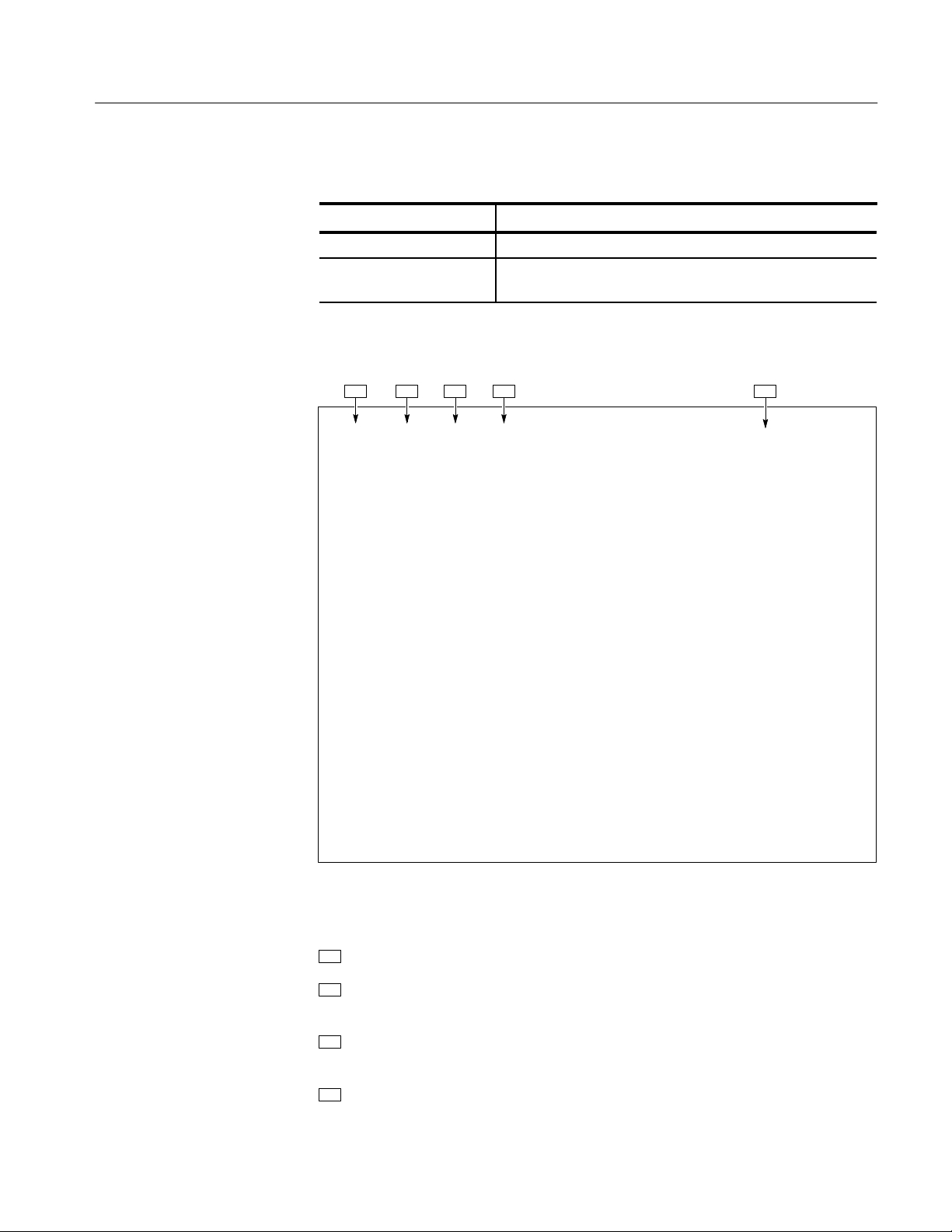
Contacting Tektronix
Product
Support
Service
Support
For other
information
To write us Tektronix, Inc.
For application-oriented questions about a Tektronix measurement product, call toll free in North America:
1-800-TEK-WIDE (1-800-835-9433 ext. 2440)
6:00 a.m. – 5:00 p.m. Pacific time
Or, contact us by e-mail:
tm_app_supp@tek.com
For product support outside of North America, contact your
local Tektronix distributor or sales office.
Contact your local Tektronix distributor or sales office. Or, visit
our web site for a listing of worldwide service locations.
http://www.tek.com
In North America:
1-800-TEK-WIDE (1-800-835-9433)
An operator will direct your call.
P.O. Box 1000
Wilsonville, OR 97070-1000
x
TMS 102 80186 & 80188 Microprocessor Support Instruction Manual
Page 15

Getting Started
Page 16

Page 17
Getting Started
Support Description
This chapter provides information on the following topics:
H A description of the TMS 102 microprocessor support
H Logic analyzer software compatibility
H Your system under test requirements
H Support restrictions
H How to connect to the system under test (SUT)
The TMS 102 microprocessor support disassembles data from systems that are
based on the Intel 80186/80188 microprocessor. This support also disassembles
8087 floating point coprocessor instructions. The support runs on a compatible
Tektronix logic analyzer equipped with a 102/136-channel module or a 96-channel module.
Refer to information on basic operations to determine how many modules and
probes your logic analyzer needs to meet the minimum channel requirements for
the TMS 102 microprocessor support.
Table 1–1 shows the microprocessors and packages from which the TMS 102
support can acquire and disassemble data.
T able 1–1: Product support
Microprocessor Package Number of pins
80186 PGA, PLCC 68
80188 PGA, PLCC 68
A complete list of standard and optional accessories is provided at the end of the
parts list in the Replaceable Mechanical Parts chapter.
A complete list of standard and optional accessories is provided at the end of the
parts list in the Replaceable Parts chapter.
TMS 102 80186 & 80188 Microprocessor Support Instruction Manual
1–1
Page 18

Getting Started
To use this support efficiently, you need to have the items listed in the information on basic operations as well as the 80186/80188 Microprocessor User’s
Manual, Intel.
Information on basic operations also contains a general description of supports.
Logic Analyzer Software Compatibility
The label on the microprocessor support floppy disk states which version of logic
analyzer software the support is compatible with.
Logic Analyzer Configuration
To use the 80186/80188 support, the Tektronix logic analyzer must be equipped
with either a 102/136-channel module, or a 96-channel module at a minimum.
The module must be equipped with enough probes to acquire clock and channel
data from signals in your 80186/80188-based system.
Refer to information on basic operations to determine how many modules and
probes the logic analyzer needs to meet the channel requirements.
Requirements and Restrictions
You should review the general requirements and restrictions of microprocessor
supports in the information on basic operations as they pertain to your SUT.
You should also review electrical, environmental, and mechanical specifications
in the Specifications chapter in this manual as they pertain to your system under
test, as well as the following descriptions of other 80186/80188 support
requirements and restrictions.
System Clock Rate. The microprocessor support product supports the
80186/80188 microprocessor at speeds of up to 20 MHz
1
.
1–2
1
Specification at time of printing. Contact your logic analyzer sales representative for
current information on the fastest devices supported.
TMS 102 80186 & 80188 Microprocessor Support Instruction Manual
Page 19
Connecting to a System Under Test
Before you connect to the SUT, you must connect the probes to the module.
Your SUT must also have a minimum amount of clear space surrounding the
microprocessor to accommodate the probe adapter. Refer to the Specifications
chapter in this manual for the required clearances.
The channel and clock probes shown in this chapter are for a 102/136-channel
module. The probes will look different if you are using a 96-channel module.
The general requirements and restrictions of microprocessor supports in the
information on basic operations shows the vertical dimensions of a channel or
clock probe connected to square pins on a circuit board.
Getting Started
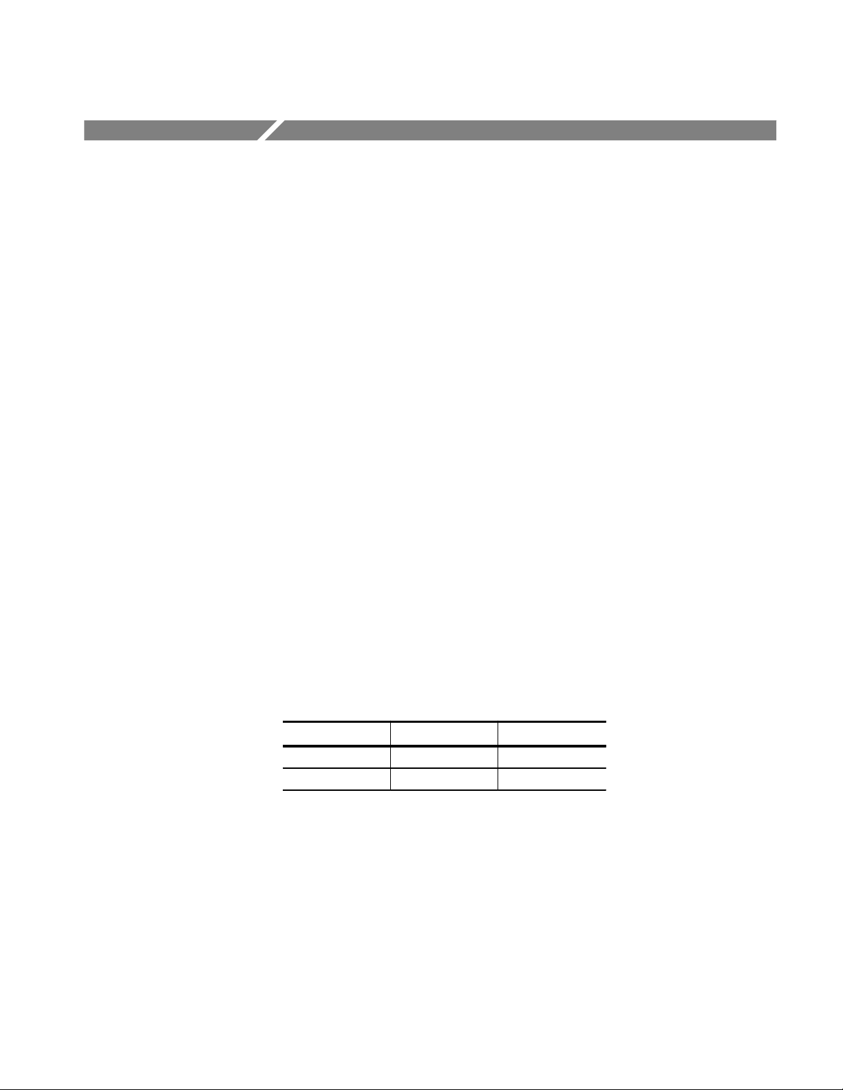
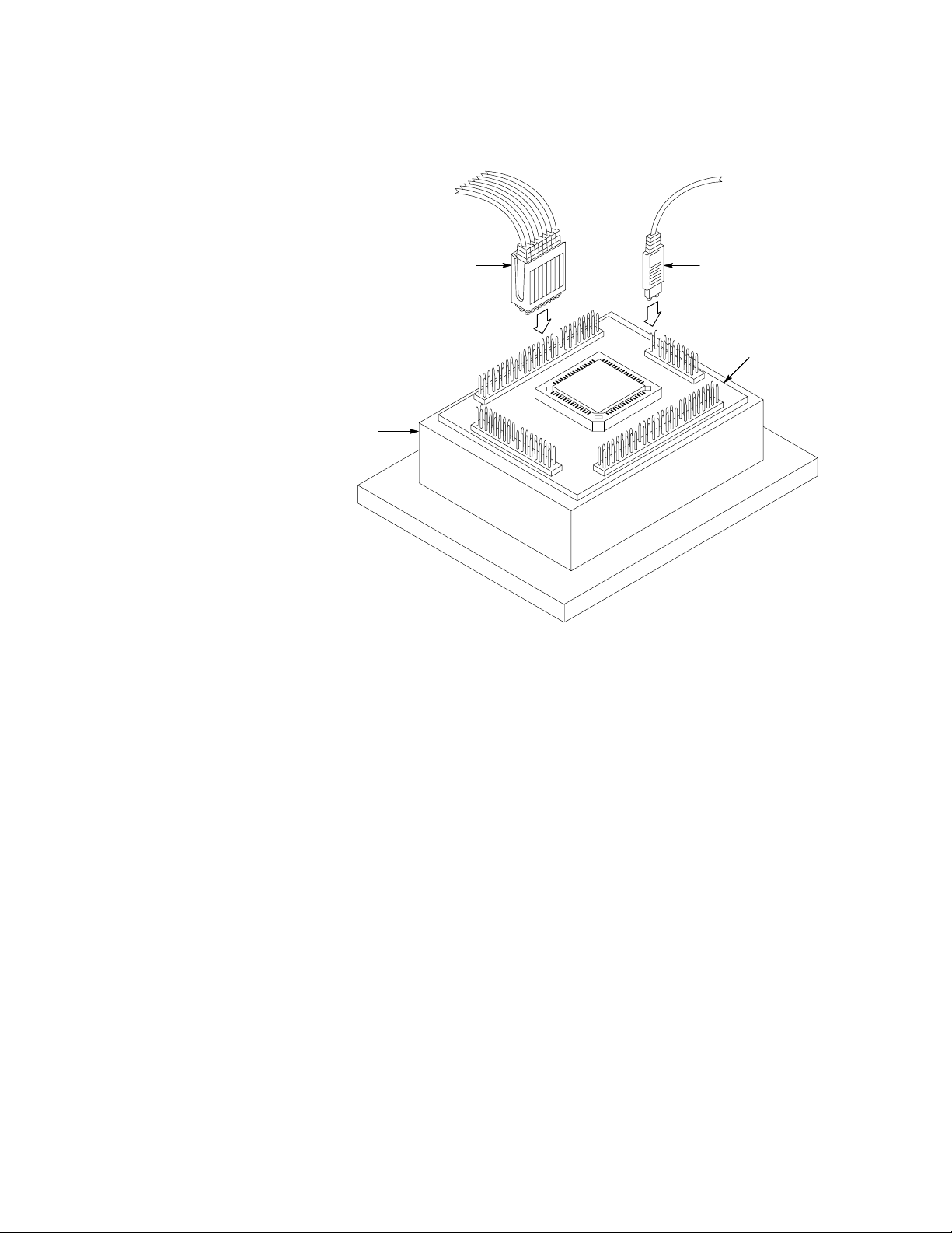
PGA Probe Adapter
To connect the logic analyzer to a SUT using a PGA probe adapter, follow these
steps:
1. Turn off power to your SUT. It is not necessary to turn off power to the logic
analyzer.
CAUTION. Static discharge can damage the microprocessor, the probe adapter,
the probes, or the module. To prevent static damage, handle all of the above only
in a static-free environment.
Always wear a grounding wrist strap or similar device while handling the
microprocessor and probe adapter.
2. To discharge your stored static electricity, touch the ground connector located
on the back of the logic analyzer. Then, touch any of the ground pins of the
probe adapter to discharge stored static electricity from the probe adapter.
3. Place the probe adapter onto the antistatic shipping foam to support the probe
as shown in Figure 1–1. This prevents the circuit board from flexing and the
socket pins from bending.
4. Remove the microprocessor from your SUT.
5. Line up the pin 1 indicator on the probe adapter board with the pin 1
indicator on the microprocessor.
CAUTION. Failure to correctly place the microprocessor into the probe adapter
might permanently damage the microprocessor once power is applied.
6. Place the microprocessor into the probe adapter as shown in Figure 1–1.
TMS 102 80186 & 80188 Microprocessor Support Instruction Manual
1–3
Page 20
Getting Started
Microprocessor
Probe adapter
Foam
Figure 1–1: Placing a microprocessor into a PGA probe adapter
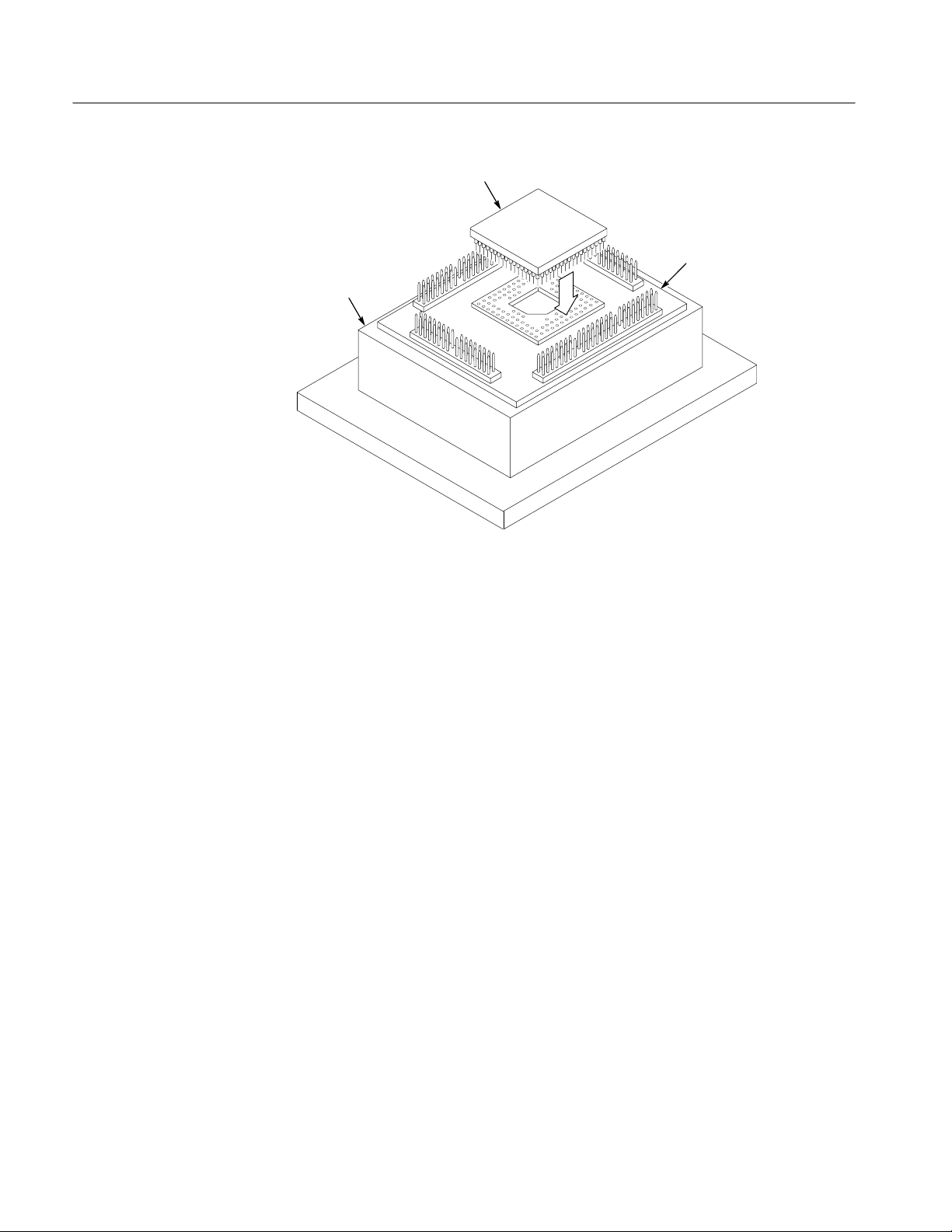
7. Connect the channel and clock probes to the probe adapter as shown in
Figure 1–2. Match the channel groups and numbers on the probe labels to the
corresponding pins on the probe adapter. Match the ground pins on the
probes to the corresponding pins on the probe adapter.
1–4
TMS 102 80186 & 80188 Microprocessor Support Instruction Manual
Page 21

Getting Started
Channel probe
Hold the channel probes by the podlet
holder when connecting them to the
probe adapter. Do not hold them by
the cables or necks of the podlets.
Foam
Figure 1–2: Connecting probes to a PGA probe adapter
Clock probe
Probe adapter
8. Line up the pin 1 indicator on the probe adapter board with the pin 1
indicator on your SUT.
9. Place the probe adapter onto the SUT as shown in Figure 1–3.
NOTE. You might need to stack one or more replacement sockets between the SUT
and the probe adapter to provide sufficient vertical clearance from adjacent
components. However, keep in mind that this might increase loading, which can
reduce the electrical performance of your probe adapter.
TMS 102 80186 & 80188 Microprocessor Support Instruction Manual
1–5
Page 22

Getting Started
SUT socket
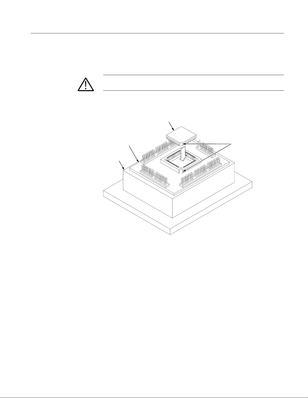
PLCC Probe Adapter
Figure 1–3: Placing a PGA probe adapter onto the SUT
To connect the logic analyzer to a SUT using a PLCC probe adapter, follow these
steps:
1. Turn off power to your SUT. It is not necessary to turn off the logic analyzer.
CAUTION. Static discharge can damage the microprocessor, the probe adapter,
the probes, or the module. To prevent static damage, handle all of the above only
in a static-free environment.
Always wear a grounding wrist strap or similar device while handling the
microprocessor and probe adapter.
2. To discharge your stored static electricity, touch the ground connector located
on the back of the logic analyzer. Then, touch any of the ground pins of the
probe adapter to discharge stored static electricity from the probe adapter.
3. Place the probe adapter onto the antistatic shipping foam to support the probe
as shown in Figure 1–4. This prevents the circuit board from flexing.
4. Remove the microprocessor from your SUT.
1–6
TMS 102 80186 & 80188 Microprocessor Support Instruction Manual
Page 23
Getting Started
5. Line up the pin 1 indicator on the microprocessor with pin 1 of the PLCC
socket on the probe adapter.
CAUTION. Failure to correctly place the microprocessor into the probe adapter
might permanently damage all electrical components once power is applied.
6. Place the microprocessor into the probe adapter as shown in Figure 1–4.
Microprocessor
Probe adapter
Foam
Bevel at both corners
Figure 1–4: Placing a microprocessor into a PLCC probe adapter
7. Connect the channel and clock probes to the probe adapter as shown in
Figure 1–5. Match the channel groups and numbers on the probe labels to the
corresponding pins on the probe adapter. Match the ground pins on the
probes to the corresponding pins on the probe adapter.
TMS 102 80186 & 80188 Microprocessor Support Instruction Manual
1–7
Page 24
Getting Started
Channel probe
Hold the channel probes by the podlet
holder when connecting them to the
probe adapter. Do not hold them by
the cables or necks of the podlets.
Foam
Figure 1–5: Connecting probes to a PLCC probe adapter
Clock probe
Probe adapter
8. Place the probe adapter onto the SUT as shown in Figure 1–6.
1–8
TMS 102 80186 & 80188 Microprocessor Support Instruction Manual
Page 25

Bevel at both
corners
Getting Started
SUT socket
Without a Probe Adapter
Figure 1–6: Placing a PLCC probe adapter onto the SUT
You can use channel probes, clock probes, and leadsets with a commercial test
clip (or adapter) to make connections between the logic analyzer and your SUT.
To connect the probes to 80186/80188 signals in the SUT using a test clip, follow
these steps:
1. Turn off power to your SUT. It is not necessary to turn off power to the logic
analyzer.
CAUTION. Static discharge can damage the microprocessor, the probes, or the
module. To prevent static damage, handle all of the above only in a static-free
environment.
Always wear a grounding wrist strap or similar device while handling the
microprocessor.
2. To discharge your stored static electricity, touch the ground connector located
on the back of the logic analyzer. If you are using a test clip, touch any of the
ground pins on the clip to discharge stored static electricity from it.
TMS 102 80186 & 80188 Microprocessor Support Instruction Manual
1–9
Page 26
Getting Started
CAUTION. Failure to place the SUT on a horizontal surface before connecting the
test clip might permanently damage the pins on the microprocessor.
3. Place the SUT on a horizontal static-free surface.
4. Use Table 1–2 to connect the channel probes to 80186/80188 signal pins on
the test clip or in the SUT.
Use leadsets to connect at least one ground lead from each channel probe and
the ground lead from each clock probe to ground pins on your test clip.
T able 1–2: 80186/80188 signal connections for channel probes
Section:channel 80186/80188 signal Section:channel 80186/80188 signal
A3:7 UCS~* D3:7 CLKOUT_B*
A3:6 LCS~* D3:6 PCS6~*
A3:5 TMR1OUT* D3:5 PCS5~*
A3:4 TMR0OUT* D3:4 PCS4~*
A3:3 TMR1IN* D3:3 PCS3~*
A3:2 TMR0IN* D3:2 PCS2~*
A3:1 DRQ1* D3:1 PCS1~*
A3:0 DRQ0* D3:0 PCS0~*
A2:7 DT_R~* D2:7 Not connected
A2:6 DEN~* D2:6 Not connected
A2:5 HOLD* D2:5 Not connected
A2:4 BHE~ D2:4 S7*
A2:3 A19/S6 D2:3 S6
A2:2 A18/S5 D2:2 S5*
A2:1 A17/S4 D2:1 S4*
A2:0 A16/S3 D2:0 S3*
A1:7 AD15 D1:7 Not connected
A1:6 AD14 D1:6 Not connected
A1:5 AD13 D1:5 Not connected
A1:4 AD12 D1:4 Not connected
A1:3 AD1 1 D1:3 Not connected
A1:2 AD10 D1:2 Not connected
A1:1 AD9 D1:1 Not connected
A1:0 AD8 D1:0 Not connected
A0:7 AD7 D0:7 Not connected
A0:6 AD6 D0:6 Not connected
1–10
TMS 102 80186 & 80188 Microprocessor Support Instruction Manual
Page 27
Getting Started
T able 1–2: 80186/80188 signal connections for channel probes (cont.)
Section:channel 80186/80188 signalSection:channel80186/80188 signal
A0:5 AD5 D0:5 Not connected
A0:4 AD4 D0:4 Not connected
A0:3 AD3 D0:3 Not connected
A0:2 AD2 D0:2 Not connected
A0:1 AD1 D0:1 Not connected
A0:0 AD0 D0:0 Not connected
C3:7 INT3* C2:7 TEST~*
C3:6 INT2* C2:6 NMI*
C3:5 INT1* C2:5 LOCK~
C3:4 INT0* C2:4 S2~
C3:3 MCS3~* C2:3 S1~
C3:2 MCS2~* C2:2 S0~
C3:1 MCS1~* C2:1 HLDA
C3:0 MCS0~* C2:0 RESET
C1:7 Not connected C0:7 Not connected
C1:6 Not connected C0:6 Not connected
C1:5 Not connected C0:5 Not connected
C1:4 Not connected C0:4 SRDY*
C1:3 Not connected C0:3 ARDY*
C1:2 Not connected C0:2 RD~*
C1:1 Not connected C0:1 WR~*
C1:0 Not connected C0:0 ALE~*
* Signal not required for disassembly.
Table 1–3 shows the clock probes and the 80186/80188 signal to which they
must connect for disassembly to be correct.
T able 1–3: 80186/80188 signal connections for clock probes
Section:channel 80186/80188 signal
CK:3 CLKOUT
CK:2 STATUS
CK:1 Not connected
CK:0 Not connected
TMS 102 80186 & 80188 Microprocessor Support Instruction Manual
1–11
Page 28

Getting Started
5. Align pin 1 or A1 of your test clip with the corresponding pin 1 or A1 of the
80186/80188 microprocessor in your SUT and attach the clip to the
microprocessor.
6. Use the channel assignment tables in the Specifications chapter to connect
channel and clock probes to your test clip.
7. Use the channel assignment tables in the Specifications chapter to connect
channel and clock probes to the module probe cables.
8. Connect at least one ground podlet (lead) from each channel probe and the
ground from each clock probe to ground pins on your test clip.
9. Align pin 1 or A1 of your test clip with the corresponding pin 1 or A1 of the
microprocessor in your SUT and attach it to the microprocessor.
1–12
TMS 102 80186 & 80188 Microprocessor Support Instruction Manual
Page 29

Operating Basics
Page 30

Page 31

Setting Up the Support
This section provides information on how to set up the support. Information
covers the following topics:
H Channel group definitions
H Clocking options
H Symbol table files
Remember that the information in this section is specific to the operations and
functions of the TMS 102 80186/80188 support on any Tektronix logic analyzer
for which it can be purchased. Information on basic operations describes general
tasks and functions.
Before you acquire and disassemble data, you need to load the support and
specify setups for clocking and triggering as described in the information on
basic operations. The support provides default values for each of these setups,
but you can change them as needed.
Channel Group Definitions
Clocking Options
The disassembler software automatically defines channel groups for the support.
The channel groups for the 80186/80188 support are Address, Data, Control, Intr,
Timers, Chip_Sel, Async, and Misc. If you want to know which signal is in
which group, refer to the channel assignment tables beginning on page 3–5.
The TMS 102 support offers a microprocessor-specific clocking mode for the
80186/80188 microprocessor. This clocking mode is the default selection
whenever you load the 80186 support.
A description of how cycles are sampled by the module using the support and
probe adapter is found in the Specifications chapter.
Disassembly will not be correct with the Internal or External clocking modes.
Information on basic operations describes how to use these clock selections for
general purpose analysis.
The clocking option for the TMS 102 support is: DMA Cycles.
TMS 102 80186 & 80188 Microprocessor Support Instruction Manual
2–1
Page 32
Setting Up the Support
Symbols
DMA Cycles
A DMA cycle is defined as the cycle in which the 80186/80188 microprocessor
gives up the bus to an alternate device (a DMA device or another
microprocessor). These types of cycles are acquired when you select Included.
The TMS 102 support supplies two symbol table files. The 80186_Ctrl and
80188_Ctrl files replace specific Control channel group values with symbolic
values when Symbolic is the radix for the channel group.
Table 2–1 shows the name, bit pattern, and meaning for the symbols in the files
80186_Ctrl and 80188_Ctrl Control channel group symbol tables.
T able 2–1: Control group symbol table definitions
Control group value
LOCK~ S2~
S6 S1~
Symbol
RESET
DMA_RDINT
DMA_WRINT
DMA_INT
DMA_RDEXT
DMA_WREXT
DMA_EXT
MEM_READ
MEM_WRITE
I/O_READ
I/O_WRITE
FETCH
HAL T
INT_ACK
LKD_M_RD
LKD_M_WR
LKD_IO_RD
LKD_IO_WR
READ
RESET S0~
HLDA BHE~
Meaning
RESET signal asserted
An internal DMA read
An internal DMA write
An internal DMA
An external DMA read
An external DMA write
An external DMA
Data read cycle (nonopcode fetch)
Any memory write
Read from I/O space
Write to I/O space
Code read (opcode fetch)
Processor halted
Responding to an interrupt
Locked memory read cycle (nonop-
code fetch)
Locked memory write cycle
Locked read from I/O space
Locked write to I/O space
Any memory or I/O read cycle except
an Opcode Fetch or Int Ack cycle
2–2
TMS 102 80186 & 80188 Microprocessor Support Instruction Manual
Page 33
Setting Up the Support
T able 2–1: Control group symbol table definitions (cont.)
Control group value
LOCK~ S2~
S6 S1~
Symbol Meaning
WRITE
LOCKED
RESET S0~
HLDA BHE~
Any memory or I/O write
Inseparable back-to-back cycles
Information on basic operations describes how to use symbolic values for
triggering and for displaying other channel groups symbolically, such as the
Address channel group.
TMS 102 80186 & 80188 Microprocessor Support Instruction Manual
2–3
Page 34

Setting Up the Support
2–4
TMS 102 80186 & 80188 Microprocessor Support Instruction Manual
Page 35

Acquiring and Viewing Disassembled Data
This section describes how to acquire data and view it disassembled. Information
covers the following topics:
H Acquiring data
H Viewing disassembled data in various display formats
H Cycle type labels
H How to change the way data is displayed
H How to change disassembled cycles with the mark cycles function
Acquiring Data
Once you load the 80186/80188 support, choose a clocking mode and specify the
trigger, you are ready to acquire and disassemble
If you have any problems acquiring data, refer to information on basic operations
in your online help or Appendix A: Error Messages and Disassembly Problems in
the basic operations user manual, whichever is available.
data.
Viewing Disassembled Data
You can view disassembled data in four different display formats: Hardware,
Software, Control Flow, and Subroutine. The information on basic operations
describes how to select the disassembly display formats.
NOTE. Selections in the Disassembly property page for the 102/136-channel
module, or in the Disassembly Format Definition overlay for the 96-channel
module must be set correctly for your acquired data to be disassembled correctly.
Refer to Changing How Data is Displayed on page 2–8.
The default display format shows the Address, Data, and Control channel group
values for each sample of acquired data.
The disassembler displays special characters and strings in the instruction
mnemonics to indicate significant events. Table 2–2 shows these special
characters and strings, and gives a definition of what they represent.
TMS 102 80186 & 80188 Microprocessor Support Instruction Manual
2–5
Page 36
Acquiring and Viewing Disassembled Data
T able 2–2: Meaning of special characters in the display
Character or string displayed Meaning
m or >> The instruction was manually marked
**** Indicates there is insufficient data available for complete
# Indicates an immediate value
* ILLEGAL INSTRUCTION * Decoded as an illegal instruction
disassembly of the instruction; the number of asterisks will
indicate the width of the data that is unavailable. Each two
asterisks represent a byte.
Hardware Display Format
In Hardware display format, the disassembler displays certain cycle type labels in
parentheses. Table 2–3 shows these cycle type labels and gives a definition of the
cycle they represent. Reads to interrupt and exception vectors will be labeled
with the vector name.
T able 2–3: Cycle type definitions
Cycle type Definition
( RESET ) The RESET signal is asserted
( DMA RDINT ) An internal direct memory access read cycle
( DMA WRINT ) An internal direct memory access write cycle
( DMA RDEXT ) An external direct memory access read cycle
( DMA WREXT ) An external direct memory access write cycle
( HALT ) The processor is halted
( INT ACK ) An interrupt acknowledge cycle
( I/O READ ) A read from I/O space
( I/O WRITE ) A write to I/O space
( MEM READ ) A read from memory that is not an opcode fetch
( MEM WRITE ) Any write to memory
2–6
( LOCKED MEM READ ) A locked read from memory that is not an opcode fetch
( LOCKED MEM WRITE ) A locked write to memeory
( LOCKED I/O READ ) A locked read from I/O space
( LOCKED I/O WRITE ) A locked write to I/O space
( FLUSH ) A fetch cycle computed by the disassembler to be an opcode
flush
( EXTENSION ) A fetch cycle computed by the disassembler to be an opcode
extension
TMS 102 80186 & 80188 Microprocessor Support Instruction Manual
Page 37
Acquiring and Viewing Disassembled Data
T able 2–3: Cycle type definitions (Cont.)
Cycle type Definition
( REFRESH ) A memory refresh cycle, computed by the disassembler
( UNKNOWN ) The combination of bits in the Control channel group is either
unexpected or unrecoginzed.
Figure 2–1 shows an example of the Hardware display.
1 2 3 4 5
Sample Address Data Mnemonics Control T>
-------------------------------------------------------------------------------T 0 FFFF0----00EA--(-RESET-LOCATION-)------------------------FETCH--------
FFFF0 00EA JMP FFC00 FETCH
1 FFFF2 C000 ( EXTENSION ) FETCH >
2 FFFF4 00FF ( EXTENSION ) FETCH >
3 FFFF6 FFFF ( FLUSH ) FETCH >
4 FFC00 38B8 MOV AX,#FE38 FETCH >
5 FFC03 BAFE MOV DX,#FFA0 FETCH >
6 FFC04 FFA0 ( EXTENSION ) FETCH >
7 FFC06 B8EF OUTW DX,AX FETCH >
FFC07 B8EF MOV AX,#007A FETCH
8 FFC08 007A ( EXTENSION ) FETCH >
9 0FFA0 FE38 ( I/O WRITE ) I/O_WRITE >
10 FFC0A A2BA MOV DX,#FFA2 FETCH >
11 FFC0D EFFF OUTW DX,AX FETCH >
12 FFC0E BAB8 MOV AX,#81BA FETCH >
13 FFC11 BA81 MOV DX,#FFA8 FETCH >
14 0FFA2 007A ( I/O WRITE ) I/O_WRITE >
15 FFC12 FFA8 ( EXTENSION ) FETCH >
16 FFC14 B8EF OUTW DX,AX FETCH >
FFC15 B8EF MOV AX,#01FA FETCH
17 FFC16 01FA ( EXTENSION ) FETCH >
18 0FFA8 81BA ( I/O WRITE ) I/O_WRITE >
________________________________________________________________________________
Figure 2–1: Hardware display format
1
Sample Column. Lists the memory locations for the acquired data.
2
Address Group. Lists data from channels connected to the 80186/80188
Address bus.
3
Data Group. Lists data from channels connected to the 80186/80188 Data
bus.
4
Mnemonic Column. Lists the disassembled instructions and cycle types.
TMS 102 80186 & 80188 Microprocessor Support Instruction Manual
2–7
Page 38

Acquiring and Viewing Disassembled Data
5
Control Group. Lists data from channels connected to the 80186/80188
control bus.
Software Display Format
Control Flow Display
Format
The Software display format shows only the first fetch of executed instructions.
Flushed cycles and extensions are not shown, even though they are part of the
executed instruction. Read extensions will be used to disassemble the instruction,
but will not be displayed as a separate cycle in the Software display format. Data
reads and writes are not displayed.
The Control Flow display format shows only the first fetch of instructions that
change the flow of control.
Instructions that generate a change in the flow of control in the 80186/80188
microprocessor are as follows:
BOUND JE JNO
CALL JL JNS
DIV JLE JO
IDIV JMP JP
INTO JNB JS
INTX JNBE LOOP
IRET JNE LOOPNZ
JB JNL LOOPZ
JCXZ JNLE RET
Subroutine Display
Format
The Subroutine display format shows the first fetch of subroutine calls and return
instructions. Instructions that generate a subroutine call or a return in the
80186/80188 microprocessor are as follows:
BOUND IDIV IRET
DIV INTO RET
CALL INTX
Changing How Data is Displayed
There are fields and features that allow you to further modify displayed data to
suit your needs. You can make selections unique to the 80186/80188 support to
do the following tasks:
H Change how data is displayed across all display formats
H Change the interpretation of disassembled cycles
H Display exception vectors
2–8
TMS 102 80186 & 80188 Microprocessor Support Instruction Manual
Page 39
Acquiring and Viewing Disassembled Data
There are no new fields for this support product. Refer to the information on
basic operations for discriptions of common fields.
Marking Cycles
The disassembler has a Mark Opcode function that allows you to change the
interpretation of a cycle type. Using this function, you can select a cycle and
change it to one of the following cycle types:
H Opcode (the first word of an instruction)
H Extension (a subsequent word of an instruction)
H Flush (an opcode or extension that is fetched but not executed)
H Anything (any valid opcode, extension or flush)
Table 2–4 shows the selections for the 80186 microprocessor.
T able 2–4: 80186 prefetch cycles
Program fetch cycle Description
Opcode The one-byte cycle will be disassembled as the beginning
of an instruction.
Extension The one-byte cycle is treated as an extension of the
previous instruction.
Flush The one-byte cycle is not disassembled.
Any opcode The low byte of the cycle will be disassembled as the
beginning of an instruction. The high byte is not marked.
Opcode extension The low byte of the cycle is treated as an instruction
extension. The high byte is not marked.
Opcode flush The low byte of the cycle is not disassembled and the high
byte of the cycle is not marked.
Extension-extension The low byte and the high byte are treated as extensions of
the previous instruction.
Flush-flush The cycle is not disassembled.
Undo marks on this cycle Marks are removed from the cycle and the disassembly
reverts to the premark state.
TMS 102 80186 & 80188 Microprocessor Support Instruction Manual
2–9
Page 40
Acquiring and Viewing Disassembled Data
Table 2–5 shows the selections for the 80188 microprocessor.
T able 2–5: 80188 prefetch cycles
Program fetch cycle Description
Opcode The cycle will be disassembled as the beginning of an
Extension The cycle is treated as an extension of the previous
Flush The cycle is not disassembled.
Undo marks on this cycle Marks are removed from the cycle and the disassembly
Information on basic operations contains more details on marking cycles.
instruction.
instruction.
reverts to the premark state.
Viewing an Example of Disassembled Data
A demonstration system file (or demonstration reference memory) is provided so
you can see an example of how your 80186/80188 microprocessor bus cycles and
instruction mnemonics look when they are disassembled. Viewing the system file
is not a requirement for preparing the module for use and you can view it without
connecting the logic analyzer to your SUT.
Information on basic operations describes how to view the file.
2–10
TMS 102 80186 & 80188 Microprocessor Support Instruction Manual
Page 41

Specifications
Page 42

Page 43

Specifications
This chapter contains the following information:
H Probe adapter description
H Specification tables
H Dimensions of the probe adapter
H Channel assignment tables
H Description of how the module acquires 80186/80188 signals
H List of other accessible microprocessor signals and extra acquisition channels
Probe Adapter Description
The probe adapter is nonintrusive hardware that allows the logic analyzer to
acquire data from a microprocessor in its own operating environment with little
effect, if any, on that system. Information on basic operations contains a figure
showing the logic analyzer connected to a typical probe adapter. Refer to that
figure while reading the following description.
Configuration
Specifications
The probe adapter consists of a circuit board and a socket for a 80186/80188
microprocessor. The probe adapter connects to the microprocessor in the SUT.
Signals from the microprocessor-based system flow from the probe adapter to the
channel groups and through the probe signal leads to the module.
All circuitry on the probe adapter is powered from the SUT.
The PGA probe adapter accommodates the Intel 80186/80188 microprocessor in
a 68-pin PGA package. The PLCC probe adapter accommodates the Intel
80186/80188 microprocessor in a 68-pin PLCC package.
The probe adatper does not require any configuration.
These specifications are for a probe adapter connected between a compatible
Tektronix logic analyzer and a SUT. Table 3–1 shows the electrical requirements
the SUT must produce for the support to acquire correct data.
TMS 102 80186 & 80188 Microprocessor Support Instruction Manual
3–1
Page 44

Specifications
In Table 3–1, for the 102/136-channel module, one podlet load is 20 k in
parallel with 2 pF. For the 96-channel module, one podlet load is 100 k in
parallel with 10 pF.
T able 3–1: Electrical specifications
Characteristics Requirements
SUT DC power requirements
Voltage 4.75-5.25 VDC
Current I max (calculated) 210 mA
I typ (measured) 160 mA
SUT clock
Clock rate Min. DC
Max. 20MHz
Minimum setup time required
Address, Data 5 ns
HLDA 6.5 ns
Relative to CLK rising edge:
S0~-S2~ inactive to active
Relative to CLK falling edge:
S0~-S2~ active to inactive
All Other Signals 5 ns
Minimum hold time required
All Signals 0 ns
Measured typical SUT signal loading AC load DC load
CLKOUT 18 pf + 1 podlet 1, 20R6-5 +
S0*, S1*, S2* 13 pf + 1 podlet 1, 20R6-5 +
4.5 ns
10 ns
Specification
1 podlet
1 podlet
Table 3–2 shows the environmental specifications.
T able 3–2: Environmental specification*
Characteristic Description
Temperature
3–2
Maximum operating
Minimum operating 0° C (+32° F)
+50° C (+122° F)[
TMS 102 80186 & 80188 Microprocessor Support Instruction Manual
Page 45

Specifications
T able 3–2: Environmental specification* (cont.)
Characteristic Description
Non-operating –55° C to +75° C (–67° to +167° F)
Humidity 10 to 95% relative humidity
Altitude
Operating 4.5 km (15,000 ft) maximum
Non-operating 15 km (50,000 ft) maximum
Electrostatic immunity The probe adapter is static sensitive
* Designed to meet Tektronix standard 062-2847-00 class 5.
[
Not to exceed 80186/80188 microprocessor thermal considerations. Forced air
cooling might be required across the CPU.
Table 3–3 shows the certifications and compliances that apply to the probe
adapter.
T able 3–3: Certifications and compliances
EC Compliance There are no current European Directives that apply to this product.
FCC Compliance Emissions comply with FCC Code of Federal Regulations 47, Part 15, Subpart B, Class A Limits
Pollution Degree 2 Do not operate in environments where conductive pollutants might be present.
TMS 102 80186 & 80188 Microprocessor Support Instruction Manual
3–3
Page 46

Specifications
Figure 3–1 shows the dimensions of the probe adapter. Information on basic
operations shows the vertical clearance of the channel and clock probes when
connected to a probe adapter in the description of general requirements and
restrictions.
18 mm
(.725 in)
57 mm
(2.23 in)
2.65 mm
(.500 in)
Pin 1
67 mm
(2.65 in)
3–4
7 mm (.26 in)
Figure 3–1: Minimum Clearance of the PGA Probe Adapter
TMS 102 80186 & 80188 Microprocessor Support Instruction Manual
Page 47

Specifications
Figure 3–2 shows the dimensions of the probe adapter. Information on basic
operations shows the vertical clearance of the channel and clock probes when
connected to a probe adapter in the description of general requirements and
restrictions.
Pin 1
57 mm
(2.23 in)
19 mm
(.725 in)
36 mm
(1.40 in)
67 mm
(2.65 in)
Channel Assignments
9 mm (.34 in)
Figure 3–2: Minimum Clearance of the PLCC Probe Adapter
Channel assignments shown in Table 3–4 through Table 3–12 use the following
conventions:
H All signals are required by the support unless indicated otherwise.
H Channels are shown starting with the most significant bit (MSB) descending
to the least significant bit (LSB).
H Channel group assignments are for all modules unless otherwise noted.
H A tilde (~) following a signal name indicates an active low signal.
TMS 102 80186 & 80188 Microprocessor Support Instruction Manual
3–5
Page 48
Specifications
Table 3–4 shows the probe section and channel assignments for the Address
group and the microprocessor signal to which each channel connects. By default,
this channel group is displayed in hexadecimal.
T able 3–4: Address group channel assignments
Bit
order
19 A2:3 A19/S6
18 A2:2 A18/S5
17 A2:1 A17/S4
16 A2:0 A16/S3
15 A1:7 AD15
14 A1:6 AD14
13 A1:5 AD13
12 A1:4 AD12
Section:channel 80186/80188 signal name
11 A1:3 AD11
10 A1:2 AD10
9 A1:1 AD9
8 A1:0 AD8
7 A0:7 AD7
6 A0:6 AD6
5 A0:5 AD5
4 A0:4 AD4
3 A0:3 AD3
2 A0:2 AD2
1 A0:1 AD1
0 A0:0 AD0
3–6
TMS 102 80186 & 80188 Microprocessor Support Instruction Manual
Page 49

Specifications
Table 3–5 shows the probe section and channel assignments for the Data group
and the microprocessor signal to which each channel connects. By default, this
channel group is displayed in hexadecimal.
T able 3–5: Data group channel assignments
Bit
order
15 A1:7 AD15
14 A1:6 AD14
13 A1:5 AD13
12 A1:4 AD12
11 A1:3 AD11
10 A1:2 AD10
9 A1:1 AD9
8 A1:0 AD8
Section:channel 80186/80188 signal name
7 A0:7 AD7
6 A0:6 AD6
5 A0:5 AD5
4 A0:4 AD4
3 A0:3 AD3
2 A0:2 AD2
1 A0:1 AD1
0 A0:0 AD0
Table 3–6 shows the probe section and channel assignments for the Control
group and the microprocessor signal to which each channel connects. By default,
this channel group is displayed symbolically.
T able 3–6: Control group channel assignments
Bit
order
7 C2:5 LOCK~
6 D2:3 S6
Section:channel 80186/80188 signal name
5 C2:0 RESET
4 C2:1 HLDA
3 C2:4 S2~
TMS 102 80186 & 80188 Microprocessor Support Instruction Manual
3–7
Page 50
Specifications
T able 3–6: Control group channel assignments (cont.)
Bit
order
2 C2:3 S1~
1 C2:2 S0~
0 A2:4 BHE~
80186/80188 signal nameSection:channel
Table 3–7 shows the section and channel assignments for the Interrupt group, and
the microprocessor signal to which each channel connects. By default, this
channel group is not visible.
T able 3–7: Interrupt group channel assignments
Bit
order
4 C2:6 NMI*
Section:channel 80186/80188 signal name
3 C3:7 INT3*
2 C3:6 INT2*
1 C3:5 INT1*
0 C3:4 INT0*
* Signal not required for disassembly.
Table 3–8 shows the section and channel assignments for the Timer group, and
the microprocessor signal to which each channel connects. By default, this
channel group is not visible.
T able 3–8: T imer group channel assignments
Bit
order
3 A3:5 TMR1OUT*
2 A3:4 TMR0OUT*
1 A3:3 TMR1IN*
0 A3:2 TMR0IN*
* Signal not required for disassembly.
Section:channel 80186/80188 signal name
3–8
TMS 102 80186 & 80188 Microprocessor Support Instruction Manual
Page 51
Specifications
Table 3–9 shows the section and channel assignments for the Chip_Select group
and the microprocessor signal to which each channel connects. By default, this
channel group is not visible.
T able 3–9: Chip_Select group channel assignments
Bit
order
12 A3:7 UCS~*
11 A3:6 LCS~*
10 C3:3 MCS3~*
9 C3:2 MCS2~*
8 C3:1 MCS1~*
7 C3:0 MCS0~*
6 D3:6 PCS6~*
5 D3:5 PCS5~*
Section:channel 80186/80188 signal name
4 D3:4 PCS4~*
3 D3:3 PCS3~*
2 D3:2 PCS2~*
1 D3:1 PCS1~*
0 D3:0 PCS0~*
* Signal not required for disassembly.
Table 3–10 shows the probe section and channel assignments for the Misc group
and the microprocessor signal to which each channel connects. By default, this
channel group is not visible.
T able 3–10: Misc group channel assignments
Bit
order
10 D3:7 CLKOUT_B*
9 C2:7 TEST~*
8 A3:1 DRQ1*
7 A3:0 DRQ0*
Section:channel 80186/80188 signal name
6 D2:4 S7*
5 D2:2 S5*
4 D2:1 S4*
TMS 102 80186 & 80188 Microprocessor Support Instruction Manual
3–9
Page 52
Specifications
T able 3–10: Misc group channel assignments (cont.)
Bit
order
3 D2:0 S3*
2 A2:7 DT_R~*
1 A2:6 DEN~*
0 A2:5 HOLD*
* Signal not required for disassembly.
80186/80188 signal nameSection:channel
Table 3–11 shows the section and channel assignments for the Async group, and
the microprocessor signal to which each channel connects. By default, this
channel group is not visible.
T able 3–11: Async group channel assignments
Bit
order
4 C0:4 SRDY*
3 C0:3 ARDY*
2 C0:2 RD~*
1 C0:1 WR~*
0 C0:0 ALE~*
* Signal not required for disassembly.
Section:channel 80186/80188 signal name
3–10
TMS 102 80186 & 80188 Microprocessor Support Instruction Manual
Page 53
Specifications
Table 3–12 shows the section and channel assignments for the clock channels
(not part of any group), and the microprocessor signal to which each channel
connects.
T able 3–12: Clock group channel assignments
Bit
order
CLK:3 CLK CLKOUT
CLK:2 QUAL STATUS
C2:1 QUAL HLDA
C2:0 QUAL RESET
Section:channel 80186/80188 signal name
These channels are used only to clock in data; they are not acquired or displayed.
To acquire data from any of the signals shown in Table 3–12, you must connect
another channel probe to the signal, a technique called double probing. An equals
sign (=) following a signal name indicates that it is already double probed.
How Data is Acquired
Custom Clocking
This part of this chapter explains how the module acquires 80186/80188 signals
using the TMS 102 software and probe adapter. This part also provides additional
information on microprocessor signals accessible on or not accessible on the
probe adapter, and on extra acquisition channels available for you to use for
additional connections.
A special clocking program is loaded to the module every time you load the
80186 support. This special clocking is called Custom.
With Custom clocking, the module logs in signals from multiple groups of
channels at different times as they become valid on the 80186/80188 bus. The
module then sends all the logged-in signals to the trigger machine and to the
acquisition memory of the module for storage.
TMS 102 80186 & 80188 Microprocessor Support Instruction Manual
3–11
Page 54
Specifications
Figure 3–3 shows the sample points and the master sample point.
DMA Cycles
Clockout
SO~–S2~
status
Sample points:
T1
ADDRESS
T2
AD
T3 T4
DATA
MD
T1
Figure 3–3: 80186/80188 Clocking
DMA cycles may be observed only as seen by the 80186/80188 microprocessor.
System buffering of the address, data, and control lines must be organized so
they point to the 80186/80188 microprocessor, and enabled so the DMA cycles
are visible to the probe adapter at the 80186/80188 socket. You may need to
modify the SUT to meet these requirements if you want to monitor DMA cycles.
3–12
When DMA cycles are included, the HLDA signal is given special attention, and
DMA cycles are distinguished from other ordinary 80186/80188 cycles. DMA
cycles are included along with other 80186/80188-initiated cycles if the
80186/80188 bus transfer protocol is followed, and if the SUT bus buffering
topology provides adequate data visibility at the 80186/80188 socket. If these
conditions are not met, a special sample is forced to record a transfer of bus
mastership.
TMS 102 80186 & 80188 Microprocessor Support Instruction Manual
Page 55

Specifications
The 80186/80188 use a 20R6–5ns PAL on the probe adapter to decode the status
lines (S0~, S1~, and S2~) and generate a signal called STATUS, which is used to
determine the sample points for the disassembler. The status lines become valid
after the rising edge of CLKOUT, indicating the start of a bus cycle. At the next
rising edge of CLKOUT, the status signal is asserted. The status lines and
STATUS signal become invalid several clock cycles later after the falling edge of
CLKOUT, indicating the end of a bus cycle.
Clocking Options
The clocking algorithm for the 80186/80188 support has two variations: DMA
Cycles Excluded and DMA Cycles Included.
DMA Cycles Excluded. Whenever the HLDA signal is high, no bus cycles are
logged in. Only bus cycles initiated by the 80186/80188 microprocessor (HLDA
low) will be logged in. Backoff cycles (caused by the BOFF# signal) are stored.
DMA Cycles Included. All bus cycles, including Alternate Bus Master cycles and
Backoff cycles, are logged in.
When the HLDA signal is high, the microprocessor has given up the bus to an
alternate device. The design of the 80186/80188 system affects what data will be
logged in. The module only samples the data at the pins of the microprocessor.
To properly log in bus activity, any buffers between the microprocessor and the
alternate bus master must be enabled and pointing at the microprocessor.
There are three possible 80186/80188 system designs and clocking interactions
when an alternate bus master has control of the bus. The three different
possibilities are listed below (in each case, the HLDA signal is logged in as a
high level):
H If the alternate bus master drives the same control lines as the 80186/80188
microprocessor, and the microprocessor “sees” these signals, the bus activity
is logged in like for normal bus cycles except that the HLDA signal is high.
H If none of the control lines are driven or if the 80186/80188 microprocessor
can not see them, the module will still clock in an alternate bus master cycle.
The information on the bus at one clock prior to the HLDA signal going low
is logged in. If the ADS# signal goes low on the same clock that the HLDA
signal goes low, the address that gets logged in will be the “next address,”
not the address that occurred one clock before the HLDA signal went low.
H If some of the 80186/80188 microprocessor control lines are visible (but not
all), the module logs in what it determines is valid from the control signals
and logs in the remaining bus signals one clock cycle prior to the HLDA
signal going low. If the ADS# signal goes low on the same clock that the
HLDA signal goes low, the “next address” will be logged in instead of the
previously saved address.
TMS 102 80186 & 80188 Microprocessor Support Instruction Manual
3–13
Page 56

Specifications
When the BOFF# signal goes low (active), a backoff cycle has been requested
and the 80186/80188 microprocessor gives up the bus on the next clock cycle.
The module aborts the bus cycle that it is currently logging in (the 80186/80188
microprocessor will restart this cycle once the BOFF# signal goes high). A
backoff cycle will be logged in using one of the three interactions described for
the HLDA signal (except that the BOFF# signal is stored as a low-level signal in
each of the cases).
Alternate Microprocessor Connections
You can connect to microprocessor signals that are not required by the support so
that you can do more advanced timing analysis. These signals might or might not
be accessible on the probe adapter board. The following paragraphs and tables
list signals that are or are not accessible on the probe adapter board.
For a list of signals required or not required for disassembly, refer to the channel
assignment tables beginning on page 3–5. Remember that these channels are
already included in a channel group. If you do connect these channels to other
signals, you should set up another channel group for them.
Signals On the Probe
Adapter
All 80186/80188 microprocessor signals are accessible on the probe adapter.
3–14
TMS 102 80186 & 80188 Microprocessor Support Instruction Manual
Page 57

WARNING
The following servicing instructions are for use only by qualified personnel. To
avoid injury, do not perform any servicing other than that stated in the operating
instructions unless you are qualified to do so. Refer to all Safety Summaries
before performing any service.
Page 58

Page 59

Maintenance
Page 60

Page 61

Maintenance
This section contains information on the following topics:
H Probe adapter circuit description
H How to replace a fuse
Probe Adapter Circuit Description
The 80186/80188 use a 20R6–5 ns PAL on the probe adapter to decode the status
lines (S0~, S1~, and S2~) and generate a signal called STATUS, which is used to
determine the sample points for the disassembler. The status lines become valid
after the rising edge of CLKOUT, indicating the start of a bus cycle. At the next
rising edge of CLKOUT, the status signal is asserted. The status lines and
STATUS signal become invalid several clock cycles later after the falling edge of
CLKOUT, indicating the end of a bus cycle.
Replacing Signal Leads
Information on basic operations describes how to replace signal leads (individual
channel and clock probes).
Replacing Protective Sockets
Information on basic operations describes how to replace protective sockets.
TMS 102 80186 & 80188 Microprocessor Support Instruction Manual
4–1
Page 62

Maintenance
4–2
TMS 102 80186 & 80188 Microprocessor Support Instruction Manual
Page 63

Replaceable Electrical Parts
Page 64

Page 65

Replaceable Electrical Parts
This chapter contains a list of the replaceable electrical components for the
TMS 102 80186/80188 microprocessor support. Use this list to identify and
order replacement parts.
Parts Ordering Information
Replacement parts are available through your local Tektronix field office or
representative.
Changes to Tektronix products are sometimes made to accommodate improved
components as they become available and to give you the benefit of the latest
improvements. Therefore, when ordering parts, it is important to include the
following information in your order:
H Part number
H Instrument type or model number
H Instrument serial number
H Instrument modification number, if applicable
If you order a part that has been replaced with a different or improved part, your
local Tektronix field office or representative will contact you concerning any
change in part number.
Change information, if any, is located at the rear of this manual.
Using the Replaceable Electrical Parts List
The tabular information in the Replaceable Electrical Parts List is arranged for
quick retrieval. Understanding the structure and features of the list will help you
find all of the information you need for ordering replacement parts. The
following table describes each column of the electrical parts list.
TMS 102 80186 & 80188 Microprocessor Support Instruction Manual
5–1
Page 66
Replaceable Electrical Parts
Parts list column descriptions
Column Column name Description
1 Component number The component number appears on diagrams and circuit board illustrations, located in the diagrams
section. Assembly numbers are clearly marked on each diagram and circuit board illustration in the
Diagrams section, and on the mechanical exploded views in the Replaceable Mechanical Parts list
section. The component number is obtained by adding the assembly number prefix to the circuit
number (see Component Number illustration following this table).
The electrical parts list is arranged by assemblies in numerical sequence (A1, with its subassemblies
and parts, precedes A2, with its subassemblies and parts).
Chassis-mounted parts have no assembly number prefix, and they are located at the end of the
electrical parts list.
2 Tektronix part number Use this part number when ordering replacement parts from Tektronix.
3 and 4 Serial number Column three indicates the serial number at which the part was first effective. Column four indicates
the serial number at which the part was discontinued. No entry indicates the part is good for all serial
numbers.
5 Name & description An item name is separated from the description by a colon (:). Because of space limitations, an item
name may sometimes appear as incomplete. Use the U.S. Federal Catalog handbook H6-1 for
further item name identification.
6 Mfr. code This indicates the code number of the actual manufacturer of the part.
7 Mfr. part number This indicates the actual manufacturer’s or vendor’s part number.
Abbreviations
Component Number
List of Assemblies
Chassis Parts
Mfr. Code to Manufacturer
Cross Index
Abbreviations conform to American National Standard ANSI Y1.1–1972.
Component number
A23A2R1234 A23 R1234
Assembly number Circuit number
Read: Resistor 1234 (of Subassembly 2) of Assembly 23
A2
Subassembly number
(optional)
A list of assemblies is located at the beginning of the electrical parts list. The
assemblies are listed in numerical order. When a part’s complete component
number is known, this list will identify the assembly in which the part is located.
Chassis-mounted parts and cable assemblies are located at the end of the
Replaceable Electrical Parts List.
The table titled Manufacturers Cross Index shows codes, names, and addresses of
manufacturers or vendors of components listed in the parts list.
5–2
TMS 102 80186 & 80188 Microprocessor Support Instruction Manual
Page 67

Replaceable Electrical Parts
Manufacturers cross index
Mfr.
code
TK0875 MATSUO ELECTRONICS INC 831 S DOUBLAS ST EL SEGUNDO CA 92641
04222 A VX CERAMICS
22526 BERG ELECTRONICS INC (DUPONT) 857 OLD TRAIL RD ETTERS PA 17319
63058 MCKENZIE TECHNOLOGY 44370 OLD WARMS SPRINGS BLVD FREMONT CA 94538
80009 TEKTRONIX INC 14150 SW KARL BRAUN DR
Manufacturer Address City, state, zip code
DIV OF AVX CORP
19TH AVE SOUTH
P O BOX 867
PO BOX 500
MYRTLE BEACH SC 29577
BEAVERT ON OR 97077–0001
Replaceable electrical parts list
Component
number
A01 671–2433–00 CIRCUIT BD ASSY:80186/188,PGA68 SOCKETED PROBE
A02 671–2577–00 CIRCUIT BD ASSY:80186/188,PROBE ADAPTER, SUB 80009 671257700
A01 671–2433–00 CIRCUIT BD ASSY:80186/188,PGA68 SOCKETED PROBE
A01C210 283–5004–00 CAP,FXD,CERAMIC:MLC;0.1UF,10%,25V,X7R,1206 04222 12063C104KAT3A
A01C230 283–5004–00 CAP,FXD,CERAMIC:MLC;0.1UF,10%,25V,X7R,1206 04222 12063C104KAT3A
A01C315 290–5005–00 CAP,FXD,TANT:47UF,10%,10V,SMD,T&R TK0875 267M–1002–476–K
A01C320 283–5004–00 CAP,FXD,CERAMIC:MLC;0.1UF,10%,25V,X7R,1206 04222 12063C104KAT3A
A01J120 ––– –––– CONN,HDR:PCB,;MALE,STR,2 X 40,0.1 CTR,0.235
A01J300 ––– –––– CONN,HDR:PCB,;MALE,STR,2 X 40,0.1 CTR,0.235
A01J340 ––– –––– CONN,HDR:PCB,;MALE,STR,2 X 40,0.1 CTR,0.235
A01J520 ––– –––– CONN,HDR:PCB,;MALE,STR,2 X 40,0.1 CTR,0.235
A01U220 160–8860–00 IC,DIGITAL:STTL,PLD;PAL,20R6,5NS,210MA,STATUS MONITOR 80009 160–8860–00
A01U320 ––– –––– SOCKET,PGA:PCB,;68 POS,11 X 11,0.1 CTR X 0.
A02 671–2577–00 CIRCUIT BD ASSY:80186/188,PROBE ADAPTER, SUB 80009 671257700
A02C210 283–5004–00 CAP,FXD,CERAMIC:MLC;0.1UF,10%,25V,X7R,1206 04222 12063C104KAT3A
Tektronix
part number
Serial no.
effective
Serial no.
discont’d
Name & description
ADAPTER;
ADAPTER;
(SEE RMPL)
(SEE RMPL)
(SEE RMPL)
1 CTR 0.17 H X 0.273 TAIL,OPEN CTR, SYMMETRICAL,PAT 1189
(SEE RMPL)
Mfr.
code
80009 671243300
80009 671243300
Mfr. part number
A02C230 283–5004–00 CAP,FXD,CERAMIC:MLC;0.1UF,10%,25V,X7R,1206 04222 12063C104KAT3A
A02C240 290–5005–00 CAP,FXD,TANT:47UF,10%,10V,SMD,T&R TK0875 267M–1002–476–K
A02C540 283–5004–00 CAP,FXD,CERAMIC:MLC;0.1UF,10%,25V,X7R,1206 04222 12063C104KAT3A
TMS 102 80186 & 80188 Microprocessor Support Instruction Manual
5–3
Page 68

Replaceable Electrical Parts
Replaceable electrical parts list (cont.)
Component
number
A02J120 ––– –––– CONN,HDR:PCB,;MALE,STR,2 X 40,0.1 CTR,0.235
A02J300 ––– –––– CONN,HDR:PCB,;MALE,STR,2 X 40,0.1 CTR,0.235
A02J340 ––– –––– CONN,HDR:PCB,;MALE,STR,2 X 40,0.1 CTR,0.235
A02J520 ––– –––– CONN,HDR:PCB,;MALE,STR,2 X 40,0.1 CTR,0.235
A02P320 ––– –––– CONN,ADPT :SMD,PLCC;MALE,STR,68 POS,0.05 CTR,0.268H,
A02U220 160–8860–00 IC,DIGITAL:STTL,PLD;PAL,20R6,5NS,210MA, STATUS MONITOR 80009 160–8860–00
A02U320 ––– –––– SOCKET ,PLCC:SMD,;68 POS,0.05 CTR,0.200 H,TIN, ACCOM
Tektronix
part number
Serial no.
effective
Serial no.
discont’d
Name & description
(SEE RMPL)
(SEE RMPL)
(SEE RMPL)
(SEE RMPL)
PLCC MALE TOSMD PADS
(SEE RMPL)
0.055–0.095
(SEE RMPL)
Mfr.
code
80009 131526700
80009 131526700
80009 131526700
80009 131526700
Mfr. part number
5–4
TMS 102 80186 & 80188 Microprocessor Support Instruction Manual
Page 69

Replaceable Mechanical Parts
Page 70

Page 71

Replaceable Mechanical Parts
This chapter contains a list of the replaceable mechanical components for the
TMS 102 80186/80188 microprocessor support. Use this list to identify and order
replacement parts.
Parts Ordering Information
Replacement parts are available through your local Tektronix field office or
representative.
Changes to Tektronix products are sometimes made to accommodate improved
components as they become available and to give you the benefit of the latest
improvements. Therefore, when ordering parts, it is important to include the
following information in your order:
H Part number
H Instrument type or model number
H Instrument serial number
H Instrument modification number, if applicable
If you order a part that has been replaced with a different or improved part, your
local Tektronix field office or representative will contact you concerning any
change in part number.
Change information, if any, is located at the rear of this manual.
Using the Replaceable Mechanical Parts List
The tabular information in the Replaceable Mechanical Parts List is arranged for
quick retrieval. Understanding the structure and features of the list will help you
find all of the information you need for ordering replacement parts. The
following table describes the content of each column in the parts list.
TMS 102 80186 & 80188 Microprocessor Support Instruction Manual
6–1
Page 72
Replaceable Mechanical Parts
Parts list column descriptions
Column Column name Description
1 Figure & index number Items in this section are referenced by figure and index numbers to the exploded view illustrations
that follow.
2 Tektronix part number Use this part number when ordering replacement parts from Tektronix.
3 and 4 Serial number Column three indicates the serial number at which the part was first effective. Column four
indicates the serial number at which the part was discontinued. No entries indicates the part is
good for all serial numbers.
5 Qty This indicates the quantity of parts used.
6 Name & description An item name is separated from the description by a colon (:). Because of space limitations, an
item name may sometimes appear as incomplete. Use the U.S. Federal Catalog handbook H6-1
for further item name identification.
7 Mfr. code This indicates the code of the actual manufacturer of the part.
8 Mfr. part number This indicates the actual manufacturer’s or vendor’s part number.
Abbreviations
Chassis Parts
Abbreviations conform to American National Standard ANSI Y1.1–1972.
Chassis-mounted parts and cable assemblies are located at the end of the
Replaceable Electrical Parts List.
Mfr. Code to Manufacturer
Cross Index
The table titled Manufacturers Cross Index shows codes, names, and addresses of
manufacturers or vendors of components listed in the parts list.
Manufacturers cross index
Mfr.
code
TK2358 EMULATION TECHNOLOGY INC 2368B WALSH AVE, BLDG D SANTA CLARA CA 95051
05276 ITT POMONA ELECTRONICS DIV 1500 E 9TH ST
53387 MINNESOTA MINING MFG CO PO BOX 2963 AUSTIN TX 78769–2963
63058 MCKENZIE TECHNOLOGY 44370 OLD WARMS SPRINGS BLVD FREMONT CA 94538
80009 TEKTRONIX INC 14150 SW KARL BRAUN DR
Manufacturer Address City, state, zip code
POMONA CA 91766–3835
PO BOX 2767
BEAVERT ON OR 97077–0001
PO BOX 500
6–2
TMS 102 80186 & 80188 Microprocessor Support Instruction Manual
Page 73

Replaceable Mechanical Parts
Replaceable mechanical parts list
Fig. &
index
number
1–0 010–0543–00 1 PROBE ADAPTER:80186/188,PGA68 SOCKETED; 80009 010054300
–1 136–1023–00 1 SKT,PL–IN ELEK:MICROCKT ,68 CONT ACT,LCC
–2 136–0921–00 1 SOCKET,PGA::PCB,;68 POS,11 X 11,0.1 CTR,0.170 H X 0.183
–3 131–5267–00 2 CONN,HDR:PCB,;MALE,STR,2 X 40,0.1 CTR,0.235
–4 671–2433–00 1 CIRCUIT BD ASSY:80186/188,PGA68 SOCKETED PROBE
–5 136–0922–00 2 SOCKET,PGA:PCB,;68 POS,11 X 11,0.1 CTR X 0.1 CTR 0.17 H
Tektronix part
number
Serial no.
effective
Serial no.
discont’d
Qty Name & description
(USED WITH 136–0921–00 TO FORM LCC–TO PGA
TESTCLIP)
TAIL,OPEN CTR,SYMMETRICAL
(USED WITH 136–1023–00 TO FORM A LCC TO PGA
TESTCLIP)
MLG X 0.110 TAIL,30GOLD
(J120,J300,J340,J520)
ADAPTER;
X 0.273 TAIL,OPEN CTR, SYMMETRICAL, PAT 118
(U320)
Mfr.
code
53387 2–0068–05400–08
63058 PGA 68H101B1–11
80009 131526700
80009 671243300
63058 PGA 68H115B1–11
Mfr. part number
STANDARD ACCESSORIES
070–8866–00 1 MANUAL,TECH:92DM06A,INSTRUCTION,80186/8,DISASSEM
BLER
070–9803–00 1 MANUAL, TECH:TLA 700 SERIES MICRO SUPPORT
INSTALLATION
OPTIONAL ACCESSORIES
070–9802–00 1 MANUAL, TECH:BASIC OPS MICRO SUP ON DAS/TLA 500
SERIES LOGIC ANALYZERS
–6 103–0294–00 1 ADAPTER,CONN:80186/80188 68 PIN LCC TO 68 PIN PGA TK2358 AP3–68–PGA–G
–7 013–0250–00 1 ADAPTER,TEST:68 PIN PLCC
(USED WITH 103–0311–00 TO FORM A LCC–TO PGA
TESTCLIP)
–8 103–0311–00 2 ADAPTER,CONN:80186/188 68 PIN PGA TO PLCCQUAD
TEST CLIP
(U230)
(USED WITH 013–0250–00 TO FORM A LCC–TO PGA
TESTCLIP)
80009 070886600
80009 070–9803–00
80009 070–9802–00
05276 E11886
TK2358 AC–PGA–PCC–808
TMS 102 80186 & 80188 Microprocessor Support Instruction Manual
6–3
Page 74

Replaceable Mechanical Parts
2
1
3
4
A01
5
6
7
8
6–4
Figure 6–1: 80186/80188 PGA probe adapter exploded view
TMS 102 80186 & 80188 Microprocessor Support Instruction Manual
Page 75

Fig. &
index
number
2-1 671–2577–00 1 CIRCUIT BD ASSY:80186/188,PROBE ADAPTER,
–2 131–5267–00 2 CONN,HDR:PCB,;MALE,STR,2 X 40,0.1 CTR,0.235
Tektronix part
number
Serial no.
effective
Serial no.
discont’d
Qty Name & description
SUB PLCC68, SOCKETED,;
MLG X 0.110 TAIL,30GOLD
(J120,J300,J340,J520)
STANDARD ACCESSORIES
Replaceable Mechanical Parts
Mfr.
code
80009 671257700
80009 131526700
Mfr. part number
070–8866–00 1 MANUAL,TECH:92DM06A,INSTRUCTION,
80186/8,DISASSEMBLER
80009 070886600
1
2
A02
Figure 6–2: 80186/80188 PLCC probe adapter exploded view
TMS 102 80186 & 80188 Microprocessor Support Instruction Manual
6–5
Page 76

Replaceable Mechanical Parts
6–6
TMS 102 80186 & 80188 Microprocessor Support Instruction Manual
Page 77

Index
Page 78

Page 79

Index
A
about this manual set, 1
acquiring data, 2–5
Address group
channel assignments, 3–6
display column, 2–7
Alternate Bus Master Cycles
clocking option, 2–2
how data is acquired, 3–13
alternate connections, to other signals, 3–14
Async group, channel assignments, 3–10
B
basic operations, where to find information, 1
bus cycles, displayed cycle types, 2–6
bus timing, 3–12
C
certifications, 3–3
channel assignments
Address group, 3–6
Async group, 3–10
Chip_Select group, 3–9
clocks, 3–11
Control group, 3–7
Data group, 3–7
Interrupt group, 3–8
Misc group, 3–9
Timer group, 3–8
channel groups, 2–1
Chip_Select group, channel assignments, 3–9
clock channel assignments, 3–11
clock rate, 1–2
clocking, Custom, 2–1
clocking options
Alternate Bus Master Cycles, 2–2
field names, 2–1
how data is acquired, 3–13
compliances, 3–3
connections
no probe adapter, 1–9
channel probes, 1–10
clock probes, 1–11
other microprocessor signals, 3–14
probe adapter to SUT
PGA, 1–3
PLCC, 1–6
Control Flow display format, 2–8
Control group
channel assignments, 3–7
symbol table, 2–2
Control Group display column, 2–8
Custom clocking, 2–1
Alternate Bus Master Cycles, 2–2
cycle types, 2–6
D
data
acquiring, 2–5
disassembly formats
Control Flow, 2–8
Hardware, 2–6
Software, 2–8
Subroutine, 2–8
how it is acquired, 3–11
data display , changing, 2–8
Data group
channel assignments, 3–7
display column, 2–7
demonstration file, 2–10
dimensions, probe adapter, 3–4, 3–5
disassembled data
cycle type definitions, 2–6
viewing, 2–5
viewing an example, 2–10
disassembler
definition, 1
logic analyzer configuration, 1–2
setup, 2–1
display formats
Control Flow, 2–8
Hardware, 2–6
Software, 2–8
special characters, 2–5
Subroutine, 2–8
E
electrical specifications, 3–1
environmental specifications, 3–2
TMS 102 80186 & 80188 Microprocessor Support Instruction Manual
Index–1
Page 80

Index
H
Hardware display format, 2–6
cycle type definitions, 2–6
I
installing hardware. See connections
Interrupt group, channel assignments, 3–8
L
leads (podlets). See connections
logic analyzer
configuration for disassembler, 1–2
software compatibility, 1–2
M
manual
conventions, 1
how to use the set, 1
Mark Cycle function, 2–9
Mark Opcode function, 2–9
marking cycles, definition of, 2–9
microprocessor, package types supported, 1–1
Misc group, channel assignments, 3–9
Mnemonic display column, 2–7
not using one, 1–9
placing the microprocessor in, 1–4, 1–7
R
reference memory, 2–10
restrictions, 1–2
without a probe adapter, 1–9
S
service information, 4–1
setups, disassembler, 2–1
signals
active low sign, 2
alternate connections, 3–14
Software display format, 2–8
special characters displayed, 2–5
specifications, 3–1
certifications, 3–3
channel assignments, 3–5
compliances, 3–3
electrical, 3–1
environmental, 3–2
mechanical (dimensions), 3–4, 3–5
Subroutine display format, 2–8
support setup, 2–1
SUT, definition, 1
symbol table, Control channel group, 2–2
P
probe adapter
alternate connections, 3–14
circuit description, 4–1
clearance, 1–3
adding sockets, 1–5
dimensions, 3–4, 3–5
connecting leads, 1–7
hardware description, 3–1
Index–2
T
terminology, 1
Timer group, channel assignments, 3–8
V
viewing disassembled data, 2–5
TMS 102 80186 & 80188 Microprocessor Support Instruction Manual
Page 81
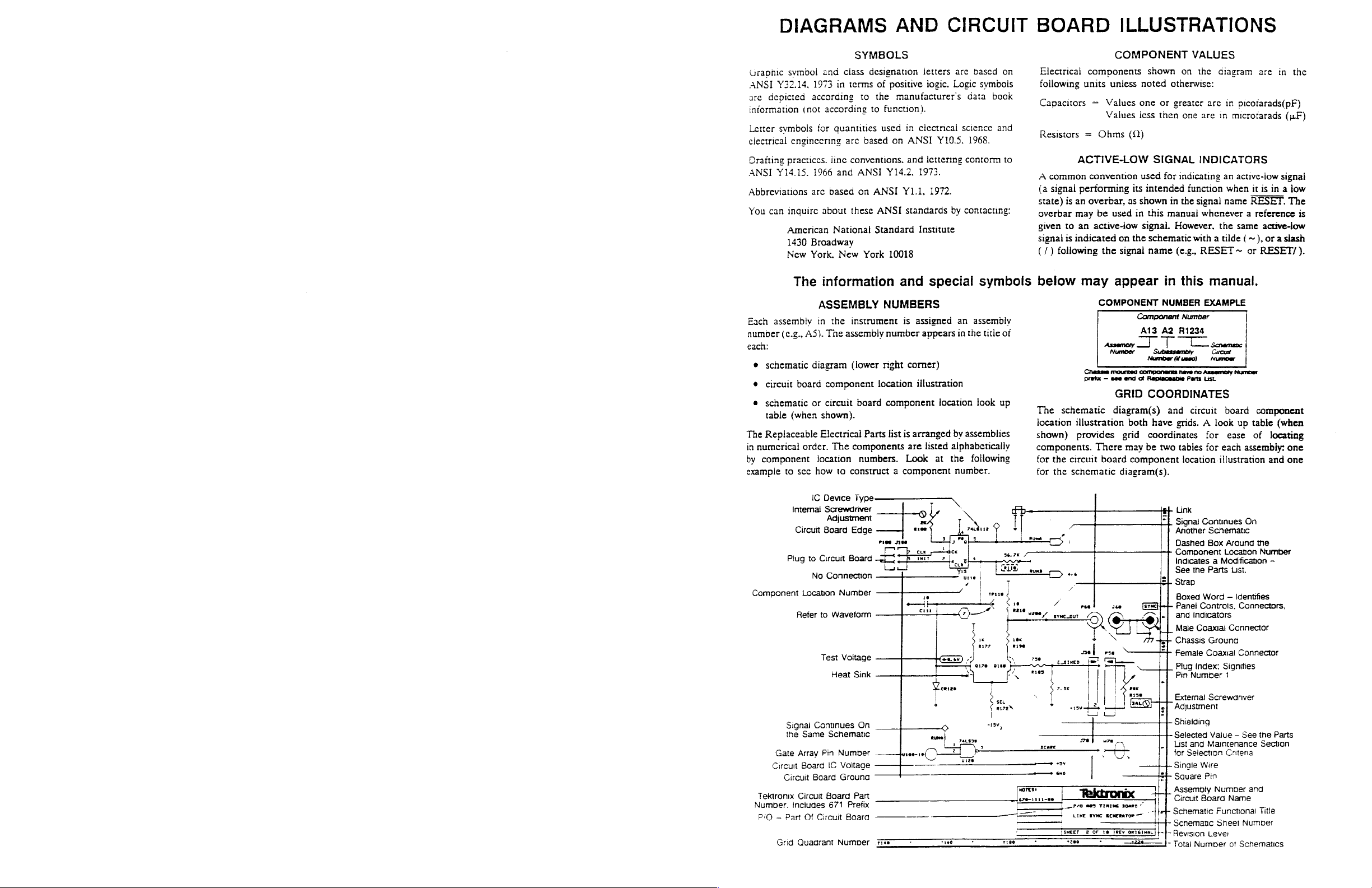
Page 82

A01 80186/80188 PGA probe adapter board component locations
Page 83

Page 84

Page 85
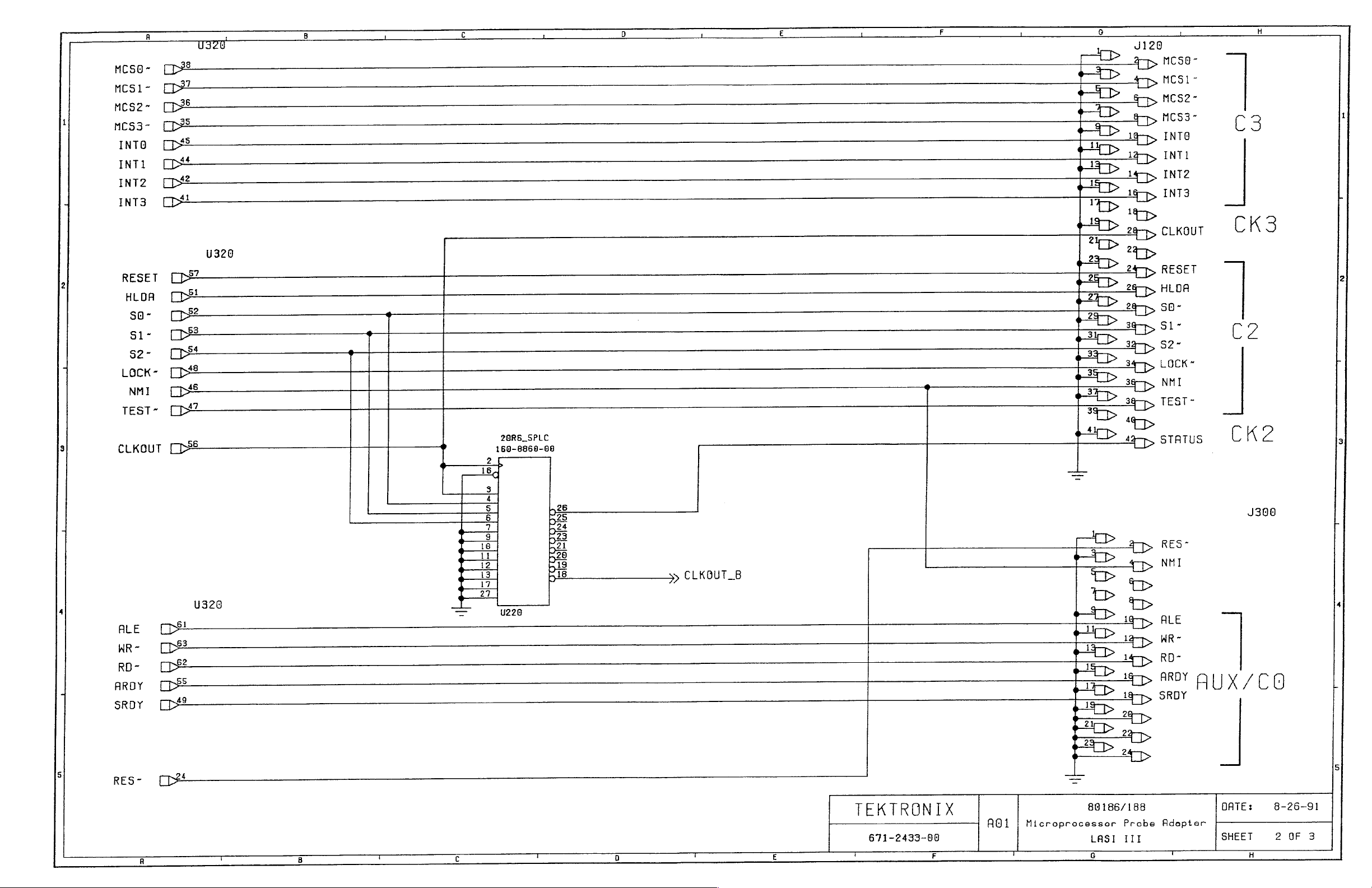
Page 86

Page 87
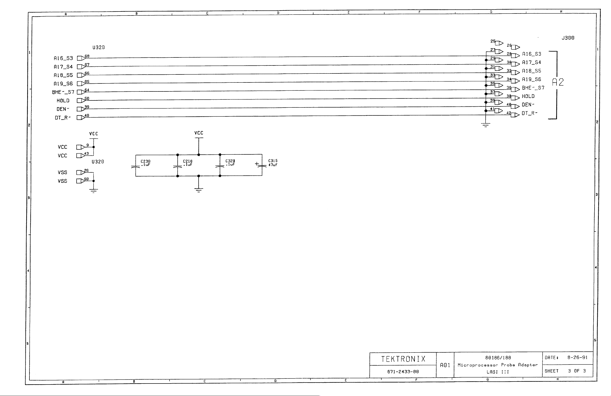
Page 88
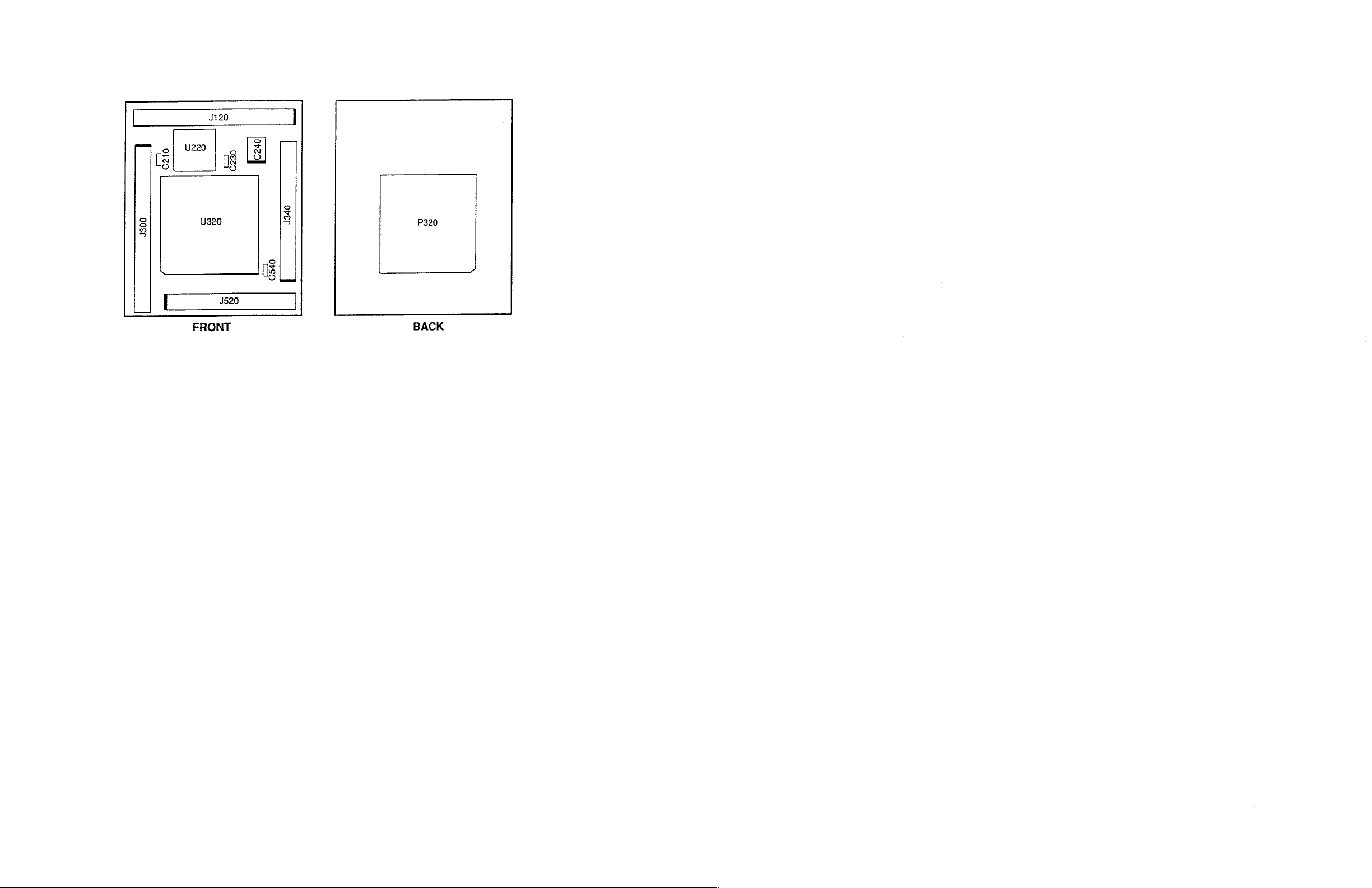
A02 80186/80188 PLCC probe adapter board component locations
Page 89
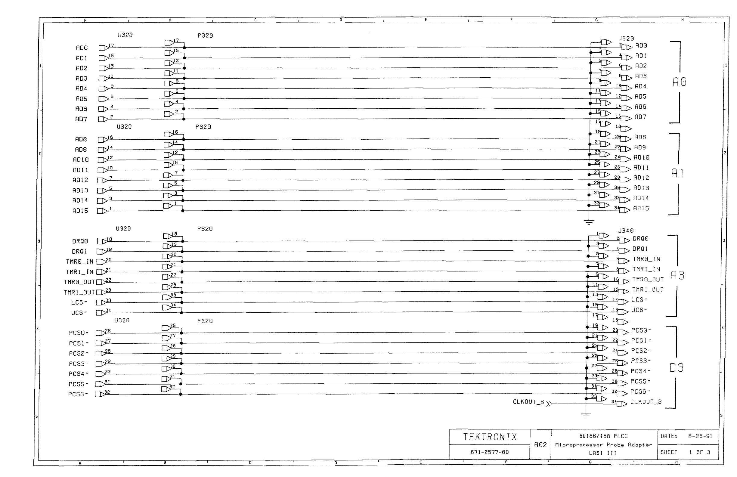
Page 90

Page 91
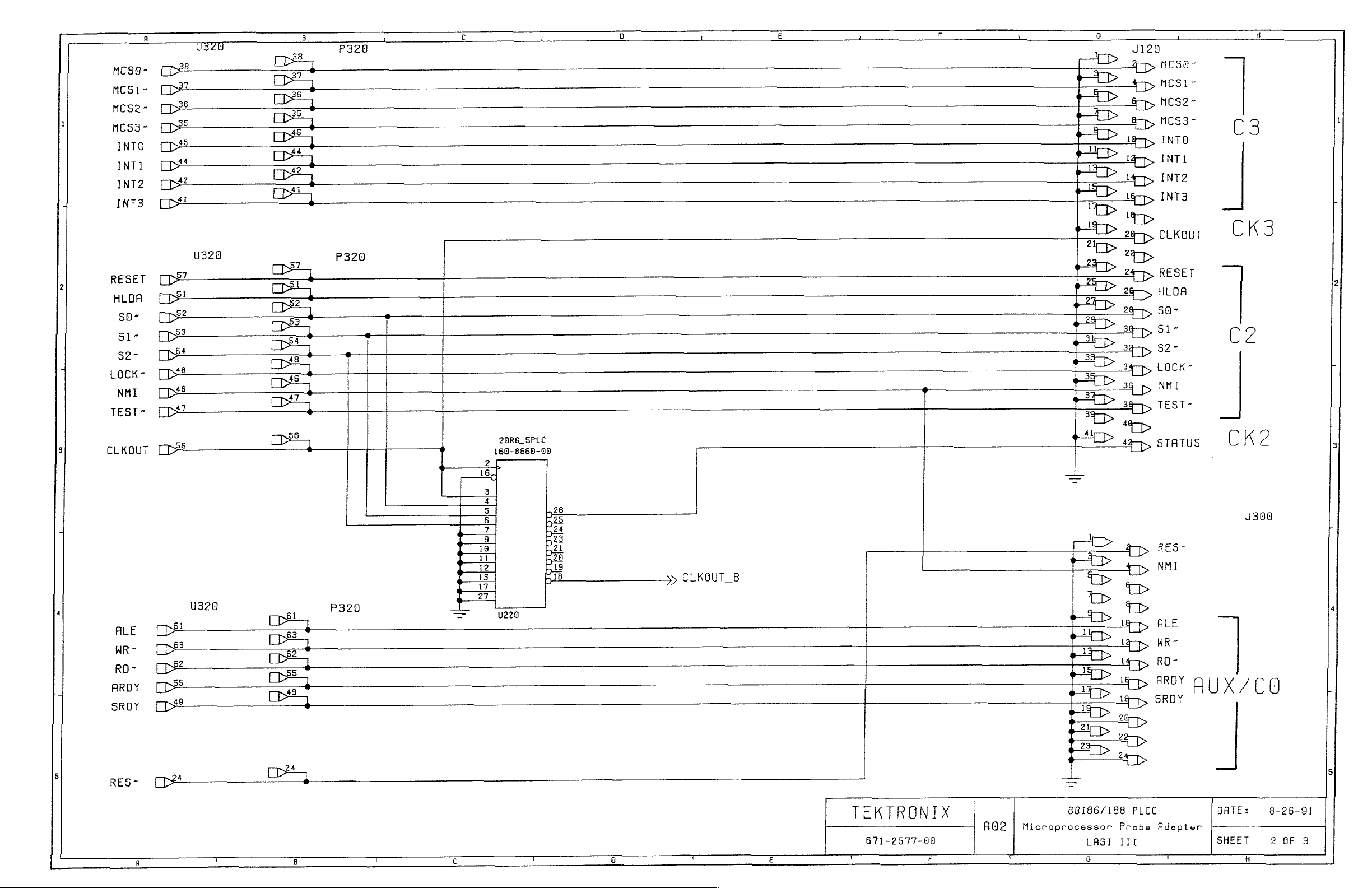
Page 92

Page 93

Page 94

 Loading...