

Page 1
070-2088-02
Tektronix, Inc.
P.O.Box 500 Beaverton, Oregon 97077 Phone 644-0767
First
Printing NOV
1975
Page 2
Page 3
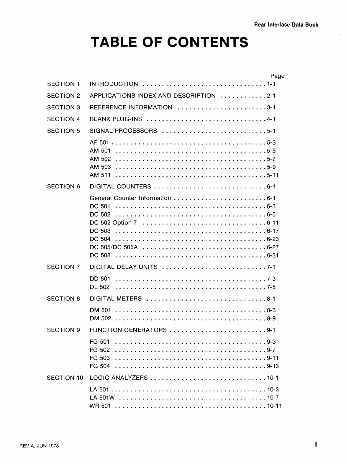
SECTION 1
TABLE OF CONTENTS
INTRODUCTION
................................
Rear Interface Data
Page
1.1
Book
SECTION 2
SECTION 3
SECTION 4
SECTION 5
SECTION 6
APPLICATIONS INDEX AND DESCRIPTION
REFERENCE INFORMATION
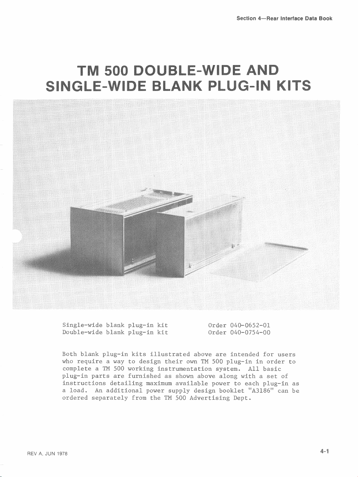
BLANK PLUG-INS
SIGNAL PROCESSORS
DIGITAL COUNTERS
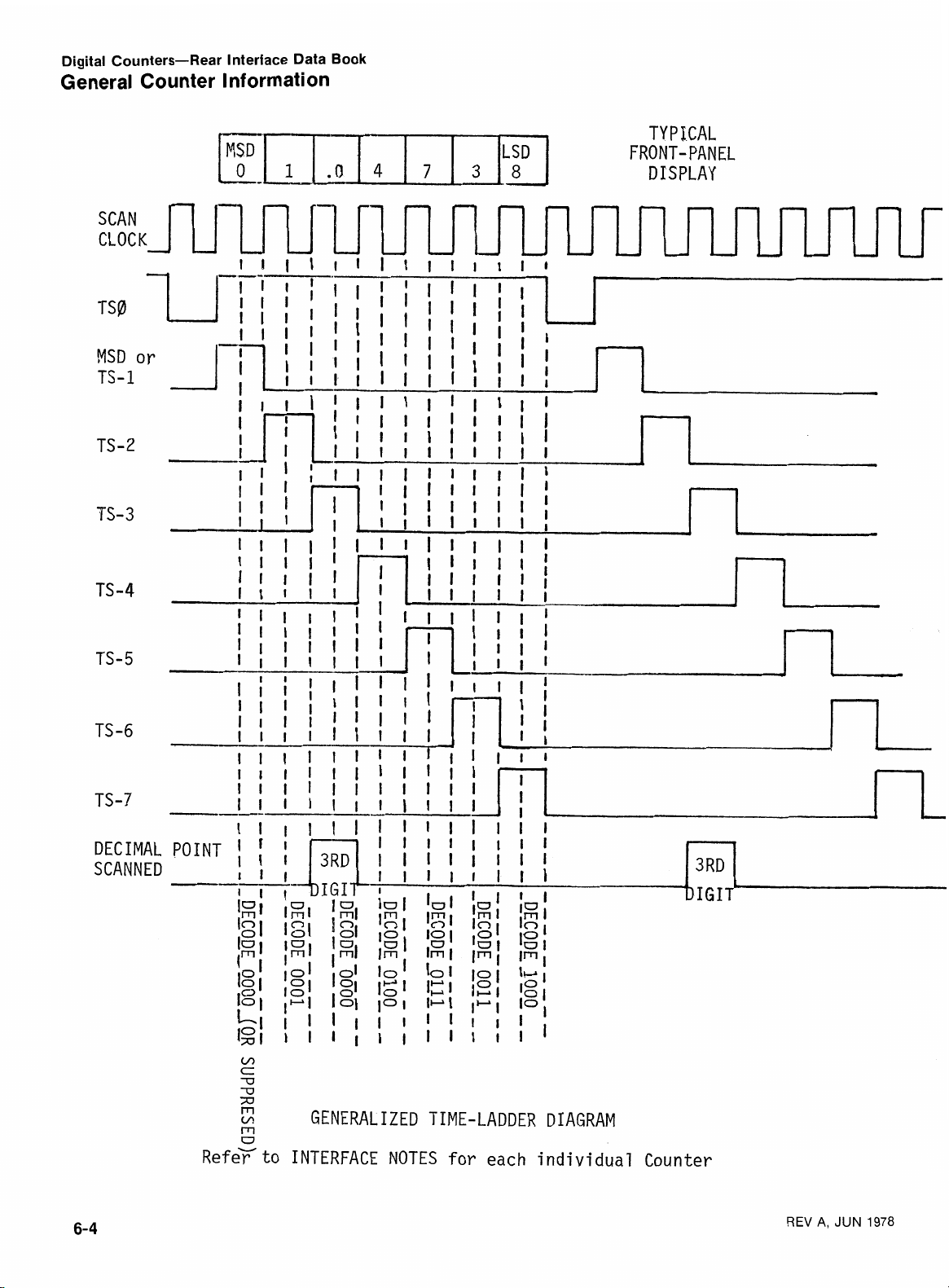
General Counter l nformation
DC501
DC502
DC 502 Option
DC503
DC504
DC 505/DC 505A
DC508
.......................................
.......................................
.......................................
.......................................
.......................................
...............................
.............................
7
................................
................................
.......................
...........................
........................
............
2.1
3.1
4.1
5.1
6.1
6.1
6-3
6-5
6.11
6-17
6-23
6.27
6-31
SECTION 7
SECTION 8
SECTION 9
SECTION 10
DIGITAL DELAY UNITS
DIGITAL METERS
FUNCTION GENERATORS 9.1
LOGIC ANALYZERS
...........................
...............................
.........................
.............................
-10-1
7.1
8.1
REV
A.
JUN
1978
Page 4
Rear Interface Data
Book
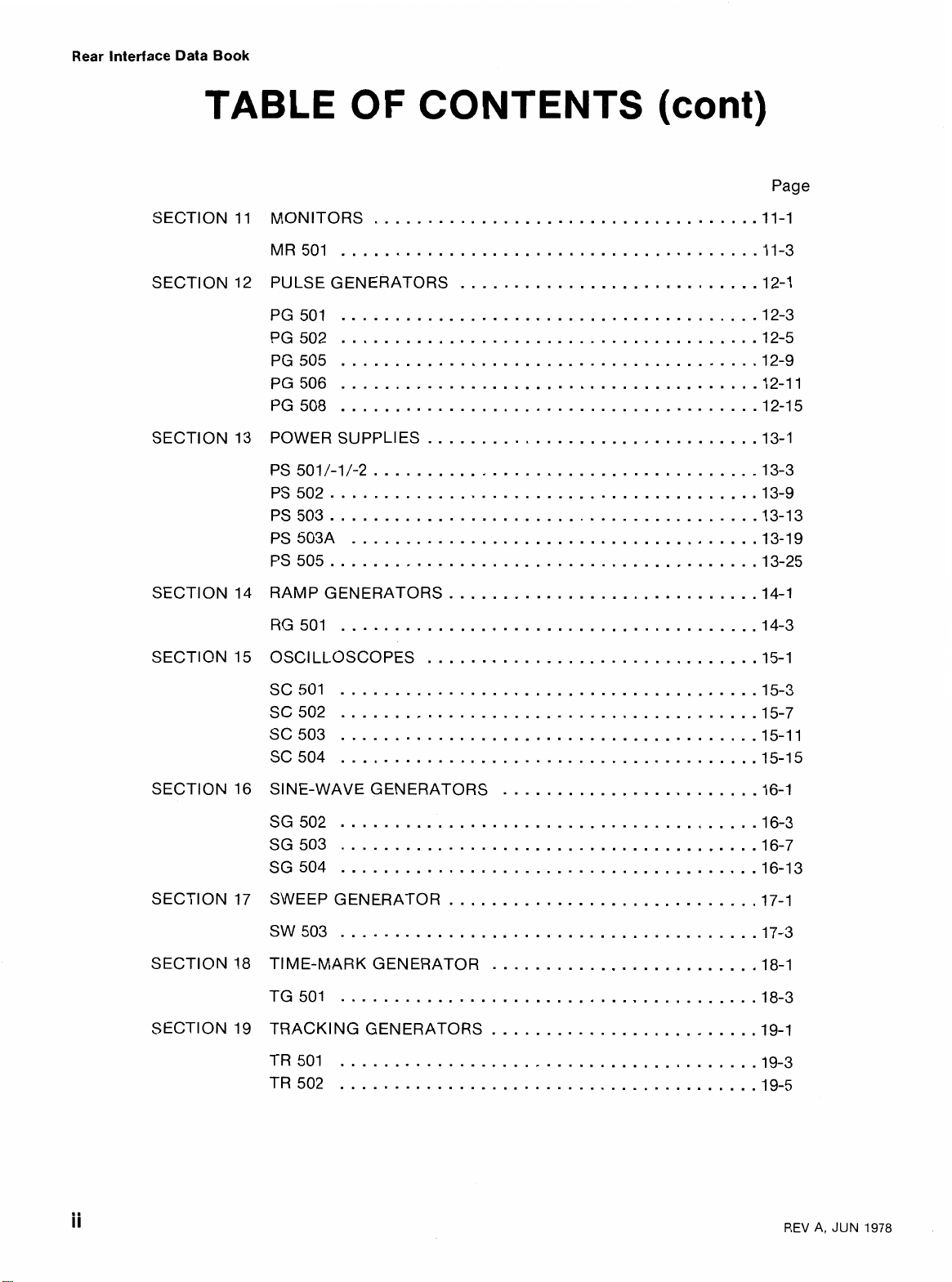
TABLE
SECTION
SECTION
SECTION
OF CONTENTS
MONITORS
11
PULSE GENERATORS
12
POWER SUPPLIES
13
(cont)
...................................
...........................
..............................
Page
.I 1.1
.I 2.1
.I 3.1
SECTION
SECTION
SECTION
SECTION
SECTION
SECTION
RAMP GENERATORS
14
15
OSCl LLOSCOPES
16
SINE-WAVE GENERATORS
17
SWEEP GENERATOR
TIME-MARK GENERATOR
18
19
TRACKING GENERATORS
............................
..............................
.......................
............................
........................
........................
-14-1
.I 5.1
-16-1
.I
7.1
.I 8.1
.I 9.1
REV
A.
JUN
1978
Page 5
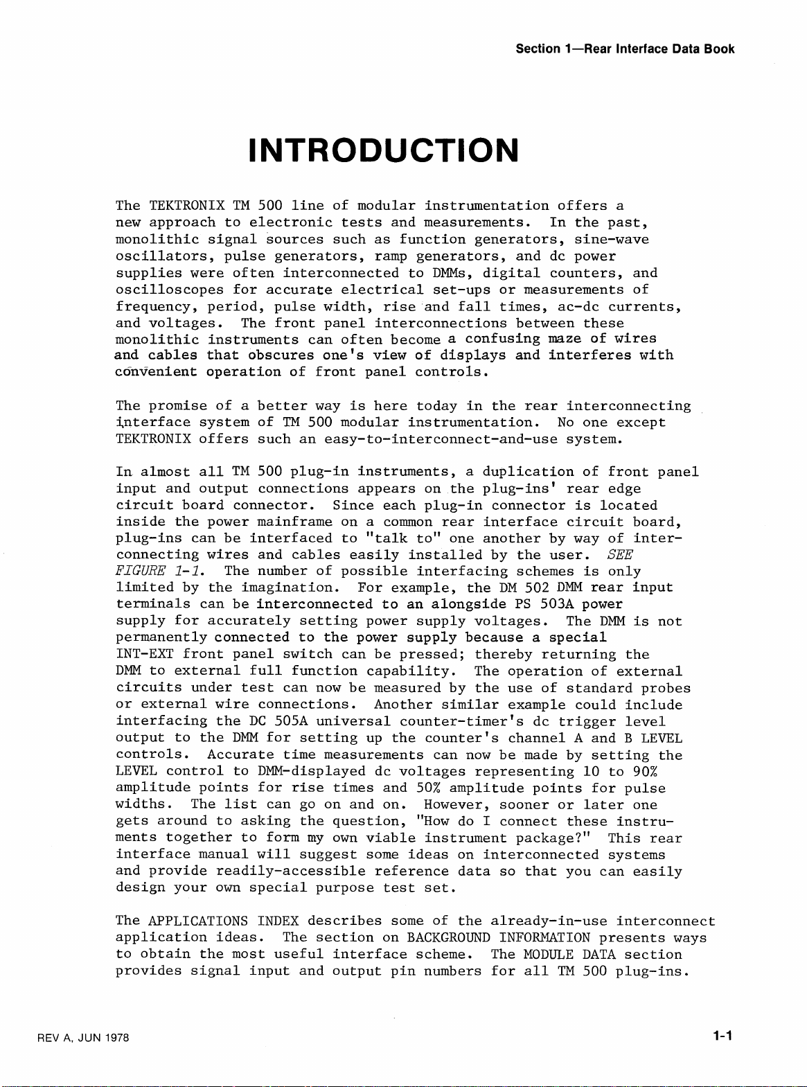
Section 1-Rear Interface Data Book
INTRODUCTION
The TEKTRONIX TM 500 line of modular instrumentation offers a
new approach to electronic tests and measurements. In the past,
monolithic signal sources such as function generators, sine-wave
oscillators, pulse generators, ramp generators, and dc power
supplies were often interconnected to
oscilloscopes for accurate electrical set-ups or measurements of
frequency, period, pulse width, rise and fall times, ac-dc currents,
and voltages. The front panel interconnections between these
monolithic instruments can often become a
and cables
that obscures one's view of displays and interferes with
convenient operation of front panel controls.
The promise of a better way is here today in the rear interconnecting
interface system of
TM
500 modular instrumentation. No one except
TEKTRONIX offers such an easy-to-interconnect-and-use system.
DMMs, digital counters, and
confusing
maze
of wires
In almost
all TM 500 plug-in instruments, a duplication of front panel
input and output connections appears on the plug-ins' rear edge
circuit board connector. Since each plug-in connector is located
inside the power mainframe on a common rear interface circuit board,
plug-ins can be interfaced to
connecting wires and cables easily installed by the user.
FIGURE
1-1. The number of possible interfacing schemes is only
limited by the imagination. For example, the DM 502
"talk to" one another by way of inter-
SEE
DMM
rear input
terminals can be interconnected to an alongside PS 503A power
supply for accurately setting power supply voltages.
permanently connected to the power
supply because a special
The DMM is not
INT-EXT front panel switch can be pressed; thereby returning the
DMM to external full function capability. The operation of external
circuits under test can now be measured by the use of standard probes
or external wire connections. Another similar example could include
interfacing the DC 505A universal counter-timer's dc trigger level
output to the
DMM
for setting up the counter's channel A and B LEVEL
controls. Accurate time measurements can now be made by setting the
LEVEL control to DMM-displayed dc voltages representing 10 to 90%
amplitude points
for rise times and 50% amplitude points for pulse
widths. The list can go on and on. However, sooner or later one
"HOW
gets around to asking the question,
ments together to form my own viable instrument package?"
do I connect these instru-
This rear
interface manual will suggest some ideas on interconnected systems
and provide readily-accessible reference data so that you can easily
design your own special purpose test set.
REV
A,
The APPLICATIONS INDEX describes some of the already-in-use interconnect
application ideas. The section on BACKGROUND INFORMATION presents ways
to obtain the most useful interface scheme. The MODULE DATA section
provides signal input and output pin numbers for all
JUN
1978
TM
500 plug-ins.
Page 6
Page 7

Introduction-Rear Interface Data Book
By the way,
presently illustrated, just drop us a pencil sketch and a
sentence describing your unique idea.
addressed as follows:
if you have a new way to interconnect
Information should be
TEKTRONIX
TM
500
P.O. Box 500
Beaverton,
,
INC
M/S
94-396
Oregon 97077
.
TM
500
not
REV
A,
JUN
1978
Page 8

Page 9
Section 2-Rear Interface Data Book
APPLICATIONS INDEX
AND
DESCRIPTION OF THE APPLICATIONS INDEX
The following APPLICATIONS INDEX was intended to be used as a
quick reference guide to a more complete description of
applications. These applications fall into two generalized categories, consisting of
multi-instrument applications. In the first case, most users are
aware of generalized instrument applications. As a result, only the
unusual single instrument applications are mentioned in the
index. Single instrument applications requiring lengthy descriptions are located under the specific instrument MODULE DATA section.
In the second case, multi-instrument applications may be either
located in the MODULE DATA section under the primary important
instrument or as an application note made available from the
TEKTRONIX TM 500 Advertising Dept. See address below.*
DESCRIPTION
(1)
single instrument applications, and
APPLICATIONS INDEX
TM
500
(2)
NOTE:
*
See fo
DC 505A Trigger Level Output
Network Attenuation or Gain Measurement
PS 503A Voltage Regulation via Remote Sensing
PS 503A Output Voltage Controlled by External Resistance
Programming
PS 503A Output Voltage Controlled by External Voltage
Programming
Waveform Generation System
Integration through V to
Function Generator Swept Frequency Applications
Power Supplies Driven by Signal Sources
AC Microvoltmeter
TEKTRONIX,
P.
0. Box 500
l
lowing pages for app Zication descriptions.
INC.
Advertising Dept., M/S
Beaverton, Oregon 9 70
76-260
7
7
F
Conversion
REV
A.
JUN
1978
Page 10
Applications Index and Description-Rear Interface Data Book
1.
DC 505A TRIGGER LEVEL OUTPUT CONNECTION
TO AN ALONGSIDE DMM
Any
TM
500
DMM
can be used to read out the A and B trigger "level
DC
outff of the
facing feature
A
interval
-+
505A
is
B
measurements.
universal counter. The benefit of this inter-
improved accuracy in making width B and time
These features are acquired by using a
the
DC
505A
gate lamp,
to measure the
DMM,
+E
in conjunction with
peak and the
-E
peak levels
of the pulse train to be counted. The peak-to-peak measurement
then used to determine the correct setting of the level controls
for the measurement of interest.
The actual connections between the
DMM
and
DC
505A
are made as
illustrated below:
DMM
28B
28A
2.
NETWORK ATTENUATION OR GAIN MEASUREMENT
+
+
signal
ground
The dBm or dBV measurement capability of the
DC
505A
-+
22A
-+
17A
'
DM
502
can be used
to measure the attenuation or gain of a network under test when
driven by an SG
502
audio generator. Audio network analysis can be
performed on networks such as filters and amplifiers.
is
Upon completion of interface connections (see below), operation
consists of pressing
Press back to
loss in dB
EXT
is
obtained by subtracting the input and output levels.
DM
502
INT
button to read network input level.
for network output level. The network gain or
The actual connections between instruments to be interfaced follow:
3.
The
plus or minus
502
SG
28A
(SIG OUT)
27A
(SIG GND)
FRONT PANEL
BNC
OUT
-
-
PS
503A VOLTAGE REGULATION VIA REMOTE SENSING
20
V
NETWORK
-
-
INPUT (SIG)
INPUT
OUTPUT
OUTPUT
(GND)
(SIG)
(GND)
DM
502
28B (HI)
28A
(LO)
-
-
FRONT PANEL
FRONT PANEL (LO)
(HI)
power supply regulation can be improved by
REV
A,
JUN
1978
Page 11
Applications Index and Description-Rear Interface Data
Book
remote sensing
DATA section.
4.
at
the load. For more details see PS 503A MODULE
PS 503A OUTPUT VOLTAGE CONTROLLED
BY
EXTERNAL
RESISTANCE PROGRAMMING
The plus or minus 20 V power supply can be controlled via resistance
programming through the
program resistance values and interconnections may be found in the
PS 503A MODULE DATA section.
5. PS 503A OUTPUT VOLTAGE CONTROLLED
rear
interface. Specific details on
BY
EXTERNAL
VOLTAGE PROGRAMMING
The plus or minus 20 V power supplies can be controlled via an
external voltage source through the rear interface.
supplies can now be independently swept from
slew
interconnection and external voltage control information may be
found in the PS 503A MODULE DATA section.
rate depends on the load and the output voltage d~/dt. Specific
6.
GENERATING COMPLEX WAVEFORMS WITH TM 500 INSTRUMENTS
0 to 20 volts. The
One or both
The generation of a variety of differently-shaped signals can be
produced by an RG 501 Ramp Generator, two PG 505 Pulse Generators,
and an
such
provide a means of determing signal periods, durations,
fall
For complete details on this Waveform Generation System, write the
TM 500 Advertising Dept. for application note #75M 1.0.
Measurement transducers are often used to produce a voltage that
is
liquid, or electrical energy. But, frequently
to know the total number of units that have been measured by the
transducer during some
it
particular TM 500 instruments can be configured together to provide
this voltage to frequency conversion. The transducer output
first processed by a signal conditioning
Amplifier. The resulting output
frequency conversion in a function generator such as an FG 501 or
FG 502. The output frequency
counter. For more complete information on this application, write
the TM 500 Advertising Dept. for application note #75M 2.0.
AM
501 Operational Amplifier.
as
the SC 501 or SC 502 can be used along with this system to
times,
proportional to the
is
to know the
delay
7.
times
INTEGRATION THROUGH V TO F CONVERSION
rate
as
well as peak-to-peak signal amplitudes.
rate
time
at any particular point in
of flow of something like a gas, a
interval like a second or a day, than
is
An alongside TM 500 oscilloscope
rise
and
it
is
more important
time.
AM
501 or
is
applied to produce an analog to
displayed on an alongside digital
AM
Three
is
502 Operational
REV
A,
JUN
1978
Page 12
Applications Index and Description-Rear Interface Data Book
8.
FUNCTION GENERATOR SWEPT FREQUENCY
AND TWO-TONE APPLICATIONS
Although this application was written specifically for the FG 501,
the underlying principles apply equally
function generators such as the FG 502 and FG 503.
generator can be made to change
by the instantaneous applied voltage appearing at the VCF input
connector. For example, a voltage ramp applied to the VCF input
will
be used for FSK applications where the FG 501 dial setting
mark frequency and the positive amplitude
For more complete information on this application, write the TM 500
Advertising Dept. for the application note entitled "FG 501 Swept
Frequency
provide a linear change in output frequency.
tage will provide two output tones, the output frequency of which
determined by the specific levels of the top and bottom portions of
the square wave. For example, the two-tone output capability could
application^.^'
its
well
output frequency as determined
to the more recent
A
function
A
square-wave vol-
is
the space frequency.
is
BNC
the
is
9.
POWER SUPPLIES DRIVEN
Any of the analog programmable power supplies such as PS 501,
PS 503, or PS 503A plug-ins can be driven by an adjacent signal
or function generator to provide a low source impedance suitable
for delivering higher currents into
load examples would include drive relays, lamps, small motors,
loudspeakers,
output frequency and
Specific information on voltage driving power supply sense inputs
can be found in the MODULE DATA section under Power Supply
Notes.
The
AM
502 and
When the
interface SIGNAL
to the
DM
the
display on the 2-volt ranges. This measurement application can be
used in setting up low audio signal output levels from an adjacent
audio signal source such as the SG 502.
AM
DM
501
etc.
DM
501
501's rear
will
The power supply
risetime
10.
501 can provide ac and dc microvolt measurements.
is
set
for a gain of 1000 (dc-coupled) and
OUT
(28A) and SIGNAL OUT GROUND (27A) are connected
HI
INPUT (28B) and LO INPUT (28A), respectively,
provide a 2 millivolt dc or ac full scale digital
up to
MICROVOLTMETER
BY
SIGNAL SOURCES
a
low impedance load. Some
will
its
follow the signal sources
slew rate limitations.
Interface
its
rear
REV
A,
JUN
1978
Page 13
Section 3-Rear Interface Data Book
REFERENCE INFORMATION
This section contains the following topics: Interface Circuit Boards,
Interface Compatibility, Family Barrier Keys, Interfacing the Standard
Mainframe, Interfacing the Option 2 Mainframe, Quick Change Interfacing,
7
External Interfacing, Option
and a Table of Plug-in and Mainframe Power Requirements.
Mainframes, Product Modification
INTERFACE CONNECTIONS
Kits,
The plug-in rear interconnections are made
mainframes module interface circuit board.*
this board are mounted double edge
plug-in modules.
--
OF BOARD
COPJNECTORS
Each 28-pin connector
mainframe bottom and ending with number 28 near the top. However,
only pin numbers starting with 14 through 28 are used for signal line
data interfacing.
mainframe power to the instruments. In the section on module data,
a rear view of only signal line contacts
user applications. Since each plug-in connector has a double row of
contacts, the left column (as viewed from the rear of the mainframe
or instrument)
actual interface connection techniques are described in the remaining
portions of this section.
-.
is
/REAR
is
Pins
designated as B and the right column as
1
OF
numbered starting with number
through 13 are used for connections from
28 pin connectors for accepting
at
the rear of the power
See Figwe
14 through 28
3-1. On
TM
504
REAR
INTERFACE
CIRCUIT BOARD
1
near the
is
given for
A.
The
REV
A,
JUN
*NOTE:
1978
The
TM
525
rear interconnections are made at the front of the
interface circuit board.
Page 14
Reference Information-Rear Interface' Data Book
INTERFACE COMPATIBILITY
An
important feature of the
instruments in a mainframe to each other, or to external equipment, via
the "rear interface". Physically, the rear interface consists of
upper 30 edge-card connections at each plug-in compartment, (2) optional
connectors on the mainframe rear panel, and
to make connections from plug-in to plug-in, or from plug-in to rear connector, and hence to external equipment.
TM
500-Series
is
the ability to interconnect
(3)
any wiring or cabling used
(1)
the
The wiring or cabling portion of most
tomer installed.
A
large number of unique interconnections are possible.
Because of the variety of instruments
TM
500 interconnect systems
comprising the
TM
500 family,
is
cus-
it
was
decided to make the interface a custom system with no factory installed bus
lines or truly "standard" pin assignments. However, instruments are grouped
I/O
into families with similar
which permits physical lockout of plug-ins from other families.
characteristics and an optional keying system
Use of the
optional keying system (with barrier keys) minimizes the possibility of introducing the wrong plug-in into a mainframe compartment when the mainframe
has been wired for specialized rear interface connections. However, the
assignment of family keys
not intended to make sure that a system
will
be
is
fully functional when plug-ins are installed, only that nothing destructive
of hardware (internal or external)
will
stalled. In other words, the main compatibility rules
occur if the wrong plug-in
are:
is
in-
Instruments having dissimilar input/output characteristics are grouped
into different families.
system,
it
is
possible that installing a plug-in of the wrong family
may be destructive of hardware.
If the rear interface
Install family barrier keys in the
is
wired to configure a
mainframe to avoid possible damage to equipment.
Although family members have similar input/output characteristics,
their basic functions may differ drastically.
Only a keying system
with a unique key or combination for every individual instrument type
would assure system operation.
Therefore,
it
is
only required that
family members are neither conducive nor susceptible to hardware failure (destructive)
if plugged into a compartment wired for a different
member of the same family.
FAMILY BARRIER KEYS
A
barrier key
contact pins located in the power module circuit board edge connector.
See Fig.
ules that are electrically incompatible.
result of inserting plug-in modules into a mainframe that has been prewired
for a different
classified into family categories.
ments are listed in the following table.
20 barrier keys, order Tektronix Part Number 214-1593-02 from your local
TEKTRONIX
is
a special plastic part designed to be inserted between
3-1.
Its
function
set
Field Office.
of
is
to prevent possible damage to plug-in mod-
TM
500 instruments.
Incompatability can arise as the
Compatible plug-in modules are
The categories and barrier key assign-
If you require an extra set of
REV
A,
JUN
1978
Page 15
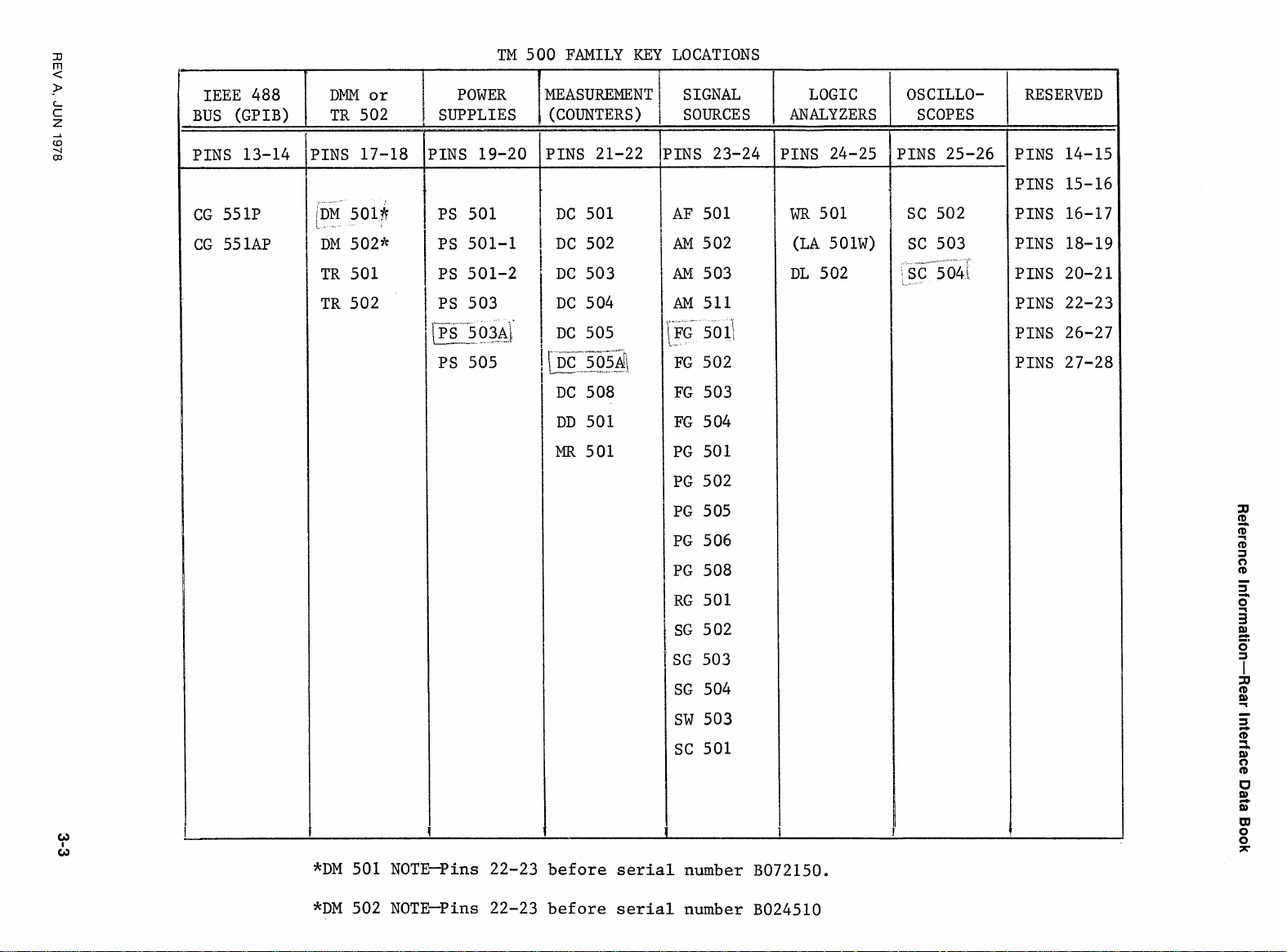
TM 500 FAMILY KEY LOCATIONS
IEEE
BUS
PINS 13-14
488
(GPIB)
DMM
or
TR 502
'INS 17-18
POWER
SUPPLIES
INS 19-20 IPINS 21-22
MEASUREMENT
(COUNTERS
)
INS 23-24
SIGNAL
SOURCES
LOGIC
ANALYZERS
WR
501
(LA 501W)
OSCILLO-
SCOPES
RESERVED
PINS 14-15
PINS 15-16
PINS 16-17
PINS 18-19
PINS 20-21
PINS 22-23
PINS 26-27
PINS 27-28
*DM 501 NOTE-Pins 22-23 before
*DM 502 NOTE-Pins 22-23 before
serial
serial
number B072150.
number B024510
Page 16
Reference Information-Rear Interface Data Book
With a barrier in place in the mainframe connector,
instruments belonging to one of the above-listed families cannot
be inserted into the mainframe wired for a different plug-in
is
family. The key to this lockout feature
of the barrier key into the double edge 28-pin connector.
plug-ins belonging to a specific family can be inserted into the
module compartment containing the desired family key because of
a corresponding slot cut into the mating plug-in circuit board
at the family key location.
INTERFACING TM 500
the actual placement
plug-in
All
THE STANDARD MAINFRAME
The standard mainframe purchased without any options comes without
square pin connectors.
can be accomplished by hand soldering interconnecting wires or
coaxial cables between pin locations at the rear* of the mainframe
rear interface circuit board.
insulated wire varying in sizes according to current-carrying
capabilities can be used for low frequency or dc circuits. Miniature
50Q coaxial cables should be used in high frequency signal environments
to eliminate potential crosstalk problems.
Any interfacing between plug-in compartments
See Figure
3-2.
A
good quality
SPECIAL NOTES ON ORDERING COAXIAL CABLES
NOTE #l.
NOTE #2.
Small 50R coaxial cable by the foot.
If
you require a quantity of small diameter 50R
coaxial cab le, order TEKTRONIX part nwnber 1 75- 1020-00
by the foot.
Small 50R coaxial cable with pre-installed special
PeZtoZa connectors on each end.
Some plug-in
instruments do not have all inputs or
outputs factory-wired to the rear and thus require
special internal connections prior to rear interface
use. In special cases of this nature, the required
information can be fomd under the MODULE DATA section
pertaining to the plug-in of interest.
small diameter 50R coakal cable with special PeZtoZa
connectors on each end, then measure and order the
optimwn length from the following list
If you require
of
cables.
*NOTE:
Front
in
the
TM
-
-
515
T~aveler mainfmme.
REV
A,
JUN
1978
Page 17
Page 18
Reference Information-Rear Interface Data Book
IWORTANT NOTE:
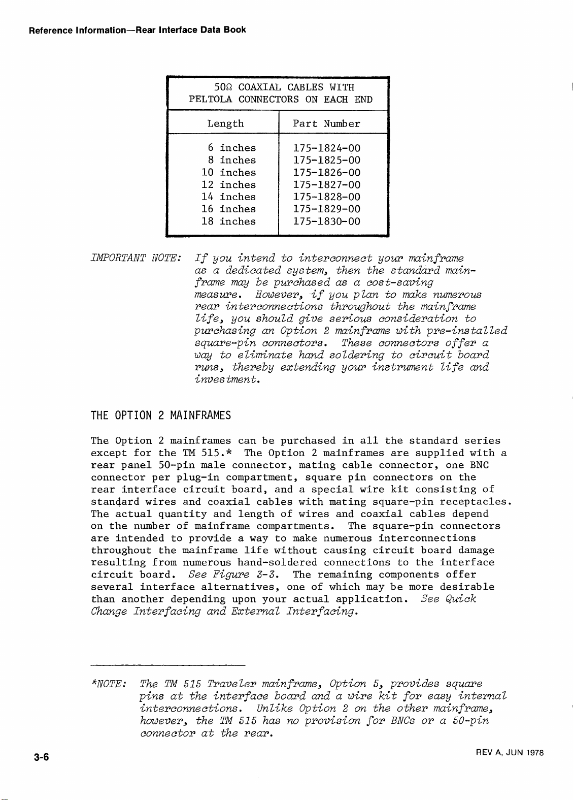
50f2 COAXIAL CABLES
PELTOLA CONNECTORS
Length
6
inches
8 inches
10 inches
12 inches
14
inches
16 inches
18 inches
Part Number
ON
WITH
EACH
END
If you intend to interconnect your mainframe
as a dedicated system, then the standard mainframe may be purchased as a cost-saving
measme. However, if you plan to make numerous
rear interconnections throughout the mainframe
life, you should give serious consideration to
2
purchasing an Option
mainframe with pre-installed
square-pin connectors. These connectors offer a
way to eliminate hand soldering to circuit board
runs, thereby extending your instrument life and
investment.
THE OPTION 2 MAINFRAMES
The Option 2 mainframes can be purchased in all the standard series
except for the
rear panel 50-pin male connector, mating cable connector, one
connector per plug-in compartment, square pin connectors on the
rear interface circuit board, and a special wire kit consisting of
standard wires and coaxial cables with mating square-pin receptacles.
The actual quantity and length of wires and coaxial cables depend
on the number of mainframe compartments. The square-pin connectors
are intended to provide a way to make numerous interconnections
throughout the mainframe life without causing circuit board damage
resulting from numerous hand-soldered connections to the interface
circuit board.
several interface alternatives, one of which may be more desirable
than another depending upon your actual application.
Change Interfacing and External
"NOTE: The
pins at the interface board and a wire kit for easy internal
interconnections.
however, the
connector at the rear.
TM
515.h The Option 2 mainframes are supplied with a
See Figure
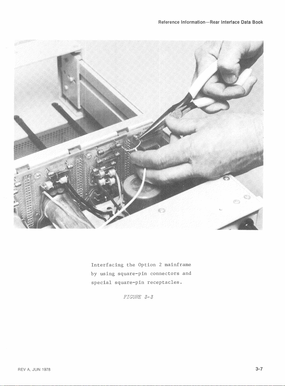
3-3.
The remaining components offer
Interfacing.
TM
515 Traveler mainframe, Option
Unlike Option
TM
515
has
no
provision for BNCs or a 50-pin
See Quick
5,
provides square
2
on the other mainframe,
BNC
REV
A,
JUN
1978
Page 19
Page 20
Reference Information-Rear Interface Data Book
QUICK CHANGE INTERFACING
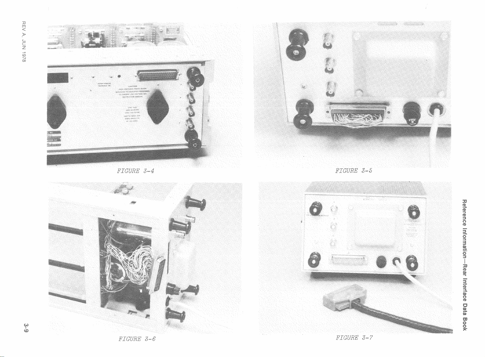
The quick change interfacing feature makes use of a special set
of male-female multi-pin connectors located at the rear of the
mainframe.
See Figure
3-4. The female multi-pin connector may
be thought of as a programmer connector.
change interfacing technique can prewire as many programmer
connectors as required for each individual instrumentation set-up.
After inserting the desired plug-ins into preselected mainframe
compartments, the prewired programmer connector is inserted into
the counterpart male muli-pin connector on the rear of the mainframe.
See Figure
3-5. The prewired interconnections on the programmer
connector now interconnect the desired plug-ins so that they can
"talk" to one another.
The quick change interfacing technique
allows the user to quickly change instrumentation set-ups by
(1)
selecting the new plug-in configuration, and (2) choosing the
correct prewired programmer connector for that specific instrumentation set-up
.
The user of the quick
The photograph of Figure
3-6
illustrates how the Option 2 mainframe
can be wired to permit use of the quick change interfacing technique.
These connectors are not factory-wired in order to give a system
designer as much flexibility as possible. Instead, prepared
jumper wires, coaxial cables, a rear 50-pin connector, and associated
hardware are included along with each Option 2 mainframe.
Hence,
there are no pin assignments for rear panel connectors because of
the wide variety of possible connections.
The external programmer connectors for quick change programming
can be ordered from the list of hardware materials below.
--
50-PIN
FEMALE
PROGRAMMER
HARDWARE
Part Number Description Quantity
1
131-1319-00 Cover, conn; molded plastic
each
wlhardware
131-1345-00 Conn, rcpt, elec: 50 contact female
1
each
EXTERNAL INTERFACING
The external interfacing technique makes use of the Option
2-
supplied 50-pin rear male connector as a means to interface with
equipment external to the
TM
500 system.
See Figure
3-7.
Users
can order additional hardware to make up a completed plug-on external
connector from the Following parts list.
REV
A,
JUN
1978
Page 21
Page 22
Reference Information-Rear Interface Data Book
Part Number
131-1319-00
131-1345-00
WTE:
The number of wires contained within the external connector
cable depends upon the specific user's requirements.
EXTERNAL
Cover, conn; molded plastic wlhardware
Conn, rcpt, elec: 50 contact female
CABLE CONNECTOR
50-PIN FEMALE
Description
HARDWARE
CONNECTOR
Quantity
1
each
1
each
The
external multi-conductor cable should be obtained from a
ZocaZ multi-conductor cab Ze supplier or vendor.
CAUTION:
Center for service, please notify the service center that the mainframe has been 'interfaced.
return of your instrument.
module and plug-in(s) to the service center.
In the event your mainframe
This
It
will
is
advisable to return both power
is
sent to a TEKTRONIX Service
save money and expedite the
THE OPTION 7 MAINFRAMES
The following described bus wires and barrier keys are added to the
'EM
rear interface connector boards in the following
modules in order to provide rear interface connections between the
DC
508 Option 7 Counter (or other Option 7 counters), TR 502 Tracking
Generator, and SW 503 Sweep Generator.
Bus Wires. Six-conductor ribbon cable (Tektronix Part Number
00)
TM
is
used to make bus runs between the
503,
TM
504,
TM
506, TM 515
following points.
B14 on J10, 520, and 530
B15 on J10, 520, and 530 J10, 520, and 530
B16 on J10, 520, and 530 are plug-in connectors.
B17 on
J10, 520, and 530 See Power Module instruction
I318 on J10, 520, and 530 Manual.
A18 on J10, 520, and 530
Plastic barrier keys (Tektronix Part Number 214-1593-02) are inserted
between pins 21 and 22 on J10 (Counter slot), between pins 23 and 24
on 520 (Sweep Generator slot), and pins 17 and 18 on 530 (Tracking Generator slot).
500-series power
175-0829-
Once the above bus connections are made and barrier keys inserted, the
three connectors so changed are system dedicated and the three slots
should be used only for system-dedicated
plug-En modules.
REV
A,
JUN
1978
Page 23
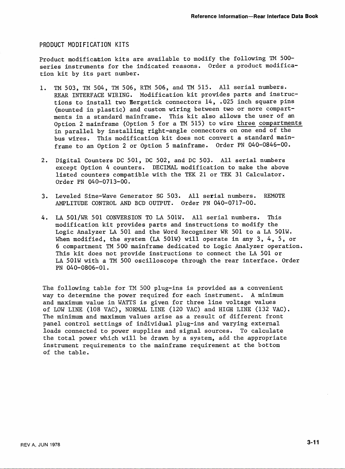
PRODUCT MOD1 FICATION KITS
Reference Information-Rear Interface Data Book
Product rnodificta.&ion kits are available to modify the following
series
tion kit by
instruments for the indicated reasons. Order a product modifica-
its
part number.
All
TM
503,
REAR
TM
504, TM 506,
INTERFACE
WIRING.
RTM
506, and
TM
Modification kit provides parts and instruc-
tions to install two Bergstick connectors
(mounted in plastic)
and custom wiring between two or more compart-
515.
14, -025 inch square pins
serial numbers.
ments in a standard mainframe. This kit also allows the user of an
TM
Option 2 mainframe (Option 5 for a
515) to wire three compartments
in parallel by installing right-angle connectors on one end of the
bus
wires.
frame to an Option
Digital Counters
except Option 4 counters.
This modification kit does not convert a standard main-
2
or Option 5 mainframe. Order PN 040-0846-00.
DC
501,
DC
502, and
DC
503.
All
serial numbers
DECIMAT., modification to make the above
listed counters compatible with the TEK 21 or TEK 31 Calculator.
Order PN 040-0713-00.
All
Leveled Sine-Wave Generator SG 503.
AND
BCD
AMPLITUDE CONTROL
OUTPUT. Order PN 040-0717-00.
LA 5011~~ 501 CONVERSION TO LA 501W.
serial numbers. REMOTE
All
serial numbers. This
modification kit provides parts and instructions to modify the
Logic Analyzer LA 501 and the Word Recognizer
When modified, the system
6 compartment
TM
500 mainframe dedicated to Logic Analyzer operation.
This kit does not provide instructions
TM
LA 501W with a
500 oscilloscope through the rear interface. Order
(LA
501~)
will
to connect the LA 501 or
WR
501 to a LA 501W.
operate in any 3, 4, 5, or
PN 040-0806-01.
TM
500-
REV
The
following table for
way to determine the power required for each instrument.
and maximum value in WATTS
of LOW LINE (108 VAC), NORMAL LINE (120 VAC) and
TM
500 plug-ins
is
given for three line voltage values
is
provided as a convenient
A
HIGH
LINE (132 VAC).
The minimum and maximum values arise as a result of different front
panel control settings of individual plug-ins and varying external
loads connected to power supplies and signal sources. To calculate
the
total power which
will
be drawn by a system, add the appropriate
instrument requirements to the mainframe requirement at the bottom
of the table.
A,
JUN
1978
minimum
Page 24
Reference Information-Rear Interface Data Book
POWER REQUIREMENTS FOR
Low Line - 108
VAC
Instrument Min.Watts Max. Watts
'I'M
500
PLUG-INS
Nominal Line - 120
Min.
Watts Max. Watts Min. Watts Max. Watts
AND
MAINFRAMES
VAC
High Line
-
132
VAC
TM
TM
TM
TM
RTM
TM
501
503
504
506
506
515
REV A,
JUN
1978
Page 25
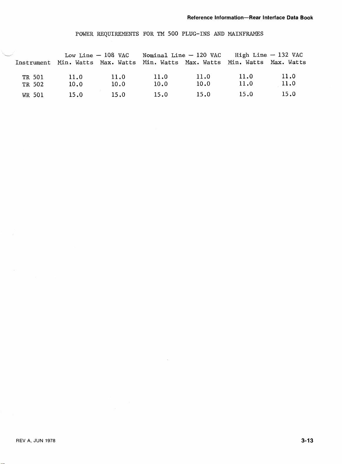
Reference Information-Rear Interface Data Book
POWER WQUIIXEXENTS
L-
Low Line - 108
VAC
FOR
TM
500 PLUG-INS
Nominal Line - 120
AND
VAC
MAINFRAJ!ES
High Line - 132
Instrument Min. Watts Max. Watts Min. Watts Max. Watts Min. Watts Max. Watts
VAC
REV
A,
JUN
1978
Page 26
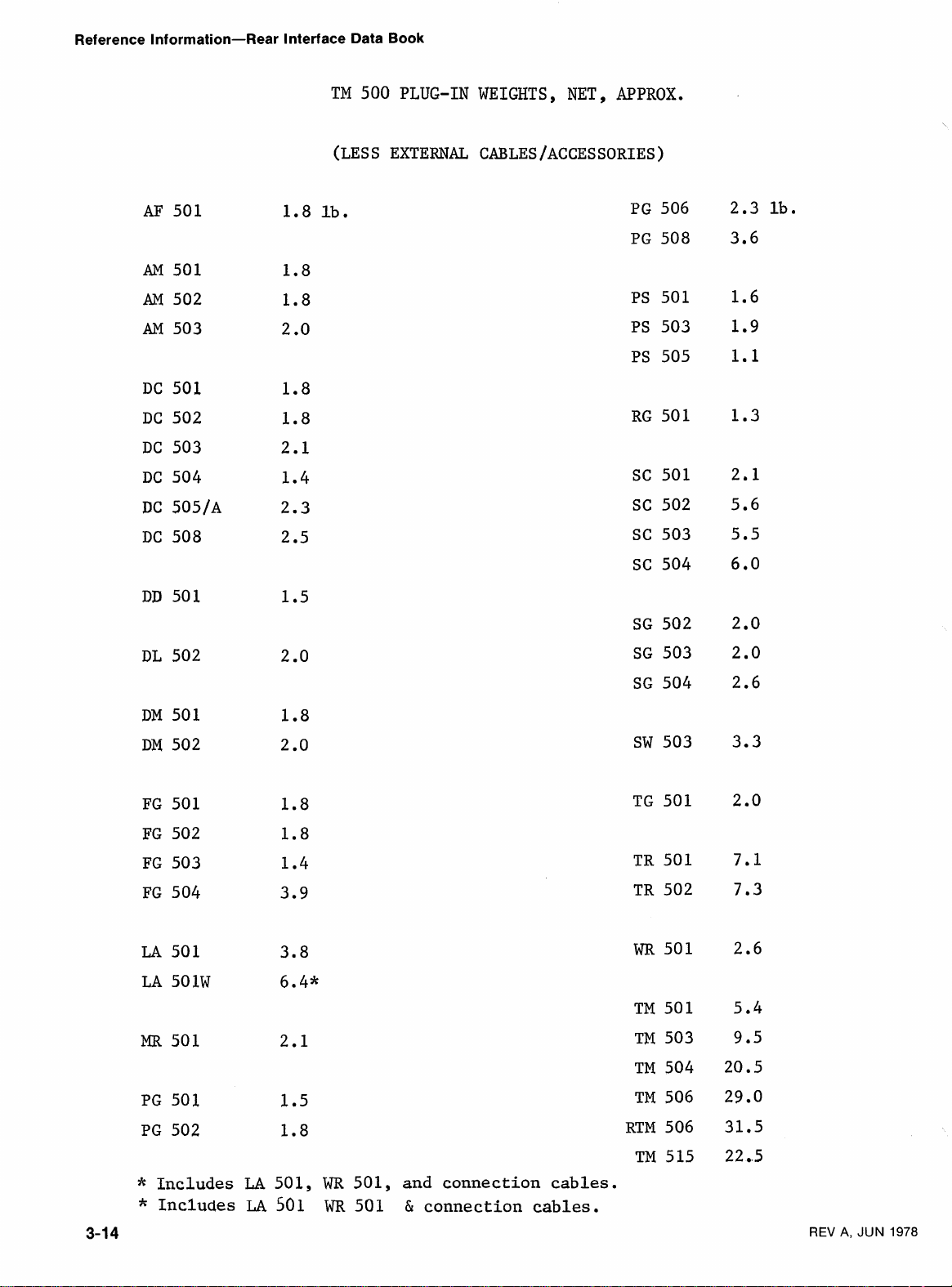
Reference Information-Rear Interface Data Book
TM
500
PLUG-IN WEIGHTS, NET, APPROX.
(LESS EXTERNAL CABLES/ACCESSORIES)
1.8 lb.
1.8
1.8
.o
2
1.8
1.8
2.1
la4
2.3
2.5
1.5
2 a0
2.3 lb.
3.6
1.6
1.9
1.1
1.3
2.1
5.6
5.5
6.0
2.0
2.0
2.6
3-1
*
*
4
Includes
Inclucies
LA
LA
1.8
2.0
501,
501
WR
501, and connection cables.
WR
501
&
connection
cables.
WR
501
TM 501
TM 503
TM 504
TM 506
RTM 506
TM 515
3.3
2.0
7.1
7.3
2.6
5.4
9.5
20.5
29.0
31.5
22,5
REV
A,
JUN
1978
Page 27
Page 28

Page 29

Section
5-Rear
SIGNAL PROCESSORS
Interface Data Book
REV
A,
JUN
1978
Page 30

Signal Processors-Rear Interface Data Book
REV
A,
JUN
1978
Page 31

Signal Processors-Rear Interface Data Book
AF
501
Plug-In or Power Module
ASSIGNMENTS
FUNCTION
Ground (Amplifier Output)
Tri gger Output
I
1
28B
cONTAcTs
-,
l
1
-
-
25B 25A
Rear
ASSIGNMENTS
CONTACTS FUNCTION
28A
Amplifier Output
27A
Ground (Trigger Output)
26A
View
REV
A,
JUN
1978
CAUTION
When a Power Module compartment has been selected for the
AF
502
and wired for a speciaZized interface system, a
pZas
kit
barrier (Tektronix Part Number
be insta2Zed in a key slot between contacts
the Power Module.
Do not insert any
ModuZe and do not use excessive force when inserting the
plug-in.
TM
500
Series phg-in in a live Power
224-
2593-02) should
23
and
24
on.
Page 32

Signal Processors-Rear Interface Data Book
AF
501
INTERFACE
Amplifier
Contact
when switch S210 (internal Output)
specifications for contact
front-panel connector.
Tri gger
Contact 27B
connector when switch S310 (internal Trig out)
The specifications
the front-panel connector.
Ground
Contacts
is
switched to ground at the same time the
to the rear interface by S310, while contact
at the same time
by
S210.
Output
28A
is
Output
is
(Tri gger
27A
and
placed in parallel with the front-panel OUTPUT connector
28A
placed in parallel with the front-panel
for contact 27B are the same as those stated for
Output
28B
the
and
Amp1
are both switched to chassis ground.
Amplifier Output
IIOTES
is
set to Int position.
are the same as those stated for the
i fier
Output)
Trigger Output
is
switched to the rear interface
is
28B
The
TRIG
set to Int position.
is
switched to ground
OUT
Contact
is
switched
27A
REV
A,
JUN
1978
Page 33

Signal Processors-Rear Interface Data Book
AM
501
Plug-In
ASSIGNMENTS
FUNCTION CONTACTS
(+)
signal in
-
Signal In
or Power
Ground
Ground
28~
25~
24B
221321s
-!
Module
CONTACTS
14-
28~
-
27~
+-
26A
25~
21A
-
20A
Rear
ASSIGNMENTS
Signal
View
FUNCTION
Out
Ground
19A
-
18A
17A
16A
15E
14B
CAUTION
When a Power Module compartment has been selected
AM
for the
face system, a plastic barrier (Tektronix Part
Nwnber 224-2593-021
slot between contacts
502 and wired for a specialiaed inter-
should be installed in a key
23
5A
14~
and 24 on the Power Module.
None of these assignments are
factory wired. See INTERFACE
NOTES for wiring instructions.
NOTE
REV
A,
JUN
Do not insert any TM 500 Series plug-in in a live
Power Module and do not use excessive force when
inserting the plug-in.
1978
Page 34

Signal Processors-Rear interface Data Book
AM
501
Introducti on
None of the rear pin connectors (except power supply connections)
are factory wired.
28B
have their own solder pads
wire his own input and output connections to the rear interface. The
pin assignments
compatibility with other TM
Instead, pins 21A through
listed on page
I
NTERIACE
500
NOTES
(holes)
1
are suggested in order to ensure
Series instruments.
28A
and
21B
through
to allow the user to hard
Signal
Pin
for signals obtained from a specific point in a simple or complex
operational amplifier feedback circuit.
not always the same point that
output connectors.
solder
pin
point may be located on the circuit board or at one of the front panel
output connectors, depending on your circuit requirements.
you can disconnect an undesirable front panel output connection.
Using
pin
Circuit Board.
not be desirable to connect pin
27A
connected to the rear interface must take this
Out
(contact
28A
at the rear connector should be thought of as an output terminal
#22
or
#26
28A
to the desired point in the operational amplifier circuit.
#22
or
#26
27A
to the large foil area marked
would be a "floating" connection and the design of external circuitry
28A)
To connect pin
wire (of the proper length) from the solder pad for
wire, solder the proper length from the solder pad for
In some types of operational amplifier circuitry,
and Ground (Contact
A
specific output terminal
is
connected to one of the front panel
28A
to the specific output terminal,
GND
on the
27A
to
GND
(chassis); in those cases pin
27A)
If
necessary,
"A"
side of the Main
fact under consideration.
is
This
it
Making Signal Input and Ground Connections
Use
$22
or
#26
wire to hard wire the - Signal In (inverting input) from
the solder pad (hole) for
pin
22B
to the large foil area labeled
Circuit Board.
inverting input)
GND
the
22B.
cable instead of standard gauge wire.
connections for pin
High frequency signals may require the use of miniature coaxial
Perform the same operations for the
from pin 24B to the input of your circuit and hard wire
21B
to the input of your circuit.
GND
on the
25B
in the same manner as stated for pin
"A"
side of the Main
+
Signal In (non-
Hard wire
may
NOTE
If
more than a foot or two of coaxial cable is connected
to the rear interface output contact (pin
28AI,
an
isolation resistor equal in value to the coaxial cable
impedance should be inserted in series with the center
conductor of cable.
is to reduce ringing effects due to
The purpose of the series resistor
loading factors.
REV
A,
JUN
1978
Page 35

Plug-in or Power Module Rear View
ASSIGNMENTS
FUNCTION CONTACTS
278
26B
+
Signal In Ground
+
Signal In
-
Signal In Ground
258
248-
23B
22~
4
--'
-.
--,
-
Signal
Processors-Rear Interface Data Book
--
-
ASSIGNMENTS
CONTACTS FUNCTION
1-
27A
Signal
Out
Ground
AM
502
-
Signal In
When a Power Module compartment has been selected
for the
system, a plastic barrier (Tektronix Part Nwnber
224-1593-02) should be installed in a key slot
between contacts
AM
218,
7A
-
16~
15E
CAUTION
502
wired for a specialized interface
23
and 24 on the Power Module.
1
5A
Signal Out and aZZ grounds
are factory wired. See the
INTERFACE NOTES for Signal
In wiring instructions.
NOTE
REV
A,
JUN
1978
Do not insert any TM
Power Module and do not use excessive force when
inserting the plug-in.
500
Series plug-in in a live
Page 36

Signal Processors-Rear Interface Data Book
AM
502
INTERFACE
Signal
Pins
27A
Out from the front panel bnc connector to use the output signal on
pin
Signal
These input connections must be user wired. Use the center conductor
of a miniature
(solder) the
from the associated solder pads at the rear connector pins to the
appropriate
coaxial cable shields
chassis ground connections (pin
-
Signal In).
Out
(Contact
28A
and
27A
is
chassis ground.
28A.
28A)
and Signal
are factory wired to rear interface contacts. Pin
It
is
Input Connections (contacts
50
S2
coaxial cable (about
+
Signal In (pin
+
and - front panel bnc connectors. Solder the associated
(braids) to the associated solder pads for the
NOTES
Out
Ground (Contact
not necessary to disconnect the Signal
24B,
21B,
24B)
and the - Signal In (pin
25B
for + Signal In and pin
25B,
and
11
inches long) to hard wire
27A)
22B)
21B)
22B
for
NOTE
The addition of coaxiai! cable connections
to the front pane2 bnc connector increases
the input
capaci tance
.
REV
A,
JUN
1978
Page 37

Signal Processors-Rear Interface Data Book
AM
503
Plug-In
ASSIGNMENT$
FUNCTION
or
Power
CONTACTS
Module
1
ASSIGNMENTS
CONTACTS
-
28~
Signal Output
Rear
FUNCTI
View
ON
-
19A
Signal Out and Ground are factory wired.
17A
nal input assignments.
-
16A
Each Rear Interface Connection shown has its
nection pad. See Interface Notes.
CAUTION
When a Power Module compartment has been selected for
the
AM
503
and
wired for a specialized interface sys-
a
tem,
should be installed in a key slot between contacts
and
Do not insert any
Module and do not use excessive force when inserting the
plug-in.
plastic barrier (Tektronix Part Nwnber 224-1593-02)
24
on the Power Module.
TM
500 Series plug-in in a live Power
NOTE
There are no sig-
own
through-hole-plated con-
23
REV
A,
JUN
1978
Page 38

Signal Processors-Rear Interface Data Book
AM
503
I
NTERFACE
NOTES
Signal
Pins
rear interface. To provide the output signal on
necessary to disconnect the coaxial lead from the rear of the
front panel bnc connector
the coaxial connector,
interface pin
located for the
Output (contact
28A
and
27A
are the only pins that are factory wired to the
28A.
AM
28A)
5480. 5480
No other input/output assignments are al-
503 at this time.
and Ground (contact
(OUTPUT INTO
50
R) and insert it into
is located close to rear
27A)
28A,
it is
Impedance Matching
The output from the
provides this load at the rear interface when the signal output
from
600
disconnect
manual)
28A
is connected to a device with an input resistance of
R, or greater.
R480. R480
.
AM
503 requires a 50 R load.
If
the device has an input impedance of
is located next to
5480
R480 (49.9
(see instruction
R)
50
R,
REV
A,
JUN
1978
Page 39

Signal Processors-Rear Interface
Data
AM
Book
511
Plug-In
ASSIGNMENTS
FUNCTION
or
Power
CON
rACTS
Module
ASSIGNMENTS
CONTACTS
Rear View
FUNCTION
REV
Each Rear Interface Connection shown has its own through-hole-plated
connection pad.
CA
UTION
When a Power Module compartment has been selected for the
AM
512 and
wired for a specialized interface system, a plastic barrier (TekCronix
Part Number 214-2593-02) should be installed in a key slot between
23
and
24
contacts
Do not insert any
on the Power Module.
TM
500 Series plug-in in a live Power Module and do
not we excessive force when inserting the plug-in.
A,
JUN
1978
Page 40

Page 41

Section 6-Rear Interface Data Book
DIGITAL COUNTERS
REV
A,
JUN
1978
Page 42

Digital Counters-Rear Interface Data Book
NOTES
REV
A,
JUN
1978
Page 43

Digital Counters-Rear Interface Data Book
General Counter Information
GENERAL
TTL
Voltage
The words
rear contacts under specific conditions. TTL specifications are as
follows:
exists from
LO
voltages between
+2.0
maximum value.
V
and
Time-Ladder
All of the counters use time-slot pulses derived from a Scan Clock
signal to select a particular decimal digit
front-panel LED display.
the basic time relationships between waveforms discussed under the
INTERFACE
forms available at the rear interface. The waveforms are to be used
only as a guide when interpreting the individual data discussed for
each Counter.
Levels
"HI"
and
A
TTL
+2.4
+.
5.0
Di
agram
NOTES
"LO"
LO
output exists from
V to
0.0
V.
Where
for each Counter. No one Counter has all of the wave-
COUKIER
refer to TTL voltage levels present on the
+5.0
V.
V
and
TTL
The following
INFORMATION
0.0
V
to
0.4
V.
A TTL
Rear interface inputs will accept TTL
+0.8
V.
TTL
HI
inputs must be between
currents are given, the quantity is a
that is displayed on a
time-ladder diagram illustrates
HI
-
output
NOTE
fiorough understanding
Q
f
the schematic diagrams
and the exact internaZ connections for input/output
lines to the rear contacts
TM
will
500
interface system.
instruction manuaZsl
your speciaZized
ffound
be an aid in designing
in individual
REV
A.
JUN
1978
Page 44
Digital Counters-Rear Interface Data Book
General Counter Information
TYPICAL
FRONT- PANEL
DISPLAY
DECIMAL POINT
SCANNED
----
I
111
Ill
~efe7 to
m
V,
m
0
j
GENERALIZED TIME-LADDER DIAGRAM
INTERFACE
NOTES
for
each
individual Counter
REV
A,
JUN
1978
Page 45

Digital Counters-Rear Interface Data Book
Plug-In or Power Module Rear View
DC
501
Decimal Point
MHz
light or
(Dl)
Output
External
Internal
Output
Scan
MSD
ASSIGNMENTS
FUNCTION CONTACTS
(D2)
Decimal
Scan
Clock
Qverf
(TS-1)
BCD
BCD
Data
Output
Point
Clock
low Output
Good Output
(2)
(8)
Input
(2
kHz)
Output
Output
Output
288
26B
27B
23B
'"
228-1 p2zA
21~4 k21A
20B- 20A
18B 18A
178
CONTACTS
-1
1-
,
3
-+
"1
-4
1
,
1-
ASSIGNMENTS
28~
27~
26~
25~
19A
17A
Internal Scan Clock Disable Input
Reset
TS@
BCD
BCD
Signal Input Ground
FUNCTION
Input/Output
(Time Slot Zero) Output
(4)
Output
(1)
Output
Decimal
(Optional
When a Power Module cornpartmerat has been selected for the
wired for a specialized interface system,
Part Nder 214-2593-08).skould
contacts
Do not insert any
do not use excessive force when inserting
REV
A,
JUN
Point
29
1978
(03)
Output
-
See
Notes)
and 22 on the Power ModuZe.
TM
550
15~4
Series plug-in in a live Power Module
)C15A
4
Avk
CAUTION
ba
installed in a key slot between
14A
a
the
Clock-In/Clack-out
(Optional
plastic barrier (Te'ektronix
plug-in.
-
DC
See Notes)
502
and
and
Page 46

Digital Counters-Rear Interface Data Book
DC
501
I
FS[ERlACE
BCD
Outputs
Contacts 20B,
interface. The count (front-panel display)
digit method, with the decimal digit sequence being from left to right (MSD
to
LSD
as observed on the front-panel display). The binary levels for each
decimal digit use positive-true logic
is
capable of driving
(8,
4,
2,
1
Code)
20A, 21B and 19A provide
6
TTL
loads (10
NOTES
BCD
data directly to the Power Module
is
(HI
=
1,
mA).
transmitted in a serial-by-decimal
LO
=
0).
Each output data line
Decimal
TTL
on contacts
switch and front-panel decimal point location.
from left to right on the front-panel display,
levels are caused by a switch contact closure to chassis ground, except for
an Option
be above chassis ground by about
Poi nt/Front-Panel Status
logic levels are transmitted directly to contacts 27B and 28B.
27B
and
28B
is
related to the position of the MEASUREMENT
2
instrument where
CONTACT DISPLAY
LIGHT
MHz
MHz
kHz
kHz
GATE
Outputs
AUTO
0.4
ON
Decimal points are numbered
(See Table below.)
gate operation can cause the
volt.
MEASUREMENT
I
DECIMAL POINT
.oooo
.ooooo
.OOO
.oooo
000
(D2)
(Dl
)
(D3)
(~2)
(None)
INTERVAL
MANUAL (Start
LO
The data
INTERVAL
All
LO
levels to
Sec
Sec
Sec
Sec
NOTE
If a direct active-Zow level output is desired for
(.ODD),
03
stranded wire be connected from the switch end of
R284
with your externaz equipment.
to an unassigned rear contact that is compatible
suggested.
it
is suggested that a
#22
or
#26
AE
Rear contact Z5B is
REV
A,
JUN
1978
Page 47

Digital Counters-Rear Interface Data Book
DC
501
Data
A
at each updating of the
MHz clock,
MHz
1.2 microseconds. The Data Good output (19B) goes
internal gate
AUTO gate selection period (option 2). The storage register
HI
This contact
be used as either a Reset Input or Reset Output function. Contact 26A
normally at a
positions of the MEASUREMENT INTERVAL switch),
other count.
Good
positive-true Data Good pulse
clock (option 1) produces a pulse duration that varies between 0.2 and
the positive-going edge of the Data Good pulse. Rear contact 19B also goes
and remains
(totalize) position.
Reset
tions (when changing the MEASUREMENT INTERVAL switch positions). Rear contact
26A does not go
Output
the pulse duration varies between 0.5 and 1.5 microseconds; a
Input/Output
(Contact
time
selected by the MEASUREMENT INTERVAL switch position or
HI
as long as the MEASUREMENT INTERVAL switch
(contact
is
directly wired to the front panel RESET pushbutton and can
HI
level and goes LO when the RESET button
LO
when the
19B)
transmitted directly
is
DC
501 storage register.
This output
will
26A)
DC
501 clears
to
rear
For an instrument with a
HI
immediately after the
is
is
drive at least 6 TTL loads.
is
pushed
or between switch detent posi-
its
own internal circuitry for an-
contact 19B
1
5
updated on
in the MANUAL
is
(for any
it
To use 26A as a counter Reset Input function,
external switch contact closure to ground or driven LO by an open-collector
9
logic gate capable of sinking
Scan
These three functions
wave) Internal Scan Clock signal
a
nal Scan Clock Disable)
to LSD, with the rising edge of each Scan Clock period selecting the decimal
digit to be displayed.
BCD
Internal Scan Clock).
Scan Clock period. Using the Internal Scan Clock signal
millis&conds for a complete display scanning cycle.
This requires that an external
the Scan Clock signal.
Setting rear contact 27A to a TTL low disables the Internal Scan Clock and
allows the application of an External Scan Clock signal to rear contact
The External Scan Clock should be a TTL signal, with a maximum frequency of
1
Clock
continuous output to the rear interface as long as rear contact 27A (Inter-
output lines for one complete Scan Clock period (500 microseconds for
Output,
Input,
and
are
all wired directly to rear contacts.
is
held
The binary levels
All
the
BCD
data
is
(decode)
MHz
and a fall
2
kHz, if desired). Consequently, the time of a complete display scan and
time-slot pulse duration will change accordingly.
time
during the negative half of
of less than 100 nanoseconds (frequency may be less than
TTL current loads
Disable
HI.
of the time-slot pulses have a duration equal to a
BCD
(Contacts
(TTL)
is
applied to rear contact 24B, providing
The decimal digits are scanned from MSD
for a selected digit remain on the
decoder be driven by the falling edges of
can be
(15
24B,
set
to a LO by an
mA).
25B, and 27A)
A
2 kJ3z (square
it
takes about
The ideal
the Scan Clock period.
time
4
to read
25B.
REV
A,
JUN
1978
6-7
Page 48

Digital Counters-Rear Interface Data Book
DC
501
One advantage of the External Scan Clock and Internal Scan Clock Disable inputs
is
to allow the user to design a
data at a faster or slower rate than
frequency External Scan Clock be applied continuously to rear contact 25B,
although
BCD
the time-ladder diagram for an example of using the External Scan Clock and
Internal Scan Clock disable pulse.
it
could be done.
data capture, but could also cause false front;panel displays.
BCD
A
continuous
data capture system that extracts
It
is
2
kHz.
1
MHz
not intended that a high-
External Scan Clock would allow
Refer to
the
Time-Slot
TS@
on rear contact 25A
to a Scan Clock period and occurs
is
a pulse that predicts
and 19A
a
synchronizing pulse for external equipment, used as a latch pulse, or to
clear/reset external digital circuitry.
The MSD (TS-1)
also has a duration equal to a Scan Clock period and occurs once per complete
display scanning cycle. Some users may prefer to use the MSD
pulse for synchronizing external equipment, rather than using the TS@ pulse.
TS@
and TS-1 are the only time-slot pulses directly wired to rear contact.
Overflow Indication (Contact
Rear contact
conditions;
the storage register
the next input count;
by increasing the
overflowing the display).
OVERFLOW light
Zero
will
be
23B
(1) when the
(TSP) and MSD
equivalent to the MSD during TS-1,
output on rear contact 22B
(TS-1).
is
a TTL negative-going pulse that has a duration equal
that the next BCP output data on contact 20B, 20A, 21B
(contacts
once per complete display scanning cycle.
is
a
238)
is
normally at a LO level.
DC
is
full of nines
(2)
MEASUREMENT
is
on.
501
is
operated in the
(9999999
when making high-resolution frequency measurements
INTERVAL
Contact
by a factor of 10 or greater
23B
is
This contact goes
HI
and time that the front-panel
25A
and
22~)
This pulse may be used as
TTL
positive-going pulse that
(left-side digit)
HI
under two
MANUAL
display), contact 23B goes
(Totalize) mode and
(deliberately
HI
It
on
Signal Input (contact
Rear contact 16A
signals to be counted or measured are applied to contact
switch must be in the INT position.
load (~101) and miniature
to this contact on the Option 2 Power Module interface. Connect the coaxialcable shield to rear contact
cations apply when signals are applied to contact 16A.
end of
RlOl
converts the input resistance to
is
16A
and
17A)
directly wired to the front-panel
1
is
MQ.
50
Contact 16A
ohm
RF
cable should be used to connect signals
17A
for a Signal Input Ground. Input specifi-
EXT
-
INT switch.
16A,
terminated into a
Lifting the ground
the
front-panel
REV
50
A,
When
ohm
JUN
1978
Page 49

Page 50

NOTES
REV
A,
JUN
1978
Page 51

Digital Counters-Rear Interface Data Book
Plug-In or Power Module Rear View
DC
502
ASSIGNMENTS
FUNCTION CONTACTS
Decimal Point
MHz
light
(Dl)
Output
External Scan Clock Input
Internal Scan Clock (2
Output
or
Data Good Output
(D2)
Output
Dechal Point
Overflow Output
BCD
(2)
Output
BCD
(8)
Butput
kHz)
288
-,
I
26B
25B
4
238-
24B
I
21
4
208
+
9B-
ASSIGNMENTS
CONTACTS FUNCTION
-
27~
,
26A
+
25A
-
17A
-
16A
Internal Scan Clock Disable Input
Reset Input/Output
TSQ (~irne Slot Zero) Output
Signal Input Ground
Signal Input See Notes
Decimal Point (~3) Output
(Optional
When a Pomr ModuZs compartment has been seZected for the
wired for a spscialized interface system, a pZastio barrier (Tektronix
Part Number
contacts
Do
not
do not use sxcessive force when inserting the plug-in.
-
214-2593-02)
22
and
insert
See Notes)
22
on
any
TM
550
the
,
5B
,
14B
CAUTION
should
Powsr
Series plug-in in a live Power Module
be
instaZZed in a key slot between
ModuZe,
-
14A
Clock-In/Clock-out
(Optional
-
See Notes)
DC
502
and
md
REV
A,
JUN
1978
Page 52

Digital Counters-Rear Interface Data Book
DC
502
INTERFACE
BCD
Outputs
Contacts
Module interface. The count (front-panel display)
serial-by-decimal digit method, with the decimal digit sequence being
from left to right
The binary levels for each decimal digit
(HI
=
1,
(10
mA).
Decimal
TTL logic levels are transmitted directly to rear contacts
data
INTERVAL switch and front-panel decimal point location,
Decimal points are numbered from left to right in the display.
tables are applicable to standard
LO
on
levels are caused
(8,
4,
2,
1
Code)
20B,
LO
Poi
these contacts
20A, 21B and 19A provide
(MSD to LSD as observed on the front-panel display).
=
0).
Each output data line
nt/Front-Panel Status Outputs
is
related to the position of the
by
a switch-contact closure to chassis ground.
NOTES
DC
502
BCD
data directly to the Power
is
transmitted in a
are
expressed in positive logic
is
capable of driving 6 TTL loads
27B
and
MEASUREMENT
(See Table below.)
or an Option 1 instrument.
28B.
The following
The
All
DIRECT INPUT
I
CONTACT
I
PRESCALE INPUT
DISP
LIGHT ON
MHz
MHz
kHz
kHz
Gate
MHz
MHz
MHz
kHz
Gate
AY
DECIMAL POINT
.OOOO (D2)
.OOOOO (Dl)
.OOO (D3)
.OOOO
000
.OOO (03)
.OOOO (DZ)
,
.OOOOO (Dl)
i
I
.OOO
i
000
(D2)
(None) MAN (Start)
(D3)
(None)
I
1
1
I
!
MEASUREMENT
INTERVAL
.O1 Sec
Sec
.I
1
Sec
10
Sec
.O1 Sec
.I
Sec
1
Sec
10
Sec
MAN (Start)
REV
A,
JUN
1978
Page 53

Digital Counters-Rear Interface Data Book
NOTE
If
a direct active-low level output is desired
03
(.
for
0001,
wire from the switch end of
connect
a
#22
or
R248
#26
AWG
stranded
to an unassigned rear contact that is compatibZe with your
external equipment.
Rear contact
15B
is suggested.
DC
502
Data
A
at each updating of the
1
5
1.2 microseconds. The Data Good output goes
gate time selected by the MEASUREMENT INTERVAL switch position.
register
Rear contact 19B also goes
INTERVAL switch
will
Reset
This contact
be used as either a counter Reset Input or Rest Output function.
26A
detent positions.
circuitry for another count.
To
by
collector logic gate capable of sinking
Good
Output
positive-true Data Good pulse
MHz
clock,
MHz
clock (Option 1) produces a pulse duration that varies between 0.2 and
is
updated on the positive-going edge of the Data eood pulse.
drive at least 6 TTL loads.
Input/Output
is
normally at a HI
(for any position of the MEASUREMENT
use 26A as a counter Reset Input function,
an external switch contact closure to ground or driven LO
(contact
the pulse duration varies between 0.5 and 1.5 microseconds;
is
in either of the
(Contact
is
directly wired to the front-panel RESET pushbutton and can
26A does not go LO when the
198)
is
transmitted directly to rear contact
DC
502 storage register.
HI
immediately after the internal
HI
and remains
MAN
HI
as long as the MEASUREMENT
(~otalize) positions.
%A),
level and goes LO when the
INTERVAL
9
switch),
DC
it
TTL current loads (15
For an instrument with a
RESET
502
can be set to a
button
or between switch
clears
its
by
19B
The storage
This output
Contact
is
pushed
own internal
LO
level
an open-
mA).
a
Scan
These thsree functions are all wired directly to rear contacts.
wave) Internal Scan Clock signal (TTL)
a continuous output to the rear interface as long as rear contact 27A
MSD to LSD,
decimal digit to be displayed.
remain on the
microseconds for Internal Scan Clock).
a duration equal to a Scan Clock period.
signal,
The ideal time to read
a Scan Clock period. This requires that an external
by the falling edge of the Scan Clock signal.
REV
A,
Clock
(~nternal Scan Clock Disable)
JUN
1978
Output,
with the rising edge of each Scan Clock period selecting the
BCD
it
takes about 4 milliseconds for a complete display scanning cycle.
Input,
output lines for one complete Scan Clock period (500
and
(decode) the
Disable
is
held
The binary levels for a selected digit
(Contacts
is
applied to rear contact 24B, providing
HI.
BCD
The decimal digits are scanned from
All
Using the Internal Scan Clock
data
24B,
of the time-slot pulses have
is
during the negative half of
258,
and
BCD
decoder be gated
27A)
A
2
kHz
(square
6-1
3
Page 54

Digital Counters-Rear Interface Data Book
DC
502
Setting rear contact
allows the application of an External Scan Clock signal to rear contact 25B.
The External Scan Clock should be a TTL signal with a maximum frequency of
MHz
and a fall
2
Hz,
time-slot pulse duration will change accordingly.
One advantage of the External Scan Clock and Internal Scan Clock Disable inputs
is
at a faster or slower rate than
External Scan Clock signal be applied continuously to rear contact 25B,
it
capture, but can also cause false front-panel displays,
Time
Time Slot Zero
has a duration equal to a Scan Clock period and occurs once per complete display cycle.
contacts 20B, 20A, 21B, and 19A will be equivalent to the most: significant
digit during TS-1. This pulse can be used as a synchronizing pulse for external
equipment,
digital circuitry.
if
to allow the user to design a
can be done.
Slot
time
desired).
Zero
and
(TsQ) on rear contact 25A
TS@
used
27A
to a
of
less
Consequently, the
A
continuous
MSD
(Contacts
is a pulse that predicts that the next
as a larch
TK
LO
disables the Internal Scan Clock and
than 100 nanoseconds (frequency may be less than
2
1
MHz
pulse,
time
BCD
data capture system that extracts the data
kHz.
External Scan Clock signal allows
25A
and
or
a
a
of a complete display scan and
It
is
not intended that a high-frequency
22B)
is
a TTL negative-going pulse that
clearlreset pulse for external
BCD
data
BCD
to
appear on
1
although
data
The
MSD
(TS-1) output on rear contact 22B
has
also
display scanning cycle.
digit) pulse for synchronizing external equipment, rather than using the TSO)
pulse.
rear contacts.
Overflow
Rear contact 23B
conditions:
storage registers
on the next input count;
by
increasing
23B
Signal
a duration equal to a Scan Clock period and occurs once per complete
Some users
Ts~ and MSD (TS-1) are the only time-slot pulses directly wired to the
Indication (Contact
is
HI
Input
(1)
the
any
time
(Contacts
It
problems
attention
continuities along a high- frequency signal path.
is
normally
when the
are
full of nines
MEASWME,NT
that the front-panel
16A
is
important to consider
238)
at
DC
502
(2)
when making high-resolution frequency measurements
INTERVAL
and
at
high
$0
lead dress,
may
a LO level.
is
operated in a
(9999999
17A)
NOTE
frequencies.
is
a TTL positive-going pulse that
prefer to use the
This contact goes
MAN
display), contact
by
a
factor of 10 or greater.
OVERFLOW
VSWR
terminations,
light
and cross-talk
Pay particuZar
MSD
(left-side
HI
under two
(Totalize) mode and the
23B
goes
HI
Contact
is
on
and
dis-
Rear
contacts
16A
and
17A
are
not
directly
wired
to
the input and ground
REV
A,
JUN
1978
Page 55

Page 56

Digital Counters-Rear Interface Data
Book
NOTES
REV
A,
JUN
1978
Page 57

Digital Counters-Rear Interface Data Book
DC
502
Option
7
Plug-In
ASSIGNMENTS
FUNCTION
Decimal Point (~2) Output
MHz light or Decimal Point
(Dl) Output
External Scan Clock Input
Internal Scan Clock (2 kHz)
Output
Overflow Output
(TS-1) Output
MSD
BCD
(2) Output
BCD
(8)
Output
or
Power
CONTACTS
Module
ASSIGNMENTS
CONTACTS
Internal Scan Clock Disable Input
Reset lnput/Output
TS@
BCD
Rear
(Time Slot Zero) Output
(4)
View
FUNCTION
Output
Opt
BCD
Data Good Output
7
Opt
Opt
7
7
Track. Gen. Identify
Start Count
Counter Identify
Opt
7
Phase Lock
7
Opt
Non-Sweep
CAUTION
When a Power Module compartment has been selected for the
(1) Output
Opt
7
GATE
Signal Input Ground
Signal Input
clock-In/Clock-Out
-
(Optional
See Notes)
DC
1
502 and
wired for a specialized interface system, a plastic barrier (Tektronix
Part Number
contacts
22
224-1593-02)
and
22
on the Power Module.
should be installed in a key slot between
See Notes
REV
Do
not insert any
TM
500
Series plug-in in a live Power Module and
do not use excessive force when inserting the plug-in.
B,
OCT
1978
Page 58

Digital Counters-Rear Interface Data Book
DC
502 Option
7
Option 7 (Contacts
These contacts are factory wired for a DC
DC
502
Option 7 is an Option 1 instrument to which an additional logic
circuit board has been added plus some circuit modifications. The DC
18A, 188, 17B, 16B, 15B,
502
and
14B)
Option 7 instrument. The
502
Option 7 was designed to operate with a spectrum analyzer and a tracking
generator to provide an accurate readout of the spectrum analyzer's
center frequency. When the DC
this system it must be installed in a specific compartment of a
Series Option
502
DC
Digital Counter and TR
--
7
Power Module. Refer to the instruction manuals for the
502
Option 7 instrument is used with
TM
502
Tracking Generator for more information.
500-
REV
A,
JUN
1978
Page 59

Digital Counters-Rear Interface Data Book
Plug-In or Power Module Rear View
DC
503
ASSIGNMENTS
FUNCTION CONTACTS
Opt 4 Decimal Point
Opt
4
Decimal Point
Remote Start
Internal Scan Clock Out
External Scan Clock In
Overflow Out/Overflow
Display Disable In
BCD
(2)
BCB
(8)
Data Good
Opt
4
Decimal Point
Channel B Input
Channel
Opt
Opt
4
4
B
Input Ground
Decimal Point
Decimal Point (D5)
(Dl)
(~2)
Output
Output
(D3)
(~4)
288
26B
-1
-4
ASSIGNMENTS
CONTACTS FUNCTION
1-
28A
Internal Scan Clock Disable
26A
25A
-
24A
20A
19A
18A
E
16A
15*
14A
Reset, In/Out
Time Slot Zero
BCD
(4)
Output
BCD
(1)
Output
7A
Channel A Input Ground
Channel A Input
Opt 4 Decimal Point
1
MHz
Clock Out
(TSfl)
(~6)
REV
CAUTION
When a Power ModuZe conpartment has been se Zected for the
a
p
wired for a specialized interface system,
Part Number
contacts
Do not insert any
do not use excessive force when inserting the plug-in.
A,
JUN
1978
214-1593-021
21
and
22
should be installed in a key slot between
on the Power ~odule,
TM
500
Series plug-in in a live Power Module and
Zas tic barrier (Tektronix
DC
503
and
Page 60

Digital Counters-Rear Interface Data Book
DC
503
INTERFACE
BCD
Outputs
Contacts 20B,
Module interface.
serial-by-decimal digit sequence. The decimal digit sequence
to right
levels for each decimal digit use positive-true logic
Each output data line
Decimal
There are
from left to right in the readout.
dependent on the positions of two front-panel switches (FUNCTION and N/CLOCK
UTE)
Decimal point output data
4
front-panel decimal point
.
instrument.
(8,4,2,1
(MSD
20A,
to
Code)
21B, and 19A provide
The count (front-panel display)
LSD
as observed on the front-panel readout).
is
capable of driving 6 TTL loads
Point Output Data
six
decimal points associated with the frant-panel display, numbered
A
rear contact
is
factory wired to rear contacts only for an Option
is
is
active.
NOTES
BCD
data directly to the Power
is
transmitted in
is
from left
The binary
(HI
=
1,
LO
=
0).
(10
mA).
An
active decimal point location
at a TTL low level when the associated
is
4,
To obtain decimal point output data for instruments other than Option
unit can
instructions included with Product Modification
040-0713-00.
Data
A
positive-true Data Good pulse
at each updating of the
minimum of 0.2 microseconds to a maximum of 1.5 microseconds, dependent on
the clock option.
of the Data Good pulse.
internal gate time selected by the FUNCTION or N/CLOCK rate switches
(dependent on the operating mode).
as long as the FUlJCTION switch
positions. This output will drive at least 6 TTL loads.
Reset input/Output (Contact
The counter
accomplished when the front-panel
switch
during an automatic power-up reset period.
when
be
hard-wired by performing the decimal modification section of the
Good Output (Contact
DC
The storage register
The
is
cleared to zero when a
is
between detent positions.
the
DC
503
internal circuitry clears itself for another count.
19B)
is
transmitted directly to rear contact 19B
503
storage register.
is
Ilata Good pulse goes
Contact 19B also goes
is
in either the TIME
26A)
LO
is
RESET
button
Contact
Kit,
updated on the positive-going edge
appled to contact
is
26A
This contact does not go LO
Tektronix.Part Number
Pulse duration
HI
immediately after an
HI
MANUAL
or TOTALIZE
is
and remains
26A.
pushed, or when the FUNCTION
also goes LO momentarily
a
from a
HI
A
This
is
To use
6-20
REV
A,
JUN
1978
Page 61

Digital Counters-Rear Interface Data Book
DC
503
26A as a Reset Input function,
contact closure to ground, or
capable of sinking 15
Scan
A
microseconds for Internal Scan Clock signal). Using the Internal Scan
Clock
Contacts 24B/25~ are hard-wired together at the rear edge connectors.
2
kHz
contacts as long as contact 27A (~nternal Scan Clock Disable)
LO
applied to contact 27A allows contacts 24B/25B to be used as an
External Scan Clock Input.
The decimal digits are scanned from
panel display), with the rising edge of each Scan Clock period selecting
the decimal digit to be displayed. The binary levels for a selected digit
remain on the
Clock signal
cycle.
portion of the Internal Scan Clock period.
risetime of an External Scan Clock signal applied directly to 24B/25B
The
should
toggling a divide by
period changes the time-slot duration and the time of one complete display
scanning cycle.
to
the
Scan Clock,
has no TS-1 through TS-7 output to the rear interface.
Output/Input and Disable (Contacts 24B/25B and
(square wave) Internal Scan Clock signal
BCD
it
takes about 4 milliseconds for one complete display scanning
The ideal time to read (decode) the
be
less than 100 nanoseconds. Signal inversion does not occur before
time-ladder diagram for waveform relationships between the Internal
TS@
pulse, and Internal Scan Clock Disable pulse. The
mA,
output lines
8
counter circuit. Note that changing a Scan Clock
Maximum External Scan Clock frequency
it
can be set to a
LO
driven
by an open-collector logic gate
LO
by an external switch
27A)
is
applied to these two
MSD
to LSD (as observed on the front-
for one complete Scan Clock period
BCD
data
is
during the negative
is
1
MHz.
is
held
(500
Refer
DC
A
HI.
503
REV
Time
Time Slot Zero (TS~) on rear contact
has a duration equal to a Scan Clock period and occurs once per complete
display scanning cycle. TS@
data to appear on the
significant digit during TS-1.
pulse for external equipment.
Overflow and Leading
Rear contact
an overflow condition,
A,
JUN
Slot Zero (Contact 25A)
BCD
Zero
23B
goes
LO
1978
25A
is
is
a pulse which predicts that the next
output lines
This pulse can be used as a synchronizing
will
Suppression (Contact
and
HI
and about a 3 Rz rate when the
A
LO
corresponds
to "display blanked" and
a TTL negative-going pulse that
be equivalent to the most
23B)
DC
503
HI
BCD
is
in
Page 62

Digital Counters-Rear Interface Data Book
DC
503
corresponds to "display on".
front-panel display. When the display
LO
1
MHz
will
exist during periods of leading zero suppression.
Clock
Out/Clock
In
23B
can be driven
(contact 14A)
LO
externally to blank the
is
not in an overflow condition a
Rear contact 14A can be used as a
contact 17A as a reference ground. When contact 14A
Clock In function, remove U250 from the circuit board (standard instrument),
or remove
Signal Inputs (Contacts 16A
Rear contact 16A
ground.
When
for counter operation, the appropriate channel must be selected by the frontpanel SOURCE switches.
nominal
interface.
50
Q
resistors may be lifted.
push-pull input-output switches at the front panel.
Remote Start (Contact 26B)
Grounding this contact terminates the measurement interval gate when
operating in the TIME
IN
START
to function. This contact represents one TTL load
an appropriate active device.
U251 for an Option
is
17B
is
assigned for Channel B input, with 16B
it
is
desired to apply input signals to these rear interface contacts
50
ohm load impedance to match coaxial-cable connections to the rear
For high impedance
OUT
STOP switch must be in the START position for this contact
and
assigned for Channel A input, with
The internal signal inputs are terminated into a
MANUAL
1
MHz
1
instrument.
Clock 0ut/clock
In
function.
is
used as a more accurate
17B)
17A
its
reference
its
reference ground.
(~MQ)
The resistors are physically located at the
or TOTALIZE
rear inputs, one end
A
functions.
The front panel
and
can be switched by
of
either or both
Use
REV
A,
JUN
1978
Page 63

Plug-In or Power Module Rear View
ASSIGNMENTS ASSIGNMENTS
FUNCTION CONTACTS CONTACTS FUNCTION
Gate Out (Also see Notes)
Decimal Point Scanned Out27B
28B
Digital Counters-Rear Interface Data Book
DC
504
-
28~
+
1-
-
Count
27A
26A
Reset ~nput/~utput
oldo off
Input
Int Scan Clock Output
Overflow Output
BCD
(2)
Output
BCD
(8)
Output
Data Good (Latch) Output
25B 25A
24A
23A
-
-
22A
21A
20A
19A
18A
17A
16A
15A
22B
20B
19B-
17B
16B
15E
--,
-
TS-1 (MSD) Digit Select Output
TS-2 Digit Select Output
TS-3 Digit Select Output
TS-4 Digit Select Output
TS-5 (LSD) Digit Select Output
BCD
(4)
Output
BCD
(1) Output
Internal Input Ground
Internal Signal Input
REV
A,
CAUTION
When a Power Module compartment has been selected for the
and wired for a specialized interface system, a plastic barrier
(Tektronix Part hmber 214-1593-02) should be installed in
22
slot between contacts 21 and
Do not insert any TM 500 Series plug-in in a live Power ~odule and
do not use excessive force when inserting the plug-in.
JUN
1978
on the Power Module.
DC
a
504
key
Page 64

Digital Counters-Rear Interface Data Book
DC
504
INTERFACE
BCD
Output
These contacts provide
Module interface. The count (front-panel display)
serial-by-decimal digit sequences. The decimal digit sequence
from left to right (MSD to LSD as observed on the front-panel display).
The binary levels for each decimal digit use positive-true logic
LO
=
0).
Decimal Point Scanned
Three decimal points are numbered from left to right in the front-panel
display.
(made active) during
remains
has been scanned.
switch function),
a
LO
level.
Data (contacts
Each output data line
20B,
BCD
data (8,4,2,1 code) directly to the Power
Output
A
decimal point to the left of a selected digit
its
particular
HI
for one Scan Clock period to indicate that a decimal point
When the
the decimal points are not active and 27B remains at
This data line
NOTES
20A,
is
capable of driving 6 TTL loads (10
(Contact
DC
504
will
drive 24 TTL loads
21B,
and
278)
time
slot.
is
used in the
19~)
is
Contact
RPM
(38
transmitted in
is
(HI
is
scanned
27B
goes
HI
mode (internal
mA).
=
mA).
and
1,
Digit Select Outputs (Contacts
These output lines provide positive-going time-slot pulses TS-1 (MsD)
through TS-5 (LSD) to the rear interface.
the front-panel decimal digits from left to right.
pulse duration
seconds).
on the
(6.4
Scan
This output line provides a square-wave signal of about 4 kHz to the
rear interface.
on each rising edge of the Scan Clock waveform.
read (decode) the
falling edge of the Scan Clock signal.
Manual for waveform relationships.
only
BCD
mA).
Clock
1
TTL load (1.6
is
equal to one Scan Clock period (about 0.25
is
There
output lines.
Output
no
(Contact
A
different front-panel digit
BCD
output data for a selected digit
mA)
TS~
Each Digit Select line will drive
.
25A
through
pulse that occurs before the
21A)
The time-slot pulses scan
Each time-slot
24B)
is
selected to be displayed
A
ideal time to externally
Refer to the
This output data line will drive
DC
milli-
MSD
data appears
4
TTL loads
is
on each
504 Instruction
REV
A,
JUN
1978
Page 65

Data
Good Output (Contact 19B)
Digital Counters-Rear Interface Data Book
DC
504
This output line provides a positive Data Good
interface. The pulse duration
as each updating
mode (internal switch function), contact 19B remains
selected measurement interval. This data line will drive 10 TTL loads
mA).
(16
of
the display storage register.
is
about 10 microseconds and occurs
(~atch)
pulse to the rear
In a Latch Override
HI
during a
Overflow Output (Contact 23B)
Contact
counter
time
will
Reset
The counter
accomplished from the front-panel by pushing the
the FUNCTION switch between detents.
will
power-up reset, when the counter prepares itself for operation.
does not go low when the internal circuitry clears itself for another
count
23B
is
normally at a LO level and goes
is
in an overflow condition. Contact
that
drive 8 TTL loads (12.8
the
front-panel
OVERFLOW
Input/Output (Contact
is
cleared to zero when a
drive 6 TTL loads (10
.
mA).
26A)
mA).
HI
to indicate that the
23B
is
at a
HI
light
26A
is
on.
LO
is
applied to
When used as an output, this line
also goes LO momentarily during
This output data line
26A.
RESET
button or setting
level any
This
is
26A.
When contact
must be able to drive
sinking
15
26A
is
mA
can be used.
used as a Reset Input function, the external circuit
9
TTL loads; a discrete transistor capable of
Gate Out/TOTALIZE Stop (Contact 28B)
Contact 28B has Two assignments.
It
1.
2.
provides a Gate Out signal that
an internal gate
the decade counter units). This output line
loads
When the
pulled
as an input line, the external circuitry must be capable of
sinking
transistor without a pull-up resistor
28B to a LO.
(9
mA).
DC
504
LO
to inhibit the gate (stop the counting).
5
mA
(3
is
open (while an input signal
is
operated in the TOTALIZE mode, 28B can be
TTL).
Open-collector logic or a discrete
is
HI
during the time that
is
gated into
will
is
recommended to set
drive 5 TTL
When used
REV
A,
JUN
1978
Page 66

Digital Counters-Rear Interface Data Book
DC
504
If contact
will
mined
Your external circuit to 28A must be able to drive 3 TTL loads
stop and the front-panel display
by
gate to remain open
Count
This input line drives
TTL
into a hold mode. The counter
take another count only after the
switch
Holdoff Input (Contact
logic gate. The application
Internal Signal Input (Contacts 16A and
Input signals can be applied through the rear interface via contact 16A,
with 17A serving as a ground reference (coaxial-cable shield connection).
To select input signals via contact lGA,set the front-panel SOURCE
switch to the
dependent upon the selected position of an internal switch.
is
terminated with a nominal 50-ohm load impedance.
to convert the input impedance to
28B
is
pulled
the DISPLAY TIME control. Forcing
LO
in any mode other than
in
all operating modes.
will
go to zero after a time deter-
28B
28A)
the base of a transistor and one input line to a
of
a
HI
level to 28A forces the
will
is
rotated, or when the Count Holdoff signal to
hold the latest measurement and
RESET
button
is
17A)
INT
position. The input signals are dc or ac coupled,
1
Mil,
if desired.
TOTALIZE,
to a
HI
pushed,
RlOO
the counting
causes the internal
DC
504
will
the
FUNCTION
28A
goes
LO.
a an
In).
Contact 16A
can 'be removed
External Clock Input (Contact
An
External Clock signal can be
by
applying the input to
shield.
Int/Ext switch to the
between the solder pads marked
The External Clock input
recommended that the positive portion of this input signal have a duty
cycle of at least 15%, but not more than 70%. Refer to the
Instruction Manual for more information.
connection to any rear contact to provide a
To use the External Clock signal, set the internally located
14A
EXT
is
14A
and
17A)
used
and using
position and use a shielded cable
EO
somewhat duty-cycle sensitive.
instead of
17A
to ground a coaxial-cable
on the circuit board.
At
the internal
present, there
1
MHz
Clock signal output.
1
MHz
clock
to connect
It
is
DC
504
is
no direct
REV
A,
JUN
1978
Page 67

Plug-In or Power Module Rear View
ASSIGNMENTS ASSIGNMENTS
FUNCTION
Opt
4
Decimal
Manual Start/Stop
Internal Scan Clock
Point
(Dl)
Out
CONTACTS
27~
4
)-
27A
-
26~
25~
-
24A
Digital Counters-Rear Interface Data Book
DC 5051DC 505A
FUNCTION
Internal Scan Clock Disable
Reset Input/Output
Time Slot Zero
(TsP))
Overflow
BCD
(2)
BCD
(8)
Data Good
Opt
4
Decimal Point (~2)
$
Channel B Signal Input
'<
Opt
Opt
Channel B Ground
4
Decimal Point (~3)
4
Decimal Point (D4)
Output
Output
Output
Output
I~B
23A
22~
21A
20A
19A
18A
c-
17A
-
16A
15A
14A
Trigger Level
BCD
(4)
Output
BCD
(1)
Output
Channel A Ground
Channel A Input
Opt
4
Decimal Point (D5)
1
MHz
Clock
Out
Out/Ext
.
.
Clock Input
REV
A,
JUN
1978
CAUTION
When a Power Module compartment has been selected for
the
DC
505
and wired for a specialized interface system,
a
plastic barrier
should be installed in a key slot between contacts 22
and 22 on the Power Module,
Do not insert any
Module and do not use excessive force when inserting
the plug-in,
(Tektronix Part Nwnber
lM
500
Series plug-in in a live Power
214-1
593-
02)
Page 68

Digital Counters-Rear Interface Data Book
DC 505lDC 505A
INTERFACE
BCD
Outputs
Contacts 20B, 20A, 21B, and 19A provide
interface. The count (front-panel display)
digit sequence.
observed on the front-panel readouti). The binary levels for each decimal digit
use positive-true logic (HI
driving
Decimal
There are five decimal points associated with the front-panel display, dependent
upon the position of the front-panel controls (see Instruction Manual). An
active decimal point location
panel readout.
Decimal point output data
Option
front-panel decimal point
4
(8,4,2,1
6
TTL
loads (10,mA).
Point Output
instrument.
Code)
The decimal digit sequence
Data
A
=
1,
is
is
factory wired to the rear contacts only for an
rear contact
is
active.
NOTES
BCD
data directly to the Power Module
is
transmitted in serial-by-decimal
is
from left to right (MSD to LSD ad
LO = 0). Each output data line
numbered from left to right in the front-
is
at
a
TTL LO level when the associated
is
capable of
To obtain decimal point output data for instruments other than Option
can be user wired
instructions included with Product Modification
040-0713-00.
Data
A
updating of the
minimum of
the clock option.
the Data Good pulse.
time
remains
Reset
The
accomplished when the front-panel RESET button
switch
up reset period.
circuitry clears itself for another
an open-collector logic gate capable of sinking 15
Good
Output
positive-true Data Good pulse
0,2
as selected by the front-panel controls.
HI
as long as the
Input/Output (Contact
set
counter
it
is
is
between detents.
to a LO by an external switch closure to ground, or drive
by
performing the decimal point modification section of
Kit,
Tektronix Part Number
(Contact
DC
5Q5/Dc 5Q5A
microseconds to a maximum of 1.5 microseconds, dependent upon
The storage register
19B)
is
transmitted directly to contact 19B at each
storage register.
Contact 19B goes
DC
505/DC.505A
Pulse duration
is
updated on the positive going edge of
HI
immediately after an internal gate
Contact 19B also goes
is
operated in the TOTALIZE A mode.
is
26A)
cleared to zero when
Contact
This contact does not go LO when the
a
LO
is
applied to contact
is
pushed, or when the FUNCTION
26A
also goes LO momentarily during a power-
DC
505/DC 505A internal
taunt.
To use
26A
as a Reset Input function,
mA.
26A.
it
4,
from a
HI
and
This
LO
by
a unit
the
is
REV
A,
JUN
1978
Page 69

Digital Counters-Rear Interface Data Book
DC 505lDC 505A
Int Scan Clock Output/Int Scan Clock Disable (Contacts
Contacts 24B/25B are hard wired together
In Scan Clock signal
27A (~nt Scan Clock
disable the
apply an External Scan Clock signal to 24~/25~ when disabling the Int Scan Clock.
The decimal digits are scanned from MSD to LSD (as observed on the front-panel
display), with the rising edge of each Scan Clock period selecting the decimal
digit to be displayed.
BCD
output lines for one complete Scan Clock period (500 microseconds). An
ideal
portion of the Internal Scan Clock period.
time
Irit
Scan Clock circuit.
to externally read
Time Slot Zero (Contact
Time Slot Zero
has a duration equal to a Scan Clock period and occurs once per complete display
scanning cycle.
on the
TS-1. This pulse can be used as a synchronizing pulse for external equipment.
BCD
(TSO)
output lines
(2 kHz square wave)
is able)
The binary levels for a selected digit remain on the
is
(decode) the
25A)
on rear contact 25A
is
TS@
a pulse which predicts that the next
will
be equivalent to the most significant digit during
held
at
is
HI
(or open).
At
present,
is
the rear edge connectors. The
present on 24B/25B as long as
it
BCD
data
a TTL negative-going pulse that
24B/25B
A
LO
applied to 27A
is
not recommended to
is
during the negative
and
BCD
data to appear
27A)
will
Overflow and Leading Zero Suppression (contact
Rear contact 23B
rate when the
23'8
on".
digits).
during periods
1
MHz
An internal switch position determines whether contact 14A provides a 1 MHz
Clock Output or
coaxial
shield ground).
can be driven
When the display
Clock
Out/Ext
cable
Signal Inputs (Contacts
Selection of Channel A (16A) or Channel B (17B) signal inputs are controlled
by front-panel LEVEL/SOURCE switches.
terface are terminated into a nominal 50-ohm load impedance to match coaxial
cable connections.
connections. R210 or'
1
1152,
if
desired.
is
normally at a
DC
505
is
in an overflow condition.
LO
to completely blank the front-panel display (all
is
of
leading zero suppression.
Clock Input (Contact
is
used as a more accurate Ext Clock Input.
should be used for this connection (using contact 17A as a
16A-17A
Use
contacts 17A and 16B as coaxial-cable shield ground
RlOO
can be removed to convert the input impedance to
HI
level and goes LO and
not in an overflow condition, a LO
14A)
and
17B-16B)
Signals applied through the rear in-
23B)
A
HI
at about a
LO
corresponds to ''display
will
exist
In either case,
3
Hz
REV
A,
JUN
1978
Page 70

Digital Counters-Rear Interface Data Book
DC 505lDC 505A
Manual
Contact
will
and used in the TOTALIZE
not locked out and
-
variety of erroneous
Trigger
This contact has a dc voltage range (-2 V to +2
(with a
panel switch determines whether the dc output on contact
or
does not have this feature, you can
Modification
Start/Stop (Contact
26B
is
normally at a TTL
open an internal gate to allow counting. Contact
if
a
26B)
HI
level.
A
mode only. In other modes of operation,
LO
applied for thesemodes; the result
is
A
TTL
displays.
CH
Level
DVM)
B.
Out
(Contact
the triggering level of signals applied to
For the
Kit
DC
505A this output
Number 040-0757-02.
22A)
is
order
V)
factory wired. For a
and install a Trigger Level Out
LO
applied to this contact
which allows monitoring
26B
should be wired
CH
A
or
CH
22A
is
for
DC
26B
is
will
be a
B.
A
CH
A
505 that
front-
REV
6,
OCT
1978
Page 71

Digital Counters-Rear Interface Data Book
DC
508
Plug-In
ASS1
FUNCTION
Gate Output
Decimal Point Scanned Output
Internal Scan Clock Output
Overflow Output 238-
BCD (2) Output
BCD
(8) Output
or
GNMENTS
CONTACTS
Power
r
i
288
-1
278
26B
25B
248
21
B
208
-
Module
ASSIGNMENTS
CONTACTS
+-
26A
Reset Input or Output
25A
TS@
23*
Counter Identify Output
22A
21
A
20A
BCD
Rear
Output
(4)
Output
View
FUNCTION
Data Good (Latch) Output 1 9B
Start Count Output
Ctr
Identify Output-+pt.
00 k~z Resolution ~nput--opt.
Sweep Input--Opt.
Source Identify Input-Opt
When a Power Module compartment has been selected for the
a
for
214-1593-02) should be installed in the key slot between contacts 21 and 22
on the Power Module.
Do not insert any TM 500 Series plug-in in a live Power Module and do not use
excessive
specialized interface system, a plastic barrier (Tektronix Part Number
forcewhen inserting the plug-in.
.
7
7
7
7
-
188
I
168
!
5E
1
48
CAUTION
BCD
8A
t
-
Gate Output - Opt.
17A
Ground
6A
Direct Input (non prescale)
14A
External Clock Input
(1)
Output
7
DC
508 and wired
REV
A,
JUN
1978
Page 72

Digital Counters-Rear Interface Data Book
DC
508
Time Slot Zero Output (contact 25A)
This line provides a reference time indication for proper demultiplexing of the display bcd information. This pulse is negativegoing and equal in width to one scan-clock period.
going leading edge is time coincident with the rising edge of the
scan-clock line. The next rising edge of the scan-clock line
places the first (msd) digit of
output lines. This connection will drive five TTL loads
I
NTERFACE
NOTES
bcd information on the four bcd
The negative-
(8
mA).
BCD Output Data (contacts 20B,
These contacts provide bcd data (8,
the rear interface. The count (front-panel display) is transmitted in serial-by-decimal digit sequences.
quence is from left to right (msd to lsd) as observed on the
panel display. The binary levels are positive-true logic. Each
output data line is
During time slot zero
capable of driving five TTL loads
(TSg), all four bcd lines are high.
ZOA,
21B, and 19A)
4,
2,
1,
code) directly to
The decimal digit se-
(8
front-
mA).
Decimal Point Scanned Output (contact 27B)
A
decimal point to the left of a selected digit is scanned (made
active) during its particular time slot. Contact
and remains high for one scan-clock period, indicating that a
decimal point is scanned. This data line will drive nine TTL
loads (15 mA).
27B
goes high
Scan Clock Output (contact 24B)
This output line provides approximately 5 kHz squarewave signal at
A
the rear interface.
each rising edge of the scan-clock waveform.
from time slot zero (TS~) to the most significant digit, and then
through the digits in sequence,
succeeding scan clock cycles.
different front-panel digit is displayed on
The display scans
to the least significant digit on
The corresponding bcd information is transferred to the output on
each scan-clock positive-going edge.
lays, the data should be transferred to external memory on the following negative-going edge of the scan clock signal.
line will drive two TTL loads (3.2
To allow for propagation de-
This output
mA).
REV
A,
JUN
1978
Page 73

Digital Counters-Rear Interface Data Book
DC
508
Data Good
This output line provides a low data good (latch) pulse. The pulse
duration
time and occurs after each updating of the display storage latches.
The accumulated count
is
high and
not be acquired until after the falling edge to avoid errors. This
data line
Overf 1 ow
Contact 23B
that the counter
a high level any time that the front-panel OVERFLOW light
This output data line
Reset Input-Output (contact
The counter
is
accomplished from the front panel by pushing the RESET button or
moving the RESOLUTION control between detents. When used as an out-
put, this line
goes low momentarily during power-up reset, when the counter prepares itself for operation. This contact does not go low when the
internal circuitry clears itself for another count. This output
drive two TTL loads (3.2
Output
is
determined by the measurement interval plus the display
is
will
Output
is
(contact
actually latched on the falling edge. Data should
drive one TTL load (1.6 mA).
(contact
normally at a low level and goes high to indicate
is
in an overflow condition. Contact 23B
19B)
is
transferred to the latches when this line
238)
is
will
drive two TTL loads (3.2
mA).
is
26A)
is
cleared to zero when a low
will
drive two TTL loads (3.2
is
applied to 26A. This
mA).
Contact
26A
mA).
at
on.
also
will
REV
A,
JUN
When contact 26A
cuit must be able to drive
24
Out
(8
mA).
mA
(contact
ble of
Gate
This contact provides a gate out signal that
that the internal gate
the decade counter units). This output line
loads
1978
is
used as a reset input function, the external cir-
can be used.
288)
is
15
TTL loads; a discrete transistor capa-
open (while an input signal
is
high during the time
is
gated into
will
drive five TTL
Page 74

Digital Counters-Rear Interface Data Book
DC
508
Internal Signal Input (contacts
Direct input signals (non prescaled) can be applied through the
rear interface via contact 16A, with 17A serving as a ground reference (coaxial-cable shield connection). To select direct input
signals via contact 16A, depress the front-panel SOURCE switch to
the INT position. The input signals are ac coupled. Contact 16A
is terminated in a nominal 50
be made using a 50
for maximum bandwidth operation.
R
coaxial cable with leads as short as possible
External Clock Input (contacts
An external clock signal can be used instead of the basic internal
10
MHz
clock by applying the input to 14A and using 17A to ground
a coaxial-cable shield. To use the external clock signal, set the
internal jumper to the EXT position. The internal frequency selection jumper must be properly placed for 1, 5, or 10
pending on the choice of external clock frequency.
nal should be a TTL level signal capable of driving an ac coupled
ki2
load.
1
16A
and
17A)
i2
load impedance. Connections should
14A
and
17A)
MHz
de-
The input sig-
Start Count Input (contact
For instruments without Option
measurement cycle by an external trigger signal. When the SOURCE
switch is depressed and a signal is present at the rear interface
(pins 16A and
asserting a high level on contact
made if 18B is pulled low before the gate and display times have
elapsed. If 18B is held high, the counter makes continuous readings. The load is one TTL (1.6
In Option 7 equipped instruments a high on contact 18B starts the
measurement cycle and directly initiates the low level on contact
18A (Gate Output).
Counter Identi
This line goes low when the SOURCE switch is depressed (internal)
for instruments without Option 7. This indicates that the instru-
ment is in the count-on-command mode as explained in the Start Count
Input description. This output provides 16
TTL loads. Contact 23A is disconnected in Option
struments.
17A), a measurement may be started on command by
fy
Output
18B)
7,
(contact
this line initiates the DC
18B. A single measurement is
mA).
23A)
mAy
equivalent to 10
7
equipped in-
508
REV
A,
JUN
1978
Page 75

Digital Counters-Rear Interface Data Book
DC
Counter Identi fy Output-Option 7 (contact 178)
When this contact is low and the instrument is equipped with Option
7, the counter operates continuously; when high, the instrument
counts only when contact
bility is
1.6
mA, equivalent to one TTL load. This contact is not
18B
(Start Count) goes high. Output capa-
wired in instruments without Option 7.
Source Identify Input-Option 7 (contact 148)
When this contact is low, all Option 7 functions are enabled; when
this contact is high, the counter operates normally. This input requires
wired in instruments without Option 7.
4.8
mA, equivalent to three TTL loads. This contact is not
508
Gate Output-Option 7 (antact
18A)
This contact goes low during the measurement interval in instruments
equipped with Option 7. Output capability is
15
mA,
equivalent to
nine TTL loads. There is no connection to this contact in instruments without Option 7.
REV
A,
JUN
1978
Page 76

Page 77

Section 7-Rear Interface Data Book
DIGITAL DELAY
UNITS
REV
A,
JUN
1978
Page 78

Digital Delay Units-Rear Interface Data
Book
REV
A,
JUN
1978
Page 79

Digital Delay Units-Rear Interface Data
DO
Book
501
Plug-In
ASSIGNMENTS
FUNCTION
or
Power
I
CONTACTS
Module
ASSIGNMENTS
CONTACTS
c-
28A
-
27A
+
26A
c-
25A
-
24A
-
23A
-
22A
21A
t
20A
Rear
FUNC7
View
ION
19A
-
18A
-
17A
-
16A
-
15A
14A
-
Each Rear Interface Connection shown has its own through-hole-plated
connection pad.
When a Power Module compartment has been selected for the
wired for a specialized interface system, (Option
(Tektronix Part Nwnber 224-2593-02) should be installed in a key slot
22
between contacts
21 and
on the Power Module.
7)
a plastic barrier
DD
502
and
Do not insert any
not use excessive force when inserting the plug-in.
REV
A,
JUN
1978
TM
500 Series plug-in in a live Power ~odule and do
Page 80
Digital Delay Units-Rear Interface Data
DD
501
DLY'
D
TRIG OUT (Suggestion)
At the present time, no pin assignments are available for the
DD
501.
ted to the rear interface, the coaxial cable should be disconnected from the rear of the front-panel bnc connector and a
new 50
28B
OUT signal must be terminated into
maintain the risetime and falltime characteristics of the sig-
nal.
If the user desires the
R
coaxial cable routed to contact
(coaxial-cable shield ground). Note that the
Book
I
NTERFACE
NOTES
DLY'D
TRIG OUT signal connec-
27B
(signal out) and
DLY'D
a
50 load in order to
TRIG
EVENTS INPUT (Suggestion)
The EVENTS INPUT can be applied through the rear interface by
24B
using contact
Route a new cable from the rear interface to the bnc connector
(EVENTS INPUT) on the front panel.
START INPUT (Suggestion)
The START INPUT can be applied through the rear interface by
using contact 21B (signal input) with contact
Route a new cable from the rear interface to the bnc connector
(START INPUT) on the front panel.
(signal input) with contact
25B used as ground.
22B
used as ground.
NOTE
Wiring the rear interface and front panel
2
connectors in paraZZe
capacitance. The EVENTS
INPUT
have compensation adjustments that
increases the input
IIVPUT
and START
may alter the calibration procedure.
REV
A,
JUN
1978
Page 81

Digital Delay Units-Rear Interface Data
DL
Book
502
Plug-In
ASSIGNMENTS-
FUNCTION
or
Power
------I
CONTACTS
Module
ASSIGNMENTS
CONTACTS
Rear
View
FUNCTION
At
this printing, the
When a Power Module compartment has been selected for the
for a specialized interface system, a plastic barrier (Tektronix Part Number 214-1593-02) should be installed in a key slot between contacts 24 and
25 on the Power Module.
Do not insert any TM 500 Series plug-in in a live Power Module and do not
use excessive force when inser-ting the plug-in.
REV
A,
JUN
1978
DL
502 has no pin assignments for the rear interface.
CAUTION
DL
502 and wired
Page 82

Page 83

Section 8-Rear Interface Data Book
DIGITAL METERS
REV
A,
JUN
1978
Page 84

Digital Meters-Rear Interface Data
Book
NOTES
REV
A,
JUN
1978
Page 85

Digital Meters-Rear Interface Data
DM
Book
501
Plug-in
FUNCTION
.
Decimal Point, 10
Open Collector, 15
Low Power
BCD
Output, Serial
Digit, Source 360
Sink 400
Data Transfer,
PA
or
ASSIGNMENTS
Hi
Input
rnA
Sink,
V
Max.
by
PA,
8
6
TTL Loads
Power
28B-(
26B
-
20B-
1
9B
-1
Module
CONTACTS FUNCTION
I
c-
28A
-
26~
-
25A{
-
24A
-
23A
t
?\A
-
20A
-
188
Rear
ASSIGNMENTS
Lo Input
Scan Clock, See Text.
Least Significant Digit,
Source 50
Temp Out 10
Low Power
4
BCD
Digit, Source
I
Sink 400
View
PA,
mV/ C at
Output, Serial
Sink
PA
0
1.1
260
mA
-
5
by
PA,
Max.
mA
Max.
One Output, 10 TTL Loads
Polarity,
When a Power Module compartment has been selected
wired for a specialized interface system, a plastic barrier (Tektronix
Part Nwnber 224-2593-02) should be instalzed in the key slot between
contacts
may have the key slot between contacts 21 and
Do not insert any
do not use excessive force when inserting the plug-in.
REV
A,
JUN
27
1978
1
and
TTL Load
18
on the Power Module.
TM
500 Series plug-in in a live Power Module and
1
5E
7
14~--4
$
CAUTION
f0i3
the
Early production
22.
DM
DM
502
502 's
and
Page 86

Digital Meters-Rear Interface Data
DM
501
Introduction
Display logic, temperature readout simultaneous with the front panel
output and external
Display Details
Book
input are available at the rear interface connector.
The display
cant digit and ending with the second most significant digit.
most significant digit and polarity signs are not scanned in time
sequence. They are determined when the count
latches and are not updated until the next data transfer.
display numbers from 0 through
cant digit.
is
sign
most significant digit have
segments are driven from a
BCD
data
is
sequentially scanned starting with the least signifi-
9
with the exception of the most signifi-
1
This digit displays either a
also included within this digit module.
similar
BCD
is
available at the rear interface connector.
segments connected together.
to seven segment decoder driver.
or 0.
is
transferred to the
All
The plus or minus
All
digits except the
The
digits
Buffering Output Terminal s
The assignments diagram
terminal
the load requirements.
per chip may suffice.
as a CD4050.
a transistor such as the 2N2222A.
is
capable of driving. Buffers may be required depending on
If buffering
lists
A
For a non-inverted output use a CMOS buffer such
the loads each rear interface output
74L04 low power TTL chip with six inverters
is
required on only one output line, use
These
The
Assignments Description
Hi
and Lo Input (28B and 28A). When the front panel INPUT switch
pushed in, the
to the rear interface connections. These contacts are floating. Maxi-
mum voltage on either input should not exceed 350
Decimal Point (27B).
This terminal connects directly to the collector of 4340. This terminal
is
high when the displayed digit requires a decimal point to
Scan Clock (26A).
throught the digit sequence as described earlier. See Fig. 2. Buffer
this output with a non-loading device (CMOS).
HI
and LO inputs are transferred from the front panel
V
measured from ground.
kC2
Connect a 5.1
is
This
a 4 kHz signal used to step the display
resistor from this pin to +5
its
is
V.
left.
REV
A,
JUN
1978
Page 87

Digital Meters-Rear Interface Data
DM
Book
501
Least Significant Digit (25A).
BCD
on the
BCD
Output Lines (19A, 20A, 20B, 21B). These lines present the data
lines applies to the least significant digit.
This terminal goes high when the data
in bit parallel character serial fashion.
Data Transfer (19B). This line goes high when the count accumulated
in the cascaded counters transfers to the five 4-bit latches. The
first lsd pulse (high) after Data Transfer goes low may be used to
start the display sequence.
One Output (15B).
This line goes low when the
1
in the msd module
illuminated.
Polarity (14B).
This connection
is
low when the vertical bars in the
polarity sign are illuminated.
Temperature Readout (24A and 24B Ground). These connections are in
parallel with the front panel TEMP
is
able
10 m~/degree.
OUT
terminals.
The voltage avail-
is
REV
A,
JUN
1978
+-
(SCAN DIRECTION)
FIG.
1
,-0
Page 88

Digital Meters-Rear Interface Data
DM
501
Book
(old BCD data present)
I
DATA TRANSFER SIGNAL
U330
Pin No's
(11 & 20) SCAN CLOCK (2.5 pS wide every 250 ,US)
-
.-
-
I
I
(8)
(7)
(17!
(22)
(21)
ENABLE LSD
I
I
I
I
I
1
I
I
I
I
1
I
I
I I
I
I
I
I
I
_I
-
I
>
1
I
I
6
ENABLE
(this pulse not actually used)
DIGIT 1 DRIVE (1 off)
4
CL
I
I
I
I
I
I
I
I
I
I
ENABLE 3
I
I
I
I
I
I
a
I
(
I
I
I
I
I
I
I
I
I
I
I
I
I
I
I
I
I
I
I
I
I
I
I
I
I
I
I
I
I
I
I
-
7
L
(new BCD data present)
Fall occurs when count is complete.
-
I
I
I
1
I
I
I
I
I
I
I
I
I
I
I
I
ENABLE 2
(1 on) From Pin 6 U320A via 18 U330
I
I
1
I
I
I
I
I
I
I
I
I
I
I
I
I
I
I
I
I
I
ENABLE 1
#
LC
i
I
ENABLE LSD
I
I
I
I
I
I
I
I
I
I
I
I
I
I
I
I
I
I
n
w
d
I
,
I
-
I
I
I
r
-\
FIG.
2
REV
A,
JUN
1978
Page 89

CLOCK
ZNZZZZH
-,-
OR
sf4
LSD
*-p-
74L04
DECIMAL
POINT
Digital
SUGGESTED DATA INTERFACE FOR DM
-
5.1K
0
Meters-Rear Interface
501
7493p
EL
Data
Book
DM
501
DATA
READY
READY
DECl MAL POI
N7
FIG.
3
BCD "1"
BCD "2"
BCD
BCD "8"
'5
-
-
''
-
BCD
1
I
I
ooooooooooooooooeooeooe~moooooooooooooooo
:
OUTPUT
a
TERMINAL
DEFGH
(ABC
outputs not used)
ASSIGiV'NTS
REV
Registers are cleared when "STORE
"STORE DATA" goes
high.
A,
JUN
1978
low.
Valid Data is available when
NOTES
DATA"
is high.
Storage begins when
"DATA
READYrr goes
Page 90

Digital Meters-Rear Interface Data
Book
NOTES
REV
A,
JUN
1978
Page 91

Digital Meters-Rear Interface Data
DM
Book
502
Plug-In
ASS1
GNMENTS
FUNCTION
Hi
Input
*(H) Decimal Out
Digit
i
Temp Output Gnd (chassis)
*(H) MSD Out
*
(H)
2nd SD Out
*(H)
BCD
*
(H)
BCD
Out 2
Out
or
Power
CONTACTS
8
Module
ASSIGNMENTS
CONTACTS
c-
28A
-
27A
-26A
c-
25A
c-
24A
t
23A
-
22A
t
20A
Lo Input
Floating Common (all Data Outputs)
3rd
LSD Out
Temp
BCD
Rear
SD Out (H)*
Output
Out 4 (H)*
View
F-UNCTION
(H)*
Select
-
19~
*(H=+)
*Optional
using them to drive external inputs. Letter in
When a Power Module compartment has been selected for the
wired for a specialized interface system, a plastic barrier (Tektronix
Part Nwllber 224-2593-02) should be installed in the key slot between
contacts
Polarity Out
-
see Interface Notes. These outputs must be buffered before
CAUTION
27
and
28
on the Power Module.
BCD
Out 1 (H)*
(
)
indicates active level.
DM
502 and
REV
Do not insert any
not use excessive force when inserting the plug-in.
A,
JUN
1978
TM
500
Series plug-in in a Live Power Module and do
Page 92

Digital Meters-Rear Interface Data
DM
502
Book
INTERFACE
NOTES
General
The
HI
Input (contact 28B), LO Input (contact 28A), Temp Output (contact
-
24A), and Temp Output Gnd (contact 24B
DM
502 input/output functions that are factory wired to the rear-interface
contacts. Tf
module interface the connections to the rear-interface contacts must be
user wired. Suggested instructions for obtaining digital data from the
DM
502
is
HI Input and
Measurement signals, except temperature
directly through the rear interface
contacts. Comparisons can be made between front panel and rear interface measurement sources by using the EXT-INT pushbutton switch on the
front panel of the
When using the rear interface
from earth ground (dc plus peak ac) should not exceed 350 volts, or +50
dBm in the dB mode.
dependent on the position of the front-panel range/function switch (type
of measurement being made). For further details related to input
pedance and input limitations refer to the Electrical Specifications
section of the
it
is
desired to transmit digital data through the power
included in these Interface Notes.
LO
Input (Contacts
DM
502.
The impedance between the
DM
502 instruction manual.
28B
and
HI
HI
and LO contacts, the maximum deviation
chassis ground) are the only
28A)
(TEMP
(28B) and LO (28A) circuit board
PROBE), can be applied
HI
and LO contacts
is
im-
Temp
Output
These contacts can be used to monitor a dc voltage proportional to
temperature measurements when using a P6430 probe connected to the
front-panel TEMP PROBE input connector. The output impedance at contact
is
24A
from this point. Sensitivity (for a properly calibrated system)
10
by
(2
ed on the
If
ture while using the front-panel rangelfunction control to perform other
measurement functions, the user can modify the internal circuitry in
the following manner (refer to Fig. 1):
quite low and a 10,000 to 20,000
~v/'c
a
front-panel switch and
volts maximum)
it
is
and Temp
or 10
desired to monitor the dc voltage (at 24A) related to tempera-
~v/OF.
DM
502 front panel.
Output
In normal operation
is
directly related to the temperature value display-
Gnd (Contacts
the dc voltage measured on contact 24A
24A
and
248)
Q/v
meter can be driven directly
0
C
or
OF
mode
is
selected
is
REV
A,
JUN
1978
Page 93

Digital Meters-Rear Interface Data
DM
Book
502
1.
For monitoring in the C mode, disconnect either
end of R285.
2. For monitoring in the F mode, connect a jumper
wire
between the center terminal of potentiometer
R268 (OF) and the solder pad as shown.
The
DM
502 Option 2 instrument does not have the temperature measure-
ment or monitoring capability and contact 24A for an Option 2 instru-
is
ment
grounded to the chassis.
0
0
Digital Data Output (Optional Contacts)
The
DM
502 front-panel readout
segment
with the least significant digit (LSD) at the extreme right of the
display. The digits are numbered
the LSD being digit
The internal circuitry for the
1,
2, and then digit
2,
LED&.
3,
4 sequence. The scan sequence
The most significant digit (MSD)
1
and the MSD being digit 4.
4
(MSD) for one complete scan of all the digits.
is
a
3%
digit display using four seven-
1,
2,
3,
4
DM
502 does not scan
is
digit 1 (LSD), digit
is
at the extreme left
(from right to left) with
the
digits in a
3,
digit
In order to obtain digital data through the rear interface, the optional
contacts must be user wired to specific data points on the
2
cuit board.
the solder pad connections for the rear-interface contacts.
All
Refer to Fig.
digital data outputs and the
(front and rear) of the
floating common (contact
If
to Fig.
2.
the data outputs are wired to a periph-
for the specific data point locations and
CAUTION
LO
input terminaZs
DM
502
is referenced to a
27A)
when wired according
DM
502 cir-
eral instrument with a chassis ground reference, the
DM
502
circuitry must also be referenced to chassis
If
the
DM
502
ground.
little as
0.2
volts away from chassis ground, the re-
circuitry is left floating as
sult is a possibZe loss of data and just a few volts
DM
502
more than this can result in damage to the
DM
502
the peripheral instrument.
The
floating common
and
can be referenced to chassis ground by connecting a
LO
jumper between the
and chassis ground terminaZs
on the front panel.
If the
puts (signal lines) must be buffered to prevent excessive loading on
the
illustrated in Fig. 2.
2 - 4) remains the same as the front panel scan sequence. When using
the transistor type of buffer circuit the
put logic level format
DM
502
is
DM
502 data lines.
user wired according to Fig. 2 the digital data out-
A
typical transistor buffer circuit
Note that the digit scan sequence
BCD
and Digit Select out-
is
changed from active high true to active
(1
is
-
also
3
-
REV
A,
JUN
1978
Page 94

Digital Meters-Rear Interface Data
DM
502
low true. The output logic level format for the Transfer signal line
is
(contact 19B)
require a buffer circuit of opposite polarity than the circuit suggested in Fig. 2.
drive additional inverter circuits
format as the
It
is
not recommended that TTL devices be connected directly to the
digital data lines at the rear interface.
face alternatives should include low current load devices such as
CMOS,
or the isolation circuitry similar to that shown in Fig. 3.
When
any
it
might be necessary to perform Step 3 of the Internu2
true in the low state and this signal line might
DM
502.
DM
Adjustment Procedure in order to AGust Integrator Zero.
Refer to the
The isolation circuitry shown in Fig. 3 performs two major functions.
It
allows digital data to be transmitted through the rear interface
when the
specified limitations,
3 - 2
on an auxiliary board mounted on the cam switch. If this
connect the specific data points to the input of the isolators and the
output terminals to the designated rear-interface contacts. The output
signal lines are TTL compatible.
so that the outputs of the isolators are not loaded. The circuit requires two quad-nand-gates, one hex-inverter, on
CA3083 transistor packages and ten optical isolators. When connecting
the
mixed between the isolator and driver circuits and that the substrate
for each package
DM
502
is
-
4
to a
CA3083 transistors be certain that the transistor packages are not
1
-
is
Book
It
is
suggested that the transistor buffer circuits
to retain the same logic level
As
a result, external inter-
NOTE
502
interface system has been completed,
DM
502
instruction manual.
floated above ground (chassis) reference, within
and changes the digit scan sequence from
2 - 3
-
tied to
4
sequence. This circuit could be built
All
of the
its
individual signal ground reference.
Ic's
should be CMOS devices
J-K
flip-flop, four
is
1
done,
-
A
time-ladder diagram for the circuit illustrated in Fig. 3
DM
in Fig. 4. Note that the
0.4
ms
duration with the
being approximately 1.56
sequence by enabling one pair of the nand gates for digits
for one
gates for digits 3 and
flip-flop
a result, the complete period for the
is
The
3100 even though the numeral for digit
limited to the numeral
at the count of 2000 and the numeral 2 or 3 will not appear on the
display. By applying a logic low level to the two nand gates for binary
bits
ability to provide valid counts up to 3000 even though the display may
be blinking.
DM
502 scan period and then enabling the other pair of nand
4
is
clocked by the negative-going edge of the MSD pulse.
increased to about 3.12
DM
502 internal circuitry has the ability to count to approximately
1.
4
and 8 during the MSD time slot, the interface circuitry has the
502 Digit Select pulses are approximately
-
3
DM
ms.
during the next
ms.
The
scan period (1
502
The
J-K
DM
502 front-panel display starts blinking
flip-flop changes the digit scan
1 - 2 - 3
DM
502 scan period. The
(MSD) on the front panel
4
- 2 -
-
4
digit select sequence
is
4
sequence)
1
and 2
shown
J-K
is
As
DM
REV
502
A,
JUN
1978
Page 95

FET
input
jumper position
10
MQ
jumper
position
Input
Digital Meters-Rear Interface Data
DM
Connect jumper on
reverse side of board
as shown to hard wire in
OF
range.
\
Book
502
REV
A,
JUN
1978
dBm jumper
position
FIG.
\
dBV jumper
position
1
Page 96

Digital Meters-Rear Interface Data
DM
502
Book
LOCATIONS FOR USER WIRED
REAR
INTERFACE CONNECTIONS
I.@
,
+,,...
o
,.,,,,
TO 27A FLOATING
COMMON
FIG.
2
FRONT PANEL
-----
IEXT. JUMPER,
1
l
N PUT
2N3565 OR OTHER TRANSISTOR
WITH MINIMUM BETA OR 150
REAR CONTACT
27A WHEN USER
27A WHEN USER
WIRED.
WIRED.
6
FLOATING
COMMON
TYPICAL BUFFER CIRCUIT FOR REAR CONNECTOR DATA OUTPUTS.
45
V
UP TO 20MA MAY BE USED FORM THE DM 502
SUPPLY.
REV
A,
JUN
1978
Page 97

BCD
DATA
FROM
DM 502
BCD
2
7A
2
21B
-
4
20~
-
8
20B
-
DM
I
502
+5v SUPPLY
9
I
SOLATOR
CIRCUIT
B = 2100
i
NIL
I
OR 112 MCT6
Z
I
I
I
I
I
fi
I
SOLATOR DRIVER
-
l SOLATOR DRIVER 4
;
l SOLATOR DRIVER
Digital Meters-Rear Interface Data Book
-
I
I
I
--
A
11'
](UP
J
ALL OUTPUTS
HIGH EXCEPT
'TRANSFER
1
I
ALL GATES CMOS
.
-
r
TO 5 TTL
LOADS)
TRUE
DATA
BCD DATA OUT
MSD
=
1,2, OR
3
DI
GlT
SELECT
LINES
FROM
DM
502
1-3-2-4
SEQUENC
I
DIGIT
26B
I
CI
+33v
MODULE
4
-
,
I
SOLATOR
M SD
DRIVER
J
DIGIT SELECT
LINES OUT
1-2-3-4
SEQUENCE
DECl MAL
REV
TRANSFER
6,
OCT
11
978
-27B
lgB
-
*
1
SOLATOR
I
SOLATOR
5v SUPPLY
*
FIG.
3
DRIVER
-
1
OOK
'
DECl MAL
I
NT
PO
TRANSFER
Page 98

Digital Meters-Rear Interface Data
DM
Book
502
DIGIT
I
SELECT
DIGIT
2
SELECT
DIGIT
3
SELECT
DIGIT
4
SELECT
ENABLE DIGIT
#
1
DISPLAY
ENABLE DIGIT
#
2
DISPLAY
ENABLE DIGIT
#
3
DISPLAY
ENABLE DIGIT
#4 DISPLAY
J-K
FF
ENABLE DIGITS # 1
-
DISABLE DIGITS
<
-1.56
MS
#
&
#
2
3
&
#
4
DI SABLE DIGITS # 1
ENABLE DIGITS
#
&
#
3
2
&
#
4
'I
+
\
FIG. 4
REV
A,
JUN
1978
Page 99

Section 9-Rear Interface Data Book
FUNCTION GENERATORS
REV
A,
JUN
1978
Page 100

Function Generators-Rear Interface Data Book
REV
A,
JUN
1978
 Loading...