

Page 1
Page 2
TEKTRONIX
Tektronix,
P.O.
Box500
Beaverton,
070-1982-01
Inc
.
Oregon
97077
T921
/T922/T922
15
OSCILLOSCOPES
WITH
INSTRUCTION
Serial
MHz
OPTIONS
Number
R
MANUAL
First
Printing
JULY
1975
Page 3

All
TEKTRONIX
fective
questions
with
All
directedtothe
in
service.Please include
Part
or
materials
your
requests
your
Number
service
with
TEKTRONIX
area.This
.
instruments
and
respecttothe
for
repairs
TEKTRONIX
will
and
Serial
WARRANTY
are
workmanship
warranty
Field
Engineerorrepresentative
and
replacement
Field
assure
the instrument
Number
you
with
warranted
for
Officeorrepresentative
the
all
against de-
year.Any
one
shouldbetaken
parts
should
fastest
Type
requests
possible
Number
for
up
be
or
parts
.
Specifications
Copyright©1975,
Oregon.Printedinthe United
reserved.Contents
reproducedinany
Inc
.
U
.S .A.and
and
foreign
TEKTRONIX
and
price
1976 by
form
foreign
TEKTRONIX
patents
and/or
isaregistered
of
without
change
this
privileges
Tektronix,
StatesofAmerica.All
publication
permissionofTektronix,
products
patents
trademarkofTektronix,
pending
reserved
Inc.,Beaverton,
may
covered
.
rights
not
by
.
be
U.S.
Inc
.
Page 4
T921/T922/T922R
LISTOFILLUSTRATIONS
LISTOFTABLES
SECTION
SECTION
SECTION
1
SPECIFICATIONS
Electrical
Environmental
Physical
Standard
Recommended
OPERATING
2
Operating
Safety
Function
and
A.Display
B.Vertical
C.Time Base
FunctionofControls,
and
A.Display 2-7
B.Vertical
C.Time Base
First
Time
Probe
Applications
T922R
3
PERFORMANCE
Limits
Test
Equipment
.
Preliminary
Performance
TABLE
Accessories
Accessories
INSTRUCTIONS
Voltage
Information
Controls,
of
Indicators,
Amplifier
Indicators,
Amplifier
Operation
Compensation
Rackmounting
and
Tolerances
Required
Procedure
Check
T921
T922R
CHECK
Procedure
Connectors
and
T922
Connectors
OF
Page
III
1-1
1-3
1-3
1-5
1-6
2-1
2-1
2-1
2-3
2-5
2-8
2-8
2-10
2-13
2-13
2-17
3-1
3-1
3-2
3-3
CONTENTS
THE
FOLLOWING
ii
AREFOR
ONLY
SECTION
SECTION
SECTION
OPTIONS
SECTION
SECTION
CHANGE
SERVICING
QUALIFIED
4
ADJUSTMENTS
Limits
and
Adjustment
Partial
Test
Preliminary
A.Display
B.Vertical
C.Time
5
SERVICE
Cabinet
Preventive
Troubleshooting
Corrective
T922R
6
CIRCUIT
7
CRT
Vertical
Vertical
Vertical
Trigger
Trigger
T922R
8
INFORMATION
Procedures
Equipment
Line
Selection
Repackaging
ELECTRICAL
Block
Diagram
and
Power
Supply
Sweep&Horizontal Amplifier
Single
T922R
Scale
F&R
Sw
Circuit
T922R
MECHANICAL
SERVICE
Tolerances
Interaction
Required
Procedure
and
Power
Amplifier
Base
INFORMATION
Removal
Maintenance
Maintenance
Voltage
For
Shipment
REPLACEABLEPARTS
DESCRIPTION
Vertical
Input
Input
Switching
(Late)
(Early)
.
Amplifier
(T921)
(T922)
(T922)
Sweep,
Illum,
+32
Board
REPLACEABLEPARTS
INSTRUCTIONS
PERSONNEL
Supply 4-4
Range
and
AND
DIAGRAMS
Buffer,&Z
VP.S.,
Interconnections
Axis
Vert
Page
4-1
4-1
4-1
4-1
4-2
4-6
4-10
5-1
5-1
5-2
5-10
5-21
5-21
Out,
REV.B
JUL
1977
Page 5
T921/T922/T922R
Fig
.
No
.
1-1
T921/T922/T922R
oscilloscopes
1-2
T922R
dimensional
1-3
T921/T922
2-1
2-2
2-3
2-4
2-5
2-6
2-7
2-8
2-9
2-10
2-11
2-12
2-13
2-14
2-15
2-16 Risetime
2-17
3-1
3-2
3-3
3-4 Triggering
3-5
3-6
3-7
3-8
Display
connectors
Rear
panel
Left
side
Bottomofcabinet
Vertical
Time
base
connectors
T922R
display
indicators
T922R
connectors
T922R
and
Peak-to-peak
Phase
Time
T922R
Deflection
test
T922R
Bandwidth
setup
Timing
SWEEP
SWEEP
TV
vertical
time
indicators
Probe
compensation
Effects
Instantaneous
of
difference
duration
rackmounting
setup
rear
.
accuracy
trigger
Description
.
dimensional
front
panel
.
controls
of cabinet
amplifier
front
.
controls,
.
amplifier controls,
and
base
.
probe
voltage
voltage
.
.
accuracy
.
input
check
and
Z-axis
RAMP
OUT
GATE
OUT
check
LIST
15
MHz
drawing
drawing
controls
and
connectors
.
.
front
panel
panel
controls
connectors,
indicators
controls,
compensation
.
test
test
check
test
.
.
measurement
measurement
methods
andXgain
setup
setup
input
test
display
display
setup
.
.
and
controls
and
connectors
.
.
check
.
.
check
test
setup
.
.
.
.
OF
.
and
.
.
ILLUSTRATIONS
Page
No
Frontis
1-4
1-5
2-2 4-4
2-3
2-4
2-4
.
2-5
2-6
2-7
2-9
2-10 5-6
2-14
2-14
2-15 5-9
2-15 5-10
2-16
2-16
2-17
2-19 5-14
3-3
3-4
3-6
3-7
3-8
3-10 7-4
3-10
3-11
.
Fig
.
No
.
4-1
4-2
4-3
4-5 Display
4-6
5-1
5-2
5-3
5-4
5-5
5-7
5-8
5-11
5-12
5-13
5-15
7-1
7-2
7-3
7-5
T922R
Power
(bottomofT921
Vertical
(bottom
compensation
Time
Troubleshooting
Color
Lead
devices
Multi-cohnector
Pin
Shaft-knob
T921
T921
T922R
T922R
T922R
T922R
T922Rpowermodule
T922R
replacement
T922R
Foldback
Timing
Timing
'
during
Bench
Simplified
output
adjustment
supply
Interface
base
code
configuration
.
connector
and
and
circuit
vertical
horizontal
interface
scale
line-voltage
diagram:sweep
diagramofsignals
a
version
amplifier
board
amplifier
viewofT921
of
correct
adjustment
T922
T922
circuit
single-sweep
block
Description
locations
adjustment
and
adjustment
adjustment
(idealized)
.
chart
for
resistors
for
holder
replacement
removal
.
.
circuit
circuit
board
locations
module
module
board
illum
assembly
and
action
T922+33voltpowersupply
diagramofthe
circuit
.
location
T922)
.
locations
locations
and
T922)
attenuator
locations
.
and
capacitors
semiconductor
orientation
.
board
locations
board
locations
.
replacement
replacement
replacement
replacement
range
selection.5-21
.
generatorand
generated
display
.
.
.
.
.
.
.
.
.
.
.
.
gate
vertical
Page
No
.
4-3
4-4
4-5
4-7
4-8
4-11
5-4
.
5-6
5-7
5-8
5-12
5-13
5-13
5-15
5-17
5-18
5-18
5-19
5-19
5-20
.
.
REV.A,
JUNE
197
6
Page 6

T921/T922/T922R
LIST
Table
No
.
1-1
1-2
1-3
3-1
3-2 Deflection
3-3
3-4
4-1
5-1
7-1
7-2
Electrical
Environmental
Physical Characteristics
Equipment
Test
Normal
Magnified
Test
Power
Attenuator
Sequence
Attenuator
Sweep
Equipment
Supply
OF
Characteristics
Accuracy
Sweep
and
and
TABLES
Title
Characteristics
Timing
Tolerance
Gain
Gain
Accuracy
Timing
Switching
Switching
Accuracy
Page
No
1-1
1-3
1-3
3-1
3-3
3-9
3-9
4-1
5-3
.
Page 7
T921
/T922/T922R
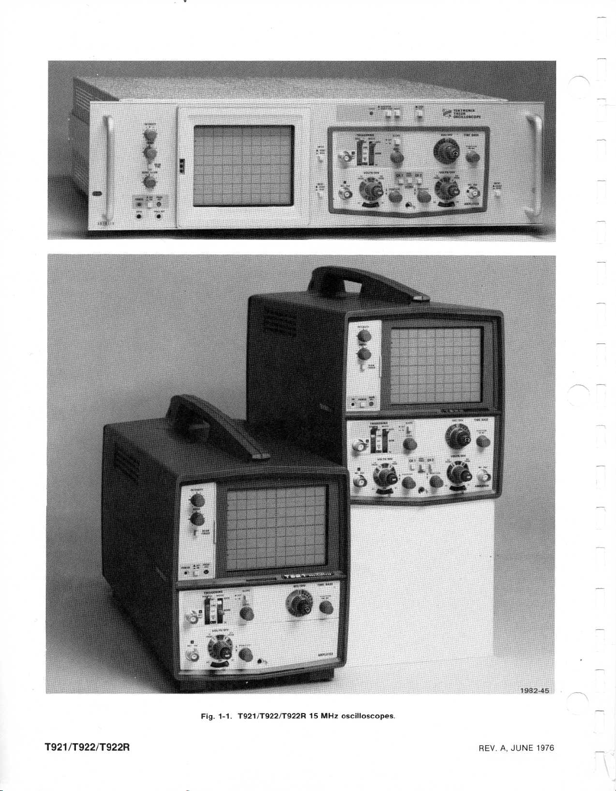
Fig.1-1
.
T921/T922/T922R15
MHz
oscilloscopes
.
REV.A,
JUNE
197
6
Page 8

This
manual
and
T922R
dual
trace,
trace
oscilloscope
traceordual
from2mV
triggering
Amplifier(s)
0.5s/divto0.2Ns/div
extends
cilloscope
Probe
Z-Axis Input
Power
the
The
T992R
Characterist
Adjust
Voltage
+40°
C)
Repetition
Sensitivity
Signal
T921
T922R
Usable
Range
Maximum
Voltage
Input
Source (T922R
Line
Voltage
Ranges
120VRange HI-108
240VRange
includes
portable
oscilloscope
.
trace,
to 10
V/div
over
the
provides
and
maximum
is
a
which
ic
Output
(0°Cto
Rate
Polarity
and
T922
Frequency
Input
Impedance
(ac,rms)
oscilloscopes.The
The
provides
rackmount
takes
SPECIFICATIONS
instructions for
and
the
T921isa 15
Vertical
The
.
full
.AvariableX1to
sweep
A.DISPLAY
Approximately
Approximately1kHz
5
volt
decreaseinintensity
Positive
Either polarity of
applied,
jumper
Dcto5
30
1
kHz
Approximately
HI-LO
nally
LO-90
HI-216
LO-198
Amplifier,
calibrated
TimeBase
bandwidth
calibrated
rateto20
verisonofthe
5-1/4
inches
PerformanceRequirement
signal
going
depending
connections
MHz
V
(dc+peak
or
less
120
adjustments
accessible)
to
to
110V.
to
to
the
T922isa
deflection
provides
of
sweep
ns/div
of
0
.5
causesanoticeable
from
.
ac)30V
.
10
kit
V-240
.
132V.
V
.
250
242
V
.
T921,
MHz,
either
the
rates
X10
.
rack
V
.
.
.
ground
signal
upon
.
.
V
Range
are not
T922
MHz,
15
single
single
factors
stable
Vertical
from
magnifier
T922
os-
space
TABLE
.
can
internal
p-p
and
exter-
Features
sweep;rear
and
user
switch-selectable
CH1,CH
ambient temperature
otherwise
4,
T922R
1-1
.
1-1
Electrical
Line
Maximum
Consumption
CRT
be
Deflection
at
addedtothe
panel
Vertical
selectionofthe
The
when
.
Characteristic
Frequency
Display
Display
Trace
Range
Standard
Phosphor
Nominal
erating
Range
Accuracy
+20°Cto
+30°
O'Cto
Uncalibrated
(VAR)
Signal;internally
and
2,
following
specified
performed
meet
to
Power
Area
Rotation
Accel-
Potential
Factor
C
+451C
Range
Section
rackmount
outputs
CHOP
front-panelorrear-panel
EXT
TRIG
instrument
range
The
Adjustment
.
completely,
the
electrical
150to
36 W,0.35Aat
8 x 10cm.
Adequate
horizontal
P31
12,400V.
B.VERTICAL
mV/divto10
2
2-5
Within3%.
Within4%.
Continuously
settings.Extends
to at
1-T921/T922/T922R
version
for
Sweep
selectableZAxis
ALT
or
PerformanceRequirement
.
sequence
least
dual
signals
60 Hz
.
specifications
0°C
of
allows
specifications
.
to
center
AMPLIFIER
V/div
25
include:single
Sweep
Gate,
trace
to
+45°C
ProcedureinSection
the
listed
60 Hz,
align
line
V/div
;12stepsina
.
variable
deflection
(at
polarity
modes;and
inputs for
apply
over an
T921/T922/
in
120Vline
trace
.
between
least2.5
Ramp,
unless
Table
with
factor
:1)
;
.
1-
.
REV.C
APR
1977
Page 9

Specifications-T921
Chara
cteristic
B.VERTICAL
Frequency
Response
Bandwidth
Risetime
ChoppedMode
Repetition
Rate
(T922)
Input
Resistance
Input
Capacitance
(T921
and
T922)
Input
Capacitance
(
T922R
)
CH
1
and
CH
2,
(front
only)
Maximum
Input
Voltage
DC
Coupled
AC
Coupled
Vertical
Output
(T922R)
Amplitude
High
Im-
pedance
Load
50S2Load
Bandwidth
/T9~2/T922R
Performance
AMPLIFI
Dc
toatleast15MHz
reference
ly
signal
from
VOLTS/DIV
calibrated detent)
23 nsorless
Approximately
Approximately
Approximately
Approximately
400V(dc
+
800V(p-p
400V(dc+peak
800V(p-p
At
least0.5V/divofdisplay
Approximately
play
.
ER
(co
a 25
VAR
.
250
1MO.
30 pF
40pF.
peak
ac)at1
ac)at1
50
Requirement
centered
S2
.
ac)
ac)
Approximately1MHz
TABLE
nt)
(5
division
vertical-
source
control
kHz
.
.
.
kHz
or
less
.
kHzorless
.
mV/div
of
.
with
.
.
dis-
in
1-1
(cont)
Characteristic
Sweep
Calibrated
Accuracy
+20°Cto
+30°
O'Cto
Variable
Magnifier
X-Y
Operation
Deflection
Variable
Magnifier
X-Axis
T921&T922
T922R
Input
Input
T921
T922R
Phase
Between
Y-Axis
Rate
Range
C
Unmagnified
Magnified
+45°
Unmagnified
Magnified
Factor
X10
X1
Bandwidth
Resistance
Capacitance
&T922
Difference
X-
and
Amplifiers
PerformanceRequirement
C.TIME
0.5s/divto0
1-2-5
magnifier
sweep
Accuracy
BASE
.2,us/div;20 stepsina
sequence.VariableX1to
extends
rate
to20ns/div
specification
over center8divisions.Exclude
first
50
ns
of
sweep
magnified
rates
100th
and
and
anything
magnified
unmagnified
beyond
division
Within3%.
Within5%.
C
Within4%.
Within6%.
Approximately
Approximately
DC
toatleast1MHz
reference
DC
to
least1MHz
reference
Approximately1MO
Approxiamtely
Approximately
only)
.
5°
or
less
100 mV/div
1
V/div
signal
.
signal
.
.
30 pF
.
40 pF
(front
fromdoto50kHz
X10
maximum
.
applies
for
both
sweep
the
.
.
.
with10div
with5div
input
.
REV.B,
DEC
.
197
6
Page 10

Specifications-T921
/T922/T922R
Performance
_
Char
acteristic
Triggering
Sensitivity
TV
Sync
External
Trigger Input
Maximum
Voltage
Input
Resistance
Input
Capacitance Approximately
(T921
and
Input
Capacitance
(T922R,
Level
Range
EXT
EXT
10
Characteristic
Temperature
Storage
Operating
T921&T922
T922R
Input
T922)
front
C
TABLE
TIME
.
1-1 (cont)
BASE
0.5div
from2Hzto1
1.5div
MHz
at
15
Composite
100
mV
2.3divor230
video)
.
400V(dc+peak
800V(p-p
Approximately1Mfg
Approximately
only)
+0.5Vto-0.5V
+5Vto-5V.
TABLE
Environmental
Performance
-550Cto+750C
0°Cto
0°Cto
Requirement
(cont)
internalor100
MHz,
internalor150
.
sync1div
external
(approximately
mV
ac)
ac)(1kHzorless)
30 pF
40 pF
.
1-2
Requirement
.
+45°C.
+50°C.
mV
external
increasing
mV
external
internal
of
composite
.
.
.
.
TABLE
Characteristic
1-2 (cont)
PerformanceRequirement
Altitude
Storage
Operating
to
To
50,000ft.
To
15,000ft.
temperature
ft.above
5,000ft.
Maximum
decreases
operating
1°C/1,000
or
TABLE
1-3
Physical
.
Characteristic
PerformanceRequirement
Weight
T921
and
T922
With
Panel
15.5Ibs(7.0
kg)
.
Cover,
Accessories
and
Accessory
Pouch
Without
Panel
15.0lbs.(6.8kg)
.
Cover,
Accessories
and
Accessory
Pouch
T922R
kg)
Without
19.0Ibs(8.6
.
Accessories
Domestic
Shipping
Overall
(T921
Overall
(T922R)
Dimensions
and
T922)
Dimensions
Wt
33.0Ibs
(15.0kg)
RefertoFig.1-3
RefertoFig.1-2
.
.
.
REV.B,
DEC.197
6
Page 11
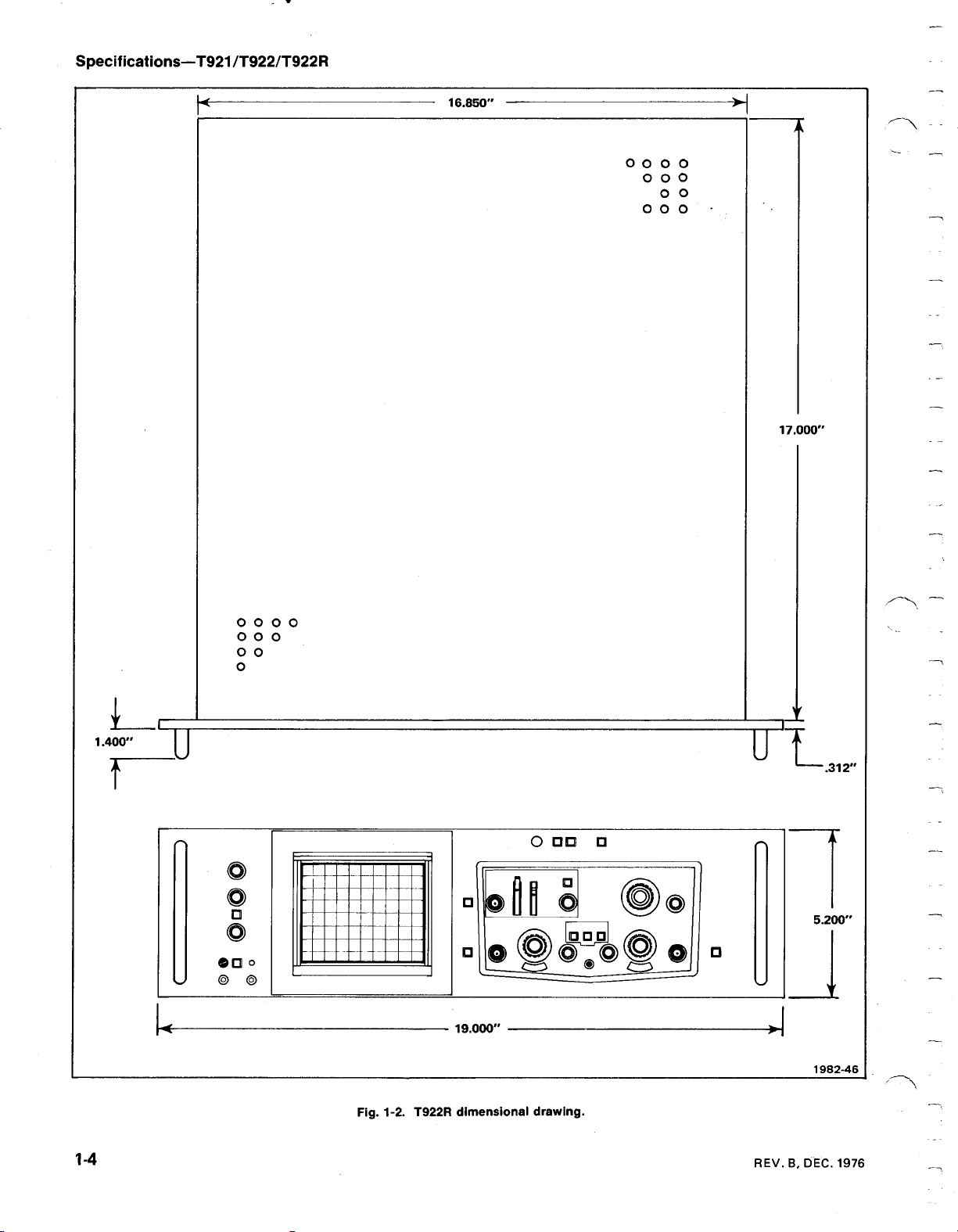
Specifications-T921
/T922/T922R
Fig.1-2.T922R
dimensional
drawing
.
REV
.
B,
DEC.197
6
Page 12
Specifications-T921
/T922/T922R
STANDARD
1
Instruction
1
Probe
2
Probes
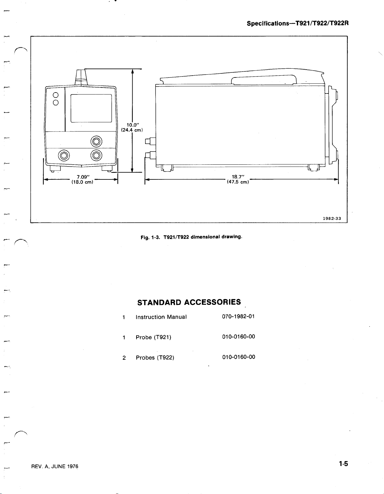
Fig.1-3
T921/T922dimensional
.
ACCESSORIES
Manual
(T921)
(T922)
drawing
.
070-1982-01
010-0160-00
010-0160-00
REV.A,
JUNE
1976
1-5
Page 13

Specifications-T921
RECOMMENDED
The
following
our
catalog
are
listedasa
measurement
prices,
contact
COVERS
FRONT
during
transport
accessories
match
the instrument
Order
cover
during
Order
floor
viewing
accessories
. ... . . . . . . . . . . . . . . . . . . . .
PROTECTIVE
provides
transport
. . . . . . . . . . . . . . . . . . . .
STAND
PORTABLE
and
holds
and
accessories
specifically
needs.For
refertoa Tektronix
your
local
COVER:Protects
or
(probes,
protection
or
STAND:The
the instrumentatan
access.Also
(probe,
/T922/T922R
NOTE
convenience
Tektronix
storage
WATERPROOF
storage
cables,
case
cables,
and
.
.
ACCESSORIES
have
been
selected
for
your
instrument.They
to
help
you
detailed
the instrument
etc.)Madeofblue
for
Portable
provides
etc.).
information
Products
Field
provides storage
COVER
the
. . ... .
Catalog
Representative
. .
entire
Stand
angletoprovide
storage
from
meet
your
and
or
.
front
panel
forsmall
plastic
016-0340-00
:
Blue
vinyl
oscilloscope
016-0361-00
sitsonthe
easy
for
small
to
P6015
GENERAL
Provides
struments
input
Order
P6021
from
instruments
inches)toallow
the
Order
P6006
The
compensation
match
bandwidthofthe
bandwidthofthe
Order
CAMERAS
with
batteries
version
ture
tion.Mechanical
bulb
full
bandwidth
.
Can
capacitance
. . . . . . . . . . . .
AC
CURRENT
120
Hz
to
.
Spring-loaded
circuit
C-5A
under
. . . . . . . . . . . . . . . . .
GENERAL
P6006isa
rangeofthe
the
front
. . . . . . ... . .
Option3Camera
xenon
f/16
and
flash
.
Recommended
T900-series instruments.Fixed
lens
with0.67
time
.
PURPOSE
capabilities
be
compensated
.
. . . . . . . . . . . . . .
PROBE:Provides
the
upper
measurement
test
.
PURPOSE
10X
do
to35MHz
inputsofthe
P6006
allows
T922R
.
. . . . . . . . . . . . . . .
:
lamp
powered
for,
or 0
shutter
with
1000X
VOLTAGE
of
T900-series
to
match
bandwidth
slide
of
current
. . . . . . . .
10X
P6006
T922R.The
full
useofthedcto 15
Provides
and
moldedtofit
.85
user
speedsof1/5to1/25
of
opens
without
VOLTAGEPROBE
voltage
allows
adjustment
doto35
graticule
by
two
focus,
adjustable
PROBE
the
vertical
010-0172-00
a
bandwidth
T900-series
(up
to
0
.150
breaking
.015-0140-02
probe.The
MHz
MHz
010-0160-00
illumination
AA
penlight
all
bench
fixed
aper-
magnifica-
s,
plus
:
in-
:
to
Order
PROBES
Input
capacitance)
Order..........
Provides
struments.Can
input
Order
Provides
struments.Can
input
Order
. . . . . . . . . . . . . . . . .
P6101
GENERALPURPOSE
capacitance
.
P6062A
P6009
SWITCHABLE
full
bandwidth
capacitance
. . . . . . . . . . . . . . . .
GENERAL
full
bandwidth
capacitance
. . . . . . . . . . . . . . . . .
. . . . . . .
1X
VOLTAGE
54
picofarads
. . ... ...................
capabilities
be
compensated
.
PURPOSE
capabilities of
be
compensated
.
(plus
1X-10X
to
. . . . . . . . .
100X
to
. . . . . . .
VOLTAGE
VOLTAGE
match
. . ... .
oscilloscope
.010-6101-03
of
T900-series
match
the
.010-6062-13
T900-series
the
.
.
010-0264-01
. .
209
PROBE
input
PROBE
vertical
PROBE
in-
vertical
:
in-
:
Order
T922R
:
The
graticule
T922R
CAMERA
C12,
C27,
C30A,Order
C59,
RACKMOUNT
T922Rina
Order
. . . . .
C-5A
Option1Camera
.
Option1deletes
T922R
The
Order
Order
Order
Provides the
is
flash
following
using the
rack
. . . . . . . . . . .
. . .
. .
. . . . . . . . . . . . . .
:
Recommeded
the
graticule
equipped
unitisnot
cameras
listed
..... . .
. . . . . . .
. . . . . . . ... . . .
. . . . . . . . . . . . . . . .
HARDWARE
slides
.
with
scale
necessary
are
also
adapter
. . . . . . . . . . . . . . .
. . . . . . . . . . . . . . .
and
. . .
.
KIT
hardware
. .
. . . . . . . . .
. . . . ... .
C-5A
Option
for
use
with
the
flash
unit
from
C5A
illumination,sothe
.
compatible
. . . . ..016-0249-03
neededtomount
with
ADAPTER
01,6-0299-00
016-0249-03
016-0248-00
016-0375-00
.
the
the
3
.
REV.C
JUL
197
7
Page 14
Section
2-T921
/T922/T922R
OPERATING
The
T921,
T922,
120Vor
To
selector
bottomofthe
positions
input
the
10%
240
avoid
switch
voltage.The
applied
from
To
avoid
not
attempt
selector
must
be
Vac,50to
equipmentdamage,
instrument
which
power
the value
electric
switch,
done
SAFETY
The
T921, T922,
phasepower
conductors
potential
current-carrying
ground
recommended,
current
source
(the
.
Operation
(suchasphase-to-phaseona
(fuse)
protection
OPERATING
VOLTAGE
and
T922R
60Hznominal
(120Vor
include
POWER
input
for
which
WARNING
shock
to
change
HI1LO
by
qualified
INFORMATION
and
with
neutral
from
conductors
since only the
will
operate
the
240V)and
(T921/T922
the valueofthe
indicator
voltage
switch,orinternal
T922R
within
varies
the switches are
and
equipmentdamage,
the
power
service
operate
one
of
the
conductor)
power
sources
are
live
line
conductorhas
the
instrument
from
power
input
power
HI/LO
only)
lamp
personnel
3-wire
input
switchonthe
mustbe
applied
blink
will
more
than
set
input
fuse.This
fromasingle-
current-carrying
at
ground
where
with
respect
system)isnot
.
either
source
range
set
power
when
about
.
do
range
only
(earth)
over-
INSTRUCTIONS
.
both
to
a
to
.
Front
INTENSITY-Adjusts
play.Set
life
FOCUS-Adjusts
tion
(3)BEAM
presses
independently
signals
To
(Fig.2-1)
Panel
for
the lowest
.
.
FINDER--Locates
the
crt
.
locateanoff-screen
a.Set the
controls
POSITION
b.Ifadisplayordot
BEAM
play
INTENSITY
FINDER
or
to
dot
A.DISPLAY
the
visible
for
optimum
off-screen
display
of
vertical
midrange
control
should
untiladisplay
to
the
position
display
POSITION
and
clockwise
holdin.Acompressed
and
appear.If
brightnessofthe
displaytoprolong
size
spot
within
controlorapplied
:
rotate
.
stillisnot
appears
and
displays.Com-
the
graticule
and
INTENSITY
the
visible,
not,
increase
.
crt
dis-
crt
defini-
area
horizontal
press
dis-
the
The
T921,
T922,
and
terminal
source
is
directly
For
outlet
polarized
and
safety-earth.The
connectedtothe metal
electric-shock
withasafety-earth
protection,
FUNCTIONS
CONNECTORS,
T921
(See
text
preceding
features
from
Before
manualtofamiliarize
tors,
REV.A,
the
you
and
JUNE
found
onlyinT922R
T921/T922
turn
the instrument on, read
indicators
.
1976
T922R
plug
AND
NOTE
FIRST
.)
yourself
havea3-wire
for
connection
ground
insert
contact
OF
CONTROLS,
AND
T922
TIME
with
cord
to
the
terminalofthe plug
partsofthe
this
.
instrument
plugina
INDICATORS
OPERATION
or those
the
controls,
which
this
portionofthe
witha3-
power
mating
for
differ
connec-
the
If
a dotor
triggered.Set the
to
obtain
POSITION
.
0
center
FINDER
trol
forastable
Ifacompressed
VOLTS/DIV
tical
POSITION
PROBE
approximately0.5V(negative-going
ground)atapproximately
voltage
ON-OFF-Push-push
power
on
versions
vertical
display.Use
a
controlstomove
of
the
button
switch
ADJ-Provides
probes
.
(button
this
switch
line
appears,
trigger
graticule.Release
and
display
controls
in)
is
MODE
the
vertical
the
the
adjust
.
display
and
switch turns the instrument
and
labeled
appears,
the
horizontal
for
a
a
square-wave
1
kHz,
off
(button
POWER
sweepisnot
switchtoAUTO
and
horizontal
display
trigger
stable
for
near the
the
level
adjust
and
display
output
respect
with
compensating
out).(In
.)
BEAM
con-
the
ver-
.
of
to
some
Page 15
Operating
Instructions-T921/T922/T922R
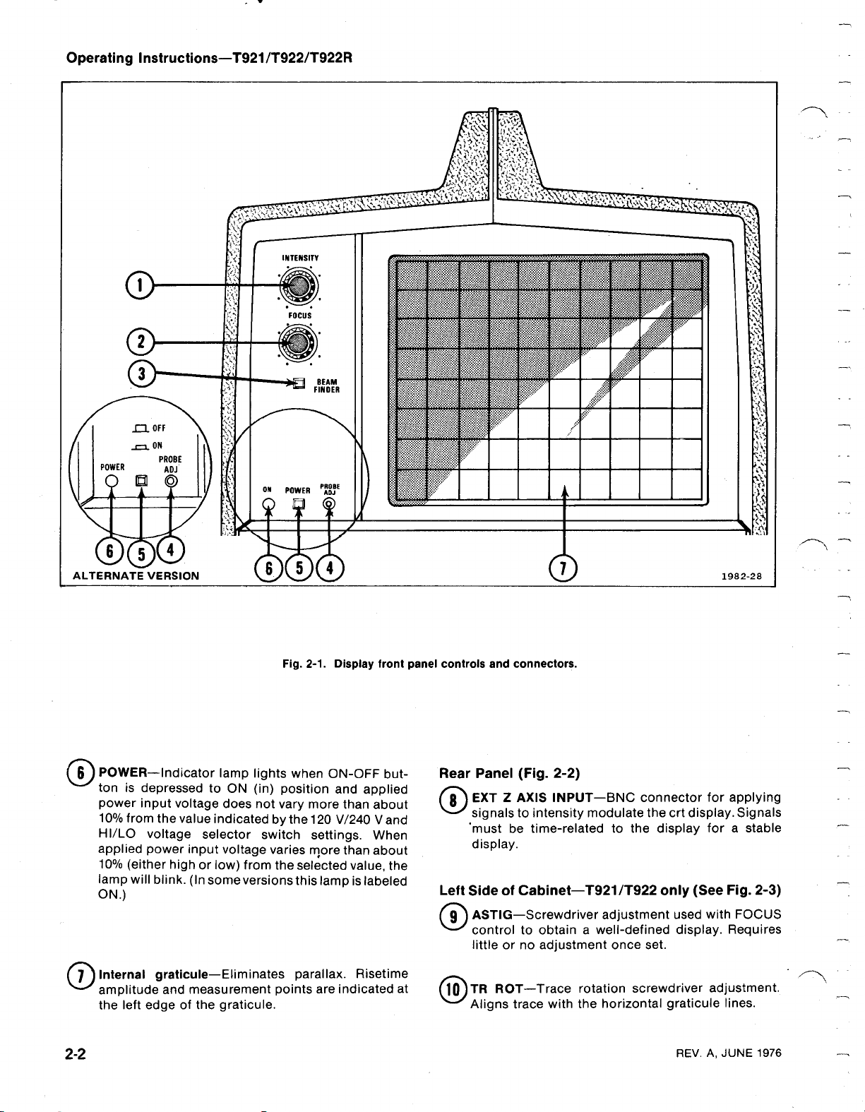
POWER-Indicator
ton
power
10%
HI/LO
applied
10%
lamp
ON
O
Internal
amplitude
the
2-2
is
depressed
input
voltage
from
thevalue
voltage
power
input
(either
highorlow)
will
blink
.
(In
.)
graticule-Eliminates
and
measurement
left
edgeofthe
Fig.2-1.Display
lamp
lights
to
ON
(in)
position
does
not
vary
indicated
selector
voltage
someversionsthis
graticule
from
by
switch
varies
the
points
.
front
when
ON-OFF
and
applied
more
than
about
the
120
V/240Vand
settings.When
more
than
about
selected
parallax.Risetime
lamp
are
indicated
value,
is
labeled
but-
the
panel
at
controls
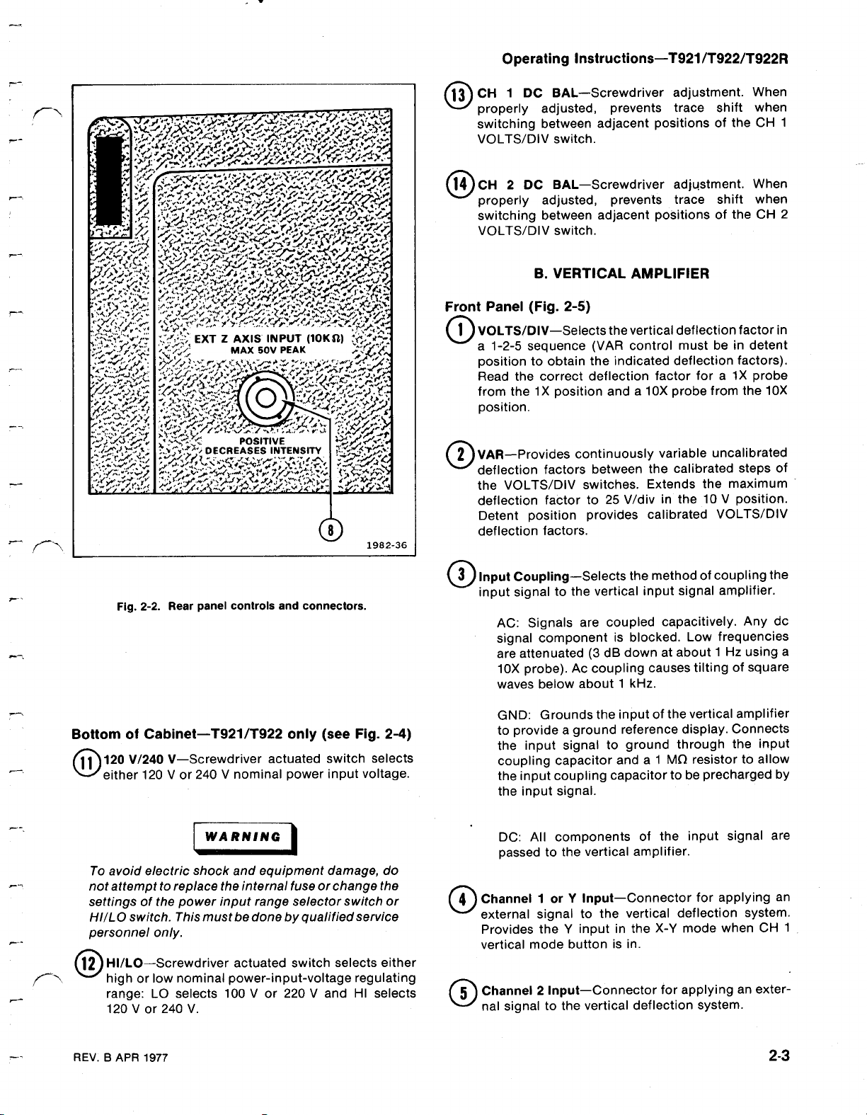
Rear
Left
O
and
connectors
(Fig.2-2)
Panel
Z
EXT
signalstointensity
'must
display
Side
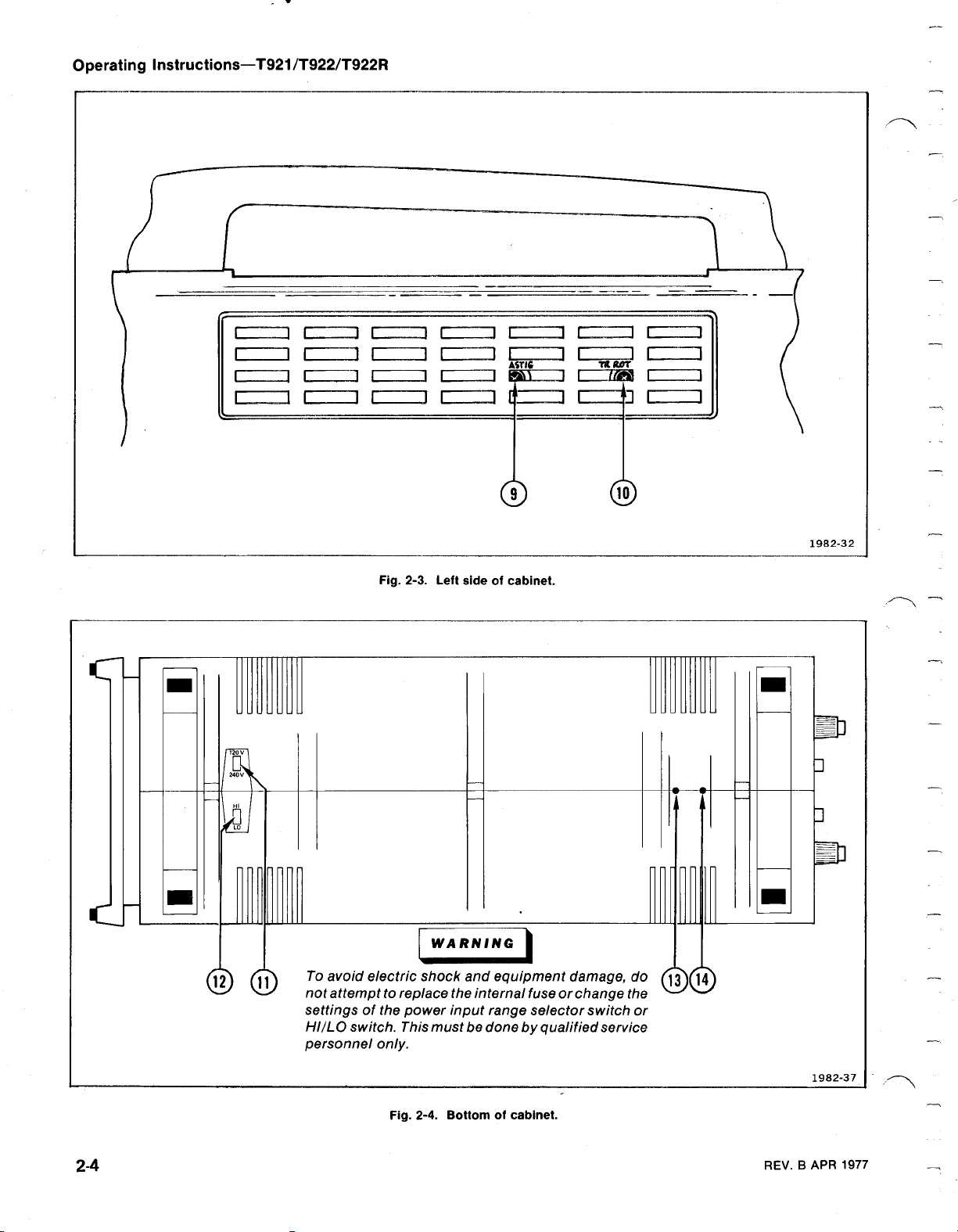
ASTIG-Screwdriver
controltoobtainawell-defined display.Requires
littleorno
TR
Aligns
AXIS
be
time-relatedtothe
.
Cabinet-T921/T922
of
ROT-Trace
trace
.
INPUT-BNC
modulate
adjustment
rotation
with
the
connector
the
adjustment
set
once
screwdriver
horizontal
crt
display.Signals
display
only
(See
used
.
graticule
REV.A,
for
applying
forastable
Fig.2-3)
with
FOCUS
adjustment
lines
.
JUNE
1976
.
Page 16
@
Operating
CH
1
DC
properly
switching
VOLTS/DIV
Instructions-T921/T922/T922R
BAL-Screwdriver
adjusted,
between
switch
prevents
adjacent
.
adjustment
trace
positionsofthe
shift
.
When
when
CH
1
Fig.2-2.Rear
panel
controls
and
connectors
CH
2
DC
BAL-Screwdriver
properly
switching
VOLTS/DIV
FrontPanel
VOLTS/DIV-Selects
O
a
1-2-5
position
Read
from
position
VAR-Provides
O
deflection
the
deflection
Detent
deflection factors
Input
.
input
AC
signal
are attenuated(3dB
10X
wavesbelow
adjusted,
between
switch
B.VERTICAL
(Fig.2-5)
sequence
to
obtain
the
correct
the1Xposition
.
factors
VOLTS/DIV
factorto25
position
Coupling-Selects
signal to
Signals are
:
component
probe).Ac
prevents trace
adjacent
.
the
vertical
(VAR
control
the
indicated
deflection
anda10X
continuously
between
switches
V/divinthe 10Vposition
provides
.
the
the
vertical
coupled
is
blocked
downatabout1Hz
coupling
about1kHz
adjustment.When
positionsofthe
AMPLIFIER
deflection
must
deflection
factor fora1X
from
probe
variable
calibrated
the
Extends
.
calibrated
methodofcoupling
input
causes
.
the
signal
capacitively.Any
Low
.
tiltingofsquare
shift
when
CH
factor
beindetent
factors)
probe
the
10X
uncalibrated
steps
of
maximum
VOLTS/DIV
the
amplifier
frequencies
.
do
using a
2
in
.
.
Bottom
@
@
of
Cabinet-T921/T922
120
V/240
either
120Vor
To
avoid
not
attempttoreplace
settings
HI1LO
personnel
of the
switch.This
HI/LO-Screwdriver
high or
range:LO
120Vor
REV.B
APR
1977
V-Screwdriver
electric
shock
power
only
.
low
nominal
selects
240V.
actuated
V
nominal
240
WARNING
and
equipment
the
infernal
input
range
mustbe
done
by
actuated switch
power-input-voltage
100Vor
220 V and
only
(see
switch
power
input
damage, do
fuseorchange
selector
switch or
qualified
selects
Fig.2-4)
selects
voltage
.
the
service
either
regulating
HI
selects
Grounds
GND
:
to
provideaground
the
input
signal
coupling capacitor
the
input
coupling
the
input
signal
DC:All
passed
Channel
external
Provides theYinputinthe
vertical
Channel2Input-Connector
O
nal
signal to
components
the
to
1 orYInput-Connector
signal to
mode
button
the
the
inputofthe
reference
ground
to
anda1
capacitortobe
.
vertical
the
vertical
isin.
vertical
display.Connects
through
Mil
of
the
amplifier
deflection
X-Y
mode
applyinganexter-
for
deflection
vertical
the input
resistor to
precharged
input
signal
.
for
applying
when
system
amplifier
allow
by
are
an
system
CH
.
2-3
.
1
Page 17
Operating
Instructions-T921/T922/T922R
U
12
say
~
~II
-
III
settings
HI1LO
personnel
Fig.2-3.Left
of the
power
switch.This
only
.
sideofcabinet
WARNING
input
range
mustbedoneby
.
selector
qualified
S
switch
service
II
WOMM
or
III
1982-32
U
2-4
Fig.2-4.Bottomofcabinet
19
82-37
.
REV.B
APR
1977
Page 18

PRO
AC
VOLTS/DIV
tx
og
\O6
'wm
GRD~~
/S
Fig.2-5.Vertical
tox
PROBE
N
Operating
TRACE
CH
TRIG)
2
front
panel
CH1DUAL
POSITION
DC
(CHI
S
amplifier
VOLTS/DIV
Ix
PROBE
AC
~t75
controls
Instructions-T921/T922/T922R
FA
0
tox
PROBE
1,z
S
RAO
30DF
\
W
GOOD
DC
AMPLIFIER
.
t
1982-11A
O
POSITION-Controls
display
O
Vertical
operating
CH1:
input
for
CH2:
input
DUAL
signals
selected
For
Chopisselected.For
Alternateisselected.In
trigger
DUAL
the
(insteadofCH1)while
displayed
.
Mode-Selects
mode
.
Displays
connector.This
X-Y
operation
Displays only
connector
TRACE:Displays
alternately.Chop
automatically
SEC/DIV
switch
signalisderived
TRACE
same
time,
and
the
.
the
vertical
the
only
signal
button
.
signal
.
by the
settings
settingsof.5
DUAL
CH2buttons
trigger
DUAL
positionofthe
vertical
appliedtothe
mustbe
appliedtothe
CH1and
or
Alternate
SEC/DIV
of1ms
TRACE
from
CH1.
are lockedinat
signal
comes
TRACE
CH
and
ms
amplifier
latched
2
mode
switch
slower,
faster,
and
mode,
When
from
signals
crt
CH
CH
input
the
the
CH
are
in
is
TIME
BASE
the
sourceofthe
of
signalinthe
TRACE
CH1.IfCH
latched
the
mode,
in,
signal
2and
trigger
signal
displayed
CH1or
the
trigger
signal
DUALTRACE
channel2is
CH
.
on
2
the
Front
Panel
SOURCE-Selects
C
.
(Fig.2-6)
INT:Usesasample
the
crt
as a
trigger
modes.In
is
obtained
DUAL
from
buttons are both
trigger
source
.
1
signals
signal
10
of
sampleofthe
a
signal
.
triggering
trigger)
must
forastable
trigger
.
Line
:Uses
a
trigger
as
EXT
:Permits
X
2
(external
trigger
played
EXT=10:External
factor
power-line
signals
on
input
connector.External
be
time-relatedtothe
display
frequency
appliedtothe
.
signalisattenuatedbya
dis-
.
X-Y:Permits x-y
through
is
(vertical
For
2
obtained
button
(DUAL
theXinput
normally
mode
special applications,
from
latched
TRACE
display.X
through
CH1button
the
in),orfrom
button
(horizontal)
connector.Y
theCH1
orY
mustbelatched
theYinput
CH2input
both
latched
(vertical)
input
connector
connector
1
and
CH
in)
.
input
input
may
(CH
CH
in)
be
is
.
2
2
REV.A,
JUNE
1976
2-5
Page 19

Operating
Instructions-T921/T922/T922R
I
LIMODE-Selects
circuit
.
AUTO:With the
the
sweep
repetition
absenceofan adequate
the
LEVEL
runstoprovide a reference
NORM:Permits
In
the
when
sweep
Setting
adequate
TV:Permits
TriggersonTV
at.1ms
SEC/DIV
SLOPE
signals
signals
(SLOPE-Selects
slopeofthe
the
operating
proper
canbetriggered
rates
above
controlismisadjusted,
triggering
absenceofan
the
LEVEL
does
not run
SOURCE
trigger
triggering
or
slower.Triggers
switchisset
switchto+OUT
and
to
.
trigger
adequate
controlismisadjusted,
and
to
LINE
signal
field
when
-IN
the
positive-ornegative-going
waveform
Fig.2-6.Time
mode
LEVEL
by
trigger
about
trigger
display
on
no
position
.
on
television
SEC/DIV
at
50Nsor
for
sync-positive
for
sync-negative
.
base
front
for
the
trigger
control
20Hz.
signal,orwhen
displayed
trigger signal,
displayisvisible
on
setting,
signals
the
.
provides
switchisset
TV
faster.Set the
sweep
signals
line
with
In
the
free
signal
the
when
input
input
or
an
.
.
.
panel
controls
(X
and
connectors
-IN:The
negative-going
LEVEL-Selects
signalatwhich
adjusted
SOURCE
(External
trigger
SEC/DIV-Selects
sequence.X1-X10
detent
rates
numerals
microseconds/division,
underneath
ds/division,
numerals
X1-X10-Provides
(fully
gain
sweep
the
and
signalsorforXaxis
position
directly
withNunderneath
indicate
ccw)
by a
factorof10,
rate
SEC/DIV
.
sweep
for
SLOPE
Trigger)-Provides
indicate
positions
detent
in
the
knob
can
portionofa
the
amplitude
the
sweep
the desired display
have
calibrated
variable
(fully
ccw)
from
the
sweep
with
sweep
ratesinseconds/division
calibrated
position.Increases
providingatleast
X10
detent
set
to.2/is
be
triggered
trigger
pointonthe
is
triggered
been
selected
input
signalsinthe
sweep
control
to
mustbein
read
calibrated
SEC/DIV
indicates
numerals
ratesinmillisecon-
no
symbol
sweep
position
.
signal
after
for
X-Y
ratesina
knob.Knob
sweep
with
under
rates
wheninX1
the
horizontal
(fully
from
20
.
trigger
.
Usually
trigger
.
external
mode
1-2-5
the X1
sweep
rates
the
ns/div
cw)
with
the
.
in
rn
.
2-6
+OUT
:
The
positive-going
sweep
portion
can
be
ofatrigger
triggered
signal
from
.
the
(POSITION-Controls
crt
display
.
the
horizontal
positionofthe
REV.B
APR
197
7
Page 20
-
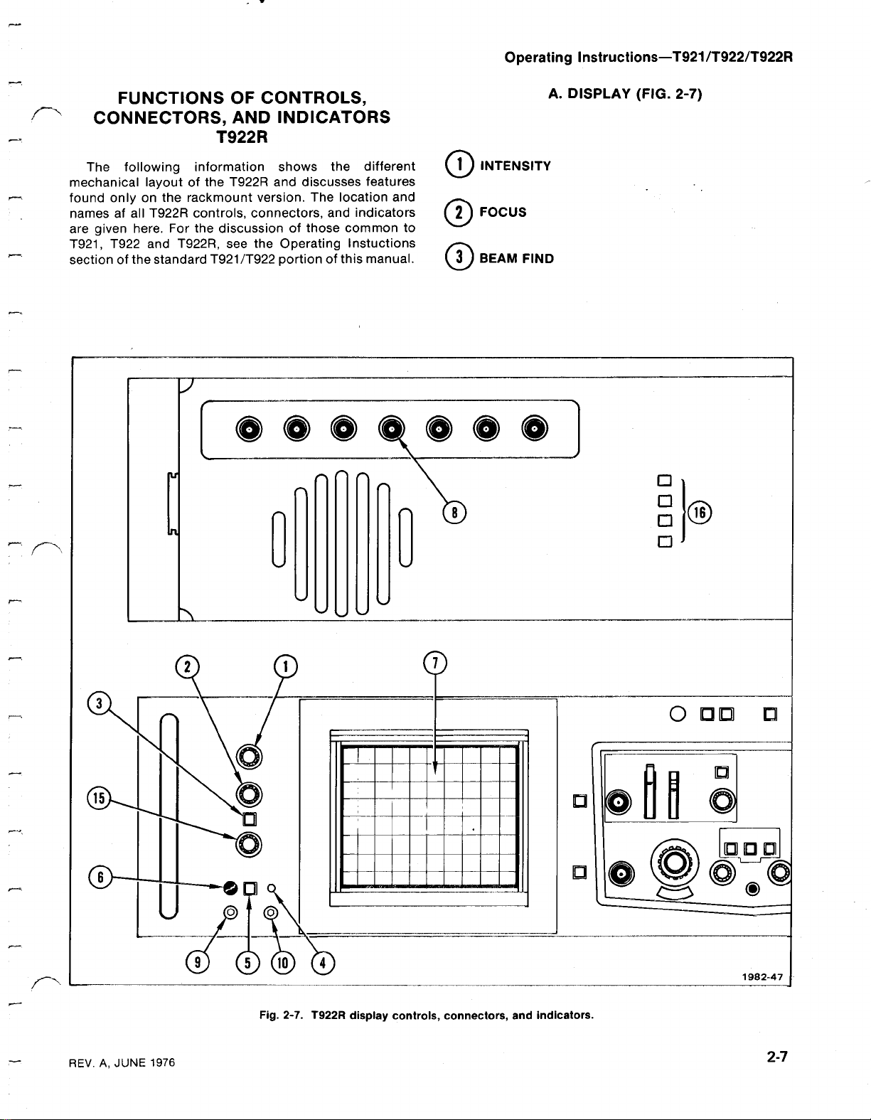
FUNCTIONS
CONNECTORS,
The
following
mechanical
found
names
are
given
T921,
sectionofthe standard
layout
of
onlyonthe
of
all
here.For the discussion
T922
T922R
and
rac
T922R,
OF
AND
T922R
information
the
T922R
kmount
controls,
see
T921/T922
000
CONTROLS,
INDICATORS
shows
and
discusses
version.The
connectors,
those
of
the
Operating
portionofthis
the
different
location
and
indicators
common
Instuctions
O
features
and
to
manual
.
-oo~
Operating
INTENSITY
FOCUS
BEAM
FIND
Instructions-T921/T922/T922R
A.DISPLAY
(FIG.2-7)
rn
vEEN
D
NE
L
EN
LEN
nom
inNNEN
M
a
"
em
01
0
0
®®
13
A]I.
REV.A,
JUNE
1976
O
Fig.2-7.T922R
display
controls,
connectors,
and
indicators
1982-47
.
2-7
Page 21

Operating
Instructions-T921/T922/T922R
(DOFF-ON
O
0
(8
OASTIG
0
@1@1@1
are
internally
PROBE
POWER
Internal
)ZAXIS
TRACE
ADJ
Lamp
Graticule
IN
ROT
and
accessible
WARNING
only
-In
(DChannel
applying
the
OPOSITION
O
Vertical
TRACE
CHOP
CHOP-ALT-Selects
O
modes.Use
at
O
COMP
connectorisa
the
T922R
these
controls
.
displayed
the
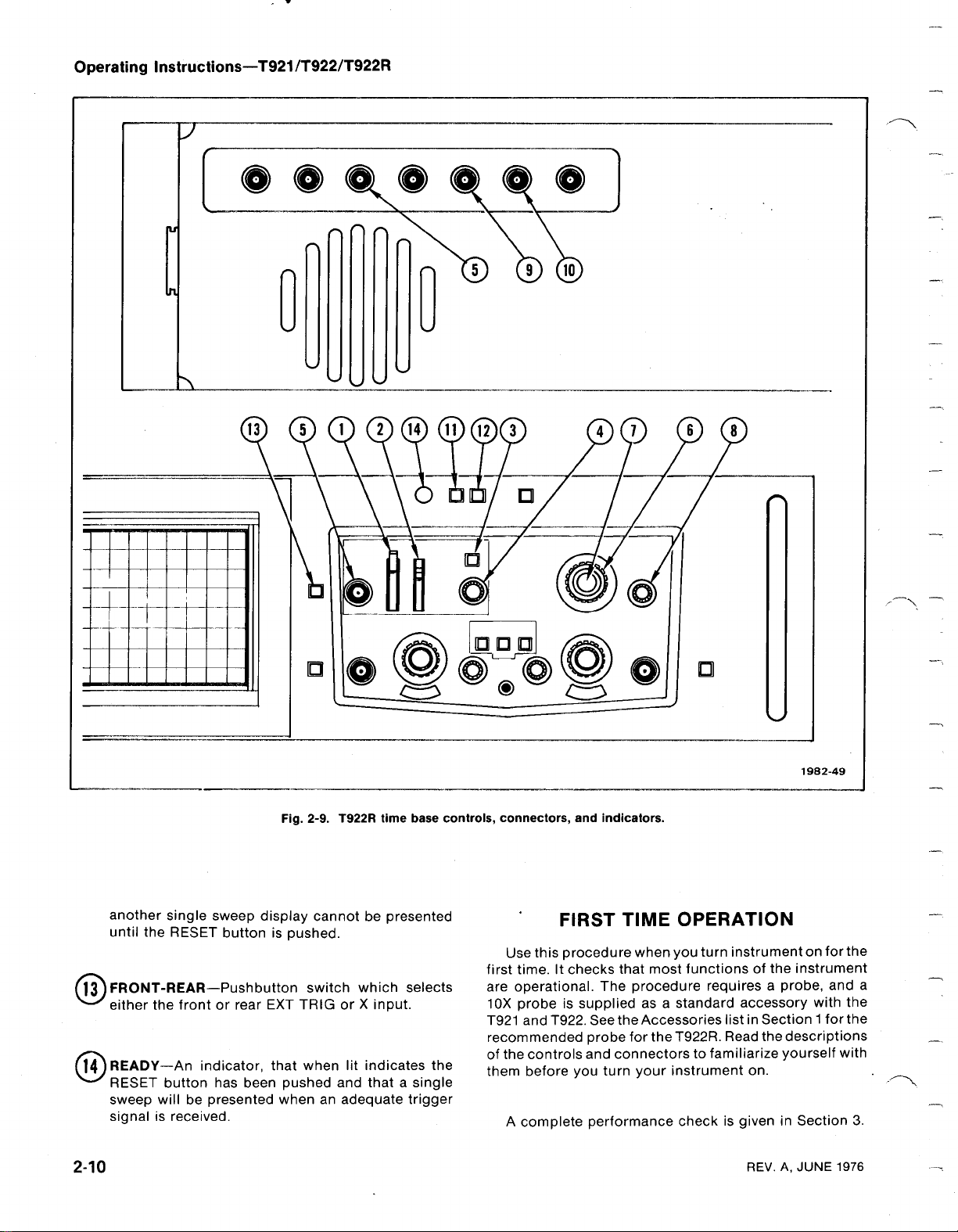
FRONT-REAR-Two
CH1and
or
front
or
higher
VERT
vertical
the
rear
2
Inputs-Two
signalstoChannel2.
panel
and
Mode-When
mode
you
ALT
(see
CHOP
sweep
speeds
SIG
sampleofthe
plusado
positionofthe
one
forCH2,
vertical
switch-selectable
the otheronthe
operating
must
manually
control
at
OUT-The
component
inputs
8)
either
CHOP
lower
sweep
.
display
push-button
which
.
inputs
One
is
mounted
rear
panel
in
the
select either
.
ALT
or
dual
speeds
signal
vertical
proportionaltothe
.
switches,
select either
and
availableatthis
signal
the
DUAL
being
one
for
on
.
trace
ALT
for
front
To
avoid
not
selector
must
@
O
OVAR
electric
attempt
switch,
be
done
SCALE
AC
RMS
the
T922Rissettooperate
B.VERTICAL
VOLTS/DIV
Input
Coupling
shock
to
change
HI1LO
by
qualified
ILLUM
RANGE-Indicates
O
O
Channel1orYInputs-Two
puts
for
applying
mounted
panel
on
the
.
and
equipmentdamage,
the
power
switch,orinternal
service
AMPLIFIER
signalstoChannel1.
front
panel
personnel
the
voltage
.
(FIG.2-8)
switch-selectable
and
the
input
range
fuse.This
only
from
One
otheronthe
do
.
which
rear
in-
is
O
O
O
(D
O
SOURCE
MODE-To
modes
mustbe
SLOPE
LEVEL
EXT
TRIG
external
the
front
SEC/DIV
X1-X10
POSITION
C.TIME
the
settoREPETITIVE
or
triggerorX
panel
BASE
use
the
SINGLESWEEP/REPETITIVE
X-Two
and
(FIG
AUTO,
switch-selectable
signals.Oneismounted
axis
the otheronthe
.
NORM,
(out)
2-9)
.
or
rear
TV
SYNC
button
inputs for
on
panel
.
2-8
REV.A,
JUNE
1976
Page 22

Operating
Instructions-T921/T922/T922R
O
0
REV.A,
SWEEP
responding
crt
.
SWEEP
which
goes
and
goes
JUNE
RAMP
to
GATE
high while
low
1976
Fig.2-8.T922R
OUT-Provides
the
sweep
OUT-Provides
during
retrace
waveform
the
a
ramp
a
logic
crt
traceisbeing
and
holdoff
vertical
appliedtothe
amplifier controls,
output
level
cor-
output
swept
.
connectors,
REPETITIVE/SINGLE
SWEEP
the
when
the
RESET-When
and
and
pushbuttontotheinpositiontooperate
single
sweep
an
adequate
sweep
generator
afterasingle
indicators
operatinginthe single
SWEEP-Set
mode.In
trigger
runs only
sweep
.
the
signal
display
single
becomes
once.Set
has
the
sweep
been
1982-48
SINGLE
available,
RESET
sweep
presented,
mode,
mode
2-
in
.
9
Page 23
Operating
Instructions-T921/T922/T922R
v
v
NOWNWEEN
LEENNEEN
NEEMEN
Norm
another
until
FRONT-REAR-Pushbutton
@
either
READY-An
RESET
sweep
signalisreceived
single
the
RESET
the
button
willbepresented
No
sweep
buttonispushed
front
or rear
indicator,
has
.
display
EXT
that
been
when
Fig.2-9.T922R
cannotbepresented
.
switch
TRIG
when
pushed
or
and
an
which
X
lit
indicates
that
adequate
time
input
base
selects
.
single
a
trigger
controls,
the
connectors,
and
indicators
FIRST
this
time.It
and
T922.Seethe
controls
before
complete
procedure
checks
probe
and
you
turn
performance
Use
first
are
operational.The
10Xprobeissupplied
T921
recommended
of
the
them
A
.
TIME
when
that
most
procedure
as a
Accessories
for
the
connectors
your
1982-49
OPERATION
you
turn
instrument
functionsofthe
requires
standard
T922R.Read
instrument
checkisgiveninSection3.
accessory
listinSection1for
to
familiarize
on
on
forthe
instrument
probe,
a
thedescriptions
.
and
with
yourselfwith
a
the
the
2-10
REV.A,
JUNE
1976
Page 24

Only
the
control
\
performed
unless
follow
a
steporstartinthe
tell
whetherapartiular
a
T921,
First,
switch
are given.Do
instructedtodoso.
the
sequenceofsteps
use
the
check
and
the
bottomofthe
power
input
voltage.In
Voltage
HI-LO
factory.In
Selector
Range
Selector
Europe
switchisnormally
Selectorisnormally
Your
instrument
from a
power
Only
power
range
240Vpower
input
qualified
input
.
settings
not
middleofa
functionisoperational.If
control
that
HI-LO
cabinet
settings
the
Power
Range
(T921/T922
the
United
switchisnormally
switchisnormally
the
Power
set for
240Vand
set forLO.
may
be
input
voltage
voltage
service
selector
personnelshould
selector
that
affect
the
check
move
the
control
Startatthe
throughtothe
check,
for
beginning
end
you
won't be
Channel1only
Input Voltage Selector
Selector
States
only)
set for
switch
are
set
the
Power
120Vand
set forHIat
Input
Voltage
the
HI-LO
damaged
voltage
switch
ifitis
source
set for
change
switchtoa
being
settings
.Ifyou
able
you
have
.
on
the
for
your
Input
the
the
Selector
Range
operated
with
the
120V.
the
different
and
skip
to
You
should
push
the
increasing
two
bright
You
may
controls
Vertical
1.Set
2.Check
trace
off
between
trace
does
horizontal
Operating
get a
BEAM
the
INTENSITY
dots,
indicates
also
havetoadjust
.
Positioning
:LEVEL
SEC/DIV
X1-X10
vertical
that
the
top
and
oneandtwo
not
POSITION
Instructions-T921/T922/T922R
traceonthe
FINDER
button
crt
screen
and
hold
(clockwise).A
that
the instrumentisoperating
the
FOCUS
and
Horizontal
Operation
mid-range
1
ms
X1
(fully
detent)
mode
theCH1
bottom
divisions
extend
control
POSITION
of the
across
CH
control
screen
the
above
the
screen,
untilitdoes
1
.
center
.
If
don't,
you
in
while
it
trace,orone
and
POSITION
ccw
moves
Leave
the
line.If
move
.
or
.
the
trace
the
the
avoid
To
and
See
for
For
selection
connecting
AC
RMS
When
settoindicate
electric
range
changes
the Service
range
change
the
T922R,
controls
your
RANGE
the
instrument
Information
the
are
instrumenttothe
indicatoronthe instrument
the voltage
mentissettooperate
The
POWER
power
input
highorlow)
and
HI/LO
indicator
voltage
from
selector
the value
WARNING
shock,
to
qualified
refer
instructions
input
voltage
internally
leaves
the
range
.
lamp
varies
more
selectedbythe
switches
.
T922R
input
service
sectionofthis
.
selection
accessible
power
source,
factory,
from
will
than
blink
this
which
when
about
voltage
personnel
manual
and
only
.
Before
check
rear
panel
indicator
the
instru-
the applied
10%
(either
120
V/240
.
range
is
the
2
POSITION
divisions
have
two
line
and
the
and
the
vertical
vertical
that
switch
SEC/DIV
INTENSITY
FOCUS
3.Set
the
CH
bottomofthe screen.Leave
and
and two
4.Set the
should
center
5.Check
the
SEC/DIV
.
6.Set
mode
switchtoCH1.
FOCUS
Adjust
fine
V
line atacomfortable
below
traces
one
below
there are
from
mode
control
the
mode
on the
.
.2psto.5s
switch
and
the
brightness
switch
switch
two
Operation
forCH2.Check
the
moves
the
trace
center
for
crt
screen-one
line
DUAL
tracesatevery
.
to1ms
INTENSITY
level
trace
between
.
TRACE.You
and
controls
.
the
off
the top
above
setting
vertical
that
one
for
the
of
a
If
the
`~
connect
the instrumenton.
SOURCE
.A,JUNE
REV
120
V/240VandHI/LO
the
power
cord plugtothe
Set
to
INT
.
1976
the
switches
trigger
power
MODE
are
properly
source
to
and
AUTO,
set,
turn
and
Trace
Most
PROBE
Rotation
of
ADJ
and
the
remaining
signaltothe inputs
Vertical
checks
Input
.
Operation
require
applying
2-
the
11
Page 25
Operating
In
coaxial
VOLTS/DIV
supplied
window
The
ly
compensated
the
signal
If
Compensation
1.Set
2.Using
with
trace
sideofT921
.with
3.Connect
probe
AC-GND-DC
ly2.5
center
4.Set theCH1
shouldbeapproximately
center
Instructions-T921/T922/T922R
the
following
cable,
.
PROBE
but
wanttocompensateaprobe,
you
:CH1VOLTS/DIV
the
center
rotation (control
the center
tip
against
divisions
line.This
.
line
use
settings.If
with
T921
ADJ
outputisa
probe
will
not
information
1
VAR
CH
CH1AC-GND-DC
the
CH1POSITION
graticule
and
T922)
graticule
the
Probetothe
the
switchtoDC.You
display.The
display
AC-GND-DC
NOTE
steps,ifyou
the
1X
you
and
T922),
square
will
distort
affect
the
after
line.If
the
marked
PROBE
TR
for the
best
line
.
ADJ
square
mayormay
equidistant
use
a 1X
probe
PROBE
usea10X
the top
checks
this
control,
traceistilted,
ROT
CH1input
connector.SettheCH1
should
wave
switch
window
probe
use
the
10X
probe
wave.An
refertothe
procedure
.2V(10X
detent
(fully
GND
on
alignmentofthe
haveapproximate-
notbestable
toAC.
above
and
.
clockwise)
align
the
left-cabinet
and
will
be
The
and
incorrectbottom
.
window)
the
adjust
hold
below
display
below
or
for
(as
Probe
trace
the
trace
the
the
.
the
of
6.Set
:Vertical
CH2VOLTS/DIV
CH2VAR
CH2AC-GND-DC
CH2POSITION
7
.
Connect
probe
tip
8.Set
wave
willbebelow
9.Set theCH2
wave
will
the center
10.Rotate theCH2
display
fully
clockwise
11.Return
X-Axis
1.Connect
available,
control
PROBE
SITY
controlasneededtolocate
dots
control
counterclockwise
fully
2
.
Set
as
separatedbya
the
against
theCH2
be
approximately
line
.
amplitude
the
Operation
the
use
it,ifa
clockwise)
ADJ
connector
the
SOURCE
necessary
setting.Return
Mode
probetotheCH2
the
PROBE
AC-GND-DC
the center
AC-GND-DC
VAR
will
decrease.Leave
(in
detent)
vertical
probetotheXinput
10X
probe
and
.
switchtoX-Y,
.
Adjust
distance
detent)
ADJ
switchtoDC.The
line
switch
equidistant
control
.
mode
switchtoCH1.
is
hold the
the
the
display.You
dependent
X1-X10
.
CH
2
.2
V
detent
GND
To
align
with
graticule
input
connector
.
to
above
through
the
(ifa1X
used,
rotate
probe
and
horizontal
(fully
center
and
AC
.
its
VAR
tip
reduce
should
on
to
cw)
trace
line
hold
.
square
The
square
and
below
range.The
control
probe
the
X1-X10
against
INTEN-
POSITION
see
the
X1-X10
X1
(fully
the
is
the
2
If
you
cannot
from
the
PROBE
your
hand.Change
necessary
thick
that
that
verticalisusable
the
thickening
probe
5.Rotate theCH1
display
fully
clockwise
2-12
to
(vertically)
the
probe
your.body
or other
amplitude
NOTE
obtainadisplay,
ADJ
connector
the
getadisplay.The
trace.A
is
pickingupthe
normally
but
the
does
not
instrument malfunction
VAR
will
decrease.Leave
(detent)-maximum
remove
VOLTS/DIV
thickening
power
picksup.Ifthis
PROBE
occur,
you
control
the
probe
.
Touch
display
ADJ
through
display
the
setting
shouldbea
trace
indicates
line
radiation
occurs,
output
haveadefective
.
its
the
VAR
amplitude
tip
tip
to
if
the
isn't.If
range.The
control
.
X-Y
and
Dual
This
modeisusable with
slower.Set
independent
Astigmatism
1
.
2.Connect
probe
LEVEL
FOCUS
both
Vertical
tal
but the
observeatthe
controls
Set
:SOURCE
tip
against
control
control
horizontally
trace
edges
Trace
X-YorDual
Operation
the
thicknessistypically
"corners"ofthe
Operation
SEC/DIV
and
connect
Trace
probetothe
the
PROBE
for the
for
the
and
shouldbeequally
ADJ
most
stable
display
vertically
operation
CH1input
with
signal
settingsof1msor
signals
over the
as
you
would
.
INT
and
hold the
connector.Rotate the
display.Adjust the
the sharpest
entire
more
than the
sharp.This
.
REV
edges
screen
horizon--'~
is
easier
.CJUL
for
.
to
1977
Page 26

3.Set the
best
defined
focus,
useasmall
(through
defined
4.Rotate the
display
the
INTENSITY
Z
Axis
Ext
Forthe
decrease
increase
T922R,
positive-goingora negative-going
decrease
X1410
1.Note
waveform.Rotate
ADJ
X10and
to
controltoX1
2.Set
display
button
through
the
positive
becomes
3
.Set
at
about
Now
LEVEL
will
move
until
the
INTENSITY
display
cabinet
left
display
.
will
get
Input
T921
orT922
in
intensity,
intensity
the
internal
an
in
intensity.See
Trigger
and
a
display
note
.
SEC/DIV
the
(left-hand
to
+OUT
its
range
(rising)
unstable
the
LEVEL
the
middle
set
the
control
along the
display
If
.
screwdrivertoadjust
sideofT921/T922)
INTENSITY
brighter
controltothe
SLOPE
through
and
Operation
a
positive-going
and
levelofa
plug allows a
Operation
with
the
that
only
to.1ms.Position
edge)
position
The
startofthe
.
slopeofthe
.
control
the
of
buttonto-IN
its
negative
becomes
FOCUS
and
the
display
control
defocus
preferred brightness
a negative-going
low-intensity
Service
several
X1-X10
cycleisvisible.Return
one
on
screen.Set
the
.
Rotate
forastable display
slope
.
range.The
(falling)
unstable
controls
still
appears
the
ASTIG
for the
fully
clockwise.The
(get thicker).Return
will
signal
signal
trace.For
selection
signaltocause
Information
cycles
control
the
display
signal
position
start
slopeofthe
.
of
fully
the
LEVEL
will
until
of
of either
.
the
clockwise
startofthe
the
move
the
that
.
Rotate
the
for
the
out
control
best
level
cause
will
the
PROBE
SLOPE
control
along
display
starts
the
display
signal
of
appear,
.
a
a
a
Operating
8.Set
9.Set
appliedtothe
the
adjust
:SOURCE
The
instrumentisnow
PROBE
An
incorrectly-compensated
greatest
are
measurement
insulated
compensation
adjustment
Set
GND-DC
probe
similartothose
correct
compensation
Fig.2-11
sourcesofoperator
equipped
Probe
the
Connect
tip
probes
screwdriver
compensation
appropriate
switchtoDC,
to
compensation
.
Some
Instructions-T921/T922/T922R
SOURCE
the
MODE
CH1AC-GND-DC
CH1input
switchtoLINE
LEVEL
COMPENSATION
adjustments
with
are
similar
PROBE
three
.
compensated
through
VOLTS/DIV
to
accuracy
adjustment
system
the
probe
the
showninFig.2-11
on
control
ready
.
.
is
and
the
ADJ
The
types
untilatrace
INT
AUTO
AC
to
operate
probe
error.Most
to
access
an
Other
probes
that
to
accomplished
showninFig.2-10
switchto.1V,the
the
SEC/DIV
vertical
connector
.
Adjust the
effectsofincorrect
signals
of
.Ifa
trace
appears
when
signal
is
one
attenuator
ensure
by
input
.
optimum
usingasmall,
hole
may
follows
as
switch
and
touch
Noticeadisplay
probe
are
illustrated
doesn't
of
the
probes
to
the
have
.
:
AC-
2ms.
to
for the
probe
.
is
.
an
the
in
4
.Set the
at
about
5.Set
start
on
will
disappearifthe
6.Set the
display
7.Disconnect
CH1AC-GND-DC
disappear
.
BJUL
REV
LEVEL
the
middleofthe slope
the
MODE
the
negative
should
.
1977
control
switchtoNORM.The
slope.In
LEVELcontrol
SLOPE
start
on
the
button
the
probe
switch
forastable
positive
.
the
NORM
to
from
GND.The
to
display
display
mode
improperly
is
+OUT
the
position.The
slope
.
instrument.Set
that
the
adjusted
trace
starts
should
display
the
should
vertical
.
Peak-to-Peak
measure
To
deflection
setting.(Use
factor of
Example
the
values
probe
:
The
display
VOLTS/DIV
:
Amplitude
APPLICATIONS
Amplitude
the
amplitude
(in
VOLTS/DIV
used
.)
amplitudeis3
switchissetto.5V.
divisionsx0.5volt/division
=3
Measurements
a
of
divisions)bythe
window
to
divisions
Substituting
signal,
VOLTS/DIV
match
(see
multiply
switch
attenuation
2-12)
Fig
.
the
1.5V
=
the
and
given
p-p
2-1
3
Page 27
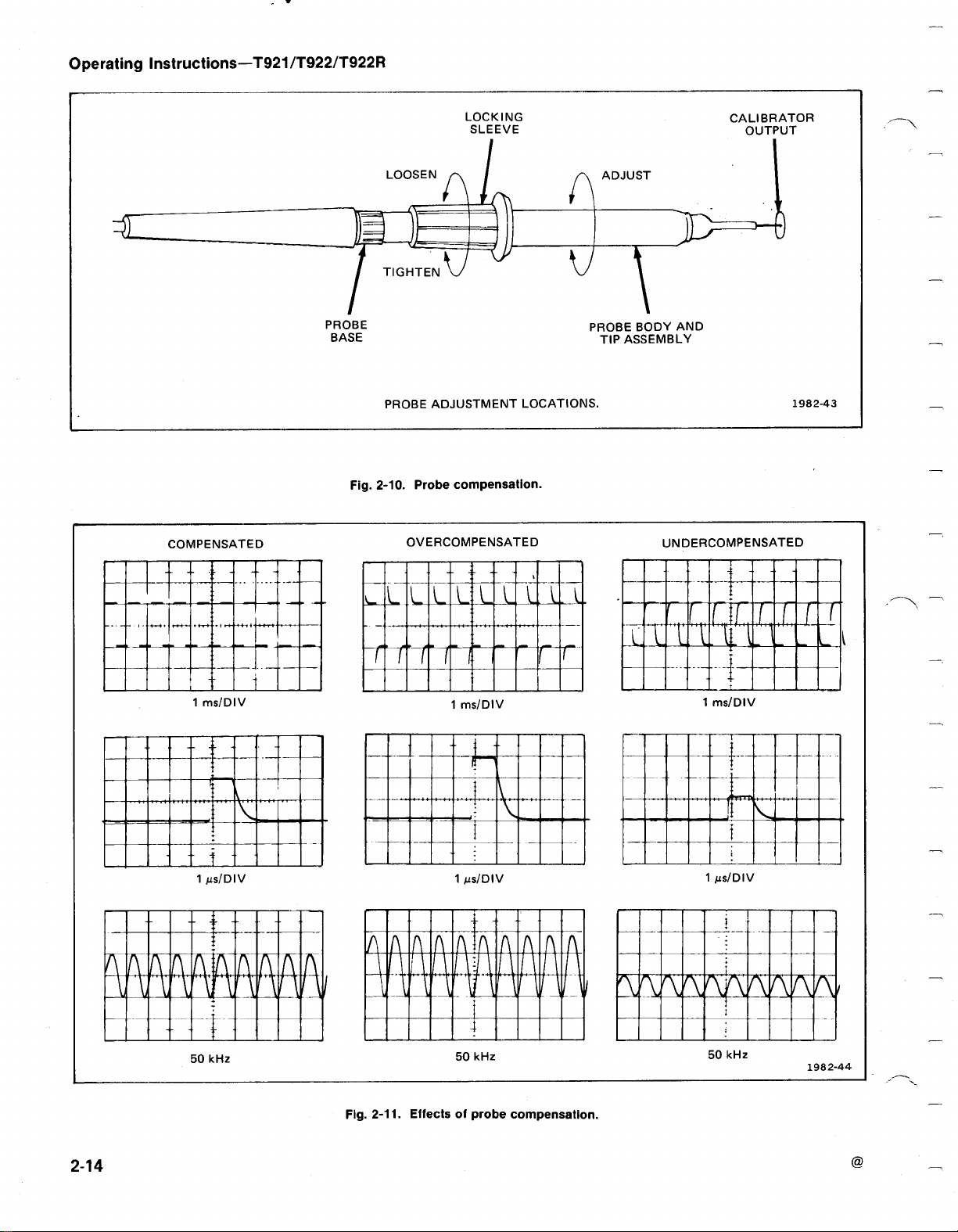
Operating
Instructions-T921/T922/T92211
TTIGHTEN
PROBE
BASE
Fig.2-10.Probe
LOOSEN
PROBE
LOCKING
SLEEVE
ADJUSTMENT
compensation
LOCATIONS
.
I()
ADJUST
PROBE
TIP
.
BODY
ASSEMBLY
CALIBRATOR
OUTPUT
AND
1982-43
COMPENSATED
OVERCOMPENSATED
UNDERCOMPENSATED
III
111
IONE
milli!
MEN
MEN
1
ms/DIV
1
ps/DIV
MMM!q
ONE
,q
A
fA
0
rq,
MMMIMI!M
ms/DIV
1
1
us/DIV
0
MCI!
ON
a
WN
No
INIMMI
1
ms/DIV
1
us/DIV
LKIN
50
kHz
50
kHz
Fig.2-11.Effectsofprobecompensation
50
.
kHz
1982-44
Page 28

5x
6!
11
NOMMIN
o
'Em"O'No
Fig.2-12.Peak-to-peak
Instantaneous
The
following
amplitude
ground
.
of
MEO
N
Amplitude
procedure
any
point
111-
NoNo
low
MEN
voltage
Measurement
expains
onawaveform
VERTICAL
DEFLECTION
measurement
how
to
measure
with
1907-27
.
respect
the
Operating
Substituting
Instantaneous
Voltage
VERTICAL
DIFFERENCE
to
Instructions-T921/T922/T922R
the
given
values
:
__
divisions divisions
Instantaneous
Voltage
=
+50
ON
90
Nil
0
M_
REFERENCE
LINE
10
mV
MOM
ME
-1
mV/
I
-
50
ME
IN!
ENO
1907-28
mV
1.Set
the
AC-GND-DC
2.Apply
vertical
select
3.Obtainastable
4.Set the
tracetosome
5.Set
appears
the
waveform
voltageisnegative
6.Measure
between
waveformand
Example
the
input
connectors.Set the
the
channel
the
AC-GND-DC
above
the reference
:
AC-GND-DC
reference
the
appears
multiplybythe
signal
used
reference
.
the
switchtoDC
to
be
.
display,
switch
line
(see
switchtoDC.If
line,
below
vertical
line
and
VOLTS/DIV
measured
Vertical
centered
to
GND.Adjust
Fig.2-13)
the
voltageispositive
the
reference
difference
the
desiredpoint
.
to
one
Mode
vertically
.
the
waveform
(in
switch
of the
switch
.
the
.
line,
the
divisions)
the
on
setting
Fig.2-13
Dual
Trace
to
If
.
Phasecomparison
frequency
feature
canbe
system.Itisalso
X-Y
procedure
Position
connector
connector.Use
time
CH1and
and
This
.
used
method.Tomake
1.Set
2.Set
both
3.Connect
delay
4.Setthe
about
Instantaneous
.
Phase
can
:
the
the
tracestothe
and
connect
to
CH1and
CH2VAR
five
Difference
be
accomplished
method
up
AC-GND-DC
Vertical
of
to
the
more
accurate
the
reference
the
comparison
coaxial
the
controlstothat
divisionsinamplitude
voltage
Measurement
between
the
Mode
cablesor
CH2VOLTS/DIV
two
phase
difference
frequency
and
comparison,
switches
switch
graticule
signal
signaltothe
probes
signalstothe
measurement
signals
using
limit
easiertouse
toAC.
horizontal
the
use
to
to
which
input
switches
displays
.
of the
the
measurement
of
the
DUAL
the
.
same
dual-trace
the
vertical
than
following
TRACE
centerline
CH1input
CH2input
have
equal
connectors
and
are
equal
the
.
.
.
the
The
VOLTS/DIV
above
vertical
the reference
differenceis5
switch
divisions
set to10mV.The
is
line
.
Fig.2-13).The
(see
waveform
appears
5.Set the
displays
about
SEC/DIV
one
switch
cycleofthe
to a
sweep
reference
rate
waveform
which
.
2-15
Page 29
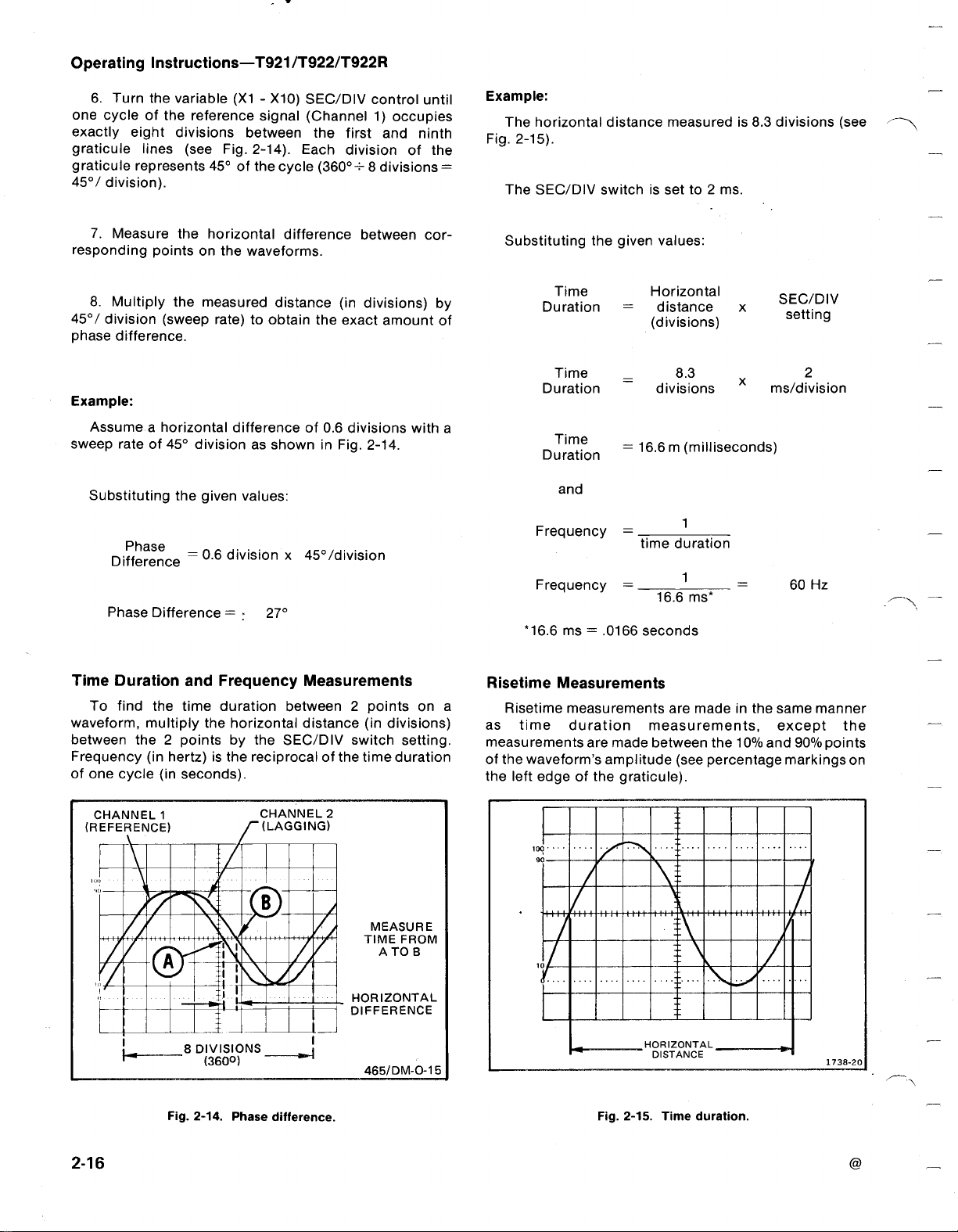
1=
Operating
6.Turn
one
exactly
graticule
graticule
45°/
7
.
responding
8.Multiply
45°/
phase
Example
Assumeahorizontal
sweep
Substituting
Instructions-T921/T922/T922R
the
variable
cycle of the reference
eight
divisions
lines
represents
division)
Measure
division
difference
:
rate of
.
the
points
the
(sweep
45°
the given
(X1-X10)
signal
between
(see
Fig.2-14).Each
45°ofthe
horizontal difference
on
the
measured
rate)toobtain
.
division
cycle
waveforms
distance
differenceof0.6divisions
as
shown
values
:
SEC/DIV
(Channel1)occupies
the
(3600-8divisions
.
the exact
in
control
first
divisionofthe
between
(in
divisions)
Fig.2-14
and
amount
with
.
until
ninth
cor-
by
of
=
a
Example
The
horizontal
Fig.2-15)
SEC/DIV
The
Substituting
:
.
Time
Duration
Time
Duration
Time
Duration
and
distance
switchisset
the given values
measuredis8.3divisions
to2ms
:
Horizontal
=
distance x
(divisions)
__
=16.6m(milliseconds)
8
.3
divisions
(see
.
SEC/DIV
setting
2
ms/division
Difference
Phase
Time
Duration
To
find
waveform,
between
Frequency
of
one
cycle
CHANNEL1
(REFERENCE)
Phase
the 2
=
0
.6
Difference=-270
and
Frequency
the time
multiply
(in
hertz)isthe
(in
duration
the
points
seconds)
division
horizontal
by the
x45°/division
between
SEC/DIV
reciprocalofthe
.
CHANNEL2
/-(LAGGING)
Measurements
2
points
distance
(in
switch
time
MEASURE
TIME
HORIZONTAL
DIFFERENCE
on
divisions)
setting
duration
FROM
ATOB
a
.
Frequency
Frequency=
'16
.6ms=
Risetime
Risetime
as
time
measurements
of
the
waveform's
the
left
edgeofthe
.
.
,0
0
90
=
.0166
Measurements
measurements
duration
are
made
amplitude
graticule)
1
time
duration
16.6ms'
seconds
are
madeinthe
measurements,
between
(see
.
the
percentage
10%and
momWOMMIN
mom
11r
:~
60 Hz
same
except
90%points
markings
i
manner
the
on
2-16
DIVISIONS
8
(3600)
Fig
.
2-14.Phase
difference
465/DM-O-15
.
HORIZONTAL
DISTANCE
Fig.2-15.Time
duration
1738-20
.
Page 30

Use
the following
1.Adjust
display
amplitude
2.Adjust
display
display
16)
bottom
top
just
.
3.Measure
between
to
the
pointB,Fig.2-16)
4.Use
the following
Risetime
Examples
on
setting of
The
the
:
horizontal
waveform
1 /is
the
the
10%
.
vertical
just
touches
the
and
=
distance
procedure
VOLTS/DIV
of
exactly5divisions
and
POSITION
touches
the0%graticule
the
100%
horizontal
90%
pointsonthe
.
formula
horizontal
distance
(divisions)
between
is5divisions
to
measure
VAR
controls
.
control
graticule
line
distance
waveform
to find
risetime
the
SEC/DIV
setting
10%
x
withaSEC/DIV
risetime
so
line
(see Fig.2-
(divisions)
and
90%
that
and
(point
:
switch
:
for
point
the
the
Operating
T922R
Instructions-T921/T922/T922R
RACKMOUNTING
Introduction
a
mount
The
Tektronix
inastandard
accordance
instrument
characteristics
Instrument
A
dimensional
of
the
T922R
A
manual
Rack
.
Dimensions
Height.A
to
mount
this
Width.When
the
minimum
right
front
railsofthe
allows
out
room
trackstooperate
move
smoothly
T922R
Oscilloscope
19-inch
with
the
following
will
meet
all
electrical
giveninSection1of
Dimensions
drawing
shown
is
least
5.25
instrument
used
width
showing
in
inches
inarack
with
the
of the
openingbetween
rack
oneach
sideofthe
freely,
in
and
outofthe
is
designed
rack.When
mounting
and
this
the
mounted
procedure,
environmental
manual
major
dimensions
.
Fig.1-2inSection1of
vertical
of
spaceisrequired
.
optional
slide-out
mustbe175/8
instrument
permitting
rack
the
.
tracks,
the
left
inches.This
for
the
instrument
to
in
the
this
and
slide-
to
Substituting
Risetime=5
Risetime
SIGNAL
AMPLITUD
the
given
values
:
cabinet
circulation,
Depth.Total
divisionsx1
=
5,us
/is/division
mounting
access
to rear
Slide-Out
The
optional
extended
without
the
cord
this
.
loo
I
1
.
}
E
.---_
i
ASURE
-
ME
+
E
FROM
TI
TO
B
the
Illustrationsatthe
slide-out
T922R
and
purpose
The
left
removing
slide-out
sideofthe
assembly
and
the
chassissectionisattachedtothe
intermediate
HORIZONTAL
DISTANCE
Fig.2-16.Risetime
chassis
of the
the
465/DM-0-13
be
the
rack,
.
assemblies
sections
rack.The
tracks
separated
positionofthe
the
depth
necessary
rack
is
18
inches
power
cord
clearance
hardware.(Additional
panel
connections
Tracks
slide-out
outofthe
in
the
any
interconnecting
the
extended
tracks
rack
for
instrumentfrom
.
tracks
consistoftwo
instrument
end
of this
track
assemblies.The
attachestothe
section
and
front
slides
allowsthe
stationary
are
packaged
.Toidentify
as
the
automatic
automatic
latch
.
to
This
.
maintenance
position,
cables are
and
section
stationary
and
between
T922R
and
intermediate
matched
leftorright
latch.When
should
mount
allows
and
room
is
required
permit the
the
be sure
assemblies-one
one
show
rear
the
tobeextended
sets
be
at the
T922R
the
room
the
may
beneeded
.)
T922R
or calibration
rack.To
long
enough
for
the
the
sectionofeach
rails
of
instrument.The
stationary
sections
andshould
assembly,
mounted
topofboth
for
necessary
to
operate
the
power
right
side
complete
the
rack,
note
in
in
and
out
not
the
a
air
if
be
for
for
.
of
2-17
Page 31

Operating
The
hardware
showninthe
the
hardware
compatible
methods,
Use
method
Mounting
Refertothe
recommended
only
not
the
used
Instructions-T921/T922/T922R
neededtomount
illustrations
supplied
withavarietyofcabinet
allofit
hardware
.
Procedure
illustrationsatthe
mounting
at
the
is
intendedtomake
will
be needed
thatisrequired
procedures
the
endofthis
racks
for
endofthis
.
slide-out
section.Since
the tracks
and
installation
this
installation
for
the
section
tracks
mounting
is
for
.
Removing
After
tracks,
further
Slide-Out
The
The
special
nent
smoothly
paraffin
operation
or
inital
the
T922R
adjustments
Track
slide-out tracks
finishonthe
lubrication.However,
even
rubbed
.
Installing
installation
can
be
under
Lubrication
normally
sliding
after
proper
the
onto
Instrument
the
and
adjustmentofthe
removed
normal
sliding
conditions
require
surfaces
tracks
if
the
adjustment, a
surfaces
or
installed
provides
slide-out
.
lubrication
no
do
not
thin
coating
may
without
.
perma-
slide
of
improve
Page 32

Operating
Instructions-T921/T922/T922R
FRONT
RAIL
MOUNTING
DEEP
RACK
Fig.2-17.T922R
MOUNTING
rackmounting
methods
RACK
SHALLOW
.
MOUNTING
1982-5D
2-19
Page 33

Page 34

Section
3-T921/T922/T922R
This
procedure
intended
for
LIMITS
Tolerances
do
not
include
in
this
check
called
specifications
1.Amplitude
out as
Description
allows the
in
incoming
use
given
equipment
test
instrument
are
performance
section
Calibrator
PERFORMANCE
basic
performance
inspectiontodetermine
are
for
.
TOLERANCES
instrument
the
error.Limits
specifications
requirements
Minimum
Amplitude
0.5%;signal
to10V;output
square
accuracy,
wave
amplitude,
.
under
and
onlyifthey
Specifications
signal,1kHz
AND
specificationstobe
acceptability
test
and
tolerances
are
in
the
TABLE
Test
within
10
Equipment
Vertical
mV
X
3-1
checked
newly
of
TEST
You
will
equivalent,
T921, T922,
the
the
equipment
results
.
Usage
Gain
gain
check
CHECK
without
purchasedorrecently
need
performacomplete
to
checks,
.
removing
EQUIPMENT
the
test
equipment
and
T922R.The
are the
minimum
.
a
tion
b
.
Calibration Fixture
theinstrument
calibrated
REQUIRED
listed
Performance
Specifications
necessary
Examples
Test
Tektronix
Generator
Tektronix
covers.It
instruments
Table
in
Check
given
accurate
for
of
Applicable
Equipment
PG
506
Calibra-
.'
067-0502-01
.
3-1,
is
.
or
of
for
2.Sine-Wave
Time-Mark
3
.
4.Termination
5.Cable
'RequiresaTM500
REV.B,
DEC
(3)
.
Generator
Generator
Series
1976
Frequency
MHz;output
15
variable
output
reference frequency,
amplitude
within0.3%
frequency
changes
Marker
marker
trigger
time coincident
Impedance,
connectors
Impedance
connectors
Power
from0.5to5Vp-p
impedance,
accuracy,
as output
.
outputs,
accuracy
output1msto0
Module
.
50
kHztoabove
amplitude
50
0
;
kHz
50
constant
reference
of
frequency
20 nsto0.5s;Timing
within
0.5%
.1
markers
with
f2;BNC
50
.
50i2;
BNC
.
Vertical
width
check.Triggering
;
Z
axis
;
;
has,
.
Signal
Signal
Amplifier
checks,Xbandwidth
input
checks
termination
interconnection
check
.
band-
checks
.
.
.
a.Tektronix
Sine-Wave
.
b.Tektronix
Tektronix
.
Tektronix
.
Amplitude
tant
Generator
a
MarkerGenerator
b.Tektronix
Generator
a
a.Tektronix
SG
Generator
Type
.
TG
2901
.
Part
Part
Leveled
503
.'
Cons-
191
Signal
Time-
501
.'
Time-Mark
011-0049-01
012-0057-01
.
.
Page 35

Performance
Description
6.Dual
7.T
Connector
8.Adapter
9.TV
Source
Use
the
basic
operating
mance
T922,
channel
Check.This
and
.
For
the
procedures
Check-T921
Input
Coupler
PRELIMINARY
following
mode
procedureisthe
T922R
except
T921,
use
the
.
/T922/T922R
Minimum
Connectors,
2
BNC
Connectors,
BNC
femaletoBNC
Composite
least
100
video,
outputatleast
PROCEDURE
stepstoput
before
that
NOTE
channel1control
your
proceeding
the
T921
male
mV
same
has
Specifications
BNC
female
.
BNC
.
female
Sync,
output
(or
Composite
instrument
with
the
for
the T921,
only
one
settings
Table
to
.
at
230
mV)
into
a
Perfor-
vertical
and
3-1
Signal
Signal
Signal
TV
.
(cont)
interconnection
Interconnection
Interconnection
SYNC
3.Set
Usage
.
.
.
Trigger
Vertical
POSITION
VOLTS/DIV
VAR
CH1AC-GND-DC
.
the
controlsasfollows
Vertical
Mode
(both)
(both)'2
(both)
Examples
Test
a.Tektronix
a.Tektronix
a.Tektronix
a.Any
specified
TV
video
set
.
:
Amplifier
1
CH
Midrange
mV
Detent
DC
output,
of
Equipment
Part
.
Part
Part
source
(cw)
Applicable
067-0525-00
103-0030-00
103-0028-00
with
the
including
.
.
.
a
1
.
Check
that
the
and
the
HI-LO
Range
cabinet
voltage.In
Selector
Range
In
normally
normally
should
a
set,
turn
appropriate
MODE
(T921
and
T922)
the United
switchisnormally
Selector
Europe,
change
different
2
.If
the 120
connect
the
to
Allow
Performance
must
have
of
+25°Cwithin5°Ctoensure
procedure
switchisnormally
the
Power
set for
set forLO.
instrument
a
the
voltage
the
power
AUTO,
20
been
will
240Vand
Power
range
V/240Vand
power
source
and
minute
Check
adjusted
meet
Power
Input
Voltage
Selector switchonthe
are set
States,
Input
Only
cord
on,
SOURCE
specificationsinSection1.
the
set
for
set forHIatthefactory
Voltage
the
HI-LO
qualified
Input
Voltage
setting
.
HI/LO
plugtothe
connect
and
turniton.Set
to
NOTE
warmup
Procedure.This
before
atanambient
Selector
bottom
for
your
Power
switches
test
INT
that
Input
120Vand
Selector switch
Range
service
Selector
power
equipment
.
starting
instrument
temperature
checksinthis
power
Voltage
the
Selector
personnel
Switch
are
properly
source
the
switch
of
the
input
HI-LO
is
is
to
and
to
an
trigger
the
.
4.The
trace
TY,
FOCUS,
defined
'Unless otherwise
VOLTS/DIV
procedure
CH2AC-GND-DC
Time
SEC/DIV
X1-X10
SOURCE
MODE
POSITION
SLOPE
LEVEL
shouldbevisibleonthe
trace
.
(variable)X1
POWER
settings
and
.
ON
ASTIG
stated,
light
controls
use
throughout
GND
Base
.5
ms
(unmagnified-
fully
ccw)
INT
AUTO
Midrange
+OUT
Midrange
should
beon
graticule.Adjust
for
low
the
1X
PROBE
the
Performance
aridabaseline
INTENSI-
intensity,
window
well-
for
Check
3-2
REV.B
APR
1977
Page 36

Performance
Check-T921/T922/T922R
Baseline
lines.If
side
panel (T921
tal
graticule
This
not,
ends
should
adjust
and
lines
the
be
parallel
R472,
TR
T922)
.
preliminary
PERFORMANCECHECK
1.CH1and
a.Connect
appropriate
display
to
within
b.CHECK-Deflection
Table
CH2Deflection
test
equipment
POSITION
the
graticule
3-2
within3%(+20°C
controlasneeded
with
ROT,
until
trace
procedure
as
area)
accuracy
to
horizontal
(trace
aligns
.
graticule
rotation)
with
PROCEDURE
Accuracy
showninFig.3-1
to
center
.
forCH1
+30°C)
according
.
in left
horizon-
(use
the
VOLTS/DIV
(1X
PROBE
WINDOW)
2
mV
5
mV
10
mV
20
mV
.2V
2V
c.Set
:
TABLE
Deflection
Amplitude
Calibrator
Output
10
mV
mV
20
50
mV
.1
V
1
V
10V
AC-GND-DC
CH
1
CH2AC-GND-DC
Vertical
CH
Mode
2POSITION
3-2
Accuracy
Vertical
Deflection
(divisions)
'
5
4
5
5
5
5
±3%
Tolerance
(divisions)
4
.85to5
3
.88to4
4.85to5.1
4
.85to5
4
.85to5
4
.85to5
GND
DC
CH
2
As
needed
.15
.12
5
.15
.15
.15
AMPLITUDE
CALIBRATOR
BNC
T-CONNECTOR
4
1
"0
OSCILLOSCOPE
NOMMMENE
HEMENEENOM
NUMENE
Mono
Ma
ON
:
:nWMMJ
00
mlim
DUAL-INPUT
CONNECTOR
1982-02
REV.A,
JUNE
1976
Fig.3-1.Deflection
accuracy
andXgain
check
test
setup
.
3-3
Page 37

Performance
Check-T921
d.CHECK-Deflection
to
Table
3-2
within3%(+20°Cto+30°C)
e
.
Amplitude
Set
2
.
1
and
CH
a.Set
CH
CH1and
b.CHECK-Display
to
less
turned
c.Set
fully
counterclockwise
:
d.CHECK-Display
divisions
turned
to
less
fully
counterclockwise
/T922/T922R
Accuracy
Calibratorto0.1volt
2
VAR
(Variable)
CH2VOLTS/DIV
amplitude
than 2
divisions
.
Vertical
Mode
CH1AC-GND-DC
CH2AC-GND-DC
amplitude
than2divisions
.
forCH2
Volts/Div
to20mV
reducdivisions
with
CH
reduces
with
CH1VAR
.
.
es
2
VAR
CH
DC
GND
according
Range
.
from
control
1
from
control
5
5
For
bench
3
and4and
3.Rear
a.Set
Connect
b
.
c.Set
amplitude
versionsofthe
proceed
Vertical
:
SEC/DIV
VOLTS/DIV
CH1and
FRONT-REARREAR
Vertical
Trigger
test
amplitude
output
.
NOTE
with
Inputs
Mode
Mode
equipment
calibrator
T921
step 5
(T922R)
CH
2
as
and
.
shown
for
a 0.5volt
T922,
.2
m
.1
CH
AUTO
1
in
skip
Figure
standard
steps
3-2
.
e.Return both
Reduce
INTENSITY
f.Disconnect
VAR
setting
Test
equipment
STANDARD
AMPLITUDE
CALIBRATION
GENERATOR
controls
foradim
.
to
detent
display
position
.
.
d.CHECK-Display
divisions
e.Set
.
CH1FRONT-REAR
REAR
amplitude
CH
1REARCH
DUAL-INPUT
COUPLER
to
FRONT
2
is4.85
.
to5.15
1982-51
3-
Fig.3-2.T922R
4
rear
input
test
setup
.
REV.B,
DEC.1976
Page 38

CHECK-No
f
.
g.Set
Vertical
h.CHECK-Display
divisions
.
i.Set
CH2FRONT-REAR
j.CHECK-No
4.Rear
EXT
a.Disconnect
connectitto
b.Set
:
c.Set
Amplitude
vertical
Mode
vertical
TRIG
BNC
rear-panel
EXT
X
FRONT-REAR
Trigger
deflection
to
CH2.
amplitude
deflection
orXInput
cable
from
EXT
TRIG
TRIG
or
SOURCE
calibrator
.
is4.85
to
FRONT
.
.
(T922R)
dual
input
orX
input
REAR
X-Y
Amplitudeto5
coupler
(see
volts
to5.15
and
Fig.3-2)
.
6.5divisions
start
.
adjust
Performance
c.CHECK-Horizontal
(set
horizontal
andendofdisplay)
d.Disconnect
e.Set
6
.
SOURCE
CH1Bandwidth
a.Connect
b.Set
:
test
VOLTS/DIV
AC-GND-DC
LEVEL
c.Set
generator
output
amplitude
Check-T921/T922/T922R
deflectionisbetween3.5
POSITION
.
test
equipment
INT
.
to
equipment
frequencyto50
for5division
.
as
shown
(both)
(both)
as
neededtoview
in
Fig.3-3
kHz
(reference)
display
2
mV
DC
Fully
.
and
.
cw
and
d.CHECK-Display
about5divisions
by
Do
notallow a
crt.This
e.Set
can
EXT
f.CHECK-No
g.Disconnect
X
Gain
5
.
a.Set
:CH1AC-GND-DC
.
bright
burn
TRIG
orXFRONT-REAR
horizontal
test
SOURCE
INTENSITY
is
two
dots
spottoremain
the
crt
phosphor
deflection
equipment
separated
stationaryonthe
.
to
.
.
GND
X-Y
Foradim
horizontally
FRONT
.
display
d.Set
e
7.CH
a.Set
b.Move
cable
CH2input
C
adjust
d.Set
generator
.
CHECK-Display
2Bandwidth
:
the
and50i2
connector
.
Set
generator
output
generator
e.CHECK-Display
frequency
(T922
Vertical
sine-wave
termination)
.
frequencyto50
amplitude
frequencyto15
to15MHz
amplitudeisat
and
T922R
Mode
generator
from
output (through500
CH1input
for5division
amplitudeisat
.
least3.5
CH
kHz
(reference)
display
MHz
.
least3.5
divisions
Only)
2
connectorto
.
divisions
.
and
.
'
b.Connect
calibration
REV.B,
DEC.1976
test
generator
equipmentasshowninFig.3-1
output
amplitudeto5V.
and
set
f
and
.
Disconnect
reduce
generator
INTENSITY
from
setting
CH2input
foradim
connector
display
.
3-
5
Page 39

Performance
Check-T921
/T922/T922R
8.X
Bandwidth
a.SET
b.Connect
and500
c.Set
adjust
output
horizontal
d.Set
:
SEC/DIV
SOURCE
INTENSITY
X1-X10
sine-wavegenerator
terminationtoX
generator
frequencyto50
amplitude
deflection
generator
.
frequencyto1
1
X-Y
For
X10
through50O
(EXT)
input
.
kHz
for10divisions
MHz
Fig.3-3.Bandwidth
ms
visible
display
cable
(reference)
(about1volt)
.
and
of
check
test
f.Disconnect
g.Set
When
control
instructed
9.Low
a.Set
setup
.
SOURCE
making
as
needed
otherwise
Frequency
:
test
equipment
to
INT
.
.
NOTE
trigger
checks,
forastable
adjust
display,
.
Triggering
SEC/DIV
X1-X10
Vertical
(variable)X1
Mode
10
CH
MODE NORM
the
ms
(fully
1
LEVEL
unless
ccw)
e.CHECK-Display
3-6
amplitudeisat
least7divisions
.
b.Connect
10X
probetoCH1input
.
REV.A,
JUNE
1976
Page 40

c.Lay
CH1VOLTS/DIV
display
d.CHECK-Stable
+OUT
NORM
e.Remove
f
SOURCE
10.1
a.Connect
b.Set
.
Return
.
and
modes
MHz
probe
-IN
INT
to
Internal
:
near
ac-line-voltage
switch
and
display
positionsofSLOPE
in
LINE
and
probe
.
VAR
to
detent;MODE
.
Triggering
test
equipment
CH1VOLTS/DIV
SEC/DIV
INT
VAR
as
control
can
source
shown
source
be
switch
1
.5
and
for0.4
obtainedinboth
for
AUTO
positions
NORM;and
to
in
Fig.3-4
V
Ns
adjust
division
and
.
.
c.Set
adjust
d.CHECK-Stable
+OUT
and
11.1
a.Set
100
c
d.CHECK-Stable
+OUT
and
sine-wave
output
and
NORM
MHz
:
b.Adjust
mV
(one
.
Set
:
and
NORM
-IN
-IN
Performance
amplitude
positions
.
External
CH1VOLTS/DIV
sine-wave generator
divoncrt)
SOURCE
positionsofSLOPE
.
Check-T921/T922/T922R
generator
for0.5
display
of
Triggering
.
display
frequency
division
can
be
SLOPE
switch
output
canbeobtained
switch
for1MHz
display
obtained
for
.1
V
amplitude
EXT
for
.
both
both
on
in
AUTO
AUTO
and
both
for
both
SINE-WAVE
GENERATOR
50
TERMINATION
BNC
FEMALE
BNC
TO
FEMALEADAPTER
T-CONNECTOR
S2
It
I
_ilea,
III
OSCILLOSCOPE
sofflawwwamn
SEENEREMNO
am
MMOMMOM
soon
M
HEMEMENE
E "
%
11~
!
REV.B,
DEC
.
1976
Fig.3-4.Triggering
and
Z-axis
50
CABLES
input
S2
check
test
setup
1982-04
.
3-7
Page 41

Performance
12
.
15
MHz
.
Set
b.Set
output
VOLTS/DIV
+OUT
and
13.15
amplitude
c
.
CHECK-Stable
and
NORM
MHz
a.Set
Check-T921/T922/T922R
Internal
:
sine-wavegenerator
to.1V
-IN
positionsofSLOPE
modes
External
:
SOURCE
Tra
iggering
SOURCE
CH1VOLTS/DIV
SEC/DIV
for
a 3
division
.
display
.
Triggering
INT
50
.2
frequency
display;then
can
be
switch
EXT
mV
/is
to 15
obtained
for
both
MHz
and
setCH1
in
both
AUTO
14.Z-Axis
a.Set
b.Set
adjust
c.Disconnect
trigger)
rear of
CHECK-Trace
d
.
intensity.(Adjust
stable
e.Disconnect
Input
:
sine-wave generator
output
display
amplitude
input
and
instrument
.)
CH1VOLTS/DIV
SEC/DIV
SOURCE
MODE
for5division
S2
cable
50
connectitto
.
modulationisnoticeableatnormal
LEVEL
test
setup
fromXor
controlasrequiredtoobtain
.
1
V
.1
ms
INT
AUTO
frequencyto50
display
EXT
EXTZAXIS
kHz
.
(external
connector
and
at
b.CHECK-Stable
+OUT
and
-IN
and
NORM
positionsofSLOPE
.
TIME
MARK
GENERATOR
display
can
be
obtainedinboth
switch
for
both
AUTO
TERMINATION
50
15
.
a.Connect
SZ
Sweep
Rate
Accuracy
test
setupasshown
OSCILLOSCOPE
SEHIMENINE
MM
MENNEN
1
sing
Fig.3-5
in
-------------
.
3-8
50
S2
CABLE
Fig.3-5.Timing
accuracy
check
test
setup
1982-05
.
REV.C
JUL
1977
Page 42

Set
:
b
.
c.CHECK-SEC/DIV
3:Oneortwo
over center 8
a
temperature
time
divisions.Accuracy
Normal
SEC/DIV
switch
setting
.2
/is
.5
/is
1
Ps
2
/is
5
us
_
10
/is
20 ps 10
50
Ps
.1
ms
.2
ms
.5
ms
1
ms
2
ms
5
ms
10
ms
20ms
50
ms
.1
s 0.1s
._2
s 0.1second
_
5 s 0.5second
CH1VOLTS/DIV
SOURCE
MODE NORM
accuracy according
marks,asindicated,
specifications
.
range
of
TABLE
Sweep
+20°C
to
3-3
Timing
+30°C
Accuracy
Time-mark
generator
output
0.1microsecond
0.5mi
crosecond
1
microsecond
1
microsecond
5
microsecond
10
microsecond
microsecond
50
microsecond
millisecond
0
.1
0.1millisecond
0.5millisecond
1
millisecond
1
millisecond
5
millisecond
10
millisecond
10
millisecond
50
millisecond
econd
V
.2
INT
Table
to
within3%(0
.24
apply
.
crt
display
(marker/division)
2
1
1
2
1
1
2
1
1
2
1
1
2
1
1
2
1
1
2
1
3-
div)
for
_
Table
(0 .4
after
setting
anything
specifications
+30°C.
SEC/DIV
17.Rear
_
Performance
c.CHECK-Magnified
3-4:Oneortwo
div)
over center 8
the
startofthe
(one
division
beyond
the
apply
d.Return
e.Disconnect
X1-X10toX1
test
Magnified
switch
setting
.2
/is
.5
ps
1
ps
.5
ms
a.Set
Panel
:
generator
10
50
.1
50
Outputs
Vertical
CH1VOLTS/DIV
SEC/DIV
Trigger
Trigger
Check-T921/T922/T922R
sweep
time
accuracy
marks,asindicated,
divisions.Exclude
sweep;2.5divisions
for0.5
100th
,us
and1/is
magnified
divisions.Accuracy
foratemperature
and
SOURCE
equipment
TABLE
Sweep
3-4
Timing
.
Accuracy
Time-mark
output
(markers
nanosecond
nanosecond
microsecond
microsecond
(T922R)
Mode
MODE
SOURCE
according
within
the
first
for
the0.2
settings)
rangeof+20'C
INT
.
to
crt
display
/division)
2
1
1
1
CH
1
.1
.5
ps
AUTO
INT
to
5%
50 ns
ps
and
to
16.Magnified
a.Set
b.Set
VOLTS/DIV
If
you
time-mark
(external
:
time-mark
as
cannot
generator
trigger)
Sweep
necessary
500termination.Set
LEVEL
REV
A,
.
control
DEC.1976
Accuracy
X1-X10
SEC/DIV
generator
obtain
a
trigger
connector
forastable
to
foravisible
NOTE
stable
display,
outputtotheXor
via
MODE
to
display
(fully
X10
ps
0
.2
10 ns
(adjust
display)
.
connect
a 500cable
and
EXT
.
cw)
CH
the
EXT
and
adjust
Connect
b
.
connector.Connect50O
Connect
.c.
50f2terminationtoCH
CHECK-Display
1
Disconnect
d
.
tor
and
connectitto
e.CHECK-Display
(see
Fig.3-7)
f.Disconnect
50f2BNC
cable
.
cable
cable
termination
tilted
is
from
SWEEP
is
and
SWEEP
to
vertical
1
line
(see
SWEEP
leading
GATE
RAMP
OUT
edge
termination
to free
Fig.3-6)
of
.
RAMP
endofcable
input
.
.
connec-
OUT
connector
squarewave
OUT
.
3-
.
9
Page 43

Performance
Check-T921/T922/T922R
Fig.3-6.SWEEP
RAMP
OUT
display
c
.
Set
generator
d.Adjust
e.Set
:SINGLE
Input
f
.
CHECK-No
g.Push
RESET
h.CHECK-READY
.
i .
Set
CH1Input
j.CHECK-Crt
extinguishes
.
LEVEL
for0.1
second
forastable
SWEEP
Coupling
visible
and
display
release
lamp
CouplingtoDC
is
swept
only
display
SINGLE
GND
.
.
lights
once
time
.
.
marks
.
and
SWEEP
READY
.
(in)
lamp
18.Single
a
.
Connect
50S2BNC
Fig.3-7.SWEEP
Sweep
(T922R)
time-mark
cable
and50S2
GATE
OUT
display
.
generatortofrontCH2
BNC
termination
.
input
via
k.Disconnect
19.TV
We
recommend
you
Trigger
are
willdofor
The
amplitude
check
You
can
VOL
TS/DIV
composite
a.Connect
b.Set
test
equipment
NOTE
that
you
only
goingtobe
the
using
check-such
it.Any
NOTE
both
settings
the
check
INT
just
giveninthis
and
EXT
the
INT
settingtoattenuatethe
syncor2.3divofcomposite
test
setup
as
showninFig.3-8
:
SEC/DIV
CH
1
VOLTS/DIV
.
check
asaTV
trigger
trigger
theTVtrigger
TV
signal
source
set
.
procedure
are
requirements
by
using the
signalto1
video
.
.1
ms
.1
V
if
to
.
divof
.
b.Set:CH1VOLTS/DIV
SINGLE
SEC/DIV
0
3-
1
SWEEP
.1
REPETITIVE
20
ms
(out)
c.Set
(or
about2.3
MODE
signal
source
for1division of
divisionsofcomposite
TV
composite
video)
REV.A,
sync
.
DEC.1976
Page 44

(^
100
230
TV
SOURCE
SET
mVCOMP
mV
FOR
COMP
SYNC
VIDEO)
INPUT
DUAL
CONNECTOR
Performance
OSCILLOSCOPE
I
MRSOMMEMEM
EMBEEMEMME
I
LLLM
S9011
M,o
Check-T921/T922/T922R
n
O
d.Adjust
display
on
on
.
e
.CHECK-Stable
TV
field)
f.Set
g
.CHECK-Stable
TV
line)
1982-0s
Fig.3-8.TV
LEVEL
.
:
.
and
displayispresent
SEC/DIV
displayispresent
SLOPE
as
needed
(display
50
/is
(display
to
trigger
trigger
triggers
triggers
check
j .
on
TV
k
.Set
I . .
on
TV
m
.Disconnect
test
setup
.
CHECK-Stable
line)
.
:
CHECK-Stable
field)
.
displayispresent
SEC/DIV
displayispresent
test
setup
(display triggers
.1
ms
(display triggers
.
h.Set
i .
Adjust
display
:
.
LEVEL
SOURCE
and
SLOPE
as
EXT
needed
to
trigger
END
PROCEDURE
OF
3- 1
1
Page 45

Page 46

WARNING
THE
FORUSE
AVOID
SERVICING
OPERATING
QUALIFIED
FOLLOWING
PERSONAL
SERVICING
QUALIFIED
BY
OTHER
INSTRUCTIONS
TO
DO
INJURY,
THAN
SO
.
INSTRUCTIONS
PERSONNEL
DONOT
THAT
UNLESS
ONLY
PERFORM
CONTAINED
YOU
ARE
.TO
ANY
IN
ARE
Page 47

Page 48

SERVICING
USE
BY
SHOCK,
VICING
INFORMATION
QUALIFIED
DO
NOTREMOVE
UNLESS
ADJUSTMENTS
SERVICE
QUALIFIED
WARNING
IN
THE
FOLLOWING
PERSONNEL
INSTRUMENT
TO
DO
SO
.
ONLY
COVERS
SECTIONS
.
OR
Section
INTENDED
IS
TOAVOID
PERFORM
4-T921/T922/T922R
FOR
ELECTRIC
ANY
SER-
When
done
Adjustment
corrected
before
LIMITS
Limits
onlyifthey are
the
oscilloscope
error
and
Specification
.
ADJUSTMENT
Some
identified
adjustments
withanINTERACTION
PARTIAL
You
can
perform
replacing
between
components
major
IMPORTANT-PLEASE
properly,
Procedureisnot
tolerances
called
under
this
procedure
intended as a
continuing.Refertothe Service
AND
section.Tolerances
test
TOLERANCES
are instrument
outasperformance
anddonot
include
INTERACTION
interact
with
step
PROCEDURES
partofthe
or
re-adjustments.Do
just
adjustment
to
touch
not
READ
allows
youtoadjust
troubleshooting
specifications
requirements
given
are
test
equipment
others.These
.
procedure
the
up
performance
change
the
BEFORE
Information
in
for
the
are
after
setting
USING
the
instrumenttoits
guide.Any
section
of
the-8V
instrument
To
adjust
accordingtothe nearest
use
the
test
or the
setupina
re-adjustmentofother
adjustment
met.Ifitis
any
steps
TEST
The
test
required
Specifications
necessary
THIS
original
trouble
for
listed in
you
further
supply
.
only
partofthe
setup
giveninthe step
preceding
onlyifthe tolerance given
necessarytoreset
EQUIPMENT
equipment
for
complete
given
for
accurate
PROCEDURE
performance
find
during the
information
unless
you
preceding
step.To
partsofthe
the
INTERACTION--
listedinTable
calibrationofthe
for
the
equipment
calibration
specifications.The
procedure
.
intendtore-adjust
instrument,
an
adjustment,
set
Control
you
intend
prevent
instrument,
for
that
partofthe
the
Settings
unnecessary
REQUIRED
4-1,orequivalent
oscilloscope
are the
.
should
entire
the
controls
and
perform
to
an
reset
stepisnot
also
check
step
minimum
be
.
is
.
Description
1.Digital
2.Time-Mark
3.Amplitude
'Requires
REV.A,
TM500
JUNE
Voltmeter
Generator
Calibrator
Series
1976
Minimum
Range,0to9Vdc
accuracy
Markers,0.5
accuracy,
Signal
to50V
frequency,1kHz;amplitude
accuracy,
Power
Module
within0.3%
/isto0.5s
within0.3%
amplitude, 10
square
within0.3%
.
TABLE
Test
Specifications
;
.
;
.
mV
wave
;
.
4-1
Equipment
Power
Y-axis
etry
adjustment,
and
timing
Vertical
Usage
supply
alignment,
adjustment.a.Tektronix
geom-
sweep
adjustments
gain
adjustment.a.Tektronix
.
Examples
Test
Digital
a.Tektronix
Time-Mark
b
Generator
Calibration
Multimeter
Tektronix
.
of
Equipment
DM
TG
Generator
2901
.
PG
Generator
Applicable
501
.'
501
.'
Time-Mark
506
.'
Page 49

Adjustments-T921
Description
4.Square-Wave
5.Cable
6.Termination
7.Low-Capacitance
Screwdriver
8.Screwdriver
9.Alignment
10.10X
11
.
Probe,
Tool
Attenuator
1OX
/T922/T922R
Generator
'
TABLE
Minimum
Frequency,1kHz
100
kHz;risetime,
or
less
Length, 42in. ;
50
iZ;connectors,
Impedance,
BNC
.
Length,3in.shaft;bit
3/32in.
Ratio,
1OX
50
G;connectors,
Attenuation,
be
compensated
characteristicsofT921/T922/
T
922R.
.
;
Specifications
and
2 ns
impendance,
BNC
i'2
50
;
connectors,
impedance,
BNC
10X;Probe
for
input
.
size,
.
can
4-1 (cont)
Usage
High
frequency
sation
and
attenuator
Signal
Signal
Variable
ments
Variable
ments
Vertical
high-frequency
sation
Vertical
ments
Vertical
pensation
adjustments
interconnection
termination
capacitor
.
resistor
.
attenuator
adjustment
attenuator
.
attenuator
.
compen-
vertical
adjust-
compen-
.
.
.
adjust-a.
and
.
adjust-a.
com-
Examples
a.Tektronix
Calibration
Tektronix
b
.
Wave
Generator
a.Tektronix
a.Tektronix
General
toolG.C
a.Xcelite
a.General
toolG.C.8722
Tektronix
a.P6006, Tektronix
010-0160-00.(Standard
accessory
Test
8722
.
R-3323
for
of
Applicable
Equipment
PG
506
Generator
Type
.
Part
012-0057-01
Part
011-0049-01
Cement
.
.
Cement
.
Part
011-0059-02
T921/T922
106
adjustment
Adjustment
Part
.'
Square-
.
.
.
.)
12.Adapter
'Requires
TM500
PRELIMINARY
Dangerous
your
instrument.To
touch
exposed
the
instrumentisoperated
Disconnect
voltage
instrument
1.Remove
the
(threeonthe top
halves
Because
T922R,
locationsonthe
source
T921/T922
apart
use
.
the cabinet
.
of
Fig:4-1
Probe-tip-to-BNC
Series
Power
Module
.
PROCEDURE
WARNING
potentials
power
while
cabinet,
and
the
T922R)inplaceofFigs.4-2
existatseveral points
prevent
connections
cord plug from
disassemblingorrepairing
three
different
from
remove
on
(which
electrical
or
components
with
the
the
instrument.To
the
six
the
bottom)
mechanical
shows
.
inside
shock,donot
cover
removed
power
retaining
and
slide
layoutofthe
the
adjustment
through
when
input
this
remove
screws
.
the
4-4
Vertical
compensation
attenuator
.
and
4-6.The
canberemoved
captive
captive
cabinet
loosen the
2.Check
and
fhe
tings.For
the
bottomofthe cabinet.For
the
internal
settingofthe
RefertoElectrical
3.Turn
warm-up
For
ambient
T922R
screws.To
screws
half
away
captive
the
High/Low
the
T921
locationsofS701
range
the instrumentonand
before
best
overall
temperature
a.Tektronix
cabinet
independently
remove
90
degrees
from
the instrument.Usealarge
screws
.
120
V/240
selector
and
T922,
selector
Parts
List
starting
the
accuracy,
of
+20°C
Part
013-0054-00
is
made
.
Each
a cabinet
counterclockwise
V
range
switch
both
the
and
switch,
for
allowatleast20minutes
adjustment
make
to
two
of
halfisheld
half,
selector
S705
for
switches
T922R,see
S705.If
correct
+30°C
are
you
change
fuse
procedure
adjustmentsinan
.
pieces
the
which
onby
turn
the
and
lift
coin
switch
S701
correct
located
Fig.4-1 for
change
line
fuse
values
.
.
.
six
six
the
to
set-
on
the
.
,
4-2
REV.A,
JUNE
1976
Page 50

84132
CH
DC
BAL
84232
DC
I
Adjustments-T921
CH
2
f
BAL
GAIN
84251
84334
-8V
8773
ADJ
/T922/T922R
1982-54
REV.B,
DEC.1976
Fig.4-1A
& B.T922R
adjustment
locations
.
4-
3
Page 51

Adjustments-T921
/T922/T922R
Equipment
1.Digital
2
.
Time-Mark
3.50S2BNC
1.Set
the
For
adjustment
control
INTENSITY
Vertical
Required
Voltmeter
Cable
Front
Do
not
settings
Mode
Generator
Panel
preset
of
the
and
procedures
A.DISPLAY
Controlsas
NOTE
internal
NOTE
T921,
use
.
midrange
CH
1
Follows
controls
the
:
.
channel
AND
1
POWER
4.500Termination
5.Screwdriver
6.Low-Capacitance
front
neededtomaintain
2.-8VPower
Do
unless
a.Connect
R775
between-7.96Vand
panel),
not
change
you
and
ground
SUPPLY
and
intendtore-adjust
digital
Screwdriver
ASTIG
Supply
control
a
well-defined display
NOTE
the
settingofthe-8V
voltmeter
(see
Fig.4-2).If
-8
.04V,proceed
(left
sideofcabinet)
the
entire
between
meter
.
adjustment
instrument
the-8V
does
to partb.
not
side
as
.
of
read
1
CH1VOLTS/DIV
VOLTS/DIV
AC-GND-DC
SEC/DIV
X1-X10
SOURCE
MODE
SLOPE
LEVEL
CH1POSITION
Horizontal
Set
all
other
should
above.Adjust
produce
2
VAR
(both)
(both)
POSITION
controlsasdesired.The
a
baseline
the
INTENSITY
V
detent
GND
.1
ms
X1
(fully
INT
AUTO
+OUT
midrange
midrange
midrange
trace
and
with
ccw)
the
FOCUS
oscilloscope
controls
controls
set
as
(on
b.ADJUST-R773,
dc
.
c.Disconnect
-8VAdj
digital
voltmeter
(see
.
Fig.4-2)
for-8
.00
V
'Unless
VOLTS/DIV
4-4
otherwise
settings
stated,
throughout
use
the
this
procedure
1X
probe
.
window
for
Fig.4-2
T922)
.
.
Power
supply
adjustment
location
(bottomofT921 and
REV.B
APR
1977
Page 52

3.Trace
a.Position
line
Rotation
trace
.
b.ADJUST-TRACE
center
horizontal
4.Y-Axis
a.Set
CH1AC-GND-DC
graticule
Alignment
b.Connect.1ms
1
inputvia500BNCcableand50
CH
1
c.SetCH
than
8
baseline
d.Set
and
rotate
center
VOLTS/DIV
divisionsofvertical
below
bottom
SEC/DIV
horizontal
graticule
line
verticallytocenter
ROT,
R472,toalign
line
.
toDC.
from
markers
and
time-mark
VARtoobtain
deflection
graticule
to
obtain
POSITION
line (off
about
to
.
horizontal
graticule
trace
generator
f2BNCtermination
slightly
and
position
screen)
one
marker/division
align
marker
a
display
.
with
more
with
to
ADJUST-Y-Axis,
e
.
marker
f.INTERACTION-Position
horizontal
with
horizontal
rotation
5.Geometry
a.Move
.
b.ADJUST-Geom,
alignmentsofmarkers
c.INTERACTION-Between
Repeat
with
vertical
d.Disconnect
with
.
Then
both
center
graticule
graticule
re-check
display
adjustment
graticule
time-mark
Adjustments-T921
R474,
(see
Fig.4-3)
vertical
line
graticule
and
line.If
Y-axis
display
check
alignment
baselinetobottom
R473,
with
the
(see
vertical
Geometry
lines
for
.
alignmentofmarkers
best
generator
/T922/T922R
toaligncenter
line
.
baselinetocenter
that
baseline
not,-re-adjust
.
graticule
Fig.4-3)
line
for
graticule
and
.
aligns
trace
.
best
lines
Y-axis
.
.
INTERFACE
CIRCUIT
BOARD
ASTIG
R477
GEOM
R473
TRACE
R472
ROT
GAIN
R126
t
TOP
FRONT
1982-35
REV.B,
DEC
.
1976
Fig.4-3
Interface
.
board
adjustment
locations
.
4-5
Page 53

Adjustments-T921
Equipment
1.Digital
2.Amplitude
3.Square-Wave
4.500BNC
5.50OBNC
6.Alignment
Required
Voltmeter
PRELIMINARY
Preset
front
INTENSITY
/T922/T922R
Calibrator
Generator
Termination
Cable
Tool
CONTROL
panel
controlsasfollows
Use
Channel1control
SETTINGS
midrange
B.VERTICAL
settings
:
AMPLIFIER
NOTE
and
procedures
7.Screwdriver
8.Low-Capacitance
9.10X
10.10XAttenuator
11.Probe-tip-to-BNC
The
the
controls
controlsasneeded
while
making
for
Probe
oscilloscope
setasabove.Adjust
adjustments
the
T921
.
Screwdriver
Adapter
should
produceabaseline
INTENSITY
to
maintainawell-defined display
.
and
trace
FOCUS
with
FOCUS
Vertical
VOLTS/DIV
AC-GND-DC
VAR
(both)
SEC/DIV
X1-X10
SOURCE
MODE
SLOPE
LEVEL
POSITION
Set
all
other
Mode
(both)'
(both)
(all)
controlsasdesired
midrange
CH
1
2
mV
GND
detent
.5
ms
X1
(fully
INT
AUTO
+OUT
midrange
midrange
1.Vertical
a.ADJUST--CH
trace
between2mV
b.SET:Vertical
c
.
ADJUST-CH
cw)
.
trace
between2mV
2.Vertical
You
gain unless
components
a.Set
to
CH1
Preamplifier
shift
while
shift
while
Output
shouldnot
VOLTS/DIV
.
1DCBAL,
switching
and10mV
Mode
2
DC
switching
and10mV
Amplifier
have
you
have
.
(both)to5
Balance
.
CH2.
BAL,
.
NOTE
to
re-adjust
replaced
R4132
CH
R4232
CH
mV/div
1
2
Gain
(see
Fig.4-4)
VOLTS/DIV
(see
Fig.4-4)
VOLTS/DIV
the
vertical
the
crtorother
and
output
Vertical
for
no
control
for
no
control
Mode
3
Unlessotherwisestated,usethe1X
VOLTS/DIV
4-
6
settings
throughout
this
procedure
probewindowfor
.
b.Set
Gain,
R126
(see
Fig.4-3)tophysical
REV.A,
midrange
JUNE
.
1976
Page 54

FRONT
Fig.4-4.Vertical
amplifier
adjustment
locations
(bottom
view
Adjustments-T921
T921
of
and T922)
/T922/T922R
1982-15
.
c.Connect
(see
Fig.4-4).Select
reading
with
has
toward
third
3.Vertical
(standard
unterminated
.
d.Set
vertical
center
e.Rotate
increased
topofscreen)
f.Adjust
graticule
g.Disconnect
a.Set
:VOLTS/DIV
b.Connect
digital
POSITION
horizontal
vertical
Gain,
Preamplifier
output)
POSITION
150
mV
R126
line
above
digital
AC-GND-DC
Vertical
a1kHz, 20
signal
cable
.
voltmeter
rangeonmeter
graticule
from
.
(see
voltmeter
Mode
between
controlsotraceisaligned
line.Note
control
readinginpartd(trace
Fig.4-3),sotrace
center
horizontal
.
Gain
(both)
(both)
mV
amplitude
to
CH
1
P4-9
and
foratleast
meter
until
meter
aligns
graticule
5
mV
DC
CH
1
calibrator
input
viaa50
P4-11
500
mV
reading
reading
moved
with
line
.
.
n
d.Move
and
e.ADJUST-Gain,
display
f.INTERACTION-If
Preamplifier
3
.
g.Disconnect
4.High-Frequency
a.Set
b.Connect
tion)toCH
attenuator,
20mVamplitude
set
Vertical
.
Gain
w
:"CH1VOLTS/DIV
Vertical
CH
CH2AC-GND-DC
SEC/DIV
square-wave
1
and50f'2
calibrator
Mode
to
CH2.
R4251
(see
Fig.4-4),
you
cannot
for4division display,
test
equipment
Compensation
Mode
1
AC-GND-DC
input
termination
connector
.
generator
via
.
signaltoCH2input
for4division
adjustCH1
repeatsteps2'and
(fast-rise,+transi-
500cable,
5
CH
DC
GND
.1
and
mV
1
ms
CH
2
10X
c.ADJUST-Gain,
display
REV.C
.
APR
1977
R4151
(see
Fig.4-4),
for4division
c.Set
amplitude
INTENSITY
square-wave
for
5
as
generator
division
necessarytoview the
for
display.Set
100
kHz,
SEC/DIV
display
fast
to
.
rise,
.5,us,
and
and
4-
7
Page 55

Adjustments-T921
d.Set
POSTION
the
of
signalonscreen
e.ADJUST-R4334,
4-4),
C114,R114,
of
waveform
f.Disconnect
5.CH1Attenuator
a.Set
:
b.Connecta50f2cable
of
the
square-wave
and
generatorto1
corner
0
a 50
c.ADJUST-C4114
(see
C118
using
test
CH1VOLTS/DIV'
CH1AC-GND-DC
Vertical
SEC/DIV
X1-X10
terminationtothe
kHz
Fig.4-5
/T922/T922R
controlstoposition
.
C4334, R4344,
(see
low
capacitance
equipment
Compensation
Mode
from
generator,
and
adjust
(see
for
example)
Fig.4-3),
Fig.4-4)
for
screwdriver
.
the
high-amplitude
througha10X
1
input
CH
fora5-division
for
.
the
leading
C4344
best
front
20
mV
DC
CH
1
1
ms
X10
connector
best
square
edge
(see
Fig
corner
.
(fully
ccw)
output
attenuator
.
Set
display
.
front
.
MEANS
ADJUST
MINIMUM
ABERRATIONS
HERE
Fig.4-5.Displayofcorrect
j.ADJUST-C4113
k.Set
generator
attenuator,
I.ADJUST-C4104
CH
output
and
10
FOR
1
also
tLj
(idealized)
for
flat
VOLTS/DIV
for
a
5-division
500termination
foraflat
'Li.. . ... .
attenuator
toponsquare
to.2V,
toponsquare
and
display
if
necessary)
1982-21
compensation
wave
.
square-wave
(remove
wave
10X
.
.
.
20
d.Remove
.2V.
Set
generator
e.ADJUST-C4105
corner
ment
f.SetCH1
ccw)
.
g.Connecta10X
probe
500BNC
10X
attenuator
high-amplitude
division,1kHz
h.Compensate
i .
SetCH1
5-division
(see
.
tiptoa
termination,
display
Fig
10X
attenuator
output
(see
.
for
4-5
VOLTS/DIV
probe
attachedtothe
output
display
VOLTS/DIV
example)
probetotheCH1
tip-to-BNC
and
connector.Set
.
probe
for
(remove
and
setCH1
fora5-division
Fig.4-4)
to10mV
the
best
to
20mVand
10X
for
best
Disconnect
.
and
X1-X10toX1
input.Connect
adapter,
termination
square-wave
front
attenuatorifnecessary)
the
generator
cornerofwaveform
set
VOLTS/DIV
display
generator
square
test
adapter
to
a 50
.
f2
generator
for
front
equip-
(fully
the
to
BNC
a
fora
to
5-
m.Disconnect
6.CH2Attenuator
a.Set
a
.
.
b.Connecta50Rcable
of
the
and
a 50 S2
generatorto1
c
.
corner
d.Remove
.2V.
:
CH2VOLTS/DIV
CH2AC-GND-DC
Vertical
SEC/DIV
X1-X10
square-wave
terminationtothe
kHz
ADJUST-C4214
(see
Fig.4-5
10X
Set
generator
test
equipment
Compensation
Mode
from
generator,
and
adjust
(see
for
example)
attenuator
output
.
°
the
high-amplitude
througha10X
CH2input
for
5-division
Fig.4-4)
and
fora5-division
for
.
setCH2
best
mV
DC
2
CH
1
ms
X10
(fully
attenuator
connector
display
square
VOLTS/DIV
display
.
cw)
output
.
Set
.
front
to
Use
°
4-8
1X probe
windowinallofthis
step
.
REV.C
APR
1977
Page 56

Adjustments-T921
/T922/T922R
ADJUST-C4205
e
.
corner
ment
ccw)
probe
50OBNC
10X
high-amplitude
division,1kHz
(see
Fig.4-5
.
f.SetCH2
.
g.Connecta10X
tiptoa
termination,
attenuator
h.Compensate
(see
for
example).Disconnect
VOLTS/DIV
probetotheCH2
probe
tip-to-BNC
and
attachedtothe
output
display
connector.Set
.
probe
for
Fig.4-4)
to10mV
the
best
for
best
and
X1-X10toX1
input.Connect
adapter,
terminationtoa 50OBNC
square-wave
front
the
generator
cornerofwaveform
square
adaptertoa
front
test
equip-
(fully
generator
fora5-
the
5-division
generator
attenuator,
.
i .
SetCH2
j.ADJUST-C4213
k
.
Set
I .
ADJUST-C4204
m
.
Disconnect
VOLTS/DIV
display
CH
2
output
and
to
(remove
VOLTS/DIV
fora5-division
also50S2
test
10X
for
flat
terminationifnecessary)
foraflat
equipment
mV
and
20
attenuatorifnecessary)
toponsquare
to
.2V,and
toponsquare
.
set
display
generator
wave
square-wave
(remove
wave
fora
.
.
10X
.
.
REV.A,
JUNE
1976
4-
9
Page 57

Adjustments-T921 /T922/T922R
C.TIME
BASE
Equipment Required
1.Time-Mark
2.50S2Termination
PRELIMINARY
Preset
front
INTENSITY
FOCUS
Vertical
CH1VOLTS/DIV'
CH1VAR
CH1AC-GND-DC
CH2AC-GND-DC
SEC/DIV
Mode
Generator
CONTROL
panel
controlsasfollows
midrange
midrange
CH
1
.5
V
detent
DC
GND
.5
ms
SETTINGS
:
3.50(2BNC
4.Low-Capacitance
The
oscilloscope
the
controls
controls
while
1.Horizontal
a.Connect
50OBNC
.5msmarkers
b
.
1B)
and
per
division
setas
as
needed
making
cable
ADJUST-Horiz
horizontal
over
Cable
Screwdriver
should
above,
adjustments
Gain
time-mark
and50()
.
center8divisions
Adjust
to
maintainawell-defined display
.
generatortochannel1input
termination.Set
R2332
Cal
POSITION
produceabaseline
INTENSITY
generator
(see
Fig.4-6 or
control
for1time
.
and
trace
FOCUS
Fig.4-
marker
with
via
for
X1-X10
SOURCE
MODE
SLOPE
LEVEL
POSITION
Set
all
'Unless otherwise
VOLTS/DIV
(all)
other
controlsasdesired
settings
stated,
throughout
use
X1
(fully
INT
AUTO
+
OUT
midrange
midrange
the
this
procedure
ccw)
.
1X probe
.
window
for
2.Sweep
a.Set
.5Nsmarkers
b.ADJUST-C2235
horizontal
over
c.Disconnect
Timing
SEC/DIV
center8divisions
.
POSITION
the
to
.5Nsand
control
.
test
time-mark
(see
Fig.4-6 or
for1marker per
setup
.
generator
Fig.4-113)
division
for
and
4-10
REV.A
APR
1977
Page 58

Adjustments-T921
/T922/T922R
NOTE:R2332ISLOCATED
THE
CENTER
HORIZONTAL
OF
THE
BOARD
NEAR
.
Fig.4-6.Time
base
adjustment
locations
.
Page 59

Page 60

Section
5-T921/T922/T922R
The
following
recommend
Tektronix
the Service
that
Service
Centersinyour
CABINET
Dangerous
throughout
operating
touching
sistors
before
T921
AND
To
remove
bottom)
halves
apart
To
replace
the
front
Replace
T922R
The
T922R
removed
screws.To
screws90degrees
the
cabinet
loosen the
potentials
the
the
connections
have
elevated
cleaning
T922
the
holding the
.
the
panel
and
screws
.
cabinetismadeoftwo
independently.Each
remove
away
captive
SERVICE
informationisprovidedtohelp
servicingbedone
Center
for
area
REMOVAL
WARNING
exist
T921, T922,
instrument
the
cover,
cover,
the
a cabinet
counterclockwise
from
screws
with
and
cases.Disconnect
instrument
take
two
halves
lineupthe
rear
subpanel
the instrument
.
by
qualified
re-adjustment
.
at
and
the covers
components.Some
or replacing
out the
together.Pull
slotsonthe
halfisheldonby
half,
turn
and
several
T922R.When
the
six
screws
and
slide
pieces
which
the
and
lift
.
Usealarge
off,
INFORMATION
you
keep
your
service
repair.Contact
points
avoid
tran-
power
parts
(top
the
coverwith
together
six
six
that
.
and
two
can
be
captive
captive
half
of
coin
to
personnel
your
should
instrument
front
clingingtothe surfaceofthe
a
solution.Avoid
the cabinet
.
be
short
removed
low-pressure
with
detergent
applicator
boards
T921/T922/T922R
only
.
You
can,ifyou
local
Tektronix
The
cabinet
Avoid
taining
solvents.These
used
agents
20
parts
Exterior.Dust
panel
soft
cloth
Interior.Dustinthe
removed
circuits
a
soft
.
provides
be
in
place during
.
the
useofchemical
benzene,
chemicals
in
this
instrument.Recommended
are
isopropyl
water)
.
the cabinet withasoft
controls with
dampened
using
and
front
beforeitbuildsupenoughtocause
during periodsofhigh
from
the
interiorbydry,
air.Dirt
paint
brushorcloth
and
water
for
cleaninginnarrow
in
good
operating
like,
sendyour
representative
protection
toluene,
clingingtosurfaces
xylene,
alcoholorKelite(1part
a small
cabinet
withamild
abrasive cleaners.They
panel
.
interiorofthe
solution.Use
for
from
normal
cleaning
acetone
may
damage
soft
mayberemoved
detergent
instruments
humidity.Dustisbest
(approximately 9
dampened
spaces
condition.We
instrument
information
dust
and
dirt
operation
agents
the
cloth.Dust
paint
mayberemoved
a
andonthe
of
con-
similar
or
plastics
cleaning
Kelite,
brush.Dirt
and
will
scratch
should
arcing
Ib/in.Z
withamild
cotton-tipped
to
about
and
the
the
with
water
and
circuit
a
)
~~
PREVENTIVE
Preventive
ment
regularly
damaged
reliability
Cleaning
Accumulationsofdirt
an
insulating
Dust
on
short
circuits,
instrument
happens!
REV.B
maintenance
and
parts.Regular
of
your
blanket
circuit
resultingindamage
failure
JUL
1977
boards
MAINTENANCE
consistsofcleaning the
inspectingitoccasionally
maintenance
instrument
preventing
.
Clean
and
prevent
and
dustoncomponents
efficient
and
wires
to
your
instrument before
can
cause
components
for
will
improve
breakdowns
heat
dissipation
arcing
instru-
broken
act as
or
the
and
even
this
Switch
or
.
.
which
maintenance
dustonthe
Clean
Contacts
Do
notuse
carbon
alcohol,
Freon
contacts.Damage
spray
Most
the
acetone,
tetrachloride,
methylene
TE, TF, TA,
TC,
coolants
of
the
do
not
is
contacts,
switch
necessary
MEK,
trichloroethylene,
chloride,
12,
result.Check
may
and
cleaners before
switches are
require
frequent
duetoaccumulated
observe
contacts
MIBK,
benzene,
sulphuric
22,toclean the switch
cam-actuated
maintenance.When
the
following
with
isopropyl
the
contents
using
.
precautions
alcoholora
toluene,
acid,
assemblies
methyl
dirt
or
of
and
:
Page 61

Service
Information-T921/T92
2/T922R
solutionofone
available,
1%
Joy
detergent
Recommended
isopropyl
The
cam
without
to
remove
lubricantsorcleaners
attraction
Visual
tions,
improperly
ponents,
mustbe
measures
damage
Lubrication
Both
proper
lubricationisnot
lubrication
Inspection
Inspect the
improperly
.
Mostofthe
the
lubrication
part
petroleum
and
alcohol
lubrication.Theydorequire
and
etc.If
takentofind
cam-
.
switch
accumulations
shouldbeavoided
interior
seated
installed circuit
heat
must
be
potentiometers
and
recommended
evenbenecessary
Kelite to20parts
ether,
white kerosene,ora
99%
water
circuit
damaged
takentoprevent
lever-type
where
coolants
contacts are
of
that
leavearesidue,
occasionally
semiconductors,
boards, heat
the
causeofthe excessive heat
necessary.Therefore
water.If
may
designed
cleaning
dust
and
.
for
components
are
permanently
switches
and
.
only
these arenot
solution
be
used
.
are
dry
ice
and
to
operate
periodically
dirt.The
broken
damaged
arefound, care
recurrenceofthe
are
rarely
use
increase
connec-
damaged
sealed
installed
periodic
should
dust
com-
and
with
or
of
of
.
Troubleshooting
Troubleshooting
(Fig.5-1) to
Diagrams.Complete
thefoldout
section.The
each
diagrams
the
definitionsofthe
identify
series of
circuit
also
shown
the
portionofthe
Color
either
resistors.The
code.(Some
printedonthe
thick
film
The
small
electrolytic
component
coded,
The
indicatedbya
locate
pagesinthe
componentnumber
component
(see
components).Each main
component
location.Important
on the
Codes.The
brown
resistors
body.)RefertoFig.5-2.For
resistors,
capacitance
body.The
usingamodified
cathode
Aids
Chart.Use
problem
Circuit
in
the
the
first
pageofthe
numberstoassistinidentifying
diagrams.Alsoaheavy
circuit
resistors
composition
are
metal-film
refertothe
valuesofcommon
capacitors
white
end
of
stripe,aseriesofstripes,ora
the troubleshooting
areas
.
circuit
reference
diagrams
Description
and
instrument are
Diagrams
designators
circuitisassigned
voltages
mounted
color-coded
resistors
EIA
each
onacircuit
used
or
precision
Parts
are
markedon
ceramic
code.(See
glass-encased
in
may
are
electrical
shown
andwaveforms
this
instrument are
with the
have
the
List
.
disc
the
capacitors
Fig.5-2)
chart
located
and
Diagrams
value
on
section
used
line
encloses
board
metal-film
EIA
color-
the value
valuesofthe
and
some
sideofthe
are
color-
.
diode
dot
.
on
of
the
for
to
a
their
are
.
is
Semiconductor
Periodic
instrument
semiconductorperformance
instrument
Re-adjustment
Re-adjust the
Check
specifications.The
formedonaregular
of
operationorevery
.
indicates
Checks
checksofthe
are
not
recommended.The
instrument
the
Performance
basis;for
six
months
TROUBLESHOOTING
If
you
perform
basis,
you
instrument
troubleshoot.In
may
Diagrams
breaks
find
informationinthe
section
should
addition
preventive
correct
down.Occasionally,
tothe
useful
.
semiconductor
is
actual
whenever
instrument
Check
example,
.
maintenance
most
problems
following
Circuit
devicesinthis
best
check
operationinthe
the
Performance
is
not
meeting
should
every
you
information,
Description
be
per-
1000
hours
onaregular
before
may
your
have
you
and
of
to
Semiconductor
lead
configurationofthe
this
instrument
Multi-connector
is
keyed
the
circuit
diculartoa
triangle
determined
(see
Troubleshooting
and
Fig.5-4)
The
following
1.Semiconductor
Description:Dynamic-type
of
400
.
with
two
board.When
circuit
the
by
the
.
measuring
.
V
slot
equipmentisuseful
Lead
Configuration.Fig.5-3
semiconductor
Holders.The
triangles,
board
numbers
directionofthe
Equipment
reverse
a
Tester
oneonthe
connection
surface,
on
breakdown
shows
devices
multi-connector
holder
is
the
orientationofthe
the
connector
nomenclature
for
troubleshooting
tester.Mustbecapable
voltages
andone
made
used
holder
perpen-
holder are
marking
of at
the
in
on
.
.
least
5-2
REV.A
JUN
1976
Page 62

Service
Information-T921/T
92
2/T922R
Purpose:To
Example
577
(D1 or
2.Test
3.Multimeter
4.Variable
Oscilloscope
Description:Frequency
MHz.A
reduce
Purpose:To
Description:Non-loading
Voltmeter,10Mfg
range;do
1/2
digits.Ohmmeter,0to20Mil
Purpose
troubleshooting
Description:Output
minimum
plug
and
Purpose
troubleshootinginthe
Example:General
Metered
test
semiconductors
:
Tektronix
D2)
Curve
10X,10Mfg
circuit
loading
check
voltage
:
Autotransformer
rating.Musthaveathree-wire
receptacle
:
To
Variac
accuracy,
To
check
.
vary the
Autotransformer
576
Curve
Tracer
voltage
operating
input
variable
.
Radio
with
response, dotoat
probe
for
voltage
impedance
within0.15%
voltages
input
power
W8MT3VM
.
TracerorTektronix
177
Test
Fixture
least
shouldbeused
measurements
waveforms
digital
and
from0to
line
supply
.
and0to
.
voltage
.
or
.
multimeter
150
;
display,
for
general
140V,1
power
when
W10MT3W
15
to
.2A
cord,
Instructions for
.
Checktosee
and
check
.
defects
instrument
.
be
V
Adjustment
4
connections,
firmly
particular
often
example,
(including
When
check
readings
1.Check
2.Check
that
the
the
power
.
3.Check
corrected
4.Visual
mounted,
5.Isolate
circuit,
identifies
trouble
affected
.
the
Control
the
correct control
Associated
that
the
signal
interconnecting
cord
and
the
Performance
does
not
meet
by
readjusting
Procedure,
Check.A
damaged
the
Troubletoa
the
poor
the
high-voltage
symptoms
circuitsbytaking
components,
damaged
note the
circuit
focus
Settings.See
Equipmentand
sourceisproperly
cables are
plug
and
of
the
specifications,
the
4,
Section
visual
circuit
trouble
where
indicates
appearinmore
for
check
boards,
Circuit.To
symptom.The
the
supply)
voltage
the
Operating
settings
the
instrument.See
troubleislocated.For
that
.
Connectors
connected
not
defective.Also
power
source
instrument.If
the
trouble
instructions
may
reveal
semiconductors
etc
isolate
the
is
probablyatfault
than
and
.
broken
.
troubletoa
symptom
crt
one
circuit,
waveform
for
the
may
the
not
circuit
.
.
5.Vertical
ture
Description:18
con
rectorateach
Purpose:To
the instrument.Useful
Base
which
Amplifier
Troubleshooting
The
troubleshooting
similartothose
Vertical
will
alreadyinthe
board
extender
The
the
simple
apart
Amplifier
not
work
and
.
following
things before
.
Startatthe
Amplifier
inch ribbon cable
operate the
is
installed
Techniques
for
the
extender
with
T922R,
the
vertical
checklist
beginning
Extender
end
(Tektronix
Vertical
for
troubleshooting the
inaccessible
.
NOTE
techniques
standard
troubleshooting
the
T922R
which
connects
module,
is
arrangedsothat
you
get
.
Troubleshooting
withaninterface
part
067-0773-00)
Amplifier
with
the
for
the
T922R
T922.However,
.
The
ribbon
the
interface
will
serve as
you
the
instrument
Fix-
outside
Time
Vertical
are
the
fixture
cable
an
check
taken
Incorrect
bleinthe
the
.
individual
elsewhereinthe instrument
trouble
Table
Voltages
points
listed
Use
problemsappear
listinthose
operationofall
power
supplies.However,adefective
and
may
5-1
lists
are
measured
and
ground.Ifapower
tolerance,
Supply
-8
V
+8
V
+100
V
the
troubleshooting
cases
supply.Check
can
also
affect
the operationofothercircuits
the
tolerancesofthe
between
assume
Power
the
TABLE
SupplyTolerance
chart
the chart.Continue
on
.
circuits
supplyisworking
often
first
for
appearasa
the
supply
voltageiswithin
5-1
Tolerance
Set
within0.5%
Within
Within
to
locate
indicates
correct voltage
power
power
3%
5%
trouble.Not
with
component
power
supplies
supply
correctly
this
trou-
of
supply
.
.
test
the
.
all
check=
REV.A,
JUNE
1976
5-3
Page 63

Service
Information-T921
/T922/T922R
5-
Fig.5-1.Troubleshooting
4
chart
.
REV.A,
JUNE
1976
Page 64

Service
Information-T921/T922/T922R
0
N
W
0
REV.A,
JUNE
1976
Fig.5-1.Troubleshooting
chart
(cont)
J
CI
<
CC
F
::)
]Z
0
0¢
0¢Zw
zoom
Emu
.
wmZZ
OFO
w
c?3~u
F-O
.0
y
F
.
5-5
Page 65

Service
Information-T921/T922/T922R
-
I
l
Ai
OA
0
0
TC
4
I
SMALL
TUBULAR
CAPACITORS
COLORS
PART
INDICATE
0
MULTIPLIER
TEMPERATURE
NUMBER
and
IDENTIFY
0
_
P
PART
OT
.
-
METAL-FILM
RESISTORS
SIGNIFICANT
(E .G.BROWN,
NUMBER
1ST,
2ND,
TOLERANCE
COEFFICIENT
v
©I
DIGITS
GRAY,
152-0185-00)
AND
3RD
.
aiiiiIIIIIIIII
IN
GREEN
SIGNIFICANT
;
LN
~
COMPOSITION
TEKTRONIX
STRIPES
RESISTORS
PINK
BLUE
(CATHODE
FIGS
.
0
OT
OR
END)
AND/OR
BE
r
_
TOLERANCE
PRESENT
A
TC
SMALL
SIGNAL
DIODES
;
F=±1%,
COLOR
ONSOME
©I
01
J=5%,
CODE
CAPACITORS
K=10%,
MAY
CERAMIC
CAPACITORS
M=20%
NOT
;
5-6
COLOR
BLACK
BROWN
RED
ORANGE
YELLOW
GREEN
BLUE
VIOLET
GRAY
WHITE
GOLD
SILVER -
NONE
SIGNIFICANT
FIGURES
CAPAC
ITORS
RESISTORS
MULTIPLIER
0
1
2
3
4
5
6
7
8
9
-
-
1
10
102or
10'or1
10°or10 K
105or
106or1M
---
---
--10'or0
10
-2
---
Fig
.
5-2
100
K
100
.1
or0.01
.
Color
K
code
(W
TOLERANCE
--±1%
±2%
±3%
±4%
±''/z%
±''/n%
±1/10%
---
--±5%
±10%
±20%
for
resistors
MULTIPLIER
1
10
100
102or
or
1000
10'
10°or10,000
105or
100,000
106or
1,000,000
--- --10-2or0.01
10'or0
---
---
and
.1
capacitors
.
(PF)
TOLERANCE
over
10 pF
±20%
±1%
±2%
±3%
+100%-9%
+5%
---
+80%-20%
±10%
---
--- --±10%
under10pF
±2
±0.1pF
_--
---
--±0.5pF
---
--±0
±1
---
±1
pF
pF
.25
pF
pF
REV.A,
JUNE
1982-31
1976
Page 66

TRANSISTORS
Service
Information-T921/T922/T922R
FLATPACK
TRANSISTORS
L--DUAL-FET
INTEGRATED
CIRCUITS
---~
~----
G
FET
INDEX
5
REV.A,
JUNE
1976
Fig.5-3.Lead
configuration
for
semiconductor
devices
1982-29
.
5-
7
Page 67

Service
Information-T921/T922/T922R
6.Check
component
voltages
Fig.5-4.Multi-connector
and
Voltages
can
waveforms
and
Waveforms.Oftenadefective
be
locatedbychecking
inacircuit
holder
.
orientation
for
.
the
correct
oneend
the toleranceofthe
Resistors
measured
continuity
disconnect
continuity.)Shortedorparially
be
frequency
shorting
creases
detected
highest
circuit.Do
(some
resistance
the capacitor.An
a
capacitance
passesacsignals
from
the
circuit.Check
normallydonot
value
varies
Inductors:Check
with
an
one end
found
by
checking
signals
often
reduces
roll-off)
Capacitors:A
scale,
ohmmeters
by
checking
not
reading
.
after
exceed
open
meterorby
resistors
needtobe replaced unless the
widely
for
open
ohmmeter.(It
of
the
the
waveform
are
passed
high-frequency
leaky
or
resistance
disconnecting
the voltage
use30volts
should
.
be
capacitor
checking
the
Electrical
usedinthis
from
the
specified
inductors
may
inductor
shorted
through
shorted
withanohmmeter,
as
high
can
inductors
response
the
capacitor
one end
rating
source
after
also
whether
when
of
initial
be detected
Parts
List
for
instrument
value
.
by
checking
helpful
be
when
circuit.Partial
response
from
the capacitor
voltage)
charge
the
capacitor
checking
can
also
high-
(in-
can
on
the
the
The
.
with
to
be
of
.
Voltages
not
between
ditions
see
the
be
7
.
the
best
IC's-and
circuit.If
substituteanew
read
circuit
The
ingorreplacing
shock
To
inductors,
pieceofwire
Resistors:Check
check
and
absolute
similartothose
the
voltage
Diagrams
noted
on
Check
check
thick
you
the
part of
.
power
or
circuit
check
other
clip
the
resistors
NOTE
waveforms
and
instruments.To
and
section.Individual
the
schematics
the
individual
of
semiconductors-transistors,
film
suspect
one
forit.
the
switch
mustbeturned
components
damage
components,
one
lead
when
you
the
with
givenonthe
therefore
obtain
usedtotake
waveform
for future
components.Remember
resistors
Circuit
WARNING
and
resolder
resistors
an
is
thatasemiconductor
Before
Description
.
resistors,
lift
it.You
the
ohmmeter
diagrams
may
vary
operating
these
readings,
setup
procedures
deviations
reference
actual
you
to
for
operationina
start
checking
that
covers
off
before
prevent
connection,
discoloration.Then
after
electrical
capacitors
may
havetoadd
disconnecting
are
slightly
con-
in
should
.
that
diodes,
is
bad,
IC's,
remov-
and
however
the
dust
suspected
open
Switch
smoke
nent near the
reduced
with
contact
repair.See
check
mance
re-adjust the
the
Section4.
a
.
Troubleshooting
when
lamp
Switches:The
between
and
not
Repair
Another
residue.This
high-frequency
isopropyl
If
the contactisphysically
strip.Bending
8.After
the
Checkiswithin
specifications,
Power.SYMPTOM-No
the
BEAM
is
lit)
most
common
the
contact
contact
frequent
Cam
repairingacircuitorreplacing
performance
.
for
obviously
and
Replacement)
cause
can
switch.This
alcohol
Switch
specifications,itis
instrument
perform
Hints
FINDER
continuity
damaged,
usually
the
Repair
of
.
causeofswitch
and
the
pad.Check
with
an
ohmmeter.If
try
cleaning
.
of
switch
occur
when
problemisusually
response.Flushing the
fixes
contactisonly a
and
the instrument.If
If
the instrument
the
Adjustment
visible
buttonispushed
failureissolder
replacing
this
problem
damaged,
Replacement
not
trace
and
indicated
replace
components,
necessary
does
Procedure
(Power
failure
(see
Cam
a
compo-
contact
.
temporary
.
the
Perfor-
not
meet
no
display
is
the
by
the
to
in
ON
5-
8
REV.A,
JUNE
1976
Page 68

a.Does
SITY
control
button
If
beam
supplies
beam
until
in
does
not appear, the
(see
Power
appearonscreen?Ifnot,
clockwise
beam
while holding
appearsorcontrol
trouble
Supply
schematic)
rotate
BEAM
fully
is
maybein
.
INTEN-
FINDER
clockwise
the
power
Service
(3)
Check
(varies
.
collector
(4)Ifno
0434
for
with
.
unblanking
.
Information-T921/T922/T922R
0-40V,peak-to-peak
INTENSITY
pulse,
control
check
position)atQ426
Q426,Q424,Q416,
unblanking pulse
or
b.Check
-8V(-8Vis
appropriate
(1)Ifno
(2)If-8Vislow
U742
(3)If-8Vis
0752,
and
c.Check
Amplifier
(1)
socket.Use
prevent
(2)Ifno
proximately
(high-voltage
(3)Ifneither
check
voltageispresent,
.
Q754, Q756,
+8Vsupplies)
schematic)
Check
circuit
Q454,Q458,
all
low voltage
reference
test
points
(or
correct
and
.
high-voltage
.
for-2kV
DVM
for
loading
-2
kV,
check
200
V,
transformer
-2kVor50
and
power
supplies,
supply),
.
zero),
but+8Vislow
supplies
at
all
.
peak-to-peak)atpin
the+8V,
check
check
Q772,0774,
U742
(U742isused
(see
pin1,P465, or
voltage
checks
for50kHz
primary)
kHz
Q446
.
sine
F700
(or
CRT
.
waveispresent,
starting
and
.
zero),
for
and
pin2,crt
in this
sine
wave
5ofT460
with
+100Vat
0776,
or
check
-8
both
Vertical
base
circuit
to
(ap-
Vertical:SYMPTOM
FINDER
does
and
center,itindicates
does
0122,
troubleisaheadofP4
trace
04336-04346
should
voltageisokay,
switching
openCR4304)
button
not
center display
Crt&Vert
a.If
traceison
Short
b
.
not
center,
Q134,0144,Q136,
c
.Iftrace
d.Short-circuit
centers,
e.Check
read
pushed,
Ampl
P4-9 to P4-11
trouble
centers
troubleisahead
.
voltageat04302
approximately+5V
troubleiseitherin04302or04303,orin
circuit
.
screen,
troubleinvertical
04322
(short-circuited
1
.-No
traceoncrt
or
vertical
(see Vert
schematics)
but
about2cm
(A8,
is in
output
Q146
and
with pins9and11short-circuited,
.
collectorto04324
POSITION
Input,
.
amplifier
Vertical
circuits
.
of
and
04303
above
CR4314,CR4303,
with
Vert
switching,
above
.
board).If
Check
.
collector.If
delay-line
emitters.Each
ground.If
BEAM
control
graticule
trace
Q112,
drivers,
emitter
or
Do
not unload
transformer,
ed
.
Z
Axis.SYMPTOM-No
intensity
a.Does
voltage
circuit
supplies
(see
(1)
Check
socket
in
unblanking
(2)
Check
pulse
amplitude
change
position
the
secondary
T460;the
(BEAM
pins2and3.Ifno
FINDER
beam
come
are
CRT
and
for
approximately60V
.
for
positive-going
should
(fully
cw
to
.
on
correct,
Vertical
fully
of
the
transformer
intensityorno
button
screen?Ifnot,
pushed)
trouble
Amplifier
swing
voltage swing,
pulseatQ416
vary
from
ccw)inINTENSITY
high-voltage
may
be
control
.
and
low
may
beinZ-Axis
schematic)
between
trouble
emitter.This
20to80
damag-
and
may
mV
control
over
high-
.
crt-
with
be
SYMPTOM
10
mV,
graticule
a.Press
on
screen,
b.If
graticule
c.Short-circuit
trace
centers,
tor.Trace
0136
.
Triggering:SYMPTOM
triggerinAUTO
a.Set
controlcwand
not,
triggering
2
crt
displayislow
center
BEAM
rotate
trace
center,
short-circuit
should
TRIGGERING
.-With50mV
.
FINDER
vertical
appears, but
suspect
center
or
ccwtoboth
signalisnot
POSITION
vertical
Q136
collectortoQ146
.Ifnot,
NORM
MODE
input
and
does
button.If
decreases
output
Q112
collectortoQ122
suspect
1
.-Trace
(see
Trigger
to
limits.Does
reaching
and
VOLTS/DIVset
not
position
trace
does
control
free
AUTO.Turn
in
circuit
Q112,Q134,
runs,
schematic)
the
trace
sweep
.
amplitude
circuit
to
above
not
appear
at
.
collector.If
collec-
or
does
not
.
LEVEL
flicker?
If
.
REV.D
JUL
1977
5-9
Page 69

Service
Information-T921/T922/T922R
b.Check
R2143
.
LEVEL
output.Does
LEVEL
c
.
ConnectasignaltoCH1.
U2156B
related
SYMPTOM
a.Check
check
control
U2212B,U2224B,
SWEEP:SYMPTOM
Horizontal Amplifier
a.Push
center,
center)
Does
voltage vary
control
control
output.If
circuits
for
forHIat
.
If
pin4does
BEAM
check
for
a12V
voltageatjunction
throughout
U2156
as
above?
.
2
.-Does
trigger
U2212B,
or
FINDER
at
R2243
(approximately)
from
its
range?Ifyes,
output
no
CR2227
schematic)
level
signal,
not
trigger
pulseatpin6of
pin
4,
not
go
.
1
.-No
sweep
button.If
(end
of
R2147, R2152,
-2
to+3V
change
Check
suspect
in
while varying the
HI,
check
.
traceordotisright
of
resistor
ramp
check
for
trigger
U2156A
AUTO
U2212B.If
on
crt
toward
.
while
while
.
for
(see
and
turning
U2156B
turning
pulse
at
or B,
or
none,
LEVEL
defective
Sweep
&
of
board
a.Check
proximately40V
tive
crt
SYMPTOM
a.Check
for
approximately
b
.Ifnorampatoutput,
of
R2243-R2244-R2245
c.If
02334,or02344
leads
ramp
output
.
horizontal
CORRECTIVE
Corrective
replacement
troubleshooting
ment
information
maintenance
.
This
(02334-02344
ramp.If
2
.-Trace
40Vramp
.
is
present,
.
section
information,
.
okay,
check
isonscreen
output
(02334-02344
.
check
check
MAINTENANCE
consists
contains
and
NOTE
collectors)
but
for12V
02314,
of repair
general
component
for
for
possibly
.short
.
collectors)
rampatjunction
02326, 02332,
and
information,
replace-
ap-
defec-
parts
b.If
rampisnot
at
02274
c
.
If
voltageat02274
volts)
check
SYMPTOM
a.Repeat
b.Check
U2234C
Sweep
.
When
cuits,
the
the instrument
Sweep
doubt, switch
there
arenoproblems,
HORIZONTAL
and
present,
base
.
02274,
sweep
for
troubleshooting
Vertical
may
Horizontal
02242,02244,or02246
2
.-No
traceoncrt
symptom
a HIatU2234C,
Amplifier
.
lock
up
instrument
:
SYMPTOM
schematic)
check
for
approximately0.7
baseishigh
1,
NOTE
the
sweeporhorizontal
while
power
trace
1
.-No
(approximately8.0
.
partsaandb.
pin8.Ifnot
may
be
troubleshooting.If
off
and
should
trace
.
removed
backon.If
free
run
on
.
HI,
from
.
screen
check
cir-
in
(see
Be
sure
V
and
any
Soldering
To
instrument,
the
The
i
.e.,wiringisplatedononly
located
designations
nent
circuit
allow
replace
new
However,
etched
For
soldering
wiringtoseparate
cautionifusing
the
circuit
you
parts
components
prevent
power
T900
on
sideofthe
boards
access
a
component,
part
soldered
be
circuit
soldering,
iron.Excessive
boards
are
familiar
replacement
.
Techniques
WARNING
electrical
always
source
Series
the
have
are
to
careful
wiringonthe
disconnect
before soldering
uses
some
frontofthe
been
circuit
board
mounted
the
components
the leads
to
the
nottoloosen
use
ordinary
heat
from
a
higher wattage-rated
.
with
soldering
procedures
shock,
one
silk-screened
with
the
or
the instrument
single-sided
side.The
circuit
nexttothe
the
component
.
If itisnecessary
may
leadsofthe
the
backofthe
60/40
solder
can
cause
board
techniques
before
replacing
damage
.
boards.The
onto
components.The
be
connection
circuit
the
base
soldering
to
circuit
components
the
side
clipped
previous
with
board
anda15-watt
etched
material
the
from
boards,
are
circuit
compo-
out
and
the
one
the
.
circuit
.
Use
iron
on
to
to
.
5-10
REV.B
APR
1977
Page 70

Service
Information-T921/T922/T922R
If
the
instrument
components
previous
wiring
may
is
necessarytoremove
instrument.Refertothe
information
Replacement
All
parts
your
local
ponents
available
tolerance,
components
following information
are standard items
When
(1)
Instrument
(2)
Instrument
by
one,
the
be
broken.To
.
Parts
for
the
T921
Tektronix
locally.Check
ratings,
ordering
and
.
type
serial
NOTE
does
not
soldering
connection
the
circuit
/T922/T922R
Field
Office,
the
description
parts
from
:
.
number
work
to
with
check
circuit
that
Parts
Tektronix,
.
after
replacing
the leads
the
etched
the
connections,
board
board
replacement
canbeordered
but
many
may
be
more
Lists
before
you
of
circuit
from
of
the
readily
for
replace
include
the
it
the
from
com-
value,
any
the
Semiconductdrs
Replacement
mentofthis
especiallyifusing
list,
check
that
the
Handle
silicone
after
Replacement
typeora
semiconductors
beginningofthe
plastic
not
agree
transistorismade
original,
correct
the
circuit
those
increase
replacing
the
chassis are
instrument.After
the
performanceofthe instrumenttobe
performance
silicone
greaseinthe
use
.
direct
case
transistors
with
check
basing.Most
boards.Transistors
mounted
heat
transfer.Replace
these
of
semiconductors
parts
other than
has
not
WARNING
grease
semiconductors
replacement.Lead
used
corrective
those
byadifferent
the
manufacturer's
transistors
on
the chassis
transistors.Those
heldinplace byametal
eyes.Wash
in
this
have
shown
with
lead
may
replacing
those
been
degraded
care.Avoid
hands
shouldbeof
configurationofthe
instrument are
maintenance
configurations
there.Ifareplacement
manufacturer
basing
are soldered
having
use
the
silicone
transistors
affect
the
semiconductors,
listed
in
the
.
getting
thoroughly
the
original
shownatthe
section.Some
which
than the
diagram
directly
heat
radiators
silicone
clip
grease
grease
mounted
.
adjust-
parts
sure
do
for
onto
or
to
when
on
(3)Adescription
circuit
(4)
Tektronix
COMPONENT
Refertothe
replacement
Disconnect
input
source
Since
the
circuit
boards
part
you're
sided
on
removal
boards,itmay
before
circuit
and
installationofeach
familiar
circuit
boards
of part
number)
the
components
replacing
with
.
part
number
REPLACEMENT
end
of
information
WARNING
power
before replacing
be
board
replacement
soldering
.
(if
electrical,
.
(T921
NOTE
this
section
for
cord
are
locatedonone
necessarytoremove
some
components
circuit
techniques
for
the
T922R
plug
from
components
for instructions
board.Alsobesure
usedon
include
and
T922)
component
.
the
power
.
sideofthe
the
.
Refer to the
the
circuit
on
single-
After
replacing
collectorisnot
power
.
Power
Conductor
Ungrounded
Grounded
Grounding
Fuse
Replacement
The
POWER
voltage
Refertothe
Thick
To
solder
To
triangles-one
board.Resolder
replace
resistor
the
pinstothe
(Line)
(Neutral)
(Earthing)Green-Yellow
line-voltage fuse,
switch,
ON
fuse,
F722,islocated
Electrical
Film
Resistor
remove
from
the
replace the
the
thick
with the holesinthe
NOTE
a
power
shortedtoground
Cord
Conductor
Color
Brown
Blue
S700,onthe
Parts
Replacement
the
thick
film
pins
and
then
thick
film
on
the
resistor
allofthe
film
resistor,
circuit
board
transistor,
F700,islocated
Interface
on
List
resistors,
remove
resistor,
pinstothe
R444,
circuit
.
check
before applying
Identification
Alternate
Black
White
Gree
board.The
the
Power
for
correct
first
the
R118,
and
one
circuit
match
board.Re-solder
that
n-Yellow
nexttothe
Supply
fuse
values
remove
resistors
match
the
on
board.To
the
pinsonthe
the
Color
high
board
.
the
.
the
circuit
all
of
.
REV.C
APR
1977
5-
1 1
Page 71

Service
Information-T921/T922/T922R
Interconnecting
ment
The
interconnecting
assembled.They
tors
mounted
easily
replaced
are
faulty,
It
is
possible
ed
from
the
consistofmachine
in
plastic
as
the
entire
for
plastic
canbere-installed
1.Bend
shown
2.Re-insert
holder
Holder
identified
.
.
grooved
connector
positions
with
a
Cable
and
Pin
cable assemblies
holders.The
individual
cable
the
holders.If
as
items,
should
pin
connectorstobecome
this
follows
(see
portionofholder
into
its
NOTE
are
numbered
triangle)
.
Connector
installed
plastic
butifthe
be replaced
happens,
Fig.5-5)
away
the
:
from
holeinplug-in
(number
Replace-
are
factory
pin
connec-
holders are
connectors
.
dislodg-
connector
cable as
portion
one
is
of
2.Pullonknob,
portionofshaft
shaft-knobs
The
bushing
avoid
damage
board,
during
the
gentle
bushing
Vertical
To
1.Support
retaining
other
2.Disconnect
by
bend
or
shaft-knob
shaft
with
rocking
.
Amplifier
remove
screws.Oneisbetween
two
areinthe
lifting
the
the
pins
while
from
retainer
may
require
and
shaft
the
to
personal
the
the
entire
.
injury,
removal.It
the
tipoflong-nose
motiontoseparate
Replacement
Vertical
Vertical
lower
P4
(see
Vertical
pushing
bushing
considerable
may
separate
potentiometer
grip
Amplifier
Amplifier,
corners
Fig.5-7)
Amplifier.Be
on
may
the
from
shaft,
both
from
.
(see
be
pliers
the
while
attenuators
the
to free
recessed
Fig.5-6).Some
forcetoremove
abruptly.To
and
circuit
pieces
helpful
shaft
the
to
and
from
instrument
removing
Interface
careful
firmly
grip
use
the
and
board
not
.
a
:
the
the
to
3.Bend
inserted
When
into
plugging
suretomatch
on
circuit
board
Shaft-Knob
1.Grip
knob
hand
.
CRIMPED
OF
FACES
HINGED
OF
PIN
HOLDER
SIDE
CONNECTOR
TOWARD
PORTION
Fig
grooved
groove
triangle
.
Removal
end
.
5-5
part
.
connector
mark
with
one
Pin
.
connector
of
holdersothat
holders
on
holder
hand
and
replacement
onto
with
shaft
connector
board
triangle
end
with other
.
pins,
mark
be
is
To
replace
procedure
The
attenuators
Attenuator
To
remove
1.Remove
2.Remove
remove
to
the
potentiometer
3.Pull
panel
.
4
.
Remove
attenuator
below
the
.
front
the
the
shield
BNC
the
panel,
are
Replacement
the
attenuator
the
POSITION
the
shaft,
loosen
VOLTS/DIV
the
and
connector
Vertical
switches,
attached
VOLTS/DIV
the
and
three
the
Amplifier,
NOTE
to
from
switch
set
pull
the
knob
retaining
hex
.
the
VAR
and
nut
Vertical
the
screws
shaft
behind
reverse
delay
instrument
knob
knob
holding
out
shaft
screws
and
out
the
line,
board
and
.
the
.
:
shaft
shaft.To
the
of
the
from
front
above
and
:
shaft
front
the
panel
5-12
REV.B
APR
1977
Page 72

RETAINER
BUSHING
5.Pull
the
board.Be
6.To
careful
remove
leadstothe
body
of
the
remove
screws
board
the
the
holding
Lift
.
To
replace
1
.
Replace
BNC
connector.Avoid
the
hot soldering
2.Slide
the
front
the
panel
Service
attenuator
nottobend
the
BNC
connector.Take
capacitor
retaining
screws.Be
the
shield
the
attenuator
attenuatorshield
the
iron
.
BNC
connector
.
Information-T921/T922/T922R
off
the
assembly
attenuator
the
shield,
Vertical
connector
first
pins
unsolder
care nottotouch
iron
nottoremove
the
attenuator
.
cam
off
with
switch
the
a hbt
soldering
careful
against
attenuator
:
and
resolderthe
touching
the capacitor
and
coupling switch
Amplifier
.
the
the
.
Then
the
lead
to
with
into
a
Fig.5-6.Shaft-knob
removal
3.Make
bottomofthe
sure the
attenuator
connecting
board
pins
align
and
holdersonthe
properly
.
.
4.Set the
and
secure
attenuator
it
with
the three
board
down
retaining
on
screws
the
Vertical
.
board
REV.A,
JUNE
1976
Fig.5-7.T921
and
T922
circuit
board
locations
1982-42
.
5-
1
3
Page 73

Service
Information-T921/T922/T922R
The
VOL
TS/DIV
that
fits
into
the
into
the
cam
damage
5.Line
and
slide
the
shaft
6.Replace
tighten
Cam
A
cam
on
an
Repairofcam
by
and
maintained
assistanceinrepair
your
the
cam
the
VOLTS/DIV
into
place.When
slides
into
the
the
set
screws
Switch
cam
rotatedbya
adjacent
experienced
spring tensionofthe contacts
Repair
switchisactuallyanassembly
circuit
for
local
Tektronix
NOTE
shaft
endismolded
cam.Attemptingtoforce theshaft
whenitis
switch
VOLTS/DIV
front
switches
repair
proper
not
.
knob
the
shaft
the
cam
easily
.
and
Replacement
panel
control
board
.
should
personnel.Switch
operation
of
the
cam
Field
Officeorrepresentative
properly
and
VAR
to
formakey
lined
up,
shaftupwith
and
cam
are
.
and
knob
consisting
andasetofcontacts
be
undertaken
alignment
must
be
carefully
of the switch.For
switches,
contact
the
lined
shaft
only
will
cam
and
of a
up,
.
5.Don't
the
problem
damages
problemsinthe
Use
the
1.Operate
may
clean the contacts
2.Blow
operating the
3.Flush
with
avoid
ignition
If
strip.If
ensure
does
Contact
instrument
the
low
the
low-pressure
its
use
.
the
above
cleaning the switch
that
not
wipe,
mechanical
bend
the
contacts.This
.
However,
its
self-cleaning
future
.
following
the switch
near
the
Replacement.Cam
are
procedures-to
pressure
switch
.
contact
procedures
contact
with
air.Isopropyl
open
replace
part of
parts
list
several
.
air
in
isopropyl
flameorother
don't
wipes
the
a contact
for
may
temporarily
bending
action
times.The
theareaofthe
work,
restores continuity,
across
contact
Switch
strip
ordering information
the
and
clean the
wiping
contact
alcohol
alocholisflammable
the
strip
and
potential
replace
pad.If
.
contacts
assembly.Refer
fix
contact
causes
contacts
action
while
blow
dry
sources
thecontact
check
the
contact
in
this
.
:
;
of
to
to
Cleaning.If
cleaning
procedures
easiest
.
When
1
.
Don't
which
the
high-frequency
the residue
require
2
.
Don't
bons
.
switch
board
3.Don't
like
a cotton
4.Don't
the
pad,
problems
the
it
before
in
the
cleaning
leave
frequent
useany
These
.
material
scrape
cam
use
cleaners, detergents,
a residue.The
will
attract
will
Fluorocarbons
used
use
anything
swab
the
the
pad
.
contactisnot
replacing
order
given
switch
responseofthe
cleaning
cleaners
damage
in
.
pad.If
will
dust
.
also
some
that
oxidize
contacts
residue
and
which
the
could
the
obviously
.
Follow
;
the
cause
contain
cam
damage
instruments
snag
goldisremoved
and
damaged,
the cleaning
first
ones
:
or
lubricants
can
interfere
contact.Also,
the
contact
fluorocar-
portionofthe
the
.
the
cause
are
with
to
circuit
contact,
from
future
try
the
If
you
do
assembly,
do bend
symptom
fails
Trigger
If
replaced,
Trigger
and
removed;they
Trigger Switch
Circuit
production
Time
To
1.Remove
Replacement
the
it
before
Switch
the
early
it
Switch
R2120
Description
Base
remove
bend
causes.This
youcan
(locatedonthe
Trigger
Replacement
not
have
a
replacement
the
contact
contact,
make
foratemporary
make
noteofits
will
speed
permanent
repairifthe contact
repair
BoardReplacement
production
must be
board.In
have no
boardisused.RefertoDiagram
the
Time
the
Vertical
for
instructions
replaced
this
effect
for
the
Switch
Base
Amplifier.See
TriggerSwitch
with
the
event,
C2123,
A12
Horizontal
when
the
late
version
boardisused
from
the
instrument
.
Vertical
contact
repair.If
location
late
board),
late
when
.
and
.
boardisto
production
R2117, R2119,
may
production
the
:
Amplifier
5
strip
you
the
be
be
and
late
5-14
REV.A,
JUNE
1976
Page 74

2.Support
in
screw
control),
postinthe
the
the postbythe
lower
3.Carefully
crt
leadtothe
the+side of
4
.
Remove
pulling
the
entire
instrument.Be
replace
To
To
remove
Baseby
knob
Timing
shaft
pullingupand
To
remove
and
board
back
the
outofthe
board, reverse
the
Time
Base
upper
right
remove
right
corner
the
-sideofP2344
.
P2344)
J2
(see
Fig.5-7)
Time
Base
careful
the
the
Time
Trigger
nottobend
Base,
toward
the
Timing
board,
POSITION
the
Time
from
front
the
foregoing
removing
while
corner (near the
LEVEL
potentiometer,
.
from
leads
P2344(awhite-red
andawhite-green
from
the
Interface
toward
reverse
board,
control
base
panel.To
the
the
pins
the
above
unplugitfrom
the
backofthe instrument
first
remove
shaft
.
and
pull
reinstall
procedure
right
Then
.
the
retaining
POSITION
and
crt
board
sideofthe
.
procedure
the
the
SEC/DIV
unplugthe
the
SEC/DIV
the
the
lead
Time
timing
by
to
.
.
Service
Power
instrument
sink
ones
The
Supply
Supply
To
remove
1.Remove
the
to
2.Remove
holding
other
board
:
rear
two
Board
the
the
subpanel
the top
the
screws
.
3.DisconnectP7from
Power
Supply
replace
To
procedure
Interface
To
remove
1.Remove
board
the
.
Board
the
the
Information-T921/T922/T922R
Replacement
LowVo.ltage
two
retaining
Power
screws
Supplyfrom
-holding
.
right
and
bottom
Power
Power
Supply
hold the
the
and
Supply
board
transformertothe
Interface
transformer
board, reverse
to
board
out
Replacement
from
Interface
Vertical
board
Amplifier
the instrument
and
Time
left
the
.
(see
screws
crt
lifting
by
Fig.5-7)
the
Base
the
the heat
(the
shield)
Power
the
above
:
.
.
.
REV.C
JUL
ATTENUATOR
1977
VERTICAL
AMPLIFIER
BOARD
Fig.5-8.T921
and
T922
circuit
POWER
SUPPLY
BOARD
board
locations
T700
REAR
SUBPANEL
1982-41
.
5-15
Page 75

Service
Q458tothe
Information-T921/T922/T922R
2
.
Useasmall
3
.
Remove
screwdrivertoremove
rear
the
subpanel
front
.
panel
knobs
and
the
clip
shafts
holding
.
To
power
the
you,
remove
cord
cabinet
and
the
plug
from
halves.Turn
perform
crt
the
from
the
instrument,
the
power
input
the
frontoftheinstrument
following
steps
source
.
disconnect
and
remove
toward
the
4.Remove
underneath
5.Disconnect
brown
black
Out
and
wire),
two-lead
lead
J148
To
disconnect
retainers
cable.Also
to
the
The
crt
voltage
charge
electrical
U460
and
ground
6.Remove
the
high-voltage
the
shield
J138
J470
(a
connector),
(goestoPROBE
wires
pass
through
J475, J466,
with
a
screwdriver
remove
crt
.
anode
multiplier
after
.
the
shock,
the
crt
the
and
instrumentisturned
ground
high-voltage
five
.
(white-blue
brown
two-lead
J475, J465, J466,
ADJ
the
NOTE
and
until
the
high-voltage
WARNING
the output
U460
may
both
retaining
shield
and
wire),
connector
on
front
panel).The
boardtothe
J465,
lift
you
can
lead
terminalofhigh-
retain
a
10,000
off.To
the
output
anode
leadtochassis
screws
.
the
two
J148
and
crt
.
the
cable
remove
from
U460
avoid
terminal
posts
(white-
and
the
Cal
J138
the
volt
of
1.Remove
shield
a
The
voltage
charge
electrical
U460
ground
2.Grip the
disconnectitfrom
both
lead
crt
andissupplied
3.Grip the
off
the
4.Disconnect
Interface
red
wires
controls
over the
crt
multiplier
after
and
.
terminals
out
through
base
board.This
from
.
the
anode
shock,
the
insulated
to
14-pin
of
the
the
Interface
the
crt
the
two
screws
WARNING
and
the
U460
instrumentisturned
ground
high-voltage
the
U460
chassis.Pull
chassis holes.This
with
the
crt
base
crt
.
the
four-pin
terminates
trace
holding
board,
and
output
may
both
the
anode
portionofthe
output
the
new
crt
socket,
plug
two
rotation
the
high-voltage
remove
terminalofhigh-
retain
output
terminal,
free
.
and
from J470
black wires
(TR
the
a
10,000
off.To
terminal
leadtochassis
anode
and
endofthe
leadispartofthe
pullitbackward
ROT)
andYAXIS
shield
volt
avoid
lead
ground
anode
on
and
.
of
and
the
two
7
.
DisconnectJ7from
the
Interface
8.Unsolder
a
brown
To
procedure
Cathode
Use
and
on
any
implode
cartonorset
protective
faceplatetoprotectitfrom
5-16
board
the
wire)
from
replace the
.
Ray
Tube
care
when
safety
glasses
object
.
When
it
location
out
power
the
Interface
handlingacrt
which might causeitto
storingacrt,
face
the
Power
Supply
.
cord
conductors(ablue wire
backofthe
(CRT)
shouldbeworn.Avoid
down
with
board
board, reverse
Replacement
.
Protective
placeitinaprotective
onasmooth
a
soft
mat
scratches
.
board
by
lifting
.
the
above
clothing
striking
crack
or
surfaceina
under
the
and
it
5.Remove
Amplifiertothe
the
Interface
04
connector
6.Disconnect
left
sideofthe
plate
leads,
lower
wire colorisbrown
7
.
Disconnect
bottomofthe
Plate
leads;the
wire colorisgreenonwhite
8.Carefully
upward
the
instrument chassis
andtothe
bottom
the
three
chassis,
boardbypulling
.
the
two
crt
neck.These
the
upper
wire color
the
two
crt
neck.These
left
wire
colorisredonwhite
raise
the
righttodisengage
and
the
two
buttons
.
and
connectors
connectors
screws
separate
downward
are the
on
white
arethe
.
plastic
holding the
the
from
vertical
is
blue
.
from
Horizontal
crt
front
the
on
the
amplifier
to
disconnect
the
on white
the
and
support
two
left
side
REV.B
Vertical
from
the
pinsonthe
deflection
and
the
pinsonthe
Deflection
the
right
ring
buttons on
from
the
JUL
1977
Page 76

Service
Information-T921/T922/T922R
Althoughitmaybe
remove
any
parts.The
crttobe
while
slightly
clearance
shield
.
9.Gently press
frontofthe
to
grasp.Pull
10.To
crt,
installanew
COMPONENT
Vertical
Module
1.Remove
the
backofthe
2.Lift
the
to
remove
.
convenient,itis
front
panel
foregoing
moved
to
the
bending
for
the
crttobe
forwardonthe-crt
until
the
the
crt
the
REPLACEMENT
Replacement
right
handle.Itisheld
front
panel
plastic
mask
NOTE
or
steps
will
rightofits
the
plastic
pulled
front
extends
restofthe
crt,
reverse the
.
and
light
notnecessary
subpanel
allow the
controls
front
normal
subpaneltoallow
forward
base,
supporting
far
enough
way
outofits
above
(T922R)
onby
two
filter
away
to
or
of the
position
out of
its
forward
shield
procedure
screws
from
the
the
on
crt
the bezel
surroundingit.
disconnect
.
.
module
clear
instrument
Horizontal
tions
3.Remove
.
4.Remove
5.Make
P4
connector
Three
from
6.Remove
by
the
power
1.Remove
.
the
four
screws
the
front
noteoftheir
locationtoaid
:
vertical
input
FRONT-REAR
three
screws
slidingitforward
supply,
then
.
Module
the
Replacement
vertical
holding the
panel
and
harmonica
switch
boards
(see
Fig.5-10).Remove
slightly,
slidingitback
module.See
bezel.Remove
the
plastic
reassembly,
connectors
.
lifting
and
preceding
module
(3 pin)
vertical
the
rear to
outofthe
instruc-
then
FRONT
SWITCH
CH
HORIZONTAL
UNDER
2
REAR
BOARD
CH
ATTEN
VERTICAL
AMP
POWER
SUPPLY
BOARD
BOARD
BOARD
VERT
BOARD
1
INTERFACE
CH1FRONT
EXT
SWITCH
SWITCH
TRIG
BOARD
FRONTREAR
BOARD
CH1FRONTREAR
REAR
BELOW
SWITCH
BOARD
BOARD
1982-55
REV.A
JUL
1977
Fig.5-9.T922R
circuit
board
locations
(shown
with
bottomofinstrument
facing
upward)
.
5-17
Page 77

Service Information-T921/T922/T922R
SLIDE
TO
VERTICAL
REAR
REMOVE
AND
MODULE
LIFT
TO
REMOVE
THREE
ONE
3/16
SCREW
INCH
POSTS
AND
.
REMOVE
SCREWS
REMOVE
Fig.5-10.T922R
2.Make
disconnect
P2
P2412
P2103
tor)
Thetwo
3
.
Remove
Fig.5-11)
HANDLE
note of
:
from
.
2
TO
their
horizontal
from
buffer
from
EXT
horizontal
one
screw
vertical
module
locationtoaidinreassembly,
module
board
TRIG
switch
deflection
and
three
replacement
board(3wire
leads
3/16-inch posts
.
then
connec-
(see
Fig.5-11.T922R
2.Remove
ing
controls
INTENSITY
FOCUS
To
avoid
disconnected
3.Remove
and
lift
4.Make
aidinreassembly.Then,
tors
from
5.Push
of
the
instrument
:
the
shield
noteofthe
the
the
the
knob/shafts
a
shock
the
the
four
away
interface
clear
plastic
to
power
remove
horizontal
BEAM
POWER
WARNING
hazard,
cord
screws
from
line
cord
unsolder
board
POWER
.
WARNING
module
and
be
from
the
color
.
replacement
shafts
FIND
certain
before continuing
the
high-voltage
instrument
code
the
line
light-pipe
from
you
.
and
cord
out
.
the
follow-
have
.
shield
position, to
conduc-
the
front
4.Lift
remove
Interface
1
.
Remove
the
side
5-18
horizontal
.
Board
rail
four
.
module
Replacement
screws
from
away
the
left
from
side
instrument
rail
and
remove
The
crt
anode
and
the
high
to
hold a
charge
preventashock
remove
to
one
of
12).Also
short the
the chassis (see
6.Pull
the
after
the
anode
the
poststodischarge
take
outpput
crt
anode
you
hazard,
lead.Then,
a short
of the
Fig
.
5-12)
lead
voltage
turn
off the
use
touch
pieceofinsulated
high-voltage
.
forwardtoremove
multiplier
instrument.To
only
one
the
the
crt
multiplier
hand
anode
(see
wire
Fig
.
will
to
lead
.
5-
and
to
Page 78

ServiceInformation
-T921/T922/T922R
SHORT
METAL
(INSIDE
INCH
POST
Fig.5-12.T922R
BOOT)
CONTACT
TO
SHORT
HIGH
TO
PIECE
3/16
OUTPUT
VOLTAGE
CHASSIS
OF
OF
MULTIPLIER
WITH
INSULATED
interface
REMOVE
SCREWS
SISTORS,
SEMBLY,
A
SHORT
METAL
TRANSISTOR
CHASSIS.IF
THE
POWER
BLOW
.
OUTPUT
HIGH-VOLTAGE
MULTIPLIER
A
WIRE
board
replacement
3
FROM
CHECK
TAB
DURING
FROM
PLASTIC
TRAN-
FOR
THE
THE
ON
THE
TO
SHORTED
FUSEWILL
OF
1982-58
.
AS-
2.Remove
3.Remove
module
4.Lift
Buffer
1.To
the
harmonica
disconnect
board
.
2.Remove
You
remove
3.Slide
P7
from
two
(see
Fig.5-13)
the
power
Board
Replacement
aidinreassembly,
connectors
the
harmonica
the
four
don't
need
the buffer
the
buffer
instrumenttoremove
CRT
Replacement
1.Remove
remove
the
side
the
four
rail
the
screws
.
module
screws
to
remove
board
.
.
powermodule
and
away
make
on
connectors
from
NOTE
the
.
board
screws
two
bolts
from
noteofthe
the
buffer
the
switch
toward
from
the
.
from the
power
the instrument
positions
board.Then,
from
the
buffer
buffer
board
extensions
the
left
side
to
rear of
rail
.
of
.
the
and
7
.
Remove
8.Make
disconnect
interface
leads
and
board
.
9.Remove
board
(see
10.Lift
11.During
the
power
Power
1.Remove
module
crt
noteoftheir
all
harmonicaandmolex
board.Don't
quide
the
Fig.5-12)
the
interface
reassembly,
transistors
Module
.
socket
.
location
forgettodisconnect
them
through
screws
.
board
(see
Replacement
the
plastic
to aid
the
and
posts
outofthe
use
the
Fig.5-12)
shield
reassembly,
connectors
the
holesinthe
from
the
instrument
plastic
screws
.
covering the
from
vertical
interface
interface
.
to
power
then
the
hold
crt
2.Remove
and
lift
the
shield
Fig.5-13.T922R
the
four
away
THESE
SCREWS
TRANSFORMER
BOARD.NO
LOOSEN
screws
from
NEEDTO
THEM-
power
from
the
high-voltage
the instrument
HOLD
TO
module
replacement
shield
.
.
5-1
9
Page 79

Service
Information-T921/T922/T922R
The
crt
anode
holdacharge
preventashock
remove
to
12)
short
chassis
3.Slide
clip
board
4.Make
in
reassembly.Remove
the
5.Remove
6.Lift
to
remove
one
.
which
.
.
crt
the
of the
Also,
take a short
the
outputofthe
(see
the
holdsitnexttothe
noteofthe
crt
the
plastic
.
WARNING
and
the
high-voltage
after
you
turn
hazard,
anode
lead.Then,
poststodischarge
pieceofinsulated
high-voltage
Fig.5-12)
crt
anode
.
lead
positionsofthe
the
four
socket
mask
from
and
multiplier
off
the
instrument.To
use
only
one
touch
the
the
crt
(see
multipliertothe
out
from
under
chassis near the
four
crt
crt
leads
from
the
baseofthe
light
filter
away
hand
anode
lead
Fig
wire
the
interface
leadstoaid
the
neck
crt
.
from
will
to
.
5-
and
plastic
of
the
crt
SCALE
1.Lift
remove
.
2
.
Disconnect
3.Pull
remove.If
from
behind
4.Remove
the
circuit
5.Unsolder
Fuse
Replacement
Line
voltageispresent
power
disconnect
ILLUM
the
SCALE
Lamp
plastic
P816
mask
ILLUM
Replacement
and
from
assembly
thisisdifficult,
the
front
panel
the
two
screws
board.Remove
the
defective
light
the
SCALE
push
(see
holding the
the
plastic
lamp
filter
away
ILLUM
away
against
Fig.5-14)
piece
and
replace
from
the
plastic
WARNING
on
the
fuse
whenever
cordispluggedin.Topreventashock
the
power
cord
.
from
assembly
two
.
.
.
hazard,
the
piece
crt
crt
screws
the
to
.
to
to
After
you
To
avoid
if
you
7
.
Remove
bezel
and
8.Remove
9
.
While
baseofthe
frontofthe
remove
crt
damage,
must
turn
the
implosion
the
holding
crt
forward.When
crt
and
the
bezel,
the
hold
one
or
move
the instrument
four
screws
shield
graticule
one
holding
away
illumination
hand
over the
you
slideitoutofthe
crt
hand
from
are
can
over
the
the
crt
able,
crt
slide
forward
the
.
bezel.Lift
crt
.
assembly
face,
firmly
shield
crt
face
.
push
grasp
assembly
.
the
the
the
.
The
fuseislocatedina
interface
from
the
Fig.5-14.T922R
board.To
interface
remove,
board
scale
.
illum
holder
grasp
assembly
near
firmly
replacement
the
rearofthe
and
pull
away
.
Page 80

T922R
When
change
RANGE
LINE
VOLTAGE
you
change
the
positionofthe
indicatoronthe
the
line
AND
voltage
screw
rear
RANGE
range,
panel
on
.
SELECTION
be sure
the
AC
you
RMS
Service
Information-T921/T922/T922R
In
the
T922R,
Selector
HI/LO
instrument.To
and
set
theswitches
(see
Fig.5-15).See
manual
T922R
for
Z-Axis
Jumper
boardineitheroftwo
/`Nwith
the
index
board,a5-volt positive
will
cause
going
signal
When
plug
with
the
+=
signal
will
signal
will
coverofthe
the
Line
Selector
switches are not
change
the
(120V/24OV)
accessible
settings,
accordingtothe
the
Specifications
the
ranges
.
Input
plug
P2430
Polarity
may
Selection
be
installedonthe
positions.When
mark
alignedwith the
signal
appliedtoZ
the
tracetodecreaseinintensity
will
cause
the
trace
intensitytoincrease)
P2430isinstalled
BRIGHT
increase
cause
T922R
markon
the
trace
intensity
for
accesstoBuffer
with
its
the
board,a5-volt positive
trace
intensity(anegative-going
to
decrease).Remove
Range
and
outside the
remove
available
the top
line
in
Section1of
cover
voltage
All5Buffer
the plugisinstalled
+=
DIM
markon
AXISIN(J2430)
(a
negative-
index
mark
aligned
board
and
P2430
this
the
top
.
.
Fig.5-15.T922R
REPACKAGING
If
the Tektronix instrumentistobeshippedtoa Tektronix
Service
owner
firm
serial
Save
shipped.If
available,
The
pounds
Center
(with
address)
that
can
be
number
and
re-use
the
repackage
Surround
protect
the instrument
the
finishofthe instrument.Obtainacarton
corrugated
and
having
more
inside
than the
instrument by
or
urethanefoam
sides.Seal
stapler
.
carton
and
test
for
andadescription
line-voltage
FOR
for
serviceorrepair,
and
the
nameofan
contacted.Include
the
packageinwhich
original
cardboardofthe
carton
the
packagingisunfit
the instrument as
with
dimensionsofno
instrument
tightly
packing
between
with
T922R
for
is
strength
dimensions.Cushion
carton
shipping tape or
the
375
and
range
selection
.
SHIPMENT
attachatag
individual
complete
of the
service
your
follows
polyethylene sheeting
correct carton
less
three
inchesofdunnage
and
instrument,onall
T921
and
pounds
showing
instrument
required
instrument
for
useornot
:
strength
than
six
industrial
T922is275
.
atyour
inches
:
.
was
to
of
the
REV.AJUL
1977
5-21
Page 81

Page 82

Replacement
or
representative
ChangestoTektronix
componentsasthey
improvements
ordering
type or
number,
Ifapart
Tektronix,
number
.
.
developed
parts,toinclude
serial
you
have
Inc.Field
REPLACEABLE
ELECTRICAL
PARTS
parts
Office or representative
ORDERING
are available
instruments
become
in
the
number,
ordered
available,
our
following
fromorthrough
are
engineering
informationinyour
and
modification
has
been
PARTS
INFORMATION
your
local
sometimes
and
to give
department.Itistherefore
replaced
will
contact
made
you
the
order:Part
numberifapplicable
withanew
you
concerning
Tektronix,
to
accommodate
benefitofthe
important,
number,
.
or
improved
any
Section
Inc.Field
part,
Office
improved
latest
circuit
when
instrument
your
local
changeinpart
6-T921/T922/T922R
Change
information,ifany,islocatedatthe
In
the
Parts
Becauseofspace
further
Item
Name
utilized
where
possible
ACTR
ASSY
CAP
CER CERAMIC
CKT
COMP
CONN
ELCTLT
ELEC
INCAND
LED
NONWIR
ACTUATOR
ASSEMBLY
CAPACITOR RECP
CIRCUIT
COMPOSITION
CONNECTOR
ELECTROLYTIC
ELECTRICAL
INCANDESCENT
LIGHT
NON
SPECIAL
X000
00X
List,anItem
limitations,anItem
identification,
.
NOTES
Part
Part
Name
ABBREVIATIONS
EMITT4NG
WIREWOUND
DIODE
AND
first
addedatthis serial
removed
theU.S.Federal
ITEM
is
separated
Name
after
NAME
may
"
rear of
this
SYMBOLS
this serial
from
the
sometimes
Cataloging
PLSTC
QTZ
RES
RF
SEL
SEMICOND
SENS
VAR
WW
XFMR
XTAL
.
manual
number
number
descriptionbya
appearasincomplete.For
Handbook
PLASTIC
QUARTZ
RECEPTACLE
RESISTOR
RADIO
SELECTED
SEMICONDUCTOR
SENSITIVE
VARIABLE
WIREWOUND
TRANSFORMER
CRYSTAL
colon(:)
H6-1
can be
FREQUENCY
.
Page 83

Replaceable
Mfr
.
Code
00853
01121
01295
02735
04713
05091
07263
07910
08806 GENERAL
12697
14099
15818
19396
27014
27264
53184
56289
71400
72982
73138
75042
80009
80031
81483
82389
90201
91637
Electrical
Manufacturer
'SANGAMO
ALLEN-BRADLEY
TEXAS
GROUP
RCA
MOTOROLA,
TRI-ORDINATE
FAIRCHILD
FAIRCHILD
TELEDYNE
LAMP
CLAROSTAT
SEMTECH
TELEDYNE
ILLINOIS
NATIONAL
MOLEX
XCITON
SPRAGUE
BUSSMAN
EDISON
ERIE
BECKMAN
TRW
RESISTORS,
TEKTRONIX,
ELECTRA-MIDLAND
INTERNATIONAL
SWITCHCRAFT,
MALLORY
P
DALE
ELECTRIC
INSTRUMENTS,
CORPORATION,
ELECTRIC
PRODUCTSDEPARTMENT
CORP
PRODUCTS
CORPORATION
ELECTRIC
MFG.,DIVISIONOF
CO
TECHNOLOGICAL
INSTRUMENTS,
ELECTRONIC
CAPACITOR
R
.
.
MALLORY
ELECTRONICS,
Part*-T921/T922/T922R
CROSS
COMPANY
SEMICONDUCTOR
INC
.,
CORPORATION
SEMICONDUCTOR,
CAMERA
SEMICONDUCTOR
MFG
.
CO
.
SEMICONDUCTOR
TOOL
WORKS,
SEMICONDUCTOR
CO
.
COMPONENTS,
PHILADELPHIA
INC
.
RECTIFIER
INC
AND
INDEX-MFR.CODE
S
.
CO
SOLIDSTATE
AND
CO
.,
.
CO
CORP.,MEPCO
.
CAROLINA
.,
INC.,SEMICONDUCTOR
A
DIV.OF
INSTRUMENTCORP
.,
MINIATURE
INC
.
PAKTRON
INC
.
CORP
.
.
MCGRAW-
PRODUCTS,
INC.,HELIPOT
IRC
DIVISION
CORP
CO
.,
DIV.OF
CO
.,
INC
.
INC
.
DIV
.
DIVISION
PROD.DIV.5005
.
DIV
.
INC
.
DIV
FIXED
DIV
.
.
.
NUMBER
Address
BOX
P 0
1201
2ND
P 0
BOX
EXPRESSWAY
ROUTE
202
E
MCDOWELL
343
SNYDERAVENUE
464
ELLIS
CHADRON
12515
NELAPARK
LOWER
WASHINGTON
652
MITCHELLRD
1300
TERRA
900
FOLLIN
SEMICONDUCTOR
2900
KATRINE
5224
5
HEMLOCK
2536W.
644
W
.
2500
HARBOR
N.BROAD
401
P O
BOX500
22
COLUMBIAROAD
9220
SUNSETBLVD
5555N.
E
3029
P
0
BOX
P.O
.
BOX
TO
128
STREET
5012,
STREET
BELLA
LANE,
STREET
UNIVERSITY
12TH
ST
BLVD
ELSTON
WASHINGTON
372
609
MANUFACTURER
SOUTH
13500NCENTRAL
RD,PO
BOX
20923
AVE
.
STREET
.
AVE
.
SE
DR
.
AVE
.
.
.
ST
.
STREET
.
.
AVE
.
ST
City,
State,
PICKENS,
MILWAUKEE,
DALLAS,
SOMERVILLE,
PHOENIX,
BERKELEY
MOUNTAIN
HAWTHORNE,
CLEVELAND,
DOVER,
NEWBURY
MOUNTAIN
VIENNA,
SANTA
DOWNERS
LATHAM,
NORTH
ST
ERIE,
FULLERTON,
PHILADELPHIA,
BEAVERTON,
MORRISTOWN,
LOS
CHICAGO,
INDIANAPOLIS,
COLUMBUS,
.
LOUIS,
ANGELES,
TX
NH
CLARA,
ADAMS,
PA
SC
WI
75222
AZ
HEIGHTS,
VIEW,
CA
OH
03820
PARK,
VIEW,
VA
22180
GROVE,
NY
12110
MO
16512
CA
OR
IL
NE
29671
NY
85036
CA
MA
NJ
CA
60630
68601
Zip
53204
08876
CA
90250
44112
CA
CA
95051
IL
01247
63107
92634
PA
97077
07960
IN
NJ
94042
91320
94043
60515
19108
90069
46206
07922
REV.A
JULY1977
Page 84

CktNo.
Al
l
A1
2
A1
2
A1
2
A1
3
Al
3
A1
3
A2
A6
2
A6
2
A6
3
A6
3
A6
1
A6
1
A7
3
A7
3
A7
1
A7
1
A8
2
A8
2
A8
3
A8
3
A8
1
A8
1
A11
2
A11
2
A11
2
A11
3
A11
3
A11
3
All'
All'
A12
2
A12
2
A12
3
A12
3
A12'
A13
A15'
A16'
A17'
A18'
A19'
C24
C114
C115
C118
C119
C124
C129
C167'
C169'
C412
Tektronix
PartNo.
670-4235-00
670-3738-00
670-3738-01
670-3738-03
670-3738-00
670-3738-01
670-3738-03
670-3980-00
670-3972-00
'-670-3972-02
670-3972-00
\670-3972-02
670-3972-00~
'670-3972-02
670-3973-00
670-3973-02
670-3973-00-
670-3973-02
670-4109-00
670-4109-01
670-3740-00
670-3740-01
670-3740-00
670-3740-01
670-3894-00
670-4230-00
670-4230-01
670-3894-00
670-4230-00
670-4230-01
670-4230-00
670-4230-01
670-3739-00
670-3739-01
670-3739-00
670-3739-01
670-3739-01
672-0524-00
670-4548-00
672-0588-00
670-4549-00
670-4549-00
670-4549-00
281-0773-00
281-0207-00
283-0198-00
281-0207-00
281-0768-00
281-0762-00
281-0768-00
281-0773-00
290-0748-00
281-0775-00
Serial/ModelNo.
Eff
B010100B010125
B010126
B010757
B010100
B010350B015123
B015124
B010100B010549
B010550
B010100B013399
-
B013400
B010100B010429
-
B010430
-
B010100B013399
B013400
B010100
B010410
B010100B010756
B010757
B010100
B014356
B010100
B010410
B010100
B010130
B010600
B010100
B010170
B014624
B010100
B010390
B010100
B010634
B010100
B014319
Dscont
B010756
B010349
B010409,
B014355
B010409
B010129
B010599
B010169
B014623
B010389
B010633
B014318
Replaceable
Electrical
Parts-T921/TOWT922R
Mfr
Name
CKT
BOARD
CKT
CKT
CKT
CKT
CKT
CKT
CKT
CKT
CKT
,
V
CKT
CKT
CKT
CKT
CKT
CKT
.CKT
CKT
CKT
CKT
CKT
CKT
CKT
CKT
CKT
CKT
CKT
CKT
CKT
CKT
CKT
CKT
CKT
CKT
CKT
CKT
CKT
CKT
CKT
CKT
CKT
CKT
CKT
CAP
CAP
CAP
CAP
CAP
CAP
CAP
CAP
CAP
CAP
ASSY
BOARD
ASSY
BOARD
ASSY
BOARD
ASSY
BOARD
ASSY
BOARD
ASSY
BOARD
ASSY
BOARD
ASSY
BOARD
ASSY
BOARD
ASSY
BOARD
ASSY
BOARD
ASSY
ASSY
BOARD
BOARD
ASSY
BOARD
ASSY
BOARD
ASSY
BOARD
ASSY
BOARD
ASSY
BOARD
ASSY
BOARD
ASSY
BOARD
ASSY
BOARD
ASSY
BOARD
ASSY
BOARD
ASSY
BOARD
ASSY
BOARD
ASSY
BOARD
ASSY
BOARD
ASSY
BOARD
ASSY
BOARD
ASSY
BOARD
ASSY
BOARD
ASSY
BOARD
ASSY
BOARD
ASSY
BOARD
ASSY
BOARD
ASSY
BOARD
ASSY
BOARD
ASSY
BOARD
ASSY
BOARD
ASSY
BOARD
ASSY
BOARD
ASSY
BOARD
ASSY
.,FXD,CER
.,VAR,PLSTC
.,FXD,CER
.,VAR,PLSTC
.,FXD,CER
.,FXD,CER
.,FXD,CER
.,FXD,CER
.,FXD,ELCTLT
.,FXD,CER
Description
&
:INTERFACE
:INTERFACE
:INTERFACE
:INTERFACE
:INTERFACE
:INTERFACE
:INTERFACE
:L .V.POWER
:CH1
ATTENUATOR
:CH1
ATTENUATOR
:CHl
ATTENUATOR
ATTENUATOR
:CH1
:CH1
ATTENUATOR
:CH1
ATTENUATOR
:CH2
ATTENUATOR
:CH2
ATTENUATOR
:CH2
ATTENUATOR
:CH2
ATTENUATOR
:VERTICAL
:VERTICAL
:VERTICAL
:VERTICAL
:VERTICAL
:VERTICAL
:TRIGGER
:TRIGGER
:TRIGGER
:TRIGGER
:TRIGGER
:TRIGGER
:TRIGGER
:TRIGGER
:HORIZONTAL
:HORIZONTAL
:HORIZONTAL
:HORIZONTAL
:HORIZONTAL
:TIMING
:BUFFER
:SCALE
:SWITCH
:SWITCH
:SWITCH
.O1UF,l0%,IOOV
DI
:O
:2-18PF,100V
.22UF,208,50V
DI
:0
:2-18PF,100V
DI
:47OPF,20%,l00V
DI
:27PF,20%,100V
DI
:470PF,20%,100V
DI:0.01UF,10%,100V
:10UF,+50-10%,20V
DI:O.lUF,20%,50V
SUPPLY
SWITCH
SWITCH
SWITCH
SWITCH
SWITCH
SWITCH
SWITCH
SWITCH
ILLUMINATION
Code
80009
80009
80009
80009
80009
80009
80009
80009
80009
80009
80009
80009
80009
80009
80009
80009
80009
80009
80009
80009
80009
80009
80009
80009
80009
80009
80009
80009
80009
80009
80009
80009
80009
80009
80009
80009
80009
80009
80009
80009
80009
80009
80009
72982
80031
72982
80031
72982
72982
72982
72982
56289
72982
Mfr Part
670-4235-00
670-3738-00
670-3738-01
610-3738-03
670-3738-00
670-3738-01
670-3738-03
670-3980-00
670-3972-00
670-3972-02
670-3972-00
670-3972-02
670-3972-00
670-3972-02
670-3973-00
670-3973-02
670-3973-00
670-3973-02
670-4109-00
670-4109-01
670-3740-00
670-3740-01
670-3740-00
670-3740-01
670-3894-00
670-4230-00
670-4230-01
670-3894-00
670-4230-00
670-4230-01
670-4230-00
670-4230-01
670-3739-00
670-3739-01
670-3739-00
670-3739-01
670-3739-01
672-0524-00
670-4548-00
672-0588-00
670-4549-00
670-4549-00
670-4549-00
8005H9AADW5R103K
HT10EA/218
8131NO75
HT10EA/218
314022XSP0471M
390-049X5PO270M
314022X5PO471M
8005H9AADW5R103K
50OD149
8005H9AABZ5U104M
Number
E224M
-~
,--
~~
'T922R
2
T921only
3
T922
REV.D
only
only
JULY1977
6-
3
Page 85

Replaceable
Electrical
Parts-T921/T922/T922R
CktNo.
0423
1
0423
1
C423
2
C423
2
C423
3
C423
3
C424
C425
C433
C434
C435
C443
C445
0455
C458
0462
C463
C464
C465
C466
C476
C477
C478
C722
C738
C742
0743
C746
C756
C758
Tektronix
PartNo.
281-0627-00
281-0661-00
281-0627-00
281-0661-00
281-0627-00
281-0661-00
281-0775-00
281-0775-00
285-1099-00
285-1099-00
285-1099-00
290-0297-00
281-0775-00
281-0773-00
290-0405-00
283-0034-00
283-0034-00
283-0034-00
283-0034-00
283-0034-00
281-0773-00
281-0773-00
281-0773-00
290-0750-00
290-0744-00
290-0751-00
290-0751-00
281-0773-00
281-0773-00
290-0107-00
Serial/ModelNo.
Eff
B010100
B0101740
B010100B011069
B011070
B010100B015779
B015780
Dscont
B010739
Name&Description
CAP
.,FXD,CER
CAP
.,FXD,CER
CAP
.,FXD,CER
CAP
.,FXD,CER
CAP
.,FXD,CER
CAP
.,FXD,CER
CAP
.,FXD,CER
CAP
.,FXD,CER
CAP
.,FXD,PLSTC
CAP
.,FXD,PLSTC
CAP
.,FXD,PLSTC
CAP
.,FXD,ELCTLT:39UF,108,1OV
CAP
.,FXD,CER
CAP
.,FXD,CER
CAP
.,FXD,ELCTLT
CAP
.,FXD,CER
CAP
.,FXD,CER
CAP
.,FXD,CER
CAP
.,FXD,CER
CAP
.,FXD,CER
CAP
.,FXD,CER
CAP
.,FXD,CER
CAP
.,FXD,CER
CAP
.,FXD,ELCTLT
CAP
.,FXD,ELCTLT
CAP
.,FXD,ELCTLT
CAP
.,FXD,ELCTLT
CAP
.,FXD,CER
CAP
.,FXD,CER
CAP
.,FXD,ELCTLT
DI
:1PF,+/-0.25PF,500V
DI:0
DI
:1PF,+/-0.25PF,500V
DI:0.8PF,+/-O.1PF,500V
:1PF,+/-0
DI
DI:0.8PF,+/-O
DI:O.lUF,20%,50V 72982
DI:O.lUF,20%,50V 72982
:0
.047UF,208,200V
:0
.047UF,20%,200V
.047UF,20%,200V
:0
DI:O.lUF,20%,SOV
DI:0.O1UF,10%,100V
:l0UF,+50-10%,150V
DI:0.005UF,20%,4000V
DI:0.005UF,20%,4000V
DI:0.005UF,20%,4000V
DI:0.005UF,20%,4000V
DI:0
DI:O.OIUF,10%,100V
DI:O.O1UF,10%,100V
DI:0.O1UF,10%,100V
:100UF,+50-10%,160V
:3
:2200UF,+50-10%,16V
:2200UF,+50-10%,16V
DI:O.O1UF,l0%,100V
DI:O.O1UF,l0%,IOOV
:25UF,+75-10%,25V
.8PF,+/-O
.005UF,20%,4000V
.3UF,+50-108,160V
.1PF,500V
.25PF,SOOV
.1PF,500V
Mfr
Code
72982
72582
72982
72982
72982
72982
19396
19396
19396
56289
72982
72982
56289
56289 41C107A
56289 41C107A
56289
56289 41C107A
56289
72982
72982
72982
56289
90201
56289 D76245
56289 D76245
72982
72982
56289
Mfr
301-OOOCOK0109C
301-OOOCOKO808B
301-OOOCOKO109C
301-000COK0808B
301-OOOCOKO109C
301-OOOCOKOB08B
8005H9AABZ5U104M
8005H9AABZ5U104M
PT605C473M
PT60SC473M
PT605C473M
150D396X901OB2
8005H9AABZ5U104M
8005H9AADW5R103K
30D106Fl5ODD4
41C107A
41C107A
8005H9AADW5R103K
8005H9AADW5R103K
8005H9AADW5R103K
D76244
TT3R3U160BOL3P
8005H9AADW5R103K
8005H9AADW5R103K
30D256GO25DB9
Part
Number
C763
C774
C778
C796
C817
C2101
C2101
C2101
C2102
C2103
C2103
C2103
C2106
C2106
C2106
C2107
02107
C2107
C2112
C2112
02113
C2113
02113
1
T922R
2
T921
3
T922
281-0773-00
281-0773-00
290-0107-00
290-0164-00
1
281-0773-00
2
281-0651-00
3
281-0651-00
1
281-0651-00
281-0775-00
2
281-0528-0,0
3
281-0528-00
1
281-0528-00
2
281-0775-00
3
281-0775-00XBO10170
1
281-0775-00
2
281-0797-00
3
281-0797-00
1
281-0797-00
2
281-0763-00
3
281-0763-00
2
281-0763-00
3
281-0763-00
1
281-0763-00
only
only
only
XBO10130
XBO10170
XBO10130
XBO10170
XBO10130
XBO10130
XBO10170
B010100
B010100
XBO10130
XBO10170
B010129X
B010169X
CAP
.,FXD,CER
CAP
.,FXD,CER
CAP
.,FXD,ELCTLT
CAP
.,FXD,ELCTLT
CAP
.,FXD,CER
CAP
.,FXD,CER
CAP
.,FXD,CER
CAP
.,FXD,CER
CAP
.,FXD,CER
CAP
.,FXD,CER
CAP
.,FXD,CER
CAP
.,FXD,CER
.,FXD,CER
CAP
CAP
.,FXD,CER
CAP
.,FXD,CER
CAP
.,FXD,CER
CAP
.,FXD,CER
CAP
.,FXD,CER
CAP
.,FXD,CER
CAP
.,FXD,CER
CAP
.,FXD,CER
CAP
.,FXD,CER
CAP
.,FXD,CER
DI:0.O1UF,10%,100V
DI:0.O1UF,10%,100V
:25UF,+75-10%,25V
:lUF,+50-10%,150V
DI:0.O1UF,10%,l00V
DI
:47PF,5%,200V
DI
:47PF,5%,200V
DI
:47PF,5%,200V
DI:O.lUF,20%,50V
DI
:82PF,+/-8
DI
:82PF,+/-8
DI
:82PF,+/-8
DI:O.IUF,20%,50V 72982
DI:O.lUF,20%,50V
DI:O.lUF,20%,SOV
DI
:15PF,10%,100V
DI
:15PF,10%,100V
DI
:15PF,10%,100V
DI
:47PF,10%,100V
DI
:47PF,10%,100V
DI
:47PF,10%,100V
DI
:47PF,10%,100V
DI
:47PF,10%,100V
.2PF,500V
.2PF,500V
.2PF,500V
72982
72982
56289
56289
72982
72982
72982
72982
72982
72982
72982
72982
72982
72982
72982
72982
72982
72982
72982
72982
72982
72982
8005H9AADW5R103K
8005H9AADW5R103K
30D256GO25DB9
30D105F150BA2
8005H9AADW5R103K
374-OOlT2HO470J
374-OOlT2HO470J
374-OOlT2HO470J
8005H9AABZ5U104M
301-OOOU2MO820K
301-00OU2M0820K
301-00OU2MO820K
8005H9AABZ5U104M
8005H9AABZ5U104M
8005H9AABZ5U104M
8005-D-COG-150K
8005-D-COG-150K
8005-D-COG-150K
390049X5PO470K
390049X5PO470K
390049X5PO470K
390049XSP0470K
390049X5P0470K
6-4
REV.C
JULY1977
Page 86

Replaceable
Electrical
Parts-T921/T922/T922R
Ckt
C2114
C2114
C2116
C2116
C2123
C2123
C2125
C2128
C2132
C2136
C2144
C2147
C2156
C2163
C2165
C2167
C2173
C2174
C2175
C2176
C2182
C2212
C2213
C2213
C2213
C2213
C2213
C2226
C2233
C2234
No
1
2
2
1
2
1
2
2
3
Tektronix
PartNo.
.
281-0764-00
281-0764-00
281-0775-00
281-0775-00
290-0114-00
290-0114-00
281-0773-00
281-0775-00
290-0201-00
281-0775-00
290-0183-00
281-0775-00
281-0775-00
281-0763-00
290-0183-00
.
290-0183-00
290-0183-00
281-0773-00
281-0775-00
281-0774-00
290-0183-00
281-0775-00
281-0634-00
281-0757-00
281-0634-00
281-0757-00
281-0757-00
90-0135-00
283-0706-00
281-0775-00
Serial/Model
Eff
B010100
B010100
8010100
8010100
B010100
B010100
XBO10300
B010634
XBO11000
B014319
No
.
Dscont
B010129X
B010169X
B010129X
B010169X
B010129X
B010169X
8010633
8014318
Name&Description
CAP
.,FXD,CER
CAP
.,FXD,CER
CAP
.,FXD,CER
CAP
.,FXD,CER
CAP
.,FXD,ELCTLT:47UF,20%,6V 56289
CAP
.,FXD,ELCTLT:47UF,20%,6V
CAP
.,FXD,CER
CAP
.,FXD,CER
CAP
.,FXD,ELCTLT
.,FXD,CER
CAP
CAP
.,FXD,ELCTLT:lUF,10%,35V
.,FXD,CER
CAP
CAP
.,FXD,CER
CAP
.,FXD,CER
CAP
.,FXD,ELCTLT:lUF,10%,35V
CAP
.,FXD,ELCTLT:lUF,10%,35V
CAP
.,FXD,ELCTLT
CAP
.,FXD,CER
CAP
.,FXD,CER
CAP
.,FXD,CER
CAP
.,FXD,ELCTLT'
CAP
.,FXD,CER
CAP
.,FXD,CER
CAP
.,FXD,CER
CAP
.,FXD,CER
CAP
.,FXD,CER
CAP
.,FXD,CER
CAP
.,FXD,ELCTLT
CAP
.,FXD,MICAD:91PF,+/-1PF,500V
CAP
.,FXD,CER
DI
:82PF,5%,100V
DI
:82PF,5%,100V
DI:O.lUF,208,50V
DI:O.lUF,20%,50V
DI:O.O1UF,10%,100V
DI:O.lUF,20%,50V
:100UF,+75-10%,15V
DI:O.lUF,20%,50V
.lUF,20%,50V
DI
:O
DI:O.lUF,20%,50V
DI
:47PF,10%,100V
:lUF,10%,35V
DI:O.O1UF,10%,100V
DI:O.lUF,20%,50V
DI:0.022UF,20%,100V
:lUF,10%,35V
.lUF,20%,50V
DI
:O
DI
:1OPF,+/-0
DI
:1OPF,20%,100V
:1OPF,+/-0
DI
DI
:1OPF,20%,100V
DI
:1OPF,20%,100V
:15UF,20%,20V
DI:O.IUF,20%,50V
.25PF,500V
.25PF,500V
"
Mfr
Code
72982
72982
72982
72982
56289
72982
72982
56289
72982
56289
72982
72982
72982
56289
56289
56289
72982
72982
72982
56289
72982
72982
72982
72982
72982
72982
56289
00853
72982
Mfr
Part
Number
314022X5P0820J
314022X5PO820J
8005H9AABZ5U104M
8005H9AABZ5U104M
150D476X0006B2
150D476X0006B2
8005H9AADW5R103K
8005H9AABZ5U104M
30D107GO15DC9
8005H9AABZ5U104M
162D105X9035CD2
8005H9AABZ5U104M
8005H9AABZ5U104M
390049XSP0470K
162D105X9035CD2
162DlO5X9035CD2
162DlO5X9035CD2
8005H9AADWSR103K
8005H9AABZ5U104M
8045A9ABDZ2U223M
162D105X9035CD2
8005H9AABZ5U104M
374-0110000100C
314-022000100M
374-0110000100C
314-022000100M
314-022000100M
150D156XO020B2
D15-5E910FO
8005H9AABZ5U104M
C2235
C2245
C2246
C2252
C2253
C2274
C2275
C2276
C2317
C2327
C2331
C2331
C2331
C2345
C2392
C24083
C2424
C4101
C4102
C4104
C4105
C4106
C4113
1
T921
2
T922
3
T922R
4
Matched
4
4
1
3
only
only
only
281-0216-00
281-0759-00
281-0763-00
295-0179-00
295-0179-00
290-0183-00
281-0773-00
281-0758-00
281-0775-00
281-0775-00
281-0797-00
281-0797-00
281-0797-00
290-0135-00
290-0135-00
281-0775-00
290-0743-00
281-0541-00
285-1124-00
281-0207-00
281-0214-00
283-0213-00
281-0207-00
pair
XBO10150
X8010600
CAP
.,VAR,CER
CAP
.,FXD,CER
CAP
.,FXD,CER
CAP
.,SET,MTCHD
CAP
.,SET,MTCHD
CAP
.,FXD,ELCTLT
CAP
.,FXD,CER
.,FXD,CER
CAP
CAP
.,FXD,CER
CAP
.,FXD,CER
CAP
.,FXD,CER
CAP
.,FXD,CER
CAP
.,FXD,CER
CAP
.,FXD,ELCTLT
CAP
.,FXD,ELCTLT
CAP
.,FXD,CER
CAP
.,FXD,ELCTLT
.,FXD,CER
CAP
CAP
.,FXD,PLSTC:0.022UF,20%,400V
.,VAR,PLSTC:2-18PF,l00V 80031
CAP
CAP
.,VAR,CER
CAP
.,FXD,CER
CAP
.,VAR,PLSTC:2-18PF,l00V 80031
DI:0.8-6
DI
DI
:O
:0
DI:O.O1UF,10%,100V
DI
DI:O.lUF,20%,50V
DI:O.lUF,20%,50V
DI
DI
DI
DI:O.lUF,208,50V
DI:6.8PF,10%,500V
DI:0.5-3PF,400V
DI
.8PF,400V
:22PF,10%,100V
:47PF,10%,100V
.O1UF,1.0UF,1%
.O1UF,1
:lUF,10%,35V
:15PF,20%,100V
:15PF,10%,100V
:15PF,10%,100V
:15PF,10%,100V
:15UF,20%,20V
:15UF,20%,20V
:100UF,+50-10%,16V
:300PF,5%,100V
.0UF,l8
80031
72982
72982
80009
80009
56289
72982
72982
72982
72982
72982
72982
72982
56289
56289
72962
56289
72982
19396
80031
72982
2222-801-96024
390-049X5P0220K
390049X5PO470K
295-0179-00
295-0179-00
162D105X9035CD2
8005H9AADW5R103K
3140220000150M
SOOSH9AABZ5U104M
SOO5H9AABZ5U104M
8005-D-COG-150K
8005-D-COG-150K
8005-D-COG-150K
150D156XO020B2
150D156XO02OB2
SOO5H9AABZ5U104M
50OD146
301-000COH0689D
PP721E223M
HT10EA/218
2222-801-96138
8121N130A301J
HT10EA/218
REV.C
JULY
1977
6-
5
Page 87

Replaceable
Electrical
Parts-T921/T922/T922R
CktNo.
C4114
C4114
C4114
C4114
C4114
C4116
C4123
C4123
C4123
C4123
C4123
C4143
C4143
C4153
C4155
C4158
C4165
C4168
C4201
C4202
C4204
C4205
C4206
C4213
C4214
C4214
C4214
C4216
C4223
C4223
C4223
C4243
C4253
C4255
C4258
C4265
C4268
C4333
C4334
C4338
C4344
C4349
C4362
C4363
C4364
C43654
C4366
C4368
C4368
C4370
C4371
C43724
C4375
1
1
2
2
3
1
1
2
2
3
1
2
4
4
4
4
4
4
2
2
3
4
2
2
3
2
4
4
4
4
4
4
4
4
2
33
4
Tektronix
PartNo.
281-0214-00
281-0220-00
281-0214-00
281-0220-00
281-0220-00
281-0759-00
281-0773-00
283-0002-00
281-0773-00
283-0002-00
283-0002-00
281-0763-00
281-0763-00
281-0584-00
281-0768-00
283-0220-00
281-0768-00
283-0065-01
281-0541-00
285-1124-00
281-0207-00
281-0214-00
283-0213-00
281-0207-00
281-0214-00
281-0220-00
281-0220-00
281-0759-00
281-0773-00
283-0002-00
283-0002-00
281-0763-00
281-0584-00
281-0768-00
283-0220-00
281-0768-00
283-0065-01
281-0759-00
281-0214-00
281-0775-00'
281-0207-00
281-0775-00
281-0773-00
281-0773-00
281-0775-00
283-0111-00
283-0111-00
283-0103-00
283-0103-00
281-0773-00
283-0065-01
281-0763-00
281-0788-00
Serial/ModelNo.
s
Eff
B010100
B010560
BO10100
B012200
B010100
B010340
B010100
B011100
B010100
B010100
B010100B012199
B012200
B010100B011099
B011100
B010100
XBO10500
cont
D
B010599
B012199
B010339
B011099
B010229X
B010999X
B010999X
~CAP
CAP
.,VAR,CER
CAP
.,VAR,CER
CAP
.,VAR,CER
CAP
.,VAR,CER
CAP
.,VAR,CER
CAP
.,FXD,CER
CAP
.,FXD,CER
CAP
.,FXD,CER
CAP
.,FXD,CER
CAP
.,FXD,CER
CAP
.,FXD,CER
CAP
.,FXD,CER
.,FXD,CER
CAP
CAP
.,FXD,CER
CAP
.,FXD,CER
CAP
.,FXD,CER
CAP
.,FXD,CER
CAP
.,FXD,CER
CAP
.,FXD,CER
CAP
.,FXD,PLSTC
CAP
.,VAR,PLSTC
CAP
.,VAR,CER
CAP
.,FXD,CER
CAP
.,VAR,PLSTC
CAP
.,VAR,CER
CAP
.,VAR,CER
CAP
.,VAR,CER
CAP
.,FXD,CER
.,FXD,CER
CAP
CAP
.,FXD,CER
CAP
.,FXD,CER
CAP
.,FXD,CER
.,FXD,CER
CAP
CAP
.,FXD,CER
CAP
.,FXD,CER
CAP
.,FXD,CER
CAP
.,FXD,CER
CAP
.,FXD,CER
CAP
.,VAR,CER
CAP
.,FXD,CER
CAP
.,VAR,PLSTC
CAP
.,FXD,CER
CAP
.,FXD,CER
CAP
.,FXD,CER
CAP
.,FXD,CER
.,FXD,CER
CAP
.,FXD,CER
CAP
.,FXD,CER
CAP
.,FXD,CER
CAP
.,FXD,CER
CAP
.,FXD,CER
CAP
.,FXD,CER
CAP
.,FXD,CER
Mfr
Name&Description
DI:0.5-3PF,400V
DI
:1-5
.5PF,400V 80031
DI:0.5-3PF,400V
DI:1-5
.5PF,400V
DI:1-5
.5PF,400V 80031
DI
:22PF,lO%,l00V
DI:O.O1UF,10%,100V
DI:O.O1UF,+80-20%,500V
DI:O.O1UF,10%,100V
DI:O.O1UF,+80-20%,500V
.O1UF,+80-20%,500V
DI
:O
:47PF,10%,100V
DI
DI
:47PF,10%,100V
DI
:100PF,5%,500V
DI
:470PF,20%,100V
DI:O.O1UF,20%,50V
DI
:470PF,20%,100V
DI:O
.OO1UF,5%,100V
DI:6.BPF,10%,500V
:0
.022UF,20%,400V
:2-18PF,l00V
DI:0.5-3PF,400V
DI
:300PF,5%,100V
:2-18PF,1OOV
DI:0.5-3PF,400V
DI:1-5
.5PF,400V
DI
:1-5
.5PF,400V
DI
:22PF,10%,100V
DI:O.O1UF,10%,100V
DI:0.O1UF,+80-20%,500V
:O
.O1UF,+80-20%,500V
DI
DI
:47PF,10%,100V
DI
:100PF,5%,500V
DI
:470PF,20%,100V
DI:O.O1UF,20%,50V
DI
:470PF,20%,100V
DI:0.OO1UF,5%,100V
DI
:22PF,10%,100V
DI:0.5-3PF,400V
DI:O.lUF,20%,50V 72982
:2-18PF,l00V 80031
DI:O.lUF,20%,50V
DI:O.O1UF,10%,100V
DI:O.O1UF,10%,100V
DI:O.lUF,20%,50V
DI:O.IUF,20%,50V
.lUF,20%,50V 72982
DI
:O
DI
:180PF,5%,500V
:180PF,5%,500V
DI
DI:O.O1UF,10%,100V
DI:O.OO1UF,5%,100V
DI
:47PF,10%,100V
DI
:470PF,10%,100V
Code
80031
80031
80031
72982
72982
72982
72982
72982
72982
72982
72982
72982
72982
72982
72982
80009
72982
19396
80031
80031
72982
80031
80031
80031
80031
72982
72982
72982
72982
72982
72982
72982
72982
72982
80009
72982
80031
72982
72982
72982
72982
72982
56289 40C638
56289 40C638
72982
80009
72982
72982
Mfr
Part
Number
2222-801-96138
2222-801-96139
2222-801-96138
2222-801-96139
2222-801-96139
390-049X5PO220K
8005H9AADW5R103K
811-546E103Z
8005H9AADW5R103K
811-546E103Z
811-54GE103Z
390049X5PO470K
390049X5PO470K
301-OOOY5D101J
314022X5PO471M
8121NO75W5R103M
314022X5PO471M
283-0065-01
301-000COH0689D
PP721E223M
HT10EA/218
2222-801-96138
8121N130A301J
HT10EA/218
2222-801-96138
2222-801-96139
2222-801-96139
390-049X5PO220K
8005H9AADW5R103K
811-546E103Z
811-546EI03Z
390049X5PO470K
301-OOOY5D101J
314022X5PO471M
8121NO75W5R103M
314022X5PO471M
283-0065-01
390-049X5PO220K
2222-801-96138
8005H9AABZ5U104M
HT10EA/218
8005H9AABZ5U104M
8005H9AADW5R103K
8005H9AADW5R103K
8005H9AABZ5U104M
8121-NO88Z5U104M
8121-N088Z5U104M
8005H9AADW5R103K
283-0065-01
390049X5PO470K
8005H9AADW5R471K
1
T921
2
T922
3
T922R
4
T922
6-6
only
only
only
and
T922R
only
REV.B
JULY
1977
Page 88

Replaceable
Electrical
Parts-T921/T922/T922R
Tektronix
CktNo.
C4376
C4377
C4385
C4385
C4386
C4392
C4393
C4394
C4395
C4396
C4397
CR26
CR27
CR416
CR418
CR437
CR443
CR463
CR465
CR721
CR722
CR723
CR724
CR732
CR734
CR737
CR738
CR741
CR742
CR743
CR744
CR758
CR764
CR765
CR766
CR767
CR778
CR816
CR21034152-0141-02
CR21032152-0141-02
CR21033152-0141-02
CR21084152-0141-02
CR2108
CR2108
CR2112
CR2112
CR2112
CR2115
CR2116
CR2116
CR21184152-0141-02
CR21182152-0141-02
1
1
2
3
1
1
1
3
2
3
4
2
3
4
2
PartNo.
281-0775-00
281-0788-00
281-0797-00
281-0797-00
281-0770-00
283-0177-00
283-0177-00
283-0111-00
283-0111-00
283-0111-00
283-0111-00
152-0141-02
152-0141-02
152-0075-00
152-0141-02
152-0061-00
152-0141-02
152-0639-00
152-0639-00
152-0066-03
152-0066-03
152-0066-03
152-0066-03
152-0066-03
152-0066-03
152-0141-02
152-0066-03
152-0066-03
152-0066-03
152-0066-03
152-0066-03
152-0066-03
152-0141-02
152-0141-02
152-0141-02
152-0141-02
152-0066-03
152-0061-00
152-0141-02
152-0141-02
152-0141-02
152-0141-02
152-0141-02
152-0141-02
152-0141-02
152-0141-02
Serial/Model
Eff
XBO10500
XBO10130
X8010170
XBO10130
XBO10170
XBO10130
XBO10170 SEMICOND
B010100
B010100
B010100
B010100
No
.
Dscont
CAP
CAP
CAP
CAP
CAP
CAP
CAP
CAP
CAP
CAP
CAP
SEMICOND
SEMICOND
SEMICOND
SEMICOND
SEMICOND
SEMICOND
SEMICOND
SEMICOND
SEMICOND
SEMICOND
SEMICOND
SEMICOND
SEMICOND
SEMICOND
SEMICOND
SEMICONDDEVICE
SEMICONDDEVICE
SEMICONDDEVICE
SEMICONDDEVICE
SEMICONDDEVICE
SEMICONDDEVICE
SEMICONDDEVICE
SEMICOND
SEMICONDDEVICE
SEMICOND
SEMICOND
SEMICONDDEVICE
SEMICOND
-
B010129X
B010169XSEMICOND
B010129X
B010169XSEMICOND
SEMICONDDEVICE
SEMICOND
SEMICOND
SEMICOND
SEMICOND
SEMICOND
SEMICOND
SEMICOND
SEMICOND
SEMICOND
Name&D
.,FXD,CER
.,FXD,CER
.,FXD,CER
.,FXr),CERDI
.,FXD,CER
.,FXD,CER
.,FXD,CER
.,FXD,CER
.,FXD,CER
.,FXD,CER
.,FXD,CER
DEVICE
DEVICE
DEVICE
DEVICE
DEVICE
DEVICE
DEVICE
DEVICE
DEVICE
DEVICE
DEVICE
DEVICE
DEVICE
DEVICE
DEVICE
DEVICE
DEVICE
DEVICE
DEVICE
DEVICE
DEVICE
DEVICE
DEVICE
DEVICE
DEVICE
DEVICE
DEVICE
DEVICE
DEVICE
DEVICE
DEVICE
Mfr
escrip
tion
DI:O.lUF,20%,50V 72982
:470PF,10%,100V
DI
DI
:15PF,10%,100V
:15PF,10%,100V
.001UF,20%,100V
DI
:0
:lUF,+80-20%,25V
DI
.lUF,+80-20%,25V
DI
.lUF,20%,50V 72982
DI
:O
DI:O.JUF,20%,50V 72982
DI:O.lUF,20%,50V 72982
DI:O.lUF,20%,50V 72982
:SILICON,30V,150MA
:SILICON,30V,150MA
:GE,25V,40MA
:SILICON,30V,150MA
:SILICON,175V,100MA
:SILICON,30V,150MA
:RECT,SI,l0KV,l0MA
:RECT,SI,l0KV,l0MA
:RECT,SI,400V,lA
:RECT,SI,400V,lA
:RECT,SI,400V,lA
:RECT,SI,400V,lA
:RECT,SI,400V,lA
:RECT,SI,400V,lA
:SILICON,30V,150MA
:RECT,SI,400V,lA
:RECT,SI,400V,lA
:RECT,SI,400V,lA
:RECT,SI,400V,lA
:RECT,SI,400V,lA
:RECT,SI,400V,lA
:SILICON,30V,150MA
:SILICON,30V,150MA
:SILICON,30V,150MA
:SILICON,30V,150MA
:RECT,SI,400V,lA
:SILICON,175V,100MA
:SILICON,30V,150MA
:SILICON,30V,150MA
:SILICON,30V,150MA
:SILICON,30V,150MA
:SILICON,30V,150MA
:SILICON,30V,150MA
:SILICON,30V,150MA
:SILICON,30V,150MA
:SILICON,30V,150MA
:SILICON,30V,150MA
:SILICON,30V,150MA
:SILICON,30V,150MA
:SILICON,30V,150MA
:SILICON,30V,150MA
Code
72982
72982
'2982
72982
72982
72982
07910
07910
80009
07910 1N4152
80009
07910 1N4152
14099 SEF100
14099
80009
80009
80009
80009
80009
80009
07910 1N4152
80009
80009
80009
80009
80009
80009
07910 1N4152
07910
07910 1N4152
07910
80009
80009
07910 1N4152
07910 1N4152
07910 1N4152
07910 1N4152
07910 1N4152
07910
07910 1N4152
07910
07910
07910
07910
07910
07910
07910
Part
Number
E
E
Mfr
8005H9AABZ5Ul04M
8005H9AADW5R471K
8005-D-COG-150K
8005-D-COG-150K
314022X5PO102M
8131NO39
8131NO39
8121-NO88Z5U104M
8121-NO88Z5U104M
8121-NO88Z5U104M
8121-NO88Z5U104M
1N4152
1N4152
152-0075-00
152-0061-00
SEF100
152-0066-03
152-0066-03
152-0066-03
152-0066-03
152-0066-03
152-0066-03
152-0066-03
152-0066-03
152-0066-03
152-0066-03
152-0066-03
152-0066-03
1N4152
1N4152
152-0066-03
152-0061-00
1N4152
1N4152
1N4152
1N4152
1N4152
1N4152
1N4152
1N4152
105Z
105Z
1
T922
2
T922 only
3
T922R
4
T921
REV.A
and
only
only
JULY
T922R
1977
only
Page 89

Replaceable
Electrical
Tektronix
CktNo.PartNo.
CR2124
CR2135
CR2182
CR2186
CR2227
CR2233
CR2234
CR2234
CR2234
CR2234
CR2234
CR2317
CR2326
CR2331
CR2332
CR2334
CR2342
CR2356
CR24003150-1029-00
CR24043152-0141-02
CR24063152-0141-02
CR24073152-0141-02
CR24093152-0141-02
CR2431
CR4123
CR42234152-0246-00
CR43024152-0141-02
CR43034152-0141-02
CR4304
CR43054152-0141-02
CR43124152-0141-02
CR43134152-0141-02
CR43144152-0141-02 SEMICOND
CR43154152-0141-02
CR43624152-0141-02
CR43634152-0141-02
CR43644152-0141-02
CR43664152-0141-02
CR4367
DL43391119-0733-00
DL43391119-0733-01
DL4339
DL43392119-0733-01
DL4339
DL43393119-0733-01
DS463
DS465
DS796
DS816
DS818
F700
F700
1
1
2
2
3
3
4
2
3
3
3
5
6
152-0141-02
152-0141-02
152-0141-02
152-0141-02
152-0141-02
152-0141-02
152-0141-02
152-0245-00
152-0141-02
152-0245-00
152-0245-00
152-0141-02
152-0141-02
152-0075-00
152-0075-00
152-0061-00
152-0141-02
152-0141-02
152-0141-02
152-0246-00
152-0141-02
152-0141-02
119-0733-00
119-0733-00
150-0002-00
150-0002-00
150-0035-00
150-0088-00
150-0088-00
159-0042-00
159-0029-00
Parts--T921/T922/T922R
Serial/ModelNo.
Eff
B010100B010179
B010180
B010100B010289
B010290
B010100
B011053
B010100
B015973
B010100
B010660
Dscont
B011052
B015972 DELAYLINE,ELEC
B010659 DELAYLINE,ELEC
SEMICOND
SEMICOND
SEMICOND
SEMICOND
SEMICOND
SEMICONb
SEMICOND
SEMICOND
SEMICOND
SEMICOND
SEMICOND
SEMICOND
SEMICOND
SEMICOND
SEMICOND
SEMICOND
SEMICOND
SEMICONDDEVICE
LAMP,LED:2.OV,GREEN
SEMICOND
SEMICOND
SEMICOND
SEMICOND
SEMICONDDEVICE
SEMICOND
SEMICOND
SEMICOND
SEMICOND
SEMICOND
SEMICOND
SEMICOND
SEMICOND
SEMICOND
SEMICOND
SEMICOND
SEMICOND
SEMICOND
SEMICOND
DELAYLINE,ELEC
DELAYLINE,ELEC
DELAYLINE,ELEC
DELAYLINE,ELEC
LAMP,GLOW
LAMP,GLOW
LAMP,GLOW
LAMP,INCAND
LAMP,INCAND
FUSE,CARTRIDGE
FUSE,CARTRIDGE
Name&Description
DEVICE
:SILICON,30V,150MA
DEVICE
:SILICON,30V,150MA
DEVICE
:SIL16N,30V,150MA
DEVICE
:SILICON,30V,150MA
:SILICON,30V,150MA
DEVICE
DEVICE
:SILICON,30V,150MA
DEVICE
:SILICON,30V,150MA
:SILICON,10NA
DEVICE
:SILICON,30V,150MA
DEVICE
DEVICE
:SILICON,10NA
DEVICE
:SILICON,1ONA
DEVICE
:SILICON,30V,150MA
DEVICE
:SILICON,30V,150MA
DEVICE
:GE,25V,40MA
DEVICE
:GE,25V,40MA
DEVICE
:SILICON,175V,lOOMA
DEVICE
:SILICON,30V,150MA
:SILICON,30V,150MA
DEVICE
:SILICON,30V,150MA
DEVICE
:SILICON,30V,150MA
DEVICE
:SILICON,30V,150MA
DEVICE
:SILICON,30V,150MA
:SILICON,30V,150MA
DEVICE
:SILICON,400PIV,200MA
DEVICE
:SILICON,400PIV,200MA
DEVICE
:SILICON,30V,150MA
DEVICE
:SILICON,30V,150MA
DEVICE
:SILICON,30V,150MA
DEVICE
:SILICON,30V,150MA
DEVICE
:SILICON,30V,150MA
DEVICE
:SILICON,30V,150MA
:SILICON,30V,150MA
DEVICE
DEVICE
:SILICON,30V,150MA
DEVICE
:SILICON,30V,150MA
:SILICON,30V,150MA
DEVICE
:SILICON,30V,150MA
DEVICE
:SILICON,30V,150MA
DEVICE
DEVICE
:SILICON,30V,150MA
:200
NSEC,150OHM,COIL
:200
NSEC,150OHM,COIL
:200
NSEC,150
:200
NSEC,150OHM,COIL
:200
NSEC,150
:200
NSEC,150
:0 .5
:0 .5MA60/125V
:90V,0
60/125V 08806 NE2T-AlAT
MA
.3MA
:0
.04A,28V
.04A,28V
:0
:3AG,0
.75A,25OV,FAST-BLOW
:3AG,0
.3A,250V,SLOW-BLOW
AT 5V
AT 5V
AT 5V
OHM,COIL
OHM,COIL
OHM,COIL
Mfr
Code
07910
07910
07910
01910
07910
07910
07910 1N4152
80009
07910
80009
80009
07910 1N4152
07910 1N4152
80009
80009
80009
07910
07910 1N4152
53184 XC269G
07910 1N4152
07910 1N4152
07910
07910 1N4152
07910
07910 CD12676
07910 C012676
07910
07910
07910 1N4152
07910 1N4152
07910
07910
07910
07910
07910
07910 1N4152
07910 1N4152
07910 1N4152
07910
80009
80009
80009
80009
80009
80009
08806
08806
08806
08806 2187D
71400
71400
Mfr
1N4152
1N4152
1N4152
1N4152
1N4152
1N4152
152-0245-00
1N4152
152-0245-00
152-0245-00
152-0075-00
152-0075-00
152-0061-00
1N4152
1N4152
1N4152
1N4152
1N4152
1N4152
1N4152
1N4152
1N4152
1N4152
1N4152
119-0733-00
119-0733-01
119-0733-00
119-0733-01
119-0733-00
119-0733-01
NE2T-AlAT
AlD-T
2187D
AGC
MDL3/10
Part
3/4
Number
1
T921
2
T922
T922R
3
4
T922
S100V
6
220V
6-
only
only
only
T922R
and
to
120V
to
240V
8
only
operation
operation
REV.B
JULY1977
Page 90

Replaceable
Electrical
Parts-T921/T922/T922R
Tektronix
CktNo.
F722
J2
J4
J7
J419
J2100
J2110
J2250
J2260
J4110
J4210
L470
L472
9112
Q122
Q134
Q136
Q144
9146
Q160
Q162
Q166
9416
Q424
Q426
Q434
Q446
Q454
Q458
Q722
Q726
Q734
Q736
Q752
9754
Q756
Q772
Q774
Q776
Q792
Q796
Q812
Q816
Q818
9210412151-1042-00
Q21061
9210411151-1042-00
910261
9210413151-1042-00-XBO1~0
921061
92108
92108
1
1
1
1
1
2
3
PartNo
159-0051-00
131-1792-00
131-1795-00
131-1749-00
131-0955-00
131-1802-00
131-0106-02
131-1801-00
131-1802-00
131-0955-00
131-0955-00
108-0819-00
108-0818-00
151-0199-00
151-0199-00
151-0127-00'
151-0127-00
151-0127-00
151-0127-00i
151-0190-06
151-0190-0Z
151-0188-00
151-0190-06
151-0190-06
151-0347-00
151-0350-00'2
.151-0126-00
51-0168-00
151-9423-00
151-0347-00
151-0347-00
151-0347-00
151-0497-00
151-0302-00
151-0302-00
151-0478-00
151-0301-00
151-0301-00
151-0478-00
151-0224-00
151-0347-00
151-0497-01
151-0497-01
151-0347-00
151-0188-00
151-0188-00
Serial/ModelNo.
.
Eff
91
N
~2
~2N23~9
2N
N
'
2
A,
~~
ZIZy
2N390
I
P5~
1
2N5S~a~l
?'i
P~
2N2222A
ZAI22224
-
nP31A
2N2907-4
2N390q
-
LA15~55'1
fek
Z
SSS
XBO10130
2N,~-qSq
XBO10130
XBO10170
.2,
gj2s
;Sbf
3
~q
0
3q
O
-3q,)
y
`
~
)
PEO
4n
,7-rCk5pe4
I
Nck
70
~zN3`fD(~
Dscont
io5'
TiP~7
.1FCr
2
FUSE,CARTRIDGE
CONTACTASSY,EL
CONNECTOR,RCPT,
CONNECTOR,RCPT,
CONNECTOR,RCPT,
CONNECTOR,RCPT,
CONNECTOR,RCPT,
CONNECTOR,RCPT,
CONNECTOR,RCPT,
CONNECTOR,RCPT,
CONNECTOR,RCPT,
COIL,TUBEDEFLE
COIL,TUBE
TRANSISTOR
TRANSISTOR
TRANSISTOR
TRANSISTOR
TRANSISTOR
TRANSISTOR
TRANSISTOR
TRANSISTOR
TRANSISTOR
TRANSISTOR
TRANSISTOR
TRANSISTOR
TRANSISTOR
TRANSISTOR
TRANSISTOR
TRANSISTOR
TRANSISTOR
TRANSISTOR
TRANSISTOR
TRANSISTOR
TRANSISTOR
TRANSISTOR
TRANSISTOR
TRANSISTOR
TRANSISTOR
TRANSISTOR
TRANSISTOR
TRANSISTOR
3)
TRANSISTOR
TRANSISTOR
TRANSISTOR
SEMICOND
SEMICOND
SEMICOND
TRANSISTOR
TRANSISTOR
Name&Description
:3AG,0
.062A,250V,20
:12
MALECONTACT,FLAT
:12
FEMALECONTACT,RT-ANGLE
:10
FEMALE
:BNC,FEMALE,W/HARDWARE
:15
CONTACTS
:BNC
:9
CONTACTS
:15
CONTACTS
:BNC,FEMALE,W/HARDWARE
:BNC,FEMALE,W/HARDWARE
:X-Y
DEFLE
:TRACE
:SILICON,PNP 27014
:SILICON,PNP
:SILICON,NPN 80009
:SILICON,NPN 80009
:SILICON,NPN 80009
:SILICON,NPN 80009
:SILICON,NPN
:SILICON,NPN
:SILICON,PNP
:SILICON,NPN
:SILICON,NPN
:SILICON,NPN
:SILICON,PNP
:SILICON,NPN
:SILICON,PNP
:SILICON,NPN
:SILICON,NPN
:SILIGON,NPN
:SILICON,NPN 80009
:SILICON,NPN
:SILICON,NPN
:SILICON,NPN
:SILICON,NPN
:SILICON,PNP
:SILICON,PNP
:SILICON,NPN
:SILICON,NPN
:SILICON,NPN 80009
:SILICON,NPN 80009
:SILICON,NPN
:SILICON,NPN
DVCSE:MATCHED
DVCSE:MATCHED
DVCSE:MATCHED
:SILICON,PNP 01295
:SILICON,PNP
CONTACT
ALIGNMENT
ROTATION
PAIR
PAIR
PAIR
FET
FET
FET
SEC
WAFER
_
80009
80009
Mfr
Code
71400
27264
27264
27264
05091 31-279
80009
80009
80009
05091 31-279
05091 31-279
80009
80009
27014
80009
80009
01295 2N3906
80009
80009
80009
15818 2N2484
01295
01295
80009
80009
02735 RCA47
04713
04713
01295
04713
04713
01295
07263 2N3904
80009
80009
80009
80009
80009
01295
Mfr
MDL1-16
09-70-2121
09-62-3121
09-52-3101
131-1802-00
131-0106-02
131-1801-00
131-1802-00
.108-0819-00
108-0818-00
ST65038
ST65038
151-0127-00
151-0127-00
151-0127-00
151-0127-00
151-0190-06
151-0190-06
151-0190-06
151-0190-06
151-0347-00
151-0350-00
2N3906
TIP50
151-0347-00
151-0347-00
151-0347-00
2N2222A
2N2222A
TIP31A
2N2907A
2N2907A
TIP31A
151-0347-00
151-0497-01
151-0497-01
151-0347-00
151-1042-00
151-1042-00
151-1042-00
2N3906
2N3906
Part
Number
T922R
1
2
T921
3
T922
REV.D
only
only
only
JULY
1977
6-
9
Page 91

N-5
-
Replaceable
Ckt
92108
92114l2151-1042-00
92116(
9211413
921161
92124
92134
92136
92174
92176
92176
92176
90(0
92176
92176
92242)
922441
Q2246
92274
92314
92314
92314
92314
92314
02326
92332
92334
92344
92354
Q2412
92422
92432
Q4122A,B
94174
94176
Q4222A,B4151-1090-01
94274
94276
94302
94303
94312
943132
43222
IF
4322
No
04322,
94322
94322
43242
q7-Let
LobO
4324
94324
94324
94324
94336
94346
Tektronix
PartNo.
No
.
1
151-01880188'.
151-1042-00
151-0188-00
151-0188-00
151-0188-00
151-0188-00
2
151-0188-00
2
151-0216-02
3
151-0188-00
3
151-0216-02
1
151-0216-02
151-1042-00
151-0190-06
151-0190-06
151-0190-06
2
2 x
,151-0192-03
3
151-0190-0
1151-0192-03
3
1
151-0192-03
151-0188-00
151-0188-00
151-0347-00
151-0347-00
151-0190-06
1
151-0223-03
1
151-0190-06
151-0190-06--'
1
151-1090-01
151-0199-00jO36gO
151-0199-00
4
151-0199-00
4
151-0199-00
151-0199-00
4
151-0199-00
151-0199-00'
4
151-0199-00
151-0199-00-'
151-0434-01
,
151-0199-00
151-0434-01
1
1510434O1
151-0199-00
151-0434-01
3
151-0199-00
,1151-0434-01
2N~{2
1
151-0434-O1
151-0199-00
151-0199-00
Electrical
Serial/ModelNo.
~-,9Ub
00
2A/545q
~
e6elow
.
2
2N
`tt~S
F~~~
7- t42
.
(0/
loll'
2NbTt
-
2N
'
-
Parts®T921/T922/T922R
Eff
B010100
B010100
?/Y-390b
B010100
8010525
B0101008012649
8012650
MPSbsz3(Kf
Z.A/S'y54
~p
Z0gm
B010100
80106634
~3q0~
B0101008014318
M~S2J(VT
2'
nt31pb
~°~q
7
2N
3904
11/TrFg
B0101008010209
B010210'~1
B0101008010359
B010360
gVDI
y0
o,
8010100
B010210
B0101008010359
B010360
,~-"
T
JoLk
ry~I
(o
cpf
d
Dscont
B010129X
B010169X
8010524
;
B010633
Z3AP
I
t~~UQI
13010209
¬
~I
T
2ti42(0
TRANSISTOR
SEMICOND
SEMICOND
TRANSISTOR
TRANSISTOR
TRANSISTOR
TRANSISTOR
TRANSISTOR
TRANSISTOR
TRANSISTOR
~s9)
TRANSISTOR
TRANSISTOR
TRANSISTOR
TRANSISTOR
TRANSISTOR
TRANSISTOR
TRANSISTOR
TRANSISTOR
TRANSISTOR
TRANSISTOR
TRANSISTOR
TRANSISTOR
TRANSISTOR
TRANSISTOR
TRANSISTOR
TRANSISTOR
1
TRANSISTOR
TRANSISTOR
TRANSISTOR
TRANSISTOR
TRANSISTOR
TRANSISTOR
TRANSISTOR
TRANSISTOR
TRANSISTOR
,-,
TRANSISTOR
TRANSISTOR
TRANSISTOR
C
TRANSISTOR
TRANSISTOR
OCCTRANSISTOR
TRANSISTOR
TRANSISTOR
TRANSISTOR
TRANSISTOR
TRANSISTOR
RANSISTOR
Name&Description
:SILICON,PNP
DVCSE:MATCHED
DVCSE:MATCHED
:SILICON,PNP
:SILICON,PNP
:SILICON,PNP
:SILICON,PNP
:SILICON,PNP
:SILICON,PNP,SELTRANSISTOR
:SILICON,PNP
:SILICON,PNP,SELTRANSISTOR
:SILICON,PNP,SELSEMICOND
DVCSE:MATCHED
:SILICON,NPN
:SILICON,NPN
:SILICON,NPN
:SILICON,NPN
:SILICON,NPN
:SILICON,NPN
:SILICON,NPN
:SILICON,PNP
:SILICON,PNP
:SILICON,NPN
:SILICON,NPN
:SILICON,NPN
:SILICON,NPN
:SILICON,NPN
:SILICON,NPN
:SILICON,DUAL,N
:SILICON,PNP
:SILICON,PNP
:SILICON,DUAL,N
:SILICON,PNP
:SILICON,PNP
:SILICON,PNP
:SILICON,PNP
:SILICON,PNP
:SILICON,PNP
:SILICON,PNP
:SILICON,PNP
:SILICON,PNP
:SILICON,PNP
:SILICON,PNP
:SILICON,PNP
:SILICON,PNP
:SILICON,PNP
:SILICON,PNP
:SILICON,PNP
:SILICON,PNP
:SILICON,PNP
P
P
P
Mfr
C
odeMfr
FET
IR
IR
FET
ECTED 80009
ECTED 80009
ECTED 80009
FET
IR
CHANNEL,FET
CHANNEL,FET
01295
80009
80009
01295
01295
01295
01295
01295
01295
80009
80009
80009
80009
80009
80009
80009
80009
01295
01295
80009
80009
80009
80009
80009
80009
80009
27014ST65038
27014ST65038
80009
27014
27014
27014
27014
27014
27014
27014
80009
27014
80009
80009
27014
80009
27014
80009
80009
27014
27014
Part
2N3906
151-1042-00
151-1042-00
2N3906
2N3906
2N3906
2N3906
2N3906
151-0216-02
2N3906
151-0216-02
151-0216-02
151-1042-00
151-0190-06
151-0190-06
151-0190-06
151-0192-03
151-0190-06
151-0192-03
151-0192-03
2N3906
2N3906
151-0347-00
151-0347-00
151-0190-06
151-0223-03
151-0190-06
151-0190-06
151-1090-01
151-1090-01
ST65038
ST65038
ST65038
ST65038
ST65038
ST65038
ST65038
151-0434-01
ST65038
151-0434-01
151-0434-01
ST65038
151-0434-01
ST65038
151-0434-01
151-0434-01
ST65038
ST65038
Num
ber
1
T922R
2
T921
3
T922
4
T922
6-10
only
only
only
and
T922R
only
.AJULY1977
REV
Page 92

Replaceable
Electrical
Parts-T921/T922/T922R
CktNo.
94372
R22
R23
R24
R25
R26
R27
8112
8114
8115
8116
8117
R118A-P
8122
8124
8126
8158
2
8159
2
8160
2
8162
2
8163
2
R165
2
8166
2
8167
2
8168
2
8169
2
8412
8413
8414
8416
8417
Tektronix
PartNo.
151-0223-00
315-0134-00
315-0434-00
315-0104-00
315-0222-00
321-0235-00
321-0126-00
321-0085-00
311-1563-00
315-0153-00
321-0163-00
315-0272-00
307-0494-00
321-0085-00
315-0560-00
311-1559-00
315-0470-00
315-0470-00
315-0181-00
315-0181-00
315-0392-00
315-0272-00
315-0221-00
315-0911-00
315-0911-00
307-0103-00
311-1786-00
315-0102-00
315-0332-00
315-0302-00
315-0752-00
Serial/Model
Eff
D
No
scont
.
TRANSISTOR
RES
.,FXD,CMPSN
RES
.,FXD,CMPSN
RES
.,FXD,CMPSN
RES
.,FXD,CMPSN
RES
.,FXD,FILM:2.74K
RES
.,FXD,FILM
RES
.,FXD,FILM
RES
.,VAR,NONWIR
RES
.,FXD,CMPSN
RES
.,FXD,FILM
RES
.,FXD,CMPSN:2.7K
RES
.,FXD,FILM
RES
.,FXD,FILM
RES
.,FXD,CMPSN
RES
.,VAR,NONWIR
RES
.,FXD,CMPSN
RES
.,FXD,CMPSN
RES
.,FXD,CMPSN
RES
.,FXD,CMPSN
RES
.,FXD,CMPSN:3.9K
RES
.,FXD,CMPSN:2.7K
RES
.,FXD,CMPSN
RES
.,FXD,CMPSN
RES
.,FXD,CMPSN
RES
.,FXD,CMPSN
RES
.,VAR,NONWIR
RES
.,FXD,CMPSN
RES
.,FXD,CMPSN:3.3K
RES
.,FXD,CMPSN
RES
.,FXD,CMPSN:7.5K
Name
:SILICON,NPN 80009
Description
&
:130K
OHM,5%,0
:430K
OHM,5%,0
:l00K
OHM,5%,0
:2
.2K
OHM,5%,0
OHM,1%,0
:200
OHM,1%,0
:75
OHM,1%,0
:IK
OHM,20%,0
:15K
OHM,5%,0
:487
OHM,1%,0
OHM,5%,0
:NETWORK,VERT
:75
OHM,1%,0
:56
OHM,5%,0
:1OK
OHM
:47
OIIM,5%,0
:47
OHM,5%,0
:180
OHM,5%,0
:180
OHM,5%,0
OHM,5%,0
OHM,5%,0
:220
OHM,5%,0
OHM,5%,0
:910
:910
OHM,5%,0
:2 .7
OHM,5%,0
:2K
OHM,20%,2W
:IK
OHM,5%,0
OHM,5%,0
:3K
OHM,5%,0
OHM,5%,0
.25W
.25W
.25W
.25W
.125W 91637
.125W
.125W
.50W
.25W
.125W
.25W
OUTPUT
.125W 91637
.25W
;20%,0
.50W
.25W
.25W
.25W
.25W
.25w
.25W
.25W
.25W
.25W
.25W
.25W
.25W
.25W
.25W
Mfr
Code
01121 CB1345
01121 CB4345
01121 CB1045
01121 CB2225
91637
91637
73138
01121
91637
01121
80009
01121
73138
01121
01121
01121 CB1815
01121 CB1815
01121 CB3925
01121 CB2725
01121 CB2215
01121
01121 CB9115
01121 CB27G5
12697
01121 CB1025
01121 CB3325
01121 CB3025
01121 CB7525
Mfr
151-0223-00
MFF1816G27400F
MFF1816G200ROF
MFF1816G75ROOF
91ARlK
CB1535
MFF1816G487ROF
CB2725
307-0494-00
MFF1816G75ROOF
CB5605
91A-10001M
CB4705
CB4705
C139115
381-CM40946
Part
Number
8419
8423
R424
8425
8426
8432
8433
8434
8435
8435
8435
R435
8435
8435
8437
8443
R444A-D
8445
8446
8447
8453
1
T922
2
T922R
3
T921
4
T922
315-0103-00
315-0513-00
315-0104-00
315-0751-00
315-0510-00
315-0222-00
315-0104-00
315-0431-00
3
315-0510-00
3
315-0360-00
4
315-0510-00
4
315-0360-00
2
315-0510-00
2
315-0360-00
315-0751-00
315-0204-00
307-0495-01 RES,NTWK,FXD,FI
315-0103-00
315-0103-00
315-0683-00
315-0102-00
and
T922R
only
only
only
only
B010100B011069
B011070
B010100B015779
B015780
B010100B010739
B010740
RES
.,FXD,CMPSN
RES
.,FXD,CMPSN
RES
.,FXD,CMPSN
RES
.,FXD,CMPSN
RES
.,FXD,CMPSN
RES
.,FXD,CMPSN:2.2K
RES
.,FXD,CMPSN
RES
.,FXD,CMPSN
RES
.,FXD,CMPSN
RES
.,FXD,CMPSN
RES
.,FXD,CMPSN
RES
.,FXD,CMPSN
RES
.,FXD,CMPSN
RES
.,FXD,CMPSN
RES
.,FXD,CMPSN
RES
.,FXD,CMPSN
RES
.,FXD,CMPSN
RES
.,FXD,CMPSN
RES
.,FXD,CMPSN
RES
.,FXD,CMPSN
:1OK
OHM,5%,0
:51K
OHM,5%,0
:100K
OHM,5%,0
:750
OHM,5%,0
:51
OHM,5%,0
OHM,5%,0
:100K
OHM,5%,0
:430
OHM,5%,0
:51
OHM,5%,0
:36
OHM,5%,0
:51
OHM,5%,0
:36
OHM,5%,0
:51
OHM,5%,0
:36
OHM,5%,0
:750
OHM,5%,0
:200K
OHM,5%,0
:NETWORK,HV,NONSTORAGE
:1OK
OHM,5%,0
:1OK
OHM,5%,0
:68K
OHM,5%,0
:IK
OHM,5%,0
.25W
.25W
.25W
.25W
.25W
.25W
.25W
.25W
.25W
.25W
.25W
.25W
.25W
.25w
.25w
.25W
.25W
.25W
.25W
.25W
01121 CB1035
01121 CB5135
01121 CB1045
01121 CB7515
01121 CB5105
01121
01121 CB1045
01121 CB4315
01121 CB5105
01121
01121
01121
01121
01121
01121
01121
80009
01121
01121
01121
01121 CB1025
CB2225
CB3605
CB5105
CB3605
CB5105
CB3605
CB7515
CB2045
307-0495-01
CB1035
CB1035
CB6835
REV.B
JULY1977
6-
1 1
Page 93

Replaceable
Electrical
Parts-T921/T922/T922R
CktNo.
8455
8457
8458
8462
8463
8464
8465
8468
1
8472
R472
8473
8474
8475
R476
1
8477
8477
8478
8722
8726
R732
8733
8734
8736
8737
8741
8742
8745
8746
R747
8752
8753
8754
8756
8757
8762
8763
8764
8765
R766
8772
Tektronix
PartNo.
315-0512-00
315-0431-00
301-0510-00
315-0303-00
315-0105-00
315-0226-00
315-0303-00
311-1784-00
311-0086-00
311-1562-00
311-1555-00
311-1562-00
315-0154-00
315-0333-00
311-1200-00
311-1555-00
315-0471-00
301-0473-00
315-0104-00
321-0193-00
321-0368-00
308-0574-00
321-0385-00
321-0280-00
315-0391-00
315-0563-00
315-0432-00
315-0102-00
315-0104-00
321-0130-00
321-0239-00
308-0755-00
321-0671-00
321-0671-00
315-0561-00
315-0182-00
321-0239-00
321-0130-00
301-0391-00
321-0256-00
Serial/Model
Eff
No
.
Dscont
RES
.,FXD,CMPSN
RES
.,FXD,CMPSN
RES
.,FXD,CMPSN
RES
.,FXD,CMPSN
RES
.,FXD,CMPSN
RES
.,FXD,CMPSN
RES
.,FXD,CMPSN
RES
.,VAR,NONWIR
RES
.,VAR,NONWIR
RES
.,VAR,NONWIR
RES
.,VAR,NONWIR
RES
.,VAR,NONWIR
RES
.,FXD,CMPSN
RES
.,FXD,CMPSN
RES
.,VAR,NONWIR:100K
RES
.,VAR,NONWIR:100K
RES
.,FXD,CMPSN
RES
.,FXD,CMPSN
RES
.,FXD,CMPSN
RES
.,FXD,FILM
.,FXD,FILM
RES
RES
.,FXD,WW
RES
.,FXD,FILM
.,FXD,FILM:8.06K
RES
RES
.,FXD,CMPSN
RES
.,FXD,CMPSN
RES
.,FXD,CMPSN:4.3K
RES
.,FXD,CMPSN
RES
.,FXD,CMPSN
RES
.,FXD,FILM
RES
.,FXD,FILM:3.OlK
RES
.,FXD,WW:0.75
.,FXD,FILM:8.51K
RES
RES
.,FXD,FILM:8.51K
RES
.,FXD,CMPSN
RES
.,FXD,CMPSN
RES
.,FXD,FILM
RES
.,FXD,FILM
RES
.,FXD,CMPSN
RES
.,FXD,FILM:4.53K
Name&Description
.1K
:l0
:5
:430
:51
:30K
:IM
:22M
:30K
:5M
:2
:2K
:l00K
:2K
:150K
:33K
:470
:47K
:l00K
:IK
OHM,1%,0
:66
.5K
OHM,5%,2W
:100K
:390
:56K
:IK
:l00K
:221
OHM,5%,2W
:560
:I
.8K
:3
.01K
:221
:390
OHM,5%,0
OHM,5%,0
OHM,5%,0
OHM,5%,0
OHM,58,0
OHM,5%,0
OHM,5%,0
OHM,20%,lW
.5K
OHM,20%,0
OHM,20%,0
OHM,20%,0
OHM,20%,0
OHM,5%,0
OHM,5%,0
OHM,20%,0
OHM,20%,O
OHM,5%,0
OHM,5%,0
OHM,5%,0
OHM,1%,0
OHM,1%,0
OHM,1%,0
OHM,5%,0
OHM,5%,0
OHM,5%,0
OHM,5%,0
OHM,5%,0
OHM,1%,0
OHM,1%,0
OHM,0
OHM,0.5%,0.125W 91637
OHM,5%,0
OHM,5%,0
OHM,18,0
OHM,1%,0
OHM,5%,0
OHM,1%,0
.25W
.25W
.50W
.25W
.25W
.25W
.25W
.50W
.50W
.25W
.25W
.25W
.50W
.25W
.125W
.125W
.125W
.125W
.25W
.25W
.25W
.25W
.25W
.125W 91637
.125W
.5%,0
.25W
.25W
.125W
.125W
.50W
.125W
.50W
.5W
.50W
.5W
.125W
Mfr
Code
01121 CB5125
01121 CB4315
01121 EB5105
01121 CB3035
01121
01121 CB2265
01121 CB3035
12697
01121
73138
73138
73138
01121
01121 CB3335
01121 W-7861
73138
01121
01121
01121
91637
91637
91637
91637
91637
01121
01121
01121
01121
01121
91637
75042
91637
01121 CB5615
01121 CB1825
91637
91637
01121 EB3915
91637
Mfr Part
CB1055
381-CM40944
W-7699
91AR2K
91A
91AR2K
CB1545
91A
CB4715
EB4735
CB1045
MFF1816G10000F
MFF1816G66501F
RS2B162KlOROOJ
MFF1816G10002F
MFF1816G80600F
CB3915
CB5635
CB4325
CB1025
CB1045
MFF1816G221ROF
MFF1816G30100F
BWH-R7500J
MFF1816DB5100D
MFF1816DB5100D
MFF1816G30100F
MFF1816G221ROF
MFF1816G45300F
Number
R100K
R100K
8773
8774
8775
R784
8792
8792
R793
87941
8794
8795
8796
8797
88121
1
T922R
6-12
311-1563-00
321-0232-00
308-0755-00
308-0781-00
321-0400-00
321-0402-00
321-0283-00
321-0393-00
321-0394-00
321-0283-00
315-0104-00
315-0205-00
311-0881-00
only
RES
.,VAR,NONWIR
RES
.,FXD,FILM:2.55K
RES
.,FXD,WW:0.75
RES
.,FXD,WW:1.34K
RES
.,FXD,FILM
RES
.,FXD,FILM
RES
.,FXD,FILM:8.66K
RES
.,FXD,FILM
RES
.,FXD,FILM
RES
.,FXD,FILM
RES
.,FXD,CMPSN
RES
.,FXD,CMPSN
RES
.,VAR,NONWIR
:143K
:150K
:121K
:124K
:8
.66K
:l00K
:2M
:20K
:IK
OHM,20%,0
OHM,5%,2W
OHM,2%,1OW
OHM,1%,0
OHM,1%,0
OHM,1%,0
OHM,1%,0
OHM,5%,0
OHM,1%,0
OHM,1%,0
OHM,1%,0
OHM,5%,0
OHM,l0%,O
.50W
.125W 91637
.125W 91637
.125W 91637
.125W
.125W 91637
.125W 91637
.125W 91637
.25W
.25W
.50W
73138
75042
91637
91637
01121 CB1045
01121
01121
91ARlK
MFF1816G25500F
BWH-R7500J
HLW10RlZ-134000
MFF1816G14302F
MFF1816G15002F
MFF1816G86600F
MFF1816G12102F
MFF1816G12402F
MFF1816G86600F
CB2055
W7674
REV.B
JULY
1977
Page 94

7-
Replaceable
Electrical
Parts-T921/T922/T922R
CktNo.
8813
88141
88151
1
8817
8817
1
8818
81998
82101
82101
R2101
82102
82103
82103
82103
82104
821043.
82104
R2106
82106
82106
82107
82107
82107
R2107
82107
82108
R2108
82108
R2109
82109
82109
R2110
82110
R2111
82111
82111
R2111
82111
R2111
R2111
82112
R2112
82112
82112
R2112
82113
82113
82113
R2113
82113
82114
82114
82114
1
2
3
1
2
3
1
2
1
2
3
1
2
2
3
3
1
2
3
1
2
3
1
2
3
2
2
2
3
3
3
1
2
2
3
3
1
2
2
3
3
1
2
2
3
Tektronix
PartNo
321-0407-00
321-0372-00
321-0403-00
315-0470-00
308-0298-00
315-0223-00
315-0470-00
321-0463-00
321-0463-00
321-0463-00
315-0152-00
321-0439-00
321-0439-00
321-0439-00
315-0510-00
315-0510-00
315-0510-00
315-0510-00
315-0510-00
315-0510-00
315-0102-00
315-0202-00
315-0102-00
315-0202-00
315-0202-00
315-0272-00
315-0272-00
315-0272-00
315-0201-00
315-0201-00
315-0201-00
321-0251-00
321-0251-00
315-0162-00
315-0103-00
315-0203-00
315-0162-00
315-0103-00
315-0203-00
315-0203-00
321-0463-00
315-0622-00
321-0463-00
315-0622-00
315-0622-00
315-0510-00
315-0122-00
315-0510-00
315-0122-00
315-0122-00
321-0439-00
321-0251-00
321-0439-00
Serial/Model
.
Eff
B010100
33010386
X33010130
X33010170
X33010130
XBO10170
X33010130
X33010170
X33010130
X33010170
X33010130
B010150
X33010170
B010800
X33010130
X33010170
X33010130
X33010170
B010100
B010100
BO10100B010129
33010130 33010149
B010150
B010100
33010170
33010800
B010100
33010130
B010100
33010170
B010100
33010130
33010100 33010169
33010170
B010100
33010130
B010100
No
D
scont
33010385
33010149
33010799
B010129X
B010169X
33010169
33010799
33010129
33010169
33010129
33010129
33010169
.
Name&Description
RES
.,FXD,FILM
RES
.,FXD,FILM
RES
.,FXD,FILM
RES
.,FXD,CMPSN
RES
.,FXD,WW
RES
.,FXD,CMPSN
RES
.,FXD,CMPSN
RES
.,FXD,FILA9
RES
.,FXD,FILM
RES
.,FXD,FILM
RES
.,FXD,CMPSN:1.5K
RES
.,FXD,FILM
RES
.,FXD,FILM
RES
.,FXD,FILM
RES
.,FXD,CMPSN
RES
.,FXD,CMPSN
RES
.,FXD,CMPSN
RES
.,FXD,CMPSN
RES
.,FXD,CMPSN
RES
.,FXD,CMPSN
RES
.,FXD,CMPSN
RES
.,FXD,CMPSN
RES
.,FXD,CMPSN
RES
.,FXD,CMPSN
RES
.,FXD,CMPSN
RES
.,FXD,CMPSN:2.7K
RES
.,FXD,CMPSN:2.7K
RES
.,FXD,CMPSN:2.7K
RES
.,FXD,CMPSN
RES
.,FXD,CMPSN
RES
.,FXD,CMPSN
RES
.,FXD,FILM
RES
.,FXD,FILM:4.02K
RES
.,FXD,CMPSN
RES
.,FXD,CMPSN
RES
.,FXD,CMPSN
RES
.,FXD,CMPSN
RES
.,FXD,CMPSN
RES
.,FXD,CMPSN
RES
.,FXD,CMPSN
RES
.,FXD,FILM
RES
.,FXD,CMPSN:6.2K
RES
.,FXD,FILM
RES
.,FXD,CMPSN:6.2K
RES
.,FXD,CMPSN:6.2K
RES
.,FXD,CMPSN
RES
.,FXD,CMPSN:1.2K
RES
.,FXD,CMPSN
RES
.,FXD,CMPSN
RES
.,FXD,CMPSN:1.2K
RES
.,FXD,FILM
RES
.,FXD,FILM
RES
.,FXD,FILM
:560
:365K
:169K
:73
:154K
:47
:22K
:47
:649K
:649K
:649K
:365K
:365K
:365K
:51
:51
:51
:51
:51
:51
:IK
:2K
:IK
:2K
:2K
:200
:200
:200
:4
.02K
:1
:IOK
:20K
:1
:10K
:20K
:20K
:649K
:649K
:51
:51
:1
:365K
:4
.02K
OHM,1%,0
.2K
OHM,1%,0
OHM,1%,0
OHM,5%,0
OHM,5%,3W
OHM,5%,0
OHM,5%,0
OHM,1%,0
OHM,1%,0
OHM,1%,0
OHM,5%,0
OHM,1%,0
OHM,1%,0
OHM,1%,0
OHM,5%,0
OHM,5%,0
OHM,5%,0
OHM,5%,0
OHM,5%,0
OHM,5%,0
OHM,5%,0
OHM,5%,0
OHM,5%,0
OHM,5%,0
OHM,5%,0
OHM,5%,0
OHM,5%,0
OHM,5%,0
OHM,5%,0
OHM,5%,0
OHM,5%,0
OHM,1%,0
OHM,1%,0
.6K
OHM,5%,0
OHM,5%,0
OHM,5%,0
.6K
OHM,5%,0
OHM,5%,0
OHM,5%,0
OHM,5%,0
OHM,1%,0
OHM,5%,0
OHM,1%,0
OHM,5%,0
OHM,5%,0
OHM,5%,0
OHM,5%,0
OHM,5%,0
.2K
OHM,5%,0
OHM,5%,0
OHM,1%,0
OHM,1%,0
OHM,1%,0
.125W
.125W 91637
.125W
.25W
.25W
.25W
.125W 91637
.125W 91637
.125W
.25W
.125W
.125W
.125W
.25W
.25W
.25W
.25W
.25W
.25W
.25W
.25W
.25W
.25W
.25W
.25W
.25W
.25W
.25W
.25W
.25W
.125W
.125W 91637
.25W
.25W
.25W
.25W
.25W
.25W
.25W
.125W
.25W
.125W
.25W
.25W
.25w
.25W
.25W
.25W
.25W
.125W 91637
.125W 91637
.125W 91637
Mfr
Code
91637
.
91637
01121 CB4705
91637
01121 CB2235
01121 CB4705
91637
01121
91637
91637
91637
01121 CB5105
01121 CB5105
01121 CB5105
01121 CB5105
01121 CB5105
01121 CB5105
01121 CB1025
01121 CB2025
01121 CB1025
01121
01121
01121 CB2725
01121 CB2725
01121 CB2725
01121 CB2015
01121 CB2015
01121 CB2015
91637
01121 CB1625
01121
01121
01121 CB1625
01121 CB1035
01121
01121 CB2035
91637
01121 CB6225
91637
01121 CB6225
01121 CB6225
01121 CB5105
01121 CB1225
01121
01121
01121
Mfr
Part
MFF1816G16902F
MFF1816G73201F
MFF1816G15402F
CW2B-B560ROJ
MFF1816G64902F
MFF1816G64902F
MFF1816G64902F
CB1525
MFF1816G36502F
MFF1816G36502F
MFF1816G36502F
CB2025
CB2025
MFF1816G40200F
MFF1816G40200F
CB1035
CB2035
CE2035
MFF1816G64902F
MFF1816G64902F
CB5105
CB1225
CB1225
MFF1816G36502F
MFF1816G40200F
MFF1816G36502F
Number
1
T922R
2
T921only
3
T922only
REV.B
only
JULY1977
6-13
Page 95

Replaceable
Electrical
Parts-T921/T922/T922R
Ckt No
82114
82114
82115
R2115
R2115
82115
82115
82116
82116
82117
82117
82118
82119
82119
82120
82120
82121
82121
82121
82122
82123
82124
82125
82126
82127
82128
82132
82133
82134
82135
82135
82135
82135
82135
82136
82137
82138
82142
82143
82144
82145
82146
82147
82152
82153
82154
82156
82156
82156
82156
82156
82157
82157
.
2
3
3
1
1
2
3
1
3
1
3
1
3
1
3
1
2
3
3
1
1
2
3
3
1
1
2
3
3
Tektronix
PartNo.
321-0251-00
321-0251-00
321-0218-00
321-0214-00
321-0218-00
321-0214-00
321-0214-00
315-0510-00
315-0510-00
315-0562-00
315-0562-00
321-0251-00
315-0431-00
315-0431-00
315-0510-00
315-0510-00
315-0101-00
315-0101-00
315-0101-00
315-0132-00
315-0182-00
315-0242-00
315-0561-00
315-0102-00
315-0122-00
315-0122-00
315-0222-00
303-0393-00
315-0512-00
315-0393-00
315-0303-00
315-0393-00
315-0303-00
315-0303-00
315-0751-00
315-0101-00
311-1787-00
321-0231-00
321-0231-00
315-0821-00
321-0231-00
321-0255-00
315-0222-00
315-0911-00
315-0682-00
315-0822-00
315-0152-00
315-0102-00
315-0152-00
315-0102-00
315-0102-00
315-0272-00
315-0222-00
Serial/ModelNo.
_
Eff
B010170
B010100
8010130
80101008010169
8010170
8010100
B010100
8010100
B010100
B010100
B010100
B010100
B010100
X8010634
X8014319
B0101008010129
8010130
B0101008010169
8010170
B0101008010349
8010350
B0101008010998
8010999
B010100
8010350
Dscont
8010129
B010129X
B010169X
B010129X
B010169X
B010129X
B010169X
B010129X
B010169X
8010349
__
RES
.,FXD,FILM
RES
.,FXD,FILM
RES
.,FXD,FILM
RES
.,FXD,FILM
RES
.,FXD,FILM:1.82K
RES
.,FXD,FILM:1.65K
RES
.,FXD,FILM:1.65K
RES
.,FXD,CMPSN
RES
.,FXD,CMPSN
RES
.,FXD,CMPSN
RES
.,FXD,CMPSN
RES
.,FXD,FILM
RES
.,FXD,CMPSN
RES
.,FXD,CMPSN
.,FXD,CMPSN
RES
RES
.,FXD,CMPSN
RES
.,FXD,CMPSN
RES
.,FXD,CMPSN
RES
.,FXD,CMPSN
RES
.,FXD,CMPSN
.,FXD,CMPSN:I.SK
RES
RES
.,FXD,CMPSN:2.4K
RES
.,FXD,CMPSN
RES
.,FXD,CMPSN
RES
.,FXD,CMPSN:I.2K
RES
.,FXD,CMPSN:I.2K
RES
.,FXD,CMPSN:2.2K
RES
.,FXD,COMP
RES
.,FXD,CMPSN
RES
.,FXD,CMPSN
RES
.,FXD,CMPSN
RES
.,FXD,CMPSN
.,FXD,CMPSN
RES
RES
.,FXD,CMPSN
RES
.,FXD,CMPSN
RES
.,FXD,CMPSN
RES
.,VAR,NONWIR
RES
.,FXD,FILM:2.49K
RES
.,FXD,FILM:2.49K
RES
.,FXD,CMPSN
RES
.,FXD,FILM
RES
.,FXD,FILM
RES
.,FXD,CMPSN
RES
.,FXD,CMPSN
RES
.,FXD,CMPSN
RES
.,FXD,CMPSN
.,FXD,CMPSN
RES
RES
.,FXD,CMPSN
.,FXD,CMPSN
RES
RES
.,FXD,CMPSN
.,FXD,CMPSN
RES
RES
.,FXD,CMPSN
RES
.,FXD,CMPSN
_N
ame
:4
:4
:1
:1
:51
:51
:5
:5
:4
:430
:430
:51
:51
:100
:100
:100
:I
:560
:IK
:39K
:5
:39K
:30K
:39K
:30K
:30K
:750
:100
:820
:2
:4
:2
:910
:6
:8
:I
:IK
:I
:IK
:IK
:2
:2
&
.02K
.02K
.82K
.65K
OHM,5%,0
OHM,5%,0
.6K
.6K
.02K
OHM,5%,0
OHM,5%,0
OHM,5%,0
OHM,5%,0
OHM,5%,0
OHM,5%,0
OHM,5%,0
.3K
OHM,5%,0
OHM,5%,0
OHM,5%,1W
.1K
OHM,5%,0
OHM,5%,0
OHM,5%,0
OHM,5%,0
OHM,5%,0
OHM,5%,0
OHM,5%,0
:20K
OHM,5%,0
.49K
.42K
.2K
OHM,5%,0
.8K
.2K
.5K
OHM,5%,0
.5K
OHM,
OHM,5%,0
.7K
.2K
Description
OHM,1%,0
OHM,1%,0
OHM,1%,0
OHM,l%,0
OHM,1%,0
OHM,1%,0
OHM,1%,0
OHM,5%,0
OHM,5%,0
OHM,1%,0
OHM,5o,0
OHM,5%,0
OHM,5%,0
OHM,5%,0
OHM,5%,0
OHM,5%,0
OHM,5%,0
OHM,10%,2W
OHM,1%,0
OHM,1%,0
OHM,1%,0
OHM,1%,0
OHM,5%,0
OHM,5%,0
OHM,5%,0
OHM,5%,0
OHM,5%,0
OHM,5%,0
OHM,5%,0
.125
.125W
.125W 91637
.125W 91637
.125W
.125W
.125W
.25W
.25W
.25W
.25W
.125W 91637
.25W
.25W
.25W
.25W
.25W
.25W
.25W
.25W
.25W
.25W
.25W
.25W
.25W
.25W
.25W
.25W
.25W
.25W
.25W
.25W
.25W
.25W
.25W
.125W
.125W
.25W
.125W
.125W
.25W
.25W
.25W
.25W
.25W
.25W
.25W
.5%,0
.25W
.25W
.25W
.25W
Mfr
Mfr
Code
91637
91637
91637
91637.MFF1816G16500F
91637
01121 CB5105
01121 CB5105
01121 CB5625
01121 CB5625
01121 CB4315
01121 CB4315
01121
01121 CB5105
01121 CB1015
01121 CB1015
01121 CB1015
01121 CB1325
01121 CB1825
01121 CB2425
01121
01121 CE1025
01121 CB1225
01121 CB1225
01121 CB2225
01121 GB3935
01121 CB5125
01121 CB3935
01121
01121 CB3935
01121
01121 CB3035
01121 CB7515
01121 CB1015
12697
91637
91637
01121
91637
91637
01121 CB2225
01121 CB9115
01121 CB6825
01121
01121 CB1525
01121 CB1025
01121 CB1525
01121 CB1025
01121 CB1025
01121 CB2725
01121 CB2225
PartNumber
MFF1816G40200F
MFF1816G40200F
MFF1816G18200F
MFF1816G16500F
MFF1816G18200F
MFF1816G16500F
MFF1816G40200F
CB5105
CB5615
CB3035
CB3035
470-CM40947
MFF181GG2490OF
MFF1816G24900F
CBS215
MFF1816G24900F
MFF1816G44200F
CBS225
1
T922 only
2
T922R
3
T921 only
6- 1
4
only
REV.A
JULY
1977
Page 96

TektronixSerial/ModelNo.
_Ckt_Noo..PartNo._Eff_
R215T
1
82157
R2157
82161
82162
82163
82164
R2166
R2167
82172
82173
R2174
82175
82175
R2175
82175
82175
82176
82184
R2188
82223
82223
82223
82223
R2223
82224
82224
82224
82224
82224
R2226
82227
82227
R2227
R2227
82227
82233
82235
82236
82237
82243
82244
R2245
R2246
R2247
82252
R2253
82254
82254
82254
82254
82254
82255
1
2
3
3
1
1
2
3
3
1
1
2
3
3
1
1
2
3
3
1
1
2
3
3
1
1
2
3
315-0272-00
315-0222-00
315-0222-00
315-0272-00
315-0221-00
315-0103-00
315-0222-00
315-0222-00
315-0203-00
315-0182-00
315-0751-00
315-0182-00
315-0512-00
315-0222-00
315-0512-00
315-0222-00
315-0222-00
315-0182-00
321-0236-00
315-0752-00
315-0152-00
315-0911-00
315-0152-00
315-0911-00
315-0911-00
315-0272-00
315-0242-00
315-0272-00
315-0242-00
315-0242-00
315-0203-00
315-0132-00
315-0102-00
315-0132-00
315-0102-00
315-0102-00
315-0122-00
315-0681-00
315-0680-00
315-0512-00
308-0212-00
321-0271-00
321-0326-00
315-0510-00
321-0312-00
315-0100-00
321-0444-00
321-0377-00
321-0377-01
321-0377-00
321-0377-01
321-0377-01
321-0377-00
B010100
B010999
B010100B010524
B010525
B010100
B012650
B010100B010349
B010350
B010100B010998
B010999
B010100B010349
B010350
B010100
B010999
B010100B010349
B010350
B010100
B010999
B010100B010399
B010400
B010100
B011700
B010100
Dsc_ont
B010998RES
.
B012649
B010998
B010998
B011699
B010399
~
.,FXD,CMPSN:2.7KOHM,5%,0
RES
.,FXD,CMPSN
RES
.,FXD,CMPSN:2.2K
RES
.,FXD,CMPSN:2.7K
RES
.,FXD,CMPSN
RES
.,FXD,CMPSN
RES
.,FXD,CMPSN
RES
.,FXD,CMPSN
RES
.,FXD,CMPSN
RES
.,FXD,CMPSN:I.8K
RES
.,FXD,CMPSN
RES
.,FXD,CMPSN:I.8K
RES
.,FXD,CMPSN
RES
.,FXD,CMPSN
RES
.,FXD,CMPSN:5.lK
RES
.,FXD,CMPSN
RES
.,FXD,CMPSN:2.2K
RES
.,FXD,CMPSN:I.8K
RES
.,FXD,FILM:2.8K
RES
.,FXD,CMPSN:7.5K
RES
.,FXD,CMPSN:l.5K
.,FXD,CMPSN
RES
RES
.,FXD,CMPSN:I.5K
RES
.,FXD,CMPSN
.,FXD,CMPSN
RES
RES
.,FXD,CMPSN
RES
.,FXD,CMPSN
RES
.,FXD,CMPSN
RES
.,FXD,CMPSN
RES
.,FXD,CMPSN
RES
.,FXD,CMPSN
RES
.,FXD,CMPSN
RES
.,FXD,CMPSN
RES
.,FXD,CMPSN
RES
.,FXD,CMPSN
RES
.,FXD,CMPSN
.,FXD,CMPSN
RES
RES
.,FXD,CMPSN
RES
.,FXD,CMPSN
RES
.,FXD,CMPSN
RES
.,FXD,WW
RES
.,FXD,FILM:6.49K
RES
.,FXD,FILM
RES
.,FXD,CDIPSN
RES
.,FXD,FILM
RES
.,FXD,CMPSN
RES
.,FXD,FIL14
RES
.,FXD,FILM
RES
.,FXD,FILM
RES
.,FXD,FILM
RES
.,FXD,FILM
RES
.,FXD,FILM
RES
.,FXD,FILM
Name
:10K
:82
:82.5K
:82
:2
:220
:l0K
:2
:2
:20K
:750
:5
:2
:2
:910
:910
:910
:2
:2
:2
:2
:2
:20K
:1
:IK
:I
:IK
:IK
:I
:680
:68
:5
:24
:51
:17
:10
:412K
:82
:82
:82
escription
&D
.2K
OHM,5%,0
OHM,5%,0
OHM,5%,0
OHM,5%,0
OHM,5%,0
.2K
OHM,5%,0
.2K
OHM,5%,0
OHM,5%,0
OHM,5%,0
OHM,5%,0
OHM,5%,0
OHM,5%,0
.1K
.2K
OHM,5%,0
OHM,5%,0
.2K
OHM,5%,0
OHM,5%,0
OHM,5%,0
OHM,1%,0
OHM,5%,0
OHM,5%,0
OHM,5%,0
OHM,5%,0
OHM,5%,0
OHM,5%,0
.7K
OHM,5%,0
.4K
OHM,5%,0
.7K
OHM,5%,0
.4K
OHM,5%,0
.4K
OHM,5%,0
OHM,5%,0
.3K
OHM,5%,0
OHM,5%,0
.3K
OHM,5%,0
OHM,5%,0
OHM,5%,0
OHM,5%,0
.2K
OHM,5%,0
OHM,5%,0
.1K
OHM,5%,0
OHM,5%,3W
OHM,1%,0
OHM,1%,0
.3K
OHM,5%,0
.4K
OHM,1%,0
OHM,5%,0
OHM,1%,0
.5K
OHM,1%,0
.5K
OHM,0
.5K
OHM,1%,0
.5K
OHM,0
OHM,0
.5K
OHM,1%,0
Replaceable
Electrical
_
.25W
.25W
.25W
.25W
.25W
.25W
.25W
.25W
.25W
.25W
.25W
.25W
.25W
.25W
.25W
.25W
.25W
.25W
.125W 91637
.25W
.25W
.25W
.25W
.25W
.25W
.25W
.25W
.25W
.25W
.25W
.25W
.25W
.25W
.25W
.25W
.25W
.25W
.25W
.25W
.25W
.125W
.125W 91637
.25W
.125W
.25W
.125W
.125W
.5%,0.125W
.125W
.5%,0.125W
.5%,0.125W
.125W
Parts-T921/T922/T922R
Mfr
CodeMfr
01121
01121
01121 CB2225
01121 CB2725
01121 CB2215
01121 CB1035
01121 CB2225
01121 CB2225
01121 CB2035
01121 CB1825
01121 CB7515
01121
01121 CB5125
01121 CB2225
01121 CB5125
01121 CB2225
01121
01121
01121
01121 CB1525
01121 CB9115
01121 CB1525
01121 CB9115
01121 CB9115
01121 CB2725
01121 CB2425
01121
01121 CB2425
01121 CB2425
01121 CB2035
01121
01121
01121
01121 CB1025
01121
01121
01121
01121
01121
91637
91637
01121
91637
01121
91637
91637
91637
91637
91637
91637
91637
Part
Number
CB2725
CB2225
CB1825
CB2225
CB1825
MFF1816G28000F
CB7525
CB2725
CB1325
CB1025
CB1325
CB1025
CB1225
CB6815
CB6805
CB5125
CW2B-Bl0001J
MFF1816G64900F
MFF1816G24301F
CB5105
MFF1816G17401F
CB1005
MFF1816G41202F
MFF1816GB2501F
MFF1816G82501D
MFF1816GS2501F
MFF1816G82501D
MFF1816G82501D
MFF1816G82501F
1
T922only
2
T922R
T921
3
REV.B
only
only
JULY1977
6-15
Page 97

Replaceable
Electrical
Parts-T921/T922/T922R
CktNo.
82255
R2255
82255
R2255
R2256
R2257
82257
R2257
82257
R2257
82258
82258
R2258
82258
82258
82259
82262
82263
R2263
82263
R2263
R2263
R2264
R2264
R2264
82264
82264
82273
R2275
R2276
1
2
2
3
1
1
2
2
3
1
1
2
2
3
1
1
2
2
3
1
1
2
2
3
Tektronix
Part
No
321-0377-01
321-0377-00
321-0377-01
321-0377-01
321-0348-00
321-0281-00
321-0281-01
321-0281-00
321-0281-01
321-0281-01
321-0281-00
321-0281-01
321-0281-00
321-0281-01
321-0281-01
315-0622-00
322-0519-01
321-0473-00
321-0473-01
321-0473-00
321-0473-01
321-0473-01
321-0473-00
321-0473-01
321-0473-00
321-0473-01
321-0473-01
315-0103-00
315-0473-00
315-0512-00
Serial/Model
Eff
.
_
B010400
B010100B011699
B011700
B0101008010399
B010400
B010100B011699
B011700
B010100B010399
B010400
B0101008011699
B011700
B010100B010399
8010400
B010100B011699
B011700
B010100B010399
B010400
B010100B011699
B011700
No
.
Dscont
RES
.,FXD,FILM
RES
.,FXD,FILM
RES
.,FXD,FILM
RES
.,FXD,FILM
RES
.,FXD,FILM
RES
.,FXD,FILM:8.25K
RES
.,FXD,FILM
RES
.,FXD,FILM
.,FXD,FILM:8.25K
RES
RES
.,FXD,FILM
RES
.,FXD,FILM:8.25K
RES
.,FXD,FILM
RES
.,FXD,FILM:8.25K
RES
.,FXD,FILM:8.25K
RES
.,FXD,FILM:8.25K
RES
.,FXD,CMPSN
RES
.,FXD,FILM
RES
.,FXD,FILM
RES
.,FXD,FILM
RES
.,FXD,FILM
RES
.,FXD,FILM
RES
.,FXD,FILM
RES
.,FXD,FILM
RES
.,FXD,FILM
RES
.,FXD,FILM
RES
.,FXD,FILM
RES
.,FXD,FILM
RES
.,FXD,CMPSN
RES
.,FXD,CMPSN
RES
.,FXD,CMPSN:5.1K
Name
:82
:82
:82
:82
:41
:8
:8
:8
:8
:2
:825K
:825K
:825K
:825K
:825K
:825K
:825K
:825K
:825K
:825K
.25K
.25K
.25K
.25K
:6
.49M
:l0K
:47K
.5K
.5K
.5K
.5K
.2K
.2K
& Description
OHM,0.5%,0
OHM,1%,0
OHM,0.5%,0
OHM,0
OHM,1%,0
OHM,1%,0
OHM,0
OHM,1%,0
OHM,0.5%,0
OHM,0
OHM,1%,0
OHM,0
OHM,1%,0
OHM,0
OHM,0
OHM,5%,0
OHM,0
OHM,1%,0
OHM,0
OHM,1%,0
OHM,0
OHM,0
OHM,1%,0
OHM,0
OHM,1%,0
OHM,0
OHM,0
OHM,5%,0
OHM,5%,0
OHM,5%,0
.125W
.125W
.125W
.5%,0.125W
.125W 91637
.125W 91637.MFF1816GS250OF
.5%,0.125W 91637
.125W 91637
.125W 91637
.5%,0.125W 91637
.125W 91637
.5%,0.125W
.125W 91637
.5%,0.125W
.5%,0.125W
.25W
.5%,0
.25W
.125W 91637
.5%,0
.125W
.125W
.5%,0
.125W
.125W
.5%,0
.125W 91637
.5%,0
.125W
.125W
.5%,0.125W 91637
.5%,0
.125W
.25W
.25W
.25W
Mfr
Code
91637
91637
91637
9].637
91637
91637
91637
01121
91637
91637
91637
91637
91637
91637
91637
91637
01121
01121
01121
Mfr
Part
Number
MFF1816GB2501D
MFF1816GB2501F
MFF1816G82501D
MFF1816G82501D
MFF1816G41201F
MFF1816GB2500D
MFF1816GS250OF
MFF1816GB2500D
MFF1816GB2500D
MFF1816G82500F
MFF1816G82500D
MFF1816GS250OF
MFF1816G82500D
MFF1816GB2500D
CB6225
HFF143G24903D
MFF1816GS2502F
MFF1816GS2502D
MFF1816G82502F
MFF1816G82502D
MFF1816G82502D
MFF1816G82502F
MFF1816G82502D
MFF1816GB2502F
MFF1816G82502D
MFF1816G82502D
CB1035
CB4735
CB5125
82312
82312
R2312
82312
82312
82312
R2312
82313
82315
82316
82317
82322
82323
R2324
82325
82326
82327
R2331
82331
82331
82332
82332
82332
1
T921
T922
2
3
T922R
1
1
1
2
2
2
3
1
2
3
1
1
2
only
only
only
321-0299-00
321-0298-00
321-0297-00
321-0299-00
321-0298-00
321-0297-00
321-0297-00
321-0279-00
315-0752-00
311-1788-00
315-0751-00
311-1789-00
321-0197-00
315-0162-00
315-0392-00
315-0332-00
315-0331-00
315-0912-00
315-0912-00
315-0912-00
311-1814-00
311-1239=00
311-1814-00
B010100
8010130
B010634
B010100B010169
8010170
8014319
XE010150
X8010600
B0101008010249
8010250
B0101008010899
8010129
8010633
8014318
RES
.,FXD,FILM
RES
.,FXD,FILM
RES
.,FXD,FILM
RES
.,FXD,FILM
RES
.,FXD,FILM
RES
.,FXD,FILM
RES
.,FXD,FILM
RES
.,FXD,FILM
RES
.,FXD,CMPSN
RES
.,VAR,NONWIR
RES
.,FXD,CMPSN
RES
.,VAR,NONWIR
RES
.,FXD,FILM:l.1K
RES
.,FXD,CMPSN
RES
.,FXD,CMPSN
.,FXD,CMPSN
RES
RES
.,FXD,CMPSN
RES
.,FXD,CMPSN
RES
.,FXD,CMPSN
RES
.,FXD,CMPSN
RES
.,VAR,NONWIR
RES
.,VAR,NONWIR
RES
.,VAR,NONWIR
:12
:12
:12
:l2
:12
:12
:12
:7
.87K
:7
:20K
:750
:100K
:I
:3
:3
:330
:9
:9
:9
:2K
:2
:2K
.7K
.4K
.1K
.7K
.4K
.1K
.lK
.5K
.6K
.9K
.3K
.1K
.1K
.1K
.5K
OHM,1%,0
OHM,1%,0
OHM,1%,0
OHM,1%,0
OHM,1%,0
OHM,1%,0
OHM,1%,0
OHM,1%,0
OHM,5%,0
OHM,20%,2W
OHM,5%,0
OHM,10%,1W
OHM,1%,0
OHM,5%,0
OHM,5%,0
OHM,5%,0
OHM,5%,0
OHM,5%,0
OHM,5%,0
OHM,5%,0
OHM,20%,0
OHM,10%,0
OHM,20%,0
.125W
.125W
.125W 91637
.125W 91637
.125W
.125W
.125W 91637
.125W
.25W
.25W
.125W 91637
.25W
.25W
.25W
.25W
.25W
.25W
.25W
.50W
.50W
.50W
91637
91637
91637
91637
91637
01121 CB7525
12697
01121 CB7515
12697
01121 CB1625
01121 CB3925
01121 CB3325
01121 CB3315
01121 CB9125
01121 CB9125
01121 CB9125
73138
73138
73138
MFF1816G12701F
MFF1816GI2401F
MFF1816G12101F
MFF1816G12701F
MFF1816G12401F
MFF1816G12101F
MFF1816G12101F
MFF1816G78700F
470-CM40948
381-CM40949
MFF181GG11000F
91XR2K
72X-76-0252K
91XR2K
6-16
REV.B
JULY
1977
Page 98

CktNo
82332
82332
82333
82334
82335
82336
82337
82342
82344
82345
R2347
82352
R2353
82354
R2355
82356
82357
82392
82392
R2392
82392
82392
82401
82402
82404
TektronixSerial/Model
.PartNo
1
311-1239-00
2
311-1239-00
315-0202-00
315-0752-00
315-0753-00
315-0152-00
308-0334-00
315-0152-00
315-0753-00
315-0621-00
308-0334-00
315-0104-00
315-0622-00
315-0103-00
315-0202-00
.
315-0182-00
315-0752-00
3
301-0240-00
3
301-0270-00
1
301-0240-00
1
301-0270-00
2
301-0270-00
2
315-0472-00
2
315-0472-00
2
315-0471-00
.Eff
No
Dscont
B010900
B010100B010149
B010150
B010100B010499
B010500
Replaceable
Electrical
.
Name&Description
RES
.,VAR,NONWIR
RES
.,VAR,NONWIR
RES
.,FXD,CMPSN
RES
.,FXD,CMPSN:7.5K
RES
.,FXD,CMPSN
RES
.,FXD,CMPSN:I.5K
RES
.,FXD,WW
RES
.,FXD,CMPSN:I.5K
RES
.,FXD,CMPSN
RES
.,FXD,CMPSN
RES
.,FXD,WW
RES
.,FXD,CMPSN
RES
.,FXD,CMPSN:6.2K
RES
.,FXD,CMPSN
RES
.,FXD,CMPSN
RES
.,FXD,CMPSN:1.8K
RES
.,FXD,CMPSN
RES
.,FXD,CMPSN
RES
.,FXD,CMPSN
RES
.,FXD,CMPSN
RES
.,FXD,CMPSN
RES
.,FXD,CMPSN
RES
.,FXD,CMPSN
RES
.,FXD,CMPSN
RES
.,FXD,CMPSN
:7K
:7K
:2
.5K
:2
.5K
:2K
OHM,5%,0
:75K
OHM,1%,3W
:75K
:620
OHM,1%,3W
:l00K
:10K
:2K
OHM,5%,0
:7
.5K
:24
OHM,5%,0
:27
OHM,5%,0
:24
OHM,5%,0
:27
OHM,5%,0
:27
OHM,5%,0
:4
.7K
:4
.7K
:470
OHM,108,0
OHM,10%,0
OHM,5%,0
OHM,S%,0
OHM,5%,0
OHM,5%,0
OHM,5%,0
OHM,5%,0
OHM,S%,0
OHM,5%,0
OHMS%,0
OHM
;58,0
OHM,5%,0
OHM,5%,0
OHM,5%,0
OHM,5%,0
.50W
.50W
.25W
.25W
.25W
.25W
.25W
.25W
.25W
.25W
.25W
.25W
.25W
.25W
.25W
.50W
.50W
.50W
.50W
.50W
.25W
.25W
.25W
Parts-T921/T922/T922R
Mfr
CodeMfr
73138
73138
01121'
01121
01121
01121
91637
01121
01121
01121
91637
01121 CB1045
01121 CB6225
01121 CB1035
01121 CB2025
01121 CB1825
01121 CB7525
01121 EB2405
01121 EB2705
01121
01121 EB2705
01121 EB2705
01121 CB4725
01121
01121
Part
72x-76-0252K
72X-76-0252K
CB2025
CB7525
CB7535
CB1525
RS2B-B70000H
CB1525
CB7535
CB6215
RS2B-B70000H
EB2405
CB4725
CB4715
Number
R2405
82412
82413
82414
82415
82417
82421
R2422
82423
R2424
R2426
82427
82428
R2431
82432
82433
R2434
R2437
84099
84102
R4104
84105
R4106
84107
R4108
84114
R4116
84117
2
2
2
2
2
2
2
2
2
2
2
2
2
2
2
2
2
2
2
315-0103-00
315-0133-00
315-0753-00
315-0133-00
315-0272-00
315-0471-00
315-0472-00
315-0473-00
315-0512-00
307-0106-00
315-0511-00
315-0430-00
315-0242-00
315-0153-00
315-0203-00
315-0622-00
315-0221-00
315-0102-00
315-0470-00
315-0105-00
315-0241-00
321-0790-01
315-0180-00
321-1289-01
315-0330-00
321-0807-01
321-1389-01
315-0100-00
RES
.,FXD,CMPSN
RES
.,FXD,CMPSN
RES
.,FXD,CMPSN
RES
.,FXD,CMPSN
RES
.,FXD,CMPSN:2.7K
RES
.,FXD,CMPSN
RES
.,FXD,CMPSN:4.7K
RES
.,FXD,CMPSN
RES
.,FXD,CMPSN:5.1K
RES
.,FXD,CMPSN
RES
.,FXD,CMPSN
RES
.,FXD,CMPSN
RES
.,FXD,CMPSN:2.4K
RES
.,FXD,CMPSN
RES
.,FXD,CMPSN
RES
.,FXD,CMPSN
RES
.,FXD,CMPSN
RES
.,FXD,CMPSN
RES
.,FXD,CMPSN
RES
.,FXD,CMPSN
RES
.,FXD,CMPSN
RES
.,FXD,FILM
RES
.,FXD,CMPSN
RES
.,FXD,FILM
RES
.,FXD,CMPSN
RES
.,FXD,FILM
RES
.,FXD,FILM
RES
.,FXD,CMPSN
:l0K
OHM,5%,0
:I3K
OHM,5%,0
:75K
OHM,5%,0
:13K
OHM,5%,0
OHM,5%,0
:470
OHM,5%,0
OHM,5%,0
:47K
OHM,5%,0
OHM,5%,0
:4 .7
OHM,5%,0
OHM,5%,0
:510
:43
OHM,5%,0
OHM,5%,0
:I5K
OHM,5%,0
:20K
OHM,5%,0
:6
.2K
OHM,5%,0
:220
OHM,5%,0
:IK
OHM,5%,0
:47
OHM,5%,0
:IM
OHM,5%,0
:240
OHM,5%,0
:990K
OHM,0
:18
OHM,5%,0
:l0
.lK
OHM,0
:33
OHM,5%,0
:900KOHM,0.5%,0.125W 91637
:111KOHM,0.5%,0.125W 91637
:10
OHM,58,0
.25W
.25W
.25W
.25W
.25W
.25W
.25W
.25W
.25W
.25W
.25W
.25W
.25W
.25W
.25W
.25W
.25W
.25W
.25W
.25W
.25W
.5%,0.125W 91637
.25W
.5%,0.125W 91637
.25W
.25W
01121 CB1035
01121 CB1335
01121 CB7535
01121 CB1335
01121 CB2725
01121 CB4715
01121 CB4725
01121 CB4735
01121 CB5125
01121 CB47G5
01121 CB5115
01121 CB4305
01121 CB2425
01121 CB1535
01121 CB2035
01121
01121
01121
01121
01121
01121
01121 CB1805
01121 CB3305
01121 CB1005
CB6225
CB2215
CB1025
CB4705
CB1055
CB2415
HFF1104G99002D
MFF1816G10101D
HFF11OF90002D
MFF1816G11102D
1T922
2T922R
3T921
REV.B
only
only
only
JULY1977
6-17
Page 99

Replaceable
Electrical
Tektronix
CktNo.PartNo.E
84118
84122
84123
84126
84127
84128
R4128
84128
84129
84129
84129
84132
84133
84134
84136
R4137
84138
84143
R4144
84145
1
2
3
1
2
3
315-0151-00
321-0481-00
315-0474-00
321-0030-00
321-0030-00
315-0823-00
315-0823-00
315-0823-00
315-0122-00
315-0122-00
315-0122-00
311-1557-00
315-0153-00
315-0151-00
315-0152-00
315-0152-00
321-0077-00
321-0062-00
321-0114-00
321-0771-01
Parts-T921 /T922/T922R
Serial/ModelNo.
ff
XBO10340
XE011100
XBO10340
XBO11100
Dscont
RES
.,FXD,CMPSN
.,FXD,FILM
RES
RES
.,FXD,CMPSN
RES
.,FXD,FILM
RES
.,FXD,FILM
RES
.,FXD,CMPSN
RES
.,FXD,CMPSN
RES
.,FXD,CMPSN
RES
.,FXD,CMPSN
RES
.,FXD,CMPSN
RES
.,FXD,CMPSN
RES
.,VAR,NONWIR
RES
.,FXD,CMPSN
RES
.,FXD,CMPSN
RES
.,FXD,CMPSN
RES
.,FXD,CMPSN
RES
.,FXD,FILM
RES
.,FXD,FILM
RES
.,FXD,FILM
RES
.,FXD,FILM
Name&Description
OHM,5%,0
:150
:IM
OHM,1%,0
:470K
OHM,5%,0
:20
OHM,1%,0
:20
OHM,1%,0
:82K
OHM,5%,0
:82K
OHM,5%,0
:82K
OHM,5%,0
:I
.2K
OHM,5%,0
:I
.2K
OHM,5%,0
:I
.2K
OHMS%,0
:25K
OHM,20%,0
:15K
OHM,5%,0
:150
OHM,5%,0
:I
.5K
OHM,5%,0
:I
.5K
OHM,5%,0
:61.9OHM,1%,0
:43.2OHM,1%,0
:150
OHM,1%,0
:50
OHM,0
.25W
.125W
.25W
.125W 91637
.125W 91637
.25W
.25W
.25W
.25W
.25W
.25W
.50W
.25W
.25W
.25W
.25W
.125W 91637
.125W 91637
.125W 91637
.5%,0.125W 91637
Mfr
CodeMfrPartNumber
01121 CB1515
91637
MFF1816Gl0003F
01121 CB4745
MFF1816G20ROOF
MFF1816G20ROOF
01121
01121
01121
01121
01121
01121
73138
01121 CB1535
01121 CB1515
01121 CB1525
01121 CB1525
CB8235
CB8235
CB8235
CB1225
CB1225
CB1225
91A
R25K
MFF1816G61R90F
MFF1816G43R20F
MFF1816G150ROF
MFF1816G50ROOD
84146
84147
84151
84152
84154
84155
R4156
R4158
84161
84162
R4163
84164
84165
84166
84168
84173
84174
R4175
84199
R4202
84204
84205
14206
R4207
R4208
84214
84216
R4217
84218
84222
3
4
4
4
4
4
4
4
4
4
4
4
321-0771-01
321-0030-00
311-1563-00
311-1785-00
321-0225-00
315-0152-00
321-0172-00
315-0113-00
321-0154-00
321-0070-00
321-0072-00
321-0225-00
315-0152-00
321-0172-00
315-0912-00
321-0039-00
315-0392-00
315-0392-00
315-0470-00
315-0105-00
315-0241-00
321-0790-01
315-0180-00
321-1289-01
315-0330-00
321-0807-01
321-1389-01
315-0100-00
315-0151-00
321-0481-00
RES
.,FXD,FILM
RES
.,FXD,FILM
RES
.,VAR,NONWIR
RES
.,VAR,NONWIR
RES
.,FXD,FILM:2.15K
RES
.,FXD,CMPSN:I.5K
RES
.,FXD,FILM
RES
.,FXD,CMPSN
RES
.,FXD,FILM
RES
.,FXD,FILM
RES
.,FXD,FILM
RES
.,FXD,FILM:2.15K
RES
.,FXD,CMPSN
RES
.,FXD,FILM
RES
.,FXD,CMPSN
RES
.,FXD,FILM
RES
.,FXD,CMPSN
RES
.,FXD,CMPSN
RES
.,FXD,CMPSN
RES
.,FXD,CMPSN
RES
.,FXD,CMPSN
RES
.,FXD,FILM
RES
.,FXD,CMPSN
RES
.,FXD,FILM
RES
.,FXD,CMPSN
RES
.,FXD,FILM
RES
.,FXD,FILM
RES
.,FXD,CMPSN
RES
.,FXD,CMPSN
RES
.,FXD,FILM
:50
OHM,0
:20
:IK
:IK
:604
:11K
:392
:52.3OHM,1%,0
:54.9OHM,1%,0
:I
:604
:9
:24.9OHM,1%,0
:3
:3
:47
:IM
:240
:990K
:18
:10.1K
:33
:900K
:111K
:10
:150
:IM
.5%,0.125W 91637
OHM,1%,0
OHM,20%,0
OHM,5%,2W
OHM,1%,0
OHM,5%,0
OHM,1%,0
OHM,5%,0
OHM,1%,0
OHM,1%,0
.5K
OHM,5%,0
OHM,1%,0
.1K
OHM,5%,0
.9K
OHM,5%,0
.9K
OHM,5%,0
OHM,5%,0
OHM,5%,0
OHM,5%,0
OHM,0
OHM,5%,0
OHM,0
OHM,5%,0
OHM,0
OHM,0
OHM,5%,0
OHM,5%,0
OHM,1%,0
.125W 91637
.50W
.125W 91637
.25W
.125w 91637
.25W
.125W 91637
.125W 91637
.125w 91637
.125W 91637
.25W
.125W 91637
.25W
.125W 91637
.25W
.25W
.25W
.25W
.25W
.125W 91637
.5%,0
.25W
.5%,0
.125W
.25w
.5%,0.125W 91637
.5%,0.125W 91637
.25W
.25W
.125w 91637
73138
12697
01121 CB1525
01121 CB1135
01121
01121 CB9125
01121 CB3925
01121
01121 CB4705
01121 CB1055
01121 CB2415
01121 CB1805
91637
01121 CB3305
01121 CB1005
01121 CB1515
MFF1816G50ROOD
MFF1816G20ROOF
91ARlK
381-CM40945
MFF1816G21500F
MFF1816G604ROF
MFF1816G392ROF
MFF1816G52R30F
MFF1816G54R90F
MFF1816G21500F
CB1525
MFF1816G604ROF
MFF1816G24R90F
C133925
HFF1104G99002D
MFF1816G10101D
HFF11OF90002D
MFF1816G11102D
MFF1816G10003F
84223
84226
84227
4
1
T921only
2
T922
3
T922R
4
T922
6-18
4
4
only
only
and
315-0474-00
321-0030-00
321-0030-00
T922R
only
RES
.,FXD,CMPSN
RES
.,FXD,FILM
RES
.,FXD,FILM
:470K
:20
:20
OHM,5%,0
OHM,1%,0
OHM,1%,0
.25W
.125W
.125W 91637
01121
91637
CB4745
MFF1816G20ROOF
MFF1816G20ROOF
REV.A
JULY1977
Page 100

Replaceable
Electrical
Parts-T921/T922/T922101
CktNo.
84228
84228
84229
R4229
84232
84233
84234
84236
R4237
R4238
R4243
84244
84245
84246
84247
84251
84252
84254
84255
84256
84258
84261
84262
84263
84264
84265
R4266
84268
84273
84274
84275
R4302
R4302
84302
R4303
1
2
1
2
3
3
3
3
3
3
3
3
3
3
3
3
3
3
3
3
3
3
3
3
3
3
3
3
3
3
3
1
1
2
1
Tektronix
PartNo
315-0823-00
315-0823-00
315-0122-00
315-0122-00
311-1557-00
315-0153-00
315-0151-00
315-0152-00
315-0152-00
321-0077-00
321-0062-00
321-0114-00
321-0771-01
321-0771-01
321-0030-00
311-1563-00
311-1785-00
321-0225-00
315-0152-00
321-0172-00
315-0113-00
321-0154-00
321-0070-00
321-0072-00
321-0225-00
315-0152-00
321-0172-00
315-0912-00
321-0039-00
315-0392-00
315-0392-00
315-0361-00
321-0150-00
321-0150-00
315-0431-00
Serial/Model
Eff
.
XBO11100
XBO11100
B010100B010499
B010500
B010100B010499
No
Dsc
.
ont
RES
.,FXD,CMPSN
RES
.,FXD,CMPSN
RES
.,FXD,CMPSN
RES
.,FXD,CMPSN:I.2K
RES
.,VAR,NONWIR
RES
.,FXD,CMPSN
RES
.,FXD,CMPSN
RES
.,FXD,CMPSN:1.5K
RES
.,FXD,CMPSN
RES
.,FXD,FILM
RES
.,FXD,FILM
RES
.,FXD,FILM
RES
.,FXD,FILM
RES
.,FXD,FILM
RES
.,FXD,FILM
RES
.,VAR,NONWIR
RES
.,VAR,NONWIR
RES
.,FXD,FILM:2.15K
RES
.,FXD,CMPSN:I.5K
RES
.,FXD,FILM
RES
.,FXD,CMPSN
RES
.,FXD,FILM
RES
.,FXD,FILM
RES
.,FXD,FILM
RES
.,FXD,FILM:2.15K
RES
.,FXD,CMPSN
RES
.,FXD,FILM
RES
.,FXD,CMPSN:9.1K
RES
.,FXD,FILM
RES
.,FXD,CMPSN:3.9K
'
RES
.,FXD,CMPSN:3.9K
RES
.,FXD,CMPSN
RES
.,FXD,FILM
RES
.,FXD,FILM
RES
.,FXD,CMPSN
Na
me&
Descri
:82K
OHM,5%,0
:82K
OHM,54,0
:I
.2K
OHM,5%,0
OHM,5%,0
:25K
OHM,20%,0
:15K
OHM,5%,0
:150
OHM,5%,0
OHM,5%,0
:I
.5K
OHM,5%,0
:61.9OHM,1%,0
:43.2OHM,1%,0
:150
OHM,1%,0
:50
OHM,0
:50
OHM,0
:20
OHM,1%,0
:IK
OHM,20%,0
:IK
OHM,5%,2W
OHM,1%,0
OHM,5%,0
:604
OHM,1%,0
:l1K
OHM,5%,0
:392
OHM,1%,0
:52.3OHM,1%,0
:54.9OHM,1%,0
OHM,1%,0
:1
.5K
OHM,5%,0
OHM,1%,0
:604
OHM,5%,0
:24.9OHM,1%,0
OHM,5%,0
OHM,5%,0
:360
OHM,5%,0
:357
OHM,1%,0
:357
OHM,1%,0
:430
OHM,5%,0
Mfr
ption
.25W
.25W
.25W
.25W
.50W
.25W
.25W
.25W
.25W
.125W 91637
.125W 91637
.125W
.5%,0
.125w
.5%,0.125W 91637
.125W 91637
.50W
.125W 91637
.25W
.125w 91637
.25W
.125W 91637
.125W 91637
.125W 91637
.125W 91637
.25W
.125W 91637
.25W
.125W 91637
.25W
.25W
.25w
.125W 91637
.125W
.25W
Code
01121
01121
.01121
01121
73138
01121
01121
01121
01121
91637
91637
73138
12697 381-CM40945
01121 CB1525
01121 CB1135
01121 CB1525
01121 CB9125
01121 CB3925
01121 CB3925
01121 CB3615
91637
01121 CB4315
MfrPartNu
CB8235
CB8235
CB1225
CB1225
91A
R25K
CB1535
CB1515
CB1525
CB1525
MFF1816GGIR90F
MFF1816G43R20F
MFF1816G150ROF
MFF1816G50ROOD
MFF1816G50ROOD
MFF1816G20ROOF
91A
RlK
MFF1816G21500F
MFF1816G604ROF
MFF1816G392ROF
MFF1816G52R30F
MFF1816G54R90F
MFF1816G21500F
MFF1816G604ROF
MFF1816G24R90F
MFF1816G357ROF
MFF1816G357ROF
mber
R4303
84303
84306
84307
84316
R4317
84322
84323
R4324
R4325
84326
84327
84328
84333
R4334
R4336
84337
84338
1
T922
2
T922R
3
T922
REV.B
1
321-0158-00
2
321-0158-00
311-1787-00
315-0203-00
3
311-1787-00
3
315-0203-00
321-0276-00
321-0276-00
321-0170-00
321-0172-00
321-0172-00
321-0157-00
321-0222-00
315-0473-00
311-1557-00
321-0222-00
315-0750-00
315-0102-00
only
only
and
JULY1977
T922R
only
.
B010500
RES
.,FXD,FILM
RES
.,FXD,FILM
RES
.,VAR,NONWIR
RES
.,FXD,CMPSN
RES
.,VAR,NONWIR
RES
.,FXD,CMPSN
RES
.,FXD,FILM:7.32K
RES
.,FXD,FILM:7.32K
RES
.,FXD,FILM
RES
.,FXD,FILM
RES
.,FXD,FILM
RES
.,FXD,FILM
RES
.,FXD,FILM
RES
.,FXD,CMPSN
RES
.,VAR,NONWIR
RES
.,FXD,FILM
RES
.,FXD,CMPSN
RES
.,FXD,CMPSN
:432
:432
:20K
:20K
:576
:604
:604
:422
:2K
:47K
:2K
:75
:IK
OHM,1%,0
OHM,1%,0
:20K
:20K
OHM,1%,0
OHM,1%,0
OHM,1%,0
OHM,1%,0
OHM,1%,0
:25K
OHM,1%,0
OHM,5%,0
OHM,5%,0
.125W 91637
.125W 91637
OHM,10%,2W
OHM,5%,0
OHM,10%,2W
OHM,5%,0
OHM,l%,0
OHM,1%,0
OHM,5%,0
OHM,20%,O
.25W
.25W
.125w 91637
.125W
.125W 91637
.125W 91637
.125W
.125W
.125W
.25W
.50W
.125W 91637
.25W
.25W
12697
01121
12697
01121
91637
91637
91637
91637
01121
73138
01121
01121
MFF1816G432ROF
MFF1816G432ROF
470-CM40947
CB2035
470-CM40947
CB2035
MFF1816G73200F
MFF1816G73200F
MFF1816G576ROF
MFF1816G604ROF
MFF1816G604ROF
MFF1816G422ROF
MFF1816G20000F
CB4735
R25K
91A
MFF1816G20000F
CB7505
CB1025
6-
1
9
 Loading...