

Page 1

xx
RSA5100B Series
Real-Time Signal Analyzer
ZZZ
Specifications and Performance Verification
Technical Reference
Rev B
This document applies to instruments running software version
3.5.x or later.
Warning
The servicing instructions are for use by qualified personnel
only. To avoid personal injury, do not perform any servicing
unless you are qualified to do so. Refer to all safety summaries
prior to performing service.
www.tek.com
077-0900-02
Page 2

Copyright © Tektronix. All rights reserved. Licensed software products are owned by Tektronix or its subsidiaries
or suppliers, and are protected by national copyright laws and international treaty provisions.
Tektronix products are covered by U.S. and foreign patents, issued and pending. Information in this publication
supersedes that in all previously published material. Specifications and price change privileges reserved.
TEKTRONIX and TEK are registered trademarks of Tektronix, Inc.
Contacting Tektronix
Tektronix, Inc.
14150 SW Karl Braun Drive
P.O . B o x 500
Beaverto
USA
For product information, sales, service, and technical support:
n, OR 97077
In North America, call 1-800-833-9200.
Worldwide, visit www.tek.com to find contacts in your area.
Page 3

Warranty
Tektronix warrants that this product will be free from defects in materials and workmanship for a period of one (1)
year from the date of shipment. If any such product proves defective during this warranty period, Tektronix, at its
option, either will repair the defective product without charge for parts and labor, or will provide a replacement
in exchange for the defective product. Parts, modules and replacement products used by Tektronix for warranty
work may be n
the property of Tektronix.
ew or reconditioned to like new performance. All replaced parts, modules and products become
In order to o
the warranty period and make suitable arrangements for the performance of service. Customer shall be responsible
for packaging and shipping the defective product to the service center designated by Tektronix, with shipping
charges prepaid. Tektronix shall pay for the return of the product to Customer if the shipment is to a location within
the country in which the Tektronix service center is located. Customer shall be responsible for paying all shipping
charges, duties, taxes, and any other charges for products returned to any other locations.
This warranty shall not apply to any defect, failure or damage caused by improper use or improper or inadequate
maintenance and care. Tektronix shall not be obligated to furnish service under this warranty a) to repair damage
result
b) to repair damage resulting from improper use or connection to incompatible equipment; c) to repair any damage
or malfunction caused by the use of non-Tektronix supplies; or d) to service a product that has been modified or
integrated with other products when the effect of such modification or integration increases the time or difficulty
of servicing the product.
THIS WARRANTY IS GIVEN BY TEKTRONIX WITH RESPECT TO THE PRODUCT IN LIEU OF ANY
OTHER WARRANTIES, EXPRESS OR IMPLIED. TEKTRONIX AND ITS VENDORS DISCLAIM ANY
IMPLIED WARRANTIES OF MERCHANTABILITY OR FITNESS FOR A PARTICULAR PURPOSE.
TRONIX' RESPONSIBILITY TO REPAIR OR REPLACE DEFECTIVE PRODUCTS IS THE SOLE
TEK
AND EXCLUSIVE REMEDY PROVIDED TO THE CUSTOMER FOR BREACH OF THIS WARRANTY.
TEKTRONIX AND ITS VENDORS WILL NOT BE LIABLE FOR ANY INDIRECT, SPECIAL, INCIDENTAL,
OR CONSEQUENTIAL DAMAGES IRRESPECTIVE OF WHETHER TEKTRONIX OR THE VENDOR HAS
ADVANCE NOTICE OF THE POSSIBILITY OF SUCH DAMAGES.
[W2 – 15AUG04]
btain service under this warranty, Customer must notify Tektronix of the defect before the expiration of
ing from attempts by personnel other than Tektronix representatives to install, repair or service the product;
Page 4

Page 5

Table of Contents
Generalsafetysummary .......................................................................................... vi
Preface.............................................................................................................. ix
RelatedManuals .............................................................................................. ix
Specificati
PerformanceVerification ......................................................................................... 71
ons ....................................................................................................... 1
Performance Conditions ...................................................................................... 2
Electrical Specifications....................................................................................... 2
Electrical Functional Specifications ........................................................................ 43
Physical Characteristics...................................................................................... 62
Safety........................................................................................................... 63
Certific
Environmental Characteristics .............................................................................. 63
Digital IQ Output Connector Pin Assignment (Option 65 Only).. . .... .. ............................... 64
Digital IQ Output Timing.................................................................................... 68
Prerequisites................................................................................................... 71
Requ
Preliminary Checks........................................................................................... 73
Warranted Characteristics Tests............................................................................. 75
Frequency Accuracy.......................................................................................... 75
Phase Noise (Instruments with Option 11)................................................................. 78
Phase Noise (Instruments without Option 11)............................................................. 80
Am
Noise and Distortion........................................................................................ 112
IF Flatness (Channel Response)........................................................................... 120
Spurious Response.......................................................................................... 124
Test Record.................................................................................................. 134
ations and Compliances ............................................................................. 63
ired Equipment.......................................................................................... 71
plitude ..................................................................................................... 85
RSA5100B Series Technical Reference i
Page 6

Table of Contents
List of Figure
Figure 1: Digital IQ output connector pin assignment . . ... . .... .. .... .. ...................................... 64
Figure 2: IQ
Figure 3: Connections for Reference Frequency Output Accuracy check . . ................................ 75
Figure 4: Power metersetup ..................................................................................... 76
Figure 5: Power metercalibration............................................................................... 76
Figure 6: Equipment connections for Ref Out power level check . ... . .... .. ................................ 77
Figure 7: Equipment connections for Ref In power level check .. .. ... . .... ................................. 77
Figure 8:
Figure 9: Equipment connections for phase noise checks . .. ... . .. .... .. ..................................... 81
Figure 10: Equipment connections forRFflatness check..................................................... 85
Figure 11: Equipment connections for Low Frequency (LF) input path accuracy check ................. 95
Figure 12: Equipment connections for RF Flatness (Frequency Response) 10 MHz to 26.5 GHz check 98
Figure 13: Equipment connections for Third Order Intermodulation Distortion check ................. 112
e 14: Equipment connections for IFflatness check.................................................... 120
Figur
Figure 15: Equipment connections for Image Suppression check .. . .... .. ................................ 126
Figure 16: Equipment connections for Signal Spurious check .. . .... .. .................................... 128
Figure 17: Equipment connections for Zero-Span Output check .. . .... .. ................................. 133
Timing............................................................................................... 69
Equipment connections for phasenoise checks .................................................... 79
s
ii RSA5100B Series Technical Reference
Page 7

List of Tables
Table 1: Specification categories ................................................................................. 1
Table 2: Frequency................................................................................................. 2
Table 3: Phase noise................................................................................................ 3
Table 4: Integrated jitter . . .... .. ... . .... .. ... . ... . .. ... . ... . .... ................................................... 5
Table5: RFinput ................................................................................................... 5
Table6: Maximuminput level.................................................................................... 6
Table 7: Input attenuator........................................................................................... 6
Table8: Analog sweep............................................................................................. 7
Table 9: Amplitude and RF flatness (excluding mismatch error)
Table 10: Noise and distortion
Table 11: Channel Response – Amplitude & Phase Flatness (Standard/Option B40) .................... 14
Table 12: Channel Response – Amplitude & Phase Flatness (Option B85) .. .. ............................ 15
Table 13: Channel response
Table 14: Channel response after cal/norm (center frequency 200 MHz)
Table 15: Channel response after cal/norm (>6.2 GHz < center frequency ≤15/26 GHz)
(RSA5115B/5126B)
Table 16: Channel response after cal/norm (center frequency 65 MHz) (RSA5115B/5126B) ........... 17
Table 17: Pulse measurements, typical.......................................................................... 17
Table 18: Impulse response ...................................................................................... 24
Table 19: Test Parameters for Pulse to Pulse Carr
Table20: Spuriousresponse...................................................................................... 25
Table 21: Spurious response with signal at center frequency (offset ≥400 kHz)........................... 27
Table 22: Spurious response with signal at center frequency (10 kHz ≤ offset ≤ 400 kHz).............. 27
Table 23: Spurious response with signal at input other than center frequency ............................. 27
Table 24: Higher RF Order Spuriousresponse................................................................. 28
Table 25: Spurious response with signal at input (IF Feed-through) .. .. .................................... 28
Table 26: Acquisition . . ... . .... .... .. ... . ... . ... . .... .. ... . ... . ................................................... 28
Table 27: Amplitude vs. time . . ... . ... . .... .. ... . ... . ... . ... . .... .. .............................................. 30
Table28: Trigger ................................................................................................. 31
Table29: Resolutionbandwidth filter (SAmode) ............................................................. 39
Table30: Range and settable RBW (SA mode)................................................................ 40
Table 31: Resolution bandwidth filter (time-domain mode).................................................. 40
Table 32: Range and settable RBW (time-domain mode) .................................................... 41
Table 33: Video bandwidth filters ............................................................................... 41
Table34: Preamp(Option 50/51)................................................................................ 42
Table 35: Digital IQ output....................................................................................... 42
Table 36: 28 Volt noise source drive output.................................................................... 42
Table 37: Zero Span Analog Output (Opt. 66)................................................................. 43
Table of Contents
1
............................................ 8
1
.................................................................................. 10
1
..................................................................................... 15
1
................................. 16
1
........................................................................................ 16
ier Phase/Frequency ..................................... 25
RSA5100B Series Technical Reference iii
Page 8

Table of Contents
Table 38: Measu
rement function ................................................................................ 43
Table 39: Views by domain ...................................................................................... 46
Table 40: Noise figureand gain measurements (Option 14).................................................. 47
Table 41: Analog demodulation accuracy ...................................................................... 48
Table 42: General Purpose Analogmodulation accuracy..................................................... 48
Table 43: General purpose digital modulation analysis (Option 21). ... . .................................... 48
Table 44: Digital demodulation accuracy(Option 21)........................................................ 49
Table 45: OFDM measurement(Option 22).................................................................... 50
Table 46: WLAN 802.11a/b/g/j/p Tx measurement (Option 23). .. .. ... . .. .................................. 51
Table 47: WLAN 802.11nTxmeasurement (Option 24) ..................................................... 51
Table 48: WLAN 802.11ac Tx measurement (Option 25).................................................... 51
Table 49: P25 analysis(Option 26).............................................................................. 51
Table 50: Bluetooth® analysis (Option27) .................................................................... 52
Table 51: ACLR measurement................................................................................... 53
Table 52: Digital phosphor spectrumprocessing (DPX)...................................................... 53
Table 53: OBW Measurement ................................................................................... 56
Table 54: xdB Bandwidth Measurement........................................................................ 56
Table 55: Frequency Settling Time measurement (Option 12)
Table 56: AM/FM/PM and Direct audio measurements (Option 10)
1
............................................. 56
1
...................................... 57
Table 57: Adaptive equalizer..................................................................................... 60
Table 58: Settled Phase uncertainty (Option 12)
1
............................................................. 60
Table 59: File Saving Speeds .................................................................................... 61
Table 60: DataTransfer/Measurement Speeds................................................................. 61
Table 61: Physicalcharacteristics ............................................................................... 62
Table 62: Display/computer...................................................................................... 62
Table 63: Environmental characteristics........................................................................ 63
Table 64: Power requirements ................................................................................... 64
Table 65: I OUTPUT connector pinassignment............................................................... 64
Table 66: Q OUTPUT connector pin assignment.............................................................. 66
Table 67: Matingconnections.................................................................................... 67
Table 68: EXT_IQ_DAV Duty cycle versusSpan............................................................. 68
Table 69: IQ Timing............................................................................................... 69
Table 70: Equipment required for Performance Verification .. . .... .. ... . .................................... 71
Table 71: Phase noise offsets (Low range; without Option 11) .. . .... .. ..................................... 82
Table 72: RF Flatness (Preamp OFF) ........................................................................... 86
Table 73: Low Frequency input path flatness .................................................................. 97
Table 74: RF flatness (Option 50/51 PreampON)............................................................. 99
Table 75: Frequencies of interest for DANL(LF path) ..................................................... 115
Table 76: Frequencies of interest for DANL(RF path) ..................................................... 116
Table 77: Frequencies of interest for DANL LF path check (Option 50/51) .. ........................... 118
Table 78: Frequencies of interest for DANL check (Option 50/51) . ... . ... . .............................. 120
iv RSA5100B Series Technical Reference
Page 9

Table of Contents
Table 79: IF flat
Table80: Residualresponsecenterfrequencies.............................................................. 124
Table 81: Image suppression settings .. . .... .. ... . ... . .... .. ... . .... .......................................... 127
Table 82: Center frequencies and signal generator frequencies for Half-IF .............................. 131
Table 83: Center frequencies and signal generator frequencies for IF feed-through..................... 132
ness............................................................................................. 122
RSA5100B Series Technical Reference v
Page 10

General safety summary
General safet
To avoid fire or personal
injury
ysummary
Review the fo
this product or any products connected to it.
To avoid pot
Only qualified personnel should perform service procedures.
While using this product, you may need to access other parts of a larger system.
Read the safety sections of the other component manuals for warnings and
cautions r
Use proper power cord. Use only the power cord specified for this product and
certified for the country of use.
Ground the product. This product is grounded through the grounding conductor
of the power cord. To avoid electric shock, the grounding conductor must be
connected to earth ground. Before making connections to the input or output
terminals of the product, ensure that the product is properly grounded.
Observe all terminal ratings. To avoid fire or shock hazard, observe all ratings
and markings on the product. Consult the product manual for further ratings
information before making connections to the product.
llowing safety precautions to avoid injury and prevent damage to
ential hazards, use this product only as specified.
elated to operating the system.
The inputs are not rated for connection to mains or Category II, III, or IV circuits.
Power disconnect. The power cord disconnects the product from the power source.
Donotblockthepowercord;itmustremain accessible to the user at all times.
Do not operate without covers. Do not operate this product with covers or panels
removed.
Do not operate with suspected failures. If you suspect that there is damage to this
product, have it inspected by qualified service personnel.
Avoid exposed circuitry. Do not touch exposed connections and components when
power is present.
Replace batteries properly. Replace batteries only with the specified type and
rating.
Use proper fuse. Use only the fuse type and rating specified for this product.
Wear eye protection. Wear eye protection if exposure to high-intensity rays or
laser radiation exists.
vi RSA5100B Series Technical Reference
Page 11

General safety summary
Terms in this manual
Symbols and terms on the
product
Do not operate i
Do not operate in an explosive atmosphere.
Keep product surfaces clean and dry.
Provide prop
on installing the product so it has proper ventilation.
These terms may appear in this manual:
WAR N ING.
in injury or loss of life.
CAUTION
damage to this product or other property.
These t
erms may appear on the product:
DANGER indicates an injury hazard immediately accessible as you read
the ma
n wet/damp conditions.
er ventilation. Refer to the manual's installation instructions for details
Warning statements identify conditions or practices that could result
. Caution statements identify conditions or practices that could result in
rking.
WARNING indicates an injury hazard not immediately accessible as you
the marking.
read
CAUTION indicates a hazard to property including the product.
The following symbol(s) may appear on the product:
RSA5100B Series Technical Reference vii
Page 12

General safety summary
viii RSA5100B Series Technical Reference
Page 13

Preface
Related Manuals
This document contains the Specifications and the Performance Verification
for the RSA5100B Series Real-Time Signal Analyzers. It contains procedures
suitable for
meets the performance characteristics as warranted.
The following documents relate to the operation or service of the analyzer:
determining that the analyzer functions, is adjusted properly, and
The RSA51
describes how to use your analyzer.
The RSA51
Manual provides tutorial examples of how to take measurements in different
application areas.
The RSA5100B Series Real-Time Signal Analyzers Programmers Manual
describes how to use a computer to control the analyzer through the GPIB
interface.
The RSA5100B Series Real-Time Signal Analyzers Service Manual provides
information for maintaining and servicing your analyzer to the module level.
00B Series Real-Time Signal Analyzers Quick Start User Manual
00B Series Real-Time Signal Analyzers Application Examples
RSA5100B Series Technical Reference ix
Page 14

Preface
x RSA5100B Series Technical Reference
Page 15

Specifications
This section contains specifications for the RSA5100B Series Real Time Signal
Analyzers. All specifications are warranted unless noted as a typical specification.
Table 1: Spe
Catagory Description
Specified Characteristics These are the warranted characteristics of the device,
Typical
l-95
Typica
Typical-mean
cification categories
and are tested either on each unit in manufacturing
or by typemeasurement tolerance and temperature limits.
This is performance that will be met by 80% of
measured values meeting the specification with 80%
confidenc
of 18 °C to 28 °C, immediately after performing
a full alignment. Values include the effects of the
uncerta
aging over the course of the published calibration
interval. These values are determined from
qualific
the performance verification.
This is performance that will be met by 95% of
instruments with 95% confidence, for ambient
tempe
immediately after performing an alignment. Values
include the effects of the uncertainties of external
calib
the recommended calibration interval. These values
are determined from qualification testing and are not
warr
This
on a sample of units. Sample data is collected at
laboratory temperature, immediately after performing
an a
of uncertainties of external calibration references
and aging over the course of the recommended
cal
qualification testing and are not warranted or tested in
the performance verification.
testing. Specified characteristics include
e, for ambient temperatures in the range
inties of external calibration references and
ation testing and are not warranted or tested in
ratures in the range of 18 °C to 28 °C,
ration references and aging over the course of
anted or tested in the performance verifi cation.
represents the mean of performance measured
lignment. Values do not include the effects
ibration interval. These values are determined from
Specifications that are marked with the symbol are checked in the Performance
erification section.
V
RSA5100B Series Technical Reference 1
Page 16

Specifications
Performance C
onditions
The performance limits in these specifications are valid with these conditions:
The signal analyzer must have been calibrated and adjusted at an ambient
temperature between +18 °C and +28 °C.
The signal analyzer must be in an environment with temperature, altitude,
humidity, and vibration within the operating limits described in these
specifications.
Ambient temperature must remain stable while executing the self-alignment.
The signal analyzer must have had a warm-upperiodofatleast20minutes
after starting the RSA5100B application.
Electri
cal Specifications
Table 2: Frequency
teristic
Charac
ement frequency
Measur
Frequency
, nominal
range
Frequency
Marker
Residual FM, typical
Span Accuracy ±0.3% of s pan (Auto mode)
LF band 1 Hz to 32 MHz
RSA5103B (RF band) 9 kHz to 3 GHz
RSA5106B (RF band) 9 kHz to 6.2 GHz
RSA5115B (RF band) 1 MHz to 15 GHz
RSA5126B (RF band) 1 MHz to 26.5 GHz
Readout Accuracy
adout Resolution
Re
ption
Descri
±(RE × MF + 0.001 × Span + 2) H z
: Reference Frequency Error
RE
MF: Marker Frequency [Hz]
Reference level dependent
As small as 0.0001 µV
<2 Hz
m
in 1 second at 200 MHz CF, 100 Hz span, Freq vs Time
p-p
ode, Autoscale (95% con fidence)
2 RSA5100B Series Technical Reference
Page 17

Table 2: Frequency (cont.)
Characteristic Description
Reference Frequency
–8
Stability, nominal
Adjustment Range
Initial Accuracy at Cal
Aging
Per day
First Year
Long term
tive Error, typical
Cumula
(Temperature + Aging)
Temperature drift 2x 10⁻⁶(5 °C to 40 °C, Standard )
Reference
ut Level
Outp
Internal or External
Internal or External, typical +4 dBm
External Reference Input, nominal BNC Connector, 50
External Reference Input Frequency, nominal Every 1 MHz from 1 to 100 MHz plus 1.2288 MHz, 4.8 MHz, and
External Reference Input Range
External Reference Input Level
2x10
±5.5 x 10
±5.5 x 10
Within 1 x 10
±1 x 10
±1 x 10
±1 x 10
±1 x 10
±3 x 10
±3 x 10
4x10
1x10
–6
(Standard)
–7
(Option PFR)
–7
(after a 10 min warm-up)
–8
(Standard, after 30 days of operation)
–9
(Option PFR, after 30 days of operation)
–6
(Standard, after 30 days of operation)
–8
(Option PFR, after 30 days of operation)
–7
(Option PFR, 10 years)
–6
(Standard, 1 year)
–7
(Option PFR, 10 years)
–7
(5 °C to 40 °C, Option PFR )
>0 dBm
19.6608 MHz
Spurious level on input signal must be <–80 dBc within 100 kHz offset
to avoid on-screen spurious
–6
±1 x 10
±3 x 10⁻⁷(Opt PFR)
–10 dBm to +6 dBm
Specifications
Table 3: Phase noise
Characteristic Description
Specified
Frequency = 1000 MHz
Noise sideband
–103 dBc/Hz
–109 dBc/Hz
–112 dBc/Hz
–130 dBc/Hz
–137 dBc/Hz
–137 dBc/Hz
Offset
1kHz
10 kHz
100 kHz
1MHz
6MHz
10 MHz
RSA5100B Series Technical Reference 3
Page 18

Specifications
Table 3: Phase noise (cont.)
Characteristic Description
Typical
Frequency = 1000 MHz
Frequency = 2000 MHz
Frequency = 6000 MHz (RSA5106B,
RSA5115B, and RSA5126B)
Frequency = 10,000 MHz, typical
(RSA5115B and RSA5126B)
Frequency = 20,000 MHz, typical
(RSA5126B)
Frequency = 10 MHz (LF band) –128 dBc/Hz
–107 dBc/Hz
–113 dBc/Hz
–117 dBc/Hz
–139 dBc/Hz
–146 dBc/Hz
–146 dBc/Hz
–107 dBc/Hz
–112 dBc/Hz
–115 dBc/Hz
–137 dBc/Hz
–142 dBc/Hz
–142 dBc/Hz
–104 dBc/Hz
–108 dBc/Hz
–114 dBc/Hz
–135 dBc/Hz
–147 dBc/Hz
–147 dBc/Hz
–99 dBc/Hz
–108 dBc/Hz
–108 dBc/Hz
–128 dBc/Hz
–145 dBc/Hz
–147 dBc/Hz
–95 dBc/Hz
–106 dBc/Hz
–106 dBc/Hz
–125 dBc/Hz
–140 dBc/Hz
–144 dBc/Hz
–134 dBc/Hz
–134 dBc/Hz
–135 dBc/Hz
–140 dBc/Hz
1kHz
10 kHz
100 kHz
1MHz
6MHz
10 MHz
1kHz
10 kHz
100 kHz
1MHz
6MHz
10 MHz
1kHz
10 kHz
100 kHz
1MHz
6MHz
10 MHz
1kHz
10 kHz
100 kHz
1MHz
6MHz
10 MHz
1kHz
10 kHz
100 kHz
1MHz
6MHz
10 MHz
1kHz
10 kHz
100 kHz
1MHz
6MHz
4 RSA5100B Series Technical Reference
Page 19

Specifications
Table 4: Integr
ated jitter
Characteristic Description
Integrated Phase (RMS, 1 kHz to 10 MHz), typical 1.01
e-3
radians at 1 GHz
e-3
radians at 2 GHz
1.23
e-3
radi
1.51
e-3
2.51
radians at 10 GHz
e-3
radians at 20 GHz
3.27
ans at 6 GHz
Table 5: RF input
Characteristic Description
RF Input Connector, nominal N type (RSA5103B/5106B)
Planar Crown (RSA5115B/5126B)
RF Input Impedance, nominal
RF VSWR, typical
95% confidence
Preamp OFF
RSA5115B/5126B
RSA5103B/5106B
>10MHzto3GHz
>3 GHz to 6.2 GHz
>6.2 GHz to 15 GHz
>15 GHz to 22 GHz
>22 GHz to 26.5 GHz
>10MHzto2GHz
50
<1.6 (10 kHz to 10 MHz, RF ATT = 10 dB, Preamp OFF),
Center Frequency set to <200 MHz at time of test.
<1.3
<1.3
<1.5
<1.5
<1.7
<1.1
>2 GHz to 5 GHz
>5 GHz to 6.2 GHz
<1.25
<1.3
Preamp ON (Option 50), RF ATT = 10 dB <1.6 (10 kHz to 10 MHz, RF ATT = 10 dB, Preamp ON),
Center Frequency set to <200 MHz at time of test.
RSA5115B/5126B
RSA5103B/5106B
>10MHzto3GHz
>3 GHz to 6.2 GHz
>6.2 GHz to 15 GHz
>15 GHz to 22 GHz
>22 GHz to 26.5 GHz
10 MHz to 2 GHz
>2 GHz to 6.2 GHz
<1.4
<1.5
<1.8
<1.8
<2.0
<1.2
<1.4
Preamp O N (Option 50), RF ATT = 0 dB <1.6 (10 kHz to 10 MHz, RF ATT = 0 dB, Preamp OFF),
Center Frequency set to <200 MHz at time of test.
RSA5103B/5106B
>10MHzto2GHz
>2 GHz to 3.0 GHz
>3 GHz to 5.5 GHz
>5.5 GHz to 6.2 GHz
<1.5
<1.6
<1.4
<1.75
RSA5100B Series Technical Reference 5
Page 20

Specifications
Table 5: RF input (cont.)
Characteristic Description
RSA5115B >10 MHz to 15 GHz
RSA5126B
>10MHzto6.2GHz
>6.2 GHz to 11 GHz
>11 GHz to 25 GHz
>25GHzto26.5GHz
<1.9
<1.9
<2.25
<1.9
<12.1
Table 6: Maximum input level
Characteristic Description
Maximum DC voltage ±5 V (RF Input)
Maximum safe input power +30 dBm (RF Input, RF ATT 10 dB, Preamp Off)
m (RF Input, RF ATT 10 dB, Preamp On)
+20 dB
+50 Watts peak (RF Input, RF ATT 30 dB (<10 s Pulse Width, 1% Duty Cycle
repetitive Pulses)
Maximum Measurable input power
+30 dBm (RF Input, R F ATT Auto)
atts peak (RF Input, RF ATT Auto), (<10 s Pulse Width, 1% Duty Cycle
+10 W
repetitive pulses)
Table 7: Input attenuator
Characteristic Description
RF Attenuator (DC to 26.5 GHz) 0 dB to 55 dB (5 dB step), nominal
6 RSA5100B Series Technical Reference
Page 21

Specifications
Table 8: Analog
Characteristic RBW Instrument Description
Sweep Time, typical
RF & IF Optimization: Minimize
Sweep Time
sweep
Auto
100 kHz
10 kHz
1kHz
RSA5103B/5106B 2000 MHz/second tuning rate (standard unit)
3300 MHz/second tuning rate (Option B40)
8000 MHz/sec
11000 MHz/second tuning rate (Option B16x)
RSA5115B/5126B 2000 MHz/sec tuning rate (standard unit)
3300 MHz/sec tuning rate (Option B40)
6000 MHz/se
8000 MHz/sec tuning rate (Option B16x)
RF & IF O ptimization: Minimize Sweep Time
RSA5103B/5106B 1500 MHz/sec tuning rate (standard unit)
2500 MHz/
5300 MHz/sec tuning rate (Option B85)
7500 MHz/sec tuning rate (Option B16x)
RSA5115B/5126B 1500 MHz/sec tuning rate (standard unit)
2500 MHz
4000 MHz/sec tuning rate (Option B85)
5500 MHz/sec tuning rate (Option B16x)
RSA5103B/5106B 300 MHz/sec tuning rate (standard unit)
z/sec tuning rate (Option B40)
500 MH
1000 MHz/sec tuning rate (Option B85)
1750 MHz/sec tuning rate (Option B16x)
RSA5115B/5126B 300 MHz/sec tuning rate (standard unit)
Hz/sec tuning rate (Option B40)
500 M
800 MHz/sec tuning rate (Option B85)
1500 MHz/sec tuning rate (Option B16x)
RSA5103B/5106B 200 MHz/sec tuning rate (standard unit)
MHz/sec tuning rate (Option B40)
300
500 MHz/sec tuning rate (Option B85)
850 MHz/sec tuning rate (Option B16x)
RSA5115B/5126B 200 MHz/sec tuning rate (standard unit)
0 MHz/sec tuning rate (Option B40)
30
350 MHz/sec tuning rate (Option B85)
700 MHz/sec tuning rate (Option B16x)
ond tuning rate (Option B85)
c tuning rate (Option B85)
sec tuning rate (Option B40)
/sec tuning rate (Option B40)
RSA5100B Series Technical Reference 7
Page 22

Specifications
Table 9: Amplit
Characteristic Description
Reference level setting range, nominal –170 dBm to +40 dBm, 0.1 dB step, (Standard RF input)
Frequency response (18 °C to 28 °C)
At 10 dB RF
attenuator setting
At 10 dB RF
attenuator setting,
With Preamp ON
All RF attenuator
tings
set
ude and RF flatness (excluding mismatch error)
10 MHz to 32 M
10MHzto3GH
3GHzto6.2
(RSA5106B/5115B/5126B)
6.2 GHz to 15 GHz
(RSA5115B/5126B)
15 GHz to 26.5 GHz
(RSA512
10 MHz to 32 MHz, LF Band
(RSA510
10 MHz t
3GHzto
(RSA5106B/5115B/5126B)
6.2 GHz to 15 GHz
(RSA5115B/5126B)
15 GHz to 26.6 GHz
5126B)
(RSA
1 Hz to 100 Hz, LF Band ±0.7 dB
Hz, LF Band
z
GHz
6B)
3B/5106B)
o3GHz
6.2 GHz
1
±0.2 dB
±0.35 dB
±0.5 dB
±1.0 dB
±1.2 dB
±0.5 dB
±0.5 dB
±0.7 dB
B
±1.0 d
±1.2 dB
8 RSA5100B Series Technical Reference
Page 23

Specifications
Table 9: Amplitude and RF flatness (excluding mismatch error)1(cont.)
Characteristic Description
Frequency response (5 °C to 40 °C), typical
All RF attenuator
settings, Preamp
OFF
100 Hz to 32 MHz (LF Band)
9kHzto3GHz
(RSA5103B/5106B)
1MHzto3GHz
(RSA5115B/5126B)
3GHzto6.2GHz
(RSA5106B/5115B/5126B)
6.2 GHz to 15 GHz
(RSA5115B/5126B)
15 GHz to 26.5 GHz
(RSA5126B)
Attenuator = 10 dB,
Preamp ON, typical
1 MHz to 32 MHz, LF Band
(RSA5103B/5106B)
1MHzto3GHz
3GHzto6.2GHz
(RSA5106B/5115B/5126B)
6.2 GHz to 15 GHz
(RSA5115B/5126B)
15 GHz to 26.5 GHz
(RSA5126B)
Input attenuator switching
uncertainty
(RSA5103B/5106B)
(RSA5115B/5126B)
Absolute amplitude accuracy at calibration point (RF)
Absolute amplitude accuracy at calibration point, preamp ON
bsolute amplitude accuracy at calibration point (LF Band)
A
Absolute amplitude accuracy at calibration point (LF Band)
preamp ON (Only for RSA5103B/5106B)
Absolute amplitude accuracy at all center frequencies (18 °C to
2
28 °C)
, typical, 95% confidence
10MHzto3GHz
3 GHz to 6.2 GHz (RSA5106B/5115B/5126B)
6.2 GHz to 15 GHz (RSA5115B/5126B)
15 G Hz to 26.5 GHz (RSA5126B)
Level Linearity
1
All amplitude and frequency response measurements made with Preamp OFF, except where noted, and Flattop window filter used to maximize CW amplitude
measurement accuracy.
2
Reference Level –15 dBm, –15 dBm to –50 dBm. 10 Hz RBW 1 MHz, after alignment performed.
±0.8 dB
±0.5 dB
±0.5 dB
±1.0 dB
±1.0 dB
±1.5 dB
±0.8 dB
±0.8 dB
±1.3 dB
±1.5 dB
±2.0 dB
±0.3 dB
±0.15 dB
±0.31 dB
±0.5 dB
±0.31 dB
±0.5 dB
±0.3 dB
±0.5 dB
±0.75 dB
±0.9 dB
±0.1 dB (0 dB to –70 dB Below Reference Level)
RSA5100B Series Technical Reference 9
Page 24

Specifications
Table 10: Noise
and distortion
1
Characteristic Description
3
1 dB Compression Input2,
RF Attenuation = 0 dB
1 dB Compression Input,
2,3
typical
RF Attenuat
ion=0dB
(RSA5103B/5106B) 2 GHz
(RSA5115B/5126B) 2 GHz
(RSA5103B/5106B) 300 MHz to 6.2 GHz
(RSA5115B/5126B) 300 MHz to 6.2 GHz
(RSA5115B/5126B) 6.2 GHz to 13 GHz
(RSA5115B/5126B) 13 GHz to 15 GHz
(RSA5126B) 15 GHz to 26.5 GHz
1 dB Compression Input,
Preamp ON, typical
RF Atten
uation=0dB
2,3
(RSA5103B/5106B) 300 MHz to 6.2 GHz
(RSA5115B/5126B) 300 MHz to 13 GHz
(RSA5115B/5126B) 13 GHz to 15 GHz
(RSA5126B) 15 GHz to 26.5 GHz
3rd Order IM Intercept
(RSA5103B/5106B) At 2.130 GHz
(RSA5115B/5126B) At 2.130 GHz
3rd Order IM Intercept (TOI),
typical
(RSA5103B/5106B)
At 2.130 GHz
Hz to 32 MHz, LF
10 k
Band
z to 120 MHz
9kH
120 MHz to 300 MHz +13 dBm
300 MHz to 3 GHz
3GHzto6.2MHz
(RSA5115B/5126B)
At 2.130 GHz
10kHzto32MHz,LF
Band
1 MHz to 120 MHz +10 dBm
120 MHz to 300 MHz +13 dBm
300 MHz to 6.2 GHz
6.2 GHz to 15 GHz
15 GHz to 26.5 GHz
+6 dBm
+5 dBm
+6 dBm
+5 dBm
+3 dBm
-2 dBm
+4 dBm
-18 dBm
-17 dBm
-20 dBm
-17 dBm
m
+17 dB
Bm
+15 d
Bm
+18 d
.5 dBm
+12
dBm
+10
+17 dBm
+17 dBm
+16 dBm
+12.5 dBm
+16 dBm
+11 dBm
+11 dBm
10 RSA5100B Series Technical Reference
Page 25

Table 10: Noise and distortion1(cont.)
Characteristic Description
3rd Order IM Intercept (TOI),
(RSA5103B/5106B)
preamp ON, typical
(RSA5115B/5126B)
3rd Order Intermodulation
4
ortion
Dist
(RSA5103B/5106B) At 2.130 GHz
(RSA5115B/5126B) At 2.130 GHz
3rd Order Intermodulation Distortion, typical
(RSA5103B/5106B)
(RSA5106B) 3 GHz to 6.2 GHz
(RSA5115B/5126B)
(RSA5126B) 15 GHz to 26.5 GHz
4
At 2.130 GHz
10kHzto32MHz,LF
Band
9 kHz to 120 MHz –15 dBm
120 MHz to 300 MHz –12.5 dB m
300 MHz to 3 GHz
300 MHz to 6.2 GHz
At 2.130 GHz
1 MHz to 120 MHz –10 dBm
120 MHz to 300 MHz –10 dBm
300 MHz to 6.2 GHz
6.2 GHz to 15 GHz
15 GHz to 26.5 GHz
10kHzto32MHz,LF
Band
9 kHz to 120 MHz < –70 dBc
120 MHz to 300 MHz < –76 dBc
300 MHz to 3 GHz
10kHzto32MHz,LF
Band
1 MHz to 120 MHz < –70 dBc
120 MHz to 300 MHz < –76 dBc
300 MHz to 3 GHz
3GHzto6.2GHz
6.2 GHz to 15 GHz
Specifications
–5 dBm
–10 dBm
–10 dBm
–5 dBm
–5 dBm
–5 dBm
–10 dBm
–10 dBm
–84 dBc
–80 dBc
< –75 dBc
< –84 dBc
< –84 dBc
< –75 dBc
< –82 dBc
< –82 dBc
< –72 dBc
< –72 dBc
RSA5100B Series Technical Reference 11
Page 26

Specifications
Table 10: Noise and distortion1(cont.)
Characteristic Description
3rd Order Intermodulation Distortion, Preamp ON, typical
(RSA5103B/5106B)
(RSA5103B/5106B) 3 GHz to 6.2 GHz
(RSA5115B/5126B)
(RSA5126B) 15 GHz to 26.5 GHz
2ndHarmonic Distortion, typical. Preamp OFF
RSA5103B/5106B)
RSA5115B/5126B
2ndHarmonic Distortion Preamp ON, typical
2ndHarmonic Distortion Intercept (SHI), typical
2ndHarmonic Distortion Intercept (SHI) Preamp ON, typical
5
1 MHz to 120 MHz < –70 dBc
120 MHz to 300 MHz < –75 dBc
300 MHz to 3 GHz
1 MHz to 120 MHz < –80 dBc
120 MHz to 300 MHz < –80 dBc
300 MHz to 6.2 GHz
6.2 GHz to 15 GHz
10 MHz to 500 MHz < –80 dBc
500 MHz to 1 GHz
1GHzto3.1GHz
10 MHz to 500 MHz < –80 dBc
500 MHz to 1 GHz
1GHzto3.1GHz
3.1 GHz to 7.5 GHz
7.5 GHz to 13.25 GHz
10 MHz to 13.25 GHz
10 MHz to 500 MHz +45 dBm
500 MHz to 1 GHz
1GHzto3.1GHz
3.1 GHz to 7.5 GHz
7.5 GHz to 13.25 GHz
10 MHz to 13.25 GHz
< –80 dBc
< –90 dBc
< –90 dBc
< –80 dBc
< –80 dBc
< –80 dBc
< –83 dBc
< –74 dBc
< –74 dBc
< –85 dBc
< –85 dBc
< –50 dBc
+34 dBm
+34 dBm
+45 dBm
+45 dBm
+10 dBm
12 RSA5100B Series Technical Reference
Page 27

Table 10: Noise and distortion1(cont.)
Characteristic Description
Displayed Average Noise Level (DANL) Normalized to 1 Hz RBW with log-average detector
Preamp OFF (Minimum noise mode)
1 Hz to 100 Hz,
LF B and
100 Hz to
2kHz,LF
Band
2kHzto
10 kHz, LF
Band
10 kHz to
32 MHz, LF
Band
9kHzto1MHz
1MHzto
10 MHz
10 MHz
2GHz
2GH
3GHz
3GHzto
4GHz
4GHzto
6.2 GHz
6.2 GHz to
13 G Hz
13 GHz to
23 G Hz
23 GHz to
26.5 G Hz
to
zto
Specificati
—
–124 dBm/H
–141 dBm/Hz –152 dBm/Hz
–150 dBm/Hz –153 dBm/Hz
–108 dB
(RSA5103B/5106B)
–136 dBm/Hz –139 dBm/Hz
–153 dBm/Hz
(RSA5103B/5106B)
–152 dBm/Hz
(RSA
–15
–151 dBm/Hz
(RSA5106B/5115B/5126B)
–149 dBm/Hz
(RSA5106B/5115B/5126B)
–146 dBm/Hz
(RSA5115B/5126B)
–144 dBm/Hz
(RSA5115B/5126B)
–140 dBm/Hz
(RSA5126B)
m/Hz
5115B/5126B)
2 dBm/Hz
Specifications
on
z
Typical
–129 dBm/H
–143 dBm/H
–111 dB
(RSA5103B/5106B)
–157 dBm/Hz
(RSA5103B/5106B)
–154 dBm/Hz
(RSA
6dBm/Hz
–15
(RSA5103B/5106B)
–154 dbm/Hz
A5115B/5126B)
(RS
(typical only)
–155 dBm/Hz (RSA5106B)
–154 dBm/Hz
SA5115B/5126B)
(R
(typical only)
–153 dBm/Hz (RSA5106B)
–152 dBm/Hz
RSA5115B/5126B)
(
–149 dBm/Hz
(RSA5115B/5126B)
–147 dBm/Hz
(RSA5115B/5126B)
–143 dBm/Hz (RSA5126B)
z
z
m/Hz
5115B/5126B)
RSA5100B Series Technical Reference 13
Page 28

Specifications
Table 10: Noise and distortion1(cont.)
Characteristic Description
Preamp ON (Opt. 50/51)
1MHzto
32 MHz, LF
Specificatio
–158 dBm/Hz
(RSA5103B/5106B)
n
Band
1MHzto
–158 dBm/Hz –160 dBm/Hz
10 MHz
10 MHz to
–164 dBm/Hz –167 dBm/Hz
2GHz
2GHzto
–163 dBm/Hz –165 dBm/Hz
3GHz
3GHzto
6.2 GHz
3GHzto
4GHz
4GHzto
6.2 GHz
6.2 GHz to
13 GHz
zto
13 GH
23 GHz
23 GHz to
26.5 G Hz
1
All noise and distortion measurements are made with Preamp OFF except where noted.
2
Maximize Dynamic Range, “RF & IF Optimization” Mode, Span: 5 MHz.
3
The 1 dB compression point for the RF conversion system cannot be measured from outside the instrument, nor can signals get near it in operation. This is
because the A/D converter will clip before the 1 dB compression is reached.
4
Each signal level –25 dBm at the RF input. 1 MHz tone separation. Attenuator = 0, Ref Level = –20 dBm.
5
Each signal level –50 dBm at the RF input. 1 MHz tone separation. Attenuator = 0, Ref Level = –45 dBm.
–162 dBm/Hz
(RSA510
–160 dB
6B)
m/Hz
(RSA5115B/5126B)
–159 dBm/Hz
(RSA5115B/5126B)
–159 dBm/Hz
115B/5126B)
(RSA5
dBm/Hz
–157
(RSA5115B/5126B)
–153 dBm/Hz
(RSA5126B)
Typical
–160 dBm/Hz
(RSA5103B/5106B)
–164 dBm/Hz (RSA5106B)
–163 dB
m/Hz
(RSA5115B/5126B)
–162 dBm/Hz
(RSA5115B/5126B)
–162 dBm/Hz
115B/5126B)
(RSA5
dBm/Hz
–160
(RSA5115B/5126B)
–156 dBm/Hz (RSA5126B)
Table 11: Channel R esponse – A mplitude & Phase Flatness (Standard/Option B40)
for RSA5103B/5106B:
Frequency range Span Amplitude flatness Phase flatness
Typical, RMS Typical, RMS
0.1°
0.5°
0.5°
1.5°
1.5°
1.5°
0.5°
0.01 GHz to 6.2 GHz
0.03 GHz to 6.2 GHz
0.03 GHz to 6.2 GHz
0.07 GHz to 3.0 GHz
>3.0 GHz to 6.2 GHz
0.1 GHz to 6.2 GHz
0.001 GHz to 0.032 GHz
Specification
300 kHz
1
±0.10 dB 0.05 dB
25 MHz ±0.30 dB 0.20 dB
40 MHz
85 MHz
85 MHz
165 MHz
2
3
3
4
±0.30 dB 0.20 dB
±0.50 dB 0.30 dB
±0.50 dB 0.40 dB
±0.50 dB 0.40 dB
20 MHz ±0.40 dB 0.30 dB
(LF band)
14 RSA5100B Series Technical Reference
Page 29

Specifications
Table 11: Channel Response – Amplitude & Phase Flatness (Standard/Option B40) (cont.)
for RSA5103B/5106B:
Frequency range Span Amplitude flatness Phase flatness
Use Flattop Window for maximum CW amplitude verification accuracy.
for RSA5115B/5126B:
Frequency range Span Amplitude flatness Phase flatness
Typical, RMS Typical, RMS
0.2 °
1.0 °
1.5 °
1.5 °
1.5 °
>6.2 GHz t
>6.2 GHz
>6.2 GH
>6.2 GH
>6.2 G
1
2
3
4
o 15/26 GHz
to 15/26 GHz
z to 15/26 GHz
z to 15/26 GHz
Hz to 15/26 GHz
Hi Dyn Range mode.
Option B40/Option B85/Option B16x
Option B85 only
Option B16x only
tion
300 kHz
25/40 k
Hz
Specifica
1
±0.10 dB 0.05 dB
±0.50 dB 0.40 dB
80 MHz ±0.75 dB 0.70 dB
110 MHz
160 MHz
4
4
±1.0 dB 0.70 dB
±1.0 dB 0.70 dB
Table 12: Channel Response – Amplitude & Phase Flatness (Option B85)
Frequency range Span Amplitude flatness Phase flatness
Specification
0.07 GHz to 3 GHz
3GHzto6.2GHz
Table 13: Channel response
85 MHz ±0.50 dB 0.30 dB
85 MHz ±0.50 dB 0.40 dB
1
Characteristic Description
Amplitude Flatness
BW 300 kHz
300 kHz < BW 10 MHz
10 MHz < BW 25/40 MHz
40 MHz < BW 85 MHz
85 MHz < BW 110 MHz
110 MHz < BW 160 MHz
Phase Linearity, typical
BW 300 kHz
300 kHz < BW 10 MHz
10 MHz < BW 20 MHz
20 MHz < BW 25/40 MHz
40 MHz < BW 85 MHz
110 MHz < BW 160 MHz
1
The BW value used in this table is the bandwidth of the channel. RF Attenuator = 10 dB. Use Flattop Window for maximum CW amplitude verification accuracy.
2
After calibration and normalization, CF = 200 MHz.
2
2
2
2
2
2
2
2
2
2
2
2
Typical, RMS Typical, RMS
1.5°
1.5°
±0.1 dB
±0.2 dB
±0.4 dB
±0.5 dB
±0.5 dB
±0.5 dB
±0.1°
±0.2°
±0.75°
±0.75°
±2.0°
±2.0°
RSA5100B Series Technical Reference 15
Page 30

Specifications
Table 14: Chann
el response after cal/norm (center frequency 200 MHz)
1
Characteristic Description
Amplitude Fla
tness
Specification
BW 300 kHz ±0.10 dB
BW 300 kHz,
BW 10 MHz, C
BW 40 MHz,
BW 85 MHz,
BW 11 0 MH
BW 125 M
z, CF > 125 MHz
Hz, CF > 160 MHz
CF > 0.01 GHz
F > 25/40 MHz
CF > 85 MHz
CF > 110 MHz
2
±0.20 dB
±0.40 dB
±0.50 dB
±0.50 dB
±0.50 dB
±0.50 dB
Phase Linearity, typical
BW 300 kHz
BW 300 kHz, CF > 0.01 GHz
2
±0.1 °
±0.5 °
BW 10 MHz, CF > 25/40 MHz ±0.75 °
BW 40 MHz, CF > 85 MHz ±2 °
BW 85 MHz, CF > 110 MHz ±2 °
BW 110 MHz, CF > 125 MHz ±2 °
BW 125 MHz, CF > 160 MHz ±2 °
1
The BW value used in this table is the bandwidth of the channel. Atten = 10 dB. Use Flattop Window for maximum CW amplitude verification accuracy.
2
High Dynamic Range mode.
Table 15: Channel response after cal/norm (>6.2 GHz < center frequency ≤15/26 GHz) (RSA5115B/5126B)
Characteristic Description
Amplitude Flatness
BW 300 kHz
BW 25/40 MHz
2
Specification
±0.1 dB 0.05 dB
±0.5 dB 0.40 dB
BW 80 MHz ±0.75 dB 0.7 dB
BW 110 MHz
BW 125 MHz
BW 165 MHz
3
3
3
±1.0 dB 0.7 dB
±1.0 dB 0.7 dB
±1.0 dB 0.7 dB
Phase Linearity, typical
BW 300 kHz
BW 25/40 MHz 1.0 °
BW 80 MHz
BW 110 MHz
BW 125 MHz
BW 165 MHz
1
The BW value used in this table is the bandwidth of the channel. Atten = 10 dB. Use Flattop Window for maximum CW amplitude verification accuracy.
2
High Dynamic Range mode.
2
4
4
3
0.2 °
1.5 °
1.5 °
1.5 °
1.5 °
RMS
RMS
RMS
RMS
RMS
RMS
Typical
RMS
RMS
RMS
RMS
RMS
RMS
1
16 RSA5100B Series Technical Reference
Page 31

Specifications
3
Option B16x, B1
4
Option B125, B125HD only.
6xHD only.
Table 16: Channel response after cal/norm (center frequency 65 MHz) (RSA5115B/5126B)
Characteristic Description
Amplitude Flatness
Span 300 kHz
1
Checked by the IF test at 65 MHz combined with the RF flatness.
Specification
±0.5 dB
1
Table 17: Pulse measurements, typical
Characteristic Description
85, 125, and 160 MHz BW 25 and 40 MHz BW
Minimum Pulse Width for detection, typical
Average ON Power
(18°Cto28°C),typical
Duty Factor, typical
eWidth,typical
Puls
System Rise time, typical <12 ns (85, 125 MHz BW)
50 ns 150 ns
±0.3 dB + a
For pulse widths 100 ns, duty cycles
of 0.5 to
±0.2% o
For pulse widths 150 ns, duty cycles
of 0.5 t
bsolute Amplitude Accuracy
0.001, and S/N ratio 30 dB
f reading
o 0.001, and S/N ratio 30 dB
For pulse widths 300 ns, and signal
levels >
For pulse widths 450 ns, duty cycles
of 0.5 t
±0.4 dB + absolute Amplitude AccuracyAverage Transmitted Power, typical
For pulse widths 100 ns, duty cycles
of 0.5 to 0.001, and S/N ratio 30 dB
For pulse widths 300 ns, duty cycles
of 0.5 to 0.001, and S/N ratio 30 dB
±0.4 dB + absolute Amplitude AccuracyPeak P ulse Power, typical
ulse widths 100 ns, duty cycles
For p
of 0.5 to 0.001, and S/N ratio 30 dB
For p
of 0.5 to 0.001, and S/N ratio 30 dB
±0.25% of reading
pulse widths 150 ns, duty cycles
For
of 0.5 to 0.001, and signal levels >50 dB
pulse widths 450 ns, duty cycles
For
of 0.5 to 0.001, and S/N ratio 30 dB
below Ref Level
<40 ns (25 MHz BW)
ns (160 MHz BW)
<7
5ns(40MHzBW)
<2
70 dB below Ref Level
o 0.001, and S/N ratio 30 dB
ulse widths 300 ns, duty cycles
RSA5100B Series Technical Reference 17
Page 32

Specifications
Table 17: Pulse measurements, typical (cont.)
Characteristic Description
Pulse-to-Pulse carrier phase,
NON-Chirped Pulse, 95% confidence, typical
60 MHz BW
2 GHz ±0.3° ±0.2°
10 GHz ±0.5° ±0.5°
20 GHz ±0.8° ±0.8°
85 MHz BW
2 GHz ±0.3° ±0.2°
10 GHz ±0.5° ±0.5°
20 GHz ±0.8° ±0.8°
125 MHz BW
2GHz ±0.3°
10 GHz ±0.5°
20 GHz ±0.8°
160 MHz BW
2GHz ±0.3°
10 GHz ±0.5°
20 GHz ±0.8°
Pulse-to-Pulse Delta Frequency,
NON-Chirped Pulse, 95% confidence,
typical
60 MHz BW
2GHz
10 GHz
20 GHz
±1.5 kHz ±0.5 kHz
±3 kHz ±1.5 kHz
±4 kHz ±2 kHz
85 MHz BW
2GHz
10 GHz
20 GHz
±2 kHz ±1 kHz
±3 kHz ±2 kHz
±4 kHz ±3 kHz
125, 160 MHz BW
2GHz
10 GHz
20 GHz
±4.5 kHz
±6 kHz
±8 kHz
1
1
1
1
3
3
3
25 MHz BW
40 MHz BW
25 MHz BW
40 MHz BW
2
2
4
4
18 RSA5100B Series Technical Reference
Page 33

Table 17: Pulse measurements, typical (cont.)
Characteristic Description
Pulse-to-Pulse carrier phase, Linear-Chirped
Pulse, typical
60 MHz BW
2 GHz ±0.3° ±0.25°
10 GHz ±0.5° ±0.5°
20 GHz ±0.8° ±0.8°
85 MHz BW
2 GHz ±0.3° ±0.25°
10 GHz ±0.5° ±0.5°
20 GHz ±0.8° ±0.8°
125 MHz BW
2GHz ±0.3°
10 GHz ±0.5°
20 GHz ±0.8°
160 MHz BW
2GHz ±0.3°
10 GHz ±0.5°
20 GHz ±0.8°
Pulse-to-Pulse carrier Frequency,
NON-Chirped Pulse, typical
60 MHz BW
2GHz
10 GHz
20 GHz
±50 kHz ±15 kHz
±75 kHz ±20 kHz
±100 kHz ±25 kHz
85 MHz BW
2GHz
10 GHz
20 GHz
±100 kHz ±20 kHz
±125 kHz ±30 kHz
±175 kHz ±40 kHz
125 MHz BW
2GHz
10 GHz
20 GHz
±100 kHz
±125 kHz
±175 kHz
160 MHz BW
2GHz
10 GHz
20 GHz
±100 kHz
±125 kHz
±175 kHz
5
5
5
5
7
7
7
7
25 MHz BW
40 MHz BW
25 MHz BW
40 MHz BW
Specifications
6
6
8
8
RSA5100B Series Technical Reference 19
Page 34

Specifications
Table 17: Pulse measurements, typical (cont.)
Characteristic Description
Pulse-to-Pulse carrier Frequency,
Linear-Chirped Pulse, typical
60 MHz BW
2GHz
10 GHz
20 GHz
2GHz
10 GHz
20 GHz
2GHz
10 GHz
20 GHz
Pulse Frequency Linearity (Absolute
Frequency Error RMS)
2GHz
10 GHz
20 GHz
2GHz
10 GHz
20 GHz
2GHz
10 GHz
20 GHz
2GHz
10 GHz
20 GHz
±125 kHz ±15 kHz
±150 kHz ±20 kHz
±150 kHz ±25 kHz
85 MHz BW
±125 kHz ±20 kHz
±150 kHz ±30 kHz
±175 kHz ±50 kHz
125, 160 MHz BW
±125 kHz
±150 kHz
±200 kHz
60 MHz BW
±8 kHz ±2.5 kHz
±15 kHz ±2.5 kHz
±20 kHz ±3.5 kHz
85 MHz BW
±15 kHz ±3.5 kHz
±20 kHz ±5 kHz
±25 kHz ±7.5 kHz
125 MHz BW
±20 kHz
±25 kHz
±40 kHz
160 MHz BW
±20 kHz
±25 kHz
±40 kHz
9
9
9
11
11
11
11
25 MHz BW
110 MHz BW
25 MHz BW
40 MHz
10
10
12
12
20 RSA5100B Series Technical Reference
Page 35

Specifications
Table 17: Pulse measurements, typical (cont.)
Characteristic Description
Chirp Frequency Linearity
(Absolute Frequency Error RMS)
60 MHz BW
2GHz
10 GHz
20 GHz
±25 kHz ±3 kHz
±30 kHz ±3 kHz
±30 kHz ±5 kHz
85 MHz BW
2GHz
10 GHz
20 GHz
±25 kHz ±5 kHz
±30 kHz ±8 kHz
±30 kHz ±10 kHz
125, 160 MHz BW
2GHz
10 GHz
20 GHz
1
For conditions of:
CW (non-chirped) pulses
Frequency Estimation = Manual
Pulse ON power –20 dBm
Signal peak at Ref Lvl.
Atten=0dB
Pulse width 200 ns.
PRI 300 us.
Duty cycle 0.0007
t
meas–treference
Measurement time position excludes the beginning and ending of the pulse extending for a time = (10/measurement Bandwidth) as measured from the
50% point of the Tr or Tf.
2
For conditions of:
CW (non-chirped) pulses
Frequency Estimation = Manual
Pulse ON power –20 dBm
Signal peak at Ref Lvl.
Atten=0dB
Pulse width 300 ns.
PRI 300 us
Duty cycle 0.001
t
meas–treference
Measurement time position excludes the beginning and ending of the pulse extending for a time = (10/measurement Bandwidth) as measured from the
50% point of the Tr or Tf.
3
CW (non-chirped) pulses
Frequency Estimation = Manual
Pulse ON power –20 dBm
Signal peak at Ref Lvl.
Atten=0dB
Pulse width 1 s.
PRI 300 us.
10 ms
.
10 ms
±35 kHz
±40 kHz
±40 kHz
13
13
13
20 MHz BW
25 and 40 MHz BW
14
14
RSA5100B Series Technical Reference 21
Page 36

Specifications
Duty cycle 0.0
t
meas–treference
007
10 ms
Measurement time position excludes the beginning and ending of the pulse extending for a time = (10/measurement Bandwidth) as measured over the
center 50% of the pulse.
4
For conditions of:
CW (non-chirped) pulses
Frequency Estimation = Manual
Pulse ON power –20 dBm
Signal peak at Ref Lvl.
Atten=0dB
Pulse width 2 s
PRI 300 us.
Duty cycle 0.001
t
meas–treference
10 ms
Measurement time position excludes the beginning and ending of the pulse extending for a time = (10/measurement Bandwidth) as measured over the
center 50% of the pulse.
5
For conditions of:
Linear Chirped pulses
For signal type: Linear Chirp, Peak-to-peak Chirp Deviation: 0.8 x Measurement BW.
Frequency Estimation = Manual
Pulse ON power –20 dBm
Signal peak at Ref Lvl.
Atten=0dB
Pulse width 100 ns.
PRI 300 us.
Duty cycle 0.0003
t
meas–treference
10 ms
Measurement time position excludes the beginning and ending of the pulse extending for a time = (10/measurement Bandwidth) as measured from the
50% point of the Tr or Tf.
6
For conditions of:
Linear Chirped pulses
For signal type: Linear Chirp, Peak-to-peak Chirp Deviation: 0.8 x Measurement BW.
Frequency Estimation = Manual
Pulse ON power –20 dBm
Signal peak at Ref Lvl.
Atten=0dB
Pulse width 300 ns.
PRI 1000 us.
Duty cycle 0.0003
t
meas–treference
10 ms
Measurement time position excludes the beginning and ending of the pulse extending for a time = (10/measurement Bandwidth) as measured from the
ntoftheTrorTf.
50% poi
7
For conditions of:
CW (non-chirped) pulses
Frequency Estimation = Manual
Pulse ON power –20 dBm
Signal peak at Ref Lvl.
Atten=0dB
Pulse width 200 ns.
PRI 300 us.
Duty cycle 0.0007
t
meas–treference
10 ms
Measurement time position excludes the beginning and ending of the pulse extending for a time = (10/measurement Bandwidth) as measured from the
50% point of the Tr or Tf.
22 RSA5100B Series Technical Reference
Page 37

Specifications
8
For conditions
of:
CW (non-chirped) pulses
Frequency Estimation = Manual
Pulse ON power –20 dBm
Signal peak at Ref Lvl.
Atten=0dB
Pulse width 300 ns.
PRI 300 us.
Duty cycle 0.001
t
meas–treference
10 ms
Measurement time position excludes the beginning and ending of the pulse extending for a time = (10/measurement Bandwidth) as measured from the
50% point of the Tr or Tf.
9
For conditions of:
Linear Chirped pulses
For signal type: Linear Chirp, Peak-to-Peak Chirp Deviation: 0.8 x Measurement BW.
Frequency Estimation = Manual
Pulse ON power –20 dBm
Signal peak at Ref Lvl.
Atten=0dB
Pulse width 100 ns.
PRI 300 us.
Duty cycle 0.0003
t
meas–treference
Measurement time position excludes the beginning and ending of the pulse extending f
10 ms
or a time = (10/measurement Bandwidth) as measured from the
50% point of the Tr or Tf.
10
For conditions of:
Linear Chirped pulses
For signal type: Linear Chirp, Peak-to-Peak Chirp Deviation: 0.8 x Measurement BW.
Frequency Estimation = Manual
Pulse ON power –20 dBm
Signal peak at Ref Lvl.
Atten=0dB
Pulse width 300 ns.
PRI 1000 us.
Duty cycle 0.0003
t
meas–treference
10 ms
Measurement time position excludes the beginning and ending of the pulse extending for a time = (10/measurement Bandwidth) as measured from the
50% point of the Tr or Tf.
11
For conditions of:
CW (non-chirped) pulses
Frequency Estimation = Manual
Pulse ON power –20 dBm
Signal peak at Ref Lvl.
Atten=0dB
Pulse width 200 ns.
PRI 300 us.
Duty cycle 0.0007
Absolute Frequency Error determined over center 50% of pulse.
12
For conditions of:
CW (non-chirped) pulses
Frequency Estimation = Manual
Pulse ON power –20 dBm
Signal peak at Ref Lvl.
RSA5100B Series Technical Reference 23
Page 38

Specifications
Atten=0dB
Pulse width 300 ns.
PRI 300 us.
Duty cycle 0.001
Absolute Frequency Error determined over center 50% of pulse.
13
For conditions of:
Linear Chirpe
For signal type: Linear Chirp, Peak-to-Peak Chirp Deviation: 0.8 x Measurement BW.
Frequency Estimation = Manual
Pulse ON power –20 dBm
Signal peak at Ref Lvl.
Atten=0dB
Pulse width
PRI 300 us.
Duty cycle 0.0003
t
meas–treference
Absolute Frequency Error determined over center 50% of pulse.
14
For conditions of:
Linear Chirp
For signal type: Linear Chirp, Peak-to-Peak Chirp Deviation: 0.8 x Measurement BW.
Frequency Estimation = Manual
Pulse ON power –20 dBm
Signal peak at Ref Lvl.
Atten=0dB
Pulse width
PRI 1000 us.
Duty cycle 0.0003
t
meas–treference
Absolute Frequency Error determined over center 50% of pulse.
dpulses
100 ns.
10 ms
ed pulses
300 ns.
10 ms
Table 18: Impulse response
Characteristic Description
15 to 40 dBImpulse Response Measurement Range
(nominal)
Impulse Response Measurement
Accuracy (nominal)
Across the width of the chirp
1
±2 dB
For a signal 40 dB in amplitude and delayed 1% to 40% of the chirp width
Impulse Response Weighting Taylor Window
1
Chirp width 100 MHz, pulse width 10 s, minimum signal delay 1% of pulse width or 10/(chirp bandwidth), whichever is greater, and minimum 2000 sample
points during pulse on-time.
24 RSA5100B Series Technical Reference
Page 39

Specifications
Table 19: Test P
Std/Option B40
Std/Option B40
Option B85
Option B85
Option B125
Option B1
arameters for Pulse to Pulse Carrier Phase/Frequency
6x
Acquisition BW
(MHz)
20 10 25 3000 1000
25 12.5 50 3000 1000
60 30
85 42.5 150 750 250
125 62.5 200 750 250
160 80 200 600 200
Gaussian Filter BW
(MHz)
IQ Sampling Rate
(MHz)
75
Min Pulse Length
(ns)
1500 500
Table 20: Spurious response
Characteristic Description
Residual Response (Atten = 0 dB, Ref =
–30 dBm, RBW = 1 kHz)
Residual DC Offset after Normalization (LF
Path), typical
ious Response with Signal (Image
Spur
Suppression)
Higher RF Order Spurious Response w/
Signal at other than Center Frequency
(6.2 GHz to 26.5 GHz)
200 MHz to 3 GHz
3 GHz to 6.2 GHz (RSA5106B)
6.2 GHz to 15 GHz (RSA5115B)
15 GHz to 26.5 GHz (RSA5126B)
500 kHz to 32 MHz, LF Band <–100 dBm, typical
500 kHz to 80 MHz, RF band
(RSA5103B/5106B)
1 MHz to 80 MHz, RF band
(RSA5115B/5126B)
80 MHz to 200 MHz, RF band <–95 dBm, typical
<-40 dBm (Ref level 0 dBm)
<-40 dBm from Ref level (Ref level
> 0 dBm)
<–75 dBc (10 kHz to < 30 M Hz, Ref= –30 dBm, Atten = 10 dB, RF Input Level =
–30 dBm, RBW = 10 Hz) LF path
<–75 dBc (30 MHz to < 3 GHz, Ref= –30 dBm, Atten = 10 dB, RF Input Level =
–30 dBm, RBW = 10 Hz)
<–70 dBc (3 GHz to 6.2 GHz, Ref= –30 dBm, Atten = 10 dB, RF Input Level =
–30 dBm, RBW = 10 Hz) (RSA5106B)
<–76 dBc (6.2 GHz to 15 GHz, Ref= –30 dBm, Atten = 10 dB, RF Input Level =
–30 dBm, RBW = 10 Hz) (RSA5115B)
<–72 dBc (15 GHz to 26.5 GHz, Ref= –30 dBm, Atten = 10 dB, RF Input Level =
–30 dBm, RBW = 10 Hz) (RSA5126B)
Equal or better performance is expected when Preamp is turned on and the power
level at the output of RF attenuator is lower or equal than –55 dBm.
Span 25 MHz, swept spans >25 MHz,
typical
<–95 dBm
<–95 dB
<–95 dBm
<–95 dBm
<–75 dBm, typical
<–75 dBm, typical
For Options B40/B85/B16x, 25 MHz <
Span 160 MHz, typical
m
Min Measurement
Timing from Rising
Edge (ns)
RSA5100B Series Technical Reference 25
Page 40

Specifications
Table 20: Spurious response (cont.)
Characteristic Description
6.2 GHz –
14.5 GHz
14.5 GHz –
15 GHz (RSA5115B/ 5126B)
15 GHz –
26.5 G Hz (RSA5126B)
14.8 GHz –
15 GHz
1
23.9 GHz –
24.2 GHz
2
26.3 GHz –
26.5 GHz
2
Spurious Response with Signal at Center
Frequency
Spurious Response with Signal at Frequency
other than Center Frequency
Spurious Response with Signal at
3.5125 GHz - Half-IF (RSA5103B)
rious Response with Signal at
Spu
3.5125 GHz - Half IF (RSA5106B)
Spurious Response with Signal at
lf Block Converter Output Frequency
Ha
(RSA5115B/5126B)
Spurious Response with Signal
t Block Converter output frequency
a
(RSA5115B/5126B)
Local Oscillator Feed-through to Input
Connector (Spurious Leakage), typical
(RSA5103B/5106B) <–60 dBm (Attenuator = 10 dB)
(RSA5115B/5126B) <–90 dBm (Attenuator = 10 dB)
1
A spur will be generated at the center frequency (CF) when there is a signal on the input at (11.84 GHz + CF) /2.
2
A spur will be generated at the center frequency (CF) when there is a signal on the input at (20.8 GHz + CF) /2.
-78 dBc -78 dBc
-71 dBc -71 dBc
-71 dBc -71 dBc
-65 dBc -65 dBc
-65 dBc -65 dBc
-65 dBc -65 dBc
CF = 1 MH
z to 26.5 GHz,
(See Table 21.)
offset 400 kHz
CF = 1 MHz to 2.6.5 GHz,
(See Table 24.)
offset 400 kHz
300 MHz to 26.5 GHz (See Table 23.)
<–78 dBc (CF 30 MHz to 3 GHz, Ref = –30 dBm, Atten = 10 dB, RBW = 1 kHz)
Signal frequency range = 3.5125 GHz, RF input level = –30 dBm
This is an input signal at half the IF frequency.
<–78 dBc (CF 30 MHz to 6.2 GHz, Ref = –30 dBm, Atten = 10 dB, RBW = 1 kHz)
Signal frequency range = 3.5125 GHz, RF input level = –30 dBm
This is an input signal at half the IF frequency.
<–80 dBc. CF 6.2 GHz to 15 GHz, (RSA5115B) 26.5 GHz (RSA5126B), Ref=
-30 dBm, Atten = 10 dB, RBW=1 kHz)
Set the Signal Frequency following the ‘Half IF Table’, RF input Level = -30 dBm
(See Table 82 on page 131.)
<–70 dBc. (CF 6.2 GHz to 26.5 GHz, Ref= -30 dBm, Atten = 10 dB, RBW=1 kHz)
Set the Signal Frequency following the ‘IF Feed-Through Table’, RF input Level =
-30 dBm (See Table 83 on page 132.)
26 RSA5100B Series Technical Reference
Page 41

Specifications
Table 21: Spuri
Frequency SpecificationTypical SpecificationTypical Specificati
1MHzto32MH
ous response with signal at center frequency (offset ≥400 kHz)
1
For Option B85, B125, B16x
40 MHz < Span ≤
z(LF
Span ≤ 25 MHz,
Swept Spans >
25 MHz
–80 dBc –85 dBc
For Option B40
Swept Spans >
40 MHz
–– –– –– –– ––
160 MHz
on
Typical Typical
band)
30 MHz to 3 GHz
3GHzto6.2GHz
–73 dBc –80 dBc –73 dBc –80 dBc –73 dBc –75 dBc –80 dBc
–73 dBc –80 dBc –73 dBc –80 dBc –73 dBc –75 dBc –80 dBc
(RSA5106B)
6.2 GHz to 15 GHz
(RSA511
15 GHz to
5B)
26 GHz
–70 dBc –80 dBc –70 dBc –80 dBc –70 dBc –73 dBc –80 dBc
–66 dBc –76 dBc –66 dBc –76 dBc –66 dBc –73 dBc –76 dBc
(RSA5126B)
1
Center frequency 150 MHz for Options B40/B85/B125/B16x.
Table 22: Spurious response with signal at center frequency (10 kHz ≤ offset ≤ 400 kHz)
Frequency Typical, (Span = 1 MHz)
1 MHz to 32 MHz (LF band)
30MHzto3GHz
3 GHz to 6.2 GHz (RSA5126B only)
15 GHz to 26.5 GHz (RSA5126B only)
–75 dBc
–75 dBc
–75 dBc
–68 dBc
For Option
B85HD,
B125HD,
B16xHD
1
40 MHz < Span
≤ 165 MHz
1
Table 23: Spurious response with signal at input other than center frequency
For Option
1
Span
≤25 MHz,
swept spans
>25 MHz
B40
Span
≤40 MHz,
swept spans
>40 MHz
For Option
1
B85
40 MHz
<Span≤
85 MHz
For Option
B125, B16x
85 MHz < Span
≤ 165 MHz
Frequency Typical Typical Typical Typical Typical
1 MHz to 32 MHz (LF band)
30MHzto3GHz
3 GHz to 6.2 GHz (RSA5106B)
6.2 GHz to 15 GHz (RSA5115B)
15 GHz to 26.5 GHz (RSA5126B)
1
Center frequency 150 MHz for Options B40/B85/B125/B16x.
2
-70 dBc for input signals 20 MHz above or below instrument center frequency.
3
Mean of performance measured over a sample interval.
–80 dBc
–80 dBc –80 dBc –76 dBc –73 dBc –80 dBc
–80 dBc –80 dBc –76 dBc –73 dBc –80 dBc
–80 dBc –80 dBc –73 dBc –73 dBc –80 dBc
–76 dBc –76 dBc –73 dBc –73 dBc –76 dBc
–– –– –– ––
12
For Option
B85HD,
B125HD,
B16xHD
1
40 MHz < Span
≤ 165 MHz
RSA5100B Series Technical Reference 27
Page 42

Specifications
Table 24: Highe
r RF Order Spurious response
Span ≤25 MHz, s
>25 MHz
wept spans
For Option B40
Span ≤40 MHz, s
>40 MHz
1
wept spans
For Option B85, B125, B16x,
B85HD, B125HD
40 MHz < Span ≤ 165 MHz
Frequency Typical Typical Typical
6.2 GHz – 14.5 GHz
14.5GHz–15GHz
(RSA5115B/
5126B)
15 GHz – 26.5 GHz (RSA5126B)
14.8GHz-15GHz
23.9 GHz -
24.2 G Hz
26.3 GHz -26.5 GHz
1
This is an exception. When the input is at (11.84 GHz+Ftune)/2, a spur will be generated at Ftune.
2
This is an exception. When the input is at (20.8 GHz+Ftune)/2, a spur will be generated at Ftune.
1
2
2
-78 dBc
-71 dBc
-71 dBc -71 dBc -71 dBc
-65 dBc -65 dBc -65 dBc
-65 dBc -65 dBc -65 dBc
-65 dBc -65 dBc -65 dBc
-78 dBc
-71 dBc
-78 dBc
-71 dBc
Table 25: Spurious response with signal at input (IF Feed-through)
Center frequency Signal frequency
Spurious Response with Signal at
Half-IF (RSA5103B)
Spurious Response with Signal at
Half-IF (RSA5106B/15/26B)
Spurious responses with Signal
at Half Block Converter output
frequency (RSA5115B/26B)
Spurious responses with Signal at
Block Converter output frequency
(RSA5115B/26B)
30MHzto3GHz
30 MHz to 6.2 GHz
6.2 GHz to 26.5 GHz See Half IF Table(See Table 82.)
6.2 GHz to 26.5 GHz See IF feedthrough Table (See Table 83.)
3532.75 MHz
3532.75 MHz
, B16xHD
1
Table 26: Acquisition
Characteristic Description
Real-time Capture Bandwidth, nominal 25 MHz (RF, Standard Version)
40 MHz ( RF, Option B40 Version)
85 MHz (RF, Option B85/B85HD Version)
125 MHz (RF, Option B125/B125HD Version)
165 MHz (RF, Option B16x/B16xHD Version)
Demodulation Bandwidth
25 MHz (RF, Standard Version)
40 MHz ( RF, Option B40 Version)
85 MHz (RF, Option B85/B85HD Version)
125 MHz (RF, Option B125/B125HD Version)
165 MHz (RF, Option B16x/B16xHD Version)
28 RSA5100B Series Technical Reference
Page 43

Table 26: Acquisition (cont.)
Characteristic Description
A/D Converter, nominal 16 bits, 200 MS/s (Standard Version and Option B40)
16 bits, 200 MS/s & 14 bits, 400 MS/s (Option B85, B125, B16x)
16 bits, 200 MS/s & 16 bits, 400 MS/s (Option B85HD, B125HD, B16xHD)
Specifications
Sampling Rate and Available Memory time in
RTSA/Time/Demod Mode, nominal
Span Sample Rate
165MHz 200.0E+6 165E+6 1.34 5.37
125MHz 200.0E+6 125E+6 1.34 5.37
85 MHz 200.0E+6 165E+6 1.34 5.37
80 MHz 100.0E+6 80E+6 2.68 10.74
40 MHz 50.0E+6 40E+6 4.77 19.09
25 MHz 50.0E+6 40E+6 4.77 19.09
20 MHz 25.0E+6 20E+6 9.54 38.18
10 MHz 12.5E+6 10E+6 19.09 76.35
5 MHz 6.250E+6 5E+6 38.18 152.71
2 MHz 3.125E+6 2.5E+6 42.9 171.8
1 MHz 1.562500E+6 1.250E+6 85.9 343.6
500 kHz 781.250000E+3 625E+3 171.8 687.2
200 kHz 390.625000E+3 312.5E+3 343.6 1374.4
100 kHz 195.312500E+3 156.25E+3 687.2 2748.8
50 kHz 97.656250E+3 78.125E+3 1374.4 5497.6
Acquisition BW Record
Length
(Standard)
Record
Length
(option 53)
20 kHz 48.828125E+3 39.0625E+3 2748.8 10995.1
10 kHz 24.4140625E+3 19.531250E+3 5497.6 21990.2
5 k Hz 12.20703125E+3 9.765625E+3 10995.1 43980.5
2 k Hz 3.0517578125E+3 2.44140625E+3 43980.4 175921.8
1 k Hz 1.52587890625E+3 1.220703125E+3 87960.8 351843.6
500 Hz 762.939453125 610.3515625 175921.7 703687.3
200 Hz 381.4697265625 305.17578125 351843.4 1407374.5
100 Hz 190.73486328125 152.587890625 703686.8 2814749.1
Minimum Acquisition Length in
RTSA/Time/Demod Mode, nominal
Maximum Acquisition Length in
RTSA/Time/Demod Mode (Acquisition
BW Dependent), nominal
64 samples
256,000,000 samples ( Standard)
1,000,000,000 samples (Option 53)
RSA5100B Series Technical Reference 29
Page 44

Specifications
Table 26: Acquisition (cont.)
Characteristic Description
Acquisition Length Setting resolution in
RTSA/Time/Demod Mode, nominal
Acquisition
Memory Size
Table 2
Characteristic Description
Time Scale (Zero Span), nominal 400 ns min to 2000 s max (Option B16x)
Time Accuracy
Time Resolution
Time Linearity
7: Amplitude vs. time
Acq BW > 2.5 MHz (1 GB)
(Std)
Acq BW 2.5 MHz (1 GB)
(Std)
Acq BW > 2.5 MHz (4 GB)
(Option 53)
Acq BW 2.5 MHz (4 GB)
(Option 53)
1sample
256 MSamples
128 MSamples
1GSamples
512 MSamples
1 s min to 2000 s m ax (Standard)
±0.5% of total time
0.1% of total time
±0.5% of total time (measured at 11 equally-spaced points across the display,
luding the ends)
inc
30 RSA5100B Series Technical Reference
Page 45

Specifications
Table 28: Trigg
Characteristic Description
Trigger Mode, Type, & Source,
nominal
Trigger E
Trigger Event Delay Range, nominal 20 ns to 60 s
Trigger Event Delay Resolution,
nominal
Trigger Event Delay Uncertainty,
nominal
Pre/Post Trigger Setting, nominal Trigger Position is set-able within 1% to 99% of Total Data Length
Power Trigger Level Range, nominal
Power Trigger Level Resolution,
nominal
Power Trigger Level Accuracy
Power Trigger Position Timing
Uncertainty, typical
Power Trigger Bandwidth setting,
nominal
vent Types
er
Modes:
Free Run (Triggered by the end of the preceding acquisition)
Triggered (Triggered by Event)
Fast Frame (T
Types:
Single (one acquisition from one trigger)
Continuous
Sources:
RF Input
Trigger 1 (
Trigger 2/ Gate (Rear)
Gated (Logical AND of the selected edge [rising or falling] of TRIG 1 and the selected
level [LOW
Line
Power Level (IF Span BW after RBW and VBW filters)
Frequency Mask
DPX Stat
Runt Trigger (applies to Power Level Trigger)
Time-Qualified Trigger
Holdof
20 ns
±20 ns
0 dB to –100 dB from Reference Level
0.1 dB
±0.5 dB (level –50 dB from Reference Level) for trigger levels >30 dB above the noise floor
±1.
the noise floor
This applies when the Trigger Level is between 10% and 90% of the signal amplitude
±12 ns for 25 MHz Acq BW using no trigger RBW
±1
±4 ns for 85/125/165 MHz Acq BW using no trigger RBW
±5 ns for 85/125/165 MHz Acq BW using 60 MHz trigger RBW
Not an independent setting. This is set by the "Time Domain Bandwidth" control.
istics Trigger
f Trigger
5 dB (from –50 dB to –70 dB from Reference Level) for trigger levels >30 dB above
5 ns for 25 MHz Acq BW using 20 MHz trigger RBW
riggered by Event, sequential storage of acquisitions)
(repeated acquisitions from repeating triggers)
Front)
or HIGH] of TRIG 2)
RSA5100B Series Technical Reference 31
Page 46

Specifications
Table 28: Trigger (cont.)
Characteristic Description
Power Trigger Minimum Event
Duration, nominal
Frequency Edge Trigger Range,
nominal
Frequency Edge Trigger Timing
Uncertainty, nominal
Frequency Mask Trigger Mask Point
Horizontal Resolution, nominal
Frequency Mask Trigger Level
Range, nominal
Frequency Mask Trigger Level
Resolution, nominal
Frequency Mask Trigger Level
Accuracy (with respect to Reference
Level)
Typical
Nominal
Frequency M ask Trigger Maximum
Real-time Event Detection Bandwidth
6.2 ns (Acq BW = 85/125/165 MHz, no TDBW, Option B85/B125/B16x)
25 ns (Acq BW = 25/40 MHz, no TDBW, Standard/Option B40)
±(1/2 x (ACQ BW or TDBW if TDBW is active))
Same as power trigger position timing uncertainty.
<0.12% of span
0 to -80 dB from reference level
for spans 25 MHz (Standard)
for spans 40 MHz (Opt B40)
for spans 85 MHz (Opt. B85)
for spans 125 MHz (Opt. B125)
for spans 165 MHz (Opt B16x)
0.1 dB
Instrument Center Frequency 100 MHz
±(Channel Response Flatness + 1 dB) (for mask levels –50 dB) for masks >30 dB above
the noise floor
±(Channel Response Flatness + 2.5 dB) (for mask levels of –50 dB to –70 dB) for masks
>30 dB above the noise floor
25 MHz (1024 point FFT, 50% overlapping, O ption B25)
40 MHz (1024 point FFT, 50% overlapping, O ption B40)
85 MHz (1024 point FFT, 50% overlapping, O ption B85)
125 MHz (1024 point FFT, 50% ov erlapping, Option B125)
165 MHz (1024 point FFT, 50% ov erlapping, Option B16x)
32 RSA5100B Series Technical Reference
Page 47

Table 28: Trigger (cont.)
Characteristic Description
Frequency M ask Trigger Real-time
Event Minimum Duration for 100%
probability of Trigger, nominal
Span,
MHz
165
125
85
40
25
Specifications
Amplitude
Standard Option 09
RBW,
kHz
20000 1024 390625 15.5 15.4 2.7 2.6
10000 1024 390625 15.6 15.4 2.8 2.6
1000 1024 390625 17.8 15.7 5.0 2.9
300 2048 195313 23.4 16.3 13.1 6.1
100 8192 48828 44.5 23.4 44.5 23.4
30 32768 12207 161.9 91.7 161.9 91.7
25 32768 12207 178.0 93.6 178.0 93.6
10000 1024 390625 15.6 15.4 2.8 2.6
3000 1024 390625 17.8 15.7 5.0 2.9
1000 1024 390625 20.2 15.9 7.4 3.1
300 2048 195313 23.4 16.3 13.1 6.1
100 4096 97656 44.5 23.4 34.2 13.2
30 16384 24414 120.9 50.7 120.9 50.7
20 32768 24414 201.9 96.5 201.9 96.5
10000 1024 390625 15.6 15.4 2.8 2.6
1000 1024 390625 17.8 15.7 5.0 2.9
500 1024 390625 20.2 15.9 7.4 3.1
300 1024 390625 23.4 16.3 10.6 3.5
100 4096 97656 44.5 23.4 34.2 13.2
30 16384 24414 121.0 50.7 121.0 50.7
20 16384 24414 161.0 55.6 161.0 55.6
5000 1024 390625 15.8 15.4 3.0 2.6
1000 1024 390625 17.8 15.7 5.0 2.9
300 1024 390625 23.3 16.3 10.5 3.5
100 2048 195313 39.4 18.3 29.1 8.1
30 4096 97656 90.4 21.8 90.4 21.8
20 8192 48828 140.7 36.3 140.7 36.3
10 16384 24414 281.3 72.6 281.3 72.6
3800 1024 390625 16.0 15.4 3.2 2.6
1000 1024 390625 17.7 15.7 4.9 2.9
300 1024 390625 23.4 16.3 10.6 3.5
200 1024 390625 27.4 16.8 14.6 4.1
FFT
length,
points
Spectrums/s
Full, s-3dBsFull, s-3dB
s
RSA5100B Series Technical Reference 33
Page 48

Specifications
Table 28: Trigger (cont.)
Characteristic Description
Frequency M ask Trigger Real-time
Event Minimum Duration for 100%
Probability of trigger
(Option 300 with Option 09)
Span.
MHz
165
125
85
40
25
Amplitude
Option 300 with Option 09
RBW,
KHz
20000 1024 3125000 0.434 0.334
10000 1024 3125000 0.557 0.349
1000 1024 3125000 2.7 0.662
300 2048 195313 13.1 6.1
100 8192 48828 44.5 23.4
30 32768 12207 161.9 91.7
25 32768 12207 178.0 93.6
10000 1024 3125000 0.551 0.348
1000 1024 32125000 2.7 0.662
500 1024 32125000 5.1 1.2
300 2048 195313 13.1 6.1
100 4096 97656 34.2 13.2
30 16384 24414 120.9 50.7
20 32768 12207 201.9 96.5
10000 1024 3125000 0.55 0.348
1000 1024 3125000 2.7 0.662
500 1024 3125000 5.1 1.2
300 1024 3125000 8.3 1.9
100 4096 97656 34.2 13.2
30 16384 24414 121.0 50.7
20 16384 24414 161.0 55.6
5000 1024 3125000 0.79 0.377
1000 1024 3125000 2.7 0.663
300 1024 3125000 8.3 1.9
100 2048 195313 29.1 8.1
30 4096 97656 90.4 21.8
20 8192 48828 140.7 36.3
10 163 24414 281.3 72.6
3800 1024 3125000 0.915 0.392
1000 1024 3125000 2.7 0.664
300 1024 3125000 8.3 1.9
200 1024 3125000 12.3 2.8
FFT,
points
Spectrum/s
Full,
s
-3 dB, s
34 RSA5100B Series Technical Reference
Page 49

Table 28: Trigger (cont.)
Characteristic Description
Frequency Mask Trigger Timing
Uncertainty
Runt Trigger Level Range, nominal
Runt Trigger Level Resolution,
nominal
Runt Trigger Polarity, nominal
Runt Trigger Level Accuracy
Runt Trigger Position Timing
Uncertainty
DPX Statistics Trigger Minimum
Detectable Trigger Event Duration,
typical
DPX Statistics Trigger Threshold
Setting Range, nominal
DPX Statistics Trigger Area of
Interest Range, nominal
DPX Statistics Trigger Area of
Interest Resolution, nominal
DPX Statistics Trigger Area of
Interest Accuracy, nominal
Standard:
±13 s at 25 MHz span for base unit (Standard) RBW 300 kHz
±13 s at 40 MHz span (Option B40), RBW 300 kHz
±10 s at 85 MHz span (Option B85), RBW 1MHz
±10 s at 125 MHz span (Option B125) RBW 1MHz
±9 s at 165 MHz span (Option B16x), RBW 1MHz
Option 09:
±7 s at 25 MHz span for base unit (Standard) RBW 300 kHz
±6 s at 40 MHz span (Option B40), R BW 300 kHz
±3 s at 85 MHz span (Option B85), RBW 1MHz
±3 s at 125 MHz span (Option B125), RBW 1MHz
±3 s at 165 MHz span (Option B16x), RBW 1MHz
Instrument Center Frequency 100 MHz
Same as Power Trigger Level Range
Same as Power Trigger Level Resolution
POSitive
NEGative
Same as Power Trigger Level Accuracy
This applies when the Runt Trigger Level is between 10% and 90% of the signal amplitude.
Same as Power Trigger Position Timing Uncertainty
Same as DPX Min Signal Duration for 100% probability of intercept
0% – 100%
2 to 801 pixels (horizontal) x 2 to 201 pixels (vertical)
1 pixel, horizontal or vertical
Horizontal: ±0.25% of Span
Vertical: ±(2 X DPX amplitude accuracy)
Specifications
RSA5100B Series Technical Reference 35
Page 50

Specifications
Table 28: Trigger (cont.)
Characteristic Description
DPX S tatistics Trigger Timing
Uncertainty, nominal
Time Qualified Trigger Source
Time Qualified Trigger Type, nominal Shorter or
Time Qualified Trigger (minimum or
maximum) Time Range, nominal
Time Qualified Trigger (Minimum or
Maximum) Time Resolution
For a signal events less than 40 ms, w here DPX RBW = AUTO and Density = Higher:
Uncertainty = –(Signal Event Duration + DPX Minimum Event Duration) to +(DPX
Minimum Event Duration)
DPX Minimum Event Duration value taken from table below:
Real Time Span Standard Option09Option 300 with
165 MHz 17.8 s5.0s2.7s
125 MHz 17.8 s5.0s2.7s
85 MHz 20.0 s7.4s5.1s
40 MHz 23.2 s 10.5 s8.3s
25 MHz 27.4 s 14.6 s 12.3 s
For signal events 40 m s or longer, the timing uncertainty is not specified.
For D ensity = Lower, the timing uncertainty is not specified.
Instrument Center Frequency 50 MHz
Power Trigger or
Frequency Mask Trigger or
DPX Statistics Trigger or
Runt Trigger or
External Trigger or
Gated or
Frequency Edge Trigger
Longer or
Inside or
Outside
Reference information:
INSIDE means the measured time of the source event is greater than or equal to the
minimum time AND less than or equal to the maximum time.
OUTSIDE means the measured time of the source event is less than the minimum time OR
greater than the maximum time
0nsto10s
Trigger Source is not EXTERNAL: 5 ns
Trigger Source is EXTERNAL:
SPAN 40 MHz: 20 ns
25 MHz < SPAN 165 MHz: 5 ns
DPX Minimum Event Duration
Option 09
36 RSA5100B Series Technical Reference
Page 51

Table 28: Trigger (cont.)
Characteristic Description
Time Qualified Trigger (minimum or
maximum) Time Accuracy, nominal
Holdoff Trigger ON or OFF
Holdoff Trigger Source Applied to any allowed combination of trigger source and time qualification
Holdoff Trigger Time Range, nominal
Holdoff Trigger Time Resolution,
nominal
For Power Trigger:
±[(2 X Power Trigger Position Timing Uncertainty) + 5 ns];
All conditions for Power Trigger Position timing uncertainty must be met
For FMT:
±[(2 X Frequency Mask Timing Uncertainty) + 5 ns];
All conditions for Frequency Mask Trigger timing uncertainty must be met
For DPX Density Trigger:
±50 ms;
For External Trigger SPAN 40 MHz:
±[(2 X External Trigger Timing Uncertainty) + 20 ns];
All conditions for External Trigger Timing uncertainty must be met
For External Trigger 40 MHz < SPAN 165 MHz:
±[(2 X External Trigger Timing Uncertainty) + 5 ns];
All conditions for External Trigger Timing uncertainty must be met
Instrument Center Frequency 100 MHz
Reference Information: Holdoff Trigger means triggers will be held off until a period of time
equal to or greater than the Holdoff Trigger Time occurs with no trigger events; once the
Holdoff timer has expired, a trigger will be generated on the next trigger event
20 ns to 10 s
Trigger Source is not EXTERNAL: 5 ns
Trigger Source is EXTERNAL:
SPAN 40 MHz: 20 ns
40 MHz < SPAN 165 MHz: 5 ns
Specifications
RSA5100B Series Technical Reference 37
Page 52

Specifications
Table 28: Trigger (cont.)
Characteristic Description
Holdoff Trigger Time Accuracy,
nominal
External Trigger 1 Threshold Voltage,
nominal
External Trigger 2 Threshold Voltage,
nominal
External Trigger 1 Threshold Voltage
Setting Resolution, nominal
External Trigger 1 Input Impedance,
nominal
External Trigger 2 Input Impedance,
nominal
External Trigger 1 Minimum Pulse
Width (applies to 50 Impedance
only), nominal
External Trigger 2 to External Trigger
1 Minimum Delay, nominal
External Trigger 1 Timing Uncertainty (50 impedance only)
>80 MHz to 165 MHz acquisitionBW±11 ns
For Power Trigger:
± (P ower Trigger Position Timing Uncertainty + 5 ns);
All conditions for Power Trigger Position Timing Uncertainty must be met
For FMT:
± (Frequency Mask Trigger Timing Uncertainty + 5 ns);
All conditions for Frequency Mask Trigger Timing Uncertainty must be m et
For DPX Density Trigger:
±50 ms;
For External Trigger SPAN 40 MHz:
±(External Trigger Timing Uncertainty + 20 ns);
All conditions for External Trigger Timing uncertainty must be met
For External Trigger 40 MHz < SPAN 85/165 MHz:
±(External Trigger Timing Uncertainty + 5 ns);
All conditions for External Trigger Timing Uncertainty must be met
If Time Qualified Trigger is used, the Accuracy value increases to 2X the number given
above for the specified trigger source.
Variable: –2.5 V to +2.5 V settable
Fixed: TTL
0.01 V
Selectable: 50 or 5 k
Fixed: 10 k
>5 ns
>20 ns
This is the time from the rising edge of the external gate signal to the rising edge of the
external trigger signal needed to guarantee a trigger will be accepted. This specification
also applies from the falling edge of the external trigger signal to the falling edge of the
external gate signal.
>40 MHz to 80 MHz acquisitionBW±13.5 ns
>20 MHz to 40 MHz acquisitionBW±20 ns
38 RSA5100B Series Technical Reference
Page 53

Table 28: Trigger (cont.)
Characteristic Description
Instrument Center Frequency 50 MHz
Trigger Output Voltage, nominal
(Output Current < 1 mA)
Trigger Output Impedance, nominal 50
Power Trigger Output Position
Timing Uncertainty
Trigger Re-arm Time, minimum (Fast
Frame ON)
Trigger Holdoff Time
HIGH: >2.0 V
LOW: <0.4 V
±2 sample points (Decimated clock periods, refer to the following table)
This trigger has no specified timing relation to the signal at the RF input. For a given
instrument setup, the delay from the RF input to this trigger output will be the same within
the uncertainty given in this specification. The time delay can be measured for a specific
instrument setup and it will be stable as long as the setup is not changed. If the setup
changes, the delay should be measured again.
10 MHz Acquisition BW: 25 s
40 MHz Acquisition BW (Opt. B40): 10 s
85 MHz Acquisition BW (Opt. B85): 5 s
125 MHz Acquisition BW (Opt. B125): 5 s
165 MHz Acquisition BW (Opt. B16x): 5 s
Acq BW >40 MHz: 5 ns min. to 1000 ms
Acq BW 40 MHz: 20 ns min. to 1000 ms
Specifications
Table 29: Resolution bandwidth filter (SA mode)
Characteristic Description
Filter Shape, nominal Gaussian-like (Actual filter shape is Kaiser w ith = 16.72)
Bandwidth Accuracy
Range, nominal
Resolution, nominal
inimum Set-able RBW, nominal
M
Shape Factor, typical 4.1:1 (60 dB:3 dB) (±3%)
0.5% (Auto-coupled)
See the following table
1, 2, 3, 5 (for sequence selection)
% (for user-entry mode)
1
ee the following table
S
RSA5100B Series Technical Reference 39
Page 54

Specifications
Table 30: Range
Acquisition BW Maximum RBW Minimum RBW
165 MHz (Option B16x/B16xHD)
125 MHz (Option B125/B125HD)
85 MHz (Option B85/B85HD)
40 MHz (Option B40)
25 MHz 5 MHz 100 Hz
20 MHz 4 MHz 100 Hz
10 MHz 2 MHz 10 Hz
5 MHz 1 MHz 10 Hz
2.5 MHz 500 kHz 10 Hz
1.25 MHz 250 kHz 1 Hz
625 kHz 125 kHz 1 Hz
Hz
312.5 k
156.25 kHz 31.2 kHz 0.1 Hz
78.125 kHz 15.6 kHz 0.1 Hz
25 kHz
39.06
19.53125 kHz 3.91 kHz 0.1 Hz
9.765625 kHz 1.95 kHz 0.1 Hz
28125 kHz
4.88
2.44140625 kHz 488 Hz 0.1 Hz
1.220703125 kHz 244 Hz 0.1 Hz
.3515625 Hz
610
305.17578125 Hz 61 Hz 0.1 Hz
152.587890625 Hz 30.5 Hz 0.1 Hz
and settable RBW (SA mode)
Frequency Dom
20 MHz 100 Hz
10 MHz 100 Hz
10 MHz 100 Hz
8 MHz 100 Hz
62.5 kH
7.81 k
977 H
122
Hz
Hz
z
ain Reso lution Bandwidth Range
z
1Hz
0.1 Hz
0.1 H
Hz
0.1
z
Table 31: Resolution bandwidth filter (time-domain mode)
Characteristic Description
Filter Shape, nominal Gaussian-like (Actual filter shape is Kaiser with b = 16.72)
Shape Factor, typical 4.1:1 (60 dB:3 dB) (±10%) for filtersupto10MHz
< approximately 2.5:1 (60 dB:3 dB) for filters >10 MHz to 80 MHz
Range, nominal
Bandwidth Accuracy
Resolution, nominal
Minimum Settable RBW, nominal See the following table
See the following table
1 Hz to 10 MHz = 0.5% (Auto-coupled)
20 MHz, 60 MHz, & 80 M Hz = 1%
1, 2, 3, 5 (plus 60 MHz for Option B85/B125) (for sequence selection) 1% (for
user-entry mode)
40 RSA5100B Series Technical Reference
Page 55

Specifications
Table 32: Range
Acquisition BW Maximum TDBW Minimum T DB W
165 MHz (Opt B16x/B16xHD)
125 MHz (Opt B125/B125HD)
85 MHz (Opt B85/B85HD)
60 MHz (Opt B85/B85HD)
25MHz 10MHz 2kHz
20 MHz 2.5 MHz 1 kHz
10 MHz 1.25 MHz 500 Hz
5 MHz 625 kHz 250 Hz
2.5 MHz 312.5 kHz 125 Hz
1.25 MHz 156.25 kHz 62.5 Hz
625 kHz 78.125 kHz 31.25 Hz
Hz
312.5 k
156.25 kHz 19.53125 kHz 7.8125 Hz
78.125 kHz 9.765625 kHz 3.90625 Hz
25 kHz
39.06
19.53125 kHz 2.44140625 kHz 1 Hz
9.765625 kHz 1.220703125 Hz 1 Hz
28125 kHz
4.88
2.44140625 kHz 305.17578125 Hz 1 H z
1.220703125 kHz 152.587890625 Hz 1 Hz
.3515625 Hz
610
305.17578125 Hz 38.14697265625 Hz 1 Hz
152.587890625 Hz 19.073486328125 Hz 1 Hz
1
Time Domain Trigger bandwidth can always be set to "Wide Open", equal to the acquisition BW
and settable RBW (time-domain mode)
Time Domain Tr
80 MHz 16 kHz
80 MHz 16 kHz
80 MHz 16 kHz
10 MHz 4 kHz
5kHz
39.062
8125 kHz
4.882
3515625 Hz
610.
2939453125 Hz
76.
igger and
15.625
1.953
1Hz
1Hz
Hz
125 Hz
ble 33: Video bandwidth filters
Ta
Characteristic Description
ange, typical
R
RBW/VBW Ratio, typical
Resolution, typical
Accuracy, typical
1Hzto10MHz,ornoVBWfiltering at all
0,000:1, maximum
1
5% of entered value
±10%
RSA5100B Series Technical Reference 41
Page 56

Specifications
Table 34: Pream
p(Option50/51)
Characteristic Description
Noise Figure
<7 dB at 2 GHz (Opt. 50)
<10 dB at 15 GHz (Opt. 51)
GHz (Opt. 51)
Hz (Opt. 50)
Bandwidth
<13 dB at 26.5
1MHzto6.2G
1 MHz to 26.5 GHz (Opt. 51)
Gain, nominal 20 dB at 2 GHz (Opt. 50)
20 dB at 10 GHz (Opt. 51)
Table 35: Digital IQ output
Characteristic Min
Differential Output voltage magnitude (R
LOAD
= 100 )
Common mode output voltage
Output Data Rate 200 MSPS on both I and Q outputs
Control O utput, nominal Clock: LVDS, Max 50 MHz (200 MHz, Opt. B85, B125, B16x)
Min: 225 mV
Max: 500 mV
Min: 1.125 V
Max: 1.375 V
DV (Data Valid), MSW (Most Significant Word) Indicators: LVDS
Control Input, nominal IQ Data Output Enabled and connecting GND enables output
Clock Rising Edge to Data Transition Time
(Hold Time)
Data Transition to Clock Rising Edge (Setup
Time)
1
LVDS signaling - ANSI EIA/TIA-644 standard
8.4 ns (Std and Opt. B40)
1.23 ns (Opt B85, B125, and B16x)
8.2 ns (Std and Opt. B40)
1.20 ns (Opt B85, B125, and B16x)
Table 36: 28 Volt noise source drive output
Characteristic Description
Output Level, nominal 28 VDC @ 140 mA
Output voltage turn ON/OFF time Turn ON: 100 s
Turn OFF: 500 s
42 RSA5100B Series Technical Reference
Page 57

Specifications
Table 37: Zero S
Characteristic Description
Output Voltage, typical 1.0 V @ 0 dBm input
Output Volt
Maximum Output Voltage, nominal
Output Voltage Accuracy, typical ±5% of full-scale voltage
Output Range Log Fidelity, typical >60 dB @ 1 GHz CF
Output Log Accuracy, typical
Output Bandwidth, nominal
Continuous Output, nominal Continuous output for spans up to the maximum real-time acquisition bandwidth
Output Impedance, nominal ON: 50
Output Reverse Power Protection, typical
Connector, nominal BNC female
Output Delay Readout Accuracy, typical ±(2 s + 10%)
age Slope, nominal
pan Analog Output (Opt. 66)
0 dBm reference level, 10 dB/div vertical scale, measured into a 50 load.
Full-scale v
10 mV/dB
10 dB/div vertical scale, measured into a 50 load. Slope will vary with vertical
scale setting.
1.25 V
± 0.75 dB within range
Up to maximum R BW
RBW as defined by the active display.
of the i
Output is disabled for swept spans.
OFF: 5 k
±20 V
The
oltage is relative to reference level.
nstrument.
Delay Readout Accuracy is the delay from the RF Input to the Zero-Span Output.
Electrical Functional Specifications
Table 38: Measurement function
Characteristic Description
Power and Frequency Domain Measurement
Functions, nominal
Time Domain and Statistical Measurement
Functions, nominal
Analog Modulation Analysis, nominal
Channel Power
djacent Channel Power
A
Multi-carrier Adjacent Channel Power/Leakage Ratio
dBm/Hz Marker
dBc/Hz Marker
RF I/Q vs. Time
Power vs. Time
Frequency vs. Time
Phase vs. Time
CCDF
Peak-to-Average Ratio
%Amplitude Modulation (+, –, rms, modulation depth)
Frequency Modulation (±peak, +peak to –peak, rms, peak-peak/2, frequency error)
Phase Modulation (±peak, rms, +peak to –peak)
RSA5100B Series Technical Reference 43
Page 58

Specifications
Table 38: Measurement function (cont.)
Characteristic Description
Audio Analysis (Option 10)
AM
FM
PM
Direct
Phase Noise and Jitter Measurements
(Option 11)
Frequency and Phase Settling
Measurements (Option 12)
Carrier Power
Audio Frequency
Modulation Depth (+peak, -peak, pk-pk/2, RMS)
SINAD
Modulation Distortion
S/N
Total Harmonic Distortion
Total Non-Harmonic Distortion
Hum and Noise
Carrier Power
Frequency Error
Audio Frequency
Deviation (+peak, -peak, pk-pk/2, RMS)
SINAD
Modulation Distortion
S/N
Total Harmonic Distortion
Total Non-Harmonic Distortion
Hum and Noise
Carrier Power
Carrier Frequency Error
Audio Frequency
Deviation (+peak, -peak, pk-pk/2, RMS)
SINAD
Modulation Distortion
S/N
Total Harmonic Distortion
Total Non-Harmonic Distortion
Hum and Noise
Signal Power
Audio Frequency (+peak, -peak, pk-pk/2, RMS)
SINAD
Modulation Distortion
S/N
Total Harmonic Distortion
Total Non-Harmonic Distortion
Hum and Noise
Phase Noise vs. Frequency Offset
Carrier Power
Frequency Error
RMS Phase Noise
Integrated Jitter
Residual FM
Frequency Settling Time
Phase Settling Time
44 RSA5100B Series Technical Reference
Page 59

Table 38: Measurement function (cont.)
Characteristic Description
Noise Figure and Gain Measurements
(Option 14)
Advanced Measurements Suite (Option 20),
nominal
General Purpose Digital Modulation Analysis
(Option 21), nominal
P25 Analysis (Option 26) Constellation
Bluetooth Analysis (Option 27) Constellation
Noise Figure
Gain
Noise Factor
Noise Temperature
YFactor
PHot
PCold
Uncertainty
Rise Time
Fall Time
Pulse Width
Pulse Peak Power
Pulse Average Power
Pulse Ripple
Pulse Repetition Interval
Repetition Interval (Hz)
Duty Cycle
Pulse-to-Pulse Phase
Frequency Error
Droop
Trend
FFT of Trend
Constellation
Magnitude Error vs. Time (RMS/Peak)
Phase Error vs. Time (RMS/Peak)
EVM (RMS/Peak, EVM vs. Time)
Waveform Quality ()
Frequency Error
IQ Origin Offset
Gain Imbalance
Quadrature Error
Symbol Table
Modulation Fidelity
Frequency Deviation
Power Measurements
Trigger Measurements
Frequency Deviation
Modulation/Frequency offset/Drift/Output power
Inband emissions
Tx output spectrum—20dB bandwidth
Noncompliance
Specifications
RSA5100B Series Technical Reference 45
Page 60

Specifications
Table 39: Views
Characteristic Description
Frequency, no
Time and Sta
Phase Noise and Jitter Measurements
(Option 11)
Frequency and Phase Settling
Measure
Noise Fi
(Option 14)
Advanced Measurements Suite (Option 20),
nominal
General Purpose Digital Modulation Analysis
(Opt
ments (Op tion 12)
gure and Gain Measurements
ion 21), nominal
by domain
minal
tistics, nom inal
Spectrum (Amplitude vs. Frequency)
DPX™ Spectrum Display (Color-Graded Frequency-of-Occurrence)
Spectrogram
Frequency vs. Time
Amplitude v
Phase vs. Time
RF I&Q vs. Time
Time Overvi
CCDF
Peak-Average-Ratio
Phase Noise
Frequency Settling
Phase Se
Noise Figure
Gain
Noise Temperature
YFactor
Noise T
Uncertainty Calculator
Pulse R
Pulse Trace (Selectable by pulse number)
Pulse Statistics (Trend of Pulse Results and FFT of Trend)
Constellation Diagram
I/Q v
EVM vs. Time
Symbol Table (Binary or Hexadecimal)
ttling
able
esults Table
s. Time
(Spectrums over Time vs. Frequency)
s. Time
ew
46 RSA5100B Series Technical Reference
Page 61

Table 39: Views by domain (cont.)
Characteristic Description
P25 Analysis (Option 26) P25 Constellation
P25 Summary
P25 Eye Diagram
P25 Frequency Deviation vs. Time
P25 Power vs. Time
P25 Symbol Table
Bluetooth Analysis (Option 27) BT CF Offset and Drift
BT Eye Diagram
BT Constellation
BT Frequency Deviation vs. Time
BT Summary
BT Symbol Table
BT 20dB BW (Tx output spectrum, 20dB bandwidth)
Specifications
Table 4
Characteristic Description
Frequ
Noise
Gain
Noi
Resolution, nominal
Noi
Ga
1
0: Noise figure and gain measurements (Option 14)
ency Range, nominal
Figure Measurement Range, nominal
Measurement Range, nominal
se Figure and Gain Measurement
se Figure Measurement Error, typical
in Measurement Error, typical
For (ENR of noise source) > (measured noise figure + 4 dB).
10 MHz to maximum frequency of instrument
0to30
0to30dB
0.01 dB
1dB
±0.
±0.1 dB
dB
1
1
NOTE. Conditions for noise figure and gain specifications: Operating
temperature 18-28°C, after 20 minute. warm up with internal preamp ON,
mmediately after internal alignment. Specified error includes only the error of
i
the spectrum analyzer. Uncertainty from errors in ENR source level, external
amplifier gain, low SN ratio, and measurement system mismatch are not included,
and can all be estimated using the uncertainty calculator included in the software.
RSA5100B Series Technical Reference 47
Page 62

Specifications
Table 41: Analo
Characteristic Description
Amplitude vs.
Phase vs. Time Accuracy, typical
Frequency vs. Time Accuracy, typical
g demodulation accuracy
Time Accuracy, typical
±1%
(–10 dBfs Input at center, 5% to 95% Modulation Depth)
±0.1° for modulations <180°, and rates <500 kHz.
(–10 dBfs In
±0.1% of Spa
(–10 dBfs Input at center)
put at center)
n for deviations <2 MHz, and modulation frequencies <500 kHz.
Table 42: General Purpose Analog modulation accuracy
Characteristic Description
AM Demodulation Accuracy, typical
PM Demodulation Accuracy, typical
FM Demodulation Accuracy, typical
±2%
(0 dBm Input at center, Carrier Frequency 1 GHz, 10 to 60 % Modulation Depth;
1 kHz/5 kHz Input/Modulated frequency; 0 dBm Input Power Level, Reference Level
10 dBm, Atten = Auto)
±3°
(0 dBm Input at center; Carrier Frequency 1 GHz, 400 Hz/1 kHz Input/Modulated
Frequency; 0 dBm Input Power Level, Reference Level 10 dBm, Atten = Auto)
±1% of Span
(0 dBm Input at center; Carrier Frequency 1 GHz, 1 kHz/5 kHz Input/Modulated
Frequency, 0 dBm Input Power Level, Reference Level 10 dBm, Atten = Auto )
e 43: General purpose digital modulation analysis (Option 21)
Tabl
Characteristic Description
Carrier Type, nominal Continuous, Burst (5 s minimum on-time)
lysis Period, nominal
Ana
Modulation Format Presets, nominal
Measurement Filter, nominal
eference Filter, nominal
R
Filter Rolloff Factor, nominal
Maximum Symbol Rate, nominal 100 MS/s (Option 21)
Standard Setup Presets, nominal
Measurement Functions, nominal
Vector Diagram Display Format, nominal
o 81,000 samples
Up t
DBPSK, BPSK, SBPSK, QPSK, DQPSK, /4 DQPSK, D8PSK, 8PSK, OQPSK,
/2
SOQPSK, CPM, 16QAM, 32QAM, 64QAM, 256QAM, MSK, GFSK, 2FSK, 4FSK,
8FSK, 16FSK, C4FM
Root Raised Cosine, Raised Cosine, Gaussian, Rectangular, IS-95, IS-95 Base
Q, None
E
aussian, Raised Cosine, Rectangular, IS-95 baseband, None
G
: 0.001 to 1, 0.001 step
None
Constellation, EVM, Symbol Table
Symbol/Locus Display,
Frequency Error Measurement,
Origin Offset Measurement
48 RSA5100B Series Technical Reference
Page 63

Table 43: General purpose digital modulation analysis (Option 21) (cont.)
Characteristic Description
Constellation Diagram Display Format,
nominal
Eye Diagram Display Format, nominal None
Error Vector Diagram Display Format,
nominal
Symbol Table Display Format, nominal
Symbol Display,
Frequency Error Measurement,
Origin Offset Measurement
EVM, Magnitude Error, Phase Error,
Waveform Quality () Measurement
Frequency Error Measurement
Origin Offset Measurement
Binary, Hexadecimal
Table 44: Digital demodulation accuracy (Option 21)
Characteristic Description
QPSK
Residual EVM,
typical
256 QAM
Residual EVM,
typical
OQPSK
Residual EVM,
typical
S-OQPSK
(MIL) Residual
EVM, typical
S-OQPSK
(MIL) Residual
EVM, typical
CF 2 GHz
Symbol Rate
CF 2 GHz
Symbol Rate
CF 2 GHz
Symbol Rate
Reference Filter: Raised Cosine. Measurement Filter: Root Raised Cosine. Filter Parameter: Alpha = 0.3
CF
Symbol Rate
Reference Filter: MIL STD, Measurement Filter: None
CF 2 GHz
Reference Filter: MIL STD, Measurement Filter: None
100 kHz
1MHz
10 MHz
30 MHz
60 MHz
120 MHz
10 MHz
30 MHz
60 MHz
120 MHz
100 kHz
1MHz
10 MHz
4kHz
20 kHz
100 kHz
1MHz
0.35%
0.35%
0.4%
0.75% (Opt.B40/B85/B125/B16x only)
1.0% (Option B85/B125/B16x only)
1.5% (Option B16x only)
0.4%
0.6% (Option B40/B85/B125/B16x only)
0.6% (Option B85/B125/B16x only)
1.0% (Option B16x only)
0.5%, 200 kHz measurement BW
0.5%, 2 MHz measurement BW
1.1%, 20 MHz measurement BW
250 MHz
0.3%, 64 kHz measurement bandwidth
0.5%, 320 kHz measurement bandwidth
0.5%, 1.6 MHz measurement bandwidth
0.5%, 16 MHz measurement bandwidth
Specifications
RSA5100B Series Technical Reference 49
Page 64

Specifications
Table 44: Digital demodulation accuracy (Option 21) (cont.)
Characteristic Description
S-OQPSK
(ARTM)
Residual EVM,
typical
S-OQPSK
(ARTM)
Residual EVM,
typical
S-BPSK (MIL)
Residual EVM,
typical
S-BPSK (MIL)
Residual EVM,
typical
CPM (MIL)
Residual EVM,
typical
CPM (MIL)
Residual EVM,
typical
Residual RMS
FSK Error,
typical
CF
Symbol Rate
Reference Filter: ARTM STD, Measurement Filter: None
CF 2 GHz
Symbol Rate
Reference Filter: ARTM STD, Measurement Filter: None
CF
Symbol Rate
Reference Filter: MIL STD, M easurement Filter: None
CF 2 GHz
Symbol Rate
Reference Filter: MIL STD, M easurement Filter: None
CF
Symbol Rate
Reference Filter: MIL STD, M easurement Filter: None
CF 2 GHz
Symbol Rate
Reference Filter: MIL STD, M easurement Filter: None
CF 2 GHz2/4/8/16 FSK
Symbol Rate
4kHz
20 kHz
100 kHz
1MHz
4kHz
20 kHz
100 kHz
1MHz
4kHz
20 kHz
100 kHz
1MHz
10 kHz
10 kHz frequency deviation
250 MHz
0.3%, 64 kHz measurement bandwidth
0.4%, 320 kHz measurement bandwidth
0.4%, 1.6 MHz measurement bandwidth
0.4%, 16 MHz measurement bandwidth
250 MHz
0.25%, 64 kHz measurement bandwidth
0.5%, 320 kHz measurement bandwidth
0.5%, 1.6 MHz measurement bandwidth
0.5%, 16 MHz measurement bandwidth
250 MHz
0.3%, 64 kHz measurement bandwidth
0.4%, 64 kHz measurement bandwidth
0.4%, 1.6 MHz measurement bandwidth
0.4%, 16 MHz measurement bandwidth
0.3 % (2FSK)
0.4 % (4/8/16FSK)
Table 45: OFDM measurement (Option 22)
Characteristic Description
OFDM Maximum Residual EVM (RMS)
(802.11a/g/j OFDM and 802.16-2004), typical
–49 dB at 2.4 GHz
–49 dB at 5.8 GHz
50 RSA5100B Series Technical Reference
Page 65

Specifications
Table 46: WLAN 8
Characteristic Description
OFDM Maximum Residual EVM (RMS)
(802.11a/g/j/p OFDM), typical
OFDM Maximum Residual EVM (RMS)
(802.11a/g
OFDM Maximu
(802.11b OFDM), typical
OFDM Maximum Residual EVM (RMS)
(802.11b OFDM), typical-mean
/j/p OFDM), typical-mean
02.11a/b/g/j/p Tx measurement (Option 23)
–49 dB at 2.4 GHz
–48 dB at 5.8 GHz
–50 dB at 2.4 GHz
–50 dB at 5.8
m Residual EVM (RMS)
1.0%
0.9%
Table 47: WLAN 802.11n Tx measurement (Option 24)
Characteristic Description
OFDM Maximum Residual EVM (RMS)
(802.11n OFDM) 40 MHz BW, typical
OFDM Maximum Residual EVM (RMS)
(802.11n OFDM) 40 MHz BW, typical-mean
–47 dB at 2.4 GHz
–48 dB at 5.8 GHz
–48 dB at 2.4 GHz
–48.5 dB at 5.8 GHz
Table 48: WLAN 802.11ac Tx measurement (Option 25)
GHz
Characteristic Description
OFDM Maximum Residual EVM (RMS)
(802.11ac OFDM), typical
OFDM Maximum Residual EVM (RMS)
(802.11ac OFDM), typical-mean
–48 dB at 40 MHz BW
–48 dB at 80 MHz BW
–45 dB at 160 MHz BW
–49 dB at 40 MHz BW
–48.5 dB at 80 MHz BW
–45.5 dB at 160 MHz BW
Table 49: P25 analysis (Option 26)
Characteristic Description
Residual modulation fidelity
Phase 1 (C4FM), typical 1.0%
Phase 2 (HCPM), typical 0.5%
Phase 2 (HDQPSK), typical 0.4%
Adjacent channel power ratio
25 kHz offset from the center and bandwidth of 6 kHz, typical
(Measured with test signal amplitude adjusted for optimum performance if necessary. Measured with Averaging, 10 waveforms.)
80 MHz to 900 MHz
Phase 1 (C4FM)
Phase 2 (HCPM)
–74 dBc
–74 dBc
RSA5100B Series Technical Reference 51
Page 66

Specifications
Table 49: P25 analysis (Option 26) (cont.)
Characteristic Description
Phase 2 (HDQPSK)
62.5 kHz offset from the center and
bandwidth of 6 kHz, typical
–75 dBc
–76 dBc
Table 50: Bluetooth® analysis (Option 27)
Characteristic Description
Supported standards Bluetooth® 4.1 Basic Rate (BR) (power classes 1 to 3)
Bluetooth® 4.1 Low Energy (LE)
Packet types: DH1, DH3, DH5 (BR), Reference (LE)
Output power
Supported measurements
Level uncertainty
Measurement range
Basic Rate modulation characteristic s (center frequency = 2400 MHz to 2500 MHz)
Supported measurements F1avg, F2avg, F2avg/ F1avg, F2max% 115 kHz
Deviation range ±280 kHz
Deviation uncertainty
Measurement resolution 10 Hz
Measurement range
RF signal power range >-70 dBm
Low Energy modulation characteristics (center frequency = 2400 MHz to 2500 MHz)
Supported measurements F1avg, F2avg, F2avg/ F1avg, F2max% 185 kHz
Deviation range ±280 kHz
Deviation uncertainty
Measurement resolution 10 Hz
Measurement range
RF signal power range >-70 dBm
Initial carrier frequency tolerance (ICFT)
Measurement uncertainty
Measurement resolution 10 Hz
Measurement range
RF signal power range >-70 dBm
Carrier frequency drift
Supported measurements Max freq. offset, drift f1-f0, max drift fn-f0, max drift fn-f
Measurement uncertainty
Measurement resolution 10 Hz
Measurement range
Average power, peak power
Refer to (See Table 9 on page 8.)
Signal level >-70 dBm
<2 kHz + RSA frequency uncertainty
Nominal channel frequency ±100 kHz
<3 kHz + RSA frequency uncertainty
Nominal channel frequency ±100 kHz
<1 kHz + RSA frequency uncertainty
Nominal channel frequency ±100 kHz
<1 kHz + RSA frequency uncertainty
Nominal channel frequency ±100 kHz
(BR and LE 50 s)
n-5
52 RSA5100B Series Technical Reference
Page 67

Table 50: Bluetooth® analysis (Option 27) (cont.)
Characteristic Description
RF signal power range >-70 dBm
In-band emissions (ACPR) level uncertainty Refer to (See Table 9 on page 8.)
Specifications
Table 51: A
Characteristic Description
ACLR (3GPP Down Link, 1 DPCH)
(2130 MHz), typical
CLR measurement
–69 dBc (Adjacent Channel)
–75 dBc w/Noise Correction (Adjacent Channel)
–70 dBc (
–77 dBc w/Noise Correction (First Alternate Channel)
First Alternate Channel)
Table 52: Digital phosphor spectrum processing (DPX)
Characteristic Description
Spectrum Processing Rate, nominal Standard: 390,625 per second (Span Independent)
Option 300 with Option 09: 3,125,000 per second (Span/RBW ratio 333)
390,625 per second (Span/RBW ratio > 333)
DPX Bitmap Image Resolution, nominal 201 pixels vertical x 801 pixels horizontal
33
levels
DPX Bitmap Color Dynamic Range, nominal
Min Signal Duration for 100% Probability of
intercept, typical
Span Range, nominal 100 Hz to 25 MHz (Std)
2
Same as Frequency Mask Trigger Minimum Signal Duration
100 Hz to 40 MHz (Opt. B40)
100 Hz to 85 MHz (Opt. B85)
100 Hz to 125 MHz (Opt. B125)
100 Hz to 165 MHz (Opt. B16x)
Swept Span Range, nominal Up to instrument frequency range
Dwell Time per Step (Swept Spans), nominal
5msto100s
RSA5100B Series Technical Reference 53
Page 68

Specifications
Table 52: Digital phosphor spectrum processing (DPX) (cont.)
Characteristic Description
Frequency Mask Trigger
Real-time Event Min Signal Duration for 100%
Probability of Trigger, typical
RBW Settings, nominal RBW (Min) RBW (Max)
165 MHz (Option B16x)
125 MHz (Option B125)
Standard, Span = 25 MHz Option B40, Span = 40 MHz
FMT RBW Minimum event
duration (μs)
5MHz 4.0 5MHz 3.9
1MHz 5.8 1MHz 5.8
100 kHz 27.5 300 kHz 11.4
10 kHz 267.8 100 kHz 30.8
Option B85/B125/B16x,
Span = 85/125/160 MHz
FMT RBW Minimum event
10 MHz 3.7
1MHz 5.8
100 kHz 37.6
25 kHz 20 MHz
19 kHz 10 MHz
1
duration (μs)
FMT RBW Minimum event
10 kHz 294.5
duration (μs)
85 MHz (Option B85)
60 MHz (Option B85)
40 MHz (Option B40/B85)
25 MHz 3.79 kHz 3.8 MHz
20 MHz 3.03 kHz 3.04 MHz
10 MHz 1.52 kHz 1.52 MHz
5 MHz 758 Hz 760 kHz
2 MHz 303 Hz 304 kHz
1 MHz 152 Hz 152 kHz
500 kHz 75.8 Hz 76.0 kHz
200 kHz 30.3 Hz 30.4 kHz
100 kHz 15.2 Hz 15.2 kHz
50 kHz 7.58 Hz 7.6 kHz
20 kHz 3.03 Hz 3.04 kHz
10 kHz 1.52 Hz 1.52 kHz
12.9 kHz 10 MHz
9.1 kHz 9.12 MHz
6.1 kHz 6.08 MHz
54 RSA5100B Series Technical Reference
Page 69

Table 52: Digital phosphor spectrum processing (DPX) (cont.)
Characteristic Description
5 kHz 0.758 Hz 760 Hz
2 kHz 0.303 Hz 304 Hz
1 kHz 0.152 Hz 152 Hz
500 Hz 0.100 Hz 76 Hz
200 Hz 0.100 Hz 30.4 Hz
100 Hz 0.100 Hz 15.4 Hz
Specifications
RBW Accuracy
Zerospan, Frequency, or Phase M easurement
BW Range, nominal
Zerospan, Frequency, or Phase Time Domain
BW (TDBW) Range, nominal
Zerospan, Frequency, or Phase Time Domain
BW (TDBW) Accuracy, nominal
Zerospan, Frequency, or Phase Sweep Time
Range, nominal
Zerospan, Frequency, or Phase Sweep Time
Accuracy, nominal
Zerospan Amplitude Range, nominal +130 dBm to –270 dBm
Zerospan Waveform Rate, nominal 50,000 triggered waveforms per second (sweep time 20 s)
Zerospan Trigger Timing Uncertainty, nominal
0.5% (Auto-Coupled)
Decimation of 2
0 N 20
Maximum – (See Table 32.)
Minimum 15 Hz for Sample Rate 200 MS/s
Minimum 5 Hz for Sample Rate 50 MS/s
Minimum = 1 Hz for Sample Rate 6.25 MS/s
±1%
100 ns minimum
2000 s maximum, Measurement BW >80 MHz
±(0.5% + Reference Frequency Accuracy)
± (2 x Zerospan Sweep Time/800)
Reference Information: Only valid if using Power Trigger and only valid at trigger point.
For example:
±200 ns/800 or ±250 ps for a 100 ns sweep time
±200 s/800 or ±250 ps for a 100 s sweep time
N
from Sample Rate (after DIFP decimation). Minimum BW = 100 Hz
DPX Frequency Range ±100 MHz
DPX Frequency Timing Uncertainty, nominal
Phase Range ±200 degrees
DPX Spectrogram Performance (DPXogram)
±(Frequency Sweep Time/800)
Reference Information: Only valid if using Frequency Edge Trigger and only valid
at the trigger point.
For example:
±100 ns/800 or ±125 ps for a 100 ns sweep time
±100 s/800 or ±125 ns for a 100 s sweep time
RSA5100B Series Technical Reference 55
Page 70

Specifications
Table 52: Digital phosphor spectrum processing (DPX) (cont.)
Characteristic Description
Span range
100 Hz to Maximum acquisition bandwidth
DPX Spectrogram trace detection +Peak, –Peak, Avg (Vrms)
DPX Spectrogram trace length
DPX Spectrogram memory depth
800 to 10401 points
Trace Length = 801: 60,000 traces
Trace Length = 2401: 20,000 traces
Trace Length = 4001: 12,000 traces
Trace Length = 10401: 4,600 traces
Time resolution per line 125 s to 6400 s, user-settable
Maximum recording time vs. line resolution
7.5 seconds (801 points/trace, 125 s/line) to
4444 days (801 points/trace, 6400 s/line)
1
Instrument Center Frequency 50 MHz
Table 53: OBW Measurement
Characteristics Description
OBW Accuracy (2 GHz OFDM
Carrier, 20 MHz 99% OBW)
(measured in a 40 MHz
measurement BW), typical
OBW Accuracy (10 GHz OFDM
Carrier, 80 MHz 99% OBW)
(measured in a 100 MHz
measurement BW), typical
±0.35%
±0.5%
Table 54: xdB Bandwidth Measurement
Item Description
xdB Bandwidth
Table 55: Frequency Settling Time measurement (Option 12)
Measurement frequency, averages Settled Frequency Uncertainty at stated measurement bandwidth
1GHz
Single measurement
100 Averages 200 Hz 200 Hz 200 Hz 10 Hz 1 Hz 0.1 Hz
1000 Averages 50 Hz 50 Hz 50 Hz 2 Hz 1 Hz 0.05 Hz
10 GHz
Single measurement
100 Averages 300 Hz 300 Hz 300 Hz 10 Hz 1 Hz 0.5 Hz
±3%
1
165 MHz
BW
125 MHz
BW
85 MHz
BW
10 MHz
BW
1MHz
BW
2 kHz 2 kHz 2 kHz 100 Hz 10 Hz 1 Hz
5 kHz 5 kHz 5 kHz 100 Hz 10 Hz 5 Hz
100 kHz
BW
56 RSA5100B Series Technical Reference
Page 71

Table 55: Frequency Settling Time measurement (Option 12)1(cont.)
Measurement frequency, averages Settled Frequency Uncertainty at stated measurement bandwidth
165 MHz
BW
1000 Averages 100 Hz 100 Hz 100 Hz 5 Hz 0.5 Hz 0.1 Hz
20 GHz
Single measurement
2 kHz 2 kHz 2 kHz 100 Hz 10 Hz 5 Hz
100 Averages 200 Hz 200 Hz 200 Hz 10 Hz 1 Hz 0.5 Hz
1000 Averages 100 Hz 100 Hz 100 Hz 5 Hz 0.5 Hz 0.2 Hz
Reference information: Measured input signal > –20 dBm, Attenuator: Auto
1
Settled Frequency Uncertainty, 95% confidence.
125 MHz
BW
85 MHz
BW
10 MHz
BW
1MHz
BW
Specifications
100 kHz
BW
Table 56: AM/FM/PM and Direct audio measurements (Option 10)
1
Characteristic Description Reference information
Analog demodulation
Carrier frequency range (for modulation and
audio m easurements)
Maximum audio frequency span
9 kHz or ½ × (Audio Analysis Bandwidth)
to maximum input frequency
10 MHz
Global Conditions for Audio Measurements Input Frequency: <2 GHz
RBW: Auto
Averaging: Off
Filters: Off
FM Performance: Modulation Index >0.1
Audio filters
Low Pass (kHz)
0.3, 3, 15, 30, 80, 300, and user-entered
up to 0.9 × audio bandwidth
High Pass (Hz)
20, 50, 300, 400, and user-entered up to
0.9 × audio bandwidth
Standard CCITT, C-Message
De-emphasis (µs)
File
25, 50, 75, 750, and user-entered
User-supplied .txt or .csv file of
amplitude/frequency pairs. Up to 1000
amplitude/frequency pairs supported.
RSA5100B Series Technical Reference 57
Page 72

Specifications
Table 56: AM/FM/PM and Direct audio measurements (Option 10)1(cont.)
Characteristic Description Reference information
FM modulation analysis
FM Measurements
FM carrier power accuracy, typical ±0.85 dB
FM carrier frequency accuracy, typical ±0.5 Hz + (transmitter frequency ×
FM deviation accuracy, typical
FM rate accuracy, typical ±0.2 Hz Deviation: 1 to 100 kHz
FM residual THD, typical
FM residual distortion, typical
FM residual SINAD, typical
AM modulation analysis
AM Measurements
AM carrier power accuracy, typical ±0.85 dB
AM depth accuracy, typical
Carrier Power
Frequency Error
Audio Frequency
Deviation (+peak, -peak, pk-pk/2, RMS)
SINAD
Modulation Distortion
S/N
Total Harmonic Distortion
Total Non-Harmonic Distortion
Hum and Noise
Carrier frequency: 10 MHz to 2 GHz
Input power: -20 to 0 dBm
Deviation: 1 to 10 kHz
reference frequency error)
± (1% of (rate + deviation) + 50 Hz)
0.10%
0.7%
43 dB Rate: 1 to 10 kHz
Carrier Power
Audio Frequency
Modulation Depth (+peak, -peak,
pk-pk/2, RMS)
SINAD
Modulation Distortion
S/N
Total Harmonic Distortion
Total Non-Harmonic Distortion
Hum and Noise
±0.2% + (0.01 × measured value)
Rate: 1 kHz to 1 MHz
Rate: 1 to 10 kHz
Deviation: 5 kHz
Rate: 1 to 10 kHz
Deviation: 5 kHz
Deviation: 5 kHz
Carrier frequency: 10 MHz to 2 GHz
Input power: –20 to 0 dBm
Rate: 1 kHz to 100 kHz
Depth: 10% to 90%
58 RSA5100B Series Technical Reference
Page 73

Table 56: AM/FM/PM and Direct audio measurements (Option 10)1(cont.)
Characteristic Description Reference information
AM rate accuracy, typical ±0.2 Hz Rate: 1 kHz to 1 MHz
Depth: 50%
AM residual THD, typical
AM residual distortion, typical
AM residual SINAD, typical
PM modulation analysis
PM Measurements
PM carrier power accuracy, typical ±0.85 dB
PM carrier frequency accuracy, typical ±0.2 Hz + (transmitter frequency ×
PM deviation accuracy, typical
PM rate accuracy, typical ±0.2 Hz Rate: 1 kHz to 10 kHz
PM residual THD, typical
PM residual distortion, typical
PM residual SINAD, typical
Direct audio input
Audio M easurements
Direct input frequency range (for audio
measurements only)
Audio frequency span
Audio frequency accuracy, typical
Signal power accuracy, typical
0.16%
0.13%
58 dB Rate: 1 to 10 kHz
Carrier Power, Carrier Frequency
Error, Audio Frequency, Deviation
(+peak, -peak, pk-pk/2, RMS), SINAD,
Modulation Distortion, S/N, Total
Harmonic Distortion, Total Non-Harmonic
Distortion, Hum and Noise
reference frequency error)
±100% × (0.01 + (measured rate /
1MHz))
0.1%
1%
40 dB Rate: 1 kHz to 10 kHz
Signal Power, Audio Frequency
(+peak, -peak, pk-pk/2, RMS), SINAD,
Modulation Distortion, S/N, Total
Harmonic Distortion, Total Non-Harmonic
Distortion, Hum, and Noise
9kHzto10MHz
10 MHz, maximum
±0.2 Hz
±1.5 dB
Rate: 1 to 10 kHz
Depth: 50%
Rate: 1 to 10 kHz
Depth: 50%
Depth: 50%
Carrier frequency: 10 MHz to 2 GHz
Input power: -20 to 0 dBm
Deviation: 0.628 radians
Rate: 10 kHz to 20 kHz
Deviation: 0.628 to 6 radians
Deviation: 0.628 radians
Rate:1kHzto10kHz
Deviation: 0.628 radians
Rate:1kHzto10kHz
Deviation: 0.628 radians
Deviation: 0.628 radians
Specifications
RSA5100B Series Technical Reference 59
Page 74

Specifications
Table 56: AM/FM/PM and Direct audio measurements (Option 10)1(cont.)
Characteristic Description Reference information
Direct audio input residual THD, typical
0.1%
Frequency: 1 to 10 kHz
input level: 1.0 Vp
Direct audio input residual distortion
0.8%
Frequency: 10 kHz
Input level: 1.0 Vp
Direct audio input residual SINAD
42 dB Frequency: 10 kHz
Input level: 1.0 Vp
1
Signal and instrument settings for characteristics listed in this table
Input frequency: <2 GHz
RBW: Auto
Averaging: Off
Filters: Off
FM Performance: Modulation Index > 0.1
:
Table 57: Adaptive equalizer
Characteristic Description
Type
Modulation types supported
Reference filters for all modulation types
except for O QPSK
Reference filters for OQPSK Raised Cosine, Half Sine
Filter length 1 - 128 taps
Taps/symbol: Raised Cosine, Half Sine, or
No Filter
Taps/symbol: Rectangular Filter
Equalizer controls
Linear, decision-directed, feed-forward (FIR) equalizer with coefficient adaptation
and adjustable convergence rate
BPSK, QPSK, OQPSK, /2-DBPSK, /4-DQPSK, 8-PSK, 8-DSPK, 16-DPSK,
16/32/64/128/256-QAM
Raised Cosine, Rectangular, None
1, 2, 4, or 8
1
Off, Train, Hold, R eset
Table 58: Settled Phase uncertainty (Option 12)
1
Measurement frequency, averages Phase uncertainty (degrees) at stated measurement bandwidth
1GHz
Single measurement
165 MHz
BW
1.00 1.00 1.00 0.50 0.50
125 MHz
BW 85 MHz BW 10 MHz BW 1 MHz BW
100 Averages 0.10 0.10 0.10 0.05 0.05
1000 Averages 0.05 0.05 0.05 0.01 0.01
10 GHz
Single measurement
1.50 1.50 1.50 1.00 0.50
100 Averages 0.20 0.20 0.20 0.10 0.05
1000 Averages 0.10 0.10 0.10 0.05 0.02
20 GHz
60 RSA5100B Series Technical Reference
Page 75

Table 58: Settled Phase uncertainty (Option 12)1(cont.)
Measurement frequency, averages Phase uncertainty (degrees) at stated measurement bandwidth
165 MHz
1GHz
Single measurement
100 Averages 0.10 0.10 0.10 0.05 0.05
1000 Averages 0.05 0.05 0.05 0.02 0.02
Reference information: Measured input signal > –20 dBm, Attenuator: Auto
1
Settled Phase Uncertainty, 95% confidence.
BW
1.00 1.00 1.00 0.50 0.50
125 MHz
BW 85 MHz BW 10 MHz BW 1 MHz BW
Table 59: File Saving Speeds
Characteristic Description
Save to Hard Disk Drive Speed (Opt 59
Fixed HDD), typical
Save to Hard Disk Drive Speed (Option 56,
Removable Hard Disk Drive), typical
4s(20Msamples)
20 s (100 M samples)
250 s (954 M samples)
4s(20Msamples)
20 s (100 M samples)
200 s (954 M samples)
Specifications
Table 60: Data Transfer/Measurement Speeds
aracteristic
Ch
ectrum Traces Transfer Speed via
Sp
Ethernet, typical
Marker Readout Transfer Speed via
Ethernet, typical
Center Frequency Tuning Speed via
Ethernet, typical
De
25
5ms
100 ms (Tune 1 GHz to 1.01 GHz)
125 ms (Tune 1 GHz to 10 GHz, RSA5115B/5126B only)
scription
ms/trace
RSA5100B Series Technical Reference 61
Page 76

Specifications
Physical Char
acteristics
Table 61: Physical characteristics
Characteris
Dimensions
Weight (without accessories)
tic
Width (handles folded in)
Height (with feet, without accessory
pouch)
Length 531 20.9
Net, nominal
Description
mm
473 18.6
282 11.1
lb.
54.5 (RSA5103B/5106B)
62.5 (RSA5115B)
64.7 (RSA5126B)
in.
Table 62: Di splay/computer
Characteristic Description
LCD Panel Size 264 mm (10.4 in)
Display Resolution
Internal LCD 1024 x 768 pixels (Nominally configured for 800 x 600 operation)
External V GA display
Colors
CPU Intel Core i3-3120ME, 2.0 GHz
DRAM
OS Microsoft Windows 7 Ultimate 64-bit
System Bus PCIe
Hard Disk Drive
Standard 3.5 in. SATA II, 7200 rpm, 160 GB (minimum size)
Removable (Option 56) 2.5 in. SATA II, solid state, 160 GB (minimum size)
I/O Ports
USB USB 2.0 x 4 (2 front panel, 2 rear panel)
GPIB IEEE 488.2 (rear panel )
LAN
VGA D-SUB 15 pin, rear panel - up to 2048 x1536
PS2 Keyboard only (rear panel)
Audio Realtek HD Audio, Internal speaker, Rear panel Headphone out, Mic IN
Up to 2048 x 1536
32-bit
4 Gbyte DDR3 PC3-10600 CL=9 204 SODIMM
10/100/1000 Base-T
62 RSA5100B Series Technical Reference
Page 77

Safety
For detailed information on Safety, see the RSA5100B Series Real-Time Signal
Analyzers Quick Start Us er Manual, Tektronix part number 071-3224-XX.
Certifications and Compliances
For detailed information on Certifications and Compliances, see the RSA5100B
Series Rea
l-Time Signal Analyzers Quick Start User Manual, Tektronix part
number 071-3224-XX.
Environmental Characteristics
Table 63: Environmental characteristics
Characteristic Description
Temperature range
Operating +5 °C to +40 °C
Non-operating
Relative Humidity
Altitude
Operating Up to 3000 m (approximately 10000 ft)
Non-operating
Vibration
Operating 0.22 G rms. Profile = 0.00010 g2/Hz at 5 Hz to 350 Hz, –3 dB/Octave slope from
Non-operating
Shock
Operating (15 G), half-sine, 11 ms duration.
Non-operating
1
–20 °C to +60 °C
+40°C at 95% relative humidity, meets intent of EN 60068-2-30
Frequency amplitude response may vary up to ±3 dB at +40 °C and greater than
45% relative humidity.
Up to 12190 m (40000 ft)
350 Hz to 500 Hz, 0.00007 g
Specifications defined in sections above are not warranted under the operating
vibration conditions.
2.28 G rms. Profile = 0.0175 g
100 Hz to 200 Hz, 0.00875 g
350 Hz to 500 Hz, 0.00613 g
Three shocks per axis in each direction (18 shocks total)
2
296 m/s
Three shocks per axis in each direction (18 shocks total)
(30 G), half-sine, 11 ms duration.
2
/Hz at 500 Hz, 3 Axes at 10 min/axis, Class 8. Electrical
2
/Hz at 5 Hz to 100 Hz, –3 dB/Octave slope from
2
/Hz at 200 Hz to 350 Hz, –3 dB/Octave slope from
2
/Hz at 500 Hz, 3 Axes at 10 min/axis. Class 5
Specifications
RSA5100B Series Technical Reference 63
Page 78

Specifications
Table 63: Environmental characteristics (cont.)
Characteristic Description
Cooling Clearance
Both Sides 50 mm (1.97 in)
1
Measured one inch (2.5 cm) away from the ventilation air intake (located at the left side of the instrument when viewed from the front).
Table 64: Power requirements
Characteristic Description
Voltage range
50 Hz/60 Hz
400 Hz 90 V - 132 V
Maximum
Power
dissipation
(fully loaded)
Maximum power 420 W
Maximum line current 5.5 Amps at 50 Hz, 90 V line
Surge Current MAX 35 A peak (25 °C) for 5 line cycles, after product has been turned off for
100 V - 120 V
200 V - 240 V
at least 30 s.
Digital IQ Output Connector Pin Assignment (Option 65 Only)
Figure 1: Digital IQ output connector pin assignment
Table 65: I OUTPUT connector pin assignment
Pin number Signal name Description
1
26
IQ_ENABLE* IQ output enable signal input
Open: IQ output disable
GND: IQ output enable
GND Ground
64 RSA5100B Series Technical Reference
Page 79

Table 65: I OUTPUT connector pin assignment (cont.)
Pin number Signal name Description
2
27
3 EXT_I0–
28 EXT_I0+
4 EXT_I1–
29 EXT_I1+
5
30 EXT_I2+
6 EXT_I3–
31 EXT_I3+
7
32
8 EXT_I4–
33 EXT_I4+
9 EXT_I5–
34 EXT_I5+
10 EXT_I6–
35 EXT_I6+
11 EXT_I7–
36 EXT_I7+
12
37
13 EXT_I8–
38 EXT_I8+
14 EXT_I9–
39 EXT_I9+
15 EXT_I10–
40 EXT_I10+
16 EXT_I11–
41 EXT_I11+
17
42
18 EXT_I12–
43 EXT_I12+
19 EXT_I13–
44 EXT_I13+
EXT_IQ_MSW–
EXT_IQ_MSW+
EXT_I2–
GND
GND
GND
GND
GND
GND
Reserved for future use
I output data (bit 0), LVDS
I output data (bit 1), LVDS
I output data (bit 2), LVDS
I output data (bit 3), LVDS
Ground
I output data (bit 4), LVDS
I output data (bit 5), LVDS
I output data (bit 6), LVDS
I output data (bit 7), LVDS
Ground
I output data (bit 8), LVDS
I output data (bit 9), LVDS
I output data (bit 10), LVDS
I output data (bit 11), LVDS
Ground
I output data (bit 12), LVDS
I output data (bit 13), LVDS
Specifications
RSA5100B Series Technical Reference 65
Page 80

Specifications
Table 65: I OUTPUT connector pin assignment (cont.)
Pin number Signal name Description
20 EXT_I14–
45 EXT_I14+
21 EXT_I15–
46 EXT_I15+
22
47
23
48
24
49
25
50
GND
GND
GND
GND
EXT_IQ_DAV–
EXT_IQ_DAV+
EXT_IQ_CLK–
EXT_IQ_CLK+
I output data (bit 14), LVDS
I output data (bit 15), LVDS
Ground
IQ Data Valid indicator, LVDS
IQ output clock, LVDS
Table 66: Q OUTPUT connector pin assignment
Pin number Signal name Description
1
26
2
27
3
28
4
29
5
30
6
31
7
32
8
33
9
34
10
35
IQ_ENABLE* IQ output enable signal input
Open: IQ output disable
GND: IQ output enable
GND
GND
GND
EXT_Q0–
EXT_Q0+
EXT_Q1–
EXT_Q1+
EXT_Q2–
EXT_Q2+
EXT_Q3–
EXT_Q3+
GND
GND
EXT_Q4–
EXT_Q4+
EXT_Q5–
EXT_Q5+
EXT_Q6–
EXT_Q6+
Ground
Q output data (bit 0), LVDS
Q output data (bit 1), LVDS
Q output data (bit 2), LVDS
Q output data (bit 3), LVDS
Ground
Q output data (bit 4), LVDS
Q output data (bit 5), LVDS
Q output data (bit 6), LVDS
66 RSA5100B Series Technical Reference
Page 81

Table 66: Q OUTPUT connector pin assignment (cont.)
Pin number Signal name Description
11
36
12
37
13
38
14
39
15
40
16
41
17
42
18
43
19
44
20
45
21
46
22
47
23
48
24
49
25
50
EXT_Q7–
EXT_Q7+
GND
GND
EXT_Q8–
EXT_Q8+
EXT_Q9–
EXT_Q9+
EXT_Q10–
EXT_Q10+
EXT_Q11–
EXT_Q11+
GND
GND
EXT_Q12–
EXT_Q12+
EXT_Q13–
EXT_Q13+
EXT_Q14–
EXT_Q14+
EXT_Q15–
EXT_Q15+
GND
GND
GND
GND
GND
GND
GND
GND
Q output data (bit 7), LVDS
Ground
Q output data (bit 8), LVDS
Q output data (bit 9), LVDS
Q output data (bit 10), LVDS
Q output data (bit 11), LVDS
Ground
Q output data (bit 12), LVDS
Q output data (bit 13), LVDS
Q output data (bit 14), LVDS
Q output data (bit 15), LVDS
Ground
Specifications
Table 67: Mating connections
Recommendation Description
Mating cable Tektronix part number 174-5194-00
Mating connector
3M N10250-52E2PC
RSA5100B Series Technical Reference 67
Page 82

Specifications
Digital IQ Out
put Timing
All I/Q signals output from the FPGA are synchronous to the 200 MHz
Acquisition Data clock, received over the high-speed LVDS interface from the
digital inte
rface board; all signals are registered at the FPGA pins. (See Table 69.)
The IQ clock is generated so as to have a 50% duty cycle (±5%), regardless of
clock rate. The IQ clock is set so that it has the rising edge in the center of the
settled data and DAV signals, which allows near symmetric setup and hold time.
Table 68: EXT_IQ_DAV Duty cycle versus Span
Span EXT_IQ_CL
60 MHz 200 50.0
40 MHz 50 100.0
20 MHz 50 50.0
10 MHz 50 25.0
5 MHz 50 12.5
2 MHz 50 6.250
1 MHz 50 3.125
500 kHz 50 1.5625
z
200 kH
100 kHz 50 0.39063
50 kHz 50 0.19531
z
20 kH
10 kHz 50 0.048828
5 kHz 50 0.024414
z
2kH
1 kHz 50 0.003052
500 kHz 50 0.001526
0kHz
20
100 kHz 50 0.000381
50 0.781
50 0.09
50 0.0
50 0.
K frequency (MHz)
EXT_IQ_DA
25
7656
06104
000763
V duty cycle (%)
The rising edge of EXT_IQ_CLK is aligned to be in the center of the settled
XT_I[15:0], EXT_Q[15:0], and EXT_IQ_DAV signals.
E
68 RSA5100B Series Technical Reference
Page 83

Specifications
Figure 2: IQ Timing
Table 69: IQ Timing
Real Time Span Mode T0 (Clock Period) T1 (Min Setup time) T2 (Min Hold Time)
>40 MHz 16-bit
40 MHz 16-bit 20 ns 8.2 ns 8.4 ns
ble Interruption
Possi
of Data from Digital I/Q
Outputs
There are three conditions during which the RSA5100B will interrupt the flowof
data to the digital I/Q outputs. Those conditions are:
Alignments
5ns
1.20 ns 1.23 ns
Control Changes
Stitched Spectrum Mode
en any of these conditions are active, the EXT_IQ_DAV signal will be held in
Wh
its inactive state. The EXT_IQ_CLK signal will remain active and operate atthe
frequency consistent with the SPAN value selected for the RSA5100B.
The EXT_IQ_DAV signal will remain inactive for the duration of any alignment
or control change. Once the alignment or control change has been completed,the
EXT_IQ_DAV signal becomes active again. While the EXT_IQ_DAV signal is
inactive, the data from the digital I/Q outputs are not valid and should be ignored.
RSA5100B Series Technical Reference 69
Page 84
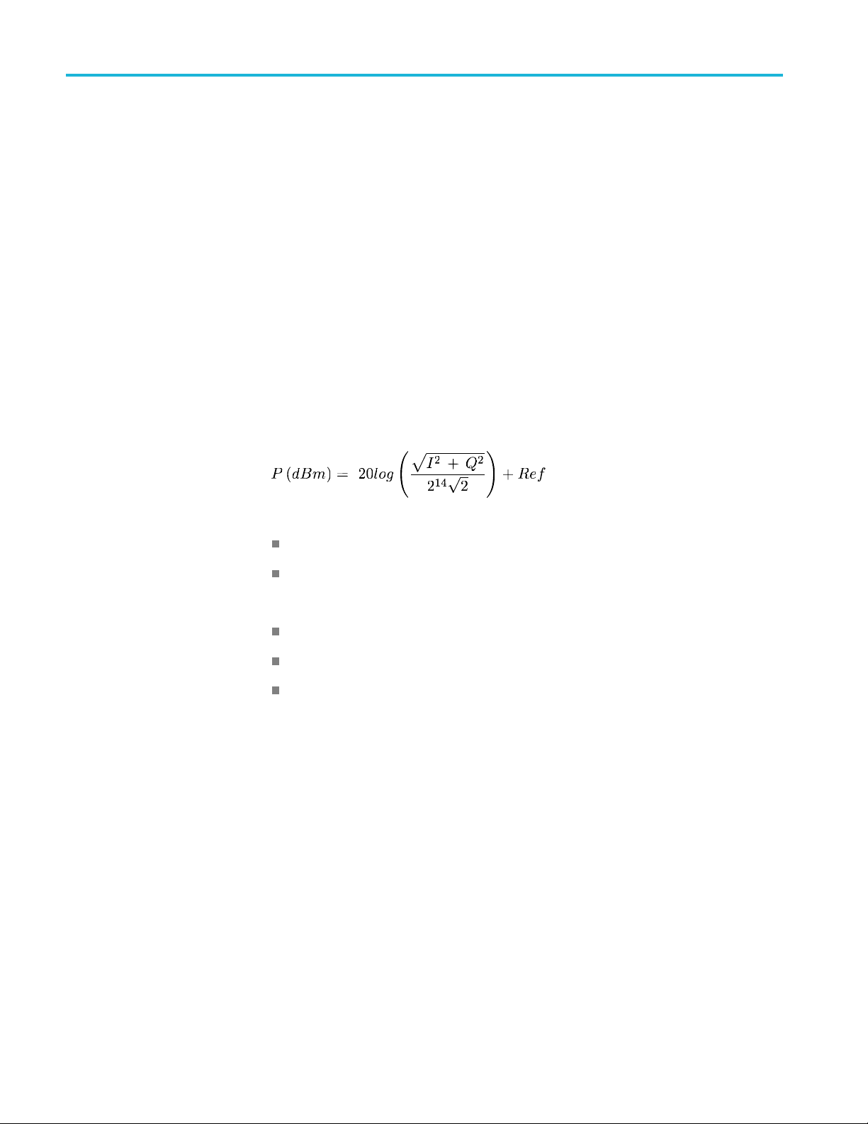
Specifications
Digital IQ Output Scaling
The duty cycle o
values to a very small percentage at the narrowest SPAN values. (See Table 68.)
At a SPAN of 100 Hz, the duty cycle will be 0.00038%; here, the EXT_IQ_DAV
signal is active (high) for 20 ns, and then inactive (low) for ≈5.28 ms.
The length of time that the EXT_IQ_DAV signal is inactive can be used to
determine if the RSA5100B is performing an alignment or a control change. If
the EXT_IQ_DAV signal is inactive for longer than 10 ms, then the RSA5100B
digital I/Q output data stream has been interrupted.
External equipment used to detect the occurrence of a data interruption can
monitor the state of the EXT_IQ_DAV signal. If the EXT_IQ_DAV signal is
inactive
duration of the data interruption can be determined by measuring the time between
successive EXT_IQ_DAV pulses.
Output p
Where:
Where:
for 10 ms or more, an alignment or control change has occurred. The
ower in dBm for a sinusoidal input
f the EXT_IQ_DAV signal varies from 100% at the widest SPAN
I and Q are the digital values at the Digital IQ output port
Ref = Reference Level
Valid for center frequencies that exceed:
Center frequency ≥ 80 MHz for Spans > 40 MHz
Center freq
Center frequency ≥ 2 MHz for Spans < 312.3 kHz
uency ≥ 30 MHz for Spans > 312.5 kHz and ≤ 40 MHz
70 RSA5100B Series Technical Reference
Page 85

Performance Verification
NOTE. The performance verification procedure is not a calibration procedure.
The performa
key specifications. For your instrument to be calibrated, it must be returned to a
Tektronix service facility.
nce verification procedure only verifies that your instrument meets
Prerequis
ites
The tests in this section make up an extensive, valid confirmation of performance
and functionality when the following requirements are met:
The cabinet must be installed on the instrument.
The instrument must have passed the Power On Self Tests (POST).
The instrument must have been last adjusted at an ambient temperature
between +18 °C (+64 °F) and +28 °C (+82 °F), must have been operating
forawarm-upperiodofatleast20minutes after starting the RSA5100B
application, and must be operating at an ambient temperature. (See Table 63
e63.)
on pag
Required Equipment
rocedures, use external, traceable signal sources to directly check warranted
The p
characteristics. (See page 75, Warranted Char acteristics Tests.) The following
table lists the equipment required for this procedure.
Table 70: Equipment required for Performance Verification
Item number and Minimum requirements Example Purpose
1. Frequency
Counter
2. RF Power Meter Agilent E4418B
3. RF Power Sensor19 kHz to 18 GHz RF Flatness: <3% Calibration
4. RF Power Sensor210 MHz to 26.5 GHz RF Flatness Agilent E4413A, Option
5. Signal Generator Frequency Accuracy: ±3 x 10⁻⁷Output
Frequency Range: 10 MHz; Accuracy: 1 x 10
factor data uncertainty: <2% (RSS)
Frequency: 0 to 40 GHz
–9
Agilent 53132A
Option 10
Agilent E9304A
Option H18
H10
Anritsu MG3694B
Options 2A, 3A, 4, 15A,
16, 22, SM5821
Checking reference
output frequency
accuracy
Adjusting signal
generator output level,
checking reference
output power level
Checking RF flatness,
intermodulation
distortion, image
suppression, and
external reference
lock check.
RSA5100B Series Technical Reference 71
Page 86

Performance Verification
Table 70: Equipment required for Performance Verification (cont.)
Item number and Minimum requirements Example Purpose
6. RF Signal
Generator
7. Precision
Attenuator
8. Power Splitter
9. Power Combiner
10. Low Pass Filters
(2)
11. Voltmeter
12. BNC Cable 50 , 36 in. male to male BNC connectors Signal interconnection
13. 3.5 mm -3.5 mm
Cable
14. N-SMA Cable 50 , 36 in. male N to male SMA connectors S ignal interconnection
15. Termination,
Precision 50
16. N-Female to BNC
male Adapter
17. 3.5 m m (F)
to 3.5 mm (F)
coaxial adapter
18. N-3.5mm cable
19. N-Male to 3.5 mm
male adapter
20. 3.5 mm
attenuator
Output Frequency 10 MHz to 26.5 GHz
Phase Noise at Center Frequency = 1 GHz
Offset
10 Hz
100 Hz
1kHz
10 kHz
100 kHz
1MHz
30 dB
<3 dB loss DC –3 GHz
>50 dB rejection 4 GHz to 14 GHz
Capable of measuring 30 VDC Standard Equipment Checking Noise Source
50 , 36 in. male to male 3.5 mm connectors Signal interconnection
Impedance: 50 3.5 mm male Signal interconnection
50 , 36 in. male N to male 3.5 mm connectors
3 dB (two required)
SSB Phase Noise (F) dBc/Hz
–71
–93
–118
–121
–119
–138
Anritsu MG3694B
Options 2A, 3A, 4, 15A,
16, 22, SM5821
Agilent 11667B Adjusting signal
Anritsu 2089-6208-00
Tektronix part number
103-0058-00
Tektronix part number
131-8508-00
Midwest Microwave
ATT-0550-03-35M-02
Checking phase
noise and third
order intermodulation
distortion
generator output level
Checking
intermodulation
distortion
Checking third order
intermodulation
distortion
Checking Zero-Span
Output
N cable to RSA5100B
connections
Checking third order
intermodulation
distortion
72 RSA5100B Series Technical Reference
Page 87

Performance Verification
Table 70: Equipment required for Performance Verification (cont.)
Item number and Minimum requirements Example Purpose
21. Planar Crown RF
Input Connector
-3.5mm
(RSA5115B,(RSA5126B
only)
22. Planar Crown RF
Input Connector
–TypeN
(RSA5103B,
RSA5106B only)
Tektronix part number
131-9062-00
Tektronix part number
131-4329-00
NOTE. You may need more adaptors than come with the instrument.
NOTE. Always use the Planar Crown adaptor that comes with the
RSA5115B/5126B instruments to connect to other equipment. Use a proper
adaptor when connecting cables with a different connector type.
Preliminary Checks
Fan Check
Warm-up
NOTE. Be sure that any adaptor and cable you use is specified to operate at the
frequency range of the test you are performing.
These steps should be performed before proceeding to the Warranted
Characteristics tests.
ug in the RSA5100B, power it on, and check that the fans located on the left
Pl
side of the instrument are operating.
CAUTION. Turn the RSA5100B off immediately if the fans are not operating.
Operating the Signal Analyzer without fans will damage the instrument.
Make sure the RSA5100B application is running, and allow the instrument to
warm up for at least 20 minutes.
NOTE. The fans will slow down and be quieter when the application is started;
this is normal. Fan speed may vary while the application is running, depending
on the internal temperature detected by the instrument.
RSA5100B Series Technical Reference 73
Page 88

Performance Verification
Touch S creen Check
Diagnostics
Check that the t
1. Verify that the touch screen is enabled (To uch S cr ee n O ff button is not
lighted).
2. Use your finger or a stylus to touch several of the on-screen touchable
readouts, such as RBW or Span, and verify they become active when touched.
Run a complete Diagnostics test session:
1. Select To o
2. Select the All Modules, All Tests checkbox at the top of the list.
3. Touch th e RUN button. The diagnostics tests will take some time to complete,
and some of them are interactive:
a. Noise Source Drive 28VDC Out diagnostic will ask you to test the noise
source output on the RSA5100B rear-panel.
b. The LED Check diagnostic will ask you to verify that all the highlighted
LEDs are turned on:
ouch screen detects touches:
ls > Diagnostics from the menubar.
Check with a voltmeter that the voltage is 28 V ±2 V.
Compare the LEDs highlighted in the diagnostic display with the
buttons on the front panel.
Press each of the keys and rotate the knob on the front panel. You
should see the corresponding key in the diagnostic display turn green.
Verify that each key is recognized.
Click the PASS or FAIL button when done.
c. The Display Pixel Test will ask you to look for video problems on the
test patterns:
Check the Green screen for any stuck or missing pixels. Any keypress,
click, or touch will move to the next screen.
Repeat with the Red screen, the Blue Screen, and the Gray scale
screen. Select Yes or No when the LCD Test dialog asks “Did you
see any video problems”.
4. When all diagnostics tests have completed, check that there is a check mark
beside each diagnostic name. An X instead of a check mark indicates that
the diagnostic had a failure.
5. Click the Diagnostics Failure Info tab and verify there is no failure
information listed.
6. Click the Exit Diagnostics button to exit diagnostics.
74 RSA5100B Series Technical Reference
Page 89
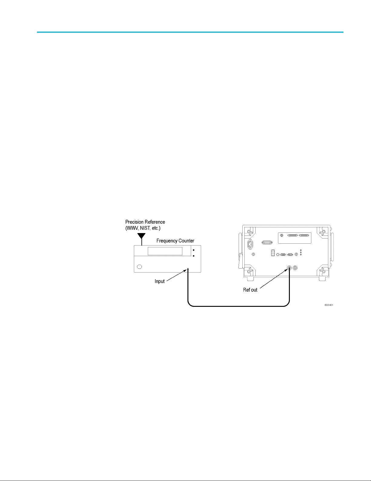
Performance Verification
Alignment
Warranted C
haracteristics Tests
Frequency Accuracy
Check Reference Output
Frequen
cy Accuracy
You should alig
Characteristics tests.
1. Select Alignm
2. Select Align Now. The alignment process will take a few minutes.
3. Verify that no alignment failures are reported in the status bar.
The following procedures verify the RSA5100B Series Signal Analyzer
performance is within the warranted specifications.
1. Connect Ref Out on the RSA5100B rear-panel through a 50 Ω precision
coaxial
2. Connect a precision frequency reference to the frequency counter.
n the instrument before proceeding with the Warranted
ents in the Too l s menu. The Alignments dialog box will open.
cable to the frequency counter input. See the following figure.
Figure 3: Connections for Reference Frequency Output Accuracy check
3. Set the Frequency counter:
Function Frequency
Gate time
4. Check that the frequency counter reads 10 MHz ±4 Hz (Option PFR). Without
Option PFR, check that the frequency counter reads 10 MHz +/- 40 Hz. Enter
he frequency in the test record.
t
RSA5100B Series Technical Reference 75
2s
Page 90

Performance Verification
Check Reference Output
Power Level
1. Set up the power
NOTE. Store the power sensor correction factors in the power meter, if you have
not yet done so.
a. Connect the power sensor to the Sensor input on the power meter, as
shown in the following figure.
Figure 4: Power meter s etup
b. Press Zero/Cal,andthenpressZERO on the power meter.
c. Connect the RF input of the power sensor to the power meter power
reference output, as shown in the following figure.
meter and sensor.
Figure 5: Power meter calibration
d. Press CAL to execute the calibration.
e. Disconnect the RF input of the power sensor from the power meter
reference output.
2. Connect the power sensor RF input to the Ref Out connector on the
RSA5100B rear-panel, using the N-female to BNC male adapter (see the
following figure).
3. Press Frequency/Cal Factor, and then set Freq to 10 MHz.
4. Check that the Ref Out signal is >0 dBm. Enter this level in the test record.
76 RSA5100B Series Technical Reference
Page 91
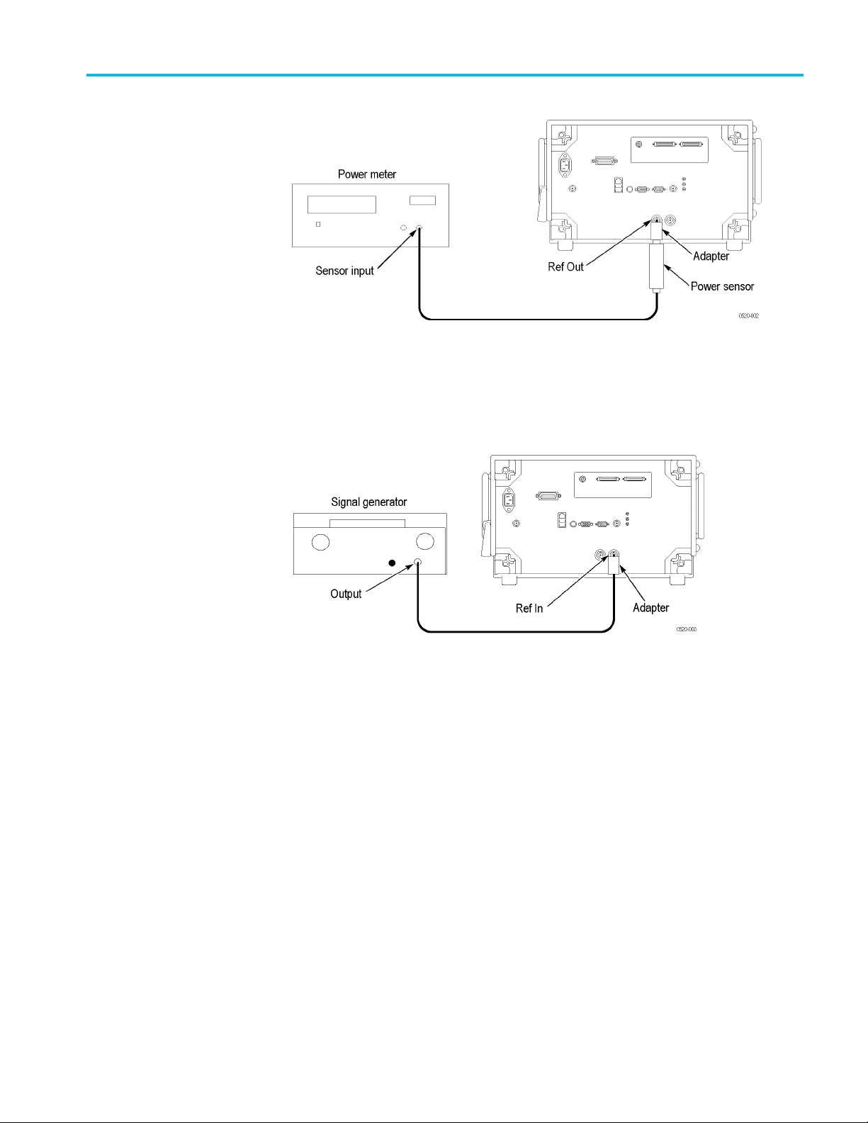
Performance Verification
Figure 6: Equipment connections for Ref Out power level check
External Referenc e Input
Level
1. Connect the signal generator output to the Ref In connector on the RSA5100B
rear panel, using a 50 Ω N-N coaxial cable and N-female to BNC male adapter
(see the following figure).
Figure 7: Equipment connections for Ref In power level check
2. Set the Signal generator controls:
Frequency 10 MHz
Level 0 dBm
RF
On
3. Set the RSA5100B to use the external reference:
a. Select Setup > Configure In/Out > Frequency Reference.
b. Select the External radio button.
4. Check the Input Reference limits:
a. Check that the Status Bar shows Ref: Ext.
b. Set the Source to Internal (10 MHz).
c. Set the signal generator output level to –10 dBm.
RSA5100B Series Technical Reference 77
Page 92

Performance Verification
d. Set the Source t
e. Check that the Status Bar shows Ref: Ext.
f. Set the Source to Internal (10 MHz).
g. Set the signal generator output level to +6 dBm.
h. Set the Source to External.
i. Check that the Status Bar shows Ref: Ext.
j. Disconnec
message should pop up to indicate loss of lock (see the following figure).
o External.
t the signal generator from the Ref In connector. An error
k. Click OK on the error message, and check that the Status Bar shows
Ref: Int.
l. Enter Pass or Fail in the test record.
m. Repeat the test at 100 MHz, beginning with step 2.
Phase Noise (Instruments with Option 11)
If Option 11 is installed in your instrument, use the following procedure to check
the phase noise. If Option 11 is not installed in your instrument, use the procedure
that follows. (See page 80, Phase Noise (Instruments without Option 11).)
NOTE. The intent of the Phase Noise test is to measure the phase noise level of the
strument. The phase noise specification does not cover residual spurs. If the
in
specific measurement frequency results in measuring a residual spur that is visible
above the noise level, the phase noise specification applies not to the spur but to
the noise level on either side of the spur. Please refer to the Spurious Response
specifications. (See Table 20.) Also, refer to the Spurious Response section of this
procedure to determine whether or not a residual spur is within the specification.
(See page 124, Spurious Response.)
78 RSA5100B Series Technical Reference
Page 93

Performance Verification
1. Connect the gen
erator output to the RTSA RF Input, using a 50 Ω coaxial
cable (see the following figure).
Figure 8: Equipment connections for phase noise checks
2. Reset the RSA5100B to factory defaults: select Setup > Preset (Main) from
the Setup menu.
3. Select To ol s > Alignments andthenselectAlign Now.
4. Modify the default settings:
Center Frequency
Setup > Settings > Freq & Span > Center
Span
Setup > Settings > Freq & Span > Span
Ref Level
Setup > Amplitude > Internal Settings > Ref Level
RF & IF Optimization
Setup > Amplitude > Internal Settings > RF & IF
Optimization
5. Set the generator as follows:
Center Frequency 1.00 GHz
Output level
RF
+5 dBm
On
6. Select Run > Run Single to stop acquisitions.
7. Display the Phase Noise measurement:
Select Setup > Displays.
Select the RF Measurements folder.
1.00 GHz
1MHz
+5 dBm
Maximize Dynamic Range
Select the Phase Noise display and select Add.
RSA5100B Series Technical Reference 79
Page 94

Performance Verification
Select the Spec
Select OK.
8. Select Setup > Settings to display the Phase Noise settings control panel.
9. On the Frequency tab, set the Start Offset to 1 kHz for both the Measurement
BW and the Integration BW.
10. Set the Stop Offset to 10 MHz for both the Measurement BW and the
Integration BW.
11. Select the Parameters tab.
12. Set the Average value to 20 and click the check box to enable averaging.
13. Select the Traces tab.
14. Select T
so that Trace 2 is not be displayed.
15. Select
the Marker readout on the left side of the graph. Set the Marker value to
6MHz.
16. Press the Single key and wait for 20 averages to complete.
race 2 in the Trace drop-down list. Deselect the Show checkbox
Trace 1 from the trace drop-down list above the graph display. Select
trum display and select Remove.
17. Read t
18. Document the test results in the test record at each frequency.
he value for the 6 MHz offset from the Offset readout.
Phase Noise (Instruments without Option 11)
Check Phase Noise
If Option 11 is not installed in your instrument, use the following procedure
check the phase noise. If Option 11 is installed in your instrument, use the
to
preceding procedure. (See page 78, Phase Noise (Instruments with Option 11).)
NOTE. The intent of the Phase Noise test is to measure the phase noise level of the
instrument. The phase noise specification does not cover residual spurs. If the
specific measurement frequency results in measuring a residual spur that is visible
above the noise level, the phase noise specification applies not to the spur but to
the noise level on either side of the spur. Please refer to the Spurious Response
specifications. (See Table 20.) Also, refer to the Spurious Response section of this
procedure to determine whether or not a residual spur is within the specification.
(See page 124, Spurious Response.)
80 RSA5100B Series Technical Reference
Page 95

Performance Verification
1. Connect the gen
erator output to the RTSA RF Input, using a 50 Ω coaxial
cable (see the following figure).
Figure 9: Equipment connections for phase noise checks
2. Reset the RSA5100B to factory defaults: Select Setup > Preset (Main) from
the Setup menu.
3. Press Tools > Alignments and then select Align Now.
4. Modify the settings:
Center Frequency
Setup > Settings > Freq & Span > Center
Span
Setup > Settings > Freq & Span > Span
VBW
Setup > Settings > BW > VBW
Detection
Setup > Settings > Traces > Detection
Function
Setup > Settings > Traces > Function
Count
Setup > Settings > Traces > Count
Trace Points
Setup > Settings > Prefs > Trace Points
RF & IF Optimization
Setup > Amplitude > Internal Settings > RF & IF
Optimization
Reference level
Setup > Amplitude > Internal Settings > Ref Level
5. Set the generator as follows:
1.00 GHz
1MHz
10 Hz (box checked)
Avg (VRMS)
Avg (VRMS)
100 (box checked)
2401
Maximize Dynamic Range
+5 dBm
RSA5100B Series Technical Reference 81
Page 96

Performance Verification
Frequency
Output level
RF
1.00 GHz
+5 dBm
On
6. Turn on the Reference Marker (MR) and Marker 1 (M1), and set them for
Delta operation and Noise Mode (dBc/Hz).
a. Select Markers located at the bottom right of the screen on the status bar
to display the Markers control bar.
b. Click the down arrow on the left side of the Markers control bar to view
the Select a Marker dropdown menu. Select Add Marker to add the
MR marker.
c. Select Add Marker againtoaddtheM1marker.
d. Select Define located on the right side of the Markers control bar to open
the Define Markers control panel.
e. Select Delta from the Readouts drop down menu and check the dBc/Hz
check box.
7. For each span shown in the following table, perform steps a through f below:
Table 71: Phase noise offsets (Low range; without Option 11)
CF +
CF +
+ 100 kHz
CF
fset
1kHz
10 kHz
Span M1 Of
4kHz
40 kHz
300 kHz
a. Press the Span key and enter a Span value from the table.
elect Run > Run Single.
b.S
c. Select the Reference Marker (MR) using the Select a Marker dropdown
enu on the Marker control bar and then click the Peak key.
m
d. Select Marker 1 (M1).
e. Set the Marker 1 (M1) frequency by entering the offset value from the
table above in the Frequency box on the right side of the Markers control
bar.
f. Read the marker noise level in dBc/Hz in the Delta Marker readout (upper
right corner of the screen), and enter the value in the test record. (Limits
are shown in the test record.)
8. Select Absolute from the Readouts dropdown menu. This disables dBc/Hz
and sets units to dBm/Hz.
82 RSA5100B Series Technical Reference
Page 97

Performance Verification
9. Record the gene
a. Select the Reference Marker (MR) and then click the To C e nt er key to
center the MR marker on the peak of the 1000 MHz signal.
b. Record the MR Marker amplitude (upper-left corner of the screen). This
value is called Carrier Power and is used below.
10. Obtain the phase noise at 1 MHz offset. Start by setting the RSA5100B to the
settings listed below:
a. Center Frequency (Freq key): 1001 MHz
b. Span (Span key): 10 kHz
c. Reference Level Offset: -30 dBm (This is the amplitude control in the
upper left of the display.)
d. Set input attenuation for manual control:
Select Setup > Amplitude > Internal Settings.
Deselect the Internal Attenuator Auto check box.
Set Internal Attenuator to 0 dB.
11. Select Run > Run Single.
12. Center the M1 marker in the middle of the screen:
rator signal amplitude in the Test Record:
Select Marker 1 (M1).
Select Readouts > Power in the Define Markers control panel.
Set the M1 frequency to 1001 MHz using the Frequency field on the
Marker control bar.
The marker is now located at the center frequency position.
13. Read the noise amplitude on Marker M1 in dBm/Hz.
14. Subtract the value of MR obtained in step 9 to obtain the phase noise
amplitude at 1 MHz.
Forexample,ifMR=4.7dBmandM1=–129.6dBm/Hz,thenM1-MR
–134.3 dBc/Hz.
15. Enter the value obtained at 1 MHz in the test record for phase noise at 1 MHz.
16. Obtain the phase noise at 6 MHz offset. Start by setting the RSA5100B to the
settings listed below:
a. Center Frequency (Freq key): 1006 MHz.
b. Span (Span key): 10 kHz.
c. Select Run > Run Single.
d. Set the Marker M1 Frequency to 1006 MHz.
=
RSA5100B Series Technical Reference 83
Page 98

Performance Verification
e. Read the noise l
f. Subtract the value of Carrier Power obtained in step 9 in order to obtain
the phase nois
For example, if Carrier Power = 4.7 dBm and M1 = –145.1 dBm/Hz, then
M1–Carrier
g. Enter the value obtained at 6 MHz in the test record for phase noise at
6MHz.
17. Obtain the phase noise at 10 MHz offset. Start by setting the RSA5100B
to the sett
a. Center Frequency (Center key): 1010 MHz.
b. Span (Span key): 10 kHz.
c. Select Run > Run Single.
d. Set the Marker Frequency to 1010 MHz.
NOTE. The intent of the Phase Noise test is to measure the phase noise level of
the instrument. The phase noise specification does not cover residual spurs. If
the specific measurement frequency results in measuring a residual spur that
is vis
the spur but to the noise level on either side of the spur. Please refer to the
Spurious Response specifications. (See Table 20.) Also, refer to the Spurious
Response section of this procedure to determine whether or not a residual spur
is within the specification. (See page 124, Spurious Response.)
ings below:
ible above the noise level, the phase noise specification applies not to
evel on Marker M1 in dBm/Hz.
e amplitude at +6 MHz.
Power = –149.8 dBc/Hz.
e. Read the noise amplitude on marker M1 in dBm/Hz.
f. Subtract the value of the Carrier Power marker obtained in step 9 to obtain
the phase noise amplitude at +10 MHz.
For example, if Carrier Power = 4.7 dBm and M1 = –146.1 dBm/Hz,
Then M1-Carrier Power = –150.8 dBc/Hz.
g. Enter the value obtained at 10 MHz in the test record for phase noise
at 10 MHz.
84 RSA5100B Series Technical Reference
Page 99

Amplitude
Performance Verification
RF Flatness (Frequency
Response) 10 MHz to
26.5 GHz
1. Connect the RF generator, power splitter, power meter, and RSA5100B, as
shown in the following figure.
The power splitter outputs should connect directly to the RSA5100B RF Input
and to the Power Sensor, without using cables.
Figure 10: Equipment connections for RF flatness check
2. To record the test readings, you can make a printout of the following table.
(See Table 72.)
3. Reset the RSA5100B to factory defaults: Setup > Preset (Main).
4. Select To ol s > Alignments andthenselectAlign Now.
5. Set the RSA5100B as follows:
Level
Ref
Setup > Amplitude >Internal Settings > Ref Level
ternal Attenuator
In
Setup > Amplitude > Internal Settings > Internal
Attenuator
Span
etup > Settings > Freq & Span> Span
S
LF Path
etup > Acquire > Input Params
S
–15 dBm
10 dB (Auto unchecked)
1MHz
Use Low Freq... box unchecked
6. Set the RF signal generator for a -14 dBm output amplitude and turn RF On.
RSA5100B Series Technical Reference 85
Page 100

Performance Verification
7. Set both the RF s
ignal generator output frequency and the RSA5100B Center
Frequency to the first frequency in the RF Flatness table that follows. This is
the reference frequency. (See Table 72.)
8. Select the Peak key on the Markers control bar to set the Reference Marker
(MR) to the carrier peak.
9. Adjust the RF signal generator output level for a marker reading of –20
±0.5dBm.
10. Record the Power Meter reading and the RSA5100B marker reading in the
following table.
11. Set both the RF Generator output frequency and the RSA5100B center
frequency to the next frequency in the table.
12. Select the Peak key on the Markers control bar to set the Reference Marker
(MR) to the carrier peak.
13. Calculate the ΔPower Meter number: subtract the Power meter reading at
100 MHz from the Power Meter reading at this frequency.
14. Calculate the ΔRTSA number: subtract the RTSA reading at 100 MHz from
the RTSA reading at this frequency.
15. Calculate the RF Flatness Error:
RF Flatness Error = ΔRTSA at this freq – ΔPower Meter at this freq
Readings are in dBm, error is in dB.
16. Repeat items 11 through 15 for each of the center frequencies shown in the
RF Flatness table up to the maximum bandwidth of the device-under-test.
(See Table 72.)
Table 72: RF Flatness (Preamp OFF)
Attenuator = 10 dB
Power meter
Frequency
100 MHz 0 0 0
10 MHz
20 MHz
30 MHz
40 MHz
50 MHz
60 MHz
70 MHz
80 MHz
90 MHz
reading
∆ Power meter
(vs. 100 MHz) RTSA reading
∆ RTSA reading
(vs. 100 MHz)
RF flatness
1
error
86 RSA5100B Series Technical Reference
 Loading...