


xx
RSA5100A Series
Real-Time Signal Analyzer
ZZZ
Specifications and Performance Verification
Technical Reference
*P077052001*
077-0520-01


xx
RSA5100A Series
Real-Time Signal Analyzer
ZZZ
Specifications and Performance Verification
Technical Reference
Revision A
Warning
The servicing instructions are for use by qualified personnel
only. To avoid personal injury, do not perform any servicing
unless you are qualified to do so. Refer to all safety summaries
prior to performing service.
www.tektronix.com
077-0520-01

Copyright © Tektronix. All rights reserved. Licensed software products are owned by Tektronix or its subsidiaries
or suppliers, and are protected by national copyright laws and international treaty provisions.
Tektronix products are covered by U.S. and foreign patents, issued and pending. Information in this publication
supersedes that in all previously published material. Specifications and price change privileges reserved.
TEKTRONIX and TEK are registered trademarks of Tektronix, Inc.
Contacting Tektronix
Tektronix, Inc.
14150 SW Karl Braun Drive
P.O . B ox 5 00
Beaverto
USA
For product information, sales, service, and technical support:
n, OR 97077
In North America, call 1-800-833-9200.
World wi d e, v i si t www.tektronix.com to find contacts in your area.

Warranty
Tektronix warrants that this product will be free from defects in materials and workmanship for a period of one (1)
year from the date of shipment. If any such product proves defective during this warranty period, Tektronix, at its
option, either will repair the defective product without charge for parts and labor, or will provide a replacement
in exchange for the defective product. Parts, modules and replacement products used by Tektronix for warranty
work may be n
the property of Tektronix.
ew or reconditioned to like new performance. All replaced parts, modules and products become
In order to o
the warranty period and make suitable arrangements for the performance of service. Customer shall be responsible
for packaging and shipping the defective product to the service center designated by Tektronix, with shipping
charges prepaid. Tektronix shall pay for the return of the product to Customer if the shipment is to a location within
the country in which the Tektronix service center is located. Customer shall be responsible for paying all shipping
charges, duties, taxes, and any other charges for products returned to any other locations.
This warranty shall not apply to any defect, failure or damage caused by improper use or improper or inadequate
maintenance and care. Tektronix shall not be obligated to furnish service under this warranty a) to repair damage
result
b) to repair damage resulting from improper use or connection to incompatible equipment; c) to repair any damage
or malfunction caused by the use of non-Tektronix supplies; or d) to service a product that has been modified or
integrated with other products when the effect of such modification or integration increases the time or difficulty
of servicing the product.
THIS WARRANTY IS GIVEN BY TEKTRONIX WITH RESPECT TO THE PRODUCT IN LIEU OF ANY
OTHER WARRANTIES, EXPRESS OR IMPLIED. TEKTRONIX AND ITS VENDORS DISCLAIM ANY
IMPLIED WARRANTIES OF MERCHANTABILITY OR FITNESS FOR A PARTICULAR PURPOSE.
TRONIX' RESPONSIBILITY TO REPAIR OR REPLACE DEFECTIVE PRODUCTS IS THE SOLE
TEK
AND EXCLUSIVE REMEDY PROVIDED TO THE CUSTOMER FOR BREACH OF THIS WARRANTY.
TEKTRONIX AND ITS VENDORS WILL NOT BE LIABLE FOR ANY INDIRECT, SPECIAL, INCIDENTAL,
OR CONSEQUENTIAL DAMAGES IRRESPECTIVE OF WHETHER TEKTRONIX OR THE VENDOR HAS
ADVANCE NOTICE OF THE POSSIBILITY OF SUCH DAMAGES.
[W2 – 15AUG04]
btain service under this warranty, Customer must notify Tektronix of the defect before the expiration of
ing from attempts by personnel other than Tektronix representatives to install, repair or service the product;


Table of Contents
General Safety Summary .......................................................................................... v
Preface ............................................................................................................. vii
Related Manuals .............. ................................ .................................. ............. vii
Specificati
Performance Verification ............... ................................ .................................. ........ 47
ons ....................................................................................................... 1
Performance Conditions ...................................................................................... 1
Electrical Specifications.......................... .................................. ........................... 1
Electrical Functional Specifications .......................... ................................ .............. 27
Physical Characteristics...................................................................................... 38
Safety........................................................................................................... 39
Certific
Environmental Characteristics .............................................................................. 39
Digital IQ Output Connector Pin Assignment (Option 55 Only)............ ............................ 41
Digital IQ Output Timing .................................................................................... 44
Prerequisites ....................... .................................. ................................ .......... 47
Requ
Preliminary Checks................................... ................................ ........................ 49
Warranted Characteristics Tests ............................................................................. 51
Frequency Accuracy.......................................................................................... 51
Phase Noise (Instruments with Option 11)................................................................. 54
Phase Noise (Instruments without Option 11)............................................................. 56
RF
Amplitude ..................................................................................................... 64
Noise and Distortion.......................................................................................... 79
IF Flatness (Channel Response)................... .................................. ........................ 87
Spurious Response........................ ................................ ................................ .... 90
Test Record.............. ................................ .................................. .................... 98
ations and Compliances ............................................................................. 39
ired Equipment.......................................................................................... 47
Input.......................................... .................................. ............................ 61
RSA5100A Series Technical Reference i

Table of Contents
List of Figure
Figure 1: Digital IQ output connector pin assignment ........................................................ 41
Figure 2: IQ
Figure 3: Connections for Reference Frequency Output Accuracy check .................................. 51
Figure 4: Power meter setup ................. ................................ .................................. .. 52
Figure 5: Power meter calibration ... .................................. ................................ .......... 52
Figure 6: Equipment connections for Ref Out power level check ........................................... 53
Figure 7: Equipment connections for Ref In power level check ............. ................................ 53
Figure 8:
Figure 9: Equipment connections for phase noise checks .................................................... 55
Figure 10: Equipment connections for phase noise checks................... ................................ 57
Figure 11: Equipment connections for VSWR check ......................................................... 61
Figure 12: Equipment connections for RF Flatness check............ ................................ ........ 64
Figure 13: Equipment connections for Low Frequency (LF) input path accuracy check ................. 68
e 14: Equipment connections for RF Flatness (Frequency Response) 10 MHz to 6.2 GHz check. 71
Figur
Figure 15: Equipment connections for Low Frequency (LF) input path accuracy check ................. 75
Figure 16: Equipment connections for Third Order Intermodulation Distortion check . .. ... . .... .. ... . .. 79
Figure 17: Equipment connections for IF Flatness check..................................................... 87
Figure 18: Equipment connections for Image Suppression check . .................................. ........ 92
Figure 19: Equipment connections for Signal Spurious check ............................................... 94
Timing............................................................................................... 45
Error message showing loss of lock to External Reference signal ......................... ...... 54
s
ii RSA5100A Series Technical Reference

List of Tables
Table 1: Frequency ................................................................................................. 1
Table 2: Phase noise................................................................................................ 2
Table 3: Integrated jitter . . ... . .... . . ... . ... . ... . . . ... . ... . ... . . . ... . ... . ... . .... .. ... . ... . .... . . ... . ... . ... . . . ... . . 3
Table 4: RF input........ .................................. ................................ ......................... 3
Table 5: Maximum input level ............... ................................ ................................ ..... 4
Table 6: Input attenuator........................................................................................... 4
Table 7: Analog sweep.................. .................................. ................................ ......... 4
Table 8: Amplitude and RF flatness (exc
Table 9: Noise and distortion........................... ................................ ........................... 6
Table 10: Channel Response – Amplitude & Phase Flatness (Standard/Option 40) . .... .. ... . .... .. ... . ... 7
Table 11: Channel Response – Amplitude & Phase Flatness (Option 85) ...................... ............. 8
Table 12: Channel response
Table 13: Channel response (center frequency ≤3.0 GHz)
Table 14: Channel response (3.0 GHz < center frequency ≤ 6.2 GHz)
Table 15: Channel response (LF band, 11 MHz < center frequency ≤ 22 MHz;)
Table 16: Pulse measurements, typical.......................................................................... 10
Table 17: Impulse response ...................................................................................... 14
Table 18: Spurious response........ ................................ ................................ .............. 14
Table 19: Spurious response with signal at center frequency (offset ≥ 400 kHz) .......................... 15
Table 20: Spurious response with signal at center frequency (10 kHz ≤ offset ≤ 400 kHz).............. 16
Table 21: Spurious response with signal at other than CF .................................................... 16
Table 22: Acquisition . . ... . ... . ... . . . ... . ... . ... . ... . .... . . ... . ... . ... . ... . .... . . ... . ... . ... . ... . .... .. ... . ... . ... 16
Table 23: Amplitude vs. time . .. ... . ... . ... . ... . ... . ... . ... . ... . ... . ... . .... . . ... . ... . ... . ... . ... . ... . ... . ... . ... 18
Table 24: Trigger .................................................................................................. 18
Table 25: Trigger (without Option 200)................................... ................................ ...... 20
Table 26: Trigger (with Option 200) ............................................................................ 21
Table 27: Resoluti
Table 28: Range and settable RBW (SA mode)...................... ................................ .......... 24
Table 29: Resolution bandwidth filter (time-domain mode).................................................. 25
Table 30: Range and settable RBW (time-domain mode) .................................................... 25
Table 31: Preamp (Option 50) ................. ................................ ................................ .. 26
Table 32: Digital IQ output....................................................................................... 26
Table 33: 28 Volt noise source drive output .................................................................... 26
Table 34: Measurement function ................................................................................ 27
Table 35: Views by domain ...................................................................................... 29
Table 36: Analog demodulation accuracy .......... ................................ ............................ 29
Table 37: General Purpose Analog modulation accuracy............................. ........................ 30
Table 38: General purpose digital modulation analysis (Option 21)......................................... 31
Table of Contents
luding mismatch error)
1
...................................................................................... 8
1
............................................ 4
1
........................ ........................... 9
1
........................ ............. 9
1
......................... 10
on bandwidth filter (SA mode) ............................. ................................ 24
RSA5100A Series Technical Reference iii

Table of Contents
Table 39: Digit
al demodulation accuracy (Option 21) ................ ................................ ........ 31
Table 40: ACLR measurement................................................................................... 33
Table 41: Digital phosphor spectrum processing (DPx) ........ ................................ .............. 33
Table 42: Frequency Settling Time Measurement (Option 12)
1
............................................. 35
Table 43: OBW measurement.......... .................................. ................................ ........ 36
Table 44: xdB Bandwidth Measurement........................................................................ 36
Table 45: Se
ttled Phase Uncertainty (Option 12)
1
............................................................. 36
Table 46: File Saving Speeds .................................................................................... 36
Table 47: Data Transfer/Measurement Speeds....... .................................. ........................ 37
Table 48: Physical characteristics ... ................................ .................................. .......... 38
Table 49: Display/computer................ ................................ .................................. .... 38
Table 50: Environmental characteristics ........................................................................ 39
Table 51
: Power requirements ............... .................................. ................................ .. 40
Table 52: I OUTPUT connector pin assignment................... ................................ ............ 41
Table 53: Q OUTPUT connector pin assignment.............................................................. 42
Table 54: Mating connections.............. .................................. ................................ .... 44
Table 55: EXT_IQ_DAV Duty cycle versus Span............................... .............................. 44
Table 56: IQ Timing............................................................................................... 45
e 57: Equipment required for Performance Verification ............... ................................ .. 47
Tabl
Table 58: Phase noise offsets (Low range; without Option 11) ........ ................................ ...... 58
Table 59: RSA5103A VSWR Test Frequencies (MHz)....................................................... 62
Table 60: RSA5106A VSWR Test Frequencies (GHz) ....................................................... 62
Table 61: RSA5100A VSWR Preamp On Test Frequencies (MHz)......................................... 62
Table 62: RSA5106A VSWR Preamp On Test Frequencies (GHz) ......................................... 63
ble 63: RF Flatness (Preamp OFF) ........................................................................... 65
Ta
Table 64: Low Frequency Input Path Flatness (Preamp OFF) ............................................... 69
Table 65: RF Flatness (Option 50 Preamp ON).... ................................ ............................ 72
Table 66: Low Frequency Input Path Flatness (Preamp ON)................................................. 76
Table 67: Frequencies of interest for DANL (LF Path) ....................................................... 82
Table 68: Frequencies of interest for DANL (RF Path) ....................................................... 83
Table 69: Frequencies of interest for DANL LF Path check (Option 50) ................................... 85
Table 70: Frequencies of interest for DANL check (Option 50) ........................... .................. 86
Table 71: IF Flatness.............. .................................. ................................ .............. 88
Table 72: Residual Response Center Frequencies ........... ................................ .................. 91
Table 73: Image Suppression Settings .. .. ... . ... . .... . . ... . ... . ... . ... . ... . .... .. ... . ... . ... . ... . ... . .... . . ... . 93
Table 74: Center Frequencies for Half-IF. . ... . ... . .... .. ... . ... . .... .. ... . ... . .... .. ... . ... . . . ... . ... . .... .. ... 97
iv RSA5100A Series Technical Reference

General Safety Summary
General Safet
To Avoid Fire or Personal
Injury
ySummary
Review the fo
this product or any products connected to it.
To avoid pot
Only qualified personnel should perform service procedures.
While using this product, you may need to access other parts of a larger system.
Read the safety sections of the other component manuals for warnings and
cautions r
Use proper power cord. Use only the power cord specified for this product and
certified for the country of use.
Ground the product. This product is grounded through the grounding conductor
of the power cord. To avoid electric shock, the grounding conductor must be
connected to earth ground. Before making connections to the input or output
terminals of the product, ensure that the p roduct is properly grounded.
Observe all terminal ratings. To avoid fire or shock h azard, observe all ratings
and markings on the product. Consult the product manual for further ratings
information before making connections to the product.
llowing safety precautions to avoid injury and prevent damage to
ential hazards, use this product only as specified.
elated to operating the system.
The inputs are not rated for connection to mains or Category II, III, or IV circuits.
Power disconnect. The power cord disconnects the product from the power source.
Do not block the power cord; it must remain accessible to the user at all times.
Do not operate without covers. Do not operate this product with covers or panels
removed.
Do not operate with suspected failures. If you suspect that there is damage to this
product, have it inspected by qualified service personnel.
Avoid exposed circuitry. Do not touch exposed connections and components when
power is present.
Replace batteries properly. Replace batteries only with the specified type and
rating.
Use proper fuse. Use only the fuse type and rating specified for this product.
Wear eye protection. Wear eye protection if exposure to high-intensity rays or
laser radiation exists.
RSA5100A Series Technical Reference v
General Safety Summary
TermsinThisManual
Symbols and Terms on the
Product
Do not operate i
Do not operate in an explosive atmosphere.
Keep product surfaces clean and dry.
Provide prop
on installing the product s o it has proper ventilation.
These terms may appear in this manual:
WARNING.
in injury or loss of life.
CAUTION
damage to this product or other property.
These t
erms may appear on the product:
DANGER indicates an injury hazard immediately accessible as you read
the ma
n wet/damp conditions.
er ventilation. Refer to the manual's installation instructions for details
Warning statements identify conditions or practices that could result
. Caution statements identify conditions or practices that could result in
rking.
WARNING indicates an injury hazard not immediate l y accessible as you
the marking.
read
CAUTION indicates a hazard to property including the product.
The following symbol(s) may appear on the product:
vi RSA5100A Series Technical Reference

Preface
Related Manuals
This document contains the Specifications and the Performance Verification for
the RSA5100A Series Real Time Spectrum An alyzers. It contains procedures
suitable for
meets the performance characteristics as warranted.
The following documents relate to the operation or service of the analyzer:
determining that the analyzer functions, is adjusted properly, and
The RSA61
Real-Time Signal Analyzers Quick Start User Manual describes how to use
your analyzer.
The RSA6100A Series Real-Time Spectrum Analyzers, RSA5100A Series
Real-Time Signal Analyzers Application Examples Manual, provides tutorial
examples of how to take measurements in different application areas.
The RSA6100A Series Real-Time Spectrum Analyzers, RSA5100A Series
Real-Time Signal Analyzers Programmers Manual describes how to use a
computer to control the analyzer through the GPIB interface.
The RSA5100A Series Service Manual provides information for maintaining
and servicing your analyzer to the module level.
00A Series Real-Time Spectrum Analyzers, RSA5100A Series
RSA5100A Series Technical Reference vii

Preface
viii RSA5100A Series Technical Reference

Specifications
This section lists the RSA5100A Series Real Time-Signal Analyzer specifications.
Items listed in the Performance Requirement column are generally quantitative,
and are eithe
by design. Items listed in the Reference Information column are useful operating
parameters that have typical values; information in this column is not guaranteed.
NOTE. In these tables, characteristics which are warranted are indicated by a
symbol in the Characteristics column.
Performance Conditions
rtestedbythePerformance Verification procedure or are guaranteed
The perf
ormance limits in these specifications are valid with these conditions:
The signal analyzer must have been calibrated and adjusted at an ambient
temper
ature between +20 °C and +30 °C.
The signal analyzer must be in an environment with temperature, altitude,
humidi
ty, and vibration within the operating limits described in these
specifications.
gnal analyzer must have had a warm-up period of at least 20 minutes
The si
after starting the RSA5100A application.
Electrical Specifications
Table 1: Frequency
Characteristic Description
Measurement frequency
Frequency
range, nominal
Frequency
Marker
Residual FM, typical
Span Accuracy ±0.3% of span (Auto mode)
RSA5103A (RF band) 9 kHz to 3 GHz
RSA5106A (RF band) 9 kHz to 6.2 GHz
Readout Accuracy
Readout Resolution
±(RE × MF + 0.001 × Span + 2 ) Hz
RE: Reference Frequency Error
MF: Marker Frequency [Hz]
Reference level dependent
As small as 0.0001 µV
<2 Hz
Freq vs Time mode, Autoscale (95% confidence)
in 1 s econd at 200 MHz CF, 100 Hz span,
p-p
RSA5100A Series Technical Reference 1

Specifications
Table 1: Frequency (cont.)
Characteristic Description
Reference Frequency
–8
Stability, nominal
Adjustment Range ±5.5 x 10
Initial Accuracy at Cal
Aging
Per day
Long term
Cumulative Error, typical
ature + Aging)
Internal or External
ature drift
Temper
nce
Refere
Output Level
(Temper
Internal or External, typical +4 dBm
External Reference Input, nominal BNC Connector, 50 Ω
External Reference Input Frequency, nominal 10 MHz ±30 Hz (3 ppm)
External Reference Input Range
External Reference Input Level
2x10
–7
Within 1 x 10
–9
±1 x 10
±3 x 10
4x10
1x10
(after 30 days of operation)
–7
–7
(10 years)
–7
(10°Cto40°C)
>0 dBm
Spurious level on input signal must be <–80 dBc within
100 kHz offset to avoid on-screen spurious
–7
±3 x 10
–10 dBm to +6 dBm
–7
(after a 10 min warmup)
(10 years)
Table 2: Phase noise
Characteristic Description
Specified
Frequency =
1000 MHz
Typical
Frequency =
1000 MHz
Noise sideband
–103 dBc/Hz
09 dBc/Hz
–1
–112 dBc/Hz
–130 dBc/Hz
137 dBc/Hz
–
–137 dBc/Hz
–107 dBc/Hz
–113 dBc/Hz
–116 dBc/Hz
–139 dBc/Hz
–144 dBc/Hz
–144 dBc/Hz
Offset
1kHz
10 kHz
0kHz
10
1MHz
6MHz
0MHz
1
1kHz
10 kHz
100 kHz
1MHz
6MHz
10 MHz
2 RSA5100A Series Technical Reference

Table 2: Phase noise (cont.)
Characteristic Description
Frequency =
2000 MHz
Frequency =
6000 MHz
Frequency =
10 MHz (LF
band)
–107 dBc/Hz
–112 dBc/Hz
–115 dBc/Hz
–137 dBc/Hz
–142 dBc/Hz
–142 dBc/Hz
–104 dBc/Hz
–109 dBc/Hz
–114 dBc/Hz
–132 dBc/Hz
–141 dBc/Hz
–141 dBc/Hz
–128 dBc/Hz
–134 dBc/Hz
–134 dBc/Hz
–135 dBc/Hz
–140 dBc/Hz
Specifications
1kHz
10 kHz
100 kHz
1MHz
6MHz
10 MHz
1kHz
10 kHz
100 kHz
1MHz
6MHz
10 MHz
1kHz
10 kHz
100 kHz
1MHz
6MHz
Table 3: Integrated jitter
Characteristic Description
Integrated Phase (100 Hz to 100 MHz),
typical
2.51e-3 radians at 100 MHz
3.14e-3 radians at 1 GHz
3.77e-3 radians at 2 GHz
6.28e-3 radians at 5 GHz
Table 4: RF input
Characteristic Description
RF Input Connector, nominal
RF Input Impedance, nominal
RF VSWR, typical <1.6 (10 kHz to 30 MHz, RF ATT = 10 dB, Preamp
RF VSWR
Preamp OFF, RF
ATT = 10 dB
Option 50
Preamp ON
10 MHz to 3 GHz
>3 GHz to 6.2 GHz
10 MHz to 6.2 GHz
Ntype
50 Ω
OFF) Center Frequency set to < 200 MHz at time of
test.
Center Frequency must be set within 200 MHz of any
VSWR test frequency at time of test.
<1.4
<1.6
<1.6
RSA5100A Series Technical Reference 3

Specifications
Table 5: Maximu
Characteristic Description
Maximum D C voltage ±5 V (RF Input)
Maximum safe input power +30 dBm (RF Input, RF ATT ≥10 dB, Preamp Off)
Maximum Mea
power
m input level
sureable input
+20 dBm (RF Input, RF ATT ≥10 dB, Preamp On)
+50 Watts pe
Pulses)
+ 30 dBm (RF Input, RF ATT Auto)
+ 10 Watts peak (RF Input, RF ATT Auto), (<10 μs Pulse Width, 1% Duty Cycle repetitive
pulses)
ak (RF Input, RF ATT ≥30 dB (<10 µs Pulse Width, 1% Duty Cycle repetitive
Table 6: Input attenuator
Characteristic Description
RF Attenuator (DC to 6.2 GHz) 0 dB to 55 dB (5 dB step), nominal
Table 7: Analog sweep
Characteristic Description Reference info
Sweep Time, typical 1500 MHz/second tuning rate (standard)
Hz/second tuning rate (Option 40)
2500 M
6000 MHz/second tuning rate (Option 85)
RBW set to Auto; RF & IF
ization set to Minimize
Optim
Sweep Time
Table 8: Amplitude and RF flatness (excluding mismatch error)
Characteristic Description
Reference level setting range, nominal –170 dBm to +40 dBm, 0.1 dB step, (Standard RF
Frequency r esponse (18 °C to 28 °C)
10 dB RF
enuator
att
setting, Preamp
OFF
10 dB RF
ttenuator
a
setting, Preamp
ON (Option 50)
settings, Preamp
OFF, typical
10 MHz to 32 MHz, LF Band ±0.2 dB
10 MHz to 3 GHz
3 GHz to 6.2 GHz (RSA5106A
only)
10 MHz to 32 MHz, LF Band ±0.5 dB
10 MHz to 3 GHz
3 GHz to 6.2 GHz (RSA5106A
only)
9kHzto10MHz ±0.7dBAll RF attenuator
1 Hz to 10 MHz (LF Band)
1
input)
±0.35 dB
±0.5 dB
±0.5 dB
±0.7 dB
±0.7 dB
4 RSA5100A Series Technical Reference

Table 8: Amplitude and RF flatness (excluding mismatch error)1(cont.)
Characteristic Description
Frequency response (5 °C to 40 °C), typical
All RF attenuator
settings, Preamp
OFF
Attenuator =
10 dB, Preamp
ON (Option 50)
Input attenuator switching uncertainty ±0.3 dB
1 Hz to 32 MHz (LF Band)
9kHzto3GHz
3 GHz to 6.2 GHz (RS A5106A
only)
32 MHz (LF Band)
9kHzto3GHz
3 GHz to 6.2 GHz (RS A5106A
only)
±0.8 dB
±0.5 dB
±1.0 dB
±0.8 dB
±0.8 dB
±1.3 dB
Specifications
RSA5100A Series Technical Reference 5

Specifications
Table 8: Amplitude and RF flatness (excluding mismatch error)1(cont.)
Characteristic Description
Absolute amp
Absolute am
litude accuracy at calibration point (RF)
plitude accuracy at all center frequencies (18 °C to 28 °C)
10 MHz to 3 G
3GHzto6.2
Hz
GHz (RSA5106A only)
2
Level Linearity
1
All amplitude and frequency response measurements made with Preamp OFF, except where noted, and Flattop window filter used to maximize CW amplitude
measurement accuracy.
2
Reference Level ≤ –15 dBm, –15 dBm to –50 dBm. 10 Hz ≤ RBW ≤ 1 MHz, after alignment performed.
±0.31 dB
, 95% confidence
±0.5 dB
±0.8 dB
±0.1 dB (0
dB to –70 dB Below Reference Level)
Table 9:
Noise and distortion
Characteristic Description
1dB
RF Attenuation = 0 dB, 2 GHz
+7 dBm
Compression
1
Input
3rd Order IM
cept
Inter
der IM
3rd Or
Intercept, typical
At 2.130 GHz
30 GHz
At 2.1
80 MHz to 300 MHz +13 dBm
300MHz to 3 GHz
3 GHz to 6.2 GHz (RSA5106A only)
+17 dBm
+17 dBm
+17 dBm
+17 dBm
3rd Order Intermodulation Distortion
Specified
2.130 G Hz
–84 dBc
Each signal level -25 dBm at the RF input. 1 MHz tone separation. Attenuator = 0, Ref
evel = –20 dBm.
L
Typical
10 kHz to 32 MHz
LF Band)
(
<–75 dBc
9 kHz to 80 MHz <–72 dBc
80 MHz to
<–76 dBc
300 MHz
300MHz to 3 GHz
3GHzto6.2GHz
<–84 dBc
–84 dBc
(RSA5106A only)
Each signal level –25 dBm at the RF input. 1 MHz tone separation. Attenuator = 0, Ref Level = –20 dBm.
2ndHarmonic Distortion, typical. Preamp OFF
10 MHz to 3.1 GHz (–40 dBm at RF
Input, Atten = 0), typical
<–80 dBc (10 MHz to 500 MHz)
<–80 dBc (500 MHz to 1 GHz)
<–83 dBc (1 GHz to 3.1 GHz)
6 RSA5100A Series Technical Reference

Specifications
Table 9: Noise and distortion (cont.)
Characteristic Description
Displayed Average Noise Level (DANL) Normalized to 1 Hz RBW with log-average detector
Preamp OFF (Minimum noise mode)
1Hzto100Hz,
Specificati
––
on
LF Band
100 Hz to 4 kHz,
–124 dBm/H
z
LF Band
4 kHz to 10 kHz,
–141 dBm/
Hz
LF Band
10 kHz to 32 MHz,
–150 dBm
/Hz
LF Band
9kHzto1MHz
1MHzto10MHz
10 MHz t
2GHzt
3GHzt
o2GHz
o3GHz
o4GHz
–108 dBm
–136 dB
–154 dB
–153 d
–151 d
/Hz
m/Hz
m/Hz
Bm /Hz
Bm /Hz
(RSA5106A only)
4GHzto6.2GHz
–149 dB m /Hz –152 dBm /Hz
(RSA5106 only)
Preamp ON (option 50 only)
1MHzto32MHz,
Specification
–158 dBm/Hz –160 dBm/Hz
LF Band
1MHzto10MHz
–158 dBm/Hz –160 dBm/Hz
10 MHz to 2 GHz –164 dBm/Hz –167 dBm/Hz
2 GHz to 3 GHz –163 dBm/Hz –165 dBm/Hz
3GHzto6.2GHz
–161 dBm/Hz –164 dBm/Hz
(RSA5106A only)
1
The 1 dB compression point for the RF conversion system can not be measured from outside the instrument, nor can signals get near it in operation. This is
because the A/D converter will clip before the 1 dB compression is reached
Typical
–129 dBm/H
–130 dBm/H
–143 dBm/
–153 dBm
–111 dBm
–139 dB
–157 dB
–156 d
–154 d
/Hz
/Hz
m/Hz
m/Hz
Bm /Hz
Bm /Hz
Typical
z
z
Hz
Table 10: Channel Response – Amplitude & Phase Flatness (Standard/Option 40)
Frequency range Span Amplitude flatness Phase flatness
Typical, RMS Typical, RMS
±0.1°
±0.5°
±1.0°
0.01 GHz to 6.2 GHz
≤300 kHz ±0.10 dB ±0.05 dB
0.03 GHz to 6.2 GHz ≤25/40 MHz
0.001 GHz to 0.032 GHz
≤20 MHz ±0.50 dB ±0.40 dB
Specification
±0.30 dB ±0.20 dB
(LF path only)
RSA5100A Series Technical Reference 7

Specifications
Table 11: Chann
el Response – Amplitude & Phase Flatness (Option 85)
Frequency range Span Amplitude flatness Phase flatness
Typical, RMS Typical, RMS
±1.5°
±1.5°
0.07 GHz to 3 GHz
3 GHz to 6.2 GHz
Table 12: Ch
annel response
Specification
≤85 MHz ±0.50 dB ±0.30 dB
≤85 MHz ±0.50 dB ±0.40 dB
1
Characteristic Description
Amplitude Flatness
BW ≤ 300 kHz
300 kHz < BW ≤ 10 MHz
10 MHz < BW ≤ 20 MHz
20 MHz < BW ≤ 25/40 MHz
40 MHz < BW
Phase Linearity, typical
BW ≤300 kHz
300 kHz < BW ≤ 10 MHz
10 MHz < BW ≤ 20 MHz
20 MHz
40 MHz < BW ≤ 85 MHz
1
The BW value used in this table is the bandwidth of the channel. RF Attenuator = 10 dB. Use Flattop Window for maximum CW amplitude verification accuracy.
2
After calibration and normalization, CF=200 MHz.
2
2
≤ 85 MHz
2
2
2
2
<BW≤ 25/40 MHz
2
±0.1 dB
2
±0.2 dB
±0.4 dB
2
±0.4 dB
±0.5 dB
±0.1°
±0.2°
±0.75°
2
±0.75
°
±2.0°
8 RSA5100A Series Technical Reference

Specifications
Table 13: Chann
el response (center frequency ≤3.0 GHz)
1
Characteristic Description
Amplitude Fla
tness
BW ≤ 300 kHz, CF >
0.01 GHz
BW ≤ 25/40 MHz, CF >
Specification
2
±0.1 dB
±0.3 dB
3
3
Typical
0.05 dB
0.18 dB
RMS
RMS
4
4
0.03 GHz
BW ≤ 80 MHz,
CF >
±0.5 dB
3
0.3 dB
RMS
4
0.07 GHz
BW ≤ 85 MHz, CF >
±0.5 dB
3
0.3 dB
RMS
4
0.07 GHz
Phase Linearity, typical
BW ≤300 kHz, CF >
0.01 GHz
2
BW ≤ 25/40 MHz, CF >
0.03 GH
BW ≤ 80 M
z
Hz, CF >
0.1°
0.5°
1.0°
RMS
RMS
RMS
4
4
4
0.07 GHz
BW ≤ 85 MHz, CF >
1.5°
RMS
4
0.07 GHz
1
The BW value used in this table is the bandwidth of the channel. Atten = 10 dB. Use Flattop Window for maximum CW amplitude verification accuracy.
2
High Dynamic Range mode.
3
After calibration and alignment.
4
After calibration and alignment.
Table 14: Channel response (3.0 GHz < center frequency ≤ 6.2 GHz)
1
Characteristic Description
Amplitude Flatness
Specification
BW ≤ 300 kHz
BW ≤ 25/40 MHz
2
±0.1 dB
±.0.3 dB
BW ≤ 80 MHz ±0.5 dB
3
3
3
BW ≤ 85 MHz ±0.5 dB 0.4 dB
Typ ical
0.05 dB
0.20 dB
0.3 dB
RMS
RMS
RMS
RMS
4
4
4
4
Phase Linearity, typical
BW ≤300 kHz
2
±0.1°
BW ≤ 25/40 MHz 0.5°
BW ≤ 80 MHz
BW ≤ 85 MHz
1
The BW value used in this table is the bandwidth of the channel. Atten = 10 dB. Use Flattop Window for maximum CW amplitude verification accuracy.
2
High Dynamic Range mode.
3
After calibration and alignment.
4
After calibration and alignment.
1.0°
1.0°
RMS
RMS
RMS
RMS
4
4
4
4
RSA5100A Series Technical Reference 9

Specifications
Table 15: Chann
el response (LF band, 11 MHz < center frequency ≤ 22 MHz;)
1
Characteristic Description
Amplitude Fla
tness
BW ≤ 20 MHz ±0.5 dB
Specification
3
Typ ical
0.4 dB
RMS
4
Phase Linearity, typical
BW ≤ 20 MHz
1
The BW value used in this table is the bandwidth of the channel. Atten = 10 dB. Use Flattop Window for maximum CW amplitude verification accuracy.
2
High Dynamic Range mode.
3
4
libration and alignment.
After ca
After calibration and alignment.
1.0°
RMS
4
Table 16: Pulse measurements, typical
Characteristic Description
Minimum Pulse Width for detection,
typical
Average ON Power
(18°Cto28°C),typical
Duty Factor, typical
Pulse Width, typical
System Rise time, typical
Pulse-to-Pulse carrier phase,
12
typical
2 GHz ±0.72° ±0.35°
2 GHz ±0.7° ±0.3°
85 MHz BW
50 ns 150 ns
±0.3 dB + absolute A mplitude Accuracy
For pulse widths ≥100 ns, duty
cycles of 0.5 to 0.001, and S/N
ratio = 30 dB
±3% of reading
For pulse widths ≥150 ns, duty
cycles of 0.5 to 0.001, and S/N
ratio ≥ 30 dB
±0.4 dB + absolute A mplitude AccuracyAverage Transmitted Power, typical
For pulse widths ≥100 ns, duty
cycles of 0.5 to 0.001, and S/N
ratio ≥ 30 dB
±0.4 dB + absolute A mplitude AccuracyPeak Pulse Power, typical
For pulse widths ≥100 ns, duty
cycles of 0.5 to 0.001, and S/N
ratio ≥ 30 dB
±3% of reading
For pulse widths ≥150 ns, duty
cycles of 0.5 to 0.001, and signal
levels >50 dB below Ref Level
<12 ns <40 ns
85 MHz BW 25 MHz BW
60 MHz BW 20 MHz BW
25/40 MHz BW
For pulse widths ≥300 ns, and signal levels >70 dB
below Ref Level
For pulse widths ≥450 ns, duty cycles of 0.5 to 0.001,
and S/N ratio ≥ 30 dB
For pulse widths ≥300 ns, duty cycles of 0.5 to 0.001,
and S/N ratio ≥ 30 dB
For pulse widths ≥300 ns, duty cycles of 0.5 to 0.001,
and S/N ratio ≥ 30 dB
For pulse widths ≥450 ns, duty cycles of 0.5 to 0.001,
and S/N ratio ≥ 30 dB
10 RSA5100A Series Technical Reference

Specifications
Table 16: Pulse measurements, typical (cont.)
Characteristic Description
Pulse-to-Pulse carrier phase,
34
typical
2 GHz ±0.5° ±0.3°
2 GHz ±0.5° ±0.3°
Pulse-to-Pulse carrier frequency,
56
typical
2GHz
2GHz
Pulse-to-Pulse carrier frequency,
78
typical
2GHz
2GHz
Pulse frequency linearity (Absolute
frequency error RMS), typical
910
2GHz
2GHz
Chirp frequency linearity (Absolute
frequency error RMS), typical
11 12
2GHz
2GHz
1
For 60 MHz / 85 MHz bandwidths, and conditions of:
Pulse ON power ≥–20 dBm
Frequency Estimation = Manual
CW (non-chirped) pulses
Signal peak at Ref Lvl.
Atten = Auto
Pulse width ≥ 200 ns.
PRI ≤300 us.
Duty cycle ≥ 0.0007
t
meas–treference
Phase measurement includes 100 pulses minimum.
Measured pulses to be adjace
Measurement time position excludes the beginning and ending of the pulse extending for a time = (10/measurement Bandwidth) as measured from the
50% point of the Tr or Tf.
2
For 20 MHz / 25 MHz bandwidths, and conditions of:
Pulse ON power ≥–20 dBm
Frequency Estimation = Manual
CW (non-chirped) pulses
≨ 10 ms
nt.
85 MHz BW 25 MHz BW
60 MHz BW 20 MHz BW
85 MHz BW 20 MHz BW
±225 kHz ±13kHz
60 MHz BW
±80 kHz
85 MHz BW 20 MHz BW
±200 kHz ±12 kHz
60 MHz BW
±130 kHz
85 MHz BW 20 MHz BW
±65 kHz ±7 kHz
60 MHz BW 25 MHz
±26kHz ±10kHz
85 MHz BW 25 MHz BW
±50 kHz ±6 kHz
60 MHz BW 20 MHz BW
±30 kHz ±5 kHz
RSA5100A Series Technical Reference 11

Specifications
Signal peak at R
ef Lvl.
Atten = Auto
Pulse width ≥ 300 ns.
PRI ≤300 us.
Duty cycle ≥ 0.001
t
meas–treference
≤ 10 ms
Phase measurement includes 100 pulses minimum.
Measured pulses to be adjacent.
Measurement time position excludes the beginning and ending of the pulse extending for a time = (10/measurement Bandwidth) as measured from the
50% point of the Tr or Tf.
3
For 85 MHz / 60 MHz bandwidths, and conditions of:
Linear Chirped pulses
For signal type: Linear chirp, Peak to peak chirp deviation: ≤ (0.8 x Measurement bandwidth)
Frequency Estimation = Manual
Pulse ON power ≥–20 dBm
Signal peak at Ref Lvl.
Atten=0dB
Pulse width ≥ 100 ns.
PRI ≤300 us.
Duty cycle ≥ 0.0003
t
meas–treference
≤ 10 ms
Measurement time position excludes the beginning and ending of the pulse extending for a time = (10/measurement Bandwidth) as measured from the
50% point of the Tr or Tf.
4
For 25 MHz / 20 MHz bandwidths, and conditions of:
Linear Chirped pulses
For signal type: Linear chirp, Peak to peak chirp deviation: ≤ (0.8 x Measurement bandwidth)
Frequency Estimation = Manual
Pulse ON power ≥–20 dBm
Signal peak at Ref Lvl.
Atten=0dB
Pulse width ≥ 300 ns.
PRI ≤1000 us.
Duty cycle ≥ 0.0003
t
meas–treference
≤ 10 ms
Measurement time position excludes the beginning and ending of the pulse extending for a time = (10/measurement Bandwidth) as measured from the
50% point of the Tr or Tf.
5
For 85 MHz / 60 MHz bandwidths, and conditions of:
CW (non-chirped) pulses
Frequency Estimation = Manual
Pulse ON power ≥–20 dBm
Signal peak at Ref Lvl.
Atten=0dB
Pulse width ≥ 200 ns.
PRI ≤300 us.
Duty cycle ≥ 0
t
meas–treference
.0007
≤ 10 ms
Measurement time position excludes the beginning and ending of the pulse extending for a time = (10/Measurement Bandwidth) as measured from the
50% point of the Tr or Tf.
6
For 20 MHz bandwidth, and conditions of:
CW (non-chirped) pulses
Frequency Estimation = Manual
Pulse ON power ≥–20 dBm
Signal peak at Ref Lvl.
Atten=0dB
12 RSA5100A Series Technical Reference

Specifications
Pulse width ≥ 30
0ns.
PRI ≤300 us.
Duty cycle ≥ 0.001
t
meas–treference
≤ 10 ms
Measurement time position excludes the beginning and ending of the pulse extending for a time = (10/Measurement Bandwidth) as measured from the
50% point of the Tr or Tf.
7
For 20 MHz bandwidth, and conditions of:
Linear chirped pulses
For signal type: Linear chirp, Peak to peak chirp deviation: ≤ (0.8 x Measurement bandwidth)
Frequency Estimation = Manual
Pulse ON power ≥–20 dBm
Signal peak at Ref Lvl.
Atten=0dB
Pulse width ≥ 100 ns.
PRI ≤300 us.
Duty cycle ≥ 0.0003
t
meas–treference
≤ 10 ms
Measurement time position excludes the beginning and ending of the pulse extending for a time = (10/Measurement Bandwidth) as measured from the
50% point of the Tr or Tf.
8
For 20 MHz bandwidth, and con
ditions of:
Linear chirped pulses
For signal type: Linear chirp, Peak to peak chirp deviation: ≤ (0.8 x Measurement bandwidth)
Frequency Estimation = Manual
Pulse ON power ≥–20 dBm
Signal peak at Ref Lvl.
Atten=0dB
Pulse width ≥ 300 ns.
PRI ≤1000 us.
Duty cycle ≥ 0.0003
t
meas–treference
≤ 10 ms
Measurement time position excludes the beginning and ending of the pulse extending for a time = (10/Measurement Bandwidth) as measured from the
50% point of the Tr or Tf.
9
For 60/85 MHz bandwidth, and conditions of:
CW (non-chirped) pulses
Frequency Estimation = Manual
Pulse ON power ≥–20 dBm
Signal peak at Ref Lvl.
Atten=0dB
Pulse width ≥ 200 ns.
PRI ≤300 us.
Duty cycle ≥ 0.0007
Absolute frequency error determined over center 50% of pulse.
10
For 20/25 MHz bandwidth, and conditions of:
CW (non-chirped) pulses
Frequency Estimation = Manual
Pulse ON power ≥–20 dBm
Signal peak at Ref Lvl.
Atten=0dB
Pulse width ≥ 300 ns.
PRI ≤ 300 us.
Duty cycle ≥ 0.001
Absolute frequency error determined over center 50% of pulse
11
For 60/85 MHz bandwidth, and conditions of:
RSA5100A Series Technical Reference 13

Specifications
Linear chirped
For signal type: Linear chirp, Peak to peak chirp deviation: ≤ (0.8 x Measurement bandwidth)
Frequency Estimation = Manual
Pulse ON power ≥–20 dBm
Signal peak at Ref Lvl.
Atten=0dB
Pulse width ≥ 100 ns.
PRI ≤300 us.
Duty cycle ≥ 0.0003
t
meas–treference
Absolute Frequency Error determined over center 50% of pulse.
12
For 20/25 MHz bandwidth, and conditions of:
Linear chirped pulses
For signal type: Linear chirp, Peak to peak chirp deviation: ≤ (0.8 x Measurement bandwidth)
Frequency Estimation = Manual
Pulse ON power ≥–20 dBm
Signal peak at Ref Lvl.
Atten=0dB
Pulse width ≥ 300 ns.
PRI ≤1000 us.
Duty cycle ≥ 0.0003
t
meas–treference
Absolute Frequency Error determined over center 50% of pulse.
pulses
≤ 10 ms
≤ 10 ms
Table 17: Impulse response
Characteristic Description
15 to 40 dBImpulse Response Measurement Range
(nominal)
Impulse Response Measurement
Accuracy (typical)
Across the width of the chirp
±2 dB
1
For a signal 40 dB in amplitude and delayed 1% to 40% of the chirp width
Impulse Response Weighting Taylor Window
1
Chirp width 100 MHz, pulse width 10 μs, minimum signal delay 1% of pulse width or 10/(chirp bandwidth), whichever is greater, and minimum 2000 sample
points during pulse on-time.
Table 18: Spurious response
Characteristic Description
Residual Response (Atten =
0 dB , Ref = –30dBm, RBW
= 1 kHz)
200 MHz to 3 GHz
3GHzto6.2GHz
(RSA5106A only)
500kHzto32MHz,LF
Band
500 kHz to 80 MHz, RF
band
80 MHz to 200 MHz, RF
band
<–95 dBm
<–95 dBm
<–100 dBm, typical
–75 dBm, typical
–95 dBm, typical
14 RSA5100A Series Technical Reference

Table 18: Spurious response (cont.)
Characteristic Description
Residual DC Offset after Normalization (LF Path), typical <-40 dBm (Ref level ≤ 0 dBm)
<-40 dBm from Ref level (Ref level > 0 dBm)
Spurious Response with Signal (Image Suppression)
Spurious Response with
Signal at Center Frequency
CF = 1 MHz t
6.2 GHz, offset ≥ 400 kHz
o
CF = 1 MHz to
6.2 GHz, offset ≤ 400 kHz
Spurious Response with
300 MHz to 6.2 GHz (See Table 21.)
Signal at Frequency other
than Center Frequency
Spurious Response with Signal at 3.5125 GHz - Half-IF
03A)
(RSA51
Spurious Response with Signal at 3.5125 GHz - Half IF
106A)
(RSA5
Local Oscillator Feed-through to Input Connector (Spurious
Leakage), typical
<–75 dBc (100 Hz to < 30 MHz, Ref= –30 dBm, Atten = 10 dB, RF
Input Level = –30 dBm, RBW = 10 Hz)
<–83 dBc (30 MHz to 3 GHz, Ref= –30 dBm, Atten = 10 dB, RF Input
Level = –30 dBm, RBW = 10 Hz)
<–70 dBc (3 GHz to 6.2 GHz, Ref= –30 dBm, Atten = 10 dB, RF Input
Level = –30 dBm, RBW = 10 Hz) (RSA5106A only)
(See Table 19.)
(See Table 20.)
<–80 dBc (CF 30 MHz to 3 GHz, Ref = –30 dBm, Atten = 10 dB,
RBW = 1 kHz)
Signal frequency range = 3.5125 GHz, RF input level = –30 dBm
This is an input signal at half the IF frequency.
<–80 dBc (CF 30 MHz to 6.2 GHz, Ref = –30 dBm, Atten = 10 dB,
RBW = 1 kHz)
Signal frequency range = 3.5125 GHz, RF input level = –30 dBm
This is an input signal at half the IF frequency.
<–60 dBm (Attenuator = 10 dB)
Specifications
Table 19: Spurious response with signal at center frequency (offset ≥ 400 kHz)
Span ≤ 25 MHz,
ept Spans > 25 MHz
Sw
requency
F
1MHzto
2MHz(LF
3
pecification
S
–71 dBc –75 dBc
band)
30 MHz to
–73 dBc –78 dBc –73 dBc –75 dBc
3GHz
3GHzto
–73 dBc –78 dBc –73 dBc –75 dBc
6.2 GHz
(RSA5106A
only)
1
1 Center frequency ≥ 90 MHz for Options 40/85.
ypical
T
For Option 40/85
MHz < Span ≤ 85 MHz
25
pecification
S
–– ––
1
ypical
T
RSA5100A Series Technical Reference 15

Specifications
Table 20: Spuri
ous response with signal at center frequency (10 kHz ≤ offset ≤ 400 kHz)
Span ≤ 25 MHz,
SweptSpans>25MHz
For Option 40/85
25 MHz < Span ≤ 85 MHz
1
Frequency Specification Typical Specification Typical
1MHzto
––
–71 dBc
–– ––
32 MHz (LF
band)
30 MHz to
––
–73 dBc
––
–73 dBc
3GHz
3GHzto
––
–73 dBc
––
–73 dBc
6.2 GHz
(RSA5106A
only)
1
1 Center frequency ≥ 90 MHz for Options 40/85.
Table 21: Spurious response with signal at other than CF
Span ≤ 25
MHz,
SweptSpans>25MHz
For Opti
25 MHz < Span ≤ 85 MHz
on 40/85
Frequency Specification Typical Specification Typical
1MHzto
––
–71 dBc
–– ––
32 MHz (LF
band)
30 MHz to
––
–73 dBc
––
3GHz
3GHzto
z
6.2 GH
––
–73 dBc
––
(RSA5106A
only)
1
1 Center frequency ≥ 90 MHz for Options 40/85.
1
–73 dBc
–73 dBc
Table 22: Acquisition
Characteristic Description
Real-time Capture Bandwidth,
minal
no
25 MHz (RF, Standard Version)
MHz (RF, Option 40 Version)
40
85 MHz (RF, Option 85 Version)
modulation Bandwidth
De
25 MHz (RF, Standard Version)
40 MHz (RF, Option 40 Version)
5 MHz (RF, Option 85 Version)
8
/D Converter, nominal
A
4 bits, 100 Ms/s (Standard Version)
1
14 bits, 100 Ms/s & 14 bits, 300 Ms/s (Option 40 and Option 85)
16 RSA5100A Series Technical Reference

Table 22: Acquisition (cont.)
Characteristic Description
Sampling Rate and Available
Memory time in RTSA/Time/Demod
Mode, nominal
Minimum Acquisition Length in
RTSA/Time/Demod Mode, nominal
Maximum Acquisition Length
in RTSA/Time/Demod Mode
(Acquisition BW Dependent),
nominal
Acquisition Length Setting
resolution in RTSA/Time/Demod
Mode, nominal
Fast Frame Acquisition Mode
Acquisition
Memory Size
Acq BW >
2.5 MHz
(1 GB) (Std)
Acquisition BW
85 MHz (Option 85)
60 MHz (Option 85)
40 MHz
(Option 40/85)
30 MHz
(Option 40/85)
25 MHz
20 MHz
10 MHz
5MHz
2MHz
1MHz
500 kHz
200 kHz
100 kHz
50 kHz
20 kHz
10 kHz
5kHz
2kHz
1kHz
500 Hz
200 Hz
100 Hz
64 samples
256,000,000 samples (Std.)
1,000,000,000 samples (Option 53)
1 sample
Up to 65,535 records can be stored in a single acquisition (for Pulse Measurements and
Spectrogram Analysis)
256 MSamples
Sample Rate (for
IandQ)
150 MS/s
75 MS/s
75 MS/s
37.5 MS/s
50 MS/s
25 MS/s
12.5 MS/s
6.25 MS/s
3.125 MS/s
1.56 MS/s
781 kS/s
390 kS/s
195 kS/s
97.6 kS/s
48.8 kS/s
24.4 kS/s
12.2 kS/s
3.05 kS/s
1.52 kS/s
762 S/s
381 S/s
190 S/s
Specifications
Record L ength Record Length
(option 53)
1.79 s
3.58 s
3.58 s
7.16 s
4.77 s
9.54 s
19.08 s
38.17 s
42.9 s
85.8 s
171.7 s
343.5 s
687.1 s
1374 s
2748 s
5497 s
10955 s
43980 s
87960 s
175921 s
351843 s
703686 s
7.15 s
14.31 s
14.31 s
28.63 s
19.08 s
38.17 s
76.35 s
152.7 s
171.8 s
343.5 s
687.1 s
1374 s
2748 s
5497 s
10955 s
219 90 s
43980 s
175921 s
351843 s
703687 s
1407374 s
2814749 s
RSA5100A Series Technical Reference 17

Specifications
Table 22: Acquisition (cont.)
Characteristic Description
Acq BW ≤
2.5 MHz
(1 GB) (Std)
Acq BW >
2.5 MHz
(4 Gbyte)
(Option 53)
Acq BW ≤
2.5 MHz
(4 Gbyte)
(Option 53)
128 MSamples
1GSamples
512 MSamples
Table 23
Characteristic Description
Time Scale (Zero Span), nominal 400 ns min to 2000 s max (Option 85) 1 μs min to 2000 s m ax (Standard)
Time Ac
Time R
Time L
: Amplitude vs. time
curacy
esolution
inearity
±0.5% of total time
0.1% of total time
±0.5% of total time (measured at 11 equally-spaced points across the display, including the
ends)
Table 24: Trigger
Characteristic Description
Trigger Mode, Type, & Source, nominal
Trigger Event Delay Range, nominal 20 ns to 60 s
Trigger Event Delay Resolution, nominal 20 ns
Trigger Event Delay Uncertainty, nominal ±20 ns
Modes:
Free Run (Triggered by the end of the preceding acquisition)
Triggered (Triggered by Event)
Fast Frame (Triggered by Event, sequential storage of acquisitions)
Types:
Single (one acquisition from one trigger)
Continuous (repeated acquisitions from repeating triggers)
Sources:
RF Input
Trigger 1 (Front)
Trigger 2/ Gate (Rear)
Gated (Logical AND of the selected edge [rising or falling] of TRIG 1 and the
selected level [LOW or HIGH] of TRIG 2)
Line
18 RSA5100A Series Technical Reference

Specifications
Table 24: Trigger (cont.)
Characteristic Description
Pre/Post Trigger Setting, nominal Trigger Position is settable within 1% to 99% of Total Data Length
Power Trigger Level Range, nominal
Power Trigger Level Resolution, nominal 0.1 dB
Power Trigger Level Accuracy
Power Trigger Position Timing Uncertainty,
typical
Power Trigger Bandwidth setting, nominal Not an independent setting. This is set by the "Time Domain Bandwidth" control
Frequency Mask Trigger Mask Point
Horizontal Resolution (Option 02), nominal
Frequency Mask Trigger Level Range
(Option 02), nominal
Frequency Mask Trigger Level Resolution
(Option 02), nominal
Frequency Mask Trigger Level Accuracy
(Option 02) (with respect to Reference Level)
Frequency Mask Trigger Max Real-time
Event Detection Bandwidth (Option 02),
nominal
Frequency Mask Trigger Real-time E vent
Minimum Duration for 100% probability of
trigger (O ption 02), nominal
Frequency Mask Trigger Timing Uncertainty
External Trigger 1 Threshold Voltage, nominal Variable: –2.5 V to +2.5 V settable
External Trigger 2 Threshold Voltage, nominal Fixed: TTL
External Trigger 1 Threshold Voltage Setting
Resolution, nominal
External Trigger 1 Input Impedance, nominal
External Trigger 2 Input Impedance, nominal
External Trigger 1 Minimum Pulse Width
(applies to 50 Ω Impedance only), nominal
0 dB to –100 dB from Reference Level
±0.5 dB (level ≥ –50 dB from Reference Level) for trigger levels >30 d B above
the noise floor
±1.5 dB (from –50 dB to –70 dB from Reference Level) for trigger levels >30 dB
above the noise floor
This applies when the Trigger Level is between 10% and 90% of the signal amplitude
±12 ns for 25 MHz Acq BW using no trigger RBW
±15 ns for 25 MHz Acq BW using 20 MHz trigger RBW
±4 ns for 85 MHz Acq BW using no trigger RBW
±5 ns for 85 MHz Acq BW using 60 MHz trigger RB W
<0.2% of span
0 to –80 dB from reference level
for spans ≤25 MHz (Standard)
for spans ≤85 MHz (Option 85)
0.1 dB
±(Channel Response Flatness + 1 dB) (for mask levels ≥ –50 dB) for masks >30 dB
above the noise floor
±(Channel Response Flatness + 2.5 dB) (for mask levels of –50 dB to –70 dB)
for masks >30 d B above the noise floor
25 MHz (1024 point FFT, 50% overlapping, Standard)
40 MHz (1024 point FFT, 50% overlapping, Option 40)
85 MHz (1024 point FFT, 50% overlapping, Option 85)
30.7 µs at 25 MHz span (Standard)
10.3 μs at 85 MHz span (Option 85)
±12.8 µs at 25 MHz span (Standard)
±5.12 μs at 85 MHz span (Option 85)
0.01 V
Selectable: 50 Ω or 5 kΩ
Fixed: 5 kΩ
>5ns
RSA5100A Series Technical Reference 19

Specifications
Table 24: Trigger (cont.)
Characteristic Description
External Trigger 2 to External Trigger 1
Minimum D elay, nominal
External Trigger 1 Timing Uncertainty (50 Ω impedance only)
>75 MHz to 85 MHz
acquisition BW
>25 MHz to 75 MHz
acquisition BW
>20 MHz to 25 MHz
acquisition BW
Trigger O utput Voltage, nominal (Output
Current < 1mA)
Trigger Output Impedance, nominal 50 Ω
Power Trigger Output Position Timing
Uncertainty
Trigger Re-arm Time, minimum 10 MHz Acquisition BW: ≤ 25 µs
>20ns
This is the time from the rising edge of the external gate signal to the rising edge
of the external trigger signal needed to guarantee a trigger will be accepted. This
specification also applies from the falling edge of the external trigger signal to the
falling edge of the external gate signal.
±12 ns
±15 ns
±20 ns
HIGH: > 2.0 V
LOW: < 0.4 V
±2 sample points (Decimated clock periods, refer to the following table)
This trigger has no specified timing relation to the signal at the R F input. For a given
instrument setup, the delay from the RF input to this trigger output will be the same
within the uncertainty given in this speci fication. The time delay can be measured for
aspecific instrument setup and it will be stable as long as the setup is not changed.
If the setup changes, the delay should be measured again.
40 MHz Acquisition BW: ≤ 10 µs
85 MHz Acquisition BW: ≤ 5µs
Table 25: Trigger (without Option 200)
aracteristic
Ch
Trigger Event Types
requency Mask Trigger
F
Real-time Event Minimum
Duration for 100%
robability of trigger
p
(Option 02), nominal
Frequency Mask Trigger
Timing Uncertainty
scription
De
wer Level (IF Span BW after RBW and VBW filters);
Po
Frequency Mask (Option 02)
30.7 µs at 25 MHz span (Standard)
10.3 μs at 85 MHz span (Option 85)
±12.8 µs at 25 MHz span (Standard)
±5.12 μs at 85 MHz span (Option 85)
ference information
Re
Measured with mask level set at 6 dB
below signal peak,
RBW = AUTO
20 RSA5100A Series Technical Reference

Specifications
Table 26 : Trigg
Characteristic Description
Trigger Event
Power Trigger Minimum Event
Duration, n
Frequency Edge Trigger Range,
nominal
Frequency Edge Trigger Timing
Uncertainty, nominal
Frequency Mask Trigger
Maximum Real-time Event
on Bandwidth (Op.52)
Detecti
Frequency Mask TriggerReal-time
inimum Duration for 100%
Event M
probability of trigger (Option 52),
nominal
Frequency Mask Trigger Timing
ncertainty
U
Runt Trigger Level Range,
nominal
Runt Trigger Level Resolution,
nominal
er (with Option 200)
Types
ominal
Power Level (IF Span BW after RBW and VBW filters)
Frequency Mask (Option 52)
DPX Statisti
Runt Trigger (applies to Power Level Trigger)
Time-Qualified Trigger
Holdoff Tri
12 ns (Acq BW
25 ns (Acq BW = 40 MHz, no TDBW, Option 40
40 ns (Acq BW = 25 MHz, no TDBW, Standard
±(1/2 x (ACQ BW or TDBW if TDBW is active) )
Same as power trigger position timing uncertainty.
25 MHz (1024 point FFT, 50% overlapping, Standard)
85 MHz (1
85, span = 85 MHz
Option
FMT R BW Minimum event
10 MHz 3.7 5 MHz 4
1MHz 5.8 1MHz 5.8
z
100 kH
Option 40, span = 40 MHz
FMT R BW Minimum event
5MHz 3.9
z
1MH
300 kHz 11.4
100 kHz 30.8
kHz
10
7 µs at 25 MHz span (RBW
±
±4 μs at 85 MHz span (RBW
Measured with Mask Level set at 6 dB below signal peak. Uncertainty will vary with Mask Level
etting relative to peak signal level.
s
Same as Power Trigger Level Range
Same as Power Trigger Level Resolution
cs Trigger
gger
=85MHz,noTDBW,Option85
024 point FFT, 50% overlapping, Option 85)
Standa
FMT R BW Minimum event
on (µs)
durati
37.6 100 kH
10 kHz 267.8
duration (µs)
5.8
4.5
29
300 kHz, Standard Unit)
1 MHz, O ption 85)
rd Unit, span = 25 MHz
durati
z
27.5
on (µs)
RSA5100A Series Technical Reference 21

Specifications
Table 26: Trigger (with Option 200) (cont.)
Characteristic Description
Runt Trigger P olarity, nominal Too short
Not fully off
Runt Trigger Level Accuracy
Runt Trigger Position Timing
Uncertainty
DPX Statistics Trigger Minimum
Detectable TriggerEvent Duration,
typical
DPX S tatistics Trigger Threshold
Setting Range, nominal
DPX Statistics Trigger Area of
Interest Range, nominal
DPX Statistics Trigger Area of
Interest Resolution, nominal
DPX Statistics Trigger Area of
Interest Accuracy, nominal
DPX Statistics Trigger Timing
Uncertainty, nominal
Time Qualified Trigger Source
Time Qualified Trigger Type,
nominal
Same as Power Trigger Level Accuracy
This applies when the Runt Trigger Level is between 10% and 90% of the signal amplitude.
Same as Power Trigger Position Timing Uncertainty
Same as DPX Min Signal Duration for 100% probability of intercept
0%– 100%
2 to 801 pixels (horizontal) x 2 to 201 pixels (vertical)
2 pixels, horizontal or vertical
Horizontal: ±0.25% of Span
Vertical: ±(2 X DPX amplitude accuracy)
For a signal events less than 40 ms, where DPX RBW = AUTO and Density = Higher:
Uncertainty = –(Signal Event Duration + DPX Minimum Event Duration) to +(DPX Minimum
Event Duration)
For Span = 85 MHz:
Uncertainty = –(Signal Event Duration + 10.3 µs) to +10.3 us
For Span = 25 MHz:
Uncertainty = –(Signal Event Duration + 23.9 µs) to +23.9 µs
For signal events 40 ms or longer, the timing uncertainty is not specified.
For D ensity = Lower, the timing uncertainty is not specified.
Power Trigger or
Frequency Mask Trigger or
DPX Statistics Trigger or
Runt Trigger or
External Trigger or
Gated
Shorter or
Longer or
Inside or
Outside
Reference information: INSIDE means the measured time of the source event is greater than or
equal to the minimum time AND less than or equal to the maximum time.
OUTSIDE means the measured time of the source event is less than the minimum time OR
greater than the maximum time
22 RSA5100A Series Technical Reference

Table 26: Trigger (with Option 200) (cont.)
Characteristic Description
Time Qualified Trigger (minimum
or maximum) Time Range,
nominal
Time Qualified Trigger (Minimum
or Maximum) Time Resolution
Time Qualified Trigger (minimum
or maximum) Time Accuracy,
nominal
Holdoff Trigger ON or OFF
Holdoff Trigger Source Applied to any allowed combination of trigger source and time qualification
Holdoff Trigger Time Range,
nominal
0nsto10s
Trigger Source is not EXTERNAL: 6.7 ns
Trigger Source is EXTERNAL:
SPAN ≤25 MHz: 20 ns
25 MHz < SPAN ≤ 85 MHz: 6.7 ns
For Power Trigger:
±[(2 X Power Trigger Position Timing Uncertainty) + 6.7 ns];
All conditions for Power Trigger Position timing uncertainty must be met
For FMT:
±[(2 X Frequency Mask Timing Uncertainty) + 6.7 ns];
All conditions for Frequency Mask Trigger timing uncertainty must be met
For DPX Statistics Trigger:
±42 ms;
For External Trigger SPAN ≤ 25 MHz:
±[(2 X External Trigger Timing Uncertainty) + 20 ns];
All conditions for External Trigger Timing uncertainty must be met
For External Trigger 25 MHz < S PAN ≤ 85 MHz:
±[(2 X External Trigger Timing Uncertainty) + 6.7 ns];
All conditions for External Trigger Timing uncertainty must be met
Reference Information: Holdoff Trigger means triggers will be held off until a period of time
equal to or greater than the Holdoff Trigger Time occurs with no trigger events; once the Holdoff
timer has expired, a trigger will be generated on the next trigger event
20 ns to 10 s
Specifications
RSA5100A Series Technical Reference 23

Specifications
Table 26: Trigger (with Option 200) (cont.)
Characteristic Description
Holdoff Trigger Time Resolution,
nominal
Holdoff Trigger Time Accuracy,
nominal
Trigger Source is not EXTERNAL: 6.7 ns
Trigger Source is EXTERNAL:
SPAN ≤40 MHz: 20 ns
40 MHz < SPAN ≤ 85 MHz: 6.7 ns
For Power Trigger:
±(Power Trigger Position Timing Uncertainty + 6.7 ns);
All conditions for Power Trigger Position Timing Uncertainty must be met
For FMT:
±(Frequency M ask Trigger Timing Uncertainty + 6.7 ns);
All conditions for Frequency Mask Trigger Timing Uncertainty must be met
For DPX Statistics Trigger:
±42 ms;
For External Trigger SPAN ≤ 25 MHz:
±(External Trigger Timing Uncertainty + 20 ns);
All conditions for External Trigger Timing uncertainty must be met
For External Trigger 25 MHz < SPAN ≤ 85 MHz:
±(External Trigger Timing Uncertainty + 6.7 ns);
All conditions for External Trigger Timing Uncertainty must be met
If Time Qualified Trigger is used, the Accuracy value increases to 2X the number given above
for the specified trigger source.
Table 27: Resolution bandwidth filter (SA mode)
Characteristic Description
Filter Shape, nominal Gaussian-like (Actual filter shape is Kaiser with β = 16.72)
Bandwidth Accuracy
Range, nominal
Resolution, nominal
Minimum Settable RBW, nominal See the following table
Shape Factor, typical 4.1:1 (60 dB:3 dB) (±10%)
1.0% (Auto-coupled)
See the following table
1, 2, 3, 5 (for sequence selection)
1% (for user-entry mode)
Table 28: Range and settable RBW (SA mode)
Frequency Domain Resolution Bandwidth Range
Acquisition BW Maximum RBW Minimum RBW
85 MHz (Option 85)
60 MHz (Option 85)
25 MHz 5 MHz 100 Hz
20 MHz 5 MHz 100 Hz
10 MHz 100 Hz
5 MHz 100 Hz
24 RSA5100A Series Technical Reference

Table 28: Range and settable RBW (SA mode) (cont.)
Frequency Domain Resolution Bandwidth Range
Acquisition BW Maximum RBW Minimum RBW
10 MHz 2 MHz 10 Hz
5 MHz 1 MHz 10 Hz
2.5 MHz 625 kHz 10 Hz
1.25 MHz 312 kHz 1 Hz
625 kHz 156 kHz 1 Hz
312.5 kHz 78 kHz 1 Hz
156.25 kHz 39 kHz 0.1 Hz
78.125 kHz 20 kHz 0.1 Hz
39.0625 kHz 10 kHz 0.1 Hz
19.53125 kHz 5 kHz 0.1 Hz
9.765625 kHz 2 kHz 0.1 Hz
4.8828125 kHz 1 kHz 0.1 Hz
2.44140625 kHz 610 Hz 0.1 Hz
1.220703125 kHz 305 Hz 0.1 Hz
610.3515625 Hz 152 Hz 0.1 Hz
305.17578125 Hz 76 Hz 0.1 Hz
152.587890625 Hz 38 Hz 0.1 H z
Specifications
Table 29: Resolution bandwidth filter (time-domain mode)
Characteristic Description
Filter Shape, nominal Gaussian-like (Actual filter shape is Kaiser with b = 16.72)
Shape Factor, typical 4.1:1 (60 dB:3 dB) (±10% ) for filtersupto10MHz
< approximately 2.5:1 (60 dB:3 dB) for filters >10 MHz to 60 MHz
Range, nominal
Bandwidth Accuracy
Resolution, nominal
Minimum Settable RBW, nominal See the following table
See the following table
1 Hz to 10 MHz = 1% (Auto-coupled)
20 MHz & 60 MHz = 10%
1, 2, 3, 5 (plus 60 MHz for Option 85) (for sequence sele
ction) 1% (for user-entry mode)
Table 30: Range and settable RBW (time-domain mode)
Time Domain Trigger And
Acquisition BW Maximum TDBW Minimum TDBW
85 MHz (Opt 85)
60 MHz (Opt 85)
25MHz 20MHz 4kHz
20 MHz 2.5 MHz 2 kHz
60 MHz 11 kHz
7.5MHz 6kHz
RSA5100A Series Technical Reference 25

Specifications
Table 30: Range and settable RBW (time-domain mode) (cont.)
Time Domain Trigger And
Acquisition BW Maximum T DB W M inimum TDBW
10MHz 1.25MHz 1kHz
5 MHz 625 kHz 500 Hz
2.5 MHz 312.5 kHz 250 Hz
1.25 MHz 156.25 kHz 125 Hz
625 kHz 78.125 kHz 62.5 Hz
312.5 kHz 39.0625 kHz 31.25 Hz
156.25 kHz 19.53125 kHz 15.625 Hz
78.125 kHz 9.765625 kHz 7.8125 Hz
39.0625 kHz 4.8828125 kHz 3.90625 Hz
19.53125 kHz 2.44140625 kHz 1.953125 Hz
9.765625 kHz 1.220703125 Hz 1 Hz
4.8828125 kHz 610.3515625 Hz 1 Hz
2.44140625 kHz 305.17578125 Hz 1 Hz
1.220703125 kHz 152.587890625 Hz 1 Hz
610.3515625 Hz 76.2939453125 Hz 1 Hz
305.17578125 Hz 38.14697265625 Hz 1 Hz
152.587890625 Hz 19.073486328125 Hz 1 Hz
1
Time Domain Trigger bandwidth can always be set to "Wide Open", equal to the acquisition BW
Table 31: Preamp (Option 50 )
Characteristic Description
Noise Figure
Bandwidth
<7 dB at 2 GHz
1MHzto6.2GHz
Gain, nominal 18 dB at 2 GHz
Table 32: Digital IQ output
Characteristic Min Max
Differential Output voltage magnitude
= 100 Ω )
(R
LOAD
Steady state common mode output
247 mV 454 mV
1.125 V 1.375 V
voltage
1
LVDS signaling - ANSI EIA/TIA-644 standard
Table 33: 28 Volt noise source drive output
Characteristic Description
Output Level, nominal 28 VDC @ 140 mA
26 RSA5100A Series Technical Reference

Specifications
Electrical Fu
nctional Specifications
Table 34: Measurement function
Characteris
Power and Frequency Domain
Measurement
Time Doma
Measurement Functions, nominal
Analog Modulation Analysis,
nominal
Phase N
Measurements (Option 11)
Freq
Measurements (Option 12)
tic
Functions, nominal
in and Statistical
oise and Jitter
uency and Phase Settling
Description
Channel Powe
Adjacent Channel Power,
Multi-carrier Adjacent Channel Power/Leakage Ratio,
Occupied Ba
xdB Down
dBm/Hz Marker
dBc/Hz Mar
RF I/Q vs.
Power vs. Time,
Frequency vs. Time,
Phase vs.
CCDF,
Peak-to-Average Ratio
%Amplitude Modulation (+, –, rms, modulation depth)
Freque
Phase Modulation (±peak,, rms, +peak to –peak)
Phase Noise vs. Frequency Offset
Carrier Power
ency Error
Frequ
RMS Phase Noise
Integrated Jitter
dual FM
Resi
uency Settling Time
Freq
Phase Settling Time
r,
ndwidth
ker
Time,
Time,
ncy Modulation (±peak, +peak to –peak, rms, peak-peak/2, frequency error)
RSA5100A Series Technical Reference 27

Specifications
Table 34: Measurement function (cont.)
Characteristic Description
Advanced Measurements Suite
(Option 20), nominal
General Purpose Digital
Modulation Analysis (Option 21),
nominal
Average On Power
Peak Power
Average Transmitted Power
Pulse Width,
Rise Time,
Fall Time,
Repetition Interval (seconds)
Repetition Interval (Hz)
Duty Factor (%)
Duty Factor (ratio)
Ripple (dB)
Ripple (%)
Droop (dB)
Droop (%)
Overshoot (dB)
Overshoot (%)
Pulse-to-Pulse Frequency Difference,
Pulse-to-Pulse Phase Difference
RMS Frequency Error,
Max Frequency Error
RMS Phase Error
Max Phase Error
Frequency Deviation
Phase Deviation
Impulse Response (dB)
Impulse Response (time)
Time Stamp
Constellation
Error Vector Magnitude (EVM) vs. Time (RMS Peak)
Magnitude Error vs. Time (RMS/Peak)
Phase Error vs. Time (RMS/Peak)
Signal Quality (EVM RMS/Peak)
EVM (RMS/Peak), Location
Magnitude Error (RMS/Peak), Location
Phase Error (RMS/Peak), Location
Waveform Quality (RHO)
Modulation Error Rate (MER) RMS
Frequency Offset
IQ Origin Offset
Gain Imbalance
Quadrature Error
Symbol Table
28 RSA5100A Series Technical Reference

Specifications
minal
by domain
Spectrum (Amplitude vs. Frequency)
DPX™ Spectrum Display (Live RF color-graded spectrum)
Spectrogram
Channel Power and ACPR
MCPR
Occupied Ba
Spurious
Frequency v
Amplitude vs. Time
Phase vs. Time
RF I&Q vs. T
Time Overview
CCDF
Peak-Ave
Phase Noise
Frequen
Phase Settling
Pulse R
Pulse Trace (Selectable by pulse number)
Pulse Statistics (Trend of Pulse Results and FFT of Trend)
Constellation Diagram
I/Q vs
EVM vs. Time
Symbol Table (Binary or Hexadecimal)
Demo
Eye Diagram
Trellis Diagram
Fre
rage-Ratio
cy Settling
esults Table
.Time
dulated IQ vs. Time
quency Deviation vs. Time
Table 35: Views
Characteristic Description
Frequency, no
Time and Statistics, nominal
Phase Noise and Jitter
Measure
Frequen
Measurements (Option 12)
Advanced Measurements Suite
(Option 20), nominal
General Purpose Digital
Modul
nominal
ments (Option 11)
cy and Phase Settling
ation Analysis (Option 21),
(Amplitude vs. Frequency over Time)
ndwidth
s. Time
ime
Table 36: Analog demodulation accuracy
Characteristic Description
Amplitude vs. Time Accuracy,
typical
Phase vs. Time Accuracy, typical
Frequency vs. Time Accuracy,
typical
±1%
(–10 dBfs Input at center, 5% to 95% Modulation Depth)
±0.1° for modulations <180°, and rates <500 kHz.
(–10 dBfs Input at center)
±0.1% of Span for deviations < 2 MHz, and modulation frequencies < 500 kHz.
(–10 dBfs Input at center)
RSA5100A Series Technical Reference 29

Specifications
Table 37: Gener
Characteristic Description
AM Demodulati
typical
PM Demodulation Accuracy,
typical
FM Demodulation Accuracy, typical
al Purpose Analog modulation accuracy
on Accuracy,
±2%
(0 dBm Input at center, Carrier Frequency 1 GHz, 10 to 60 % Modulation Depth; 1 kHz/5 kHz
Input/Modul
±3°
(0 dBm Input at center; Carrier Frequency 1 GHz, 400 Hz/1 kHz Input/Modulated Frequency;
0 dBm Input Power Level, Reference Level 10 dBm, Atten=Auto)
±1% of Span
(0 dBm Inpu
0 dBm Input Power Level, Reference Level 10 dBm, Atten = Auto )
ated frequency; 0 dBm Input Power Level, Reference Level 10 dBm, Atten = Auto)
t at center; Carrier Frequency 1 GHz, 1 kHz/5 kHz Input/Modulated Frequency,
30 RSA5100A Series Technical Reference

Specifications
Table 38: Gener
Characteristic Description
Carrier Type, nominal Continuous, Burst (5 μs minimum on-time)
Analysis Per
Modulation Format Presets,
nominal
Measuremen
Reference Filter, nominal Gaussian, Raised Cosine, Rectangular, IS-95 baseband, SBPSK-MIL, SOQPS K-MIL,
Filter Ro
Maximum
Standar
Measurement Functions, nominal
Vector Diagram Display Format,
nomina
Constellation Diagram Display
Form
Eye D
nominal
Err
Format, nominal
Sy
nominal
lloff Factor, nominal
Symbol Rate, nominal
d Setup Presets, nominal
l
at, nominal
iagram Display Format,
or Vector Diagram D isplay
mbol Table Display Format,
al purpose digital modulation analysis (Option 21)
iod, nominal
t Filter, nominal
Up to 80,000 s
BPSK, QPSK,
256QAM, GMSK, GFSK, MSK, 2FSK, 4FSK, 8FSK, 16FSK, CPM, SOQPSK, SBPSK, C4FM
Root Raised Cosine, Raised Cosine, Gaussian, Rectangular, IS-95, IS-95 Base EQ,
C4FM-P25, half sine, None, User defined
SOQPSK-AR
a:0.001 to 1, 0.001 step
100 Ms/s
None
Conste
Symbol
Frequency Error Measurement,
Origin Offset Measurement
Symbol Display,
uency Error Measurement,
Freq
Origin Offset Measurement
None
, Magnitude Error, Phase Error,
EVM
Waveform Quality (r) Measurement
Frequency Error Measurement
gin Offset Measurement
Ori
Binary, Hexadecimal
amples
DQPSK, OQPSK , pi/2DBPSK, pi/4DQPSK, D8PSK, 8PSK, 16QAM, 64QAM,
TM, None, User defined
(Option 21)
llation, EVM, Symbol Table
/Locus Display,
Table 39: Digital demodulation accuracy (Option 21)
Characteristic Description
QPSK Residual
EVM, typical
CF 2 GHz
Symbol Rate
100 kHz
1MHz
10 MHz
30 MHz
60 MHz
0.35%
0.35%
0.5%
1.5% (Option 85 only)
2.0% (Option 85 only)
RSA5100A Series Technical Reference 31

Specifications
Table 39: Digital demodulation accuracy (Option 21) (cont.)
Characteristic Description
256 QAM
Residual EVM,
typical
OQPSK
Residual EVM,
typical
S-OQPSK
(MIL) Residual
EVM, typical
S-OQPSK
(MIL) Residual
EVM, typical
S-OQPSK
(ARTM)
Residual EVM,
typical
0S-OQPSK
(ARTM)
Residual EVM,
typical
S-BPSK (MIL)
Residual EVM,
typical
S-BPSK (MIL)
Residual EVM,
typical
CPM (MIL)
Residual EVM,
typical
CF 2 GHz
Symbol Rate
CF 2 GHz
Symbol Rate
Reference Filter: Raised Cosine, Measurement Filter: Root Raised Cosine, Filter Parameter: Alpha = 0.3
CF
Symbol Rate
Reference Filter: MIL STD, Measurement Filter: None
CF 2 GHz
Reference Filter: MIL STD, Measurement Filter: None
CF
Symbol Rate
Reference Filter: ARTM STD, Measurement Filter: None
CF 2 GHz
Symbol Rate
Reference Filter: ARTM STD, Measurement Filter: None
CF
Symbol Rate
Reference Filter: MIL STD, Measurement Filter: None
CF 2 GHz
Symbol Rate
Reference Filter: MIL STD, Measurement Filter: None
CF
Symbol Rate
Reference Filter: MIL STD, Measurement Filter: None
10 MHz
30 MHz
60 MHz
100 kHz
1MHz
10 MHz
4kHz
20 kHz
100 kHz
1MHz
4kHz
20 kHz
100 kHz
1MHz
4kHz
20 kHz
100 kHz
1MHz
4kHz
0.4%
1% (Option 85 only)
1.5% (Option 85 only)
0.4%
0.4%
1.3%
250 MHz
0.3%
0.5%
0.5%
0.5%
250 MHz
0.3%
0.5%
0.5%
0.5%
250 MHz
0.2%
0.5%
0.5%
0.5%
250 MHz
0.3%
32 RSA5100A Series Technical Reference

Table 39: Digital demodulation accuracy (Option 21) (cont.)
Characteristic Description
CPM (MIL)
Residual E VM,
typical
Residual RMS
FSK Error,
typical
CF 2 GHz
Symbol Rate
Reference Filter: MIL STD, Measurement Filter: None
CF 2 GHz2/4/8/16 FSK
Symbol Rate
20 kHz
100 kHz
1MHz
10 kHz
0.5%
0.5%
0.5%
0.5%
Table 40: ACLR measurement
Characteristic Description
ACLR (3GPP Down Link, 1 DPCH)
(2130 MHz), typical
–70 dBc (Adjacent Channel)
–79 dBc w/Noise Correction ACPR (Adjacent Channel)
–70 dBc (First Alternate Channel)
–79 dBc w/Noise Correction (First Alternate Channel)
Specifications
Table 41: Digital phosphor spectrum p rocessing (DPx)
Characteristic Description
Spectrum Processing Rate,
nominal
Min Signal Duration for 100%
Probability of Intercept, typical
Standard instrument
Min Signal Duration for 100%
Probability of Intercept, typical
Option 200
48,833 per second (S pan Independent)
292,000 per second (Span Independent) (Option 200)
30.7 μs (Standard, Option 40)
10.3 μs (Option 85, instrument center frequency ≥ 50 MHz)
Standard, Span = 25 MHz Option 40, Span = 40 MHz
DPX RBW Minimum event
duration (μs)
5MHz 4.0 5MHz 3.9
1MHz 5.8 1MHz 5.8
100 kHz 27.5 300 kHz 11.4
10 kHz 267.8 100 kHz 30.8
Option 85, Span = 85 M Hz
DPX RBW Minimum event
duration (μs)
10 MHz 3.7
1MHz 5.8
100 kHz 37.6
DPX RBW Minimum event
duration (μs)
10 kHz 294.5
1
RSA5100A Series Technical Reference 33

Specifications
Table 41: Digital phosphor spectrum processing (DPx) (cont.)
Characteristic Description
Span Range, nominal 100 Hz to 25 MHz (Standard)
100 Hz to 40 MHz (Option 40)
100 Hz to 85 MHz (Option 85)
RBW Settings, nominal
RBW Accuracy
Span Accuracy
(Option 200)
Amplitude Accuracy
(Option 200)
Zerospan, Frequency, or Phase
Measurement BW Range,
nominal
Acquisition
Bandwidth
85 MHz
(Option 85)
55 MHz
(Option 85)
40 MHz
(Option 40/85)
25 MHz 214 kHz 10 kHz 3 MHz
20 MHz 107 kHz 5 kHz 2 MHz
10 MHz 53.3 kHz 2 kHz 1 MHz
5 MHz 26.7 kHz 1 kHz 500 kHz
2 MHz 13.4 kHz 500 Hz 200 kHz
1 MHz 6.66 kHz 200 Hz 100 kHz
500 kHz 3.33 kHz 100 Hz 50 kHz
200 kHz 1.67 kHz 50 Hz 20 kHz
100 kHz 833 Hz 20 Hz 10 kHz
50 kHz 417 Hz 10 Hz 5 kHz
20 kHz 209 Hz 5 Hz 2 kHz
10 kHz 105 Hz 2 Hz 1 kHz
5 kHz 52 Hz 1 Hz 500 Hz
2 kHz 13.1 Hz 1 Hz 200 Hz
1 kHz 6.51 Hz 1 Hz 100 Hz
500 Hz 3.26 Hz 1 Hz 50 Hz
200 Hz 1.63 Hz 1 Hz 20 Hz
100 Hz 0.819 Hz 1 H z 10 Hz
±1%
±1%
±0.5 dB
Reference Information: This specification is in addition to the overall amplitude accuracy
uncertainty for spectrum analysis mode, and includes any channel flatness degradation caused
by the real-time flatness correction in DPX mode. Measured using the DPX average trace.
Decimation of 2
0 ≤ N ≤ 20
RBW (Min) RBW (Min)
640 kHz 20 kHz 10 MHz
320kHz 10kHz 5MHz
320kHz 10kHz 5MHz
N
from Sample Rate (after DIFP decimation). Minimum BW = 100 Hz
Option 200
RBW (Max)
Option 200
34 RSA5100A Series Technical Reference

Table 41: Digital phosphor spectrum processing (DPx) (cont.)
Characteristic Description
Zerospan, Frequency, or Phase
Time Domain BW (TDBW)
Range, nominal
Zerospan, Frequency, or Phase
Time Domain BW (TDBW)
Accuracy, nominal
Zerospan, Frequency, or Phase
Sweep Time Range, nominal
Zerospan, Frequency, or Phase
Sweep Time Accuracy, nominal
Zerospan Amplitude Range,
nominal
Zerospan Trigger Timing
Uncertainty, nominal
DPX Frequency Range ±100 MHz
DPX Frequency Timing
Uncertainty, nominal
Phase Range ±200 degrees
1
Instrument Center Frequency ≥ 50 MHz
Maximum – (See Table 30.)
Minimum ≤ 15 Hz for Sample Rate ≤ 150 MS/s
Minimum ≤ 5HzforSampleRate≤ 50 MS/s
Minimum = 1 Hz for Sample Rate ≤ 6.25 MS/s
±1%
100ns minimum
1 s maximum, Measurement BW > 60 MHz
2000 s maximum, Measurement BW ≤ 60 MHz
±(0.5% + Reference Frequency Accuracy)
+130 dBm to -270 dBm
± (Zerospan Sweep Time/800)
Reference Information: Only valid if using Power Trigger and only valid at trigger point.
For example:
±100 ns/800 or ±125 ps for a 100 ns sweep time
±100 µs/800 or ±125 ps for a 100 µs sweep time
± (Frequency Sweep Time/800)
Reference Information: Only valid if using Frequency Edge Trigger and only valid at the trigger
point.
For example:
±100 ns/800 or ±125 ps for a 100 ns sweep time
±100 ns/800 or ±125 ps for a 100 µs sweep time
Specifications
Table 42: Frequency Settling Time Measurement (Option 12)
1
Measurement frequency,
averages Frequency Uncertainty at stated measurement bandwidth
1 GHz 85 MHz BW 10 MHz BW 1 MHz BW 100 kHz BW
Single measurement
2 kHz 100 Hz 10 Hz 1 Hz
100 Averages 200 Hz 10 Hz 1 Hz 0.1 Hz
RSA5100A Series Technical Reference 35

Specifications
Table 42: Frequency Settling Time Measurement (Option 12)1(cont.)
Measurement frequency,
averages Frequency Uncertainty at stated measurement bandwidth
1 GHz 85 MHz BW 10 MHz BW 1 MHz BW 100 kHz BW
1000 Averages 50 Hz 2 Hz 1 Hz 0.05 Hz
Reference information: Measured input signal > –20 dBm, Attenuator: Auto
1
Settled Frequency Uncertainty, 95% confidence.
Table 43: OBW measurement
Characteristic Description
OBW Accuracy
OBW Accuracy
2 GHz OFDM Carrier, 20 MHz
99% OBW
(Measurement in a 40 MHz
measurement BW)
±0.35%
Table 44: xdB Bandwidth Measurement
Characteristic Description
xdB Bandwidth, typical
Table 45: Settled Phase Uncertainty (Option 12)
±3%
1
Measurement frequency,
averages Phase uncertainty (degrees) at stated measurement bandwidth
1 GHz 85 MHz BW 10 MHz BW 1 MHz BW
Single m easurement
1.00 0.50 0.50
100 Averages 0.10 0.05 0.05
1000 Averages 0.05 0.01 0.01
Reference information: Measured input signal > –20 dBm, Attenuator: Auto
1
Settled Phase Uncertainty, 95% confidence.
Table 46: File Saving Speeds
Characteristic Description
Save to Hard Disk Drive Speed
(Standard), typical
Save to Hard Disk Drive Speed
(Option 56,Removable Hard Disk
Drive), typical
7s(20Msamples)
32 s (100 Msamples)
405 s (1 Gsamples)
8s(20Msamples)
40 s (100 Msamples)
450 s (1 Gsamples)
36 RSA5100A Series Technical Reference

Specifications
Table 47: Data T
Characteristic Description
Spectrum Traces Transfer Speed
via Ethernet, typical
Marker Readout Transfer Speed
via Etherne
Center Freq
via Ethernet, typical
ransfer/Measurement Speeds
t, typical
uency Tuning Speed
85 ms/trace
5ms
150 ms (Tune
1 GHz to 1.01 G Hz)
RSA5100A Series Technical Reference 37

Specifications
Physical Char
acteristics
Table 48: Physical characteristics
Characteris
Dimensions
Weight (without accessories)
tic
Description
mm
Width
(handles
folded in)
Height (wi
feet, without
accessory
pouch)
Length 531 20.9
Net 24.7 54.5
th
473 18.6
282 11.1
kg lb.
in.
Table 49: Display/computer
Characteristic Description
LCD Panel Size 264 mm (10.4 in)
Display Resolution
Internal LCD 1024 x 768 pixels (Nominally configured for 800 x 600 operation)
External VGA display
Colors
CPU Intel Celeron M 550 2.0 GHz ( 1M L2 Cache, 533 MHz FSB )
DRAM
OS Microsoft Windows 7 Ultimate 64-bit
System Bus PCIe
Hard Disk Drive
Standard 3.5 in. SATA II, 7200rpm, 160GByte ( minimum size)
Removeable (Option 56) 2.5 in. SATA II, 5400rpm, 8M buffer, 160GByte ( m inimum size)
CD/DVD (Option 57) SATA I, class 1 laser
I/O Ports
USB USB 2.0 x 4 ( 2 front panel, 2 rear panel )
GPIB IEEE 488.2 ( rear panel )
LAN
VGA D-SUB 15 pin, rear panel - up to 2048 x1536 )
Up to 2048 x 1536
32–bit
Intel GME965 GMCH/ICH8-Mz
4 Gbyte DDR2 667 DIMM (2 x (256M x 64) PC2-5300 200 pin SODIMM (Standard)
Read formats: CD-R, CD-RW, CD-ROM, DVD-R, DVD-ROM, DVD-RW, DVD+R,
DVD+RW, DVD-RAM
Recordable disc: CD-R, CD-RW
10/100/1000 Base-T ( Intel 82566MM )
38 RSA5100A Series Technical Reference

Table 49: Display/computer (cont.)
Characteristic Description
PS2 Keyboard only ( rear panel )
Audio
Realtek HD Audio ( ALC888 ), Internal speaker, Rear panel Headphone out, Mic IN
Safety
For detailed information on Safety, see the RSA6100A Series Real-Time Spectrum
Analyzers, RSA5100A Series Real-Time Signal Analyzers Quick Start U ser
Manual, Tektronix part number 071-2838-XX.
Certifications and Compliances
For detailed information on Certifications and Compliances, see the RSA6100A
Series Real-Time Spectrum Analyzers, RSA5100A Series Real-Time Signal
Analyzers Quick Start User Manual, Tektronix part number 071-2838-XX.
Specifications
Environmental Characteristics
Table 50: Environmental characteristics
Characteristic Description
Temperature range
Relative Humidity
Altitude
Vibration
1
Operating +5 °C to +40 °C
When accessing DVD
Non-operating
Operating Up to 3000 m (approximately 10000 ft)
Non-operating
+5 °C to +40 °C
–20 °C to +60 °C
90% RH at 30 °C (No condensation) (80% RH max
when accessing CD)
Maximum wet-bulb temperature 29 °C
Up to 12190 m (40000 ft)
RSA5100A Series Technical Reference 39

Specifications
Table 50: Environmental characteristics (cont.)
Characteristic Description
Operating 0.22 Grms. Profile = 0 .00010 g2/Hz at 5 Hz to 350 Hz,
–3dB/Octave slope from 350 Hz to 500 Hz, 0.00007
2
g
/Hz at 500 Hz, 3 Axes at 10 min/axis (Except when
accessing DVD/CD), Class 8. Electrical Specifications
defined in sections above are not warranted under the
operating v ibration conditions.
Non-operating
Shock
Operating (15 G), half-sine, 11 ms duration.
Non-operating
Cooling Clearance
Both Sides 50 mm (1.97 in)
1
Measured one inch (2.5 cm) away from t he ventilation air intake (located at the left side of the instrument when viewed from the front).
2.28 Grms. Pro file = 0.0175 g
–3 dB/Octave slope from 100 Hz to 200 Hz, 0.00875
2
g
/Hz at 200 Hz to 350 Hz, –3dB/O ctave slope from
350 Hz to 500 Hz, 0.00613 g
10 min/axis. Class 5
Three shocks per axis in each direction (18 shocks
total)
(1 G max when accessing DVD)
(DVD tray ejection may occur)
2
296 m/s
(30 G), half-sine, 11 ms duration.
Three shocks per axis in each direction (18 shocks
total) (DVD tray ejection may occur)
2
/Hz at 5 Hz to 100 Hz,
2
/Hz at 500 Hz, 3 Axes at
Table 51: Power requirements
Characteristic Description
Voltage range
50 Hz/60 Hz
400 Hz 90 V - 132 V
Maximum
Maximum power 400 W
Power
dissipation
(fully loaded)
Maximum line current 5.5 Amps at 50 Hz, 90 V line
Surge Current MAX 35 A peak (25 °C) for ≤5 line cycles, after product has been turned off for
100 V - 120 V
200 V - 240 V
at least 30 s.
40 RSA5100A Series Technical Reference

Specifications
Digital IQ Out
put Connector Pin Assignment (Option 55 Only)
Figure 1: Digital IQ output connector pin assignment
Table 52: I
Pin number Signal name Description
1
26
2
27
3 EXT_I0–
28 EXT_I0+
4 EXT_
29 EXT_I1+
5
30 EXT
6 EXT_I3–
31 EXT_I3+
7
32
8E
33 EXT_I4+
9 EXT_I5–
34 EXT_I5+
10 EXT_I6–
35 EXT_I6+
11 EXT_I7–
36 EXT_I7+
12
37
OUTPUT connector pin assignment
IQ_ENABLE* IQ output enable signal input
Open: IQ output disable
GND: IQ o
GND Ground
EXT_IQ
Q_MSW+
EXT_I
I1–
EXT_I2–
_I2+
GND
GND
XT_I4–
GND
GND
_MSW–
ed for future use
Reserv
ut data (bit 0), LVDS
Ioutp
I output data (bit 1), LVDS
I output data (bit 2), LVDS
tput data (bit 3), LVDS
Iou
Ground
I output data (bit 4), LVDS
I output data (bit 5), LVDS
I output data (bit 6), LVDS
I output data (bit 7), LVDS
Ground
utput enable
RSA5100A Series Technical Reference 41

Specifications
Table 52: I OUTPUT connector pin assignment (cont.)
Pin number Signal name Description
13 EXT_I8–
38 EXT_I8+
14 EXT_I9–
39 EXT_I9+
15 EXT_I10–
40 EXT_I10+
16 EXT_I11–
41 EXT_I11+
17
42
18 EXT_I12–
43 EXT_I12+
19 EXT_I13–
44 EXT_I13+
20 EXT_I14–
45 EXT_I14+
21 EXT_I15–
46 EXT_I15+
22
47
23
48
24
49
25
50
GND
GND
GND
GND
GND
GND
EXT_IQ_DAV–
EXT_IQ_DAV+
EXT_IQ_CLK–
EXT_IQ_CLK+
I output data (bit 8), LVDS
I output data (bit 9), LVDS
I output data (bit 10), LVDS
I output data (bit 11), LVDS
Ground
I output data (bit 12), LVDS
I output data (bit 13), LVDS
I output data (bit 14), LVDS
I output data (bit 15), LVDS
Ground
IQ Data Valid indicator, LVDS
IQ output clock, LVDS
Table 53: Q OUTPUT connector pin assignment
Pin num ber Signal name Description
1
26
2
27
3
28
IQ_ENABLE* IQ output enable signal input
Open: IQ output disable
GND: IQ output enable
GND
GND
GND
EXT_Q0–
EXT_Q0+
Ground
Q output data (bit 0), LVDS
42 RSA5100A Series Technical Reference

Table 53: Q OUTPUT connector pin assignment (cont.)
Pin number Signal name D escription
4
29
5
30
6
31
7
32
8
33
9
34
10
35
11
36
12
37
13
38
14
39
15
40
16
41
17
42
18
43
19
44
20
45
21
46
EXT_Q1–
EXT_Q1+
EXT_Q2–
EXT_Q2+
EXT_Q3–
EXT_Q3+
GND
GND
EXT_Q4–
EXT_Q4+
EXT_Q5–
EXT_Q5+
EXT_Q6–
EXT_Q6+
EXT_Q7–
EXT_Q7+
GND
GND
EXT_Q8–
EXT_Q8+
EXT_Q9–
EXT_Q9+
EXT_Q10–
EXT_Q10+
EXT_Q11–
EXT_Q11+
GND
GND
EXT_Q12–
EXT_Q12+
EXT_Q13–
EXT_Q13+
EXT_Q14–
EXT_Q14+
EXT_Q15–
EXT_Q15+
Q output data (bit 1), LVDS
Q output data (bit 2), LVDS
Q output data (bit 3), LVDS
Ground
Q output data (bit 4), LVDS
Q output data (bit 5), LVDS
Q output data (bit 6), LVDS
Q output data (bit 7), LVDS
Ground
Q output data (bit 8), LVDS
Q output data (bit 9), LVDS
Q output data (bit 10), LVDS
Q output data (bit 11), LVDS
Ground
Q output data (bit 12), LVDS
Q output data (bit 13), LVDS
Q output data (bit 14), LVDS
Q output data (bit 15), LVDS
Specifications
RSA5100A Series Technical Reference 43

Specifications
Table 53: Q OUTPUT connector pin assignment (cont.)
Pin num ber Signal name Description
22
47
23
48
24
49
25
50
GND
GND
GND
GND
GND
GND
GND
GND
Ground
Table 54: Mating connections
Recommendation Description
Mating cable Tektronix part number 174-5194-00
Mating connector
3M N10250-52E2PC
Digital IQ Output Timing
All I/Q output signals are synchronous to clock EXT_IQ_CLK. The clock
operates at either 50 MHz or 150 MHz, depending on the selected real-time span
of the RSA5100A. (See Table 56.)
Data is valid when the EXT_IQ_DAV signal is asserted high; data is invalid when
EXT_IQ_DAV is low. The EXT_IQ_DAV duty cycle varies with the real-time
SPAN, as shown in the following table. At spans where the duty cycle is less than
100%, the EXT_IQ_DAV signal is high for one clock cycle, then low for one
or more clock cycles.
Table 55: EXT_IQ_DAV Duty cycle versus Span
Span EXT_IQ_CLK frequency (MHz) EXT_IQ_DAV duty cycle (%)
60 MHz 150 50.0
40 MHz 50 100.0
20 MHz 50 50.0
10 MHz 50 25.0
5 MHz 50 12.5
2 MHz 50 6.250
1 MHz 50 3.125
500 kHz 50 1.5625
200 kHz 50 0.78125
100 kHz 50 0.39063
44 RSA5100A Series Technical Reference
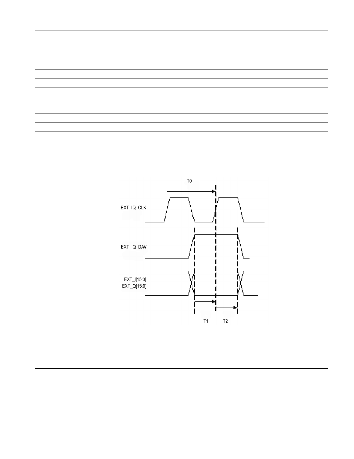
Table 55: EXT_IQ_DAV Duty cycle versus Span (cont.)
Span EXT_IQ_CLK frequency (MHz) EXT_IQ_DAV duty cycle (%)
50 kHz 50 0.19531
20 kHz 50 0.097656
10 kHz 50 0.048828
5 kHz 50 0.024414
2 kHz 50 0.006104
1 kHz 50 0.003052
500 kHz 50 0.001526
200 kHz 50 0.000763
100 kHz 50 0.000381
Specifications
The risi
ng edge of EXT_IQ_CLK is aligned to be in the center of the settled
EXT_I[15:0], EXT_Q[15:0], and EXT_IQ_DAV signals.
Figure 2: IQ Timing
able 56: IQ Timing
T
Real Time Span T0 T1 T2
>40MHz 6.6ns 1.54ns 1.58ns
≤40 MHz 20 ns 8.2 ns 8.4 ns
RSA5100A Series Technical Reference 45

Specifications
Possible Interruption
of Data from Digital I/Q
Outputs
There are three
data to the digital I/Q outputs. Those conditions are:
Alignments
Control Changes
Stitched Spectrum Mode
When any of these conditions are active, the EXT_IQ_DAV signal will be held in
its inactive state. The EXT_IQ_CLK signal will remain active and operate at the
frequency consistent with the SPAN value selected for the RSA5100A.
The EXT_IQ_DAV signal will remain inactive for the duration of any alignment
or control change. Once the alignment or control change has been completed, the
EXT_IQ_DAV signal becomes active again. While the EXT_IQ_DAV signal is
inactive, the data from the digital I/Q outputs are not valid and should be ignored.
The duty cycle of the EXT_IQ_DAV signal varies from 100% at the widest SPAN
values to a very small percentage at the narrowest SPAN
At a SPAN of 100 Hz, the duty cycle will be 0.00038%; here, the EXT_IQ_DAV
signal is active (high) for 20 ns, and then inactive (low) for ≈5.28 ms.
The length of time that the EXT_IQ_DAV signal is inactive can be used to
determine if the RSA5100A is performing an alignment or a control change. If
the EXT_IQ_DAV signal is inactive for longer than 10 ms, then the RSA5100A
digital I/Q output data stream has been interrupted.
conditions during which the RSA5100A will interrupt the fl ow of
values. (See Table 55.)
Digital IQ Output Scaling
External equipment used to detect the occurrence of a data interruption can
monitor the state of the EXT_IQ_DAV signal. If the EXT_IQ_DAV signal is
inactive for 10 ms or more, an alignment or control change has occurred. The
duration of the data interruption can be determined by measuring the time between
successive EXT_IQ_DAV pulses.
Output power in dBm for a sinusoidal input
Where:
Where:
I and Q are the digital values a t the Digital IQ output port
Ref = Reference Level
Valid for center frequencies that exceed:
Center frequency ≥ 80MHzforSpans>40MHz
Center frequency ≥ 30 MHz for Spans > 312.5 kHz and ≤ 40 MHz
Center frequency ≥ 2 MHz for Spans < 312.3 kHz
46 RSA5100A Series Technical Reference

Performance Verification
NOTE. The performance verification procedure is not a calibration procedure.
The performa
key specifications. For your instrument to be calibrated, it must be returned to a
Tektronix service facility.
nce verification procedure only verifies that your instrument meets
Prerequis
ites
The tests in this section make up an extensive, valid confirmation of p erformance
and functionality when the following requirements are met:
The cabinet must be installed on the instrument.
The instrument must have passed the Power On Self Tests (POST).
The instrument must have been last adjusted at an ambient temperature
between +18 °C (+64 °F) and +28 °C (+82 °F), must have been operating
for a warm-up period of at least 20 minutes after starting the RSA5100A
application, and must be operating at an ambient temperature. (See Table 50.)
Required Equipment
The procedures, use external, traceable signal sources to directly check warranted
acteristics. (See page 51, Warranted Characteristics Tests.) The following
char
table lists the equipment required for this procedure.
Table 57: Equipment required for Performance Verification
Item number and Minimum requirements Example Purpose
quency Range: 10 MHz; Accuracy: 1 x 10
1. Frequency Counter
2. RF Power Meter Agilent E4418B
3. RF Power Sensor 9 kHz to 18 GHz RF Flatness: <3% Calibration
4. Signal Generator Frequency Accuracy: ±3 x 10⁻⁷Output
Fre
actor data uncertainty: <2% (RSS)
f
Frequency: 0 to 20 GHz
–9
lent 53132A
Agi
Option 10
Agilent E9304A
Option H18
Anritsu MG3692B
Options 2A, 3A, 4, 15A,
16, 22, SM5821
Checking reference
output frequency
curacy
ac
Adjusting signal
nerator output level,
ge
checking reference
output power level
Checking RF flatness,
intermodulation
distortion, image
suppression, and
external reference
lock check.
RSA5100A Series Technical Reference 47

Performance Verification
Table 57: Equipment required for Performance Verification (cont.)
Item number and Minimum requirements Example Purpose
5. RF Signal
Generator
6. Precision
Attenuator
7. Network Analyzer
8. Power Splitter
9. Power Combiner Range: 0 to 14 GHz
10. Low Pass Filters
(2)
11. Voltmeter
12. BNC Cable 50 Ω, 36 in. male to male BNC connectors
13. N-N Cable 50 Ω, 36 in. male to male N connectors Signal interconnection
14. N-SMA Cable 50 Ω, 36 in. male N to male SMA connectors Signal interconnection
15. Termination,
Precision 50 Ω
16. N-Female to BNC
male Adapter
18. 3.5 mm (F) to
3.5 mm (F) coaxial
adapter
19. N-3.5mm cable
Output Frequency 0 to 18 GHz
Phase Noise at Center Frequency = 1 GHz
Offset
10 Hz
100 Hz
1kHz
10 kHz
100 kHz
1MHz
SSB Phase Noise (F) dBc/Hz
–71
–93
–118
–121
–119
–138
Anritsu MG3692B
Options 2A, 3A, 4, 15A,
16, 22, SM5821
Checking phase
noise and third
order intermodulation
distortion
30 dB
10 MHz to 3 GHz
10MHzto14GHz
Agilent 8757D with
directional bridge
1
Checking VSWR
Agilent 11667A Adjusting signal
generator output level
Isolation: >18 dB
Insertion loss: 6 dB
Agilent 11667A with
attenuators
2
Checking
intermodulation
distortion
3 dB = 2200 MHz
< 3 dB loss DC –3 GHz
>50 dB rejection 4 GHz to 14 GHz
Checking third order
intermodulation
distortion
Capable of measuring 30 VDC Standard Equipment Checking Noise Source
Tektronix part number
Signal interconnection
011-0049-01
Impedance: 50 Ω Type N m ale Signal interconnection
Tektronix part number
103-0058-00
N cable to RSA5100A
connections
Tektronix part number
131-8508-00
50 Ω, 36 in. male N to male SMA connectors
48 RSA5100A Series Technical Reference

Performance Verification
Table 57: Equipment required for Performance Verification (cont.)
Item number and Minimum requirements Example Purpose
20. N-Male to 3.5 mm
male adapter
21. 3.5 mm attenuator
1
The Agilent 85027A Directional Bridge can be used.
2
The Agilent 11667A Power Splitter can be used.
3 dB (two required)
Midwest Microwave
ATT-0550-03-35M-02
Checking third order
intermodulation
distortion
Preliminary Checks
These steps should be performed before proceeding to the Warranted
Charact
eristics tests.
Fan Check
Warm-up
Drive Check
CD
Touch Screen Check
Plug in the RSA5100A, power it on, and check that the fans located on the left
side of the RSA5100A are operating.
ON. Turn the RSA5100A off immediately if the fans are not operating.
CAUTI
Operating the Signal Analyzer without fans will damage the instrument.
sure the RSA5100A application is running, and allow the instrument to
Make
warm up for at least 20 minutes.
NOTE. The fans will slow down and be quieter when the application is started;
this is normal. Fan speed may vary while the application is running, depending
on the internal temperature detected by the instrument.
Press the button on the DVD-R/W drive (Option 57 only) and verify that the tray
door opens. Press the button again to close it.
Check that the touch screen detects touches:
1. Verify that the touch scre en is enabled (TouchScreenOffbutton is not
lighted).
2. Use your finger or a s tylus to touch several of the on-screen touchable
readouts, such as RBW or Span, and verify they become active when touched.
RSA5100A Series Technical Reference 49

Performance Verification
Diagnostics
Run a complete D
1. Select Tools > Diagnostics from the menubar.
2. Select the All Modules, All Tests checkbox at the top of the list.
3. Touch the RUN button. The diagnostics tests will take some time to complete,
and some of them are interactive:
a. Noise Source Drive 28VDC Out diagnostic will ask you to test the noise
source output on the RSA5100A rear-panel.
Check with a voltmeter that the voltage is 28 V ± 2 V.
b. The LED Check diagnostic will ask you to verify that all the highlighted
LEDs are turned on:
Compare the LEDs highlighted in the diagnostic display with the
Press each of the keys and rotate the knob on the front panel. You
Click the PASS or FAIL button when done.
c. The Display Pixel Test will ask you to look for video problems on the
test patterns:
iagnostics test session:
buttons on the front panel.
should see the corresponding key in the diagnostic display turn green.
Verify that each key is recognized.
Alignment
Check the Green screen for any stuck or missing pixels. Any keypress,
click, or touch will move to the next screen.
Repeat with the Red screen, the Blue Screen, and the Gray scale
screen. Select Yes or No when the LCD Test dialog asks “Did you
see any video problems”.
4. When all diagnostics tests have completed, check that there is a check mark
beside each diagnostic name. An X instead of a check mark indicates that
the diagnostic had a failure.
5. Click the Diagnostics Failure Info tab and verify there is no failure
information listed.
6. Click the Exit Diagnostics button to exit diagnostics.
You should align the instrument before proceeding with the Warranted
Characteristics tests.
1. Select Alignments in the To ol s menu. The Alignments dialog box will open.
2. Select Align Now. The alignment process will take a few minutes.
3. Verify that no alignment failures are reported in the status bar.
50 RSA5100A Series Technical Reference

Performance Verification
Warranted Cha
racteristics Tests
Frequency Accuracy
Check Reference Output
Frequency A
ccuracy
The following procedures verify the RSA5100A Series Signal Analyzer
performance is within the warranted specifications.
1. Connect Ref Out on the RSA5100A rear-panel through a 50 Ω precision
coaxial ca
2. Connect a precision frequency reference to the frequency counter.
ble to the frequency counter input. See the following figure.
Figure 3: Connections for Reference Frequency Output Accuracy check
3. Set the Frequency counter:
Function Frequency
Gate time
4. Check that the frequency counter reads 10 MHz ±4 Hz. Enter the frequency
in the test record.
2s
RSA5100A Series Technical Reference 51

Performance Verification
Check Reference Output
Power Level
1. Set up the power
NOTE. Store the power sensor correction factors in the power meter, if you have
not yet done so.
a. Connect the power sensor to the Sensor input on the power meter, as
shown in the following figure.
Figure 4: Power meter setup
b. Press Zero/Cal,thenpressZERO on the power meter.
c. Connect the RF input of the power sensor to the power meter power
reference output, as shown in the following figure.
meter and sensor.
Figure 5: Power meter calibration
d. Press CAL to execute the calibration.
e. Disconnect the RF input of the power sensor from the power meter
reference output.
2. Connect the power sensor RF input to the Ref Out connector on the
RSA5100A rear-panel, using the N-female to BNC male adapter (see the
following figure).
3. Press Frequency/Cal Factor, then set Freq to 10 MHz.
4. Check that the Ref Out signal is >0 dBm. Enter this level in the test record.
52 RSA5100A Series Technical Reference

Performance Verification
Figure 6: Equipment connections for Ref Out power level check
External Referenc e Input
Level
1. Connect the signal generator output to the Ref In connector on the RSA5100A
rear panel, using a 50 Ω N-N coaxial cable and N-female to BNC male adapter
(see the following figure).
Figure 7: Equipment connections for Ref In power level check
2. Set the Signal generator controls:
Frequency 10 MHz
Level 0 dBm
RF
On
3. Set the RSA5100A to use the external reference:
a. Select Setup > Confi gure In/Out > Frequency Reference.
b. Select the External radio button.
4. Check the Input Reference limits:
a. Check that the Status Bar shows Ref: Ext.
b. Set the Source to Internal (10 MHz).
c. Set the signal generator output level to –10 dBm.
RSA5100A Series Technical Reference 53

Performance Verification
d. Set the Source t
e. Check that the Status Bar shows Ref: Ext.
f. Set the Source to Internal (10 MHz ).
g. Set the signal generator output level to +6 dBm.
h. Set the Source to External.
i. Check that the Status Bar shows Ref: Ext.
j. Disconnec
message should pop up to indicate loss of lock (see the following figure).
Figure
8: Error message showing loss of lock to External Reference signal
o External.
t the signal generator from the Ref In connector. An error
k. Click
l. Ente
OK on the error message, and check that the Status Bar shows
Ref: Int.
r Pass or Fail in the test record.
Phase Noise (Instruments with Option 11)
ption 11 is installed in your instrument, use the following procedure to check
If O
the phase noise. If Option 11 is not installed in your instrument, use the procedure
(See page 56, Phase Noise (Instruments without Option 11).) that follows.
NOTE. The intent of the Phase Noise test is to measure the phase noise level of
the instrument. The phase noise specification does not cover residual spurs. If
the specific measurement frequency results in measuring a residual spur that
s visible above the noise level, the phase noise specification applies not to the
i
spur but to the noise level on either side of the spur. Please refer to the Spurious
Response specifications. (See Table 18.). Also, refer to the Spurious Response
section of this procedure to determine whether or not a residual spur is within
the specification. (See page 90, Spurious Response.)
54 RSA5100A Series Technical Reference

Performance Verification
1. Connect the gen
erator output to the RTSA RF Input, using a 50 Ω N-N coaxial
cable(seethefollowingfigure).
Figure 9: Equipment connections for phase noise checks
2. Reset the RSA5100A to factory defaults: select Setup > Preset (Main) from
the Setup menu.
3. Select Too ls > Alignments andthenselectAlign Now.
4. Modify the default settings:
Center Frequency
Setup > Settings > Freq & Span > Center
Span
Setup > Settings > Freq & Span > Span
Ref Level
Setup > Amplitude > Internal Settings > Ref Level
RF & IF Optimization
Setup > Amplitude > Internal Settings > RF & IF
Optimization
5. Set the generator as follows:
Center Frequency 1.00 GHz
Output level
RF
+5 dBm
On
6. Select Run > Run Single to stop acquisitions.
7. Display the Phase Noise measurement:
Select Setup > Displays.
Select the RF Measurements folder.
1.00 GHz
1MHz
+5 dBm
Maximize Dynamic Range
Select the Phase Noise display and select Add.
RSA5100A Series Technical Reference 55

Performance Verification
Select the Spec
Select OK.
8. Select Setup > Settings to display the Phase Noise settings control panel.
9. On the Frequency tab, set the Start Offset to 1 kHz for both the Measurement
BW and the Integration BW.
10. Set the Stop Offset to 10 MHz for both the Measurement BW and the
Integration BW.
11. Select the Parameters tab.
12. Set the Average value to 20 and click the check box to enable averaging.
13. Select the Traces tab.
14. Select T
so that Trace 2 is not be displayed.
15. Select
the Marker readout on the left side of the graph. Set the Marker value to
6MHz.
16. Press the Single key and wait for 20 averages to complete.
race 2 in the Trace drop-down list. Deselect the Show checkbox
Trace 1 from the trace drop-down list above the graph display. Select
trum display and select Remove.
17. Read t
18. Document the test results in the test record at each frequency.
he value for the 6 MHz offset from the Offset readout.
Phase Noise (Instruments without Option 11)
Check Phase Noise
If Option 11 is not installed in your instrument, use the following procedure
check the phase noise. If Option 11 is installed in your instrument, use the
to
preceding (See page 54, Phase Noise (Instruments with Option 11).) procedure.
NOTE. The intent of the Phase Noise test is to measure the phase noise level of
the instrument. The phase noise specification does not cover residual spurs. If
the specific measurement frequency results in measuring a residual spur that
is visible above the noise level, the phase noise specification applies not to the
spur but to the noise level on either side of the spur. Please refer to the Spurious
Response specifications. (See Table 18.). Also, refer to the Spurious Response
section of this procedure to determine whether or not a residual spur is within
the specification. (See page 90, Spurious Response.)
56 RSA5100A Series Technical Reference

Performance Verification
1. Connect the gen
erator output to the RTSA RF Input, using a 50 Ω N-N coaxial
cable(seethefollowingfigure).
Figure 10: Equipment connections for phase noise checks
2. Reset the RSA5100A to factory defaults: Select Setup > Preset (Main) from
the Setup menu.
3. Press Tools > Alignments and then select Align Now.
4. Modify the settings:
Center Frequency
Setup > Settings > Freq & Span > Center
Span
Setup > Settings > Freq & Span > Span
VBW
Setup > Settings > BW > VBW
Detection
Setup > Settings > Traces > Detection
Function
Setup > Settings > Traces > Function
Count
Setup > Settings > Traces > Count
Trace Points
Setup > Settings > Prefs > Trace Points
Marker Noise Mode
Setup > Settings > Prefs > Marker Noise Mode
RF & IF Optimization
Setup > Amplitude > Internal Settings > RF & IF
Optimization
Reference level
Setup > Amplitude > Internal Settings > Ref Level
1.00 GHz
1MHz
10 Hz (box checked)
Avg (VRMS)
Avg (VRMS)
100 (box checked)
2401
Check Marker Noise mode box
Maximize Dynamic Range
+5 dBm
RSA5100A Series Technical Reference 57

Performance Verification
5. Set the generat
Frequency
Output level
RF
or as follows:
1.00 GHz
+5 dBm
On
6. Turn on the Reference Marker (MR) and Marker 1 (M1), and set them for
Delta opera
tion and Noise Mode.
a. Select Markers > Define Markers.
b. Select the Add soft key to add the MR marker.
c. Select the Add soft key again to add the M1 marker.
d. Select Delta from the Readouts dropdown menu.
7. For each span shown in the following table, perform steps through :
Table 58: Phase noise offsets (Low range; without Option 11)
Span M1 Offset
4kHz
40 kHz
300 kHz
CF + 1 kHz
CF + 10 kHz
CF + 100 kHz
a. Press the Span key and enter a Span value from the table.
b. Select Run > Run Single.
c. Select the Reference Marker with the Marker Select key and press the
Peak key.
d. Select Marker 1 (M1) with the marker select key.
e. Set the Marker 1 (M1) frequency by entering the offset value from the
table above in the Frequency box at the bottom center of the display.
f. Read the marker noise level in dBc/Hz, in the Delta Marker readout
(upper right corner of the s creen), and enter the value in the test record.
(Limits are shown in the test record.)
8. Record the generator signal amplitude in the Test Record:
a. Select Marker (MR) with the Marker Select key.
b. Select the Markers Peak key to center the MR marker on the peak of the
1000 MHz signal.
c. Record the MR Marker amplitude (upper-left corner of the screen.) This
value is called Carrier Power andisusedbelow.
58 RSA5100A Series Technical Reference

Performance Verification
9. Obtain the phas
settings listed below:
a. Center Frequency (Freq key): 1001 MHz
b. Span (Span key): 10 kHz
c. Reference Level Offset: -30 dBm (This is the amplitude control in the
upper left of the display.)
d. Set input attenuation for manual control.
Select Setup > Amplitude > Internal Settings .
Deselect the Internal Attenuator Auto check box.
Set Internal Attenuator to 0 dB.
a. Select Run > Run Single.
b. Center the M1 marker in the middle of the screen:
Select Markers > Define Markers
Select Readouts > Absolute.
Press the Select key to select the M1 mar
Select Marker Frequency. Set to 1001 MHz.
e noise at 1 MHz offset. Start by setting the RSA5100A to the
ker.
The marker is now located at the center frequency position.
a. Read the noise amplitude on Marker M1,indBm/Hz.
b. Subtract the value of MR obtained in step 8 to obtain the phase noise
amplitude at 1 MHz.
For example, if MR = 4.7 dBm and M1 = –129.6 dBm/Hz, then M1-MR =
–134.3 dBc/Hz.
c. Enter the value obtained at 1 MHz in the test record for phase noise at
1MHz.
10. Obtain the phase noise at 6 MHz offset. Start by setting the RSA5100A to the
settings listed below:
a. Center Frequency (Freq key): 1006 MHz.
b. Span (Span key): 10 kHz.
c. Select Run > Run Single.
d. Set the Mar
e. Read the noise level on Marker M1 in dBm/Hz.
f. Subtract the value of Carrier Power obtained in step 8 in order to obtain
the phase noise amplitude at +6 MHz.
kerM1Frequencyto1006MHz..
RSA5100A Series Technical Reference 59

Performance Verification
For example, if
M1-Carrier Power = – 49.8 dBc/Hz.
g. Enter the valu
6MHz.
11. Obtain the p
to the settings below:
a. Center Freq
b. Span (Span key): 10 kHz.
c. Select Run > Run Single.
d. Set the Marker Frequency to 1010 MHz.
NOTE. The intent of the Phase Noise test is to measure the phase noise level of
the instrument. The phase noise specification does not cover residual spurs. If
the spe
is visible above the noise level, the phase noise specification applies not to
the spur but to the noise level on either side of the spur. Please refer to the
Spurious Response specifications. (See Table 18.). Also, refer to the Spurious
Response section of this procedure to determine whether or not a residual spur
is within the specification. (See page 90, Spurious Response.)
hase noise at 10 MHz offset. Start by setting the RSA5100A
cific measurement frequency results in measuring a residual spur that
Carrier Power = 4.7 dBm and M1 = -145.1 dBm/Hz, then
e obtained at 6 MHz in the test record for phase noise at
uency (Center key): 1010 MHz.
e. Read the noise amplitude on marker M1 in dBm/Hz.
f. Subtract the value of the Carrier Power marker obtained in step 8 to obtain
the phase noise amplitude at +10 MHz.
For example, if Carrier Power = 4.7 dBm and M1 = –146.1 dBm/Hz,
Then M1-Carrier Power = –150.8 dBc/Hz.
g. Enter the value obtained at 10 MHz in the test record for phase noise
at 10 MHz.
60 RSA5100A Series Technical Reference

RF Input
Performance Verification
Input VSWR (Preamp OFF)
1. Connect the RSA5100A and the Network Analyzer as shown in the following
figure.
NOTE. Verify that the network analyzer is properly calibrated, as specified by the
manufacturer, before taking measurements on the RSA5100A.
Figure 11: Equipment connections for VSWR check
2. Reset the RSA5100A to factory defaults: select Setup > Preset (Main).
3. Select Setup > Amplitude > Internal Settings. Desele ct the Auto check box
and set the Internal Attenuator valueto10dB.
4. Set up the Network Analyzer as follows:
a. Pres
b. Calibration > Cal Set > [select appropriate Cal Set] > OK.
c. Trace>Format>SWR>OK
d. Scale > Scale > Per Division > 100 mUnits > OK.
e. Set Span (F4) to 100 MHz.
5. Set the Center frequency of the RSA5100A to each frequency in the
RSA5103A/RSA5106A VSWR test frequencies table. Set the Network
Analyzer center frequency [Start/Center > Center (F3)] to the same frequency.
Press Marker Search > MAX (F1) and record the value in the table.
6. Enter the highest VSWR in the table in the test record.
7. RSA5106A only: Set the Center frequency of the RSA5100A to each
frequency in the RSA5106A VSWR test frequencies table. Set the Network
et.
RSA5100A Series Technical Reference 61

Performance Verification
Analyzer cente
r frequency [Start/Center > Center (F3)] to the same frequency.
Press Marker Search > MAX (F1) and record the value in the table.
8. RSA5106A only: Enter the highest VSWR in the table in the test record.
Table 59: RSA5103A VSWR Test Frequencies (MHz)
60 560 1060 1560 2060 2560
160 660 1160 1660 2160 2660
260 760 1260 1760 2260 2760
360 860 1360 1860 2360 2860
460 960 1460 1960 2460 2960
Table 60: RSA5106A VSWR Test Frequencies (GHz)
3.05 3.55 4.05 4.55 5.05
3.15 3.65 4.15 4.65 5.15 5.65 6.15
3.25 3.75 4.25 4.75 5.25
3.35 3.85 4.35 4.85 5.35 5.85
3.45 3.95 4.45 4.95 5.45 5.95
Input VSWR (Preamp ON -
Option 50 Only)
1. Reset the RSA5100A to factory defaults: select Setup > Preset (Main).
2. Select Setup > Amplitude > Internal Settings. Deselect the Auto check box
5.55
5.75
6.05
and set the Internal Attenuator to 10 dB.
3. Select Setup > Amplitude > Internal Settings. Select the Internal Preamp
check box.
4. Set up the Network Analyzer as follows:
Preset.
Calibration > Cal Set > [select appropriate Cal set ] > OK.
Trace > Format > SWR > OK.
Scale > Scale > Per Division > 100 mUnits > OK.
Set Span (F4) to 100 MHz.
5. Set the Center frequency of the RSA5100A to each frequency in the
RSA5100A VSWR Preamp On Test Frequencies table. Set the Network
Analyzer center frequency (Start /Center > Center (F3)) to the same frequency.
Press Marker Search > MAX (F1) and record the value in the table.
Table 61: RSA5100A VSWR Preamp On Test Frequencies (MHz)
60 560 1060 1560 2060 2560
160 660 1160 1660 2160 2660
62 RSA5100A Series Technical Reference

Performance Verification
Table 61: RSA5100A VSWR Preamp On Test Frequencies (MHz) (cont.)
260 760 1260 1760 2260 2760
360 860 1360 1860 2360 2860
460 960 1460 1960 2460 2960
6. Enter the h
ighest VSWR in the table in the test record.
7. RSA5106A only: Set the Center frequency of the RSA5106A to each
frequenc
y in the RSA5106A VSWR Preamp On Test Frequencies table. Set
the Network Analyzer center frequency (Start /Center > Center (F3)) to the
same frequency. Press Marker Search > MAX (F1) and record the value in
the table.
Table 62: RSA5106A VSWR Preamp On Test Frequencies (GHz)
3.05 3.55 4.05 4.55 5.05
3.15 3.65 4.15 4.65 5.15 5.65 6.15
3.25 3.75 4.25 4.75 5.25
3.35 3.85 4.35 4.85 5.35 5.85
3.45 3.95 4.45 4.95 5.45 5.95
5.55
5.75
6.05
8. RSA5106A: Enter the highest VSWR in the table in the test record.
RSA5100A Series Technical Reference 63
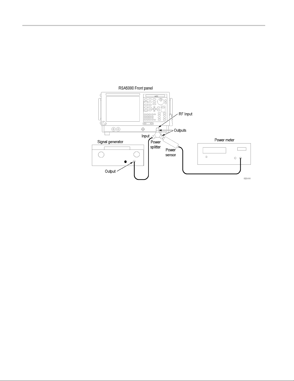
Performance Verification
Amplitude
RF Flatness (Frequ ency
Response) 10 MHz to
6.2 GHz
1. Connect the RF generator, power splitter, power meter, and RSA5100A, as
shown in the following figure.
The power splitter outputs should connect directly to the RSA5100A RF Input
and to the Power Sensor, without using cables.
Figure 12: Equipment connections for RF Flatness check
2. To record the test readings, you can make a printout of the following table.
(See Table 63.)
3. Reset the RSA5100A to factory defaults: Setup > Preset (Main).
4. Select To o ls > Alignments and then select Align Now.
5. Set the RSA5100A as follows:
Level
Ref
Setup > Amplitude >Internal Settings > Ref Level
ternal Attenuator
In
Setup > Amplitude > Internal Settings > Internal
Attenuator
Span
etup > Settings > Freq & Span> Span
S
LF Path
etup > Acquire > Input Params
S
–15 dBm
10dB (Auto unchecked)
1MHz
Use Low Freq... box unchecked
6. Set the RF signal generator for a -14 dBm output amplitude and turn RF On..
64 RSA5100A Series Technical Reference

Performance Verification
7. Set both the RF s
ignal generator output frequency and the RSA5100A Center
Frequency to the first frequency in the RF Flatness table that follows. This is
the reference frequency. (See Table 63.)
8. Select the Markers Peak key to set the Reference Marker (MR) to the carrier
peak.
9. Adjust the RF signal generator output level for a marker reading of –20
±0.5dBm.
10. Record the Power Meter reading and the RSA5100A marker reading in the
following table.
11. Set both the RF Generator output frequency and the RSA5100A center
frequency to the next frequency in the table.
12. Press the Markers Peak key to set the Reference Marker (MR) to the carrier
peak.
13. Calculate the ΔPower Meter number: subtract the Power meter reading at
100 MHz from the Power Meter reading at this frequency.
14. Calculate the ΔRTSA number: subtract the RTSA reading at 100 MHz from
the RTSA reading at this frequency.
15. Calculate the RF Flatness Error:
RF Flatness Error = ΔRTSA at this freq – ΔPower Meter at this freq
Readings are in dBm, error is in dB.
16. Repeat items 11 through 15 for each of the center frequencies shown in the
RF Flatness table. (See Table 63.)
Table 63: RF Flatness (Preamp OFF)
Attenuator = 10 dB
Power meter
Frequency
100 MHz 0 0 0
10 MHz
20 MHz
30 MHz
40 MHz
50 MHz
60 MHz
70 MHz
80 MHz
90 MHz
200 MHz
reading
∆ Power meter
(vs. 100 MHz) RTSA reading
∆ RTSA reading
(vs. 100 MHz)
RF flatness
1
error
RSA5100A Series Technical Reference 65

Performance Verification
Table 63: RF Flatness (Preamp OFF) (cont.)
Attenuator = 10 dB
Frequency
300 MHz
400 MHz
500 MHz
600 MHz
700 MHz
800 MHz
900 MHz
1.0 GHz
1.1 GHz
1.2 GHz
1.3 GHz
1.4 GHz
1.5 GHz
1.6 GHz
1.7 GHz
1.8 GHz
1.9 GHz
2.0 GHz
2.1 GHz
2.2 GHz
2.3 GHz
2.4 GHz
2.5 GHz
2.6 GHz
2.7 GHz
2.8 GHz
2.9 GHz
3.0 GHz
RSA5106A only
3.1 GHz
3.2 GHz
3.3 GHz
3.4 GHz
3.5 GHz
3.6 GHz
Power meter
reading
∆ Power meter
(vs. 100 MHz) RTSA reading
∆ RTSA reading
(vs. 100 MHz)
RF flatness
1
error
66 RSA5100A Series Technical Reference

Table 63: RF Flatness (Preamp OFF) (cont.)
Attenuator = 10 dB
Frequency
3.7 GHz
3.8 GHz
3.9 GHz
4.0 GHz
4.1 GHz
4.2 GHz
4.3 GHz
4.4 GHz
4.5 GHz
4.6 GHz
4.7 GHz
4.8 GHz
4.9 GHz
5.0 GHz
5.1 GHz
5.2 GHz
5.3 GHz
5.4 GHz
5.5 GHz
5.6 GHz
5.7 GHz
5.8 GHz
5.9 GHz
6.0 GHz
6.1 GHz
6.2 GHz
1
UsetheformulainStep15
Power meter
reading
∆ Power meter
(vs. 100 MHz) RTSA reading
∆ RTSA reading
(vs. 100 MHz)
Performance Verification
RF flatness
1
error
17. Enter the largest variation in each of the following frequency ranges into the
test record:
10 MHz - 3 GHz (Preamp OFF)
3 GHz - 6.2 GHz (Preamp Off, RSA5106A only)
RSA5100A Series Technical Reference 67
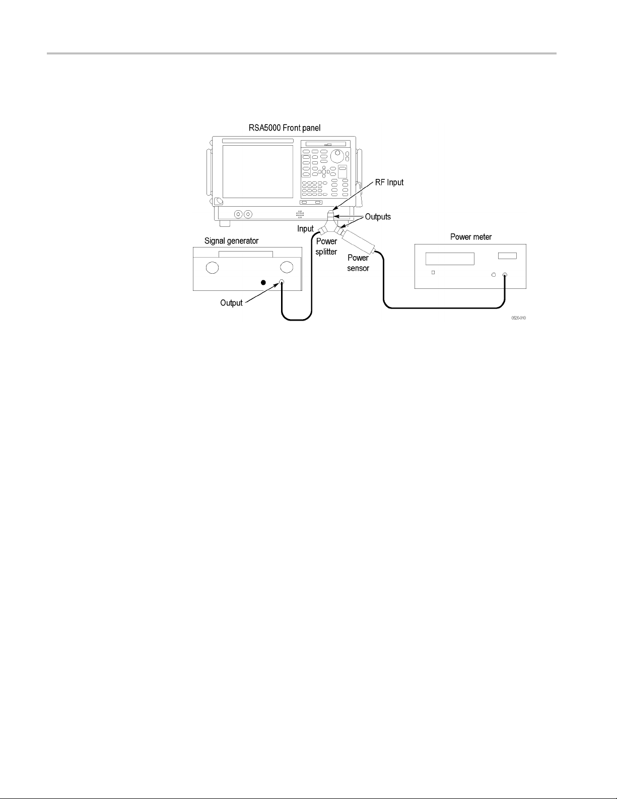
Performance Verification
Low Frequency (LF) Input
Path Accuracy
1. Connect the RF g
enerator, power splitter, power meter, and RSA5100A, as
shown in the following figure.
Figure 13: Equipment connections for Low Frequency (LF) input path accuracy
check
2. The power splitter outputs should connect directly to the RSA5100A RF Input
and to t
he Power Sensor, without using cables.
3. Reset the RSA5100A to factory defaults; select Setup > Preset (Main).
4. Select To o ls > Alignments and then select Align Now.
5. Set the RSA5100A as follows:
Ref Level
Setup > Amplitude > Internal Settings > Ref
Level
Internal Attenuator
Setup > Amplitude > Internal Settings
Span
Setup > Settings > Freq & Span > Span
LF Path
Setup > Acquire > Input Params
–15 dBm
10 dB (Auto unchecked)
1MHz
Use Low Freq box checked
6. Set the RF generator for a –14 dBm output amplitude and turn RF On.
7. Set both the RF signal generator output frequency and the RSA5100A Center
Frequency to the first frequency shown in the table Low Frequency Input
Path Flatness (Preamp Off, if installed) (See Table 64.). This is the reference
frequency.
68 RSA5100A Series Technical Reference

Performance Verification
8. Select the Mark
ers Peak key to set the Reference Marker (MR) to the carrier
peak.
9. Adjust the RF signal generator output level for a maker reading of
–20 ± 0.5 dBm.
10. Record the Power Meter reading and the RSA5100A marker reading in the
following table.
11. Set both the RF generator output frequency and the RSA5100A Center
Frequency to the next frequency in the table.
12. Select the Markers Peak key to set the Reference Marker (MR) to the carrier
peak.
13. Record the Power Meter reading and the RSA5100A marker reading in the
following table.
14. Calculate the Δ Power Meter number: subtract the Power Meter reading at
10 MHz from the Power Meter reading at this frequency.
15. Calculate the Δ RTSA number: subtract the RTSA reading at 10 MHz from
the RTSA reading at this frequency.
16. Calculate the RF Flatness Error:
RF Flatness Error = Δ RTSA at this freq - Δ Power Meter at this freq
Readings are in dBm, error is in dB.
17. Repeat parts 11 through 16 for each of the center frequencies shown in the
following table.
Table 64: Low Frequency Input Path Flatness (Preamp OFF)
Attenuator = 10 dB
Power meter
Frequency
10 MHz 0 0 0
11 M Hz
12 MHz
13 MHz
14 MHz
15 MHz
16 MHz
17 MHz
18 MHz
19 MHz
20 MHz
21 M Hz
reading
∆ Power meter
(vs. 10 MHz) RTSA reading
∆ RTSA reading
(vs. 10 MHz)
RF flatness
1
error
RSA5100A Series Technical Reference 69

Performance Verification
Table 64: Low Frequency Input Path Flatness (Preamp OFF) (cont.)
Attenuator = 10 dB
Frequency
22 MHz
23 MHz
24 MHz
25 MHz
26 MHz
27 MHz
28 MHz
29 MHz
30 MHz
31 MHz
31.49 MHz
1
e formula in Step 16
Use th
Power meter
reading
∆ Power meter
(vs. 10 MHz) RTSA reading
∆ RTSA reading
(vs. 10 MHz)
RF flatness
1
error
18. Enter the largest variation in each of the following frequency range into the
ecord:
test r
10 MHz - 32 MHz (Preamp OFF)
70 RSA5100A Series Technical Reference
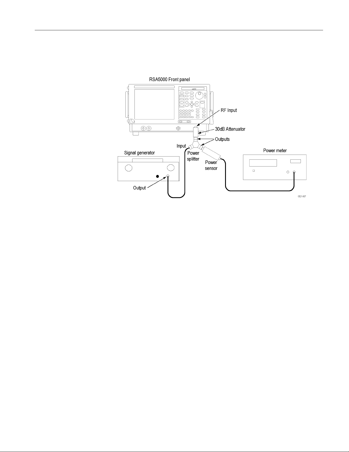
Performance Verification
RF Flatness (Frequency
Response) 10 MHz to
6.2 GHz , Preamp On
(Option 50 Installed )
1. Connect the RF g
enerator, power splitter, power meter, and RSA5100A, as
shown in the following figure. The 30 dB attenuator is connected between the
power splitter and the RSA5100A RF input connector.
Figure 14: Equipment connections for RF Flatness (Frequency Response) 10 MHz
to 6.2 GHz check
2. Reset the RSA5100A to factory defaults: select Setup > Preset (Main).
3. Select Too ls > Alignments andthenselectAli
gn Now.
4. Set the RSA5100A as follows:
Ref Level
Setup > Amplitude > Internal Settings > Ref
Level
Internal Attenuator
Setup > Amplitude > Internal Attenuator
Internal Preamp
Setup > Amplitude > Internal Settings
Span
Setup > Settings > Freq & Span > Span
LF Path
Setup > Acquire > Input P arams
–45 dBm
10 dB (Auto unchecked)
Internal Preamp box checked
1MHz
Use Low Freq Signal path box unchecked
5. Set the RF generator for a –14 dBm output amplitude and turn RF On.
6. Set both the RF signal generator output frequency and the RSA5100A Center
Frequency to the first frequency shown in the table RF Flatness (Option 50
Preamp ON) (See Table 65.). This is the reference frequency.
RSA5100A Series Technical Reference 71

Performance Verification
7. Select the Mark
ers Peak key to set the Reference Marker (MR) to the carrier
peak.
8. Record the Power Meter reading and the RSA5100A marker reading in the
following table.
9. Set both the RF generator output frequency and the RSA5100A Center
Frequency to the next frequency in the table.
10. Select the Markers Peak key to set the Reference Marker (MR) to the carrier
peak.
11. Calculate the ΔPower Meter number: subtract the Power Meter reading at
100 MHz from the Power Meter reading at this frequency.
12. Calculate the ΔRTSA number: subtract the RTSA reading at 100 MHz from
the RTSA reading at this frequency.
13. Calculate the RF Flatness Error:
RF Flatness Error = ΔRTSA at this freq - ΔPower Meter at this freq + delta
30 dB attenuator at this frequency
Readings are in dBm and error is in dB.
14. Repeat steps 9 through 13 for each of the center frequencies shown in the
following table.
Table 65: RF Flatness (Option 50 Preamp ON)
Attenuator = 10 dB
Power
meter
Frequency
100 MHz 0 0 0 0
10 MHz
20 MHz
30 MHz
40 MHz
50 MHz
60 MHz
70 MHz
80 MHz
90 MHz
200 MHz
300 MHz
400 MHz
500 MHz
600 MHz
reading
∆ Power
meter (vs.
100 MHz)
RTSA
reading
∆ RTSA
reading (vs.
100 MHz)
30 dB
attenuator
Δ30 dB
attentuator
RF flatness
1
error
72 RSA5100A Series Technical Reference

Table 65: RF Flatness (Option 50 Preamp ON) (cont.)
Attenuator = 10 dB
Frequency
700 MHz
800 MHz
900 MHz
1.0 GHz
1.1 GHz
1.2 GHz
1.3 GHz
1.4 GHz
1.5 GHz
1.6 GHz
1.7 GHz
1.8 GHz
1.9 GHz
2.0 GHz
2.1 GHz
2.2 GHz
2.3 GHz
2.4 GHz
2.5 GHz
2.6 GHz
2.7 GHz
2.8 GHz
2.9 GHz
3.0 GHz
RSA5106A only
3.1 GHz
3.2 GHz
3.3 GHz
3.4 GHz
3.5 GHz
3.6 GHz
3.7 GHz
3.8 GHz
3.9 GHz
Power
meter
reading
∆ Power
meter (vs.
100 MHz)
RTSA
reading
∆ RTSA
reading (vs.
100 MHz)
30 dB
attenuator
Performance Verification
Δ30 dB
attentuator
RF flatness
error
1
RSA5100A Series Technical Reference 73

Performance Verification
Table 65: RF Flatness (Option 50 Preamp ON) (cont.)
Attenuator = 10 dB
Power
meter
Frequency
4.0 GHz
4.1 GHz
4.2 GHz
4.3 GHz
4.4 GHz
4.5 GHz
4.6 GHz
4.7 GHz
4.8 GHz
4.9 GHz
5.0 GHz
5.1 GHz
5.2 GHz
5.3 GHz
5.4 GHz
5.5 GHz
5.6 GHz
5.7 GHz
5.8 GHz
5.9 GHz
6.0 GHz
6.1 GHz
6.2 GHz
1
UsetheformulainStep13
reading
∆ Power
meter (vs.
100 MHz)
RTSA
reading
∆ RTSA
reading (vs.
100 MHz)
30 dB
attenuator
Δ30 dB
attentuator
RF flatness
1
error
15. Enter the largest variation in each of the following frequency range into the
test record:
10 MHz - 3 GHz (Preamp On, Option 50 only)
3.1 MHz - 6.2 GHz (Preamp On, RSA5106A only)
74 RSA5100A Series Technical Reference

Performance Verification
Low Frequency (LF) Input
Path, Preamplifier On
Accuracy (Option 50 Only)
1. Connect the RF g
enerator, power splitter, power meter, and RSA5100A, as
shown in the following figure.
Figure 15: Equipment connections for Low Frequency (LF) input path accuracy
check
NOTE. The power splitter outputs should connect directly to the RSA5100A RF
Input and to the Power Sensor, without using cables. The 30 dB attenuator is
connected between the power splitter and the RSA5100A RF input connector.
2. Reset the RSA5100A to factory defaults: select Setup > Preset (Main).
3. Select Too ls > Alignments and select Align Now.
4. Set the RSA5100A as follows:
Ref Level
Setup > Amplitude > Internal Settings > Ref Level
Internal Attenuator
Setup > Amplitude > Internal Attenuator
Internal Preamp
Setup > Amplitude > Internal Settings
Span
Setup > Settings > Freq & Span > Span
LF Path
Setup > Acquire > Input Params
–45 dBm
10 dB (Auto unchecked)
Internal Preamp box
checked
1MHz
Use Low Freq Signal
path box checked
5. Set the RF generator for a –14 dBm output amplitude and turn RF On.
RSA5100A Series Technical Reference 75

Performance Verification
6. Set both the RF s
ignal generator output frequency and the RSA5100A Center
Frequency to the first frequency shown in the table Low Frequency Input Path
Flatness (Preamp ON) (See Table 66.). This is the reference frequency.
7. Select the Markers Peak key to set the Reference Marker (MR) to the carrier
peak.
8. Adjust the RF signal generator level for a marker reading of –50 ±0.5 dBm
9. Record the Power Meter reading and the RSA5100A marker reading in the
following table. (See Table 66.)
10. Set both the RF generator output frequency and the RSA5100A Center
Frequency to the next frequency in the table. (See Table 66.)
11. Select the Markers Peak key to set the Reference Marker (MR) to the carrier
peak.
12. Record the Power Meter reading and the RSA5100A marker reading in the
following table. (See Table 66.)
13. Calculate the ΔPower Meter number: subtract the Power Meter reading at
10 MHz from the Power Meter reading at this frequency.
14. Calculate the ΔRTSA number: subtract the RTSA reading at 10 MHz from
the RTSA reading at this frequency.
15. Calculate the RF Flatness Error:
RF Flatness Error = ΔRTSA at this freq - ΔPower Meter at this frequency +
delta 30 dB attenuator at this frequency
Readings are in dBm and error is in dB.
16. Repeat steps 10 through 15 for each of the center frequencies shown in the
following table.
Table 66: Low Frequency Input Path Flatness (Preamp ON)
Attenuator = 10 dB
Power
meter
Frequency
10 MHz 0 0 0
11 MHz
12 MHz
13 MHz
14 MHz
15 MHz
16 MHz
17 MHz
reading
∆ Power
meter (vs.
10 MHz)
RTSA
reading
∆ RTSA
reading (vs.
10 MHz)
30 dB
attenuator
Δ30 dB
attenuator
RF flatness
1
error
76 RSA5100A Series Technical Reference

Table 66: Low Frequency Input Path Flatness (Preamp ON) (cont.)
Attenuator = 10 dB
Power
meter
Frequency
18 MHz
19 MHz
20 MHz
21 MHz
22 MHz
23 MHz
24 MHz
25 MHz
26 MHz
27 MHz
28 MHz
29 MHz
30 MHz
31 MHz
31.49 MHz
1
UsetheformulainStep15
reading
∆ Power
meter (vs.
10 MHz)
RTSA
reading
∆ RTSA
reading (vs.
10 MHz)
30 dB
attenuator
Performance Verification
Δ30 dB
attenuator
RF flatness
error
1
Absolute Accuracy at
Calibration Point, RF Path
17. Enter the largest variation in each of the following frequency range into the
test record:
10MHz-32MHz(PreampON)
1. Connect the RF generator, power splitter, power meter, and RSA5100A.
(See Figure 12.)
2. Reset the RSA5100A to factory defaults: select Setup > Preset (Main).
elect Too ls > Alignments and select Align Now.
3.S
4. Set the RSA5100A:
Reference Level
Setup > Amplitude > Internal Settings > Ref Level
Center Frequency
Setup > Settings > Center
–20 dBm
100 MHz
5. Set the RF Generator:
RSA5100A Series Technical Reference 77

Performance Verification
Absolute Accuracy at
Calibration Point, LF path
Output Frequency
Output Level
RF
100 MHz
–14 dBm
On
6. Set the frequency span (Span key) to 300 kHz.
7. Press the Markers > Peak key to set the Reference Marker (MR) to the
carrier peak.
8. Record the reading on the Power Meter and on the RSA5100A marker
amplitude.
9. Calculate the Absolute Amplitude Accuracy:
Delta = RSA5100A reading - Power Meter reading
Readings are in dBm, error is in dB.
10. Record the Absolute Amplitude Error in t he test record. (Limits are shown in
the test record.)
11. Repeat steps 6 through 10 for frequency spans of 1MHz and 25.1MHz
(Option40or85).
1. Connect the RF generator, power splitter, power meter, and RSA5100A.
(See Figure 12.)
2. Reset the RSA5100A to factory defaults: select Setup > Preset (Main).
3. Select To o ls > Alignments and select Align Now.
4. Set the RSA5100A:
Reference Level
Setup > Amplitude > Internal Settings > Ref Level
Center Frequency
Setup > Settings > Center
Span
Setup > Settings > Freq & Span > Span
LF Path
Setup > Acquire > Input Params
–20 dBm
10 MHz
1MHz
Use Low Freq signal path checked
5. Set the RF Generator:
Output Frequency
Output Level
RF
10 MHz
–14 dBm
On
6. Press the Markers Peak key to set the Reference Marker (MR) to the carrier
peak.
78 RSA5100A Series Technical Reference

Performance Verification
Noise and D
istortion
Third Order
Intermodulation Distortion
7. Record the read
amplitude.
8. Calculate the
Delta = RSA5100A reading - Power Meter reading
Readings are in dBm, error is in dB.
9. Record the Absolute Amplitude Error in the test record. (Limits are shown in
the test record.)
1. Set up the RF sinewave generators, Lowpass filters, Signal Combiner, and
RSA5100A as shown in the following figure.
ingonthePowerMeterandontheRSA5100Amarker
Absolute Amplitude Accuracy:
Figure 16: Equipment connections for Third Order Intermodulation Distortion check
2. Reset the RSA5100A to factory defaults: select Setup > Preset (Main).
3. Select Too ls > Alignments and select Align Now.
4. Set the RSA5100A:
Ref Level
Setup > Amplitude > Internal Settings > Ref Level
Internal Attenuator
Setup > Amplitude > Internal Settings > Internal
Attenuator
RSA5100A Series Technical Reference 79
–20 dBm
0 dB (Auto unchecked)

Performance Verification
RF & IF Optimization
Setup > Amplitude > Internal Settings > RF & IF
Optimization
Span
Setup > Settings > Freq & Span > Span
RBW
Setup > Settings > BW > RBW
Function
Setup > Settings > Traces > Function
Averaging
(Settings >Traces > Avg (VRMS)
Maximize Dyna
10 kHz
Auto checke
Avg (VRMS)
25 (Count checked)
mic Range
d
5. Set each of the rf signal generators to provide a power level of – 22 dBm
andturnRFOn.
a. Set the first generator output frequency to 2.1295 GHz, and the second
generator output frequency to 2.1305 GHz.
b. Set the RSA5100A Function to Normal (Setup > Settings > Traces >
Function > Normal).
c. Set the RSA5100A Center frequency to 2.1295 GHz. Press the Markers
Peak key. Adjust the first generator output level for a marker reading of
–25.0dBm. Record this as carrier #1.
d. Set the RSA5100A Center frequency to 2.1305 GHz Press the Markers
Peak key. Adjust the second generator output level for a marker reading
25.0. This is carrier amplitude #2.
of –
6. Set the RSA5100A Function to Averaging (Setup > Settings > Traces >
ction>Avg(VRMS)).
Fun
7. Set the RTSA center frequency to 2.1285 GHz. After averaging has
mpleted, press the Markers Peak key and read the amplitude level of the
co
signal displayed at the center of the screen. Record this as TOI #1.
et the RTSA center frequency to 2.1315 GHz. After averaging has
8.S
completed, press the Markers > Peak key and read the amplitude level of the
signal displayed at the center of the screen. Record this as TOI #2.
9. Calculate the Third Order Intermodulation Distortion (TOI) using the
following procedure. Record the results in the test record.
a. Record the maximum reading from step 7 or step 8.
b. Record the minimum reading from step 5 c or step 5 d.
c. Calculate the TOI using this equation:
TOI = step a – step b
80 RSA5100A Series Technical Reference

Performance Verification
DANL - P reamp OFF, LF
Path
1. Terminat e the R
SA5100A RF Input with a 50 Ω terminator.
2. Reset the RSA5100A to factory defaults: select Setup > Preset (Main).
3. Select Too ls > Alignments and select Align Now.
4. Set the RSA5100A:
Reference Level
Setup > Amplitude > Ref Level
Internal Attenuator
Setup > Amplitude > Internal Attenuator
RF & IF Optimization
Setup > Amplitude > RF & IF Optimization
Center Frequency
Setup > Settings > Freq & Span > Center
Span
Setup > Settings > Freq & span > Span
RBW
Setup > Settings > BW > RBW
Detection
Setup > Settings > Traces > Detection
Function
Setup > Settings > Traces > Function
Count
Setup > Settings > Traces > Function
LF Path
Setup > Acquire > Input Params
–50 dBm
0 dB (Auto unchecked)
Minimize Noise
9kHz
1kHz
Auto (box checked)
Avg ( of logs)
Avg ( of logs)
100 ( Count box checked)
Use Low Freq... box checked
5. Set
the markers for Noise Mode operation:
a. Select Markers > Define Markers.
b. Select the Add soft key to add the Reference marker (MR).
c. Select Add againtoaddtheM1marker.
d. Select Absolute from the Readouts drop-down list.
e. Select Setup > Settings ,clickthePrefs tab, and then select the Marker
Noise Mode checkbox so it is checked.
6. Set the RSA5100A to each of the Center Frequencies listed in the following
table by pressing the Freq key and entering the value listed.After averaging is
RSA5100A Series Technical Reference 81

Performance Verification
completed, pre
ss the Markers > Peak As noted below, if the peak is on a spur,
not the noise floor, place the marker on the highest point of the noise floor.
NOTE. The intent of the DANL test is to measure the average internal noise level
of the instrument. The DANL specification does not cover residual spurs. If the
specific measurement frequency results in measuring a residual spur that is visible
above the noise level, the DANL specification applies not to the spur but to the
noise level
on either side of the spur. Please refer to the Spurious Response
specifications. (See Table 18.). Also, refer to the Spurious Response section of this
procedure to determine whether or not a residual spur is within the specification.
(See page 90, Spurious Response.)
Table 67: Frequencies of interest for DANL (LF Path)
Center frequency Marker noise level Frequency range
4.1 kHz
9.9 kHz
10.1 kHz
31 MHz
4 kHz -10 kHz
10 kHz - 32 MHz
DANL – Preamp OFF, RF
Path
1. Reset the RSA5100A to factory defaults: select Setup > Preset (Main).
2. Select To o ls > Alignments and select Align Now.
3. Set the RSA5100A:
Reference Level
Setup > Amplitude > Internal Settings > Ref Level
Internal Attenuator
Setup > Amplitude > Internal Settings > Internal
Attenuator
RF & IF Optimization
Setup > Amplitude > RF & IF Optimization
Center Frequency
Setup > Settings > Freq & Span > Center
Span
Setup > Settings > F req & Span > span
RBW
Setup > Settings > BW > RBW
Detection
Setup > Settings > Traces > Detection
Function
Setup > Settings > Traces > Function
–50 dBm
0 dB (Auto unchecked)
Minimize Noise
10 MHz
100 kHz
Auto (box checked)
Avg ( of logs)
Avg ( of logs)
82 RSA5100A Series Technical Reference

Performance Verification
Count
Setup > Settings > Traces > Function
LF Path
Setup > Acquire > Input Params
1000 (Count box checked)
Use Low Freq Signal path box
unchecked
4. Set the markers for Noise Mode operation:
a. Select Markers > Define Markers.
b. Select the Add soft key to add the Reference marker (MR).
c. Select Add againtoaddtheM1marker.
d. Select Absolute from the Readouts drop-down list.
e. Select Se
tup >Settings, click the Prefs tab, and then select the Marker
Noise Mode checkbox so it is checked.
5. Set the R
SA5100A to each of the Center Frequencies listed in the following
table by pressing the Freq key and entering the value listed. After averaging
is completed, press the Markers > Peak key, for e ach Center Frequency
setting. As noted below, if the peak is on a spur, not the noise floor, place the
marker on the highest point of the noise floor.
Table 68: Frequencies of interest for DANL (RF Path)
DANL - Preamp ON, LF
Path (Option 50 Only)
Center frequency Marker noise level Frequency r ange
1.1 MHz
9.9 MHz
10 MHz
1.99 GHz
2.01 GHz
2.99 GHz
3.01 GHz
3.99 GHz
4.01 GHz
6.2 GHz
1MHz—10MHz
10 MHz - 2.0 GHz
2.0 GHz - 3.0 GHz
3.0 GHz - 4.0 GHz
(RSA5106A only)
4GHz-6.2GHz
(RSA5106A only)
6. Enter the highest noise level for each of the frequency ranges shown into the
test record. (Limits are shown in the test record.)
1. Reset the RSA5100A to factory defaults: select Setup > Preset (Main).
2. Select Too ls > Alignments and select Align Now.
3. Set the RSA5100A:
RSA5100A Series Technical Reference 83

Performance Verification
Reference Level
Setup > Amplitude > Internal Settings > Ref Level
Internal Attenuator
Setup > Amplitude > Internal Settings > Internal
Attenuator
RF & IF Optimi
Setup > Amplitude > RF & IF Optimization
Internal Pr
Setup > Amplitude > Internal Settings > Internal
Preamp
Center Frequency
Setup > Set
Span
Setup > Settings > F req & Span > span
RBW
Setup > Settings > BW > RBW
Detecti
Setup > Settings > Traces > Detection
on
Functi
Setup > Settings > Traces > Function
Count
Setup > Settings > Traces > Function
LF Path
Setup > Acquire > Input Params
zation
eamp
tings > Freq & Span > Center
on
–50 dBm
0 dB (Auto unchecked)
Minimize Noise
ON (Internal Preamp box checked)
1.1 MHz
100 kHz
Auto (box checked)
Avg ( of logs)
Avg ( of logs)
100 (Count box checked)
Use Low Freq... (box checked)
4. SetthemarkersforNoiseModeoperation:
a. Select Markers > Define Markers.
b. Select the Add button to add the Reference marker (MR).
c. Select Add againtoaddtheM1marker.
d. Select Absolute from the Readouts drop-down list.
lect Setup > Settings and select the Prefs tab. Select the Marker Noise
e. Se
Mode checkbox so it is checked.
et the RSA5100A to each of the Center Frequencies listed in the following
5.S
table by pressing the Freq key and entering the value listed. After averaging
is completed, press the Markers > Peak key. As noted below, if the peak is
84 RSA5100A Series Technical Reference

Performance Verification
DANL – P reamp ON, RF
Path (Option 50 Only)
on a spur, not th
enoisefloor, place the marker on the highest point of the
noise floor.
NOTE. The intent of the DANL test is to measure the average internal noise
level of the instrument. The DANL specification does not cover residual spurs.
If the specific measurement frequency results in measuring a residual spur that
is visible above the noise level, the DANL specification applies not to the spur
but to the no
ise level on either side of the spur. Please refer to the Spurious
Response specifications. (See Table 1-18.). Also, refer to the Spurious Response
section of this procedure to determine whether or not a residual spur is within
the specification. (See page 90, Spurious Response.)
Table 69: Frequencies of interest for DANL LF Path check (Option 50)
Center frequency Marker Noise level Frequency range
1.1 MHz
31.9 MH
z
1. Reset t
he RSA5100A to factory defaults: select Setup > Preset (Main).
1MHz-32MHz
2. Select Too ls > Alignments and select Align Now.
3. Set the RSA5100A:
Reference Level
Setup > Amplitude > Internal Settings > Ref Level
Internal Attenuator
Setup > Amplitude > Internal Settings > Internal
enuator
Att
IF Optimization
RF &
Setup > Amplitude > RF & IF Optimization
ternal Preamp
In
Setup > Amplitude > Internal Settings > Internal
Preamp
Center Frequency
etup > Settings > Freq & Span > Center
S
Span
Setup > Settings > Freq & Span > span
RBW
Setup > Settings > BW > RBW
Detection
Setup > Settings > Traces > Detection
Bm
–50 d
0 dB (Auto unchecked)
Minimize Noise
ON (Internal Preamp box checked)
1.1 MHz
100 kHz
Auto (box checked)
Avg (of logs)
RSA5100A Series Technical Reference 85

Performance Verification
Function
Setup > Settings > Traces > Function
Count
Setup > Settings > Traces > Function
LF Path
Setup > Acquire > Input Params
Avg ( of logs)
100 (Count box checked)
Use Low Freq Signal path box
unchecked
4. SetthemarkersforNoiseModeoperation:
a. Select Markers > Define Markers.
b. Select the Add button to add the Reference marker (MR).
c. Select Add againtoaddtheM1marker.
d. Select Absolute from the Readouts drop-down list.
e. Select S
etup > Settings and select the Prefs tab. Select the Marker Noise
Mode checkbox so it is checked.
5. Set the
RSA5100A to each of the Center Frequencies listed in the following
table by pressing the Freq key and entering the value listed. After averaging
is completed, press the Markers > Peak key. As noted below, if the peak is
on a spur, not the noise floor, place the marker on the highest point of the
noise floor.
NOTE. The intent of the DANL test is to measure the average internal noise
l of the instrument. The DANL specification does not cover residual spurs.
leve
If the specific measurement frequency results in measuring a residual spur that
is visible above the noise level, the DANL specification applies not to the spur
but to the noise level on either side of the spur. Please refer to the Spurious
Response specifications. (See Table 1-18.). Also, refer to the Spurious Response
section of this procedure to determine whether or not a residual spur is within
especification. (See page 90, Spurious Response.)
th
Table 70: Frequencies of interest for DANL check (Option 50)
Center frequency Marker Noise level Frequency range
1.1 MHz
9.9 MHz
10.1 MHz
1.99 GHz
2.01 GHz
2.99 GHz
1MHz-10MHz
10 MHz - 2 GHz
2GHz-3GHz
86 RSA5100A Series Technical Reference
 Loading...