

Page 1

ffitonix
COMMITTED
TO EXCELLENCE
WARNING
THE FOLLOWING
SERVICING
INSTRUCTIONS
ARE FOR
USE
BY
QUALIFIED
PERSONNEL
ONLY.
TO AVOID PERSONAL INJURY,
DO NOT
PERFORM ANY
SERVICING OTHER
THAN
THAT
CONTAINED
IN
OPERATING
INSTRUCTIONS
UNLESS
YOU ARE
QUALIFIED
TO DO
SO.
PLEASE
CHECK FOR
CHANGE INFORMATION
AT THE REAR
OF THIS MANUAL.
7603/R7603
Tektronix,
Inc.
P.O.
Box
500
Beaverlon,
Oregon 97077
070-1
429-00.
Product
Grouo 42
oscrLLoscoPE
SERVICE
INSTRUCTION
MANUAL
First
Printing
JUN 1972
Revised
DEC
1984
Serial Number
Page 2
Copyright ' 1972
Tektronix,
Inc.
Ail
rights
reserved.
Contents
of this
publication
may not
be
reproduced
in
any
form
without
the written
permission
of Tektronix.
Inc.
Products
of
Tektronix,
Inc.
and its
subsidiaries
are
covered
by U.S.
and
foreign
patents
and/or
pending
patents.
TEKTRONIX,
TEK,
SCOPE-MOB|LE.
ano
are
registered
trademarks
of Tektronix,
Inc.
TELEQUtpMENT
is a registered
trademark
of
Tektronix
U.K. Limited.
Printed
in
U.S.A.
Specification
and
price
change
priviteges
are reserved.
INSTRUMENT
SERIAL
NUMBERS
Each instrument
has
a serial number
on a
paiel
insert,
tag,
or
stamped
on the chassis.
The
first
number
or letter
designates the
country
of manufacture.
The
last
five
digits
of
the serial number
are
assigned
sequentially
and
are
unique to
each instrument.
Those
manufactured
in
the
United States have
six unique
digits.
The
country
of
manufacture
is identified
as
follows:
8000000
Tektronix,
Inc.,
Beaverton,
Oregon,
USA
100000
Tektronix
Guernsey,
Ltd.,
Channel
lslands
200000
Tektronix
United Kingdom,
Ltd.,
London
300000
Sony/Tektronix,
Japan
700000
Tektronix
Holland,
NV,
Heerenveen.
The Netherlands
Page 3

SECTION 1
SECTION
2
SECTION
3
OPERATING I NSTRUCTIONS
Prel
iminary Information
Display Definitions
Plug-in
Units
Controls and Connectors
Operating Checkout
Simplified
Operating
Instructions
General Operating
Information
SPECIF ICATION
Vertical Deflection
System
Triggering
Horizontal
Deflection
System
Cal i
brator
External
Z Axis
Input
Outputs
Character
Generator
Display
(CRT)
and
Options
Power
Source
Signals
Out
Environmental
Physical
Standard
Accessories
7600-Series
System
Specifications
CALIBRATION
Test Equi
pment
Required
Calibration
Procedure
Power
Supply
Display
and Z-Axis
Vertical
Deflection
System
Triggering
System
Horizontal
Deflection
System
Cal i brator
Signals
In
& Out
Readout
Operation
Readout
Gate Trig'd Operation
TABLE
OF
CONTENTS
Page
1-1
1-2
t-J
1-3
1-?
1-7
1-9
2-1
2-2
22
23
23
z-+
z-4
2-5
25
z-6
2-6
2-6
7603/R7603
Service
SECTION 4
CIRCU IT DESCR
IPTION
Block Diagram
Circuit
Operation
Logic Fundementals
Main Interface
Logic Circuit
Trigger
Selector
Vertical
Interface
Vertical Amplifier
Horizontal Amplifier
Calibrator
and Front Panel
Switching
CRT Circuit
Low-Voltage
Power
Supply
Signal
Out
Board
Readout
System
SECTION 5 MAINTENANCE
Preventive
Maintenance
Troubleshoo
ting
Location
of
Circuit Boards
Electrode
Configuration for
Semiconductors
Corrective
Maintenance
SECTION 6 RACKMOUNTING
Instrument
Dimensions
Rack Dimensions
Slide-Out Tracks
Mounting Procedure
SECTION
7
ELECTRICAL
PARTS
LIST
SECTION
8 DIAGRAMS
and
CIRCUtT
BOARD
ILLUSTRATIONS
SECTION
9
IV]ECHAN
ICAL PARTS
LIST
CHANGE INFORIMATION
Page
4-1
A1
a-l
z+-J
4-6
4-6
4-16
4',ts
4-20
4-21
4-23
4-24
4-27
4-31
4-31
c-l
5-2
5-4,5-5
5-7
5-1 0
o-l
b-l
o-l
61
31
3-4
3-5
J-O
39
J-tt
313
J-tc
J- to
317
3-18
REV JUN 1981
Page 4

7603/R7603
SAFETY SUMMARY
The
general
safety
information
contained
in this
summary
is for servicing
personnel.
Specific
warnings
and cautions will
be
found throughout the
manual where they apply, but
may not
appear
in
this summary.
TERMS
IN THIS MANUAL
CAUTION statements
identify conditions or
practices
that
could
result in
damage
to the equipment
or other
property.
WARNING statements
identify
conditions
or
practices
that could
result in
personal
injury
or
loss
of
life.
AS MARKED ON EQUIPMENT
CAUTION
indicates
a
personal
injury hazard not immediately
accessible as one
reads the marking,
or a
hazard
to
property
including the equipment
itself.
DANGER
indicates
a
personal
injury hazard immediately
accessible as one
reads the marking.
SYMBOLS
IN THIS MANUAL
€\
(ry
Static-Sensitive
Devices
,\
A
This
symbol
indicates
where
applicable cautionary or other
information is to be found.
AS MARKED ON EQUIPMENT
+
DANGER-HIgh
vortage.
Protective
ground
(earth)
terminal.
ATTENTION-refer
to manual.
WARNINGS
POWER SOURCE
This
product
is intended to
operate
from
a
power
source
that will not apply
mare
than
250 volts rms
between the supply
conductors or between either
supply conductor and
ground.
A
protective
ground
connection by
way
of
the
grounding
conduc-
tor in the
oower
cord is essential
for
safe
operation.
USE THE PROPER
POWER CORD
Use only
the
power
cord and connector
specified
for
your
product.
Use
only a
power
cord that
is in
good
condition.
GROUNDING
THE PRODUCT
This
product
is
grounded
through the
grounding
conductor of
the
power
cord.
To avoid electrical shock,
plug
the
power
cord
into a
properly
wired receptacle before
making
connections
to the
product
input
or output terminals.
A
protective
ground
connectron by
way
of
the
grounding
conductor
in the
power
cord is essential
for
safe operation.
A
\:-/
A
tl
REV DEC
1983
Page 5

7603/R7603
DANGER ARISING FROM LOSS
OF GROUND
.
Upon
loss
of
the
protective-ground
connection,
all accessible conductive
parts
(including
knobs
and controls that may
appear
I
to
Oe
insulating),
can
render
an electric shock.
USE THE PROPER FUSE
To avoid hazard, use
only
the fuse
specified
in
the
parts
list for
your
product,
and
which is
identical in type, voltage
rating,
and
current rating.
DO NOT OPERATE IN EXPLOSIVE
ATMOSPHERES
To
avoid explosion,
do
not
operate this
product
in an
atmosphere of explosive
gases
unless it
has
been specifically
certified for
such ooeration.
DO NOT
SERVICE
ALONE
Do
not
perform
internal
service or adjustment
of
this
product
unless
another
person
capable
of
rendering
first
aid and
resuscitation is
oresent.
USE CARE WHEN SERVICING WITH POWER
ON
Dangerous voltages
exist
at several
points
in
this
product.
To
avoid
personal
injury,
do not touch
exposed
connections
and
components
while
power
is
on.
Disconnect
power
before removing
protective panels,
soldering, or
replacing
components.
SILICONE
GREASE
HANDLING
Handle silicone
grease
with
care.
Avoid
getting
the silicone
grease
in
your
eyes. Wash hands
thoroughly
after
using silicone
grease.
il|
ADD
DEC 1983
Page 6

?
l:
*
#
I
t
I
I
A
t;
,?g
S:ffi
s
ate"":
'|
r
l:,1
'iti'.
s
,g'
i$iiil
':&
\,-Tv
*€-*
7603
Features
The
TEKTRoNIx
7603
oscilloscope
is a
solid
state,
light
weight
instrument
designed
for
general-purpose
measuring
applications.
This instrument
has
three
plug-in
compartments
that
accept
TEKTRONIX
7-series
plug-in
units
to form
a
complete
measurement
system.
The nrvo
plug-in
compartments
on the
left
are
connected
to
the
vertical
deflection
system.
The right
plug-in
compartment
is connected
to
the horizontal
deflection
system.
Electronic
switching
between
the
vertical
plug-in
compartments
allows
a multi-trace
vertical
display.
The flexibility
of
this
plug-in
feature
and
the
variety
of
plug-in
units
available
allow this
system
to
be
used for
many
measurement
applications.
ln
addition,
the
instrument
contains
a
readout
system
to
provide
a CRT
display
of alphanumeric
information
from
the
plug-in
units.
Data
such
asdeflection
factor,
sweep
rate,
etc.
can be
encoded
and displayed
on the
CRT.
This
instrument
features
a large-screen,
8 X
10 division
display;
each
division
equals
1.22
centimeters.
The
CRT
provides
small
spot
size
and fast
writing
speed.
Regulated
DC
power
supplies
assure
that
performance
is
not
affected
by
variations
in
line
voltage
and frequency,
or by
changes
in
the load
due
to
the
varying
power
requirements
of
the
plug-in
units. Maximum
power
consumption
is
about
170 watts
(60
hertz,
115_volt
line).
I
If.'"".'"'.'''"''".''.''';r'r':":':':
:r':':',ii!d-rc
:
*?*
-
-
-
-!-
t
rilj
h,;;.;,r'
_#,
*
,r
.,,.
1S,",
rSi&
*
llttt
t*,* ::r'1,*,,a
l?:,1*
t$s*
&
&
iv
REV
AUG
1983
Page 7

OPERATING
INSTRUCTIONS
General
To
effectively
use the 7603,
the
operation
and
capabilities
of the
instrument
must
be known.
This
section
describes
the
operation of the front-
and rear-panel
controls
and connectors
and
gives
simplified
and
general
operating
information.
PRELIM
INARY IN FORMATION
Operating
Voltage
WA RI'TG
This instrument
is
designed for
operation from
a
power
source with
its neutral
at or
near earth
(ground
)
potential
with
a separate
safety-earth
conductor.
lt is not intended
for
operation
from
two
phases
of a multi-phase
system,
or across
the legs
of a
si ng le-ph
ase, th ree-w
i re system.
The 7603
can be
operated
from either
a 110-volt
or
a
.
220-volt
nominal line-voltage
source. ln
addition.
three
)
operating ranges
can
be
selected
within
each nominal
line
voltage
source. The
voltage-selector
jumper
on the Rectifier
board
(see
Fig.
1-1)
allows selection
of
the
operating
voltage. To
convert
the
instrument
from
one regulating
range
to
another, first disconnect
the instrument
from
the
power
source. Then,
slide out
the
power
unit as
described
in
the Maintenance
section. Remove
the
voltage-selector
jumper
and re-install it
on the
set of
pins
which represent
the desired regulating
range.
Select
a
range
which is
centered
about the
average
line
voltage
to which the
instrument
is
to be
connected
(see
Table 1
-
1 ) .
TABLE
1-1
Regulating
Range
and Fuse Data
Pins
Regulating
Range
Selected 110-volts
nominal
220-volts
nominal
LOW
90 to 110
volts
180 to 220
volts
MED
gg
to 121 volts
198
to 242 volts
Hl
108
to 132 volts
218
to
262
volts
Line Fuse 3.2
A
slow-blow
1.6 A
slow-blow
To
convert
from 11O-volts
to 220-volts
nominal
line
I
voltage,
or vice versa, remove
the voltage-selector
jumper
z
and
replace
it
with the spare
jumper (stored
on
pins
adjacent
to
voltage
selector
area). The
jumpers
are color-
REV
NOV
1981
I
Section 1
-7
603l R7
603
Service
Fig.
1-1.
Locations of voltage-selector
jumper,
spare
jumper,
and
ALT
FUSE
in
power
unit
(7603
strown).
coded
to indicate the nominal
voltage
for
which
they are
intended;
brown for 110-volt
nominal
operation
and
red
for
220.uolt
nominal
operation.
Change
the line fuse
to
provide
protection
for the
selected nominal
line voltage.
Use the
fuse located in
the ALT FUSE
holder
on the Rectifier
board
(see
Fig. 1-1)
or see Table
1-1 for value.
Also,
change
the line-cord
plug
to
match
the
power-source
receptacle
or
use
a suitable
adapter.
Power
Cord
Conductor
ldentif
ication
Conductor
Ungrounded
(Line)
Grounded
(Neutral
)
Grounding
(Earthing)
Color
Alternate
Color
Green-Yellow
Green-Yellow
The 7603 is
designed
to be used
with a three-wire
AC
power
system. lf
a
three-
to two-wire
adapter is
used to
connect
this instrument
to a two-wire
AC
power
svstem,
be
sure
to connect
the
ground
lead
of
the adapter to
earth
(ground).
Failure
to complete
the
ground
system may
allow
the
chassis
of this
instrument
to be elevated
above
qround
potential
and
pose
a shock hazard.
Operating
Temperature
The
7603
can be
operated
where
the
ambient
air
temperature is
between
0"C
and
+50oC.
This
instrument
Brown
Bl
ue
Black
White
Page 8
Operating
I nstructions-7603/R7603
Service
can be stored
in
ambient
temperatures between
-55"C
and
+75oC.
After
storage at
temperatures beyond the
operating
limits,
allow
the chassis
temperature to come within the
operating
limits before
power
is
applied.
The 7603
is
cooled
by convection
air
flow
through the
instrument. Components which
require the most cooling
are
mounted
externally
on a heat radiator at the rear.
Adequate
clearance
must be
provided
on all sides to allow
heat to be
dissipated
from the
instrument.
Do not block or
restrict the air flow through the
holes in the cabinet
or
the
heat radiator on the
rear. Maintain the clearance
provided
bv the feet
on
the bottom and allow about two
inches
clearance
on the
top, sides, and rear
(more
if
possible).
The R7603 is cooled
by
air drawn
in through the
air
filter
on
the rear
panel
and
blown
out
through
the
holes on
the right side.
Adequate clearance must be
provided
at
these
locations. Allow at
least
one and one-half
inches
clearance
behind
the air
filter and at least one
inch
on the
right
side.
A thermal cutout
in
this
instrument
provides
thermal
protection
and
interrupts the
power
to
the instrument if
the
internal
temperature
exceeds a safe
operating
level.
Power
is
automatically restored when the
temperature
returns to a safe
level.
Operation
in conf ined
areas or
in
close
proximity
to heat-producing instruments may cause
the thermal cutout to open
more
frequently.
Operating
Position
A bale-type stand
is mounted
on the
bottom
of
this
instrument.
This
stand
permits
the 7603 to be tilted up
about
i0o for
more convenient
viewing.
Rackmounting
Instructions
and
dimensional
drawings for rackmounting
the R7603
are
located in Section
6 of the service manual.
DISPLAY DEFINITIONS
General
The following definitions describe the types
of displays
which
can be
obtained
with a 7603
Oscilloscope svstem
with real-time
amplif
iers,
time-base units,
or
combinations
of these. Use of special
purpose plug-in
units may result in
different
types of displays, which are defined in the
instruction
manuals for these special units. The following
termlnology
will
be used throughout
this
manua,.
1-2
Alternate
Mode
A time-sharing
method
of displaying two
or
more
signals
with a single cathode-ray
tube beam.
Channel switching is
sequential and occurs
at the end
of each sweep.
Chopped
Mode
A
time-sharing
method
of
displaying
two or more signals
with a single cathode-ray tube beam. Channel switching is
sequential
and occurs
at a rate determined by
an
internal
clock
generator
(chopping
rate).
NOTE
See Simplified Operating
lnstructions in this
section
for
set-up information to obtain each of the following
displays.
Single Trace
A
display of a
single
plot produced
by
one
vertical
signal
ano one sweep.
Dual
Trace
A
display
of two
plots
produced
by
two vertical signals
and one sweep.
Delayed Sweep - Single Trace
A
display of a single
plot
produced
by
one
vertical
signal
and a delayed sweep.
Two
sweeps
are used to
produce
this
display; the sweeps
are operating with
a delaying/delayed
relationship
where
one
sweep
(identified
as
the delaying
sweep)
delays the start of the second
sweep
(identified
as
the delayed sweep).
Delayed
Sweep
-
Dual
Trace
A
display of two
plots produced
by combining
two
vertical signals and a delayed sweep. Two
sweeps are used
to
produce
this
display; the sweeps are
operating with a
delaying/delayed relationsh ip. Each
vertical signal is
displayed against the delayed sweep.
X.Y
A
plot
of two variables, neither
of which represents
time.
X
refers to the horizontal
axis and Y refers
to the vertical
ax
is.
@
Page 9

PLUG.IN
UNITS
lGeneral
The 7603
is
designed to accept up to three TEKTRONIX
7-series
plug-in
units.
This
plug-in
feature
allows a variety
of
display combinations
and also allows selection
of band-
width, sensitivity, display mode,
etc. to
meet
the measure-
ment requirements. In
addition, it
allows the oscilloscope
system to be
expanded to meet f uture measurement
requirements.
The
overall
capabilities
of the
resultant
system are
in
large
part
determined by the
characteristics
of
the
plug-in
selected. For complete information
on
plug-ins
available for
use with this
instrument,
see the current
Tektronix,
I nc. catalog.
Plug-ln
Installation
To install
a
plug-in
unit into
one of the
plug-in
compartments, align the slots
in
the top and bottom
of
the
plug-in
with the
associated
guide
rails in
the
plug-in
compartment. Push the
plug-in
unit
firmly into
the
plug-in
compartment until
it locks into
place.
To remove
a
plug-in,
pull
the release latch
on
the
plug-in
unit to disengage it
and
pull
the unit
out of
the
plug-in
compartment. Plug-in
units
can
be removed
or
installed
without turninq
off
the
instrument
power.
It
is
not necessary that
all of the
plug-in
compartments
be filled to operate the
instrument;
the
only
plug-in
units
needed
are those required for the measurement
to
be made.
lHowever,
at environmental extremes,
excess
radiation may
l
'
be radiated into
or out of this
instrument
through the
open
plug-in
compartments. Blank
plug-in panels
are
available
from Tektronix, lnc.
to cover the unused
compartment;
order
TEKTRON lX Part No. 016-0155-00.
When
the
7603 is calibrated in
accordance with the
calibration
procedure given
in
this
instruction
manual, the
vertical and
horizontal
gain
are standardized. This
allows
calibrated
plug-in
units to
be
changed from one
plug-in
compartment
to another without
recalibration. However,
the basic calibration of the individual
plug-in
units should
be checked when
they are
installed in
this system
to
verifv
their
measurement
accuracy. See the operating instructions
section
of the
plug-in
unit instruction manual for verifi-
cation
orocedure.
Special
purpose plug-in
units may have
specific restric-
tions regarding
the
plug-in
compartments in
which
they can
be
installed.
This information
will be
given
in
the instruc-
tion manual
for these
plug-in
units.
NOTE
Later
production
of
rackmount
oscilloscopes
are
pro-
vided
with
support
posts
between the individual
plug-
in
compartments. A
post
or
posts
must
be
removed
if
I
a
multiwidth
plug-in
is to be installed. To remove a
/
post,
unfasten
the screws that secure it at
the top and
bottom
of the
plug-in
housing.
REV
C.
MAY 1978
Operating I nstructions-7603/R7603
Service
CONTROLS
AND
CONNECTORS
The major
controls
for
operation
of the 7603
are located
on the f ront
oanel of the instrument.
F igs.
1-2
and 1-3
provide
a
brief
description
of each
control
ano connector.
More
detailed operating information
is
given
under
General
Operating I nformation.
OPERATING
CHECKOUT
General
The following
Operating Checkout
provides
a
means
of
verifying
instrument
operation
and basic
calibration with-
out
removing
the covers or making
internal
adjustments.
Since
it
demonstrates
the use
of all
controls and connec-
tors,
it
can
also be
used
to
provide
basic
training
on the
operation of
this instrument. lf
re-calibration
of
the 7603
appears to be necessary,
see
the Calibration
procedure
in
Section 3 of this manual.
lf re-calibration
of a
plug-in
unit
is indicated,
see
the
instruction manual
for
the appropriate
plug-in
unit.
Set-Up Information
1. Set
the front-panel controls
as follows:
INTENSITY
FOCUS
BEAM FINDER
GRATICULE ILLUM
VERT MODE
TR IG
SOU RCE
POWER
Cou nterclockwise
M id
ra nge
Pressed in
As
desired
LEFT
VERT
MODE
Pushed
in
2. Connect
the
7603
to a
power
source
which meets
the
voltage
and
frequency
requirements
of this
instrument.
The
applied voltage should
be
near
the center
of
the voltage
range marked
on
the rear
panel
(see
Operating Voltage in
this section for information
on converting
this
instrument
from
one operating voltage to
another).
3. Install TEKTRONIX
7A-series
amplifier
units into
both
the left
and
right
vertical
plug-in
compartments.
Install
a
7B-series
time-base
unit
into
the horizontal
compartment.
4.
Pull
the
POWER
switch
to turn
the instrument
on.
Allow
several minutes
warmup
before
proceeding.
5"
Set both vertical
units for
a def lection
factor
of two
volts/division
and center the vertical
position
controls.
Set
both
vertical
units for AC
input
coupling.
6. Set
the time-base unit
for
a sweep rate
of one
millisecond/division
in
the
auto,
internal
trigger mode.
1-3
Page 10

FUNCTIONS
OF
CONTROLS AND CONNECTORS
Operating
Instructions-7603/R7603
Service
Front
Panel
1.
INTENS|TY-Controls brightness of the display. Control
is
inoperative when
horizontal compartment is vacant.
2. READOUT-Turns
on the
readout display
and controls
the
readout intensity,
3. FOCUS-Provides
adjustment
for
optimum display definition.
4. GRATICULE
ILLUM-Controls
graticule
illumination.
5. BEAM
FINDER-When
pressed.
the scan
is limited
to
within
the
graticule
area.
6. TRIG SOURCE-Selects
source of
internal trigger signal
for
the
time base
plug-in
in the horizontal compartment.
LEFT: The
trigger signal
is
obtained
from the
plug-in
unit in
the left vertical compartment
only.
VERT MODE: Trigger signal automatically
follows
the vertical
display
except in CHOP and ADD; then
the trigger
signal
is the
algebraic sum of the
signals
from
the
left
and
right
vertical
compartments.
RIGHT: The trigger signal
is
obtained
from
the
plug-in
unit in
the
right
vertical compartment
only.
7. POWER-
Switch: Controls
power
to the
instrument.
Light: lndicates
that the
power
saritch is on
and that the
instrument is
connected to a line
voltage
source.
8.
CALIBBATOB-Calibrator outpur
pin
jacks (4V,0.4V,40
mV,
groundl.
Positivegoing
pulse
or DC voltage
selected by
changing internal
jumper.
Repetition rate
is
approximately
one
kilohertz.
9. VERT MODE-Selects vertical mode
of operation.
LEFT:
Signals
from
plug-in
unit in left
vertical
compartment
are displayed.
ALT: Signals
from
plug-in
units
in
both
the
left
and
right
vertical
compartments
are displayed
(dual
tracel.
Display
slrvitched between
vertical
plug-in
units
after each
sareep.
ADD:
Signals
from
plug-in
units in
both the left
and
right
vertical
compartments are
algebraically added
and the
sum
is
displayed on the
CRT.
CHOP: Signals
from
plug-in
units in
both
the
left
and right
vertical
compartments
are displayed
(dual
tracel, The display is
switched between vertical
plug-in
units
at approximately
one
megahertz
rate.
RIGHT:
Signals
from
plug-in
unit in right
vertical compart-
ment is displayed.
10. Camera Power
{Not
Labeledl-Three-pin
connector on
CRT
bezel
provides power
output
(+15
Vl. Receives remote
single
sweep
reset
signal
from
compatible
camera systems,
and a
ground pin
connection.
',:l*,ll!l
lra.a,rr'
.t
d;
r,
dhi
*&5i
#
I
.l*
I
ll
*-
L".
Ytn \
\
lv
'
:i.
,
liii
a 1t]1:
I
ia*;,
.
:,:9;
2:9?'
@
#w
ffI;_r
"frii$,
;i-?r
1;,'"m
K
"**
'M
,rr&t
il g .sf
[t*e
Et!t
jl
Rlr
q
* ..i.::,.
1-4
Fig, 1-2, Front-panel controls and connectors.
Page 11
Operating I nstructions-7603/R7603 Service
aaaaaaaaaaaaaaaaaaaaaaaaaa
aa
aaaaaaaaaaaaataaa
aa aaaaaaataaataaaaa
aarr!.i!.aaaaaaaaaaaaaaaaa
m
wans
{uar}
a
1.9-{tls
IMrxJ
:
I
usr
" a
AI fl6Y, i0 Xr
r:::l
J 2A
StoW
rOo
lrmV
mt6t
55i$oy00T17601l
=ll6a$0w200,?48vnAncr
ntM0il
tMSt
li
t7613l82l
qLrtBiarl
IU6l
rrySt0t
?3?t
Wil:
t$ s3 R rs€r
r!
s
trt z AIts r{
ilSVMtX:5t0n
f:i
lil
i",,,,
,l
&w
!$rMl
*m
ffir
g*w
strsry
W$ira
&#'
wryw
*#:r.
f1
8d'
t
*gw-*q
ffiM
C@&m @Wt
ffi1il
Es"1*d*ffit
6tH#s*84 @#4Sl
**{}il
*-{eq rull
-,*q{ffiqtr
*"u*r
a
t#cl#!i'
m!
E€c{r"EI
If**lt
!:tnlf-4r
;5 {,P*'{
s. &{
ryl&ri#.@
*elE&F€#d$
ry'
is;
-
*w*
$-ft6r
T
's{t
' .
qtes.q
-
"4S
'-Y
*ttl
*-.v m
tu,Eil +il
st l"
d r*s453t
.4i''g!
s
+![
t*D t,
.,f
ei&gn
16
w
fi sd
tfl !]*-+l
-ry
.{.*
q
,
S{{n
lse:s*ffi
ryqigs. sM4*€e3K
Y'!&&
!n
.i.- - :
.
D0ltltf
5L[NA1
or-F'ASl5'iru
r.",,.,,,..,_
I
1!
s ,N5:qUM-Nr
<
Cn\NrClt0
I
*" "'
. I tu:
r=J
r
,ii
.:;,itiis I
.
ou'
lrxsrft
frr0ilrNLv
5J
r0
d00
i/
I
"..!,
,0..,
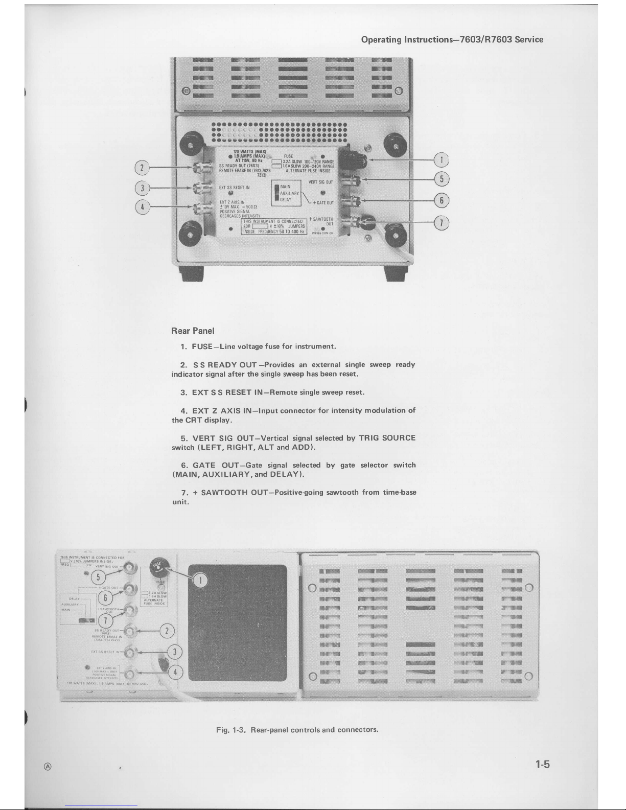
Rear
Panel
1.
FUSE-Line voltage
fuse
for
instrument.
2. SS
READY OUT-Provides
an external single
sweep ready
indicator signal
after the single s,veep
has been reset.
3.
EXT
S S
RESET
lN-Remote single wveep
reset.
4.
EXT Z AXIS
lN-lnput connector
for intensity modulation of
the cRT display.
5. VERT SIG
OUT-Vertical
signal selected by
TRIG SOURCE
switch
(LEFT.
RIGHT,
ALT and ADDI.
6.
GATE OUT-Gate
signal selected by
gate
selector switch
(MAlN,
AUXILIARY, and
DELAYI.
7. + SAWTOOTH
OUT-Positive-going
sawtooth
from time-base
unit.
@
Fig, 1-3, Rear-panel controls and
connectors.
1-5
Page 12
Operating
I nstructions-7603/R7603
Service
7.
Advance
the
INTENSITY
control
until the
trace is
at
the
desired
viewing
level
(near
midrange).
Advance
the
R EADOUT
until the
readout
display
is
at the
desired
viewing
level.
8.
Connect
the 4
V calibrator
pin-jack
to
the input
of
the left
vertical
unit
with a BNC
to
pin-jack
cable
(supplied
accessory).
Display
Focus
9. Adlust
the FOCUS
control
for
a sharp,
well-defined
display
over the
entire trace
length.
lf
a
properly
focused
display
cannot
be
obtained with
the
FOCUS
control.
the
internal
Astigmatism
adjustment
must
be
re-set;
see the
Calibration
section
of this manual.
Trace
Alignment
10. Disconnect
the input
signal
and
position
the
trace
with
the left vertical
unit
position
control
so it
coincides
with
the center
horizontal
line
of the
graticule.
lf
the trace
is
not
parallel
to the center
horizontal
line
of the
graticule,
see Trace
Rotation
adjustment
procedure
in
Calibration
section.
Graticule I
llum ination
11. Rotate
the
GRAT ILLUM
control
throughout
its
range
and notice
that
the illumination
of the
graticule
lines
increases
as the control is
turned
clockwise
(most
obvious
with
tinted f ilter
installed).
Set the
control
so
the
qraticule
lines
are illuminated
as desired.
Vertical
Deflection
System
12.
Connect
the 4
V calibrator
signal
to
the
input
connector
of the left
vertical
unit with
the BNC
to
pin-iack
cable.
Set both
vertical
units for
a deflection
factor
of
one
volt/division.
The
display
amplitude
should
be
four
divisions.
Note
the exact
display
amplitude
for step
15.
13. Notice
that the
position
control
of
onlV the left
vertical
unit has
an effect
on the
position
of the
display.
Position
the
display to
the upper
half
of the
graticule.
14.
Press
the RIGHT
button
of
the VERT
MODE
switch.
Remove
the
calibrator
signal
from
the left
vertical
and connect
it
to
the right
vertical.
The
display
amplitude
should
be
four
divisions
within 0.12
division.
Note
the
exact
display
amplitude
for
the next
step.
i5. A
correct
display in both
steps
12
and 14
indicates
that
the 7603
Vertical
Deflection
System
and
the vertical
1-6
plug-in
units
are calibrated.
lf
the
displays
noted
previously
are both
outside
the
given
tolerance
in
the
same
direction
(i.e.,
high
or
low),
the Vertical
Gain
or 4 Volts
calibrator
adlustment
probably
needs
re-adjustment.
Otherwise.
check
the
calibration
of the vertical
plug-in
units.
16. Notice
that the
position
control
of
only
the right
vertical
unit
has
an effect
on
the
position
of the
display.
Position
the
display
to the lower
half
of
the
graticule.
Set
both
vertical
units
for
a
deflection
factor
of
two
volts/
division.
Connect
calibrator
signal
to
both
vertical
units
bv
using
a
dual
input
coupler.
17. Press
the ALT
button
of the
VERT
MODE
switch.
Notice
that
two traces
are
displayed
on the
CRT.
The
top
trace is
produced
by the
left
vertical
unit
and the bottom
trace is
produced
by
the right
vertical
unit.
Set
the sweep
rate
to 50
milliseconds/division.
Notice
that
the
display
alternates
between
the left
and
right
vertical
units
after
each sweep.
Turn
the sweep
rate switch
throughout
its
range.
Notice
that
the
display
alternates
between
vertical
units
at all sweep
rates.
18.
Press
the CHOP
button
of the VERT
MODE
switch.
Turn
the
sweep
rate
throughout
its
range.
Notice
that
a
dual-trace
display is
presented
at all
sweep
rates,
but
unlike
ALT
both
vertical
units
are displayed
on each sweep
in
a
time-sharing
manner.
Return
the sweep
rate
to 0.5
m il I isecond/d
ivision.
19.
Press
the ADD
button
of the VERT
MODE
switch.
The
display
should
be
four divisions
in
amplitude.
Notice
that the
position
control
of either
vertical
unit moves
the
display.
Return
the
VERT MODE
switch
to LEFT.
Triggering
20.
Center
the
display
on the
CBT
with
the left
vertical
unit
position
control.
Disconnect
the
input
signal
from
the
right
vertical
unit input
connector.
Sequentially
press
all of
the
VERT MODE
switch
buttons.
Notice
that
a stable
display
is
obtained in
all
positions
of the
VERT
MODE
switch
(straight
line in R IGHT
position).
21. Press
the LEFT
button
of
the TRIG
SOURCE
switch.
Again,
sequentially
press
all
of the
VERT MODE
buttons.
Notice
that
the
display is
again
stable in
all
positions,
as
in
the
previous
step.
22.
Press
the RIGHT
button
of the TRIG
SOURCE
switch. Sequentially press
all of the
VERT
MODE
buttons
and notice
that a stable
display
cannot
be
obtained
in
any
position.
This is
because
there is no
input
signal connected
@
Page 13

to
the right vertical
unit. Return the
TRIG
SOURCE switch
to VERT
MODE.
Remove calibrator signal from
left
vertical unit and
connect it to right
vertical
unit.
Repeat
steps
20
ro
22. The trigger signal will come
from
right
vertical.
When the LEFT button
is
pressed
of
the TRIG
SOURCE switch
the displav
is not stable because there is
no input signal
connected to
the left vertical. Return the
TRIG SOURCE switch
to VERT
MODE.
Horizontal
Def lection
System
23. Position the start of
the sweep to the
left
graticule
line with the
time-base unit
position
control.
24. Connect a
10X
probe
to the
input
of the right
vertical
unit. Set the right
vertical unit for a deflection
factor of
10 volts/division and
set the VERT MODE switch
to
RIGHT. Set the time-base
unit for a sweep rate of five
m illiseconds/d iv
ision.
25. Connect the
probe
tip to a
line-voltage source. The
display should show
three complete cycles over the 10
divisions within
0.3 division. A correct display
indicates
that the
7603
Horizontal Deflection System
and
the
time-base
plug-in
unit are
correctly calibrated.
lf
the display
is
outside the
given
tolerance, either the
7603
or the
time-base
unit needs to be recalibrated.
Refer to the
Calibration
section of this manual. and to the time-base
unit manual for adjustment
procedure.
NOTE
This step
is based on an
accurate 60-Hertz line
frequency.
For other line
frequencies,
this
procedure
will need to be changed accordingly.
26. Disconnect
the
probe
from
the
line-voltage
source
and the
right
vertical
unit
and
connect the
probe
to the
left
vertical
unit.
Set the VERT
MODE
switch
to
LEFT
and set
the time-base
unit for
a sweep
rate
of 0.5
millisecond/
division.
Beam
Finder
27. Set the deflection factor of the
left vertical
unit to
0.1 volt/division.
Notice that a square-wave
display
is not
visible. since
the deflection exceeds the scan area of the
CRT.
28. Press and
hold the BEAM FINDER switch. Notice
that the
display
is
returned to the viewing area
in
compressed form.
Increase the vertical
and
horizontal
def lection factors until the displav
is
reduced to about two
divisions vertically and
horizontally
(when
the horizontal
unit is
operated
in
the time-base
mode, change
only the
REV B SEP 1979
Operating I nstructions-7603/R7603
Service
def lection factor
of
the vertical
unit).
Adjust
the
position
controls
of the displayed
vertical
unit
and the time-base
unit to center the compressed display
about the center lines
of
the
graticule.
Release
the
BEAM FINDER
switch. Notice
that the display remains within the viewing
area.
Z-Axis lnput
29. lf
an external signal
is
available
(five
volts
peak-to-
peak
minimum at two
megahertz
or
less), the
function
of
the
EXT Z AXIS input can be
demonstrated. Connect
the
external
signal to both
the
input
of the right vertical
unit
and the EXf Z
AXIS
connector with two BNC
cables
and a
BNC T
connector. Set the
VERT l\4ODE
switch to RIGHT
and
set the vertical unit for
a deflection factor
of two
volts/division. Set
the
time-base
unit for a sweeD
rate which
displays several cycles
of
the signal. Adjust
the
amplitude of
the signal
generator
until intensity modulation
is visible
on
the display.
The
positive peaks
of
the
waveform should be
blanked
out and the
negative
peaks
intensified. Notice
that
the setting of the INTENSITY control
determines the
amount of
intensity modulation
that is visible.
30. Disconnect
the signal
f rom
the EXT Z AX lS
connector, but
leave it connected
to the
right vertical
unit
input.
Check
that
peak-to-peak
amplitude
of the displayed
signal
is
four
divisions
maximum.
31.
This completes
the Operating
Checkout
procedure
for the 7603. Instrument
operations not
explained
here,
or
operations which
need further
explanation
are
discussed
under
General Operating Information.
SIMPLI F I
ED
OPERATING INSTRUCTIONS
The
following information
is
provided
to aid in
quickly
obtaining the correct
setting for
the 7603
controls
to
present
a
display. The
operator
should be familiar
with
the
complete
function and
operation
of this
instrument
as
described
elsewhere
in
this section
before
using
this
procedure.
For
detailed
operating information
for
the
plug-in
units, see
the
instruction
manuals
for the
applicable
u n
its.
Single-Trace Display
The
following
procedure
will
provide
a display
of
a
single-trace
vertical unit
against
one time-base
unit. For
simplicity
of explanation,
the vertical
unit is installed
in
the
left
vertical
compartment. The
right vertical
compartment
can be used if
the
procedure
is
changed
accordingly.
1.
Install
a
7A-series
com
partment.
unit in
the left
1-7
Page 14

Operating
I nstruction
s-7603/R7603
Service
2.
Press
the LEFT
button
of
the VERT
MODE
switch.
3. Install
a
7B-series
time-base
unit
in the
horizontal
com
partment.
4. Press
the VERT MODE
button
of the
TRIG
SOURCE
switch.
5.
Connect
the signal
to the input
connector
of the
vertical
unit.
6. Set
the vertical
unit
for AC input
coupling
and
cal
ibrated
def
lection
factors.
7.
Set
the
time-base
unit
for
auto
mode,
internal
triggering
at a calibrated
sweep rate
of
one millisecond/
d
ivision.
8. Advance
the INTENSITY
control
until
a display
is
visible.
(lf
no display
is visible
with INTENSITy
at
about
midrange,
press
and hold
the BEAM
FINDER
switch
and
adjust
the
vertical
deflection
factor
until
the
display is
reduced
in
size
vertically;
then
center
the
compressed
display with
vertical
and horizontal position
controls;
release
the
BEAM FINDER.)
Adjust
the FOCUS
control
for
a well-def
ined
display.
Adjust
Readout
INTENSITy
for
the
desired
viewing level.
9.
Set the
vertical
deflection
factor
and vertical
position
control
for
a display
which
remains
within
the
qraticule
area vertically.
10. lf
necessary,
set
the time-base
triggering
controls
for
a stable
display.
11.
Adjust
the
time-base
position
control
so
the display
begins
at the left
edge
of the
graticule.
Set
the time-base
sweep
rate
to display
the
desired number
of cyctes.
Dual-Trace
Display
The
following
procedure
will
provide
a display
of two
slngle-trace
vertical
units
against
one time-base
unit.
1 . Install
7A-series
vertical
units in
both
vertical
plug-in
com
partments.
2. Press
the LEFT
button
of the VERT
MODE
switch.
1-8
3. Install
a
7B-series
time-base
unit
in
the horizontal
com
partment.
4.
Press
the VERT
MODE
button
of the TRIG
SOURCE
switch.
5.
Connect
the
signal
to
the input
connectors
of the
vertical
units.
6. Set
the
vertical
units
for AC
input
coupling
and
cal ibrated
def lection
factors.
7.
Set
the
time-base
unit
for
auto
mode,
internal
triggering
at a sweep
rate
of
one millisecond/division.
8. Advance
the INTENSITY
control
until
a display
is
visible.
(lf
no
display
is visible
with lNTENSlry
at
midrange,
press
and hold
BEAM
FINDER
switch
and
adjust
vertical
deflection
factor
until
display
is
reduced
in
size
vertically;
then
center
compressed
display
with
vertical
and
horizontal position
controls;
release
the
BEAM
FINDER
switch.)
Set
the FOCUS
control
for
a
well-defined
display.
9. Set
the left
vertical
unit
def lection
factor
for
a display
about
four
divisions
in
amplitude.
Adjust
the left
vertical
position
control
to move
th is d isplay
to the
top
of the
graticule
area.
10.
Press
the RIGHT
button
of the
VERT
MODE
switch.
1
1.
Set the
R IGHT
vertical
unit
def lection
f actor
for
a
display
about four
divisions in
amplitude
(if
display
cannot
be
located,
use
BEAM FINDER
switch).
position
this
display
to the
bottom
of the
graticule
area
with
the
right
vertical
unit
position
control.
12. Press
the ALT
or CHOP
button
of the
VERT
MODE
switch.
A
dual-trace
d
isplay
of
the
signal
f rom
the left
vertical
and right
vertical
plug-in
units
should
be
presented
on
the CRT.
(For
more information
on choice
of dual-trace
mode,
see Vertical
Mode
in
this
section.)
13. lf
necessary,
adjust the
time-base
triggering
controls
f
or a stable
d isplay.
'l
4.
Adjust
the
time-base
position
control
so
the display
begins
at the left
edge
of the
graticule.
Set
the
time-base
sweep
rate
for
the
desired horizontal
display.
@
Page 15

Delayed
Sweep
-
Single
Trace
)
fne
following
procedure
will
provide
a delayed
sweep
display
of
a single-trace
vertical
unit.
1. Follow
the complete
procedure
given
under
Single-Trace
Displays.
2.
Be
sure the
time-base
unit installed
in
the
horizontal
compartment
is
a dual
time-base
with
delaying/delayed
caoabilities.
3.
Follow
the
procedure
given
in
the instruction
manual
for
the
dual
time-base
unit
to
obtain
a delayed-sweep
display.
Delayed
Sweep
-
Dual
Trace
The
following
procedure
will
provide
a delayed-sweep
display
of two single-trace
vertical
units.
1. Follow
the complete
procedure
given
under Dual-
Trace
Display.
\
j
2.
Be sure
the
time-base
unit installed
in
the horizontal
'
compartment
is
a dual time-base
unit with
delaying/delayed
capab i
I ities.
3.
Follow
the
procedure
given
in
the
instruction
manual
for
the dual
time-base
unit
to obtain
a
delayed-sweep
display.
X-Y
Display
The
following
procedure
will
provide
an
X-y
display
(one
signal versus
another rather
than
against
time).
NOTE
Some 7B-series
time-base
units
have
provisions
for
amplif
ier
operation
in the X-Y
mode;
see X-Y
operation
in
this section for
details
of operation
in
this manner.
'l
. Install
7A-series
amplif ier
units
in
both
the left
vertical
and
the horizontal
compartments.
2.
Press
the
LEFT
button
of
the VERT
MODE
switch.
@
Operating
I nstructions-7603/R7603
Service
3.
Connect
the X-signal
to the
amplifier
unit
in the
horizontal
compartment.
4.
Connect
the Y-signal
to
the
vertical
compartment.
amplif ier
unit in
the left
5. Set
both
amplifier
units
for AC
input
coupling
and
cal ibrated
def
lection
factors.
6. Advance
the INTENSITY
control
until
a
display is
visible.
(lf
no
display is
visible,
press
and hold
BEAM
FINDER
switch
and adjust the
def
lection
factors
of
both
amplifier
units
until
display is
reduced
in
size both
vertically
and horizontally;
then
center
compressed
display
with
the
position
controls;
release
the BEAM
FINDER
switch.)
Adjust
the FOCUS
control
for
a well-defined
d isp lay.
GENERAL
OPERATING
INFORMATION
Intensaty
Control
The
setting
of the INTENSITY
control
mav
affect
the
correct
focus
of the d isplay.
Slight
re-ad
justment
of the
FOCUS
control
may
be necessary,
when
the intensity
level
is
changed.
To
protect
the
CRT
phosphor;
do not
turn
the
INTENSITY
control
higher
than
necessary
to
provide
a
satisfactory
display.
The
light
filters
reduce
the
observed
light
output
from
the
CRT. When
using
these
f ilters,
avoid
advancing
the INTENSITY
control
to
a setting
that may
burn
the
phosphor.
When
the
highest
intensity
display
is
desired,
remove
the
f ilters
and
use
only
the
clear
faceplate
protector (permanently
installed
behind
bezel).
Apparent
trace intensity
can
also be
improved
in
such
cases
bv
reducing
the
ambient
light
level
or using
a viewing
hood.
Also,
be
careful
that the INTENSITY
control
is
not
set
too
high
when
changing
the time-base
unit
sweep
rate
from
a
fast
to
a slow
sweep
rate,
or when
changing
to
the
X-y
mode
of
operation.
The instrument
incorporates protection
circuitry
which
automatically
reduces
the
display intensity
to
a lower
level
when
the
time-base
unit
is
set
to
a slow
sweep
rate. This
reduces
the danger
of
damaging
the
CRT
phosphor
at these
slower
sweep
rates.
Display
Focus
The
FOCUS
control
allows
adjustment
for
best
defini-
tion
of the
CRT
display. The
Readout
intensity
should
be
turned
on, when
adjusting
the
Focus
control.
Slight
re-adjustment
of
this control
may
be
necessarV
as
the
display
conditions
change. lf
a
properly
focused
display
cannot
be
obtained
with the
FOCUS
control,
the internal
Astigmatism
adjustment
must
be
re-set;
see
the Calibration
section
of this manual.
1-9
Page 16

Operating
I nstructions-7603/R7603
Service
Graticule
The graticule
of the 7603 is marked
on the inside
of the
faceplate
of the CRT,
providing
accurate, no-parallax
measurements.
The
graticule
is
divided into
eight vertical
and ten horizontal
divisions. Each
division is
1.22 centi-
meters
square.
In
addition,
each major division
is
divided
into
five minor
divisions.
The
vertical
gain
and
horizontal
timing
of the
plug-in
units
are calibrated
to
the
graticule
so
accurate measurements
can be
made from
the CRT. The
illumination
of the
graticule
lines
can be varied
with
the
GRATICU LE I LLUM
control.
NOTE
Two
types
of crt
graticules
have
been
used in
some
Tektronix
orcillorcopes.
One
graticule
has
0%
and
100o1' risetime
reference
points
that are separated
by
6
vertical
graticule
divisions.
The other
graticule
has
the 0%
and
100% risetime
reference
points
separated
by 5 vertical
divisions.
ln
your
manual,
illustrations
of
the
crt
face or risetime
measurement
instructions
may
not
correspond
with
the
graticule
markings
on
your
oscilloscope.
Fig. 1-4
shows the
graticule
of
the
7603
and def ines
the
various
measurement
lines. The
terminology
defined
here
will be used in
all discussions involving graticule
measure-
ments. Notice
the 0%,
1oyo,goyo
and 100%
markings
on
the
left
side
of the
graticule.
These
markings
are
provided
to
facil itate
risetime measurements.
Light Filter
The
tinted f ilter
provided
with
the 7603 minimizes
light
ref lections from
the face
of the
CRT to improve
contrast
when
viewing
the
display under
high
ambient light
condi-
tions. This
filter should be
removed
for
waveform
photo-
graphs
or when viewing
high writing
rate
displays. To
remove
the filter,
loosen the
two screws
on
the
riqht side
of
Fig,
1-4, Def inition
of
measurement
lines
on 7603
graticule,
1-10
the bezel
and remove
the bezel. Remove
the
tinted
filter;
leave
the clear
plastic
faceplate
protector
installed
and
replace
the bezel. The
faceplate
protector
should
be left in
place
at
all times to
protect
the
CRT faceplate
from
scratch es.
An
optional
mesh filter
is
available
for
use
with
the
7603. This
filter
provides
shielding
against
radiated
EMI
(electro-magnetic
interference)
from
the face
of the
CRT. lt
also serves
as a light
filter
to make
the
trace
more
visible
under high
ambient light
conditions.
The
mesh
f
ilter
f its in
place
of the
plastic
CRT
mask
and
the tinted
filter.
Beam Finder
The BEAM
FINDER
switch
provides
a means
of
locating
a display
which
overscans the viewing
area
either vertically
or
horizontally.
When
the BEAM FINDER
switch is
pressed
and held,
the display is compressed
within
the
graticule
area.
Release
the BEAM FINDER
switch
to return
to
a
normal
display. To
locate
and reposition
an
overscanneo
display,
use the
following
procedure:
1.
Press
and hold the BEAM
FINDER
switch.
2.
Increase
the vertical
and horizontal
deflection
factors
until the vertical
deflection
is reduced
to
about two
divisions
and the horizontal
deflection
is
reduced
to
about
four
divisions
(the
horizontal
deflection
needs
to be
reduced
only
when
in
the X-Y
mode
of operation).
3. Adjust
the vertical
and horizontal
position
controls
to
center
the
display
about the vertical
and horizontal
center
I i nes
of th
e oraticu
le.
4.
Release
the BEAM FINDER
switch;
the
display
should remain
within
the viewino
area.
Readout
Modes
The
characters
of the readout
display
are written
by
the
CRT beam
on
a time-share
basis with
signal
waveforms.
The
Readout
system
operates in
a
free running
mode
to
randomly interrupt
the
waveform
display
to
present
the
readout
characters.
The
readout
system
can
also
operate in
a GATE TRIG'D
mode. No
readout
signal is
produced
until
after
the
sweep has
occurred.
In
this mode
the
sweep
musr
run
to have
the readout
d isplayed.
Display Photography
A
permanent
record
of the CRT
display
can
be
obtained
with
an
oscilloscope
camera system.
The
instruction
manuals
for
the TEKTRONIX
Oscilloscope
Cameras
include
complete instructions
for
obtaining waveform
photographs.
The
following
specif ic information
applies to
the 7603.
(
,0
REV
C
SEP 1979
Page 17

The
CRT bezel
of
the 7603
provides
integral
mounting
for a TEKTRONIX
Oscilloscope
Camera. The
three
pins
;located
on the
left
side
of the CRT bezel
connect
power
to
compatible camera
systems.
lt
also
receives control
signals
from TEKTRONIX
automatic cameras
to
allow camera-
controlled
single-shot
photography
(see
camera
manual for
f urther information).
Vertical Mode
Left and Right Mode.
When
the
LEFT
or
RIGHT
button
of
the
VERT MODE
switch
is
pressed,
only the signal
from
the
plug-in
unit
in
the selected
compartment is
displayed.
Alternate
Mode.
The ALT
position
of the VERT
MODE
switch
produces
a display which
alternates between
the
plug-in
units in
the
left
vertical
and right vertical
compart-
ments
with each sweep
of the CRT. Although
the ALT
mode can be
used
at all sweep rates,
the CHOP mode
provides
a more satisfactory
display
at sweep rates below
about 20 milliseconds/division.
At
these slower
sweep rates,
alternate-mode switching becomes
visually
perceptible.
NOTE
This instrument
will not operate in
the ALT
mode if
the horizontal
plug-in
unit is
not operated in
the
time-base
mode.
The
TRIG SOURCE
switch
allows selection
of the
triggering
for an alternate display. When
this
switch is set
to
the VERT MODE
position,
each sweep is
triggered by
the
signal being
displayed on the
CRT.
This
provides
a stable
display of two unrelated signals,
but
does
not indicate
the
time relationship between
the signals. In
either the LEFT
or
RIGHT
positions
of
the TRIG
SOURCE
switch, the two
signals
are displayed showing
true time
relationship.
However, if
the signals
are
not
time-related, the
display
from the
plug-in
unit
which is
not
providing
a trigger signal
will appear unstable
on
the CRT.
Chopped Mode. The
CHOP
position
of the VERT
MODE
switch
produces
a display which
is
electronically
switched between channels
at a one-megahertz rate. In
general,
the CHOP
mode
provides
the
best
display
at
sweep
rates lower than
about
20 milliseconds/division,
or when-
ever dual-trace single-shot
phenomena
are to be displayed.
At faster sweep rates,
the
chopped
switching becomes
apparent and
may interfere with
the display.
Correct internal triggering for the CHOP mode
can be
obtained
in
any of the three
positions
of the TR lG
)SOUnCe
switch. When the TRIG SOURCE
switch
is
set to
'
VERT MODE,
the
internal
trigger signals
from the vertical
(A
Operating I nstructions-7603/R7603
Service
plug-in
units
are algebraically
added
and the time-base
unit
is
triggered from
the resultant
signal.
Use of the LEFT
or
RIGHT
trigger-source
positions
trigggers
the time-base
unit
on the internal
trigger signal
from the
selected
vertical
unit
only.
This
allows
two time-related
signals
to be
displayed
showing
true
time relationship.
However,
if
the signals
are
not time-related,
the display from
the channel
which is
not
providing
the
trigger signal
will appear
unstable. The
CHOP
mode
can be used
to compare
two single-shot,
transient,
or
random
signals
which
occur within
the time
interval
determined
by the
time-base
unit
(ten
times selected
sweep
rate). To
provide
correct triggering,
the display
which
provides
the trigger signal
must
precede
the second
display
in
time.
Since the
signals show
true
time relationship,
time-difference
measurements
can be
made from
the
display.
Algebraic
Addition.
The ADD
position
of the VERT
MODE
switch can
be used to
display the
sum
or difference
of two signals,
for common-mode
rejection
to remove
an
undesired signal,
or for DC
offset
(applying
a
DC voltage
to
one
channnel
to
offset the DC component
of a signal
on the
other channel). The common-mode
rejection
ratio between
the vertical
plug-in
compartments
of the 7603 is
greater
than 20:1
at 50 megahertz. The
rejection
ratio
increases
to
100:'l
at DC.
The
overall
deflection factor
on
the
CRT in
the
ADD
mode is
the resultant
of the
algebraic addition
of the
signals
from
the two vertical
plug-in
units. lt is
difficult
to
determine
the voltage
amplitude
of the resultant
display
unless the
amplitude
of the signal
applied
to one of
the
plug-in
units is
known. This is
particularly
true
when the
vertical
units
are set to different
deflection
factors,
since it
is not
obvious
which
portion
of the
display is
a result of the
signal
applied to either
plug-in
unit.
Also,
the
polarity
and
repetition
rate
of the applied
signals
enters into
the
calcu lation.
The
following
general
precautions
should be
observed
to
provide
the
best
display when
using the ADD
mode:
1. Do not
exceed the input
voltage rating
of
the
plug-in
u n its.
2. Do not
apply large signals
to the
plug-in
inputs.
A
good
rule to follow is not
to
apply a signal
which exceeds
an
equivalent of about
eight times
the vertical
deflection
factors. For
example,
with a vertical
def lection
factor
of
0.5
volt/division, the voltage
applied to that
plug-in
unit
should
not
exceed
4 volts.
Larger
voltages may
result in
a
distorted display.
3. To
ensure
the
greatest
dynamic
range
in the ADD
mode, set the
position
controls
of the
plug-in
units to
a
1-1
1
Page 18

Operating
I nstructions-7603/R7603
Service
setting
which would
result in
a mid-screen
display if
viewed
in
the LEFT
or
RIGHT
positions
of the VERT
MODE
switch.
4.
For
similar response
from
each channel,
set
the
plug-in
units for
the same input
coupling.
Trigger
Source
The
TRIG
SOURCE
switch
allows
selection
of the
internal
trigger
signal
for
the
time-base
unit.
For
most
applications,
this
switch
can be
set
to the
VERT
MODE
position.
This
position
is
the most
convenient,
since
the
internal
trigger
signal
is
automaticallv
switched
as the
VERT
MODE
switch is
changed,
or
as the
display
is
electronically
switched
between
the left
vertical
and right
vertical
plug-in
units in
the ALT
position
of the VERT
MODE
switch.
lt
also
provides
a
usable
trigger
signal in
the
ADD
or CHOP
positions
of the VERT
MODE
switch.
since
the internal
trigger
signal
in
these
modes
is
the
algebraic
sum
of
the signals
applied
to
the vertical plug-in
units.
Therefore,
the
VERT IVIODE position
ensures
that
the
time-base
unit
receives
a trigger
signal
regardless
of the
VERT
MODE
switch
setting,
without
the
need
to chanqe
the
trigger
source
selection.
lf
correct
triggering
for
the
desired
display
is
not
obtained
in
the
VERT
MODE
position.
the
LEFT
or
RIGHT
positions
can
be
used
to
obtain
the
trigger
signal
from
either
the left
vertical
or right
vertical
plug-in
unit.
The internal
trigger
signal
is
obtained
from
the
selected
vertical
compartment,
whether
the
plug-in
unit in
that
compartment
is
selected
for
display
on the
CRT
or not.
lf
the internal
trigger
signal
is
obtained
from
one
of the
vertical
units, but
the
other
vertical
unit is
selected
for
display,
the internal
trigger
signal
must
be
time-related
to
the
displayed
signal
in
order
to
obtain
a triggered
(stable)
d isplav.
X-Y
Operation
In
some
applications,
it is
desirable
to
display
one
signal
versus
another
(X-Y)
rather
than
against
time
(internal
sweep).
The
flexibility
of the
plug-in
units
available
for
use
with
the 7603
provides
a
means
for
applying
an
external
signal
to the
horizontal
deflection
system
for
this
tvpe
of
display.
Some
of the
7B-series
time-base
untts
can
be
operated
as amplifiers
in
addition
to
their
normat
use
as
tinre-base
generators.
This
feature
allows
an
external
signal
to
provide
the horizontal
def lection
on the
CRT. For
most
of the
time-base
units
with
the
amplifier
function,
the
X
(horizontal)
signal
can be
connected
either
to
an
external
Input
connector
on
the time-base
unit
or
it
can
be
routed
to
the time-base
unit through
the internal
triggerrng
sysrem
(see
time-base
instruction
manual
f
or details)
. lf
the latter
method
is
used,
the TRIG
SOURCE
switches
must
De
set so
that
the
X
(horizontal)
signal
is
obtained
from
one
of the
1-12
vertical
units
and
the Y
(vertical)
signal is
obtained
from
the
other
vertical
unit.
The
advantages
of
using
the internal
tngger
system
to
provide
the
X
signal
are
that
the
attenuator
switch
of the
amplifier
unit providing
the
horizontal
signal
determines
the
horizontal
deflection
factor
to
allow full-range
operation
and the
plug-in
units
do
not
have
to
be
moved
between
compartments
when
X_y
operation
is desired.
Another
method
of
obtaining
an X-y
display
is
to install
an amplif
ier
plug-in
unit in
one
of the
horizontal plug_in
compartments
(check
amplifier
unit gain
as
given
in
the
plug-in
instruction
manual
to
obtain
calibrated
horizontal
deflection
factors).
This
method provides
the best
X-y
display,
particularly
if
two identical
amplifier
units
are
used,
since
both
the
X
and Y
input
systems
will
have
the
same
delay
time, gain
characteristics,
input
coupling,
etc.
For
further
information
on
obtaining
X-y
displays,
see
the
plug-in
unit
manuals.
Also,
the
reference
books
listed
under
Applications
provide
information
on
X-y
measurements
and
interpreting
the resultant
lissajous
displays.
Intensity
Modulation
Intensity
(Z-axis)
modulation
can
be
used
to
relate
a
third item
of
electrical
phenomena
to
the vertical
(y-axis)
and
the
horizontal
(X-axis)
coordinates
without
affectino
the
waveshape
of the
displayed
signal.
The
Z-axis
modul
I
lating
signal
applied
to
the CRT
circuit
changes
the
I
intensity
of the
displayed
waveform
to
provide
this
type
of
display.
"Gray
scale"
intensity
modulation
can
be
obtained
by
applying
signals
which
do not
completely
blank
the
display.
Large
amplitude
signals
of the
correct
polarity
will
completely
blank
the
display;
the
sharpest
display
is
provided
by
signals
with
a fast
rise
and
fall. The
voltage
amplitude
required
for
visible
trace
modulation
depends
upon
the
setting
of the INTENSITY
control.
A
two_volt
peak-to-peak
signal
will
completely
blank
the display
even
at maximum
intensity
levels.
Lower
amplitude
signals
can
be
used
to
only change
the
trace
brightness
rather
than
completely
blank
the
display.
Negative-going
modulating
signals
increase
the
display
intensity
and
positive-going
modulating
signals
decrease
the
display
intensity.
Useful
input
frequency
range
is
DC
to 10
megahertz
(input
voltage
derating
necessary
above
two
megahertz).
The
maxrmum
input
voltage
should
be limited
to 10
volts
(DC
plus
peak
AC).
Time
markers
applied
to
the
EXT
Z
AX lS
input
connector provide
a direct
time
reference
on the
display.
With
uncalibrated
horizontal
sweep
or
external
horizontal
mode
operation,
the
time
markers
provide
a means
of
reading
time
directly
from
the
display.
However,
if
the
markers
are not
time-related
to
the
displayed
waveform,
a
single-sweep
display
should
be
used
(for
internal
sweep
only)
to
provide
a stable
display.
@
Page 19
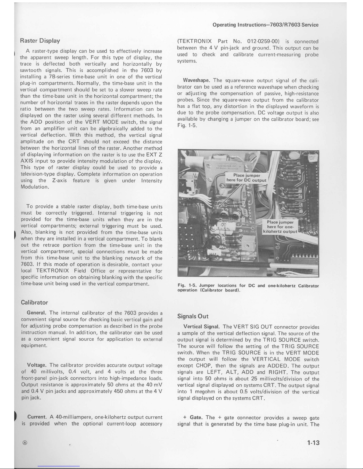
Raster
Display
A
raster-type
display
can be used to
effectively
increase
the apparent sweep length. For
this type of display, the
trace is
deflected
both vertically
and horizontally by
sawtooth signals. This is
accomplished in the 7603 by
installing a 7B-series
time-base unit in
one of the
vertical
plug-in
compartments. Normally,
the
time-base
unit in the
vertical
compartment should be set to
a slower sweep rate
than the time-base unit in
the horizontal compartment;
the
number
of horizontal traces in the raster
depends upon the
ratio between
the two sliveep rates. Information
can be
displayed
on the raster using several
different
methods. ln
the
ADD
position
of the VERT MODE
switch,
the
signal
from an amplifier unit can be
algebraically
added
to the
vertical
deflection.
With
this method,
the vertical signal
amplitude on the CRT should not
exceed the distance
between
the horizontal lines
of the raster. Another
method
of displaying information
on the raster is to
use the
EXT
Z
AXIS
input
to
provide
intensity modulation
of the
display.
This
type
of
raster
display could be
used to
provide
a
television-type display. Complete information
on operation
using the Z-axis
feature is
given
under Intensity
Modulation.
To
provide
a
stable
raster display. both
time-base
units
must be correctly
triggered. Internal
triggering
is
not
provided
for the time-base
units
when they
are
in the
vertical compartments;
external
triggering must be
used.
Also, blanking
is not
provided
from the
time-base units
when they
are
installed
in a vertical
compartment. To
blank
out the retrace
portion
from the time-base
unit
in
the
vertical
compartment,
special connections
must be made
from
this time-base
unit to the blanking
network
of
the
7603.
lf this mode
of operation is
desirable, contact
your
local TEKTRONIX
Field
Office or representative
for
specif ic information
on obtaining blanking
with the specif ic
time-base unit being
used
in
the vertical
compartment.
Calibrator
General. The internal
calibrator
of
the 7603
provides
a
convenient signal source for
checking basic
vertical
gain
and
for
adjusting
probe
compensation
as
described in the
probe
instruction
manual.
In
addition, the calibrator can
be used
as a
convenient
signal source for
application to
external
equ ipment.
Voltage. The
calibrator
provides
accurate output voltage
of
40 millivolts,0.4
volt,
and
4 volts
at the three
front-panel
pin-jack
connectors
into
high-impedance loads.
Output resistance is
approximately 50 ohms
at
the 40 mV
and
0.4
V
pin
jacks
and
approximately
450
ohms at the 4 V
pin
jack.
Current. A 40-milliampere,
one-kilohertz output current
is
provided
when
the optional current-loop
accessory
tA)
Operating
I nstructions-7603/R7603
Service
(TE
KTRON lX Part
No. 012-0259-00)
is connected
between
the 4 V
pin-jack
and
ground.
This
output
can
be
used to check and calibrate
current-measuring
probe
systems.
Waveshape.
The
square-wave output signal
of the cali-
brator
can be used
as a
reference
waveshape
when checking
or adjusting the compensation
of
passive,
high-resistance
probes.
Since
the square-wave output
from the calibrator
has a flat
top, any distortion in
the displayed
waveform
is
due
to the
probe
compensation.
DC voltage
output is
also
available by changing
a
jumper
on the calibrator
board; see
Fis.
1-5.
Fig.
1-5. Jumper
locations for
DC
and one-kilohertz
Calibrator
operation
(Calibrator
board).
Signals Out
Vertical
Signal.
The
VERT
SIG OUT
connector
provides
a sample
of the vertical deflection
signal. The
source
of
the
output signal is
determined by the TRIG
SOURCE
switch.
The source
will follow the
setting of the TRIG
SOURCE
switch. When the TRIG
SOURCE is in
the VERT MODE
the
output will follow the VERTICAL
MODE
switch
except CHOP. then
the signals
are
ADDED.
The
output
signals
are
LEFT, ALT,
ADD
and RIGHT. The
output
signal
into
50 ohms
is
about 25
millivolts/division
of the
vertical signal
displayed on systems
CRT. The
output signal
into 1
megohm is
about
0.5
volts/division
of the
vertical
signal
displayed on the systems
CRT.
+
Gate. The
+
gate
connector
provides
a sweep
gate
signal that is
generated
by
the time base
plug-in
unit. The
hele for
one-
kiloherle outpul
1-13
Page 20

Operating I nstructions-7603/R7603
Service
gate
selector switch
provides
three
gates
MAIN,
AUXILIARY
and DELAY. The
duration
of the
gate pulse
is
determined by the respective
sweep. Auxiliary
and Delay
gates
can
only be
produced
by dual
sweep
time
base
plug-in
units. The
amplitude
of the
gate
signal
is
about 50
millivolts
into
50 ohms
or
10 volts into
1 meoohm.
+
Sawtooth. The
+
sawtooth connector
provides
a
positive
going
sample
of the
sawtooth
from the time base
unit
in
the horizontal comoartment. The rate
of
rise
of the
sawtooth
signal
is
about 50 millivolts/unit
of
time into
50
ohms or
'1
volt/unit of time
into 1 megohm.
Unit
of
time is
determined by the
time/division
switch
of the
horizonal
plug-in
unit.
Applications
The
7603
Oscilloscope and
its
associated
plug-in
units
provide
a
very f lexible measurement
system. The
capa-
bilities
of
the
overall system depend mainly upon
the
plug-in
units that are chosen for use with
this
instrument.
Specific
applications for the
individual
plug-in
units
are
described in the
plug-in
manuals. The
overall system can
also be used for many
applications which
are
not described
in
detail either in this manual
or
in
the manuals for
the
individual
plug-in
units. Contact
your
local TEKTRON
lX
Field
Office or representative for
assistance in making
specif
ic
measurements with
this
instrument.
The
following books describe
oscilloscope measurement
techniques
which can be adapted
for use with
this
instru me nt.
John
D.
Lenk,
"Handbook
of Oscilloscopes, Theory,
and
Application",
Prentice-Hall Inc.,
Englewood
Cliffs, New
Jersev. i968.
J. Czech,
"Oscilloscope
Measuring
Techniques",
Springer-Verlag, New
York,
1965.
J. F.
Golding,
"Measuring
Oscilloscopes",
Transatlantic
Arts,
Inc.,
197 1.
Charles
H. Roth
Jr..
"Use
Programmed
text, Prentice-Hall
New
Jersev,
1970.
of the
Oscilloscope",
A
Inc.,
Englewood
Cliffs,
Repackaging
for
Shipment
lf
the Tektronix instrument
is
to be shipped
to a Tektronix
Service Center for
service
or
repair,
attach
a tag showing:
owner
(with
address)
and
the
name
of
an
individual
at
Vour
firm
that can
be
contacted,
complete
instrument
serial
number
and a
description
of
the service required
Save
and
re-use
the
package
in which
your
instrument
was
shipped.
lf
the original
packaging
is unfit for
use
or
not
available, repackage
the
instrument
as
follows:
Surround the instrument
with
polyethylene
sheeting
to
protect
the f inish
of the instrument.
Obtain a carton
of
corrugated
cardboard
of the correct carton
strength
and
having
inside
dimensions of no less
than six inches more
than the
instrument
dimensions.
Cushion the instrument
by tightly
packing
three inches
of dunnage
or urethane
foam
between carton
and
instrument,
on all sides. Seal
carton with
shipping tape or industrial
stapler.
The carton test strength for
your
instrument
is 375
pounds.
(
1-14
REV, B- NOV.
1976
Page 21

Section 2-7 603 |
R7
603 Service
lnformation
given
in
this
manual applies to
the R7603
Oscilloscope
also,
unless otherwise
indicated. The R7603
is
electrically
identical to the
7603, but
it is
adapted
for
mounting
in a standard
19-inch rack.
Rackmounting
instructions and a
dimensional drawing
for the
R7603 are
given in
Section
6.
This
instrument will
meet the
following
electrical
specif
ications after complete
calibration
as
given
in
Section
5.
The Operating Checkout
procedure
which
is
given
in
Section
1
provides
a convenient
method
of
checking
instrument
performance
without
making internal checks
or
adjustments.
The
following electrical characteristics apply
over an ambient
temperature
range of 0oC
to
+50"C,
except
as
otherwise
indicated.
Warmup time
for
given
accuracy
is
20
minutes. Limits and
tolerances
given
in the Supplemental
Information
column are
provided
for user information only,
and
should
not be
interpreted as
Performance
Reouirements.
NOTE
Many of the measurement capabilities of this
instrument are determined by the choice of
plug-in
units. The
following characteristics apply to the 7603
Oscilloscope only. See the System Specification at
the end
of
this section for specifications
of the
complete svstem.
SPECIFICATION
VERTICAL
DEFLECTION SYSTEM
Characteristic
Performance
Requ
irements Supplemental
I nformation
Deflection
Factor
Compatible
with
all
7000-series
plug-in
u n
its.
Between Compartments
Within 1%.
Low Frequency
Linearity 0.1 division
or
less compression or
expansion
of a
center-screen 2 division
signal
when
positioned
anywhere
ver-
tically
within the
graticule
area.
Bandwidth
See system
specifications
for 7000-series
I nstru m
en
ts.
7603 Vertical
Amplif
ier
only
(6
div
Reference; 0"C to
150"C)
DC
to at
least 1 15
MHz.
Step
Response
Risetime
See system
specifications
for 7000-series
instruments.
I
solation
Between Vertical
Compartments
At
least 100:1
f rom DC to 100 MHz.
Delay
Line
Permits
viewing
leading
edge of trigger
srgnal.
Chopped
Mode
Repetition
Rate
1
MHz within 20%.
Time Segment
From Each
Compartment
0.4 ro
0.6
ps
REV.8,
NOV.1976
2-1
Page 22

Specif ication
-7603/R7603
Service
VERTICAL
DEFLECTION
SYSTEM
(cont)
Characteristic
Performance
Requ
irements
Supplemental
I nformation
Difference
In
Delay
Between
Vertical
Compartments
0.5 ns
or less.
Vertical
Display Modes
LEFT:
Left vertical
unit only.
ALT:
Dual trace,
alternate between
verti-
cal units.
ADD : Added
algebraically.
CHOP: Dual trace,
chopped between
ver-
tical units.
RIGHT:
Right
vertical unit
only.
Selected by
VERT
MODE
switch.
TRIGGERING
Characteristic
Trigger
Source
Supplemental
Information
Selected
bv
TRIcGER
SOURCE
Perform
ance R equ
irements
LEFT
VERT:
From left
vertical
onlv.
VERT MODE:
Determined
bv
vertical
mode.
RIGHT
VERT:
From
right
vertical
only.
HOR
IZONTAL
DE F LECT
ION
SYSTEM
Characteristic
Fastest
Calibrated
Sweep
Rate
Perform
ance R equ
irements
5
ns/d iv.
Supplemental
I
nformation
Deflection Factor
Compatible
with
all 7000-series plug-in
u n its.
Low Frequency
Linearity
0.1 div
or
less
compression
or
expansion
of a center-screen
2
div
signal
when
positioned
anywhere
horizontally
within
the
graticule
area.
Phase
Shift
Between
the Vertical
and
Horizontal
Amolifiers
Less
than 2"
from DC
to 35 kHz.
F requency
Response
Bandwidth
(8
div Reference)
At least
2 MHz.
2-2
@
Page 23

Specif ication-7603/R
7603
Service
CALIBRATOR
Characteristic
Performance
Requ
irements
Supplemental
I nformation
Waveshape
Positive-going
squarewave
or DC
(DC
voltage
selected
by internal
jumper).
Voltage
Output
Range
40
mV,0.4
V,
and 4 V.
Into
1 M(-2
load.
Voltage
Output Accuracy
+15oC
to
+35"C
Within
1%.
ooC
to
+50"c
Within
2%.
Current
Output Accuracy
40
mA.
+15"C
to
+35oC
Within
2%.
With
optional
current
roop
accessorV
(012-0259-00)
connected
between
4
V
pin
jack
and
ground pin
jack.
ooC
to
+5ooc
Within
3%.
Repetition
R
ate
Approximately
1 kHz.
Output Resistance
40
mV
and 0.4 V
Approximatelv
50
.fl.
4V
Approximately
450
f,I.
EXTERNAL
Z
AXlS
INPUT
Characteristic
Performance
Requ
irements
Supplemental
I
nformation
Sensitivity
(Full
Intensity
Range)
2
V
peak
to
peak.
Useful lnput
Voltage
Versus
Repetition
Frequency
2 V
peak
to
peak,
DC
to 2 MHz;
reducing
to 0.4 V
peak
to
peak
at
10
MHz.
Polarity
of Operation
Positive-going
signal
decreases
intensity.
Maximum
Input
Voltage
10
V
(DC
to
peak
AC).
lnput
Resistance
Approximatelv
500 C2.
OUTPUTS
Characteristic
Camera Power
(P1041
at CRT
Pin
1
-
+15
V
Pin
3 - single
sweep
reset
Supplemental
I
nformation
Pin 5
-
ground
Page 24
Specif ication
-7603/R7603
Service
CHARACTER
GENERATOR
Characteristic Performance Requ
irements
Su
pplemental
I nformation
Character
Size
Ad
justable.
Modes
of Ooeration
Free-run independent
of sweep.
Selected bv internal
R EADOUT
mode
switch.
Triggered
after sweep.
DISPLAY
(CRT)
and
OPTIONS
Characteristic Performance
R equ irements
Supplemental
I nformation
Cathode Ray Tube Type
T
7400.
G
raticu le
TyPe Internal
and
illuminated.
Area
8 X
'10
div.
Standard 1 div
equals
1.22 cm.
Option
4
1 div equals 1 cm.
Option 6 1 d iv
equals 1.22 cm
(Spectrum
Analyzer).
Phosphor
Standard P31
Option
78
P1 1 others on
request.
Beam F inder
Limits
display
to within
graticule
area
when BEAM FINDER
switch is
actuated.
Photographic Writing
Specif ications
C53 Camera
(/1.9
Lens
1
:0.85 lmage-to-Object
R
atio)
Phosphor
Standard
Option
4
Polaroidr
film
type 107
(3000
ASA).
Without film
fogging techniques.
P31
P11
100 div/ps
140 div/ps
180
cmlgs
260
cm/ps
1
Registered trademark Polaroid Corporation.
2-4
REV
NOV 1981
Page 25

Specif ication
-7
603 I R7
603 Service
POWER
SOURCE
Ma
(11
Characteristic
Performance
Requ
irements
Supplemental
I nformation
Line
Voltage
Ranges
1 10 V nominal
100v
!10%.
110 V
r10%.
120V
!10y..
220 V nominal
200v
t10yo.
22O
V
!1OYo.
240 V
!10%.
Line Frequency
50
to 60
Hz
(R7603
and
7603)
(7603
8010100
to 8368864, 50
to
400 Hz)
R7603 and
7603 Option 5,
50 to
400 Hz.
4aximum
Power
Consumption
115 V AC;
60 Hz)
170
W,
1.9 A.
Fuse
Data
110
V
line
(Fi000)
See Electrical
Parts
List
for
fuse
information.
220Y
line
(F1000)
+130
V
Supply
(F855)
SIGNALS
OUT
Performance
Requ
irements
See
systems
specifications
for 7000-series
instru
ments.
LEFT,
RIGHT,
ALT,
and ADD.
C haracteristic
VERT
SIG
OUT
Vertical
Signals
Supplemental
I nformation
Selected
by TR lG
SOURCE
25
mV/div.
0.5 V/div.
+20%
system
cRT
to VERT
SIG
OUT.
5 ns
or
less.
Gain
Into
50 Q
Into 1 MQ
R
isetime
(
| nto
50 5)
)
Aberrat io
n s
Center i ng
Output Resistance
t3
div
system
CRT
(1.5Vinto1MQ
to VERT
SIG
OUT.
or 75
mV into
50,Q.
+GATE
OUT
Gate Signals
Output
Into 50 Q
Into 1 Mfl
950 S)
within
2%.
Selected
by
Gate selector
switch.
0.5
V within
10%
REV AUG 1984
MAIN,
AUXILIARY,
and DELAY.
10
V within
10%
2-5
Page 26

Specif icati on-7603/R
7603
Service
SIGNALS
OUT
(cont)
Characteristic
Risetime
(lnto
50 Q)
Output Resistance
+SAWTOOTH
OUT
Output
Into
50 f)
Into
1 Mf,)
Output Resistance
ENVIRONMENTAL
NOTE
This instrument
will meet
the electrical
characteristics
given
in the Performance
Requirement
column
of
the
Specifications
over the following
environmental
limits.
Transportation
(packaged
instrument,
without
plug-in
units)
qualifies
under National
Safe Transit
tesr
proceoure
1A,
Category
ll.
C haracteristic Information
Ventilation
Supplemental
Information
20 ns
or
less
950 Q
within 2%.
50
mV/unit
time2
within
15%.
1 V/unit
time2
within
10%.
950 52
within 2%
Characteristic
Information
F
in ish
Anodized
aluminum
front
panel.
Painted
cabinet.
7603
Overall
Dimen-
sions
(measured
at
maximum
points)
H e ight
in
(28.9
cm).
width
8.7 in
Length
24.O
in
(60.9
cm).
Net
Weight
(instrument
only)
30 lb
(13.6
kg).
R7603
Overall
Dimen-
sions
(measured
at
maximum
points)
Height
5.25
in
(13.3
cm).
width
19.0 in
48.2
cm't.
Length
24.7
in
(62.9
cm).
Net Weight
(instrument
onlV)
30 lb
(
1 3.6 ks).
ACCESSOR
IES
the Mechanical
Parts
List illustrations.
For
optional
accessories
cata I
og.
Safe operating
temperature
main-
tained^
by
convection
cooling.
(7603)3
or forced
air
coolin-q
(R7603).
Automatic
resettinq
ther:
mal
cutout
protects
instrumeit
from
overheatino.
STANDARD
the 7603
are
given
in
see
the Tektronix,
Inc.
Standard
accessories
supplied with
available for
use with
this instrument,
2
Referenced
to Time/Div setting.
3See
Line
Frequency
specitication.
2-6
PHYSICAL
(cont)
Information
Temperature
R
ange
O
perating
Altitude
Operating
o"c
to
+50oC
Non-operati
ng
-55"C
to
+75"C.
Non-operating
Test limit
50,000 ft.
PHYSICAL
REV
NOV
1981
Page 27

Specif ication
-7603/R
7603
Service
7600-5ER IES
SYSTEM SPECI F ICATIONS
Amplifier
Plug-ln
Unit
Vertical
Probe
BW Tr
Accuracy
SIG OUT
EXT CAL
0 to 50'c
INT
CAL
15 to
35"C
INT CAL
0 to 50'c BW
Tr
7All I ntegral
100
MHz
3.5 ns 2%
3% 4To
60 MHz
5.9 ns
7
A.12
None
85
MHz 4.2
ns
2Yo
3% 4%
55
MHz
6.4 ns
P6053
3% 4%
5%
55
MHz
6.4 ns
7413
None
80
MHz 4.4
ns
1.5%o 2.\Vo
3.5To
55
MHz
6.4
ns
P6055
1.5Yo 2.SYo
3.5To 45 MHz
7.8 ns
7 A.14
P6021
50
MHz
85 MHz
7.0 ns
4.2 ns
2To
3"/o 4%o 40 MHz
8.8ns
P6022
2Yo
3To 4%o
50 MHz 7.0
ns
7415A
None
65 MHz 5.4 ns
3To 4%
5Yo 50 MHz 7.0
ns
P6053 3"/o
4Yo
5To 50 MHz 7.0
ns
74
16
None
100 MHz 3.5 ns
2Yo
3%o 4o/o
60
MHz
5.9 ns
P6053
3%
4%o
5To
60
MHz
5.9 ns
7
A'17
None
100
MHz
3.5 ns
15 MHz
24 ns
74 18
None
70 MHz
5.0 ns
2%
3Yo 47o
50
MHz
7.0
ns
P6053
3Yo 4%
5o/o
50 MHz 7.0
ns
74
19
None
or P6051
110 MHz 3.2 ns
2To
3%o 4%
65 MHz
5.4 ns
P6056/
P6057
37o 4Yo
5Yo
65
MHz
5.4 ns
7A.22
None
or
Any
1.0 MHz
t10%
350 ns
!9o/o
2o/o
3Vo 4%
1.0
MHz
!1Oo/o
350 ns
!9%
The
bandwidth
of a
vertical
plug-in
used
in
the
horizontal
compartment is 2
MHz
except
for the 7A22
which has a bandwidth
of 850 kHz. The X-Y
ohase shift
between 2 similar
units is 2"
at
35 kHz.
For
more
complete specif ications
on
plug-in
units
for the
7600-Series
Oscilloscope
System, ref
er to the TE
KTRON lX
Catalog.
@
TIME BASE PLUG-INS
Triggering
Freq
Range
DC to 100 MHz
DC to 100 MHz
DC to 100 MHz
DC
to 100 MHz
DC to 200 MHz
DC
to
200 MHz
Delayed
& M ixed
Sweeps
Delayed
& M ixed
Sweeps
5 ns/div
Delayed
Sweeps
Ext Amplif
ier
Display
Switching
DC to
250
MHz
SPECIAL PURPOSE
and
SAMPLING PLUG-INS
Low Power
Semiconductor
Curve Tracer
Measures:
Temperature,
Voltage,
Current,
and
Resistance
Directlv
Gated
Counter to
525
MHz
1 MHz
to 1.8
GHz Spectrum Analvzer
High
Ouality Dual
Delay Line
Accepts
Plug-ln
Sampling
Heads
TDR
and Sampling Applications
Random
or Sequential;
Equivalent
or
Real-Time
Sampling
2-7
Page 28

Page 29

Section
3-7603/R7603
Service
CALIBRATION
Calibration
Interval
To
assure
instrument
accuracy, check the calibration
of
the 7603
every
1000 hours
of operation, or every six
months if
used
infrequently.
Before complete calibration.
thoroughly clean
and
inspect this instrument
as outlined in
the Maintenance section.
TEKTRON
lX Field
Service
Tektronix, Inc.
provides
complete instrument
repair and
recalibration at local Field Service Centers
and
the Factory
Service Center.
Contact
your
local TEKTRONIX
Field
Off
ice
or
reoresentative for f urther information.
Using This
Procedure
General. This
section
provides
several features
to facili-
tate calibration of the
7603. These
are:
lndex.
An index is
given
preceding
the calibration
procedure
to aid
in locating
a step.
Partial Procedure. A
partial
calibration is
often desirable
after replacing components, or to touch
up the adjustment
of a
portion
of
the instrument
between major recalibra-
tions.
To calibrate
only
part
of the
instrument,
set
the
controls as
given
under
Preliminary
Control
Settings and
start with
the
nearest Equipment
Required list
preceding
the desired
portion.
To
prevent
unnecessary
recalibration
of
other
parts
of the
instrument, re-adjust
only if the tolerance
given
in
the CHECK-
part
of the step is not met. lf
re-ad
justment
is necessary,
also
check
the calibration of any
steps listed in the INTERACTION-
part
of the step.
Complete Calibration
Procedure.
Completion
of each
step in
the
following calibration
procedure
insures
that this
instrument
is both correctly
adjusted and
performing
within
all
given
tolerances.
IMPORTANT
NOTE
All
waveforms
shown in this
section were
taken with
a TEKTRONIX
Oscilloscope
Camera System, unless
noted
otherwise.
TEST EOUIPMENT
REOU
IRED
General
test equipment
and accessories,
or its equivalent,
the
Test Equipment
table is required
for
complete
calibration
of the
7603.
Specif ications
given
for the test
equipment
are the minimum necessary
for accurate
calibra-
tion. Therefore,
the specifications
of any test
equipment
used must meet
or exceed the listed
specif
ications.
All
test
equipment is
assumed
to be correctly
calibrated
and
operating within
the listed specif ication.
Detailed
operating
instructions
for
the test equipment
are not
given
in
this
procedure.
Refer to
the
instruction
manual
for
the test
equipment if more information
is needed.
Special
Calibration Fixtures
Special TEKTRONIX
calibration fixtures
are used
in
this
procedure
only where
they facilitate instrument
calibration.
These
special calibration fixtures
are available
from
Tektronix,
Inc.
Order by
part
number
through
your
local
TEKTRONIX
Field
Off
ice
or representative.
Calibration Equipment
Alternatives
All
of
the listed test
equipment is required
to completely
check
and
adjust this
instrument.
This Calibration
procedure
is based
on the first
item
of equipment
given
as
an example
of applicable
equipment. When
other
equipment is substituted,
control settings
or
calibration
setup may need
to be
altered slightly
to meet
the
requirements
of the substitute
equipment. lf
the exact item
of test
equipment
given
as
an example in
the Test
Equipment
table is not
available, first check
the Specifica-
tions column carefully
to see if
any other
equipment is
available which might
suffice. Then
check
the Usage
column
to see what this item
of
test
equipment is
used for.
lf
used for
a check
or adjustment which is
of little
or
no
importance
to
your
measurement requirements,
the item
and
corresponding
step(s)
can be deleted.
The
following
procedure
is
written
to completely
check
and adjust the 7603
to the
limits
given
in Section 2
and to
allow
interchanging
7000-series
plug-in
units between
7000-series
mainframes without
the need to recalibrate
the
instruments
each time.
lf
the
applications
for which
you
will use
the
7603
do not
require
the full
available
performance
from
the
7603/plug-in
combination,
this
procedure
and the required
equipment list
can be shortened
accordingly. For
example,
the basic measurement
capa-
bilities
of this
instrument
can
be verified by
checking
vertical
deflection
accuracy, vertical
square-wave
response,
and basic
horizontal
timing with 7000-series
real-time
plug-in
units
and an accurate square-wave
signal.
Also, if
the
7603/plug-in
combination is
to be
used
as a fixed
svstem
without
the need
to
interchange
plug-in
units,
all tests can
be made
by substituting
vertical
plug-in
units and
applicable
test signals
for the 067-0587
01 mainframe
standardizer
calibration f ixture.
) tn.
given
in
@
3-1
Page 30

Calibration-7603/R7603
Service
-
Minimum
Specifications
TEST
EOUIPMENT
fr
Usage
Examples
of Applicable
Test
Equipment
Description
1.
Precision
DC
voltmeter
2.
DC voltmeter
(vom)
With
Test Leads
3. Time-mark
generator
4. High-frequency
constant
amplitude
signal
generator
5. Mediumfrequency
constant
amplitude
signal
generator.
Range.zero
to 150 volts
accuracv,
within
0.1%.
Range,zero
to +OO0
votrs;
accuracy,
checked
to
within
1ol"
at
-2960
volts.
Marker
outputs,
1 0 nanoseconds
to
0.1
second;
marker
accuracy,
within
0.1%. Trigger
output.
one millisecond
Frequency,
65 to
above
1
90 megahertz,
reference
frequency,
3
megahertz
output
amplitude
variable
from
0.5 volt
to
5 volts'
amplitude
accuracy,
within
17o
of
reference
as output
frequency
changes.
Frequency,
50 to 70
megahertz;
reference
frequency,
50 kilohertz;
output
amplitude,
variable
from
five millivolts
to five
volts
peak
to
peak
into
50
ohms;
amplitude
accuracy,
constant
within
3% of
reference
as output
frequency
changes.
Frequency,
35 kilohertz;
output
amplitude,
variable
from
50 to 100
millivolts.
Bandwidth,
DC
to
50
megahertz;
minimum
deflection
factor,
10
millivolts/division,
accuracy,
within
3%
IEKTRONIX
Zn-series
Oi
megahertz
bandwidth
required
for
complete
procedure
as written.
Calibrator
output
accuracy
check
and
adjustment.
Low-
voltage power
supply
adjustment.
L
High-voltage power
suppty
check. Z-axis
DC levels
adiustment
CRT
geometry
check
and
adjustment.
Horizontal
timing
check
and
adjustment.
I
Vertical
bandwidth
check.
Vertical
amplifier
isolation
check.
I
External
Z-axis
operation
check.
Vertical
bandwidth
check.
Vertical
amplifier
isolation
check. Horizontal
bandwidth
check.
a. TEKTRONIX
DM
501A Digital
Multimeter.l
b. Fluke
Model
8254 Differentiat
DC
Voltmeter.
Valhalla
Model
4500
HV
Multimeter
Tektronix
Part
No.
003-0120-00
test
leads
TEKTRONIX
TG
501 Time-Mark
Generator.l
Wavetek
1002
Sweep/Signal
Generator.
a. TEKTRONIX
SG
503
Siona|
Generator.l
b.
General
Radio
1215-C
with
1263-C
Amplitude
Regulating
Power
Supply.
with
two 7A15A
or
7A164
Amolifiers
and 7B50A
or 78534
Time-Base plug-
in
units,
and
two P60538
probes.
b. TEKTRONIX
2335
Osciiloscooe.
u. *nr*Orlx
7A15A
and a 7A18A
Amplifier (may
be
shared
withe
7000-
series
test
oscilloscope).
b. Any 7A-series plug-in
unit
(tolerances
in
some
steps may
be
limited
if
low-frequency
units
used).
I
I
o. t-ow-trequency
i
signal
generator
lo'
phase
shift
check.
7.
Test-oscilloscope
system
(dual-trace)
8.
Vertical
plug-in
unit
(two
identical
units
required),
and
a
dual display
vertical
unrI.
I
Requires
TM
Soo-Series
Power
Module.
3-2
Horizontal
limit
centering
adjustment
and
+
GATE
OUT.
UseO
tnrougnout
procedure
to
provide
vertical
input
to
7603
under
calibration.
ldentical
units required
only
for X-Y
phase
shift
check.
The
7A18A
is
used
to check
READOUT
operation.
REV
DEC
1983
Page 31

Cal ibration-7603/R7603
Service
TEST
EOUIPMENT
(cont)
Description
--
9.
Time-base
unit
lVlinimum
!1ecif
ications
UsaSj
Examples
of Applicable
Test Equipment
a.
TEKTRONIX
dual-time-
base
with
Aux Z-axis
output.
b.
TEKTRONIX
7B-series
a. Used to
check Aux Z-axis
circuitry.
b. Used throughout
procedure
to
provide
sweep.
a. TEKTRONIX
78534
or 78924
Time-Base.
b.
Any
7B-series
plug-in
unit.
10. Mainframe
standardizer
calibration fixture
Produces
gain-check
and
pruse-response
waveforms.
Used throughout
procedure
to
standardize instrument
so
plug-in
units can
be
interchanged
without
complete recalibration.
a.
TEKTRONIX
Calibration
Fixture
067-0587-02.
b.
Calibrated 7000-series
plug-in
units
with
suitable
signal
sources may
be
substituted if lower
performance
is
acceotable.
11 . 10X
passive
prooe
Compatible with
7B-series
external trigger input.
Chopped made
operation
check
(adjustment
procedure).
a. TEKTRONIX
P60538
Probe (may
be shared with
test
oscilloscope).
'I
2. T
connector
Connectors,
BNC.
External Z-axis
operation
check.
a.
TEKTRONIX
Part
No. 103-0030-00.
13. Termination
lmpedance,
50 ohms;
accuracy,
+zok;
connectors, BNC.
Horizontal
timing
check
and
adjustment.
X-Y
phase
shift
check.
a. TEKTRONIX
Part
No.
01
1-0049-01.
14. Dual-input
coupler
Connectors. BNC.
Added
ooeration
check. X-Y
ohase shift check.
a.
TEKTRONIX
Calibration
Fixture
067-0525-02.
a. feXfnOrulX
Part
No.
012-0076-00
(18-inch).
TEKTRONIX
Part
No.
012-
0057-01
(42-inch).
a.
TEKTRONIX
Part No. 175-1178-00
(one
supplied
as standard
accessory).
Xcelite
R3323.
15.
Cable
(two
required).
16. BNC
to
pin-jack
caore
17.
Screwdriver
lmpedance,
50 ohms;
type, RF-58/U; length,
18
and
42
inches;
connectors,
BNC.
Adapts
pin-jacks
to BNC
male
connector.
Three-inch
shaft, 3/32-inch
bit.
Used throughout
procedure
for
signal interconnection.
Added
operation check.
Trigger
source operation
check. Astigmatism
adjustment.
Used throughout
adjustment
procedure
to
adjust variable
resistors.
18. Lowcapacrlance
screwdriver
1 1/2-inch
shaft
Used throughout
adjustmenl
procedure
to
adjust variable
capacitors.
a. TEKTRONIX
Part
No.
003-0000-00.
REV
JUN
1984
Page 32

Cal i bration-7603/R7603
Service
Setup
Procedure
NOTE
This instrument
should
be adjusted at
an ambient
temperature
of
+2f
C
tf
C
for
best
overall accuracy.
1.
Remove
the sides
and bottom covers
from the 7603
or
the
top cover and side
panel
from the R7603,
2.
Connect
the instrument
to
a
power
source
which
meets
the
voltage
and frequency
requirements.
The
applied
voltage
should be near
the
center
of the
voltage
range
marked
on the rear
panel
(see
Section
l for information
on
converting
this instrument
from
one operating
voltage
to
another).
NOTE
lf
correct line
voltage
is not
available,
use a
variable
autotransformer
to
provide
the correct
input
voltage.
3.
Set
the controls
as
given
under Preliminary
Control
Settings.
Allow
at least 20
minutes
warmup before
proceed
i ng.
NOTE
Titles for
external
controls
of th is instrumenr
are
capitalized
in this
procedure (e.g.,
INTENSITy).
lnternal
adjustments
are
initial
capitalized
only
(e.g.,
CRT
Grid Bias).
Preliminary
Control Settings
Set the 7603
controls
as
follows:
lntroduction
The following
procedure
returns
the 7603
to
correct
calibration. All limits
and tolerances
given
in
this
procedure
are calibration
guides,
and should not
be interpreted
as
instrument
specifications
except
as listed in
Section 2.
READOUT
INTENSITY
FOCUS
BEAM FINDER
Out
GRATICULE ILLUM
VERT
MODE
TR IG
SOURCE
POWER
ccw
(in
detent)
Midrange
Adiust for
wel l-defined
display
As desired
LE
FT
VERT
MODE
ON
Index
to Calibration
Procedure
Power
Supply
1. Adjust
-50
Volt Power
Supply
2.
Check Remaining Power-Supply
Voltages
3. Check High-Voltage
Power
Supply
Display
and
Z-Axis
44.
Adjust
CRT
Grid
Bias
48.
Check Z-Axis
DC Levels
5. Adjust
Auto Focus
Compensation
6. Adjust
Trace
Rotation
7.
Adjust Y-Axis
Alignment
8.
Adjust
Geometry
9.
Check
External
Z-Axis
Operation
10.
Check
Beam Finder
Vertical
Deflection
System
1 1. Adjust
Bias Adjustment
12. Adjust
Vertical
Centering
13. Check
Vertical
Gain
144.
Check Vertical
Linearity
148.
Adjust
Thermal
Compensation
15. Adlust
Vertical
High-Frequency
Compensation
'l
6.
Check Vertical
Amplifier Bandwidth
17. Check
Vertical Amplifier
lsolation
18.
Check Added
Operation
19.
Check Alternate
Operation
20. Check Vertical
Chopped Mode
Operation
Triggering
System
21.
Check Trigger
Source
Operation
Page
3-5
Page
3-5
Page
3-6
Page
3-6
Page
3-6
Page
3-7
Page
3-7
Page
3-8
Page
3-8
Page
3-8
Page
3-8
Page
3-9
Page
3-9
Page
3-9
Page
3-10
Page
3-10
Page
3-i0
Page
3-10
Page
3-1 1
rage
J- |
|
Page
3-1 1
Page
3-12
Page
3-12
CALIBRATION
PROCEDURE
7603
Serial No.
Calibration Date
Calibrated
By
3-4
REV
B, MAY 1978
Page 33

Horizontal
Deflection System
22. Adjust Horizontal
Amplifier
Gain
and
Low-F requency Linearity
23. Adjust
Horizontal Amplifier
Centering
24. Adjust
Horizontal Amplifier
Limit
Centering
25. Adjust
High-Frequency Timing
26. Check X-Y Phase Shift
27. Check Horizontal Bandwidth
Calibrator
28. Adjust
Calibrator Output
Voltage
29.
Check Calibrator
Repetition Rate
Signals Out
30. Check SINGLE
SWEEP
READY
OUT
31. Check
EXT
SS
RESET lN
32. Check
VERT
SIG OUT
33.
Check
+SAWTOOTH
OUT
34. Check
+GATE
OUI
Readout
Operation
35. Check READOUT SYSTEM
Operation
36. Check
READOUT
Gate Triggered
Operation
POWER
SUPPLY
Equipment
Required
1. Precision
DC voltmeter
2. DC voltmeter
(VOM)
3. Three-inch
screwdriver
REV
JUN 1984
Cal ibration-7603/R7603
Service
Control
Settings
Set the
controls
as
given
under Preliminarv
Control
Sett i ngs.
1. Adjust
-50
Volt
Power
Supply
a. Set the INTENSITY
control fullv
counterclockwise.
b. Connect
the
precision
DC
voltmeter
between
TP-50
(see
Fig.
3-1A)
and chassis
ground.
c. CHECK-Meter
reading;
-50
volts
+0.1
volt.
d.
ADJUST-
-50
volts
adjustment R881
(see
Fig.
3-18)
for a meter reading
of exactly
-50
volts.
e.
INTERACTION-Change
in
setting
of R881 may
affect
operation of all circuits within
the 7603.
2. Check Remaining Power-Supply
Voltages
a. CHECK-Table 3 1 lists
the low-voltage
power
supplies in
this
instrument.
Check
each supply
with the
precision
DC voltmeter for
output voltage
within the
given
tolerance
(connect
meter
ground
lead
to chassis
ground).
Power
supply test
points
are shown in Fig.3-1A.
b. Disconnect
the
precision
DC
voltmeter.
NOTE
Ripple
and regulation
of the individual
power
supplies can be
checked using the
procedure given
under Troubleshooting
Techniques in
Section 5.
TABLE
3-1
Power
Supply Tolerance
Page
3-13
Page
3-13
Page
3-14
Page
3-14
Page
3-14
Page
3-15
Page
3-1
5
Page
3-1 6
Page
3-1 6
Page
3-1 6
Page
3-1 6
Page
3-1 7
P ano ?-1 7
Page
3-1 7
Page
3-1 8
Power
Supply Test
Point
Output Voltage
Tolerance
-
50
Volt
Pin
8 P1171
+
0.2
volt
-
15
Volt Pin
1 P1171
+0.15
volt
+
5 Voll
Pin2 P1171
+
0.1
volt
+
15 Volt
Pin 3 P1
171
r
0.15
volt
+
50
Volt
Pin
4 P1171
+
0.5
volt
+
130
Volt Pin
6 P1 171
+
5.2 volt
3-5
Page 34

Cal
ibration-7603/R7603
Service
f1s,
e-t.
(Al
Location
of
power
supply
and
high-voltage
test
points
{right
side of
instrumentl;
(Bl
Location
of
-50
V
adluitmeni(Low
Voltage
Regulator
board).
3. Check
High-Voltage
Power
Supply
a. Turn
off instrument.
b. Set
the DC voltmeter
(VOM)
to measure
at least
3000 volts.
Then,
connect it
between
the
high-voltage
test
point
(see
Fig.
3-1A)
and chassis
ground.
c. Turn
on instrument.
Check
meter
readinS;
-2975
volts
+89
volts
(Option
4,
-3475
volts
r104
volts).
d.
Turn
off
instrument.
Disconnect
the DC
voltmeter.
e.
Turn
on instrument.
DISPLAY
AND Z-AXIS
Equipment
Required
1. Mainframe
standardizer
calibration
fixture
2.
7853A
plug-in
unit
3. DC
Voltmeter
(VOM)
4.
7415A
plug-in
unit
3-6
5.
Time-mark
generator
6. Medium-frequency
generator
7.
BNC
to
pin-jack
cable
8.
18-inch
50-ohm
BNC
cable
9. 42-inch
50-ohm
BNC
cable
10.
BNC
T
connector
1 1.
Three-inch
screwdriver
1
2. Low-capacitance
screwdriver
Control
Settings
Set
the
controls
as
given
under
preliminary
Control
Settings.
44.
Adjust
CRT
Grid
Bias
a.
Install
the mainframe
standardizer
calibration
fixture
(or
a vertical
plug-in)
in
the left
vertical
compartment
and
depress
the
LEFT
VERT
MODE
button.
Set
the f
ixture for
Vert
or
Horiz
+Step
Resp,
amplitude
fully
counterclock-
wise,
and
Position
to
midrange.
b.
Install
the
time-base
plug-in
in
the
horizontal
com-
partment,
and
set
it for
1 ms/division.
Adjust
triggering
for
a
free-running
sweep.
lf
a 7Bb3A
time-base
plug-in
is
to be
used,
set
it for
Intensified
Sweep.
c.
Adjust
the fixture
position
control
to
bring
the trace
on
screen,
then rotate
both
the
INTENSITy
and
READ-
OUT I
NTENSI
TY
controls ful
ly
counterclockwise.
d.
Connect
a 10X
probe
from
the
test-oscilloscope
to
the
Z-Axis
test
point
(see
Fig.3-2)
and
the
probe
ground
lead
to chassis
ground.
e.
Set
the
test-oscilloscope
to DC
input
and
a display
of
5 volts/division
(including
probe
attenuation),
position
the
trace
to
the
center
graticule
line.
f.
ADJUST-INTENSITY
control
for
a
display
ampli_
tude 4 volts
above the
center
graticule
line.
g.
ADJUST-CRT
Grid
Bias
adjustment
R1261
(see
Fig.
3-2)
until
the
trace
on
the 7603
is
just
extinguished.
Set
INTENSITY
for
a viewable
trace.
48.
Check
Z-Axis
DC
Levels
a.
Set the
test-oscilloscope
for
i0
V/division,
DC
input.
b.
Set the
time
base
plug-in
in
the
7603
to
50 ms/
division
and
the
test-oscilloscope
time
base
to 1
sec/div.
REV
DEC 1983
Page 35

Cal ibration-7603/R7603
Serv ice
Fig.3-2, Location
of Display
and Z Axis
adjustments
and test
points.
c.
Set the calibration fixture
Position control
to
posi-
tion the trace vertically
off
screen, and
set the
INTENSITY
control
fully
clockwise.
d.
CHECK-The
test-oscilloscope
display
amplitude
should be at least
58 volts, note
this
reading.
e.
Set the 7603 time
base
plug-in
to
0.1 second/division.
f.
CHECK-Pulse amplitude
deflection
on the test-
oscilloscope
should
decrease
to between
25 volts
to 35 volts
less than
the amplitude
in
step d.
g.
Set the 7603
time-base
plug-in
to 0.2 ms/div
and
the
test oscilloscope
time-base
plug-in
to 0.5 ms/div.
h.
Adjust
the
INTENSITY
control for
three
divisions
of
vertical
deflection
on the test
oscilloscope. Position
the
display
so the
positive
leading edge
of the waveform
is
displayed.
i. Adjust-C1 158, for
optimum square leading
corner of
the
positive
leading edge
of the waveform
(use
a
low
capacitance
screwdriver). See Fig.3-2
for
adjustment
location.
j.
Disconnect
the
probe.
5. Adjust
Auto Focus
Compensation
a. Connect
the 10X
probe
to the Auto Focus
Test Point.
See Fig.
3-2
lor
adjustment
location.
REV
D,
MAY 1978
b. Adjust
the INTENSITY
control
for
three divisions
of
vertical
deflection
on
the test oscilloscope.
Position
the
display
so
the
positive
leading
edge
of the waveform
is
displayed
(if
three divisions
of
vertical
deflection
cannot be
obtained,
adjust R 1
1 16 and R 1
121 to midrange).
c.
Adjust-C1138,
for
optimum
square
leading
corner
of
the
positive
leading edge
of the waveform
(use
a low
capacitance
screwdriver).
See
Fig.3-2
for
adjustment
location.
d. Disconnect
the
probe.
e.
Set the
constant
amplitude
signal
generator
to S0 kHz
reference frequency.
f.
Connect
the signal
generator
output
to
the Aux
In
connector
of
the Calibration
Fixture.
Set
the Calibration
Fixture
for
Vert
of Horiz
Aux In
and
the
Position
control
to midrange.
g.
Set
the
7603
time-base
unit to
20psldiv,
Mag
to X10,
and adjust INTENSITY
until
the display is
just
visible.
h.
Adiust
the Calibration
Fixture
Amplitude
and
posi-
tion controls for
a3.2
division display.
centered vertically.
i. Adjust
the
time-base unit
position
control until
the
lowest
part
of
the display is
on the center vertical
graticule
line.
j.
Adjust
the
front-panel
FOCUS
control
to midrange.
Adjust
the
intensity
of
the display
so it is
just
visible.
3-7
Page 36

Calibration - 7603/R7603
Service
k. Adjust-Focus
Preset,
R1250,
and
Astigmatism,
R1193,
for
optimum focus.
See
Fig.
3-2
for
adjustment
location.
l.
Connect a 10X
probe
from
the test
oscilloscope
to the
Z-Axis Test Point.
See
Fig.
3-2
tor location.
m.
Set the test
oscilloscope
to dc input
and a vertical
deflection factor
of
1OV/div (measured
at
probe
tip),
and set
the time-base
unit to 0.1 ms/div.
n. Adjust
the INTENSITY
control for
a 30 volt
signal
on
the
test oscilloscoDe.
o. Adjust-Auto
Focus
Bias
Set,
R1121
,
for
optimum
focus.
See
Fig.
3-2 for
adjustment location.
p.
Adjust
the INTENSITY
control
for
a 60
volt
signal
on
the test
oscilloscooe.
q.
Adjust-Auto
Focus
Gain,
R1 1
'l
6, for
optimum focus.
See Fig.
3-2
for
adjustment
location.
r. Repeat
parts
k
through
q
until optimum focus
is
achieved.
s.
Disconnect
all test equipment.
6.
Adjust
Trace Rotation
a. Set the INTENSITY
control to midrange.
b. Move the
trace to the center horizontal line
with the
mainframe
standardizer Position
control.
c. CHECK-Trace
aliqns
with
the center horizontal
line
within
0.1 division.
d.
ADJUST-Trace
Rotation
adjustment
R1181 (see
Fig.
3-2)
to
align the trace with the
center
horizontal
line.
7.
Adjust Y-Axis Alignment
a.
Inter-change
the
78534
and mainframe
standardizer
plug-in
units.
b.
Move the
trace to the center vertical line with
the
mainframe
standardizer
Position
control.
c. CHECK-Trace aliqns with the
center
vertical
line
within
0.1 division.
d.
ADJUST-Y-Ax|s
adjustment
R1190
(see
Fig.3-2)to
align the trace with
the center vertical line.
8.
Adjust
Geometry
a.
Remove
the mainframe
standardizer and install the
78534 in
the horizontal
compartment. Replace the main-
frame
standardizer in the left vertical
compartment.
b. Set
the VERT
MODE
switch
to LEFT.
c. Connect the marker
output of the time-mark
genera-
tor to
the
Aux In
connector
of the calibration
fixture
with
an
18-inch
50-ohm BNC cable.
d. Connect the trigger
output of the time-mark
generator
to the
external trigger input
connector of the 78534 with
a
42-inch
50-ohm BNC cable.
e. Set the time-mark
generator
for
one-millisecond
markers
and one-millisecond
triggers.
f.
Set the
calibration fixture
Test
switch to Vert
or Horiz
Aux
In
and the Amplitude
Step
or Aux
control fully
clockwise.
g.
Set the 7B53A
lor
auto triggering from
the
external
source
at a sweep rate
of 0.5 millisecond/division
(magnifier
off).
h.
Set
the 78534
variable
time/division
control to
obtain
exactly
one
marker
for
each
major
graticule
division.
i.
Set the
time-mark
generator
for
both
one-
and 0.1-
millisecond
markers.
1.
Position
the
baseline of the markers
as
far
toward
the
bottom
of the
graticule
as
possible
with
the
calibration
fix-
ture Position
control.
k.
CHECK-Vertical
bowing
and tilt
of
'the
marker
dis-
play
is less
than
0.1 division
(each
0.1-millisecond
marker
represents
0.1 division).
L ADJUST-Geometry
adjustment
R1184
(see
Fig.3-2)
for
minimum
bowing
of time markers. Adjustment
may have
to
be compromised
to obtain less
than
0.1
division bowing
and tilt
everywhere within
the
graticule
area.
9A. Check
External
Z-Axis
Operation
a. Install
the 7A15A
in the right
vertical
compartment.
b. Connect the
output
of the medium-frequency
con-
stant-amplitude
signal
generator
to the 7A'l
5A through
the
BNC
cable,
50-ohm BNC
termination,
and
the BNC
T
connector.
c. Set the 7A15A
for
a
deflection factor
of
one
volt/division.
d. Set the 7B53A
for
auto, internal
triggering
at a cali-
brated
sweep
rate
of
10
microseconds/division.
e. Set the medium-frequency
generator
for
a two-divi-
sion display
at
its
reference
frequency (50
kilohertz).
f.
Connect
the
output
of
the
BNC T
connector
to
the
EXT Z-AXIS
connector with
the 42-inch
50-ohm
BNC
cable.
g.
CHECK-Top
portion
of displayed
waveform
blanked
out.
h.
Disconnect
cable from
external
Z-AXIS
connector.
98. AUX. Z-AX|S
CHECK
a.
Install
a dual time-base
unit into
the A horizontal
compartment.
b. Set the time-base
as
follows:
Time/Div
1 mS
Dly'd Time/Div
.1
mS
Delay Time Mult
5.0
Dly'd Trig level
Runs
After Delay Time
(
3-8
REV
JUN 1984
Page 37

c. CHECK-For
approximately
1 division
of
intensified
trace
in the
middle of
the screen.
10. Check
Beam
Finder
a.
Set
the
7A15A deflection
factor
to 20
millivolts/division.
Notice that
the display exceeds
the
view-
ing area.
b.
Press the
BEAM
FINDER switch.
c.
CHECK-Display
compressed
within
graticule
area.
d.
Decrease the
7A15A
vertical sensitivity
until
the com-
pressed
display
is reduced
in
amplitude.
e.
Release
the BEAM
FINDER
switch.
f. CHECK-Display
remains
within
graticule
area.
g.
Disconnect all
equipment
and
remove
the
plug-in
units.
VERTICAL
DEFLECTION
SYSTEM
Equipment
Required
1.
Mainframe standardizer
calibration
fixture.
2.
7853A
plug-in
unit.
3.
HighJrequency
generator.
4. 7A15A
plug-in
unit
(two).
5.
10X
orobe.
6.
BNC to
pin-jack
cable.
7.
Dual-input coupler.
8.
Three-inch
screwdriver.
9.
Low-capacitance
screwdriver.
Control
Settings
Set
the controls
given
under
Preliminary Control
Settings.
Fig. 3-3.
Location
of
vertical
system adjustments
(Vertical
Out-
put
board).
REV JUN
1984
Calibration - 7603/R7603 Service
11. Adjust
Bias Adjustment
a.
Install the
7853A in the horizontal compartment.
b. Set
the
78534 for
auto, external
triggering at a
sweep
rate
of one
millisecond/division.
c.
Install
the
mainframe
standardizer
calibration fixture in
the left vertical compartment. Set
the
calibration
fixture Test
switch
to VERT or
HORIZ
Gain and
the Rep Rate
switch
to
100 kHz.
d.
ADJUST-Bias R486 for maximum
gain. (See
Fig.
3-
3).
12. Adjust Vertical Centering
a. Set
the
calibration
fixture
Test
switch
to Triggering
Gain.
b.
The trace
should be
within 0.3 division of the
graticule
center
line
(within
0.5 division
with readout).
c.
ADJUST-Vertical Centering adjustment
R403
(see
Fig.
3-3)
to
position
the trace to the center
horizontal line.
13. Adjust
Vertical
Gain
a. Set
the calibration
fixture Test
switch to
Vert
or
Horiz
Gain.
b.
Position the display so the
first
and
ninth
traces are
near
the top and bottom
lines
of
the
graticule.
c. CHECK-Deflection between
the
second and eighth
traces should be six divisions
+0.06
division.
d.
ADJUST-Vertical
Gain adjustment
R447
(see
Fig.3-
3)
for
exactly six divisions of deflection
between the
second
and eighth
traces.
e.
Remove the
calibration
fixture from the left
vertical
compartment and
install it in the right vertical
compartment.
f.
Set
the
VERT MODE
switch to
RIGHT.
g.
CHECK-Deflection
between the second and eighth
traces should be the same as
part
d
+
1"h.
h. ADJUST-|f necessary,
re-adjust R447 tor
correct
tolerance in both
parts
d and
h.
14A. Check
Vertical Linearity
a.
Remove the mainframe
standardizer calibration
fix-
ture. Install the
7A1
5A
in
the
left vertical
compartment and
connect a 0.4
volt
square
wave
signal
from the
CALIBRA-
TOR
out
jacks.
Set
the VERT MODE switch to left.
b. Set
the 7A15A Volts/Div
switch
to
0.2
volt/division.
Adjust the
position
control to
keep
the display centered
on
the
graticule
and adjust the
Variable Volts/Div
control if
needed for a two division
display.
c. CHECK-Position the
two
divisions of display
verti-
cally and check
for not more than
0.1 division of compres-
sion or expansion anywhere
within the
graticule
area.
Remove the
7A1
5A and install the
mainframe
standardizer
calibration
fixture.
3-9
Page 38

Calibration
-
7603/R7603
Service
148.
Adjust
Thermal
Compensation
a. Set the
calibration fixture
Test
switch to Vert
or Horiz
+Step
Resp,
Rep Rate
switch
io 10 kHz,
and
adiust the
Amplitude
control
for
a six-division
display.
b. Set the
time-base
unit
sweep
rate
for 20
rrs/div.
c. CHECK-For
optimum
square front
corner and flat
top
on displayed
pulse
with
aberrations
not
to
exceed
*0.03
or
0.03 division with
total
peak-to-peak
aberra-
tions not
to exceed
0.03
division.
d.
ADJUST-Thermal
compensation,
R466,
for
opti-
mum
square front
corner, with
aberrations not
to
exceed
+
0.03 division.
e.
Set the
calibration fixture
Rep Rate
switch to
100 kHz,
and
set the time-base
unit
sweep rate for
2
ps/div.
f.
ADJUST-Thermal
compensation,
R455,
for
optimum
square front
corner, with
aberrations
not
to exceed
+
0.03
division.
g.
Set the calibration fixture
Rep Rate
switch to 1 MHz,
and set the time-base
unit
sweep rate for
1
ps/div.
h.
CHECK-Repeat
part
c of this
step.
i. INTERACTION-RepeaI part
d
through
g
until
opti-
mum
adjustment is
obtained.
14C. Adjust
Thermal
Compensation
(SN
8377000
and Up)
a. Set the time
base
unit sweep rate for
0.2
ms/div.
b. Set the
calibration fixture
Test
switch to Vert
or
Horiz
*Step
Resp,
Rep Rate
switch to'l kHz
and adjust
the Am-
plitude
control for
a six division
display.
c. CHECK-For
optimum
square front
corner
and flat
top
on displayed
pulse
with
aberrations
not
to exceed
+0.03
or
-0.03
division with
total
peak-to-peak
aberra-
tions not
to exceed
0.03
division.
d. ADJUST-Thermal
compensation,
R465
and R466
for
optimum
square front
corner with
aberrations not
to
ex-
ceed
r
0.03
division.
e. Set the
calibration fixture
Rep Rate
switch
to 10 kHz
and set the time
base
unit sweep rate tor
20
ltsldiv.
f. ADJUST-Thermal
compensation
R455
and R468 for
optimum
square front
corner with
aberrations
not to
exceed
+
0.03 division.
g.
Set the
calibration fixture Rep
Rate
switch to 100
kHz
and set the
time
base unit sweep rate
for 2
irs/div.
h. ADJUST-Thermal
compensation R456
and R458
for
optimum square front
corner
with
aberrations
not to
exceed
+
0.03 division.
i.
Set
the
calibration fixture
Rep Rate
switch
to 1 MHz
and
set the time
base unit
sweep
rate
for 1
ss/olv.
j.
CHECK-Repeat
part
c of this
step.
k.
INTERACTION-RepeaI
part
d through i
untit
opti-
mum
adjustment is
obtained.
3-10
15. Adjust
Vertical
High-Frequency
Compensation
a. Set the
calibration
fixture
switch
to Vert
or Horiz
+Step
Resp,
Rep
Rate
switch to 1MHz,
and
adiust
the
Amplitude
control
for
a six-division
display.
b. Set the 78534
for
a calibrated
sweep rate
of
five
nanoseconds/division
(use
X10 magnifier).
Set the
trigger
source
switch internal
adjust trigger
level
control
and
posi-
tion
control for
a stable
display,
centered
on the
graticule.
c.
CHECK-For
optimum
square
corner
and flat
top
on
displayed
pulse
with
aberrations
not
to
exceed
+0.1
or
-0.1
division with
total
peak-to-peak
aberrations
not
to
ex-
ceed 0.18
division.
d.
ADJUST-High-frequency
compensation
as
given
in
Table
3-2 for
optimum
square leading
corner
and flat
top
with minimum
aberrations
within limits given
in
part
c. Loca-
tion of
adiustments is
shown in
Fig.
3-3.
Use the low-capaci-
tance
screwdriver
to
adjust the variable
capacitors.
Repeat
the
complete
adjustment
procedure
several
times
to obtain
optimum
adjustment.
TABLE
3-2
High-Frequency
Compensation
Adjustment
Primary
Area
Of Pulse Affected
Best
Sweep Rate
C420
and
R421
First
50
nano-
seconds
50
nanoseconds/
division
R425
and
c425
First 20 nanoseconos
20
nanoseconds/
division
C427
and
R427
First
5
nano-
seconos
20 nanoseconds/
division
e.
Remove
the
calibration
fixture
from
the left vertical
compartment
and
install
it in
the right
vertical
compartment.
f.
Set the VERT
MODE
switch
to RtGHT.
g.
CHECK-Optimum
square leading
corner
and flat
top
on the
displayed
pulse
with
aberrations
not
to exceed
+0.1
or
-0.1
division, with
total
peak-to-peak
aberrations not
to
exceed
0.1 division.
h.
ADJUST-lf
necessary,
compromise
the
adjustment
o'f C420, R421 , R425,
C425,
C427, R427 tor
best response
from
both the left
and right
vertical
compartments.
i. To verify
correct high-frequency
compensation,
per-
form
the bandwidth
check as
given
in next
step.
16.
Check Vertical
Amplifier
Bandwidth
a.
Connect the
high-frequency
constant-amplitude
signal
generator
to
the CW In
connector
of the mainframe
stan-
dar dizer
calibration
f ixture.
b. Set the Test
switch of the
calibration
fixture
to Vert
or
Horiz
Freq Resp.
REV
JUN 1984
Page 39

c.
Set the 78534
for
a
sweep rate
of
0.2
microsecond/division.
d. Set
the high-frequency
generator
for
six divisions
of
deflection,
centered
on the
graticule,
at a reference
fre-
quency
of 3 megahertz.
e. Without
changing
the output
amplitude,
increase
the
output
frequency
of the high-frequency
generator
until the
display is
reduced
to 4.2
divisions
(
3
dB
point).
f.
CHECK-Output
frequency
must
be 115
megahertz
or
higher
if
using
test fixture.
lf
using
amplifier,
see
systems
sDecifications.
g.
Remove
the
calibration
fixture
from
the right
vertical
compartment
and install
it in
the left
vertical
comoartment
(leave
signal
connected).
h.
SEt thc VERT
MODE
SWitCh tO LEFT.
i.
Repeat
parts
d through
f. Actual
frequency (right
verti-
cal),
115
megahertz
or higher.
j.
Disconnect
all test
equipment (leave plug-in
units
installed).
17.
Check Vertical
Amplifier
lsolation
a. Remove
the mainframe
standardizer
calibration
f ixture
from
the right vertical
compartment
and
install
the
7A15A
in
the
left
compartment.
b. Set
the
7415A
for
a deflection
factor
of 0.1
volt/d iv isio
n.
c. Connect
the
output of
the
high-frequency generator
to the
input
of
the 7A15A.
d. Set
the high-frequency generator
for
eight
divisions
of def lection
at 100 megahertz.
e. Set the VERT MODE
switch
to RIGHT.
f
. CHECK-CRT
display for not
more than
0.1
division
of 100 megahertz
signal
(channel
isolation
at least
100:1).
g.
Remove
the 7A15A
from the left
vertical
compart-
ment
and install it in
the right
vertical
compartment
(leave
signal connected).
h.
Set the high-frequency generator
for eight
divisions
of def lection
at 100 megahertz.
i.
Set the VERT MODE
SWitch to LEFT.
j.
CHECK-CRT
display
for not more
than 0.1
division
of
100
megahertz
signal.
REV JUN
1984
Cal i
bration-7603/R7603
Service
k. Disconnect
all test
equipment.
18.
Check
ADD
Operation
a. Install
the
other 7415A
in
the left
vertical
compart-
ment.
b. Set
both 7415A
units
for a deflection
factor
of
0.2
volt/d
iv ision.
c. Connect
the 0.4
V Calibrator
signal
to
the inputs
of
the
7415A
units
with the BNC
to
pin-jack
cable
and
dual-input
coupler.
d. Set
the 7B53A
for
auto, internal
triggering
at
a sweep
rate
of 0.5 m illisecond/division.
e. Center
the
display with
the left
7A15A
position
control
and note
the vertical
deflection.
f
. Set the VERT IVIODE
switch
to RIGHT.
g.
Center
the display
with
the
right 7A15A
position
control
and
note
the vertical
deflection.
h.
Set the VERT IVIODE
switch to ADD.
i.
CHECK-CRT
display;
vertical
deflection
should
approximately
equal
the
algebraic sum
of the
deflection
noted in
parts
e
and g of this step.
j.
Disconnect the
BNC to
pin-jack
cable
and dual-input
coupler.
19.
Check Alternate
Operation
a. Set the VERT MODE
switch to ALT.
b. Position
the traces
about two d iv isions
apart.
c. Turn
the
7853A Time/Division
switch throughout
its
range.
d. CHECK-Trace
alternation between
the
left
and
right
7A
15A
units at all sweep
rates. At
faster
sweep rates,
alternation will not be
apparent; instead
display
appears as
two
traces
on the screen.
3-11
Page 40

Calibration-7603/R7603
Service
20. Check Vertical
Chopped Mode
Operation
a. Connect
the
10X
probe
to the
external trigger
of the 7853A.
b.
Connect the
probe
tip
to TP67
(see
Fig. 3-4).
c. Position
the trace
several
divisions
above the
line
with the Position
control.
d. Set
the VERT MODE
switch to CHOP.
e. Set the 7B53A for
auto, external
triggering at a sweep
rate of 0.2 microsecond/division.
f. CHECK-CRT
display
for
chopped waveform
display
with
duration of the time segment
from each channel,
including the blanked
portion.
between
two and
three
divisions. Also, check
that the unblanked
(visible)
portion
of
the
time segment from each channel
consists
of at least
75o/o
of the duration
of
the total channel
seqmenr.
g.
Disconnect
the
probe
and remove
all
plug-in
units.
TRIGGERING
SYSTEM
Equipment
Required
1.
Mainframe
standardizer calibration
fixture
2. 78534.
plug-in
unit
3. 7415A
plug-in
unit
4.
BNC
to
pin-jack
cable
Fig.
3-4. Location of TP67 on
Logic board
{sfiown
with
power
unit
removedl.
3-12
controrsettinss
-l
input
Set
the controls
as
given
under Preliminary
Control
"l
settinss.
]
21. Check
Trigger
Source
Operation
]
center
a.
Install
the mainframe
standardizer
calibration
fixture
in
the right vertical
compartment
and the 7,A15A
in
the left
vertical
compartment.
b. Install
the 78534 in
the horizontal
compartment.
c. Set
the
7B53A
for
auto, internal
triggering
at a sweep
rate
of 0.5 millisecond/division.
d. Set
the
7A15A
for
a deflection
factor
of
0.2
volt/division.
e. Connect
the 0.4
V Calibrator
pin-jack
to the input
of
the
7A15A
with the BNC
to
pin-jack
cable.
f. Position
the Calibrator
waveform
display
in the
upper
half
of
the
graticule
area
with the 7A15A
Position
control.
g.
Set
the VERT MODE
switch to R IGHT.
h.
Set the calibration fixture Test
switch
to
Vert
or
Horiz
+Step,
Rep Rate
switch to 100
kHz, and
adjust
the
Amplitude
control
for
a two-division
display.
Position
the
display in
the
lower half
of the
graticule
area.
i.
Set
the VERT MODE
switch
to ALT.
j.
CHECK-CRT
display; both
square-wave
displays
are
stab le.
k. Set
the
TRIG
SOURCE
switch to LEFT.
l. CHECK-CRT
display;
Calibrator
display
only is
stab le.
m. Set
the TRIG SOURCE
switch to RIGHT.
n. CHECK-CRT
display;
calibration
fixture
display
only
is
stable.
o. Disconnect
the BNC to
pin-jack
cable
and remove the
plug-in
units.
REV B, OCT 1978
Page 41

HORIZONTAL
DEFLECTION
SYSTEM
Equipment Required
1.
78534
plug-in
unit
2.7 A15A
plug-in
unit
(two)
3. Mainframe
standardizer
calibration fixture
4.
Test-oscilloscope
system with
two 10X
probes
5.
Time-mark
generator
6. Low-frequency
generator
7.
Medium-frequency
generator
8. Dual-input
coupler
9. 42-inch
50-ohm
BNC
cabte
10.
50-ohm
BNC
termination
11.
Three-inch
screwdriver
I
I
1 2. Low-capacitance
screwdriver
Control
Settings
Set the
controls as
given
under Prelim inary
Control
Sett i ngs.
22.
Adjust
Horizontal
Amplifier
Limit
Centering
a. Install
the 7B53A in
the horizontal
compartment.
b.
Set the 7853,A for
auto, internal
triggering
at a sweep
rate
of one millisecond/division
with
the
magnifier
on.
c. Connect
10X
probes
to
both inputs
of
the
test
oscilloscope.
Connect
the
probe
tips
to the horizontal
deflection
plate
connectors
of the 7603
(be
sure
probes
are
compensated
l.
d.
Set both channels
of the
test
oscilloscope for
a
vertical
def lection
factor
of
1 .O
volt/d
ivision
(ten
volts/
division
at
probe
tip) in the
chop dual,trace
mode
with
the
rnput
coupl i ng
set
to
grou
nd.
e. Position
the
ground-reference
traces
displayed
on the
test oscilloscope
to the center
horizontal
I
ine
of
the
I
graticule.
Do
not
change
the
test oscrlloscope
positron
1-
'
controls
after establishing
this
ground
reference.
REV
DEC
1983
Cal ibration-7603/R7603
Serv
ice
f
.
Set the
test
oscilloscope
for
DC input
coupling
and
set
the
triggering
controls
so the
test
oscilloscope
is
triggered from
the
signal
on
channel
1
only.
Set the
triggering
controls
for
a stable
display
at a sweep
rate
of
two m il I iseconcis/d
ivlsion.
g.
CHECK-The
base
line
of both
displayed
waveforms
should
be
at the
same
DC level
within
0.2 division
(see
Fiq.
3-5
).
h.
ADJUST-Limit
Centering
adjustment
R535
(see
Fig.
3-6)
to
match
the DC levels
of both
waveforms.
i.
Disconnect
all test
equipment,
and
remove
the 7853A.
23.
Adjust
Horizontal
Amplifier
Centering
a.
Install
the
calibration fixture
in
the
horizontal
comp_
artment
and
set the
Test
Switch
to Triggering
Garn.
b.
CHECK-Spot
produced
by
calibration
fixture
should
align with
the vertical
center
of
the
graticule
with in
0.3
division
(within
0.5 division
with
readout).
c. ADJUST-Horizontal
Centering
adjustment
R52b
(see
Fig.
3-6)
to
position
the
spot
to the vertical
center line.
d.
INTERACTION-If
R525
is
ad.justed, re-check
steps
22 and 23
e.
Remove
the
calibration
fixture
from
the
horizontal
compartment.
Fi9.3-5.
Test
oscilloscope
waveforms
when
horizontal
limit
centering
is
properly
adjusted,
3-13
Page 42

Cal
ibration-7603/R7603
Service
24. ChecklAdjust Horizontal Amplifier
Gain and
Low- Frequency Linearity
a. lnstall
the
7A'l 5A
in
the
horizontal compartment and
the
78534
in the
vertical compartment. Set
the
7A15A
Volts/Div switch
to
0.2
volt/division. Connect a
0.4 volt
square
wave CALIBRATOR
signal
to the
7A15A; adjust the
Position
control
to keep
the display
centered on the
graticule
and adjust
the
Variable Volts/Div
control
if
needed
for
two
division
display.
b.
Check-Position the
two division display horizontally
and check
for
not more
than 0.1 division
compression
or
expansion
anywhere
within
the
graticule
area. Remove
the
7A15A
and
install
the mainframe
standardizer
calibration
fixture.
Set the Test switch
on the calibration fixture
to
Vert
or
Horiz
gain,
and
Rep Rate
to 100 kHz.
c.
Set the 78534 for
auto,
external
triggering
at a sweep
rate
of one millisecond/division.
d.
Position
the display so
the
first
and eleventh
traces
are
near
the
far
left
and
right vertical
lines
of the
graticule.
e.
CHECK-Deflection between the
second and tenth
traces is eight divisions
10.08
division.
Fig.
3-6.
Location
of
Horizontal
adjustments
(Horizontal
Amplifier
board).
(Al
SN8030000-up;
(B)
Below SN8030000.
3-14
f. ADJUST-Horizontal
Gain
adjustment R512
(see
Fig.
3-6)
for
exactly eight
divisions
of deflection
between
the
second and tenth
traces.
g.
CHECK-With
gain
set exactly,
all nine
vertical
traces
align with
their respective graticule
lines
within
0.05
division.
h.
INTERACTION-lf
Rb12
is
adjusted,
recheck
steps
22
and
23.
i.
Remove
the
calibration
f
ixture
and
install
the 78534
in
the horizontal
compartment.
25.
Adjust High-Frequency
Timing
a.
Install
the 7A15A in
the left
vertical
comoartment.
b.
Connect
the
time-mark generator
to
the input
connector
of the
7A15A
with
the 42-inch
50-ohm
BNC
cable
and
the 50-ohm
BNC
termination.
c. Set
the
time-mark
generator
for
one-millisecond
markers.
Set
the deflection
factor
of the 7A15A
so the
markers
are at least
two divisions
in
amplitude.
d. Set
the 7B53A for
auto,
internal
triggering
at
a sweep
rate
of
one
millisecond/division.
e. Position
the first marker
to the left vertical
line
of the
graticu
le.
f.
Set
the
78534 Swp Cal
adjustment
for one marker
each major
graticule
division between the second
and
tenth
I ines.
g.
Set the
time-mark
generator
for
10-nanosecond
markers.
h.
Set
the
78534 for
a sweep
rate
of 0.1 microsecond/
division with
the X10 magnifier
on; set
the deflection
factor
of
the 7A15A as necessary
so
the markers
are about
two divisions
in
amplitude
for
the rest
of step 25.
i.
CHECK-CRT
display
for
one marker each
division
over
the
center eight
divisions.
j.
ADJUST-For
SN
B030000-up-C588
for
one marker
each
division
(for
SN below 8030000,
adjust C568
and
C588 for
one marker each
division
while maintaining
ap-
proximately
equal
capacitances).
Use low capacitance
ad-
justment
tool
for
all adjustments in
this
step.
k. Set
the 78534 for
a sweep rate
of 0.05 microsecond/
division with
X10
magnifier
on.
l.
ADJUST-For
SN B030000-up-C566
and C586
for
one marker each
two divisions while maintaining
approxi-
mately equal
capacitances.
(For
SN
below 8030000,
re-
adjust C568
and C588
for
best compromise
between 5
nanosecond
and 10
nanosecond
timing.)
m.
Repeat
parts
j,
k, and I
to achieve
the best com-
promise
for 5 nanosecond
and 10 nanosecond
timing
over
the center
8 horizontal
divisions.
26.
Check
X-Y
Phase
Shift
a.
Install
the
7,A15,A
plug-in
units in
the left
vertical
and
horizonta
I
comoartments.
REV D,
OCT 1978
Page 43

b. Set
both
7A15A units
for a deflection
factor of
10
millivolts/division
with
DC
input coupling.
c.
Connect
the
low-frequency
signal
generator to the
inputs of
both
7A15A
plug-in
units
with the
42-inch
50-ohm
BNC
cable,
50-ohm
BNC
termination,
and dual-
input coupler.
d.
Set the
low-frequency
generator for
eight
divisions
of
vertical and
horizontal
deflection
at an output
frequency
of
35 kilohertz.
e.
CHECK-CRT
lissajous
display
for
an
opening at the
center
vertical line of
0.28 division or less
(indicates
20 or
less
phase
shift;
see
Fig.
3-7.
f. Disconnect
all
test equipment
(leave
plug-in
units
installed).
27.
Check
Horizontal
Bandwidth
a.
Install
the
7853A in the right
vertical
compartment.
b.
SCt thc
VERT
MODE SWitCh
tO
RIGHT.
c. Set
the
7853A
for
auto
triggering
at a
sweep rate of
one
millisecond/division
(display
will free run).
d. Connect
the medium-frequency
generator
to the
input
of the
7A1 5A
in the horizontal compartment
with the
42-inch
BNC and the 50-ohm
BNC
termination.
1429-'t
1
Fig. 3-7. Typical CRT
display when checking
X-Y
phase
shift.
Cal ibration-7603i
R7603 Service
e. Set the
medium-frequency
generator
for 8 divisions
of horizontal
deflection at
its reference frequency
(50
kilohertz).
f
. Without
changing the
output amplitude,
increase
the
output
frequency
of the
generator
to two
megahertz.
g.
CHECK-For
at
least 5.6 division of signal amplitude.
h. Disconnect all
test equipment and
remove the
plug-in
u
n its.
CALIBRATOR
Equipment
Required
1.
Precision
DC
voltmeter
2. 74.154
plug-in
unit
3. 7853A
plug-in
unit
4. BNC to
pin-jack
cable
5.
Three-inch screwdriver
Control Settings
Set the
controls
as
given
under Preliminary Control
Settings.
28. Adiust
Calibrator
Output
Voltage
a.
Change
jumper
P1066
(see
Fig.
3-8) to the
DC
position.
Fig. 3-8. Location
of
Calibrator
adiustments
(Calibrator
boardl.
REV
DEC 1983
3-15
Page 44

Cal ibration-7603/R7603
Service
b.
Connect
the
precision
DC
voltmeter
between
the 4
V
and
GND
pin-jacks.
c.
CHECK-Meter
reading;
4
volts
r
0.04
volt
(within
10.08
volt
if
this
measurement
is
made
outside
the
+15"6
te
+35"C
range).
d. ADJUST-4
Volts
adjustment
R1O77
(see
Fig.
3_g)
for
a meter
reading
of exactly 4 volts.
e.
Connect
the
precision
DC
voltmeter
between
the
0.4
V Calibrator
pin-jack
and
pin-jack
ground.
f.
CHECK-Meter
reading;
0.4
volt
10.004
volt
(within
0.008 volt
if
this
measurement
is made
outside
the
+15o6
to
+35oC
range).
g.
Connect
the
precision
DC voltmeter
between
the
40
mV
Calibrator
pin-jack
and
pin-jack
ground.
h.
CHECK-Meter
reading;
40
millivolts
+0.4
millivolt
(within
0.8 millivolt
if
this measurement
is
made
outside
the
+15"C
to
+35oC
range).
i. Disconnect
the
precision
DC
voltmeter.
29.
Check
Calibrator
Repetition
Rate
a.
Change
jumper
P1066
(see
Fig.
3 8)
to the
1 kHz
posi
ti o n.
b.
Install
the 7A15A
in
the
left
vertical
compartment
and the 78534
in
the horizontal
compartment.
c. Set
the 7,A15A
for
a def lection
f
actor
of
one
volt/division.
d. Set
the 7853A
for
auto, internal
triggering
at a sweep
rate
of 0.2 millisecond/division.
e. Connect
the 4 V
calibrator
pin
jack
to the input
of
the 7A15A
with
the
BNC
to
pin-iack
cable.
f. Position
the
start
of the square
wave
to the left
line
of
the
graticule.
3-16
g.
CHECK-CRT
display
for
length
of
one comptete
cycf
e between
4.2
and 6.3
divisions
(one
kilohertz
!2Oo/ol.
SIGNALS
IN
AND
OUT
Equipment
Required
1.
7A15A
(two)
2. 7853A
3. DC
Voltmeter
4. BNC
to
pin-jack
cable
5.
Test
Oscilloscope
30.
Check
SS READY
OUT
a.
Connect a voltmeter
to
the SS
READY
OUT
con^
nector
and connect
the
calibrator
signal
to
the input
of
the
7A15A.
Obtain
a triggered
display
of 2
or more
divisions.
b. Set
the 78534
to SINGLE
Sweep
at a
sweep rate
of
0.5
seconds/division.
c.
CHECK-for
0 volt
at SS READY
OUT
connector.
d. Press
the 7853A
RESET
button.
e.
CHECK*for
a
+5
volt level
at the
SS READY
OUT
con necto r.
f.
CHECK
that
SS READY
OUT returns
to 0 volt
after single sweep has
been
displayed
and hold
off has
occurreo.
31.
Check EXT
SS RESET
lN
a.
CHECK-that
when
the
EXT
SS RESET
lN
input
is
grounded
that
the time
base single
sweep
function
is
reset.
32. Check
VERT
Slc
OUT
a. Set
the
7853A
to Auto
and
adjust
the
trigger level
for
stable
display
at 1 millisecond/division.
b.
Connect
a
BNC
cable
to
the VERT
SIG
OUT
connector
and to
the 7,A15A
in
the
right vertical
compart_
MENt.
SCt TRIG
SOURCE
SWitCh
tO LEFT
VERT.
REV
C, MAY
1978
Page 45

c.
Connect
the 0.4 V CALIBRATOR
signal to the
input
of 7,A15A in the
left vertical
compartment. Set both
vertical
amplif
iers
for
a def lection f
actor of 0.2
voltsi
division with
each
input set to DC
and
each Position
control set so
its trace is
centered.
d. CHECK-that a 2 division signal is
displayed by the
left
vertical
amplifier.
e. Set VERT
Mode switch to
RIGHT
and,
check
that a
signal of
about
5 divisions
is displayed by
the
right vertical
amplif
ier.
f. Interchange the connections
to the
vertical
amplifiers.
Set the
TRIG SOURCE
switch to
right.
g.
CHECK-that
a 2 division
signal
is
displayed
by
the
right
vertical
ampl
if ier.
h. Set the
VERT
MODE
switch to
LEFT and check
that
a
signal of about
5 divisions
is
displayed.
i.
Install
a 50
S=l termination between the
cable
and
the
input of the right
vertical
amplifier.
j.
Set the deflection
factor
of the left vertical to
100 mV/division.
Check
for
a display
of
about
5 divisions.
k.
Disconnect all
cabres.
33. Check
+SAWTOOTH
OUT
a. Connect the
+SAWTOOTH
OUT
to the
input
of the
left vertical
amplifier.
Set
the deflection factor
of the
left
vertical
amplifier
for 2 volts/division.
b.
CHECK-for
a sawtooth display
of about 5 divisions
in
amplitude and
greater
than 10 cm in length.
34. Check
+GATE
OUT
a.
Connect
the
+GATE
OUT to the
vertical
input
of the
test-oscilloscope and set the deflection factor
to
2 volts/
division. Set the
time/division switch
to 1
ms/div. Place
the
GATE
selector switch in
the
MAIN
GATE
position.
b. CHECK-that displayed
signal is
about 5 divisions in
amolitude.
Cal i
bration-7603/R7603 Service
READOUT
OPERATION
Equipment Required
1. 7A18A
dual
display
vertical
plug-in
unit
35. Check READOUT Operation
NOTE
lf
the
CRT has been replaced, the
words
identify
may
not
be
positioned
horizontally as described in steps
37a, e, and
f.
Select a
value for R5l9 which will
pro-
vide
a correct
display.
a.
Install
the
7418A in the left vertical
comoartment. Set
the 7A18A to a dual trace mode.
Push
and hold the ldentify
buttons
on
the 7A18A.
(Switch
521
10 should
be
in the free
run
position.)
Check that the
word identify is
within the top
division and the bottom division of the
graticule.
Check that
the words identify are
positioned
within
the left third
of
the
graticule.
Check completeness of characters without
over
scanning
(over
scanning causes a bright dot
where
traces
overlap).
b.
ADJUST-Vertical
Separation R2291
so the channel
l characters
are within top division.
and the channel 2
characters
are
within bottom division.
c. ADJUST-Character height
size R2273 as needed.
d.
ADJUST-Character scan R2128 if characters
are
over
scanneo.
e. Remove
the
7A184
from the left vertical
and
install
it in
the
right
vertical
compartment. Push
and
hold
the identify
buttons
on
the 7A18A.
Check that
the
words
identify
are
positioned
within the
center third
of
the
graticule.
f. Remove the
7418A from the right vertical
and
install it
in the horizontal
compartment.
Push and hold the identify
buttons on
the 7A18A. Check that the words identifv are
positioned
within the
right
third of the
graticule
g.
lf
the
correct
characters
are displayed there is no
need to
adjust the
Row Match
adiustment
R2183
or the
Column Match
adjustment
R2214.
h .
ADJUST-Row
Match
ad
justment
R 21
83
and
Column Match
adjustment
R2214
for
correct readout
display.
REV DEC 1983
3-17
Page 46
Cal i
bration-7603/R7603
Service
READOUT
GATE TRIG'D
OPERATION
36.
Check
Readout
Gate
Trig'd
Operation
a. Set switch S2110
to
Gate
Trig'd
position.
b. Set
sweep
rate
to 1
sec/division.
c. CHECK-that
during
the sweep
that there is
no
readout
information
displayed,
until
after the sweep
has
been displayed. At
fast sweep
rates
this is not
noticeable.
This
completes
the calibration/checkout procedure
for
the 7603. Disconnect
all test equipment
and replace
the
side
panels.
lf
the instrument
has
been
completely
checked
and adjusted
to the tolerances
given
in
this
procedure,
it
will meet
or exceed
the specif
ications
given
in Section
1.
3-18
REV
B, MAY
1978
Page 47

Secti on 4-7 603 | R7
603
Service
CIRCUIT
DESCRIPTION
lntroduction
This section of the manual contains a description
of
the
circuitry used
in
the
7603
Oscilloscope.
The
description
begins
with a discussion
of the
instrument
using the basic
block
diagram
shown in
Fig" 4-1. Then,
each circuit is
described
in
detail
using detailed
block
diagrams to show
the
interconnections between
the
stages
within each
major
circuit and the
relationship
of
the external controls and
connectors to the individual staqes.
A
complete block diagram
is located in
the
Diagrams
section
at
the back of this manual.
This block
diagram
shows the overall
relationship between
all of
the circuits.
Complete schematics
of
each circuit are also
given
in
the
Diagrams section.
Refer to these
diagrams
throughout
the
following circuit description
for
electrical values and
relationsh
io
^
BLOCK DIAGRAM
The following discussion
is
provided
to aid
in
under-
standing the overall
concept of the
7603
before
the
individual circuits are discussed
in
detail.
A basic block
diagram of the
7603 is shown
in
Fig.4-1. Only the
basic
interconnections
between the
individual blocks
are
shown
on this diagram.
Each
block represents a major circuit
within the instrument.
The number on each
block refers to
the complete
circuit diagram
located
at
the rear of the
man
ua
t.
Vertical signals to
be displayed on the
CRT
are applied
to the
Vertical
Interface circuit from both vertical
plug-in
comDartments.
The Vertical
Interface circuit determines
whether the
signal from the
left and/or right vertical unit
is
displayed.
The selected vertical
signal is
then amplified
by
the Vertical
Amplifier circuit to
bring it
to
the level
necessary to drive the
vertical def lection
plates
of
the CRT.
Horizontal
signals for display on the
CRT
are
connected
to the
Horizontal
Amplif ier circuit from
the horizontal
plug-in
compartment.
The Horizontal
Amplifier circuit
amplif
ies th
is
signal to
provide
the horizontal def
lection for
the CRT.
The internal
trigger
signals from the vertical
plug-in
units
are connected to the
Trigger
Selector circuit. This
circuit
selects the trigger signal which is
connected
to the
horizontal
plug-in
unit. The Calibrator
circuit
produces
a
square-wave
output
signal
with accurate
amplitude which
can be
used to
check
the calibration of this instrument
and
the compensation
of
probes.
The
Logic
circuit develops control signals for use
in
other
circuits within this
instrument
and
the
plug-in
units.
These
output
signals automatically determine the correct
instrument operation
in
relation
to
the
plug-ins
installed
and/or selected,
plug-in
control
settings,
and
7603
control
settings. The CRT circuit
produces
the
voltages
and
contains the
controls necessary for operation of the
cathode-rav
tube.
lt
also
contains the Z-Axis
Amplifier
which
provides
the drive
signal to control the
intensity
level
of
the CRT display.
The
power
necessary for
the operation of this
instru-
ment
is
produced
by the Low-Voltage Power
Supply
circuit.
These voltages
are connected to
all
circuits within
the
instrument.
CIRCUIT OPERATION
This
section
provides
a
detailed
description
of the
electrical operation and relationship of the circuits
in
the
7603. The theory
of
operation for circuits unique
to this
instrument is
described
in
detail
in this
discussion.
Circuits
which are commonly used
in
the electronics industry are
not
described
in
detail.
lf more information is
desired on
these commonly used circuits, reler to the following
textbooks
(also
see books under Logic Fundamentals) :
REV. B, JAN.
1976
4-1
Page 48

Circuit Description-7603/R7603
Service
Vertical signals from
vertical
plug-in
com-
partments
Trigger
signals
from
vertical
plug-in
com-
partments
Trigger
signal to
horizontal
plug-in
compartment
Horizontal
signal
from
horizontal
plug-in
compart-
ment
Operating data
from
all
plug-in
compart-
ments
Control signals to
all
plug-in
compart-
ments
Control
signals
to all
ci
rc u its
Sawtooth
+
Gate
F
sAWrooTHl
@
@
Fo;V]
@
Low
Voltage
Power
Supply
Operating
power
to
all
circuits
Main
I nterface
Fig.
4-1.
Basic
block diagram
of 7603
Oscilloscope,
Phillip
Cutler,
"Semiconductor
Circuit
Analysis',,
McGraw-Hill,
New York.
1964.
Lloyd
P. Hunter
(Ed.),
"Handbook
of Semiconductor
Electronics",
second
edition,
McGraw-Hill,
New
york.
1962.
Jacob
Millman
and
Herbert
Taub,
"pulse,
Digital,
and
Switching
Waveforms",
McGraw-Hill,
New
york.
1965.
The
following
circuit
analysis
is
written
around
the
detailed
block
diagrams which
are
given
for
each
ma.jor
circuit. These
detailed block
diagrams give
the
names
of the
4-2
individual
stages
within
the major
circuits
and show
how
they
are connected
together
to
form
the
major
circuit.
The
block
diagrams
also show
the inputs
and
outputs
for
each
circuit
and
the relationsh
ip
of the
external
controls
and
connectors
to the individual
stages.
The
circuit
diagrams
from
which
the
detailed block
diagrams
are
derived
are
shown
in the
Diagrams
section.
NOTE
All references
to direction
of
current
in
this manual
are in terms
of
conventional
current;
i.e., from
plus
to
minus.
@
Page 49

LOGIC FUNDAMENTALS
Digital logic techniques are used
to
perform
many
functions
within this
instrument. The
function
and ooera-
tion
of the
logic
circuits are described
using logic sym-
bology
and terminology. This
portion
of the manual is
provided
to
aid
in
the understanding
of these symbols
and
terms. The following information
is a basic
introduction
to
logic concepts.
not
a comprehensive
discussion
of the
sublect. For
further information
on
binary number
svstems
and the associated Boolean
Algebra
concepts,
the derivation
of
logic
functions, a more
detailed
analysis
of digital
logic,
etc., refer
to the following
textbooks:
Robert
C. Baron
and
Albert T.
Piccirilli,
"Digital
Logic
and Computer Operation". McGraw-Hill,
New York,
1967.
Thomas
C. Bartee,
"Digital
Computer
Fundamentals",
McGraw-Hill. New
York. 1966.
Circu it Description-7603/R7603
Service
Yaohan
Chu,
"Digital
Computer Design
Fundamentals".
McGraw-Hill,
New York,
1962.
Joseph Millman
and
Herbert
Taub,
"Pulse,
Digital.
and
Switching Waveforms",
McGraw-Hill,
New York,
Chapters9-11.1965.
Symbols
The
operation of circuits
within
the
7603
which
use
digital
techniques is
described
using
the
graphic
symbols
set
forth
in military
standarq
MIL-STD-8068.
Table 4-1
pro-
vides a basic
logic
reference
for the logic
devices used
within this instrument.
Any
deviations
from
the standard
symbology,
or devices not
defined by
this standard
will be
described in
the circuit
description
for
the applicable
device.
TABLE
4-1
Basic
Logic Reference
Device
Symbol
Description
Input/Output
Table
AND
gate
A
dwice with
two or more
inputs
and one
output. The
output of
the
AND
gate
is Hl
if
and only if all
of
the inouts
are at the Hl
state.
Input
/ortput
ffi
ffi
NAND
gate
A
dwice with
two
or more
inputs
and one output.
The
output
of the
NAND gate
is LO if
and
only if
all
of the
inputs
are
at
the Hl
state.
Input
/output
ffi
ffi
OR
gate
A
device
with two
or more
inputs
and
one output.
The
output
of the
OR
gate
is Hl if
one
or more
of the
inputs
are at the Hl
state.
Input
/output
m
f
Lo--fLo-f
Lo
ffi
NOR
gate
o-{-\
I
p-x
8
-7-----./
A
device with
two
or
more inputs
ancl one
output
The
output
of ihe
NOR gate
is
LO if
one or more
of
the inputs
are at the H I
state.
Input
/Output
ffi
lLo lHr I
LO
I
@
REV.
B, JAN. 1976
4-3
Page 50

Circuit Description-7603/R7603
Service
TABLE
4-1
(cont)
Basic Logic Reference
Device
Symbol
Description
Input/Output Table
I nverter
A x
A device
with
one inout
and one
output.
The output
state
is
always
opposite
to the input
state.
lnput
/
ouput
ffi
LO-state
ind
icator
A
small
circle at the input
or output
of
a symbol indicates
that the LO
state
is
the
signif
icant
state. Absence
of the
circle indicates
that the
Hl
state
is
the
significant
state.
Two
examoles follow:
AND
gate
with
LO-state indicator
at the A input.
The
output
of this
gate
is Hl if
and
only if
the A input is
LO and the B
input is
Hl.
lnput
/output
ffi
ffi
OR
gate
with
LO-state
indicator
at
the A input:
The
output
of
this
gate
is
Hl if
either the A
inout
is LO
or the B
input
is Hl.
Input
/
Output
m
ffi
Edge
symbol
Normally
superimposed
on an input
line
to a logic
symbol. Indicates
that
this
input
(usually
the
trigger input
of a flip-flop)
responds
to the
indi-
cated
transition
of the
applied
sig-
nal.
Triggered
(toggle)
F
lip-
F lop
A bistable
device with
one input
and two
outputs
(either
or both
outputs
may be
used). When trig-
gered,
the
outputs
change
from
one
stable
state to the
other stable state
with
each trigger.
The outputs
are
complementary
(i.e.,
when
one our-
put
is Hl
the other is
LO). The edge
symbol
on the trigger
(T)
input
may be
of either
polarity
depending
on the
device.
Input
/
Output
ffi
luetore
triggerlafter
trigger
I
ffi
4-4
@
Page 51

Device
Set-Clear
(J-K)
Flip.
F lop
D
(data)
Type
Flip-F
lop
Triggered
Set
Clear
(J-K)
Flip-F
lop
Flip-f lop
with
direct inputs
(may
be
applied
to
all triggered
f lip-f
lops)
TABLE
4-1
(cont)
Basic Logic Reference
Circuit Description-7603/R7603
Service
Input/Output
Table
Output conditions
shown
after trigger
pulse
Output conditions
shown
after
trigger
pulse
For
devices with
direct-set
(Sg)
or
direct-clear
(CD)
inputs,
the
indi-
cated
state at
either of these inputs
over-rides
all other inputs
(including
triggerl
to
set
the
outputs
to the
states shown in
the input/output
table.
<D
=
Has
no effect
in
this
case
lOrtprt
state determined
by
conditions
at triggered
inputs
4-5
@
A bistable device with
two inputs
and two
outputs
(either
or both
outputs
may be used).
The outputs
change state in response
to the
states at the inputs.
The outputs are
complementary
(i.e.,
when
one out-
put
is Hl
the other is LO).
A bistable device with
tvvo
inputs
and two outputs
(either
or both
outputs may
be used). When trig-
gered
the
state of the
"1"
output
changes
to
the state at the
data
(D)
input
prior
to
the trigger. The
out-
puts
are complementary
(i.e.,
when
one output is Hl the
other is
LO).
The edge
symbol on the trigger
(T)
input may
be of either
polarity,
depending
on
the
device.
A bistable
device with
three
or
more
inputs
and
tvvo outputs
(either
or
both outputs
may
be
used).
When
triggered,
the
outputs
change
state in response
to the
states
at the
inputs
prior
to the
trigger.
The outputs
are
complementary
(i.e.,
when
one
output
is
Hl the
other is
LO). The
edge
symbol
on
the trigger
(T)
input
may
be of
either
polarity
depend
ing
on the
device.
Input
/
Output
A B
X X
LO
LO
No
chanqe
LO HI LO
HI
HI LO
HI LO
HI HI
Changes
staic
Jsol
FF
T
K^
O
LD
Input
/
Output
A
B
c
D
X
i
I
LO LO
No
chanqe
I
a
o
LO HI
LO
HI
o o
HI
LO HI
LO
a
a
HI HI
Unde.
fined
Page 52
Circuit
Description-7603/R
7603
Service
NOTE
Logic
symbols
used on the
diagrams
depict
the logic
function
and may
differ from
the
manufacturer's
data.
Logic Polarity
All logic functions
are described
using the
positive
logic.
Positive
logic
is a
system of notation
where
the more
positive
of
two levels
(Hl)
is called
the true
or 1-state;
the
more
negative level
(LO)
is
called the
false
or
0-state. The Hl-LO
method
of notation
is
used in this logic
description.
The
specific
voltages
which
constitute
a Hl or
LO
state vary be-
tween
ind ividual
devices.
NOTE
The Hl-LO
logic
notation
can
be
conveniently
con-
verted
to 1-0
notation by
disregarding
the first
letter
of each
step. Thus:
Hl
=l
LO=0
Wherever
possible,
the input
and output lines
are
namec
to indicate
the functions
that they
perform
when
at the Hl
(true)
state. For
example,
the
line
labeled,
"Display
B
Command"
means
that the B Time-Base
unit will
be
displayed
when
this
line is
Hl
or true. Likewise,
the line
labeled
"X-Compensation
Inhibit"
means
that
the X-
Compensation
function is
inhibited
or disabled
when
this
line
is Hl.
Input/Output
Tables
Input/output
(truth)
tables
are used in
conjunction
with
the
logic
diagrams to show
the input
combinations
which
are
of
importance
to a
particular
function,
along
with the
resultant
output conditions. This
table
may be
given
either
for
an
individual
device
or
for
a complete
logic
stage. For
examples
of
input/output
tables for individual
devices.
see
Table
4-1.
Non-Digital
Devices
It
should
be noted
that
not
all of the integrated
circuit
devices in
this
instrument
are
digital logic
devices.
The
function
of
non-digital
devices will
be described
indi-
vidually
using operating waveforms
or other
techniques
to
illustrate
their f
unction.
MAIN INTERFACE
Diagram
1 shows
the
plug-in
interface
and
the
intercon-
nections
between
the
plug-in
compartments,
circuit
boards,
etc. of this instrument.
4-6
LOGIC
CIRCUIT
The
Logic
Circuit
develops
control
signals for
use in
other
circuits
within
this instrument
and in
the
associated
plug-in
units. These
output signals
automatically
determine
the
correct instrument
operation in
relation
to
the
plug-in
installed
and/or
selected,
plug-in
control
settings,
and
the
7603
control
settings.
A
schematic
of this
circuit is
shown
on diagram
2
at
the
rear
of this manual.
Logic
Block Diagram
A
block
diagram
of the Logic
Circuit
is
shown in Fig.
4-2.
This
diagram
shows
the source
of the input
control
signals,
the
output signals
produced
by
this circuit,
and
the
basic interconnections
between
blocks.
The
interconnec-
tions
shown
are
intended
only
to indicate
inter-relation
between
blocks
and do not indicate
a direct
connection
or
that
only
a single connection
is
made
between
the
given
blocks.
Details
of the inter-relationship
between
stages
within
this circuit
are
given
in
the circuit
description
which
follows.
The
operation
of each
of these
stages
is
discussed
relating
the input
signals
and/or levels
to
the
output, with
consideration given
to the various
modes
of
operation that
may
affect the
stage. A logic
diagram is
also
provided
where
applicable.
These
diagrams
are
not
discussed
in
detail,
but
are
provided
to
aid
in
relating
the
f unction
performed
by
a
given
stage
to standard
logic
techniques.
lt should
be
noted
that
these logic
diagrams
are
not
an exact
representation
of
the
circuit but
are
only a logic
diagram
of
the function
performed
by
the stage. An
input/output
table is given,
where
applicable, for
use
along with
this
circuit
description
and
logic
diagram. These
input/output
tables
document
the
combination
of
input
conditions
which
are
of
importance
to
perform
the
prescribed
function
of
an
individual
staqe.
Z-Axis
Logic
The
Z-Axis Logic
stage
produces
an
output current
which
sets the intensity
of the
display
on the CRT.
The
level
of this
output current
is
determined
by
the
setting
of
the
f ront-panel
INTENSITY
control,
an external
signal
from
the
rear
panel
EXf Z AXIS
input
connector,
or
signals from
the
plug-in
compartments.
The
Vertical
Chopped
Blanking
from
U55 is
applied
to this
stage
to
blank
the
CRT
display
during vertical
trace
switching.
The
Intensity
Limit input
from the
horizontal plug-in
compart-
ment
provides
protection
for
the CRT
phosphor
at slow
sweeo
rates.
The
Z-Axis Logic
stage
consists
of transistor
108,
dual-transistor
Q90
and
integrated
circuit
U99, which
is
a
five-transistor
array. A
simplified
schematic
of the Z-Axis
@
Page 53

@
Circuit
Description-7603/R7603
Service
oP
P,=
f,v
o1
e-C
3bs
nv='
. o.:
'lP
<a
ta
--r- ^=
:oo E
^f;o
if,-c.lit
-EPE
*E F
-ad
E.
.:- ^;
5g:-a
>a-<)(t
1-! F = F
g
S s="r
o
E5
=
bF
iJ
JN
od
r
o(9
-:
od
g!+
.
= O JN
;-=oN
t
!F
EEccccN
:3R86
E
sg
c>o
3E9
dof
-
><^
: F3E
;i.=F^
;c0
1"
o,.o
i:o
(
5'^r
*
J;i
;
=? P
i6,Ae-6
iEEEr'i3
-3
>66
5s;
F.e-
ixf
9< 3
u1ni=
4-7
Fig.
+2. Block
diagram of
Logic
circuit.
Page 54

Circuit
Description-7603/R7603
Service
Logic stage is
shown
essential
to
operation
simplified
schematic.
in
Fig. 4-3.
Only the components
of this stage
are shown in
this
maximum.
This
maximum level
of l, is
determined
by
current l1
in
the base circuit
of Ug9D
established
by
networks
R76-R77
and
R62-R63
into
R 1 10
and the
collector
of U99E. During Vertical
Chopped
Blanking,
the
respective input
level
goes
LO. This
shunts the
current lr
from
the base
of
U99D so the
collector
current
of U9gD.
lr,
drops
to minimum
to blank
the
CRT
display
during
vertical
trace
switching.
The
Intensity
Limit
function limits
the
output current
of this stage
to
protect
the CRT
phosphor
whenever
the
time-base
unit is set
to a slow
sweep
rate. For
conditions
that do not
require limiting,
quiescent
current is
added
to
l1
from
the
+1S-volt
supply
through
R76-R77.
When
the
time-base
unit
is
set
to a sweep rate
which
requires
intensity
Transistor
U99C is
connected in
the
common-oase
configuration
to
provide
the
output for
this stage. The
collector
load for U99C is
provided
by
the Z-Axis Amplif ier
in
the CRT
Circuit. Transistors
U99D
and Ug9E
provide
a
current-limiting
action for this stage. The
collector
current
of U99D, represented by 1., is
the maximum
amount of
current
that can flow in
the circuit. The
amount of this
current is
determ
ined
by
the relationship
between
the
Intensity
Limit
and
Vertical
Chopped
Blanking.
When both
of these inputs
are
Hl
the collector
current
of
U99D,
lr, is
(
+15
V
Auxiliary
Z Axis
Inputs
from
plug,
ins
and EXT
Z Axis
I nput
cR'l 1 3
Z-Axis
Out
I
ntensaty
Limit
from
Horizontal
plug-in
Vert ica
I
Chopped
Blanking from
pin
4-U55
R110
R112
0108
Z-Axis
Shutdown
R eadout
+15
V
-15
V
+15
V
4-8
Fig.
4-3. Simplif ied schematic
of Z-Axis Logic
stage.
@
Page 55

limiting,
the Intensity
Limit input goes
to
ground
level
in
,
the
plug-in
unit. This
reduces
the
level
of
l1
at the base
of
I
UggO
and therefore
reduces l,
and the
output current
to
reduce
the
intensity
of the
display.
At
the same time,
the
ground
level
from the Intensity
Limit input
is
connected
to
the emitter
of O90B
through R80. This
connection limits
the maximum level
to
which the INTENSITY
control
can
be set
to
aid
in
obtaining intensity
limiting
at
slow
sweep
rate s.
The
collector
current
of U99D is
made
up
of two
currents;
l.
and
l2
is
determined
by
divider R92
and
R93_
When
the
Sweep
Gate level
at the base
of U99A is LO
(no
sweep rn
progress),
12 is
at its maximum
level
so that l, is
minimum
to
provide
minimum
intensity
of the display
(1,
+
l2
is
always
equal
to
l1).
During
sweep time,
the
Sweep
Gate level
at
the
base
of U99A
as established
by
INTENSITY
control
R102
determines
the
output current.
As
the INTENSITY
control is
turned
toward
maximum,
the
level
of
l2
decreases. This
allows l, to increase
to
produce
a
brighter
display. The
Auxiliary
Z-Axis lnputs
from
the
plug-in
compartments
and the intensity
modulating
signal
from
the EXT
Z AXIS input
connector
are connected
to
the emitter
of O90B. These
signals
modulate
the level
of
l2
to, in
turn,
modulate
the intensity
of the display.
Circuit
Description-7603/R7603
Service
When
readout
information
is
to
be
displayed
on the
CRT,
the
Z-Axis
shutdown goes
LO.
This
forward
biases
O180,
and
it
saturates,
shunting
11,
through
O108
to
ground.
This
reduces
the
output
current
to zero
during
the
readout
time.
Clock
Generator
One half
of
integrated
circuit
U55
along
with
the
external
components
shown
in
Fig.
4 44
make
up
the
Clock
Generator
stage. R1,
O1,
02,
and 03
represent
an
equivalent
circuit
contained
within
U55A.
This
circuit
along
with
discrete
components
Csg,
R56,
R57,
and R5g
comprise
a two-megahertz
free-running
oscillator
to
provide
a timing
signal
(clock)
for
mainframe
vertical
and
plug-in
choppi
ng.
The
stage
operates
as follows:
Assume
that
02 is
conducting
and O1 is
off.
The
collector
current
of 02
produces
a voltage
drop
across R1
which
holds
O1 off. This
negative
level
at the
collector
of O2 is
also
connected
to
pin
14
through
03
(see
waveforms
in Fig.
4-48
at
time T6).
Since
there is
no
current
through
O1,
Csg begins
to
charge
towards
-15
volts
through
R56-Rb7.
The
emitter
of
01
goes
negative
as C59
charges
until
it reaches
a
level
about
0.6
volt
more
negative
than
the
level
at its base.
Then,
O1 is
forward
biased
and its
emitter
rapidly
rises
positive.
Since
@
|
2 MHz
Free-Running
I
Oscillator
++
+
Tg
I
T1
I
T2
I
r-D'
Vu
c59
,,^
.|
ll,
,r^
ir
trt
c60
R56
R59
R60
I
t_
R57
_J
-15V
(A)
U55A
B1
o1
2l
,.otl
.J*
li
13
_ J-l
t-
(Bl
Fig.4-4.
(A)
Diagram of Clock Generator
stage.
(B)
ldealized
waveforms
from
Clock
Generator
stage.
4-9
Page 56

Circuit Description-7603/R7603
Service
C59
cannot change its
charge instantaneously,
the sudden
change in voltage
at the
emitter of O'l
pulls
the emitter
of
02
positive
also, to reverse-bias it.
With O2 reverse
biased,
its collector
rises
positive
to
produce a positive
output level
at
pin
14
(see
time T1
on the waveforms).
Now,
conditions
are reversed.
Since 02 is reverse
biased,
there is
no current
through
it.
Therefore,
C59
can
begin
to
discharge
through R59. The
emitter level
of 02
follows the
discharge
of
C59
until
it
reaches a level
about 0.6 volt more
negative
than its base. Then
02 is
forward biased
and
its
collector
drops negative
to
reverse-bias
O1.
The
level
at
pin
14
drops
negative
also,
to complete
the
cycle.
Once again,
C59 begins
to charge
through R56 R57
to
start the second
cycle.
Two
outputs
are
provided
from
this oscillator. The
Delay Ramp
signal from
the
junction
of R56,R57 is
connected
to the Vertical
Chopped
Blanking stage.
This
signal
has
the same waveshape
as
shown
by
the waveforrn
et
pin
13,
with
its
slope
determined by
the
divider ratio
between
R56'R57. A
square.wave
output is
provided
at
pin
14.
The f requency
of this square
wave is
deterrnined by
the
RC
relatiorrship betwccrr
C59 and R1. The
cluty
cycle
is
determined by the ratio
of
R56-R57
to R59.
The
square wave
at
pin
14 is
connected
to
pin
16
through
C60. C60, ,tlong
with
the internal
resistance
of
U55A,
differerrtiates tire
scluare wave
at
pin
14
to
produce
a
negative-going
pulse
r.oincident
with the
falling eclge
of the
square
wave
(posrtive'qoing
llulse
coincident
wrth risirrg
edge has no
effect orr cir cuit
op{-'ration). This
negati.e
going
pulse
is
conrrected tr;
gtin
15 through
an
inverter
,shaper
which is
also
part
of
U55A. The
outpLrt
at
pin
15
is
a
positive-going
Clock
irLrise
at a repetition
rate
of dt)out
two
m eo
ah ertz.
Vertical
Chopped
Blanking
The
Vertical
Chopped
Blanking
stage is
made
up
of the
remaining
half
of integrated
circuit
U558,
Fig.
4-5A.
This
stage determines
if Vertical
Chopped
Blanking
pulses
are re-
quired,
based
upon the
operating
modeof
the
verticalsystem
or the
plug-in
units
(dual
trace
units only).
Vertical
Chopped
Blanking
pulses
are
produced
if :
(1)
VERT
MODE
switch is
set to CHOP;
(2)
dual-trace
vertical
unit is
operating in
the
chopped mode
and that unit is
being
displayed;
(3)
dual-trace vertical
unit is
operating in
the chopped
mode
with
the VERT MODE
switch
set
to
ADD.
The
repetition
rate
of the
negative-going
Vertical
Chopped
Blanking
pulse
output at
pin
4
is
always two megahertz
as determined
by
the Clock
Generator
staqe.
The Delay
Ramp
signal from
the Clock
Generator
stage
determ ines
the
repetition
rate
and
pulse
width
of the
Vertical
Chopped Blanking
pulses.
The
Delay
Ramp
applied
to
pin
10
starts to
go
negative
from
a
level
of
about
+1.1
volts
coincident
with the leading
edge
of the Clock
pulse
(see
waveforms in Fig.4
5B).
This
results
in
a Hlquiescent
condition
for the Vertical
Chopped
Blanking
pulse.
The
slope
of the negative-going
Delay
Ramp is
determined
by
the Clock
Generator stage. As
it
reaches a level
slightly
negative
from ground,
the Vertical
Chopped
Blanking
pulse
output level
changes to
the LO
state. This
signal remains
LO
until
the Delay Ramp
goes
Hl
again. Notice
the delay
between
the leading
edge of the Clock
pulse
generated
by
U55A
and
the
leading
edge
of
the Vertical
Chopped
Blanking
pulses
(see
Fig.4-58).
The
amount
of delay
between
the
leading
edges of these
pulses
is
determined
by
the slope
of the Delay Ramp
applied to
pin
10. This
delay
is
necessary
due to the delay line
in
the vertical
deflection
system.
Otherwise,
the trace blanking
resulting
from the
Vertical Chopped
Blanking
pulse
would not
coincide
with
the switching between
the displayed
traces. The
duty cycle
of the
square wave
produced
in
the Clock
Generator
stage
determ ines
the
pulse
width
of the Vertical
Chopped
Blanking
pulses
(see
Clock
Generator
discussion for
more
inf
ormation
).
l.
r_l
tl
tl
-ll
(
l-
!Clcck,
P,,,
CHOP Mode
(vert)
-->
3
Left
Plug-ln Mode
{Chop
lnhibit)
Vertical Mode
Command
ADD
Mode
(vert)
Right Plug-ln
Mode
(Chop
Inhibit)
Delay
Ramp
I
ts
us"s
and output
pins
for
Vertical
Chopped Blanking
stage,
(B)
ldealized
waveforms for
Vertical
Chopped
Blanking
stage.
Ver t ica I
Clropped
[Slatrirrng
Del
av
Rrmp,
Pirr
10
U55B
Vertical
Ch opped
Blanking
Pin
4
U55B
Fig.
4-5-
{A)
lnput
4-10
I
\i
\
REV. MAY
1974
@i
Page 57

Whenever
this instrument
is
turned
on,
the Vertical
Chopped
Blanking
pulses
are being
produced
at a
two-
megahertz
rate.
However,
these
pulses
are available
as
an
output
at
pin
4
only
when
the remaining
inputs
to
U55B
are
at the
correct
levels.
The
following
discussions
give
the
operating
conditions
which
produce
Vertical
Chopped
Blanking
pulses
to blank
the CRT
during
vertical
trace
switching.
Fig.4-5A
identifies
the
functions
of the
pins
of
U558.
1. CHOP
VERTICAL
MODE
When
the VERT
MODE
switch
is set
to
CHOp,
Vertical
Chopped
Blanking
pulses
are available
at
pin
4
at alltimes.
The
input
conditions
necessarv
are:
PIN
3 HI-VERT
MODE
switch set
to
CHOP.
Pin
7
LO-VERT
MODE
switch
set
to any
position
except ADD.
Pin
10
LO-Delay
Ramp
more
negative
than about
0
vo lts.
2. LEFT
VERTICAL
UN
IT
SET
FOR
CHOPPED
OPERATION
lf
the
Left
Vertical
unit is
set
for
chopped
operation,
the
setting
of the
VERT
MODE
switch
determines
whether
the
Vertical
Chopped
Blanking pulses
are
available.
lf
the
VERT
MODE
switch is
set
to
the CHOp
position,
con-
ditions
are
as described
in No.
I
above.
Operation
in the
ADD
position
of the
VERT MODE
switch is given
later.
For
the
LEFT
position
of the
VERT
MODE
switch.
or
when
the left
vertical
unit is
to be
displayed in
the ALT
mode,
Vertical
Chopped
Blanking
pulses
are available
at all
times
(two-megahertz
rate).
The input
conditions
are:
Pin
3
LO-VERT
MODE
switch
set
to
anv
position
except
CHOP.
Pin
5 LO-Left
vertical
unit set
to chopped
mode.
Pin
6 LO-Left
vertical
unit
to be
displayed
(Vertical
Mode
Command
LO).
Pin
7 LO-VERT
MODE
switch
set
to
any
position
except
ADD.
Pin 10
LO-Delay
Ramp
more
negative
than
about 0
volts.
Notice
that
the Vertical
Mode
Command
at
pin
6 must
be
LO for
output
pulses
to be
available
at
pin
4. This
means
that
when
the VERT
MODE
switch is
set
to ALT,
Vertical
Chopped
Blanking
pulses
are
produced
only during
the
time
that
the left
vertical
unit is
to be
displayed
(unless
right
vertical
unit is
also set
for
chopped
operation).
.A
Circuit
Description-7603/R7603
Service
3.
RIGHT
VERTICAL
UNIT
SET
FOR
CHOPPED
OPERATION
lf
the
right
vertical
unit
is
set
for
chopped
mode,
operation
is
the
same
as described
previously
for
the left
vertical
unit
except
that Vertical
Chopped
Blanking pulses
are
produced
when
the VERT
MODE
switch
is
set
to
RIGHT
or
when
the Vertical
Mode
Command
is Hl
in
the
ALT
mode.
The
input
conditions
are:
Pin
6 Hl-Right
vertical
unit
to be
displayed
(Vertical
Mode
Command
Hl).
Pin
7
LO-VERT
MODE
switch
set
to any
position
except ADD.
Pin
8 LO-Right
vertical
unit
set
to chopped
moce.
Pin
10
LO-Delay
Ramp
more
negative
than
about
0
volts.
4.
ADD
VERTICAL
MODE
When
the VERT
MODE
switch is
in
the
ADD
position
and
either
or
both
of the vertical
units
are
operating
in
the
chopped
mode,
Vertical
Chopped
Blanking pulses
must
be
available
to block
out the
transition
between
traces
of the
vertical
units.
The input
conditions
are:
Pin
3 LO-VERT
MODE
switch
set
to
any
position
except
cHoP.
Pin
5 LO-Left
vertical
unit set
to
chopped
mode
(can
be
Hl if
pin
8
is
LO).
Pin
3 LO-VERT
MODE
switch
set
to
except
cHoP.
Pin 7
Hl-VERT
MODE
switch
ser
Pin
8 LO-Right
vertical
unit
ser
be Hl
if
pin
5 is
LO).
Pin
10
LO-Delay
Ramp
more
vo lt.
any
posttton
to
ADD.
to
chopped
mode
(can
negative
than
about 0
Fig.
4
64
shows a logic
diagram
of the
Vertical
Chopped
Blanking
stage.
Notice
the
comparator
block
on this
diagram
(one
input
connected
to
pin
10).
The
output
of
this
comparator
is
determined
by
the
relationship
between
the levels
at its inputs.
lf
pin
10 is
mrtre
positive
(Hl)than
the
grounded
input,
the
outpur is
l-ll
also; if it
is
more
negative
(LO),
the
output is
LO.
An
Input/output
table
for
this
stage is given
in
Fig.4-68.
Chop
Counter
The
Chop
Counter
stage
prodLrccs
tlre
Mainframe
Chop
Signal
and the Vertical
Plug-ln
Chi.,p
Signal.
The
Clock
4-11
Page 58

CHOP
Mode
(vert)
L€ft
Plug-ln
Mode
(Chop
Inhibitl
Vertical Mode
Command
ADD
Mode
(vertl
Right
Plug-ln Mode
{Chop
Inhibit}
Delay Ramp
(A)
U55B
Vertical
Chopped
Blanking
(Bl
(D
=
Has no
eflect
in
this caso.
I
Ramp
signal; considered
LO when more negative
than about zero volts.
2Negativegoing
pulse
at two megahortz rato.
"Pin
5 can be Hl
and
not
affect oporation if
pin
8
is
LO, and vice versa,
Input
Output
',{6/^"-"
HI
o o
LO o LO
LO CHOP
Mode
(vertl
LO LO LO
LO o LO
LO Left
Plug-in
Chopped
LO
o
HI
LO
LO LO
LO
Right Plug-in
Chopped
LO Lot
o HI
Lo3
LO LO ADD Mode,
Left or Right
Plug-in
Chopped
All other
combinations
HI No
Vertical
Chopped Blanking
pu ls€s
at output.
Circuit
Description-7603i R7603
Service
Fig. 4-6.
(A)
Logic
diagram
for Vertical
Chopped Blanking stage,
(B)
Table
of input/output combinations
for
Vertical Chopped
Blanking stage.
I
pulse produced
by the
Clock
Generator stage
provides
the
timing signal for this stage.
A logic
diagram of the Chop
Counter, identifying the
inputs
and
outputs,
is
shown
in
Fig. 4-7
"
The
Chop Counter stage consists
of
integrated
circuit
U123,
a dual
D-type f lip-f lop
with direct-set,
direct-clear
inputs
(see
Table 4-1
for operation
of D-type flip-flip). As
connected in this circuit, these D-type
flip-flops
operate as
triggered
(toggle)
f lip-f lops.
4-12
The two-megahertz
clock
pulses
from the
Clock Gen-
erator stage
are
connected
to the trigger
(T)
input
of
U1238. As connected,
U1238 changes
output states
with
each
positive-going
Clock
pulse,
and the
signal at its
"1"
output
is
a
square wave which
switches between
the Hl
and
LO levels
at a
one-megahertz
rate. This
signal is connected
to the Vertical Mode
Control stage to
provide
the Vertical
Mainframe
Chop
Signal. lt is
also connected
to the trigger
input
of
U1234. U123A
also changes
output states with
each
positive-going
pulse
at
its
trigger input
to
produce
a
500 kilohertz
square wave at its
"i "
output. The
output
from
U123A
provides
the Vertical Plug-ln
Chop
Signal to
@i
Page 59
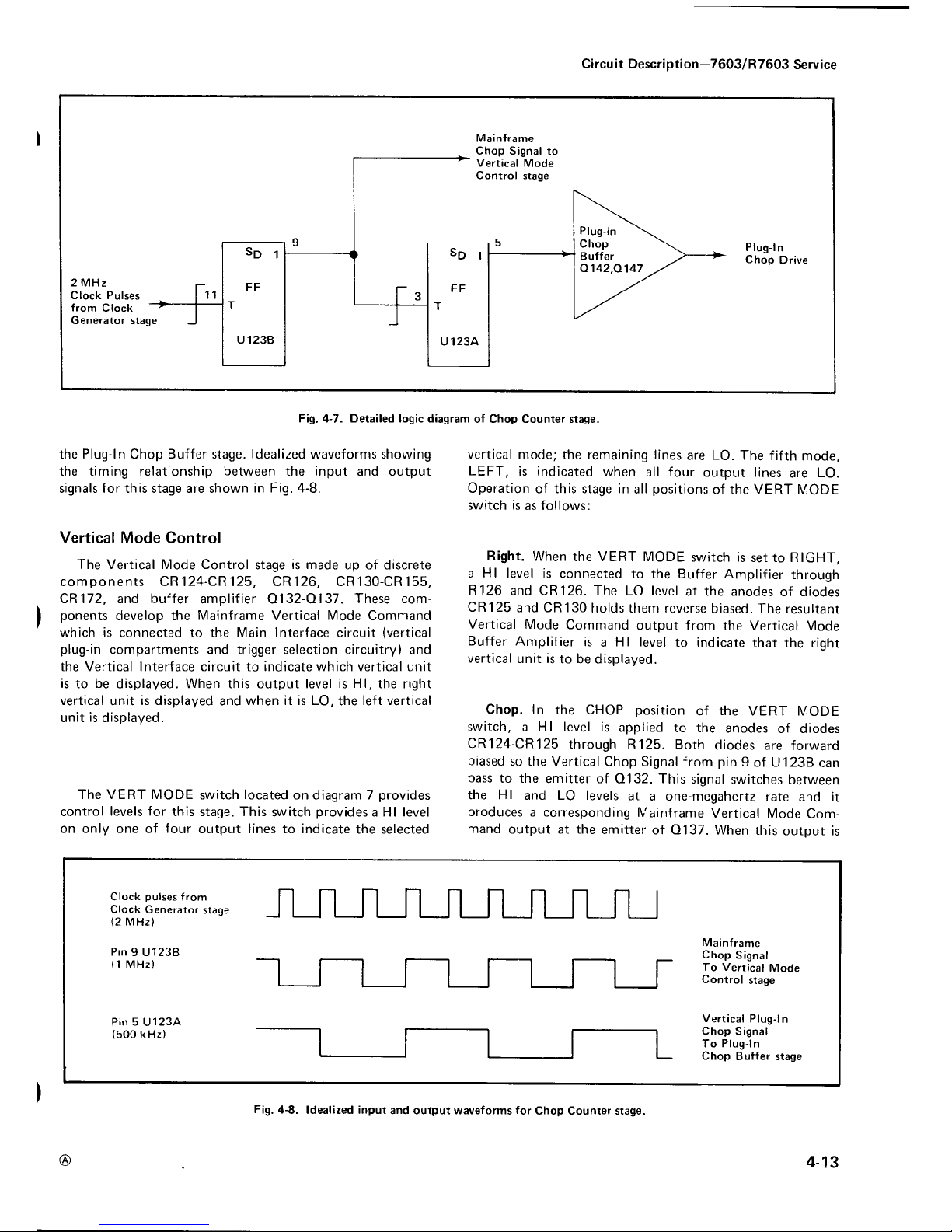
Circu it Descri
ption-7603/R7603
Service
Mainf rame
Chop Signal to
Vertical Mode
Control
stage
Plug-l
n
Chop
Drive
2MHz
Clock Pulses
from
Clock
Generator stage
o142.O147
FiS,4-7. Detailed logic diagram
of Chop Counter stage.
the
Plug-ln Chop Buffer stage. ldealized
waveforms showing
the timing relationship
between
the
input
and output
signals for this stage are shown
in Fig. 4-8.
Vertical Mode
Gontrol
The Vertical Mode Control
stage
is made
up of discrete
components CR124-CR125, CR126, CR130-CR155,
CR172,
and
buffer
amplifier 0132-0137.
These com-
ponents
develop the
Mainframe
Vertical Mode Command
which
is connected to the Main Interface
circuit
(vertical
plug-in
compartments and trigger selection circuitry)
and
the Vertical Inter{ace circuit to indicate which vertical unit
is
to be displayed. When this output level
is
Hl, the right
vertical
unit
is displayed
and
when it is LO,
the
left vertical
unit
is
displayed.
The VERT MODE
switch
located
on
diagram
7
provides
control
levels for
this stage. This
switch
provides
a Hl level
on only one of four
output lines to indicate
the selected
vertical
mode;
the remaining lines
are
LO. The
fifth
mode,
LEFT,
is indicated
when all four
output lines
are
LO.
Operation
of this stage in
all
positions
of the VERT MODE
switch is
as follows:
Right.
When
the VERT MODE
switch is
set to RIGHT.
a Hl level is
connected
to the Buffer Amplifier
through
R126
and
CR126. The
LO level
at the anodes
of
diodes
CR125
and CR130
holds them reverse
biased.
The resultant
Vertical Mode
Command
output from
the Vertical
Mode
Buffer
Amplif ier
is a H I level
to ind icate
that the right
vertical
unit is
to be displayed.
Chop.
In
the CHOP
position
of
the
VERT MODE
switch, a H I
level is
applied
to the
anodes
of diodes
CR124-CR125
through R125. Both
diodes are
forward
biased
so
the Vertical
Chop Signal from
pin
9
of U1238
can
pass
to the
emitter of
O132.
This
signal
switches
between
the H
I
and LO levels
at
a one-megahertz
rate and it
produces
a
corresponding
Nlainframe
Vertical Mode
Com-
mand
output at the
emitter
of O137. When
this
output is
Clock
pulses
from
Clock
Generator
stage
(2
MHz)
Pin
9 U1238
(1
MHz)
Pin 5
U'123A
(500
kHz)
Mainf
rame
Chop
Signal
To Vertical
Mode
Control
stage
Vertical
Plug-ln
Chop
Signal
To Plug-ln
Chop
Buffer stage
@
Fi9.
4-8.
ldealized input
and output waveforms
for
Chop Counter stage.
4-13
Page 60

Circu it Descri
ption
-7603/R
7603
Service
Hl,
the right
vertical
unit is
displayed
and
when it
switches
to LO,
the left
vertical
unit is
displayed.
Alt.
In
the ALT
mode,
the VERT
MODE
switch
applies
a Hl
level
to the
anodes
of diodes
CR130-CR1b5
through
R
130. These
diodes
are forward
biased
so
the Display
Right
Command
from
pin
5
of U156,4
can
pass
to
the
emitter
of
O132
to
determine
the Mainframe
Vertical
Mode
Command
level.
The
Display
Right
Command
switches
between
its Hl
and LO
levels
at a rate
determined
by
the Vertical
Binarv
stage.
Add
and Left.
The
control
levels
in
the
ADD
and
LEFT
positions
of the
VERT MODE
switch
are not
connected
to
this
stage.
However,
since
only
the line
corresponding
to
the
selected
vertical
mode
can be
Hl,
the
RIGHT,
CHOP.
and ALT
lines
must
remain
at their
LO level
when
either
LEFT
or ADD
are selected.
Therefore,
the emitter
of e132
remains
LO
to
produce
a LO Mainframe
Vertical
Mode
Control
output level.
Final
control
of
LEFT
or
ADD
mode
is
made
by
the Vertical
Interface
circuit.
A
logic
diagram
of the Vertical
Mode
Control
stage is
shown
in
Fig.
4-9.
The
discrete
components
which
make
up
each logic
function
are identified.
The gate
connected
to
the input
of the Vertical
Mode
Buffer
Amolifier
is
a
phantom-OR
gate.
A
phantom-OR
gate performs
the
OR
logic
function
merely
by
interconnection
of the
three
inouts.
Vertical
Binary
The
Vertical
Binary
stage
consists
of integrated
circuit
U1564
and transistor
0150.
U1564
is
a D-type
flip-flop
with
direct-set
and direct-clear
inputs
(see
Table
4-1
for
operating
details).
The
connection
between
the
,,0,,
outout
and
the
data
(D)
input
enables
this flip-flop
to
operate
in
the triggered
mode. A
logic
diagram
of the Vertical
Binary
stage
is shown
in
Fig. 4-10.
The
operation
of the
Vertical
Binary
stage
is
controlled
by
the level
of the ALT
Mode
line
from
rhe
VERT
MODE
switch.
When
this
switch is
set
to
ALT,
a Hl
level is
connected
to
the
emitter
of 0150
through
R152.
This
Hl
level
disables
O150
so its
collector
remains
Hl.
As
a result,
O150
has
no
effect
upon
operation
of the
Vertical
Binary
stage
and
the direct-clear
input
of
U1564
remains
Hl
so it
does not
affect
the operation
of
U 1 564. Therefore.
U 1 56,4
operates
as a basic
triggered
f
lip-flop
which
changes
output
states
with
each
positive-going
Sweep
Holdoff
pulse
at the
trigger
(T)
input.
The
Sweep
Holdoff pulse
goes positive
at
the
end
of each sweep.
The
signal
at the,,l,,output
of
U1564
switches
between
the Hl
and LO
level
at one-half
the
rate
of the
Sweep
Holdoff
signal
from
the
horizontal
plug-in
unit. Fig.
4-1
1 shows
the
time relationship
between
the input
and output
signals
for
this
stage,
and
gives
the
resultant
display
with
each
signal
combination^
For
any
other
position,
the
emitter
of O150
is
pulled
LO
by
the ALT
Mode
command
from
the
VERT
MODE
switch.
This
enables
O150, but
it
does
not
change
output
state
unless
the level
at the
"1"
output
of
U156A is Hl.
Ouiescently,
the
output
of O150
is
LO.
Therefore,
when
the
positive-going
Sweep Hold-off
pulse
is received
at the
end
of the sweep,
the
"1"
output
of U1b6A goes
Hl.
This
activates
O150
and its
output
goes
LO
to
provide
a
direct-clear
reset
to
U1564. The
"1"
output
of
U1564 is
reset
to its
LO level,
and O150
is
again
disabled
so its
output returns
to the Hl
level.
The
stage
is now
ready
for
From
VERT
MODE
switch
RIGHT
Mode
CHOP
Mode
ALT
Mode
Vertical
Chop Signal
from
Pin
9, Ul23B
Mainframe
Vertical
Mode
Command
Display Right
Command
from
Pin 5, U1564
or 0173
Vertical
Mode
Buffer
Amplif
ier
o132
o137
cR124
cR125
cR130
cR155
cR172
4-14
Fig.
4-9.
Logic diagram
of
Vertical
Mode
Control
and Vertical
Mode
Buffer
Amptifier
stages.
@
Page 61

Circu
it Description-7603/R7603
Service
input.
Therefore,
this
stage
is
now
operating
as a divide-by-
one counter rather
than a divide-by-two
counter
as
described
previously.
The
output under
this condition
is
used
only by the Plug-ln
Binary
stage.
Since
the
Vertical Binary
stage can change
output states
only at the end of each sweep, there will be
no Alternate
Drive
signal
for
either the
mainframe
or
vertical
plug-in
units if a sweep is not being
produced
by
the horizontal
plug-in
unit.
Plug-ln
Binary
The
Plug-ln Binary stage consists
of U1568, which is
connected
as a triggered flip-flop with direct-set input.
The
trigger input for this
stage
is
the Display Right
Command
from
the Vertical Binary
stage. When the VERT MODE
switch is set to ALT, the repetition
rate
of
the Display
Channel
2 Command
output of this stage is
one-fourth of
the Sweep Holdoff input
(see
waveforms in Fig.4-11).
For
any
position
of the
VERT MODE
switch
except
ALT,
the
repetition
rate
of
the
output
signal
from this stage is
one-half of the
Sweep Holdoff input. A
logic
diagram of the
Plug-ln Binary
stage
is
shown
in
Fig.
4-12.
Fig. 4-10. Logic diagram of Vertical Binary stage.
the next
positive-going
Sweep Hold-off
pulse.
The action is
the
same
with each
pulse,
so the signal at the output of this
stage
is
at the same repetition rate
as
the
Sweep
Holdoff
I
7
I
End of
I
Sweep
i
Start ol
Sweep
Sweep sawtooth
Sweep Holdoff
from
Time'base
Unit
Display Right Command
Vertical Einary Stage
Output
Display
Channel
2
Command
Plug-ln
Binary
Stage Output
Display
when
using
two
dual-trace
vertical units in
ALT mode
Right
Vert
ica I
Unit
cH2
Left
Vert ica
I
Unit
CH1
Fig.
4-1 1. ldealized
waveforms showing relationshap
between input
and output waveforms for
Vertical
Binary and Plug-ln
Binary stages
when
operating in
ALT mode.
@
4-15
Page 62

Circuit
Description-7603/R7603
Service
Plug-l n
A lternate
B
uffer
o162
o167
SDt
FF
T
Plug-ln
Binary
U 1568
Plug-l
n
A
lternate
Command
D isplay
R ight
Com ma nd
Fig.4-12.
Logicdiagramof
Plug-lnBinaryandPlug-lnAlternateBufferstages.
Output
Buffers
The
output
switching
commands
from
the Logic
circuit
are
provided
through
buffer
stages
Q142-0137,
4142-A147,
o-162-A167,
and 0182-0187.
Each
of these
stages
includes
a common-base
input
transistor
to
provide
a
low-impedance
load
for the
associated
driving
stages. The
output transistor
is connected
as
an
emitter-follower
to
provide
isolation
between
the
Logic
circuit
and other
circuits
within
this
instrument
or the
plug-in
units.
TRIGGER
SELECTOR
The Trigger
source
switch determines
which
vertical
signal
is connected
to the time-base
unit, and which
vertical
signal,
that is
provided
at VERT
SIG/OUT
connecror
on
the rear
panel.
Fig. 4-i3
shows a detailed
block
diagram
of
the
Trigger
Selector
circuit, along
with
a simplif
ied diagram
of
all the
circuitry involved
in
selection
of the
trigger
source.
A schematic
of the
Trigger
Selector
circuit is
shown
on diagram
3
at the rear
of this
manual.
Also,
see diagrams
6
and 7 for
the signal
selection
circuitrv not
shown
on
diagram
3.
Trigger
Mode
and Add
Signals
General.
The
circuitry
shown
on the left
side
of the
simplif
ied
diagram in Fig. 4-13
determines
the operation
of
the Trigger
Channel
Switch stage.
TRIG
SOURCE
switch
S1011
controls Trigger Channel
Switch
U324 through
O314. When
the TRIG SOURCE
switch is
set
to the VERT
MODE
position,
the
setting of the
VERT MODE
switch
determines the
trigger selection. In
the LEFT
or
RIGHT
positions,
the trigger
signal
is
obtained from
the
indicated
vertical unit. The
following
discussions
give
detailed
opera-
tion
in
each
position
of the TR lG
SOURCE
switch.
Vert
Mode. In
the VERT
SOURCE
switch,
the setting
determines
the
operation o{
stage. In
the LEFT
position
4-16
MODE
position
of the
TRIG
of the VERT MODE
switch
the Trigger
Channel
Switch
of
the
VERT
MODE
switch.
the base
of O314 is
connected
to
ground
through
the ALT
and RIGHT
sections
of 5102
1, CR102
1
and CR1026,
and
51011.
This
holds
0314
reverse
biased
to
provide
a
LO
level
to
pin
4
of
U324
(see
Fig.
4-141
.
When
the
VERT MODE
switch
is
set
to
ALT.
+b
volts is
applied
to
the
base
of 0314 through
CR
1021
and 51011.
0314 is
forward
biased
and its
emitter
level
is
determined
by
the Mainframe
Vertical
Mode
Command
signal
from
the
Logic
circuit
applied to its
collector.
This
signal switches
between
the Hl level
(Right
Vertical
unit to be
displayed)
and the
LO level
(Left
Vertical
unit
to be
displayed)
atthe
end
of each sweep.
When
the Mainframe
Vertical
Mode
Command
is Hl,
it
provides
a
positive
collector
voltage
to
O3i4.
0314 is
saturated
due to
CR1021,
and its
emitter
level
is
very
near
the collector
level.
This
provides
a Hl
output level
to the Trigger
Channel
Switch
stage. As
the
Mainframe
Vertical Mode
Command goes
LO,
the collector
supply
for Q314
also
goes
negative.
0314 remains
saturated
and
the
output
again follows
the collector
level
to supply
a
LO
output
level
to U324.
For ADD
and CHOP
vertical
mode
operation,
+g
ye11,
It
connected
to
pin
14
oI U324 through
CR1023
or CR1024
and S1011. At
the same
time, the
base
of
0314
is
held
LO
by
the
ground
connection
through
the ALT
and RIGHT
section
of 51021 so
the level
at
pin
4
of
1J324
is LO
also
(produces
an
ADD
mode in Trigger
Channel
Switch;
see
description
of this
circuit
which
follows).
In
the RIGHT
position
of the VERT
IMODE
switch,
+5
volts
is connected
to the base
of O314 through
CR1026
and S101 1
to
forward-bias
the transistor.
The
Mainframe
Vertical
Mode
Command
signal connected
to the
collector
of 0314 is
also
Hl
in
this mode,
and a
Hl
output level
is
produced
at the
emitter
of
O314.
Left.
When
the LEFT
trigger
source
is selected,
the
VERT
IVIODE
switch is
disconnected
from
the
trigger
selector
circuitry.
Now
the
ground
connection
through
the
@
Page 63

so
F3
oo
E5
33
oil
J@
I
I
I
I
I
I
v
I
I
I
I
lo
:
io
=;
c:
O;
c-
-c
oL
Er
3:
J6
o
o
o
€
EE
6E
oo
!o
o
+
I
-l
I
F
I
E
I
I
FU
tro
ilo
-e
GE
o- Y A
BE:
E
i 3f3
\--v=J
E
3.9
;i'i i
a>c
!
Y:
>l
s
i'
"l
to
I
t_
!
F
tt
UJ
J
+N
.(oN
lNo
l=E
o5
to
+
lst
IN
lo
6E
to
+
tx
tF
vi
to
+
IT
tF
.\t
$
+
I
I
P
J
F
I,
=l
Ol
-r-
al
F,
F
I
U
J
ob
Er;
F<
o
.9^PcS
Ci rcu it
Description-7603/R
7603
Service
@
4-17
Fig.tt-13.
Detailedblockdiagramof
TriggerSelectorcircuitalongwithsimplifieddiagramof
triggersourceselectioncircuitry.
Page 64

Circuit
Description-7603/R7603
Service
'Pin
14 LO
for
all other conditions.
Fig.4-14.
Input levels
at
pin
4
of U324
(source
of triggering is
shown in
parenthesis).
RIGHT
section
of S1011 establishes
a
LO
output level
at
the
emitter
of
0314.
Right.
In the RIGHT
position
of the TRIG
SOURCE
switch,
+5
volts is connected
to the
emitter
of 0314
through S'101 1
and R312. This
produces
a
H I
output level
to
the
Trigger
Channel
Switch stage.
Trigger Channel
Switch
The
Trigger
Channel
Switch stage
determines
which
input
signal
provides
the
trigger signal
to the
horizontal
compartment
as controlled
by
the
Trigger
Mode
and
ADD
signals
from
the trigger selection
circuitry.
Refer
to diagram
3
during the following
discussion.
Resistors
R317 R319
establish
the input
resistance
and
provide
a
load
for the
trigger signal
from
the right vertical
plug-in
unit.
Resistors R307
and R308,
provide
the input
resistance
and load for
the left
vertical
plug-in
unit.
R321-R323"R324
and
R326 R327-R328 establish
the
oper-
ating level
of the Trigger
Channel
Switch; R321-R323
and
R326-R328
set the current
gain
for
each
channel.
This
stage
is made up
primarily
of integrated
circuit
U324. An
input/output
table
for
U324 is
shown in
Fig.415.
U324
provides
a
high
impedance
differential
input for
the
trigger
signal from
the left vertical
unit
at
pins
2
and 15,
and
for
4-',8
the trigger signal from
the
right
vertical
unit at
pins
7
and
10. The
output signal at
pins
12
and 13 is a differential
signal. The sum
of the DC current
at
pins
12
and 13 is
always
equal
to the sum of the
DC currents
at
pins
1, 8,9,
and
16 in
all
modes.
This
provides
a
constant
DC
bias
to the
stages which
follow
as the TRIG
SOURCE
or the VERT
MODE
switches
are changed.
When
the
level
at
pin
4
is LO
(see
Trigger
Mode
and
ADD
Signals
discussion
and
Fig.
4-15),
the
trigger
signal
from
the left
vertical
unit
passes
to
the
output, while
the
trigger
signal
from the
right vertical
unit is
blocked.
A
Hl
level
at
pin
4
connects
the trigger
signal
from
the right
vertical
unit to
the output
and the
trigger
signal
from
the
left
vertical
unit is
blocked. For
VERT
MODE
ooeration in
the
ALT
position
of
the
VERT MODE
switch,
the level
at
pin
4
switches
between
the LO
and Hl
level
at
a rate
determined
by
the Vertical
Binary
stage
(see
Logic
circuit
description).
This
action
obtains
the trigger
signal
from
the
left
vertical
unit when
the left
vertical
unit is
being
displayed
and from
the
right
vertical
unit when it is
being
d
isplayed
.
When
the level
at
pin
4 is
LO
and
the level
at
pin
14 is
Hl,
the
trigger
signal from
both
the left
and right vertical
units
passes
to the
output
pins.
This
condition
occurs
only
when
the TR lG
SOURCE
switch is
set
to VERT
MODE
and
the VERT
MODE
switch is
set
to
either ADD
or CHOP.
Under
this
operating mode,
the trigger
output
signal is
the
algebraic
sum
of the trigger input
signals
from
the left
and
right
vertical
units to
prevent
triggering
on the
vertical
chopping
transition,
or only
on
one signal
of an added
display.
Trigger
Output
Amplifier
The
trigger
output
at
pins
12
and
13
of U324 is
connected
to the bases
of 0344
0346
to
provide
the
internal
trigger
signal for
the horizontal
unit
(via
the Main
Interface
circuit). The
horizontal
unit
provides
a 50-ohm
differential
load
for
this stage. lf
it is
removed
from its
compartment,
the
collector load
for
0344-0346
changes
and
the voltage
at their
collectors
increases.
This
stage
prevents
this change from
affecting
the vertical
signal for
the
Output
Signals
board.
CR341
CR349 clamp
the collec-
tors
of 0344 and
0346
at about
+0.6
volt
to
prevent
these
transistors from
saturating under
this no-load
condition.
Vertical
Signal
Buffer
The
trigger
output
signal
at
pin
12
and 13
of U324 is
also
connected
to
the emitter
of
a common-base
amplif ier
Q336
and
0334.
The
output signal
at the collector
of e336
and 0334 is
connected
to
the siqnals
out
board.
VERT MODE
LO
(Left
Vertical)
Hl
(Right
Vertical)
Switches
from
LO
to Hl.
and
vico versa,
at end
of each sweep
(both;
follows
display
)
LO
at
pin
4
of
U324. Hl
at
pin
'1
4'
(both;
added
algebrai.
cally
)
@i
Page 65

VERTICAL
INTERFACE
The
Vertical
Interface
circuit selects
the vertical
def lec-
tion
signal
from the
output
of the left
vertical
and/or
the
right
vertical
plug-in
unit. Fig.
4-16
shows a detailed
block
diagram
of
this circuit
manual.
Vertical
Channel
Switch
The
Vertical
Channel
Switch
stage
determines
which
input
signal
provides
the vertical
signal
to the
Delay-Line
Driver
stage
as controlled
by
the Mainframe
Vertical
Mode
Command
from
the Logic
circuit.
Resistors
R200-R202
and
R204-R206
establish the input
resistance
of this
stage
and
provide
a
load
for
the left
and right
vertical
units.
Resistors
R209
R211-R212
and
R216-R218-R219
estabtish
the oDer-
ating levels
for this
stage. R209-R212
and R216-R219
set
the
current
gain
for
each
channel.
C208-R208
and
C215-R215 provide
f requency
compensation.
This
stage is
made
up
primarily
of integrated
circuit
U214,
which is
the same
type
as used
for
the Trigger
Channel
Switch. An
input/output
table for
U2l4 is
shown
in
Fig. 4-17.
U214
provides
a
high
impedance
differential
input
for the
signal
from
the left
vertical
unit
at
pins
2
and
15,
and
the signal
from
the right
vertical
unit
at
pins
7
and
10.
The
output signal
at
pins
12
and 13 is
a differential
signal
which is
connected
to the
Delay-Line
Driver
stage
through
R222-R224.
The
sum
of the DC
outpur
currents
at
Circu it
Description
-7603/R
7603
Service
Vertical
Interface
circuit.
A
schematic
of
shown
on diagram
3
at the
rear
of this
the
is
Input
Output
/f
f/
//
/"e
/
^.8
/
rrieser
output
Sisnal
14
112,13
LO
LO
Left trigger
signal
HI
LO
Right
trigger
signal
LO
HI
Both
(added
algebraicallyl
Fig.4-15.
Input/output
table
for
Trigger
Channel
Switch
stage
X/Y
Shutdown
Readout
Mainframe
Vertical
Mode
Command
from
Logic
circuit
ADD
Mode {rom
VERT
MODE
switch
Left Vertical
Signal
from
Left Vertical
unit
Right
Vertical
Signal
from
Right
Vertical
unit
Vertical
Signal
to
Vertical
Amplif
ier
Auxiliary
Y-Axis lnput
from
Horizontal Plug-ln
Vertical
Channel
Switch
U214
Aux iliary
Y Axis
Input
Amplif
ier
0225.4236
@
Fig.
4-16.
Vertical
Interface
derailed
block diagram.
4-19
Page 66

fnput
I
Output
6::
/s/
,g/
"8
/
output sisnal
14
112,13
LO LO Left
vertical
signal
HI LO
Right vertical
signal
LO HI Both
(added
algebraically)
Circu it Description-7603/R7603
Service
Fig.4-17. Input/output table
for Vertical Channel Switch.
pins
12
and
13
is
always
equal to the sum of the DC
input
currents
at
pins
1,8,9, and I6
in
all modes.
This
provides
a
constant DC bias
to
the
following
stage as the
VERT
MODE
switch
is changed.
When the VERT MODE swich is set
to
LEFT, the level
at
pin
4 is LO. This level
allows the signal from the left
vertical unit
to
pass
to the
output
while
the
signal
from the
right vertical unit is
blocked.
In
the
RIGHT
position
of the
VERT MODE switch, the level at
pin
4 is Hl. Now,
the
signal
from
the
right
vertical unit
is
connected to the
output
while the signal from
the
left
vertical unit
is
blocked.
When
the
VERT MODE
switch
is
set to either ALT
or
CHOP, the Mainframe Vertical Mode
Command at
pin
4
switches between
the
LO
and
Hl levels
at a rate determined
by
either the Chop
Counter
or the Vertical Binary stages
(see
Logic circuit
description).
This
action allows the signal
from the
left
vertical unit to
be d isplayed
when the
Mainframe Vertical Mode Command is
LO and the signal
from
the right vertical unit
is
displayed when the Main-
frame Vertical Mode Command is Hl. When ADD
vertical
mode
operation
is
selected, a
Hl level is
applied to
pin
14
and the level
at
pin
4 is
LO
as determined
by
the Vertical
Mode Control
stage
in
the Logic Circuit. This
allows
both
the
right
and
left
vertical signals to
pass
to the
output
pins.
Now,
the signal from both vertical
units
is
algebraically
added
and the resultant
signal determines
the vertical
def
lect ion.
The
X/Y
Shutdown signal from
the Readout
system is
applied to
pin
6 of U214. lt has
final
control
over the
output signal from
U214. Ouiescentlv,
the X/Y
Shutdown
signal is LO
and the
signal from the
selected vertical
can
pass
to the output
pins
12
and 13. However,
when the
4-20
Readout
system is ready
to display
Readout
information,
the level
at
pin
6
goes
Hl. This
level
blocks
the signals
from
both
vertical
compartments
and
there is
no
output from
U214 under
this condition.
Transistor
0238
will conduct
and
provide
about the
same current
for
the
output stage
as
under normal
conditions.
This
limits
any change
in
posi-
tioning
that would
otherwise
occur
when
the X/Y
Shut-
down
signal from
the Readout
system is
applied.
Auxiliary Y-Axis Input
Amplifier
The
Auxiliary Y-Axis Input
Amplif ier
accepts an
input
from horizontal
plug-in
units having
compatible
features.
Normally,
this
input is
a
positioning
voltage
to
offset
the
display. The single-ended
signal connected
to the
input
of
this stage is
converted to a
push-pull
signal at the
collectors
oI Q225 and 0236. This
signal is connected
to
the
Delay-Line
Buffer stage along with
the
output from the
Vertical
Channel Switch.
Delay-Line
Buffer
The
output
of
the
Vertical Channel
Switch stage,
along
with
any signal from
the
Auxiliary
Y-Axis
Input
Amplifier,
is
connected
to the
emitters of Q242-A252.
These
tran-
sistors
are connected as common-base
amplif
iers
to
provide
a low-impedance
current-summing
point.
The
signal
at the
collectors
of Q242-Q252 is
connected
to
Delay Line
/
DL400.
Resistor R260
provides
reverse
termination for
the
I
Delay Line.
Delay Line
Delay
Line
DL400
provides
approximately
150
nano-
seconds
delay for the vertical signal,
to allow the horizontal
circuits
time to
initiate
a
sweep before
the vertical
signal
reaches the vertical
deflection
plates
of the CRT. This
allows the
instrument
to
display the leading
edge
of
the
signal
originating the trigger
pulse
when using internal
triggering. The
delay
line
used in this instrument
has
a
characteristic impedance
of about 50
ohms
per
side,
or
about
100
ohms differentially. lt is
of the coaxial type,
which does not
produce preshoot
or
phase
distortion in
the
CRT display.
VERTICAL
AMPLIFIER
The
Vertical
Amplif ier
circuit
provides
final
amplifica-
tion
for the vertical
signal before it
is
applied
to the vertical
deflection
plates
of the
CRT. This
circuit includes
an
input
from
the BEAM
FINDER
switch
to compress
an over-
scanned
display within the
viewing
area
of the CRT. Fig.
4-18
shows
a detailed block
diagram
of the Vertical
Amplifier
circuit. A
schematic of this
circuit is
shown
on
diagram
4
at the rear of this manual.
@
Page 67

J409
Vertical
Readout
Signal
Vertical
Signal
from
Delay
Line
Vertical
Def lection
Signal to
vert
ical
deflection
plates
on
C
Limit Command
from
BEAM
FINDER
switch
Display
Limited
Current
to Horizontal
Amplifier
Fig. 4-18.
Vertical
Amplifier
detailed block diagram.
Input
Balance
Q407 0415 comprise
a
paraphase
amplif
ier
to
provide
input
balance for
the Vertical Amplifier
by changing the
DC levels
at
pins
2
and 4 of U450.
Vertical Centering
adiustment R403
determines
the
bias
at the base
of 0407.
As
this bias is
changed, the levels
at
the
collectors
of
Q407
and 0415 change
due to
paraphase
action.
This
DC level is
connected
to
pin
2
of U450 through R408-R423
and to
pin
4
through
R414-R424.
R403 is
adjusted so the
trace
is
displayed
at
the
center of
the CRT when the inputs
to this
circuit are
at the same
potential.
The input
to the base
of 0407 through
J409
is
used for
Vertical
readout sional.
Output Amplifier
Amplification
of the vertical
signal is
accomplished by
integrated
circuit U450. The
circuit
shown within
the
shaded
area
is
a representation
of the circuit
contained
within U450. Notice
that the circuit is
made up
of three
similar
push-pull
stages. Each
stage has
a
pair
of common
emitter transistors
driving a
pair
of
low input
impedance
common
base transistors. Frequency
compensation
is
pro-
vided
by
the
networks
connected between
pins
2
and 4 in
the first
amplifier stage
and
pins
7
and
8,
13 and 14 in
the
@I
Circuit Description
-7603/R
7603
Service
third
amplifier stage. The
resistive network
connected
to
pins
3,
6, and 16 determines
the
gain
of
the Vertical
Amplif
ier. Vertical
Gain
adjustment R447 sets
the
gain
of
the second
amplifier stage to
determine the
overall
gain
of
the vertical
deflection system
and thereby
provide
a
calibrated
deflection
factor.
Bias adjustment
R486 sets
the
voltage level
at
pin
10
of U450
(nominally
4.3
volts) to
balance
the third
amplifier stage for
maximum
gain-
bandwidth
ooeration.
Beam Finder
Network
The Beam Finder
Network, consisting
of transistor 0496
and
associated components,
provides
a means
of
locating
a
display which
overscans the
graticule
area. Under
normal
operation,
-15
volts is connected
to the
base
of 0496 from
the
BEAM FINDER
switch
(see
diagram 7)
to
reverse
bias
it.
Therefore,
the normal
operating levels for
U450
are
determined by the resistive network
connected
to
pins
3,
6,
and 16. When
the BEAM FINDER
switch is
pressed,
the
-15
volts is interrupted
and the base
of 0496 rises
positive
to turn it
on.
The
resulting change in
current
of U450
unbalances
the second
amplifier stage so
as to
limit
its
gain.
This
action compresses the
display verticallV
within
the
display
area.
HORIZONTAL
AMPLIFIER
The
Horizontal Amplif ier
circuit
amplif
ies
the
push-pull
horizontal
deflection signals from
the
plug-in
unit in
the
horizontal
compartment
and
connects
it
to the horizontal
def
lection
plates
of the CRT. Fig. 4-19
shows
a detailed
block
diagram of the Horizontal
Amplifier circuit.
A
schematic
of this circuit is shown
on diaqram
5 at the rear
of
this manual.
Horizontal
Channel
Switch
The
horizontal
signals from
the
plug-in
unit in
the
horizontal
compartment
are connected
to
pin
2
and
pin
15
of U510.
The Readout
signal is
connected
to
pin
7
of
U510. Integrated
circuit
U510
determines
which input
signal
will
provide
the
signal for
the Horizontal
amplifier
circuit
as controlled by
the X/Y
Shutdown
signal
from the
Readout
system. When the X/Y
Shutdown is LO, the
signal
from
horizontal
compartment is
passed
to the
output of
U510. When
the
X/Y
Shutdown is high, the Readout
signal
is
passed
to the output
of U510. Resistors
R514, R51S.
R521, and
R522
establish
the
operating
levels for
this
circuit.
R512
adjusts the circuit
gain.
R51 1
and
R513
establish
the range for
the
gain
adjustment
(see
Trigger
Channel
Switch under TRIGGER
SELECTOR
in
this
section
)
.
For normal operation, the
gain
and current level resistors
are
connected
to the Display Limit
Command line.
The
4-21
Page 68

Circuit
Description
-7603/R7603
Service
Right
Outpul
Amplif
ier
0539.
O551
0558,
Os60
Left
Output
Amplif
ier
o553.
0547
0578.
0580
Display
Limited
Current from
Vertical
Amplifier
Horizontal
deflection
signal
to right
deflection plate
of
CRT
Horizontal
signal from
horizontal
plug-in
compartmenl
Horizontal
Readout
Signal
Display
Limit Command
from
BEAM
FINDER
switch
Horizontal
deflection
signal
to left
deflection
plate
of
CRT
I
Fig.
4-19.
Horizontal
Amplif ier
detaited
block
diagram.
Display
Limit
Command
is
connected
to the
-15
supply
through
the
BEAM F
lN
DE R
switch.
When
the
BEAM
FINDER
switch is
actuated,
the
'l
5
volt
is
interrupted
to
limit
the
current
to
U510.
At the
same
time,
current
is
added
through
CR531
and
CR532
from
the display
limited
current
line.
This
added
current
maintains
about
the
same
DC currents
through
the
output
circuit
in
both
positions
of
the
BEAM
FINDER
switch.
The
signal
at
the
ourpur
rs
connected
to
the right
and left
amplifier
inputs.
Resistor
R525
adjusts
the
amplifier
for
center
screen
deflection
in
the
absence
of
an input
signal
to
U510.
Output
Amplifier
Transistors
0539,
O551,
O5SB,
and
eb60 f
unctron
as
a
current
driven
feedback
amplifier.
The input
current
is
converted
to a voltage
output
signal
to
drive
the right
horizontal
CRT
deflection
plate.
R5bg
establishes
the
quiescent
current
level for
series
connected
transistors
0558
and 0560
The
CRT
def lection
plates
present
a capacitive
load
to
the
amplifier,
which
requires
additional
current
during
fast
transients.
Extra
current
for
positive
excursions
is
provided
4-22
by 0551
via
R555,
C555, and
0558; for
negatrve
excur.
sions, by 0560
via
R563.
Resistor
R556
reduces
the
power
dissipation
in
O5b8.
Resistors
R566,
R567,
and R569
provide
DC
feedback
and
establish
low
frequency gain.
Capacitors
C566
and
C588
(C568
for
lower
serial numbers)
are adjusted
for
correct
gain
at
fastest
sweep rates
(in
later
serial numbered
instruments,
C588
replaces
C568
and
a differently
located
C588, a
thermal
compensation
network
C584-R584
is
added
).
Basic
operation
of
the
Left
Output
Amplif
ier
stage
is
the
same
as described
for
the
Right
Output
Amplif
ier.
C5g6
and
C588
set
the
gain
for
the fastest
sweep
rates
(Csgg
is
relocated
for
later
serial numbers
and
affects
both
Right
and
Left
Output
Amplif
iers).
The
output
signal
at
the
collectors
of 0578-O580
connects
to the
left
deflection
plate
of
the
CRT through
R585.
The
series
circuit
CR549
and
R549
stabilize
tne
output
amplifier
during fast
retrace
intervals.
R535 is
adiusted
to
balance
the negative
excursions
of the
right
and left
sides
of
the
amplifier
when
the
time base
plug-in
is
used
in
X.l0
Magnified
mode.
@
Page 69

Circuit Description-7603/R7603
Service
Output Amplif
ier
o1070. o1072
Output
Voltage
Divider
r
[;l
Fr
-rl
lcNp-l
Fig.
4-2O.
Calibrator
detailed
block
diagram.
CALIBRATOR
AND FRONT
PANEL
SWITCHING
The Calibrator
and Front
Panel
Switching
circuit
pro-
vides
output voltage
to the
front-panel Calibrator
pin-iacks
and
includes
the
front-panel switches
and controls.
Fig.
4
2O
shows
a
detailed
block
diagram of
the Calibrator
portion
of
this circuit.
A schematic
of
this circuit
is shown
on
diagram 7 at
the
rear of this
manual.
Mode
Switch
Logic
The
VERT
MODE switch determines
the operating
mode of
the
Vertical Interf ace
circuit. The
levels
established
by this switch are also
used
in various other
circuits
throughout
this
instrument. This switch
is designed
so
it is self-cancelling
(i.e.,
only one
button
can be
pressed
at a
time). Specific operation
of
this switch
is described
in
connection
with the
circuits that
it controls.
The TRIG
SOURCE switch
controls the operation
of
the
Trigger Selector
circuit.
This switch
is
also
self
-cancelling
so
only one
of the
buttons can
be
pressed
at a
time.
Operatiorr
of this
switch
is
discr.rssed
in
connectiotr
with
the
Trigger
Selector
circuit.
Calibrator
General.
The Calibrator
circuit
provides
accurate
voltage
output at
the
front'panel
Calibrator
pin'iacks.
Repetition
rate of
the output
signal
is about one
kilohertz.
Oscillator. O106i
and
O1066 are connected as a square-
wave oscillator
to determine
the
repetition rate of the
Calibrator circr.rit. Oscillation
occurs as follows:
Assume
that O106'l
is
conducting
and O1066
is
off.
The
collector
current of O1061 through
R 106'l
produces
a
voltage level
which
holds the
base
of
O'l
066 low.
This
keeps O1066
turned off, and
since there
is
no current through
it, its
collector
goes
positive
to
produce
the
positive portion
of
the
square wave.
At the same time, C1064
begins to charge
toward
-15
volts
through
R1069. The
emitter
of O1066
goes
negative
also
as C1064
charges, until
it reaches
a
level
about
0.6 volt
more negative than the
level
at
its
base.
Then, O1066
is forward
biased
and
its
emitter
rapidly rises
positive.
Since Ci064
cannot change
its
charge
instan
taneously,
the sudden
change
in
voltage at
the emitter of
O1066
pulls
the emitter
of O106
1
positive
also,
to reverse
bias
it. The
current
through O1066
produces
a voltage drop
at
its collector to
produce
the
negative
portion
of
the
square wave.
Now, conditions are
reversed.
Since
O1061
is reverse
biased, there
is no current through
it. Therefore, C1064
can
begin to
discharge
through R 1063"
The emitter level of
O1061 follows
the discharge of
C1064 until
it
reaches
about
-0.6
volt.
Then, O1061
is forward biased and
its
collector
drops
negative to
reverse bias O1066.
This
interrupts the current through
O1066, and
its collector
goes
positive
again
to complete
the square wave. Once
again,
C1064 begins
to charge through
R1069 to start the
second
cycle. The signal
produced
at
the collector of
O1066 has a
repetition
rate
of about one
kilohertz.
The Oscillator
stage
can
be
changed
by
jumper
P1066'
When
this
jumper
is installed
in
the DC
position, the
Oscillator
is disabled
and
the
collector
of O1066
rises
posi-
tive.
This
produces
a
positive
DC
voltage
output
to
the
f
ront-panel
Calibrator
pin-jacks.
Output
Amplifier.
Transistors
Q1070 and
O1072 are
connected as a
comparator
with the reference
level
at
the
base
of Qlolz
determined
by
the
network R1073 R1074-
R1076 R1O1l .
The
4 Volts
adjustment
R1O17,
is
set to
provide
accurate
output
voltage
at
the 4 V Calibrator
oin-iack.
4-23
Page 70

Circuit
Description-7603/R7603
Service
The
output of the
Oscillator stage is
connected to
the
base
of O1070. This signal
controls the
conduction
of
comparator
O1070 O1072. When
the base
of O1070 is
high, it is
off and
41072
is
conducting.
Thrs
produces
a
positive
output voltage
at the Calibrator
pin,lacks.
When
the level
at the base
of Q1070
is
switched low,
O1070
conducts
and
O1072
is
reverse biased.
Now,
the voltage
level
at the Calibrator
pin-jacks
drops to
zero.
Output
Voltage
Divider. The
collector
current
of O1072
in
the
Output
Amplif ier
stage is
applied
across the voltage
divider made up
of
resistors R
1079
through R
1085. This
divider
is
designed to
provide
a
low
output resistance
in
the
40 mV
arrd 0.4 V
positions
while
providing
accurate outpur
voltages. The
output resistance
at the 4
V
pin,iack
is
about
450
ohms and at the 0.4 V
and 40 mV
pin-iacks
is
about 50
ohms.
CRT
CIRCUIT
The
CRT Circuit
produces
the
high-voltage
potentials
and
provides
the control
circuits necessary
for
the
opera-
tion
of the cathode-ray
tube
(CRT).
This
circuit
also
includes
the Z-Axis
Amplif ier
stage
to
set the intensity
of
the
CRT display
and
the
Auto
Focus
amplif
ier
ro assure
R1139
o1110
o1',l 18
o1128
01136
41132
01134
Z-Axis
Amplif ier
o1154.
O11
Control-G r id
DC Restorer
o1 148
o1 156
Focus
Grid
DC Restorer
Z-Axis
Signal
from Beadout
Circuit
Z-Axis Signal
from Z-Axis
Logic
+15
VOLTS from
Low
Voltage
Power
Supply
R1108
H igh-Voltage
Oscillator
a1216, 01214
r 1225
H igh-Voltage
Supply
u1230
cR1232
H
Vol
R
egulator
4120
o1
121
R1045
FOCUS
-2.975
kV
Fig.
4-21, CRT Circuit detailed
block diagram.
4-24
REV.
MAR 1974
to,
I
Page 71

optimum
focus. Fig.
4-21
shows
a detailed
block
diagram
of
the
CRT Circuit. A
schematic
of this
circuit is
shown
on
diagram
8
at the
rear
of this manual.
Z-Axis Amplifier
The
Z-Axis signal
from
the Logic
circuit
and the
Z-Axis
signal
from
the
Readout system
are
connected
to the
em
itter
of O1 107.
Transistor
O1 107
is a common-oase
amplif ier
to
establish
a
low
input
impedance for
the
input
signals.
Transistors O1148,
A1152,
O1 154,
and Oi
156
form
a current driven
operational amplifier.
The input
and
output transistors
are complementary
to
provide
a
fast
rise-time
and a
fast fall-time
response.
The amplif ier input
is
through
resistor
R1108. Resistor
R1152 establishes
a
low
current
in
the series connected
output
transistors.
Tran-
sistor O1 148
supplies additional
current
through
C1151
for
the
positive
transients,
and transistor
O1 156
supplies
additional
current through
C1
158
for
negative
transients.
Capacitor C1158 is adjusted for
optimum
square-wave
output,
resistors
R1158 and
R1159 along with
capacitor
C1158
form
the
feedback
network.
Zener diode
VR1142
provides
the
necessary
change
of
voltage from
the collector
of 01 107 to
the
base
of 01 156.
Auto Focus
Amplifier
The voltage
developed
across
R i 108 by
the
Z-Axis
amplif ier
driving
current
is inverted
and
amplif ied
non-
linearly by
01 110
and
(-)1
118,
to conform
to the require-
ments
of the
CRT
focus
etectrode.
As
the base
of Q1 110
is
driven negative
CR1115 is
forward
biased,
producing
a knee
in
the
amplif
ier
response.
The
Level
where
the knee
occurs
is determined
by
the adjustment
R1121
. The operation
of
the remaining
amp[if ier is
identical
to
the Z,Axis
amplif ier.
H
igh-Voltage Oscil lator
Power for
operation of
the high-voltage
supply
is
provided
from the
+15-Volt
Supply. At
the time of turn-on,
CR 1215 is reversed biased holding the collector
of A1214
positive.
This
allows the starting base bias current for the
High-Voltage
Oscillator
to be supplied from
the
+5-Volt
Supply through
R1214,
Q1214, and the base feedback
windings of
T1225
while the emitter
potential
of
O1216-01218 is
established
by
the negative side
of
the
+15-Volt
Supply. As
the output of the high-voltage supply
increases
to its required
output
level,
the collector
of
Q1214
goes
negative
until CR 1215
is
forward
biased.
Then
the
collector level
of 01214 is
clamped about 0.6
volt more
negative
than the negative side of the
+15-Volt
Supply. This
configuration
provides
a
controlled
starting current for the
High-Voltage
Oscillator at
turn-on,
and at the same time
allows the High'Voltage Regulator stage to
cont[ol the
G)
Circu it
Description
-7
603 / R7
603
Service
current
for
the
High-Voltage
Oscillator
after
the
stage
reaches
operating
potentials
to
provide
a regulated
high_
voltage
output.
Q1216
O1218
and the
associated
circuitry
compnse
an
oscillator to
drive high-voltage
transformer
T1225.
When
the instrument
is
turned
on, assume
that
O 1216
comes into
conduction
first. The
collector
current
oI
ej2j6
produces
a corresponding
current increase
in
the
base-feedback
winding
oI T1225
to
further
increase
the conductivity
of
O1216.
At the same
time,
the voltage
developed
across
the
base-feedback
winding
connected
to
Oi216 holds
01219
reverse
biased.
As long
as the collector
current
of Q1216
continues
to
increase,
voltage is induced
into
the base-f
eedback
windings
d f 1225
which
holds
Oi216 forward
biased
and O12i8
reverse
biased.
However,
when
the
collector
current
of
O1216
stabilizes,
the magnetic
field built
up
in
T1225
begins
to
collapse. This induces
an
opposite
current
into
the
base
windings
which
reverse
biases
O1216, but
forward
biases
O1218.
When
the
induced
voltage
at the
base
of
O1218
exceeds
the bias
set by
the High-Voltage
Regulator,
O1218
conducts
and the
amplif ied
current
at
its
collector
adds
to the
current
flowing
through
T
j22S
due
to the
collapsing
f
ield.
Then,
as the
current
through I1225
stabilizes
again,
the magnetic
field
around it
once more
begins
to
collapse. This
reverses
the
conditions
ro
start
another
cycle.
The
signal
produced
across the
primary
oI f 11225 is
a
srne wave
at
a frequency
of 35 to 45
kilohertz.
The
amplitude
of the
oscillations
in
the
primary
of T'l 225 is
controlled
by the High-Voltage
Regulator
to
set
the total
accelerating
potential
for
the
CRT.
Filter
network
C1222
L1222
decouples
high
peak
operating current
from
the
+
15-Volt
Supply.
High-Voltage
Regulator
A
sample of
the secondary
voltage
from
T1
225
is
connected
to the High-Voltage
Regulator
stage
through
divider
R1245AR12458.
01201
and 01206
are
connecreo
as an
error
amplifier
to sense
any change
in
the voltage
level
at the base
of
Oi20
1.
The
ground
reference
for
the
emitter
of O'f 201
through
R12O2, establishes
the reference
level for
this
stage.
The output voltage
is
set by
the
fixed
values
of
the components
in
this circuit.
Regulation
occurs
as follows:
lf
the
output
voltage
at
the
2975V
test
point
starts
to
go positive
(less
negative),
a sample
of this
positive-going
change
is connected
to the
base
of Oi201
through
R12458.
Both
O120'l
and
O1206
4-25
Page 72

Circu it Description
-7603/R7603
Service
are
forward
biased
by this
positive
change,
which
in
turn
increases the
conduction of
O12l4.
This results in
a
greater
bias current
delivered
to the
bases
of O1216-01218
through 01214.
Now, the
bases
of
both O1216 and Q1218
are
biased closer
to their conduction
level so the feedback
voltage
induced
into
their
base-feedback
windings
produces
a
larger collector
current.
This results
in a larger induced
voltage
in
the
secondary of
f
1225 to
produce
a more
negative
level
at the
-2975
V
test
point
to correct the
original
error.
In a similar
manner, the circuit
compensates
for output
changes
in a negative direction.
Since the
amplitude of
the
voltage
induced into the secondary
of
f n25 also determines
the output
level
of
the
positive
High-Voltage Supply and
the Control-Grid Supply, the total
high-voltage output
is regulated
by
sampling
the
output
of
the
negative High-Voltage
Supply.
High-Voltage Supplies
High-voltage transformer
T
1225
has two
output
windings. One
winding
provides
f ilament voltage for the
cathode-ray
tube.
The
other
winding
provides
the
negative
and
positive
accelerating
potential
for the CRT and the bias
voltage for the
control
grid.
All
of
these voltages
are
regulated
by the
High-Voltage Regulator stage to maintain a
constant
output
voltage as
previously
described.
Positive accelerating
potential
for
the
CRT
anode is
supplied by the voltage
quadrupler
U1230. The applied
voltage
from
the secondary of f 1225 is about
six kilovolts
peak-to-peak.
This results in
an output voltage of about
+12
kilovolts at the CRT anode. The negative accelerating
potential
for
the
CRT cathode
is
also obtained from
this
same secondary winding. Half-wave rectifier
CR'l 232
pro-
vides an output
voltage of about
-2.975
kilovolts which is
connected to theCRT cathode through R1234. The
cathode
and filament
are connected together through R"1275 to
pre-
vent cathode-to-filament breakdown
due to a large dif-
ference in
potential
between these
CRT elements. A sample
of the negative
accelerating voltage is
connected
to
the High-
Voltage
Regulator
to maintain a regulated
high-voltage
ou tou t.
The network
consisting of
diodes
CR
1269-CR 1268
CR 127O'CR1264
VR1264
provides
the
negative voltage
for the
control
grid
of the CRT. Output
level
of
this
supply is set
by CRT Grid Bias adjustment
R1261.
Approximately 800 volts
peak-to-peak
from
the
secondary
of f 1225
is connected to the Control-Grid
Supply
through C1266
and R1266. Diodes CR1268
and
CR 1264 clip
this signal
to
determine
the operating
level at
the control
grid.
CR'l 268
limits
the
negative excursion of
the
signal;
quiescently
when the CRT
is blanked, the
anode
of
CR 1268
is set at about
+
15 volts by the Z-Axis
Amplif ier stage.
The
positive
clipping
level
at
the cathode
of CR1264
is set
by CRT Grid Bias adjustment
R1261.
R'l 261 is
adjusted
to
bias
the
control
grid
of the
CRT
just
4-26
enough
negative so the trace
is
blanked between
sweeps.
Under
normal conditions, this
biases the control
grid
about
80
volts more
negative than the cathode.
The negative level
at
the CRT cathode is connected to
the cathode of
CR1270.
This level is
held constant
bv
the
High-Voltage
Regulator
as
described
previously.
The
clipped
voltage developed
by diodes CR1264
and
CR1268
is
peak
to
peak
rectified
by
diodes CR1269 and
CR1270
and
super-imposed on
this negative voltage to result
in
a
level
at
the
grid
of the CRT
which is more negative than the
CRT
cathode
level.
C1269 acts as a
filter
to
provide
a
constant voltage output
level.
The
unblanking
gate
level
developed by the Z-Axis
Amplifier
stage is applied to the
anode of
CR 1268 through R 1
157. The fast rising
and
falling
portions
of this signal are
coupled
directly
to the
output
through
C1269.
The
overall effect of the unblanking
gate is
to further
clip the
negative
excursions thereby
reducing
the
voltage difference
between
grid
and cathode
of
the
CRT. This allows
the cathode current
of
the CRT
to
pass
to the anode
so the display
can be viewed.
CRT
Control Circuits
The focus
of
the
display is determined by the FOCUS
control R 1045.
This control and the
Auto
Focus
amolif
ier
maintains a well-defined display
for fast
changes in:he
intensity
of the display.
The network
consisting
of
CR 1255, CR1254, CR
1253, CR 1258,
and VR 1258
provide
the negative voltage f or the f ocus
grid
of
the CRT.
Approximately
800
volts
peak
to
peak
from
the secondary
of
f1225 is connected to the focus
grid
supply
through
C1257 and R1257. The
positive
clipping level
at the
anode
of
CR1258
is
set
by
the FOCUS
control setting.
Thii
determines
the
operating
level
at the focus
grid.
Under
normal
operating conditions
the voltage
applied
to the
focus
grid
is more
positive (less
negative)
than
the control
grid
or the cathode
of the CRT.
The signal developed
by
the Auto Focus amplifier is
coupled
to the
focus
grid
by
C1254. When there
is
a sudden change in intensity levels
the
focus
grid
level will
change to maintain
a
welldef
ined
display.
Astigmatism adjustment
R1193, which
is used
in
conjunction
with the FOCUS
control to
obtain a well-
def ined
display, varies the
positive
level
on the astigmatism
grid.
Geometry adiustment
R1184 varies the
positive
level
on the horizontal deflection-plate
shield to control
the
overall
geometry
of the
display.
Two
adjustments
control
the trace alignment
by varying
the magnetic f ield induced by
coils around the
CRT.
Y-Axis
Alignment R 1 190 controls
the current
through L1098,
which
affects the
CRT
beam
after
vertical
def lection,
but
before horizontal
deflection. Therefore,
it affects only
the
vertical
(Y)
components
of
the displaV.
Beam
Rotation
adjustment R'l
181 controls
the current through
L1099 and
affects
both
the vertical and
horizontal
rotation
of
the
display.
I
@
Page 73

LOW.VOLTAGE
POWER
SUPPLY
The Low-Voltage Power
Supply circuit
provides
the
operating
power
for this instrument
from
six
regulated
supplies. Electronic regulation
is
used to
provide
stable,
low-ripple
output voltages.
Each
supply
(except
the
+l30
V
supply,
which
is
fused)
contains
a short-protection
circuit
to
prevent
instrument
damage
if
a supply
is inadvertently
over-loaded
or shorted
to
ground.
Fig.
4-22 shows
a
detailed block
diagram
of the
Low-Voltage
Power
Supply
circuit.
A
schematic
of this circuit
is
shown
on diaqram
g
at
the rear
of
this
manual.
Power
Input
Power is
applied to
the
primary
of transformer T801
through line fuse F
1000, thermal
cutout
S1000,
and
POWER
switch
S1001.
The
Voltage-Selector
Jumper.
P1001,
connects
the two halves
of the
primary
of
T801
in
parallel
for 110-volt
(nominal)
operation. Voltage-Selector
Jumper P1002
connects
the two halves
of the
primary
in
series for 22O-volt
(nominal)
operation. The line
fuse,
F1000,
must be changed to
provide
the
correct
protection
lor
Z2O-volt nominal
ooeration.
Each
half
of the
primary
of
T80'l
has
taps
above and
below
the 11O-volt
(220-volt)
nominal
point.
When
the
Voltage
Selector Jumper
is
moved
from LOW
to MED
to
Hl,
more turns
are effectively
added to
the
primary
winding
and the turns ratio is
decreased to
compensate
for
the
increased
primary
voltage. This
configuration
extends
the
regulating range
of the
7603.
For the
R7603 a fan
provides
forced-air
cooling. The
fan is
connected
in
parallel
with one
half
of the
primary
winding
of
T801. Therefore,
it
always has
the same
voltage
applied regardless
of the
position
of the
Voltage-selector
Jumoer.
Thermal
cutout
S1000
provides
thermal
protection
for
this instrument.
lf
the
internal
temperature
of the
instru-
ment
exceeds
a safe operating level,
S1000
opens to
interrupt
the
applied
power.
When
the temperature
returns
to a safe level,
S1000
automatically
closes
to re-apply
the
power.
-50-Volt
Supply
The
following
discussion includes
the
description
of the
50 V Rectif ier,
-50
V Series
Regulator,
-50
V Feedback
Amplifier,
-50
V Reference,
and
-50
V
Current
Limiting
stages.
Since
these
stages are closely
related in
the
operation
of
the
-50-volt
regulated
output, their
performance
ts most
easily
understood
when discussed
as a
unit.
@
Circu it Description-7603/R7603
Service
The
50 V Rectifier
assembly
CR808
rectif ies
the
output
at the
secondary
of
T801
to
provide
the
unregulated
voltage
source for both
the
-50-
and
+50-volt
supplies.
CR808
is
connected
as a
bridge
rectifier
and its
output is
filtered by
C808
C809. Transistors
0886,
0896,
0900
operate
as a feedback-stabilized
regulator
circuit
to main-
tain
a constant
-50-volt
output level.
O886 is
connected
as
a differential
amplif ier
to compare
the
feedback
voltage
at
the base
of 08868
against the reference
voltage
at the base
of O8864. The
error
output at
the collector
of 08868
reflects
the
difference, if
any, between
these two inputs.
The
change
in
error-output
level
at
the collector
of 08868
is
always
opposite in
direction
to
the change in
the
feedback
input
at the base
of Q886B
(out
of
phase).
Zener diode
VR890 sets
a reference
level
of about
-9
volts
at the base
of 0886,4. A feedback
samole
of the
output voltage
from this supply is
connected
to the
base
of
08868
through divider R880
R881 R882.
R881 in
this
divider
is
adjustable
to set the
output level
of this supply.
Notice that
the feedback voltage
to this
divider is
obtained
from a line
labeled
-50
V Sense. Fig. 4-23
illustrates
the
reason for
this conf iguration. The
inherent
resistance
of
the
interconnecting
wire between
the
output of the
-50-Volt
Supply
and the
load
produces
a voltage
drop which is
equal
to the
output current multiplied
by the
resistance
of the
interconnecting
wire. Even though
the resistance
of the
wire
is
small, it
results in
a substantial
voltage
drop due to
the high
output current
of this
supply.
Therefore,
if
the
feedback
voltage
were
obtained ahead
of this
drop, the
voltage
at
the load
might not
maintain
close regulation.
However,
the
-50
V
Sense feedback
configuration
over-
comes th is
problem
since
it
obtains the feedback
voltage
f
rom
a
point
as close
as
practical
to
the
load.
Since
the
current in
the
-50
V Sense line
is small
and constant,
the
feedback
voltage is
an accurate
sample
of the voltage
applied to
the load.
Regulation
occurs
as follows:
lf
the
output level
of this
supply
decreases
(less
negative)
due to
an
increase
in load.
or a
decrease in input
voltage
(as
a result
of line
voltage
changes
or ripple),
the voltage
across
divider
R880-
R881
R882
decreases
also. This
results
in a more
positive
feedback
level
at the base
of 08868
than
that
established
by
the
-50
V Reference
stage
at
the base
of 08864.
Since
the
transistor
with the
more
positive
base
controls
the
conduction
of the
differential
amplifier,
the
output
current
at the
collector
of 0886B
increases.
This
increase
In
ourour
from
0886B
allows more
current
to flow
through
0896
and 0900
to result in
increased
conduction
of
-50
V
Series
Regulator
0903. The
load
current increases
and the
outout
voltage
of this supply
also
increases
(more
negative).
As
a
result,
the feedback
voltage
from
the
-50
V Sense
line
increases
and the base
of 08868 returns
to the same level
as
the base
of 08864.
Similarly,
if
the
output level
of this
supply
increases
(more
negative).
the
output current
of
08868
decreases.
The
feedback
through
0896
and O900
reduces
the conduction
of
the
-50
V Series
Requlator
to
decrease
the
output voltage
of th
is
supply.
4-27
Page 74

Circuit
Description-7603/R7603 Service
?x
;o
(;3
>8
(oo
FI
+
o
2.v
(':
>E
|r)ll
+
J
ho@
9.:FN
!Eoo
i-ooo
EE
r!<
i
iEE
-9:€
srits
: f 6
-od
^
Ov
iitr
+
3!3
\ JO)
.?o
+
hft
=co
av
Ec;
<(o
6
o
u)
f
| ,;l
|
-l
F
I lrJl
I l=l
a
loFlal
sF
X?g
X.ZJ-
.E
=
EF
n=
+
@
Fig.422. Low-Voltage
Power Supply
detailed block diagram
4-28
Page 75

Circuit Description-7603/R7603 Service
I
to
lo
+F
I
::;.
EEg-g
o!
o
.9H
>T'
o
toL
I
38
3
3E
o
n6
LO
Fl!
ll
o
OJ
oo
(ta
>E
ro,P
ul
JaO
(JE
FO
<o
ccE
(,l
EJ
ri
q5E
3+E
>
I'O
q,
cc
:
IJJ
Eo
oo
F('
<B
tr
9; P
!:
L
o
aH
hN
.: co
CER
>co
-'(J
.9
OF
trE
>O
o
o@
>o
4-29
Fig. 422.
Low-Voltage Power Supply detailed
block
diagram
(cont).
@
Page 76
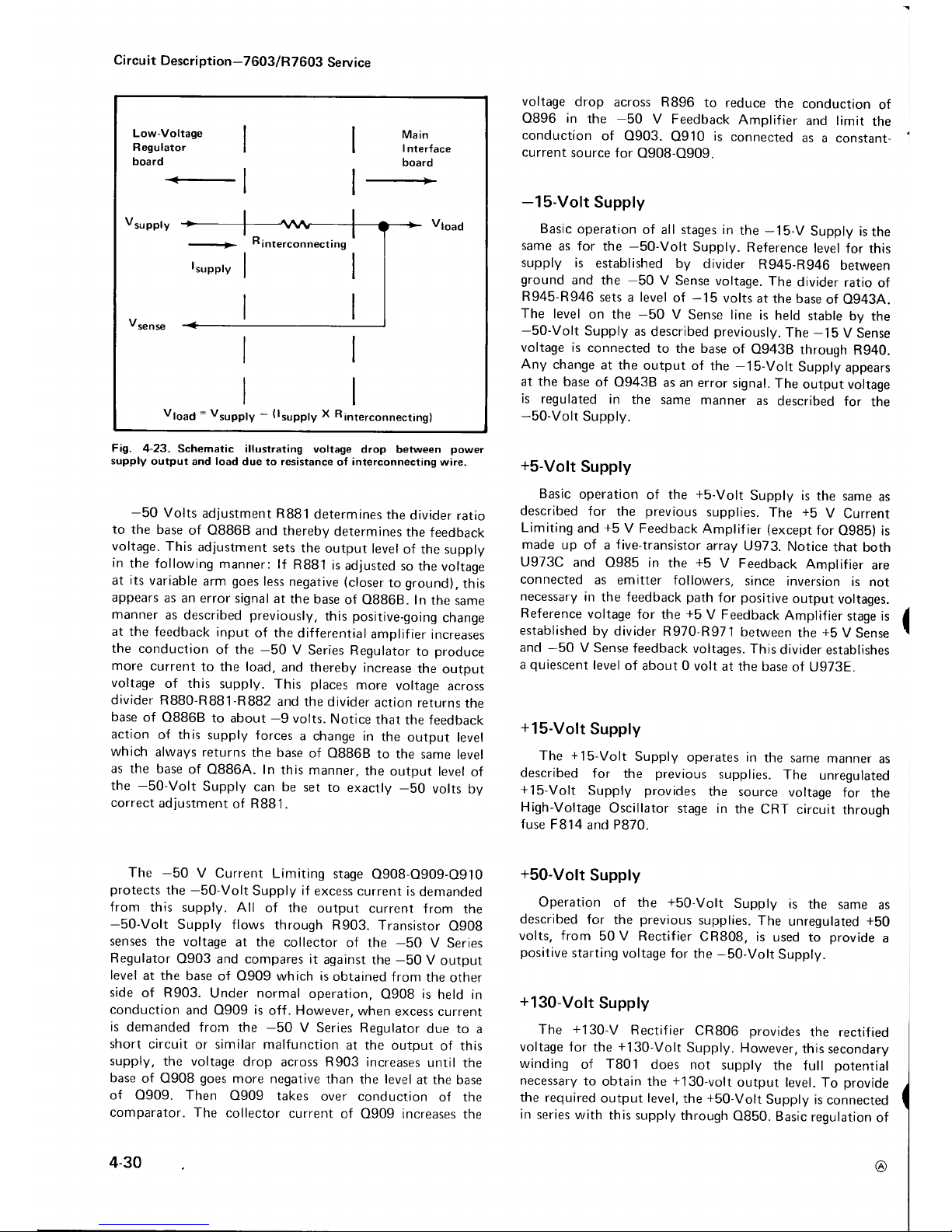
Low-Voltage
Regulator
board
+-_
Main
I
nterface
board
+
Vsupply
Vs"nre
Vload = Vsupply
-
(lsrpply
X Rinterconnecting)
Circu
it Descri
ption-7603/R
7603
Service
Fig.
4-23.
Schematic illustrating
voltage drop
between
power
supply
output
and
load
due 1o resistance
of
interconnecting
wire.
-50
Volts
adjustment R881
determines
the
divider
ratio
to
the base
of 08868
and therebv
determines
the
feedback
voltage.
This
ad
justment
sets
the
output
level
of the supply
in
the following
manner:
lf
R881
is
adjusted
so the
voltage
at
its
variable
arm
goes
less
negative
(closer
to
ground),
this
appears
as an error signal
at
the base
of 08868.
In
the same
manner
as described
previously,
this
positive-going
change
at the
feedback
input
of the
differential
amplifier
increases
the conduction
of
the
-50
V Series
Regulator
to
produce
more
current
to the load,
and
thereby increase
the
output
voltage
of this
supply. This places
more
voltage
across
divider R880-R881-R882
and the divider
action
returns
the
base
of
08868
to about
-9
volts.
Notice
that
the feedback
action
of this
supply forces
a change
in
the
output
level
which
always returns
the base
of O8868
to the
same
level
as the
base
of 08864.
In
this manner,
the
output
level
of
the
-S0-Volt
Supply
can
be set
to
exactlv
-50
volts
bv
correct
adiustment
of
R881.
The
-50
V Current
Limiting
stage
O908-O909-O910
protects
the
-50-Volt
Supply if
excess
current is
demanded
from
this supply. All
of the
output
current
from the
-SO-Volt
Supply
flows through
R903. Transistor
Og08
senses
the voltage
at
the
collector
of the
-50
V
Series
Regulator
0903 and compares it
against the
-50
V
output
level
at the base
of 0909 which is
obtained from
the
other
side
of R903.
Under normal
operation,
0908
is
held in
conduction
and 0909
is
off
. However,
when
excess current
is
demanded
from the
-50
V Series
Regulator
due to
a
short
circuit
or similar malfunction
at the
output
of this
supply,
the voltage
drop
across Rg03 increases
until
the
base
of Q908
goes
more negative
than
the
level
at the base
of 0909. Then
0909 takes
over conduction
of the
comparator. The
collector
current
of 0909 increases
the
4-30
voltage
drop
across R896
to reduce
the conduction
of
0896 in
the
-50
V Feedback
Amplifier
and limit
the
conduction
of 0903.
0910
is
connected
as
a constant-
current
source for
0908-0909.
-15-Volt
Supply
Basic
operation
of all stages
in
the
-15"V
Supply
is
the
same
as for
the
-50-Volt
Supply.
Reference
level
for
this
supply
is
established
by
divider
R945-R946
between
ground
and the
-50
V Sense
voltage.
The
divider
ratio
of
R945
R946
sets a level
of
-15
volts
at the base
of O943A.
The
level
on the
-50
V
Sense line
is
held
stable
by
the
-50-Volt
Supply
as
described
previously.
The
-l5
V Sense
voltage is
connected
to the base
of O943B
through
R940.
Any
change
at the
output of
the
-15-Volt
Supply
appears
at the base
of O9438
as an error
signal.
The
output voltage
is
regulated
in
the same
manner
as
described
for
the
-50-Volt
Supply.
+S-Volt
Supply
Basic
operation
of the
+s-Volt
Supply is
the
same
as
described
for
the
previous
supplies.
The
+5
V
Current
Limiting
and
+5
V Feedback
Amplif
ier
(except
for
O98b) is
made
up of a f
ive-transistor
array
U973.
Notice
that
both
U973C
and
0985 in
the
+5
V Feedback
Amolifier
are
connected
as emitter
followers,
since inversion
is
not
necessary
in
the feedback
path
for
positive
output
voltages.
Reference
voltage
for the
+5
V Feedback
Amplif
ier
stage is
established
by divider
R970-R97
1
between
the
+5
V
Sense
and
-50
V
Sense feedback
voltages.
This
divider
establishes
a
quiescent
level
of
about 0 volt
at the
base
of U973E.
+15-Volt
Supply
The
+15-Volt
Supply
operates in
the
same
manner
as
described
for
the
previous
supplies.
The
unregulated
+15-Volt
Supply
provides
the source
voltage
for
the
High-Voltage
Oscillator
stage in
the
CRT
circuit
through
fuse
F814
and P870.
+50-Volt
Supply
Operation
of the
+50-Volt
Supply
is
the
same
as
described
for the
previous
supplies.
The
unregulated
+50
volts,
from
50 V Rectifier
CR808,
is
used to
provide
a
positive
starting
voltage for
the
-50-Volt
Supply.
+130-Volt
Supply
The
+130-V
Rectifier
CR806 provides
the rectified
voltage
for the
+130-Volt
Supply.
However,
this
secondary
winding
of
T801
does not
supply
the
full
potential
necessary
to
obtain the
+'l
JQ-y611
output
level. To
provide
the
required
output level,
the
+50-Volt
Supply
is
connected
in
series
with
this supply
through
0850.
Basic
regulation
of
@
Page 77

the
output
voltage
is
provided
by
+130
V Feedback
Amplifier 0852, and
+130
V Series
Regulator 0850.
The
output
voltage
of this supply
is
connected across
divider
R855-R856.
This
divider
provides
a
quiescent
level
of about
+50
volts at
the base of 0852.
The
reference
level
for this
supply
is
provided
by the
+SO-Volt
Supply
connected
to the emitter
of
0852.
lf the
output
of this
supply
changes,
this change
is
sensed
by 0852 and an
amplified
error signal
is connected to
the base of 0850.
This error
signal
changes the
conduction of the
+130
V
Series
Regulator
0850
to correct the output
error.
Fuse
F855
protects
this
supply
if
the output
is
shorted.
However,
since the
response time of
F855
is slow to a
shorted
condition,
VR851
provldes
additional
current to
the
base
of 0850
to
protect
it
from
damage due
to
overvoltage.
Diode
CR852
limits the reverse bias
on
0852
to about
0.6 volt
when F855 is blown.
Graticule
Light Supply
Power for
the
graticule
lights
is
supplied
by the Graticule
Light
Supply.
Rectif
ied voltage for this supply
is
provided
by 5
V Rectifier
CR820 CR82
1. 0835 operates as a
series
regulator transistor.
Emitter follower 0829
determines
the
conduction
of this
series
regulator as controlied
by front
panel
GRATICULE
ILLUM Control
R1095.
Current-
limiting
to
protect
this supply
is
provided
by
0827.
Under
normal operation,
divider
R830 R831-R833
sets the
base of
0827
below
its
conduction
level.
However,
if
excess
current
is
demanded
from
this supply,
the voltage drop across
R837-R838
increases until 0827
comes
into conduction.
The collector of
A827 then
limits the conduction
of this
supply to
limit its
output
current.
Divider
R822-R823
provides
a sample of
the line voltage
in the secondary
of
T801 to the
plug-in
unit.
This
provides
a
line-frequency
reference
to the
plug-in
units for
internal
triggering
at
line frequency or
for other applications.
DC Fan
(R7603
only)
The DC
fan
(Option
5) uses a
brushless, Hall-effect
motor.
The Hall-effect devices,
located
inside
the
motor
housing,
control the
base current
to motor-driving
tran-
sistors O1034
O1035-O1037
O1038
depending
upon
the
magnitude and
polarity
of the
magnetic f
ield
around
them.
A
permanent
magnet,
located in the rotor,
changes the
magnetic
field as the rotor
turns,
causing the Hall-effect
devices
to turn on the appropriate
transistors to drive
the
motor windings.
Transistor
O1041
provides
a constant
current source
for
the
Hall-effect
devices,
responding to voltage
changes
at the
emitters of
the driving
transistors,
thus controlling
the
@t
Circu it Descri
ption-7603/R7603
Service
motor
current. Transistor
O1030,
along with R
1203,
provides
a
biasing arrangement
to make the
Hall-effect
devices compatible
with the silicon
driving
transistors.
SIGNAL
OUT BOARD
VERT
SIG OUT
The vertical
signal
is selected
by
the
TRIG
SOURCE
switch.
The vertical
signal selected
is
applied to
the bases of
a
differential
amplifier
0606 and
0618. A single-ended
signal
is taken off
the collector
of 0618 and
connected
to
an
output
buffer 0620.
CR621 and
CR622
provide
protection
against
a high
voltage
inadvertently applied
to
the output
connector.
+
GATE
OUT
The
gate
signal is connected
to a comparator
circuit
0662 and
0666 through
resistor R660. From the com-
parator
the
gate
signal
is connected
to the emitter of an
output buffer 0672.
Gate Selector
switch connects one
of
the
gate
signals
to R660,
the input of the Gate Amplifier.
Possible
gate
signals are
MAIN
gate
and,
with a dual-sweep
time-base
unit,
a DELAY
or an AUXILIARY
gate
signal can
be selected. CR674
and CR676
provide protection
against
a
high voltage
inadvertently
applied to the output connector.
+
SAWTOOTH
OUT
The
sawtooth signal
is connected
to the
Sawtooth
Amplif
ier through R36. 0631,
0634, and 0640 comprise
a
negative
feedback
amplif
ier with a
gain
of two,
determined
bv the
ratio of
feedback
resistor R645 to the combined
input resistance of
R630 and R63. CR635
and CR676
provide protection
against
a high
voltage
inadvertently
applied
to the output connector.
READOUT SYSTEM
The Readout System
in the 7603
provides
alphanumeric
display of
information encoded
by the
plug
in
units.
This
display
is
presented
on
the CRT and
is written by the CRT
beam on a
time-shared
basis. Schematics
for
the total
Readout
System are
shown on diagrams at
the rear of this
manual.
The
deflnitions of
several
terms must be clearly under-
stood to follow
this description of
the Readout System.
These
are:
Character-A
character
is a single number,
letter,
or symbol
which
is
displayed
on the
CRT,
either
alone or
in
combination
with other
characters.
4-31
Page 78
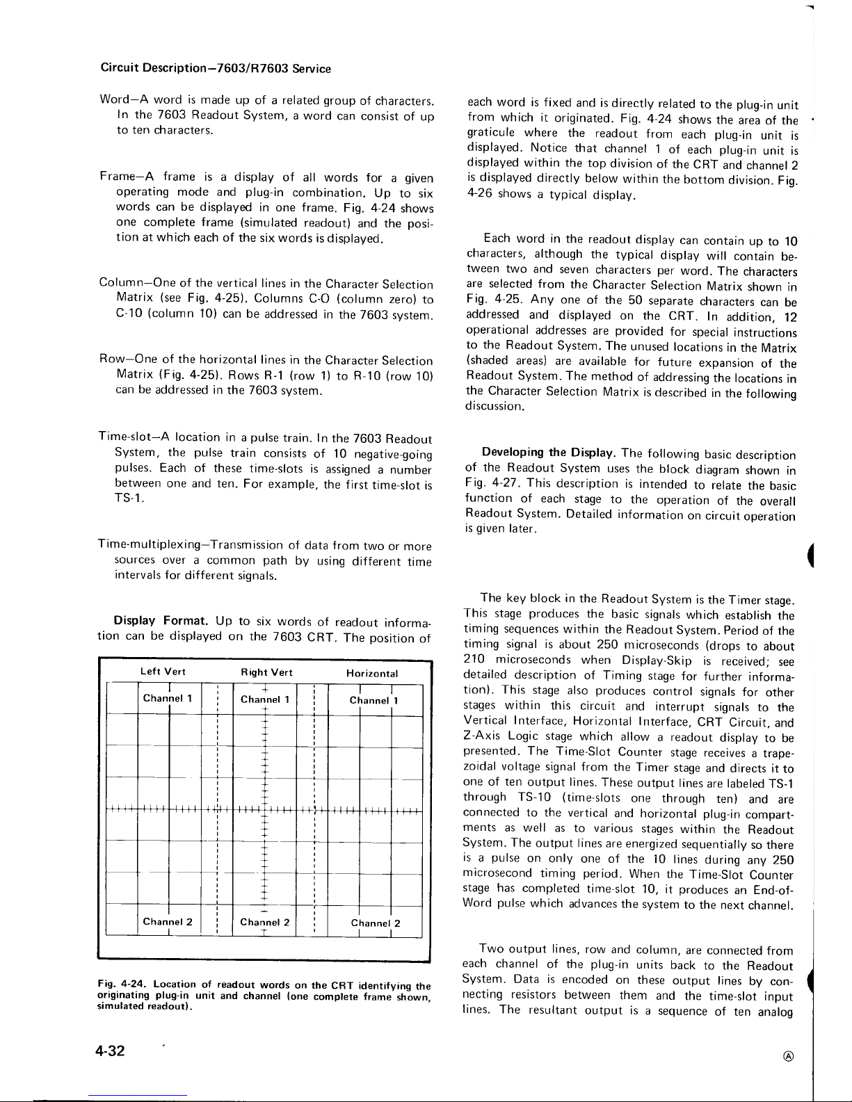
Circuit
Description-7603/R7603
Service
Word-A
word is made
up
of a
related group
of characters.
ln
the 7603
Readout
System,
a word
can consist
of up
to ten characters.
Frame-A
frame
is a display
of all words
for
a
given
operating
mode and
plug-in
combination.
Up
to six
words
can be displayed
in one frame.
Fig. 4-24
shows
one
complete frame
(simulated
readout)
and the
posi-
tion
at which
each of
the six words
is displayed.
Column-One
of the vertical
lines in
the
Character
Selection
Matrix
(see
Fig. 4-25).
Columns
C-O
(column
zero)
to
C-10
(column
10)
can be
addressed
in
the 7603
svstem.
Row-One
of
the
horizontal
lines in
the
Character
Selection
Matrix
(Fig.4-25).
Rows
R-1
(row
1) to R-10
(row
10)
can be
addressed in
the 7603
svstem.
Time-slot-A
location
in
a
pulse
train. In
the 7603
Readout
System,
the
pulse
train
consists
of 10 negative-going
pulses.
Each
of
these time-slots
is
assigned
a
number
between
one and ten.
For
example,
the first
time-slot
is
TS.1.
Time-multiplexing-Transmission
of
data f
rom
rwo
or more
sources
over
a common
path
by
using
different
time
intervals
for
different
siqnals.
Display
Format.
Up to
six words
of readout
informa-
tion can be displayed
on the 7603
CRT.
The
position
of
each
word
is fixed
and is
directly
related
to
the
plug-in
unit
from
which it
originated.
Fig.
424
shows
the
area
of
the
graticule
where
the readout
from
each
plug-in
unit
is
displayed.
Notice
that
channel
1
of
each
plug-in
unit is
displayed
within
the
top
division
of the
CRT
and
channel
2
is
displayed
directly
below
within
the bottom
division.
Fio.
4-26
shows
a
typical
displaV.
Each
word in
the readout
display
can
contain
up
to
10
characters,
although
the
typical
display
will
contain
be_
tween
two
and
seven
characters
per
word. The
characters
are selected
from
the Character
Selection
Matrix
shown
in
Fig.4-25.
Any
one
of the
50
separate
characters
can
be
addressed
and
displayed
on the
CRT.
In
addition,
12
operational
addresses
are
provided
for
special
instructions
to the
Readout
System. The
unused
locations
in
the
Matrix
(shaded
areas)
are available
for
future
expansion
of the
Readout
System.
The
method
of addressing
the locations
in
the
Character
Selection
Matrix
is
described
in
the
following
d
iscussion.
Developing
the
Display.
The
following
basic
description
of the Readout
System
uses
the block
diagram
shown
in
Fig. 4-27
.
This
description
is
intended
to relate
the
basic
function
of each
stage
to the
operation
of
the
overall
Readout
System.
Detailed information
on
circuit
operation
is
given
later.
The
key block in
the Readout
System
is
the Timer
stage.
This
stage
produces
the
basic signals
which
establish
the
timing
sequences
within
the Readout
Svstem.
Period
of the
timing
signal is
about 250
microseconds
(drops
to about
210
microseconds
when
Display-Skip
is
received;
see
detailed
description
of Timing
stage
for further
informa-
tion).
This
stage
also
produces
control
signals
for
other
stages
within
this
circuit
and interrupt
signals
to
the
Vertical
Interface,
Horizontal
lrrterface,
CRT
Circuit.
and
Z-Axis Logic
stage
which
allow
a readout
display
to be
presented.
The
Time-Slot
Counter
stage receives
a rrape-
zoidal
voltage
signal
from
the Timer
stage
and
directs it
to
one
of ten
output lines.
These
output lines
are labeled
TS-1
through
TS-10
(time-slots
one through
ten)
and
are
connected
to the vertical
and horizontal plug-in
compart-
ments
as well
as to various
stages
within
the Readout
System.
The
output lines
are
energized
sequentially
so there
is
a
pulse
on
only
one of the
10 lines
during
any
2SO
microsecond
timing
period.
When
the
Time-Slot
Counter
stage
has
completed
time-slot
10, it
produces
an End-of-
Word
pulse
which
advances
the system
to the
next
channel.
Two
output lines,
row
and column,
are connected
from
each
channel
of the
plug-in
units back
to the
Readout
System.
Data is
encoded
on these
output
lines
oy con-
necting
resistors
between
them
and
the
time-slot
input
lines.
The
resultant
output is
a sequence
of ten
analog
(
Fig,
4-24,
Location
of
readout
words
on the
CRT identifying
the
originating
plug-in
unit
and
channel
(one
complete frame
shown,
simulated readout).
4-32
Left
Vert
R ight
Vert
Horizontal
Channel
1
I
i
Channel
1
tl
Channel
1
ll
I
Channel
2
I
Channel
2
t
c
hannel
2
@
Page 79

r
s
o
N
D
N
o
o
Circu
it Description-7603/R7603
Service
F
x
U
F
z
Yz
FA
tn:
>F
(,/)
o-
- .r
OU'
U
ao
llJ
r
4U
|rF
o9
Zfr
Y
@-
zo
{r
2=
uo
46ccJ
l
iE
io
ccH
o
Lt!
,,.
uJ
-to
<il
JF
;
gis
@oI
zoo
9
FJZ
H =;
:v
^F
il S=
th*;
-4
U
zAn
/{
g!
o
tr.
a
t!
q
lrt
OO
F-
ir
2=
o
\
()
()
ts
\
(o
>
E a
\
o.
z
{FYx
i4\;
oYoz
3-9
rc)
v
\
a-
z
<tsYo
Eiio
(JYOz
LT'
\t
+
x
.F
z
S5ir
=A<o
exoz
o:
I
s
c5
'*r
| 3-P
:il
<fr
ilrl
?,3
\
\l
G,
z
*5i:
==<o
oYoz
H-9
F?
N
F{
oXr
F=
|
L* |
-trJ
I
;r
t
c
o,
z
<Efo
Eal;
OY(Jz
oi
N
N
^o
oEg
<-ft
.
'n:
E
<vN
V)
o
6;'i
oa.z_:
o=
o
=tr |
-m I
:=
|
ozl
z:ii
uJJr
CE<L
l5E
O<
N
m
I
$
\
__l}c(
=H
Y>
-f
z
(r
ql
cc
Y
to F q
4-33
Fig.4-25.
Character
Selection Matrix
for
7603
Readout
Svstem.
REV
C MAR 1981
Page 80

lv 90a ,s
I
I \
/
\
I
\ I
\
I
\ /
\
-l
Circuit Description-7603/R7603 Service
Fig,
4-26,
Typical readout display
where
only channel
1 of the
Right
Vertical and Horizontal
units is displayed,
current levels
which range from zero
to
one milliampere
(100
microamperes/step)
on the row
and column
output
lines. This
row and column
correspond
to the row
and
column
of
the
Character Selection Matrix in
Fig. 4-25. The
standard format in
which
information
is
encoded
onto
the
output
lines is
given
in f
able
4-2
(special
purpose plug-in
units may have
their own format
for readout; these
special
formats
will
be
def
ined
in the manuals
for
these units).
The
encoded column
and row
data from the
plug-in
units is
selected by the Column
Data Switch
and Row Data
Switch stages
respectively. These
stages take
the analog
currents
from
the six data lines
(two
channels from
each
of the three
plug-in
compartments)
and
produce
a single
time-multiplexed
analog voltage
output which contains
all
of the column
or
row information
from the
plug-ins.
The
Column
Data Switch
and
Row
Data Switch
are seouenced
by
the binary
Channel
Address
No.
l code
from the
Channel
Counter.
The
time multiplexed
output
of the Column
Data
Switch is monitored
by
the Display-Skip
Generator
to
determine if it represents
valid information
which should
be
displayed. Whenever information
is
not
encoded in
a
time-slot,
the Display-Skip
Generator
produces
an output
level
to
prevent
the
Timer
stage f rom
producing
the control
signals
which normally interrupt
the CRT
display
and
present
a character.
The
analog
outputs of the Column Data
Switch
and Row
Data
Switch
are
connected
to the Column
Decoder
and
Row Decoder
stages respectively. These
stages
sense the
magnitude
of the analog voltage input
and
produce
arr
4-34
output current
on one of ten lines.
The
outputs
of the
Column
Decoder stage
are
identified
as
C-1
to C-10
(column
1to
10) which correspond
to the
column
information
encoded by
the
plug-in
unit. Likewise,
the
outputs
of the Row Decoder
stage
are identified
as
R-1
to
R-10
(row
1to 10) which
correspond
to the row
information
encoded by the
plug-in
unit. The
primary
function
of
the row
and column
outputs is
to select
a
character
from
the Character
Selection Matrix
to
be
produced
by
the Character
Generator stage.
However.
these
outputs
are also used
at other
points
within the
system to
indicate
when certain information
has been
encoded.
One
such
stage
is
the Zeros Logic
and Memory.
During
time-slot
1
(TS-1),
this
stage checks if
zero-adding
or
prefix-shifting
information
has been
encoded by
the
plug-in
unit and
stores it in
memory
until time-slots
5,6,
or 8.
After
storing
this information,
it
triggers the
Display-Skip
Generator
stage so
there
is
no display
during
this time
slot
(as
defined
by
Standard Readout
Format;
see Table
4-2).
When
time-slots
5, 6,
and 8 occur, the
memory is
addressed
and
any information
stored
there during
time-slot
1 is trans-
ferred
out and connected
to the input
of the Column
Decoder
stage to mod ify
the
analog
data
during the
applicable time-slot.
TABLE 4-2
Standard
Readout
Format
Time-Slot
Number
Description
t5-l
D
ete r m
ines
decimal magnitude
(number
of zeros
displayed or
pre-
f ix
change information)
or
the
IDENTIFY
f unction
(no
display
during th is time-slot).
TS2 Ind icates
normal
or
inverted input
(no
display for
normal).
TS3 I ndicates
calibrated
or uncalibrated
condition
of
plug-in
variable con-
trol
(no
display for
calibrated con-
d
ition
)
.
TS.4
1-2-5 scaling.
TS5
TS6
TS.7
Not encoded
by
plug-in
unit.
Left
blank to
allow addition
of
zeros bv
Readout
Svstem.
Defines the
prefix
which
the units
of
measurement.
Def ine
the units
of
measurement
of
the
plug-in
unit.
May
be standard
units
of
measurement
(V,
A,
S,
etc.,)
or
special
units selected from
the Character
Selection Matrix.
TS8
TS.9
TS
10
@
Page 81

Another
operation
of the Zeros
Logic
and Memory
stage
is
to
produce
the IDENTIFY
function.
When
time-slot
j
is
encoded
for IDENTIFY
(column
i0,
row
3), this
stage
produces
an
output level
which connects
the Column
Data
Switch
and Row
Data
Switch
to
a coding network
within
the Readout
System.
Then,
during
time-slots
2
through
9,
an analog
current
output is
produced
from
the
Column
Data Switch
and Row Data
Switch
which
addresses
the
correct
points
in
the Character
Selection
Matrix
to display
the word
"IDENTIFY"
on
the CRT. The
Zeros
Logic
and
Memory
stage is
reset
after
each
word by
the Word
Trigger
pu
lse.
The
Character
Generator
stage
produces
the
characters
which
are
displayed
on the
CRT. Any
of the
50
characters
shown
on the Character
Selection
Matrix
of
Fig.
4-24
can
be
addressed
by
proper
selection
of
the column
and row
current.
Only
one character
is
addressable
In
anv
one
time-slot;
a
space
can be
added into
the
displayed
word by
the Decimal
Point
Logic
and Character
Position
Counter
stage
when
encoded by
the
plug-in.
The
latter
stage
counts
how many
characters
have been
generated
and
produces
an
output current
to step
the display
one character
position
to
the
right
for
each character.
In
addition,
the
cnaracter
position
is
advanced
once
during
each
of time-slots
1, 2,
and
3
whether
a character
is
generated
during
these
trme-slots
or not.
This
action
fixes
the
starting
point
of
the
standard-format
display
such
that
the
first
digit
of the
scaling
factor
always
starts
at the
same
point
within
each
word
regardless
of the information
encoded in
time-slot
2
(normal/invert)
or
time-slot
3
(calluncal)
which
precedes
this
digit. Also,
by
encoding
row
10
and
column
0 during
any time-slot,
a blank
space
can
be
added
to the
disolav.
Decimal
points
can be
added
to
the display
at
any time by
addressing
row 7
and
columns
3
through
7
(see
Character
Selection
Matrix
for
location
of these
decimal
points).
The
Decimal Point
Logic
and Character
position
Counrer
stage
is
reset
after
each word by
the
Word Trigger pulse.
The
Format
Generator
stage
provides
the
output signals
to the
vertical
and horizontal
deflection
systems
of the
instrument
to
produce
the
character
dispray.
The
binarv
Channel Address
No. 2
code
from
the
Channel
Counter
stage is
connected
to this
stage
so that
the
display
from
each channel
is
positioned
to the
area
of the
CRT which
is
associated
with
the
plug-in
and
channel
originating
the
word
(see
Fig.
4241
. The
positioning
current
or
decimal
point
location
current
generated
by
the
Decimal
point
Logic
and
Character
Position
Counter
stage is
added
to the
horizontal
(X)
signal
at the input
to the Format
Generator
stage
to
provide
horizontal
positioning
of the
characters
within
each
word. The
X
and Y-output
signals
are
connected
to the Horizontal
Amplif
ier
and Vertical
Ampli-
fier
through
the Horizontal
Output
and Vertical
Output
stages
respectively.
The
Word
Trigger
stage
produces
a trigger
from
the
End-of-Word pulse
generated
by
the Time-Slot
Counter
REV
B, IVIAY 1978
Circuit
Description-7603/R7603
Service
stage
after
the tenth
time-slot.
This
Word
Trigger
pulse
advances
the
Channel
Counter
to display
the information
from
the next
channel
or
plug-in.
lt
also
provides
a
reset
pulse
to
the Zeros
Logic
and Memory
stage
and the Decimal
Point
Logic
and Character
Position
Counter
stage. The
Word
Trigger
stage can
also be
advanced
to
jump
a
complete
word
or
a
portion
of a
word
when
a Jump
command
is
received
from
the Row
Decoder
staqe.
The
Single-Shot
Lockout
stage
allows
the
display
se-
quence
of the
Readout
System
to
be
changed.
Normally,
the Readout
System
operates in
a f ree-running
mode
so
the
waveform
display is
interrupted
randomly
to display
characters.
However,
under
certain
conditions
(such
as
single-shot photography),
it
is
desirable
that
the Readout
System
operate in
a triggered
mode
where
the readout
portion
of the
display
is normally
blanked
out but
can be
presented
on command.
The
Readout
Mode
switch deter-
mines
the
operating
mode
of the
readout
svstem.
Circuit
Analysis
of
Readout
System
The
following
analysis
of the
Readout
Svstem
describes
the
operation
of each
stage in
detail.
Complete
schematics
of
the
Readout
System
are shown
on
diaqram
10
at the
read
of this manual.
Timer
Timer
U2126
establishes
the
timing
sequence
for
all
circuits
within
the
Readout
System.
This
stage
proouces
seven
time-related
output
waveforms
(see
Fig.
4-2g).
The
triangle
waveform
produced
at
pin
6
forms
the basis for
the
remaining
signals.
The
basic
period
of this
triangle
wave_
form
is
about
250 mrcroseconos
as
controlled
bv RC
network
C2135-R2135.
The
triangle
waveform
is
clipped
and
amplified
by
U2126
to form
the
trapezoidal
output
signal
at
pin
10.
The
amplitude
of
this output
signal is
exactly
'l
5 volts
as
determined
by
U2126
(exact
amplitude
necessary
to
accurately
encode
data
in
plug_in
units;
see
Encoding
the Data).
The
Trigger
output
at
pin 5 provides
the
switching
signal
for
the
Time-Slot
Counter
and Word
Trigger
stages.
The
signals
at
pins
12,13,14,
and 16
are
produced
only
when
the
triangle waveform
is
on
its
negative
slope
and the
trapezoidal
waveform
has
reached
the lower
level. The
timing
sequence
of these
waveforms
is
very
important
to
the correct
operation
of the
Readout
System
(see
expanded
waveforms
in Fig. 4 29).
The
Z-Axis
Logic
OFF Command
at
pin
i4 is
produced
first. This
negative-going
signal
provides
a
blanking
pulse
to the
Z-Axis
Logic
stage
(see
diagram 2)
to blank
the
CRT before
the
display
is
switched
to
the Readout
System.
lt
also
produces
the
Strobe
pulse
through
R2131
,
O2138,
and
CR2142
to signal
other stages
within the
Readout
System
to begin
the
sequence
necessarv
4-35
Page 82

Control
pulses
to
Vert. In-
ter., Horiz.
lnter.,
CRT Ckt
and Z-Axis
Logic stage.
{Skip
if
data encoded
in TS-11
(Skip
if no
column
data
encoded
in
q---------
this
time-slotl
Time-multiplexed
analog voltages
(Display
skipl
Ci rcu it Description-7603/R7603
Service
plug-in
com.
partments
Time-slot
pulses
to vertical
and
horizontal
plug-
in
compart-
ments.
Data
encodod by
resistors
in
plug-in
units
I
T
tl
/ \
*,u-n "n",on
I
data
in from
I
Plug-in
com-
I
partments
I
I
\
\
\
\
\
\
Ro*
"n"tog
data in from
/
(
I
I
\
(IDENTIFYI
@
Timer
u2126
o2138
I
(TS-2
to
TS-91
Fig. 427. Detailed
block diagram of Readout
System.
4-36
Page 83

Circuit
Description-7603/R7603
Service
NOTE:
Indicates
number
of lines.
n
r\
Where
no number
appears;
there
is
one
line.
(
Readyl
{Channel
Address
No.2l
(c-1
to
c-10)
(R-1,
R-2, R-4
R-5, R-61
Y-Signal to
Vertical
Amplif
ier
)
X-Signal to
Horizontal
Amplifier
Decimal
point
Logic
and
Character
Position
Counter
u2260
(R-7,
R-101
2
{TS-1,
TS-5,
T5-6. TS.8)
(c-3
to c-71
(Zero-adding
and
prefix-
shifiing
data)
(Character
positionl
(Character
scan)
Format
Generator
u2244
Ai
Fig. 427. Detailed
block diagram
of Readout
System
(cont).
4-37
Page 84

Circuit
Description-7603/R7603
Service
Fig.4-28.
Output waveforms
of Timer
stage.
4-38
Fig.4-29.
Detail
of outputs
ar
pins
12, 13,
14,
and 16
ot 1J2126.
to
produce
a character.
The
collector
of 02138
is
also
connected
to
Character
Generator
No. 2,
U2272
through
C2140,
CR2140. This
activated
U2272
during
the
quiescent
period
of the
Strobe
pulse
(collector
of 02138
negative)
and diverts
the
output
current
of Row
Decoder
U2185 to
row
2.
The
purpose
of
this
conf iguration
is
to
prevent
tne
Zeros
Logic
and Memory
stage
U2232
from
storing
incorrect
data
during
the
quiescent
period
of the
Strobe
pulse.
When
the
Strobe
pulse
goes positive,
CR2140
is
reverse
biased
to
disconnect
02138
|rom
1J2272
and
allow
the Row
Decoder
stage
to
operate in
the normal
manner.
The
next
signal
to be
produced
is
the Vertical/
Horizontal
Channel
Switch
OFF Command
at
pin
13. This
positive-going
signal
disconnects
the
plug-in
signals in
the
vertical
and horizontal
deflection
systems
so
the
plug-in
units
do not
control
the
position
of the CRT
beam
during
the
readout
display. The
Ready
signal
derived
from
this
output is
connected
to
the Decimal
Point
Logic
and
Character
Position
Counter
stage
and
the Format
Generator
stage
(see
diagram
10). The
Readout
Intensity
output
at
pin
12
is
produced
next. This
current
is
connected
to the
CRT
Circuit
to
unblank
the
CRT to
the intensity
level
deter-
mined
by
READOUT
intensity
control
R2j24.
The
Char-
acter
Scan ramp
at
pin
16
started
to
go
negative
as
this
@
Pin 1O
Trigger
Pin 5
Character
Scan
Pin 16
Z-Axis
Logic
OFF
Command
Pin
14
Vertical
and
Horizontal
Channel
Switch
OFF
Command
Pin
13
Readout
InterBity
Pin 12
NOTE:
Test
oscilloscope
ex t€r nally
triggered
lromTp2251
.
tt
20a
.:s
I
I
I
5Y
20a
s
tf
201 s
tl
il It II
Character
Scan
Pin
16
Z-Axis
Logic
F
Command
Pin
14
Vertical
and
Horizontal
Channel
Switch
OFF
Command
Pin 13
Readout
Intomity
Pin
12
NOTE: Test occilloscope extornally
triggered
from
Tp2251.
tr
2ot
'J
2ot
lv
2ot
Page 85

timing sequence
began. However,
charactergeneration
does
not
start until
the readout intensity
level has
been
established. The triangular
Character
Scan ramp
runs
negatively from
about
-2
volts
to
about
-8.5
volts
and
then returns
back to the
original level. This
waveform
provides
the scanning
signal for
the Character
Generator
stages
(see
diagram
10). The Full
Character
Scan adjust-
ment R2128
sets the
DC level
of
the
Character
Scan ramo
to
provide
complete characters
on the display.
The
Timer
stage operates in
one
of two modes
as
controlled by
the Display-Skip
level
at
pin
4. The
basic
mode
just
described
is
a
condition
which
does nor
occur
unless
all ten
characters of each word
(60
characters
total)
are displayed on
the CRT. Under
typical
conditions
only a
few
characters
are displayed
in
each word. The
Display-Skip
level
at
pin
4
determines
the
period
of
the Timer
output
signal.
When a character
is to
be
generated, pin
4 is LO
and
the circuit
operates
as
iust
described. However,
when
a
character is
not to be
displayed,
a Hl level
is
applied to
pin
4
of U2126
through CR2125
from
the Disptay-Skip
Generator
stage. This
signal causes
the Timer
to shorten
its
period
of operation
to about 210
m icroseconds.
The
waveforms
shown
in
Fig. 4 30
show
the
operation
of the
Timer
stage when the
Display-Skip
condition
occurs for
all
positions
in
a word. Notice
that
there is no
output
at
pin
12, 13,
14,
and
i6
under this
condition. This
means
that
the
CRT display is
not interrupted
to
display
characters.
Also
notice
that the
triangle waveform
at
pin
6 does not
go
as far negative
and that the negative
portion
of the
trapezoidal
waveform
at
pin
10
is
shorter.
Complete
details
on operation
of
the
Display-Skip
Generator
are
given
later.
The
Single-Shot
Lockout
level
at
pin
2
determines
the
operating mode
of U2126. lf
this level is
LO,
the Timer
operates
as
lust
described.
However,
if
the
Single-Shot
Lockout
stage sets
a Hl level
at this
pin,
the Timer
stage is
locked
out
and can not
produce
any
output signals
(see
Single-Shot
Lockout
description
for further
information).
The
READOUT
intensity
control
R2'124
sets the inten-
sity
of the readout
display independently
of
the
INTEN
SITY control.
The R
EADOUT intensity
control
also
provides
a
means
of
turning
the Readout
System
off when
a
readout
display is
not desired.
When R2124
is
turned fully
counterclockwise,
switch
Si02
opens. The
current
to
pin
11 of
U2126
is interrupted
and
at the same
time
a
positive
voltage is
applied to
pin
4
through
R2122
and CR2124.
This
positive
',,oltage
swiiches
the stage
to the
same
conditions
as \ryere
present
under the
Display-Skip
con-
dition.
Therefore,
tlre CRT
display is no1
interrupted
to
present
characters.
Hov;ever,
tinte-slot
pulse
continue
to be
generated.
Circuit
Description-7603/R7603
Service
Pin
6
Pin 1O
Trigger
Pin
5
OV
Character
Scan
Pin 16
Vertical
and
Horizontal
Channel
Switch
OFF
Command
Pin
13
I
ntensity
Pin
12
-+6
V
NOTE:
Test
9J
20a s
Z-Axis
Logic
oscif loscope
externally
triggered
lrom Tp2251
Fig.4-30.
Timer
stage operation when Display-Skip
condition
occu
rs.
4-39
Page 86

Circuit
Description-7603i
R7603
Service
Time-Slot
Counter
Time-Slot
Counter
U2126 is
a sequential
switch
which
directs
the trapezoidal
waveform
input
at
pin
8 to one
of its
10
output lines.
These
time-slot
pulses
are
used
to
interrogate
the
plug-in
units
to obtain
data
for the
Readout
System.
The
Trigger
pulse
at
pin
15
switches
the Tinre-Slot
Counter
to the next
output line;
the output
signal
is
sequenced
consecutively
from
time-slot
1 through
time-slot
10. Fig. 4-3
1
shows
the time-relationship
of the
time-slot
pulses.
Notice
that
only one
of the lines
carries
a time-slot
pulse
at any
given
time.
When
time-slot
10 is
completed,
a
negative-going
End-of-Word pulse
is
produced
at
pin
2.
The
End-of-Word
pulse provides
a drive
pulse
for the
Word
Trigger
stage
and
also
provides
an enabling
level
to the
Display-Skip
Generator
during
time-slot
1
only.
Pin
16 is
a reset input
for
the Time-Slot
Counter.
When
this
pin
is held
LO,
the Time-Slot
Counter
resers
to
time-slot
1. The Time-Slot
Counter
can
be
reset in
this
manner
only when
a Jump
signal is
received
bV
U2155C
(see
following
d
iscussion).
Word
Trigger
The
Word Trigger
stage is
made
up
of the 4
two-input
NOR gates
contained
in
U2155.
Ouiescently,
pin
2
of
U2i
55A is
LO
as established
by the
operating
conditions
of
U2i55D
and
U2155C. Therefore,
the LO
End-of-Word
pulse
produced
by
the Time-Slot
Counter
results
in
a Hl
level
at
pin
'l
of U2155A. This
level
is inverted
bv
U2jb5B
to
provide
a negative-going
advance
pulse
to
the Channel
Cou
nter.
An
advance
pulse
is
also
produced
bv
U2155A
when
a
Jump
signal is
received
at
pin
I
ot U2155C. This
condition
can
occur
during any time-slot
(see
Row
Decoder
for
further information
on
origin of the
Jump signal).
U215bD
and U2155C
are connected
as a bistable
flip-fl6p.
ths
positive-going
Jump
signal
at
pin
8
of U2155C
proouces
a
LO
at
pin
10. This
LO is inverted
by
tJ2155D
to
proouce
a
Hl
at
pin
13, which
allows
pin
9
of U2155C
to be
pulled
Hl
through
R2155. The
flip-flop
has
now
been
set
and
it
remains
in
this condition
until
reset,
even
though
the Jump
signal
at
pin
8 returns
to
its
LO level.
The
Hl
outout level
at
pin
13 turns
on
02159 through R2158
to
pullpin
16
of the
Time-Slot
Counter
LO. This
resets
the Time-Slot
Counter
to time-slot
1
and holds it
there
until
U2155C is reset.
At
the same
time, a Hl level is
applied to
pin
4
of the Timer
through
CR2125
and
CR2124.
This
Hl level
causes
rne
Timer
to
operate
in
the
display-skip
mode
so tnat
a
character
is
not
generated.
The
next
Trigger
pulse
is
not
recognized
by
the
Time-Slot
Counter
since U2159 is
locked
in
time-slot
1 by
U2155.
However,
this Trigger
pulse
resets
the Word
Trigger
4-40
Fig.
4'31.
Time relationship
ol
bv U2126.
the
time-slot
(TS)
pulses
produced
@
lrl.l
lPrPt
trl
qlql
?l?l
tl
qlelrl,elelPl
?tPl?t?t
?t?t
tttttl
Time{lot
pulse
1
Pin 3
OV
Time-slot
pulse
2
Pin
13
Timeslot
pulse
3
Pin
12
Time*lot
pulse
4
Pin
11
Timeslot
pulse
5
Pin
10
Time5lot
pulse
6
Pin
9
Time5lot
pulse
7
Pin
7
Time6lot
pulse
8
Pin 6
Time*lot
pulse
9
Pin
5
Timeslot
pulse
10
Pin
4
NOTE: Test
oscilloscope externally triggered from
fP2251.
Sweep rate uncalibrated.
ol
201 s
U
(
Page 87

stage
through
C2155. Pin
'1
3
ot U2155D
goes
LO to
enable
the Time-Slot
Counter
and
Tirner
stages
for the
next
time-slot
pulse.
At
the same time,
the negative-going
edge
produced
af U2155D
switches
output states
which is
connected to
pin
3
of U2155D. This
results in
a
negative-
going
Word
Trigger
output
at
pin
4
of
U21558 to
advance
the Channel
Counter
to the next
word. When
the next
Trigger
pulse
is
received
at
pin
15,
the Time-Slot
Counter
returns
to
the normal sequence
of operation
and
produces
an output
on the time-slot
1 line.
Channel Counter
The
Channel Counter, made
up
o{
integrated
circuit
U2250 is
a binary counter which
produces
the
Channel
Address
code for the Column
and Row Decoder stages
and
the
Format
Generator stage. This
code
instructs
these stages
to sequentially
select and display the
six channels
of
data
from
the
plug-in
units. The input
channel which is
displayed with each combination
of the Channel Address
code
is
given
in the
discussion of the
applicable stages.
Single-Shot
Lockout
O2108,
o'2111
,
and U212O
makes
up
the Single-Shot
Lockout
stage. This
stage allows a single
readout frame
(Six
complete words)
to
be
displayed
on the CRT,
after which
the Readout
Svstem
is
locked
out so further readout
displays
are
not
presented
until
the circuit is reset.
U2120C
and U2120B
are connected to form a bistable
f
lip-f lop.
For
normal
operation,
pin
3
of U212O is
pulled
Hl
through
R2108. This
activates
U212OC to result in
a LO
output
level
at
pin
10. This
level
enables the
Timer
stage
so
it
can
operate in
the free-running manner
as
described
previously.
The
LO at
pin
10
of U212OC is
also applied to
pin
5 of
U21208. Since
pin
6 of U2120A is LO,
U21208 is
disabled
and
its
output
goes
H l.
The
output of this stage remains
LO to
allow U2126 to
operate
in
the free-running mode
until a LO is
received at
pin
8
of
U212OC- When this
occurs, the output level
at
pin
10 of U2120C does not change immediately.
However,
the
Readout
System
is
now
enabled as far
as
the
single shot
lockout function is
concerned. lf
the Channel Counter
has
not
completed word six
(Channel
2
of the
Horizontal
unit),
the Readout System continues
to
operate
in
the normal
manner. However,
when word
six
is
completed,
a
positive,
going
End-of-Frame
pulse
is
produced
at
pin
9 oI
U212OB
as the Channel
Counter shifts to the
code
necessary
to
dlsplay word
one.
This
pulsais
coupled
to
pin
3
of U212OA
and
pin
12
ot U2'120D.
The
momentary Hl
at
pin
3
activates
U21208 and
its
output
goes
LO
to d
isable
U212OC
(pin
3
already
LO). The
output
of U2120C
goes
Hl
to disable the
Timer
so it
operates
in
the display-skip
mode. The Hl
at
pin
10
oI
U212OC
also holds
U212OB
enabled so it maintains control
of the flio-floo.
(a)
Circuit
Description-7603/R7603
Service
The
Single-Shot Lockout
stage remains
in
this
condition
until
a
positive-going
trigger
pulse
is
applied to
pin
8
of
U212OC. This
trigger
pulse produces
a LO
at
pin
10 of
U212OC which
enables U21208
and
disables U212OC.
Now,
the Timer can
operate
in
the
normal
manner for
another complete
frame. When word
six is
completed,
the
Channel Counter
produces
another End-of-Frame
pulse
to
again
lock
out the
Timer
stage.
Encoding
the Data
Data is
conveyed from
the
plug-in
units to
the
Readout
System in
the
form
of an analog code
having up
to
i 1
current levels
(f
rom
zero to
one milliampere in
100
microampere steps). The
characters
which
can be selected
bv
the encoded
data are shown
on the Character
Selection
Matrix
(see
Fig.4 25l'
. Each
character requires
two
currents
to define it; these
currents
are
identified
as the column
current
and the row
current which
correspond
to the
column
and row
of
the matrix. The
column
and row
data
is
encoded by resistive
programming
in
the
plug-in
units. Fig.
4-32
shows a typical
encoding scheme
for
a voltage-sensing
amplifier
plug-in
unit.
Notice
that
the 10
time-slot
(TS)
pulses produced
by
the
Time-Slot
Counter stage
are
connected
to the
plug-in
unit. However,
time-slots
5, 6,l,
and 10
are
not
used by the
plug-in
unit
to encode
data
when
using the Standard
Readout Format
(see
Table
4-2
for
Standard Readout
Format).
The
amplitude
of the
time-slot
pulses
is
exactly
-'l
5 volts
as determined
by the
Timer
stage.
Therefore,
the
resultant
output current
from
the
plug-in
units can be
accurately
controlled by
the
programming
resistors in
the
plug-in
units.
For
example, in Fig. 4-32,
resistors
R
10 through R90
control the
row analog
data which is
connected
back
to the
Readout
Svstem. These
resistors
are
of
fixed
value
and
define
the
format
in which
the information
will be
presented
by
the Readout
System. Fig.
4 33A
shows
an
idealized
output current
waveform
of row
analog
data
which
results from
the 10 time-slot
pulses.
Each
of the
steps
of
current
shown in
these waveforms
corresponds
to
'100
microamperes
of current. The
row
numbers
on
the
left-hand
side
of the waveform
correspond
to
the rows in
the Character
Selection Matrix
shown in
Fig. 4-35.
The
row
analog data is
connected back
to the
Readout
System
via
terminal
B37
of the
plug-in
interface.
The
Column
analog data
is
def ined
by resistors
R110
through
R'l 90.
The
program
resistors
are connected
to the
time-slot lines
by switch closures
to encode
the
desired
data. The
data as encoded by
the
circuit shown in
Fig.4-32
indicates
a 100 microvolt
sensitivity
with
the display
inverted
and calibrated
vertical
deflection
factors. This
results in
the idealized
outDUt
current
waveforms
shown in
Fig.
4 33B
at the column
analog
data
output, terminal A37
of the
plug-in
interface.
Resistor
R111,
connected
between
time-slot
1
and the column
analog data
output,
encodes
two units
of current
during time-slot
1. Referring
to the
4-41
Page 88

Plug-ln
Unit
A33
B32
A32
Row
Analog
Data to
Readout
System
Ti m€- Slot
Pulses
from
Readout
System
831
A31
830
A30
829
A29
Column
Analog
Data
to
Readout
System
437
7
TS'1O
*
*Not
used
in
standard
format.
R1'rO
150
K
TS_2
R2O
150 K
I ^to'
|
R111
75K
.-.........rVv-
'00'
o
R12o
150 K
TS-3
R3O
150
K
lnvert
;
R13o
13 K
TS-4
......n
\--V-V\-
Uncalibrated
R140
75 K
7
TS-S
*
)
ts-6
*
/
TS-7
+
)
rse
R8o
5oK
1
R141
150
K
HAnr-
2
R142
37.4
K
t>-aAz\-
5
R180
150
K
TS-9
R90
37.4
K
o
m
Rr81
7sK
lJ
R190 75
K
Circuit
Description-7603/R7603
Service
Fig.4'32.
Typical encoding
scheme
for
voltage-sensing
amplif
ier
plug-in
unit.
Coding
shown
for
deflection {actor
of 1O0
microvolts.
Character
Selection Matrix,
two units
of column
current
along with
the two
units of row
current
encoded
by
R10
(row
3) indicates
that
two zeros
should
be
added
to the
display. Resistor
R120
adds one
unit
of column
current
during time-slot
2
and along with
the
one unit
of
current
from the
row
output, the Readout
System is
instructed
to
add an
invert
arrow
to the
display. R130 is
not
connected
to the
time-slot 3 line
since
the
vertical
deflection
factors
are calibrated.
Therefore,
there is
no
column
current
output
during this
time-slot
and there is
no
display
on the CRT
(see
Display-Skip
Generator
for further
information).
During
time-slot 4,
two units
of column
current
are
encoded
by R140. There
is
no row
current
encoded
during
this
time-slot
and this results in
the rrumeral
l being
displayed
on the
CRT. Neither
row nor
column
analog data
is
encoded
during time-slots
5,6,
and
7
as defined by
the
Standard
Readout Format.
During
time-slot
B,
two
units of
column
current
and three
units
of row
current
are encoded
by
resistors
R'l
81 and R80
respectively.
This
addresses
the
p
pref
ix in
the Character
Selection
Matrix.
The
f irral
data
output is
provided
from
time-slot
9 by R
190
connectecj
to
the
column
output
and R90
to
the row
output. These
resistors
encode three
units
of column
cLtfrent
and foLrr
units
of row current
to
cause a V
(volts)
to be
displavecl.
4-42
Time-slot
10 is
not
encoded
in
accordance
with
the
Standard
Readout
Format.
The
resultant
CRT
readout
will
be * 100!v.
In
the
above example,
the
row
analog data
was
pro-
grammed
to
def
ine
which row
of the
Character
Selection
Matrix
was
addressed
to
obtain information
in
each
time-slot.
The
column
data
changes
to encode
the
appli-
cable
readout
data
as
the
operating
conditions
change. For
example,
if
the variable
control
of the
plug-in
unit
was
activated,
R130
would be
connected
between
time-slot
3
and the column
analog data
output lines.
This
encodes
10
units
of column
current
(see
shaded
area in
time-slot
3
of
the
waveform
shown in
Fig.
4 338).
Since
one unit
of row
current is
also encoded
during
this
time-slot
by
R30,
a )
symbol
is
added
to the
display. The
CRT
readout
will now
say { )100
gV.
In
a similar
manner,
the
other
switches
can
change
the
encoded
data
for
the
column
output
and
thereby
change
the
readout
display.
See
the descriptions
which
follow
for
decodinq
this information.
The
colr-rmn
analog
clata
encoded
by
the
plug-in
can be
mod if
ied l)y
attenuator
probes
connected
to the input
@
Page 89

Time-Slot *
r1t2r314r5'6t7
R-1
R-2
R-3
R4
R-5
R€
R-7
R8
R-9
R-10
(Al
Time-Slot
+
c-0
c-1
c-2
c-3
c-4
c-5
c€
c-7
c-8
c-9
c-10
llt213tQ
r9ilor
tl
lt
tl
I
(B)
for 100
pV,
inverted,
calibrated
(uncdlibrated
operation
shown
by
shaded
area)
Fig.
4-33.
ldealized
current waveforms of :
(A)
Row analog
data,
(B)
Column analog
data.
connectors
of
vertical
plug-in
units. A
special
coding
ring
around
the
input
connector
of the
plug-in
unit
senses
the
attenuation
ratio
of the
probe
(with
readout-coded
probes
only). The
probe
contains
a resistor
which results
in
additional
column current. For
example,
if
a 10X
attenua-
tor
probe
is
connected
to
a
plug-in
with
the coding
for i00
microvolts
as
shown in
Fig. 4.32,
an additional
unit
of
current
is
added
to the column
analog
data during
time-slot
1.
Since
tvvo units
of current
were
encoded bv
R111
(see
Fig. 4-32).
,
this
additional current
results in
a total of three
units
of column
analog
current
during
this
time-slot.
Referring
to the Character
Selection
Matrix,
three
units
of
column
current
along with
the two
units
of row
current
encoded by
R10 indicates
that the
prefix
should be
reduced.
Since
this instruction
occurs in
the same
time-slot
which
previously
indicated
that
two zeros
should
be
added
to
the display
and
only one instruction
can be
encoded
during
a time-slot,
the zeros
do
not
appear in
the
display.
The
CRT
readout
will now be
changed
to 1
mV
(readout)
program
produced
by
plug-in
same
as for
previous
example.
Likewise,
if a 100X
readout-coded
probe
is
connected
to
the input
of
the
plug-in
unit, the
column
current
during
@i
Circuit Description-7603/R7603
Service
time-slot
1
will be increased
two
units
for
a total
of
four
units
of column
current.
This
addresses
an
instruction
in
the
Character
Selection
Matrix
which
reduces
the
prefix
and
adds
one zero
to
the
display.
The
resultant
CRT
readout
with the
previous
program
is
i0 mV.
Three
other
lines
of information
are connected
from
the
plug-in
compartments
to
the Readout
Svstem.
The
column
and row
analog
data from
channel
2
of a
dual-channel
plug-in
are connected
to the
Readout
System
through
terminals
A38
and B38
of
the
plug-in
interface,
respec-
tively.
Force
readout
information
is
encoded
on terminal
A35;
f unction
of
this
input i:
Jescribed
under
Column
and
Row
Data
Switches.
The
preceding
information
gave
a typical
example
of
encoding
data from
an amplifier
plug-in
unit.
Specific
encoding
data
and
circuitry
is
shown
in
the individual
plug-in
unit
manual.
Column
and Row
Data
Switches
The
readout
data from
the
plug-in
units is
connected
to
the
Column
and Row
Data
Switch
stages
in
the Readout
System.
A column-data
line
and
a row-data
line
convey
analog
data from
each
of the
eight
data
sources
(two
channels
from
each
of the four
plug-in
compartments).
TABLE
4-3
Channel Address
Pin
1
u2232
"ldentify"
Command
Pin
11
u2250
Pin
8
u2250
Pin
9
u2250
Channel
jgE.td
Channel
1
Left
Vertical
HI
HI
HI
HI
HI
HI
HI
LO
Channel
2
Left
Vertical
HI
HI
LO
HI
Channel
1
R
ight
Vertical
HI
HI
LO
LO
Channel
2
R
iqht
Vertical
HI
LO
HI
HI
Channel
1
Horizontal
HI
LO
HI
LO
Channel
2
Horizontal
The
Column
Data
Switch
U2190
and
the Row
Data
Switch
U2180 receive
the
Channel
Address
No.
1
code
from
the
Channel
Counter. This
binary
code
directs
the
Column
Data
Switch
and
the Row
Data
Switch
as to which
channel
should be
the source
of
the readout
data. Table
4-3
4-43
Page 90

Circuit Description-7603/R7603
Service
gives
the eight combirrations
of
the
Channel Address
No.
1
code
and the resultant channel
which is
selected
with each
combination.
These
stages have nine
inputs
and
provide
a
single time-multiplexed
output
at
pin
7
which includes
the
information
from
all of the
input
channels. Eight
of
the
nine inputs
to each stage
originate in the
plug-in
units; the
ninth input
comes from
a special data-encoding
network
composed
of
resistors
R2201
through R2209
and R2191
through R2199
(see
Zeros Logic
and Memory
description
for
further information
on ninth
channel).
In
addition to the data inputs
from the
plug-in
units,
channel-inhibit
inputs
are
provided
from
each of the
plug-in
units.
The
channel inhibit
lines
are
LO
onlv
when
the
associated
plug-in
unit has been selected
for
display. When a
plug-in
unit
is not
selected, the respective
line is
Hl which
forward biases
the
associated diode
CR2162, CR2163,
CR2167,
CR2166, CR217 1,
CR217O,
CR2175,
or
CR 1 174
to by-pass the
encoded data from
this
plug-in.
However,
since it may be
desired to
display information
from
special-purpose
plug-ins
even though they
do not
produce
a
normal
waveform display on the CRT,
a feature is
provided
to over-ride the
channel
inhibit.
This is
done by
applying a
LO to
the associated forcing
over-ride input.
The LO level
diverts the Hl
channel inhibit
current
and allows the
data
from
this
plug-in
unit to reach the
Column
Data Switch,
even though
it
has not been
selected
for display by
the
mode
switches.
Display-Skip
Generator
The
Display-Skip
Generator,
Q2215,
02223,
02229,
and
Q2225 monitors
the time-multiplexed
column
data
at
the
output
of the Column
Data
Switch
during
each
time-slot
to
determine if the information
at this
point
is
valid data
which should
result in
a CRT
display. The
voltage
at
the base
of
Q22158 is
set by
divider
R2219,
R222O,
and
R2221
.
Ouiescently, there is
about 100 microamperes
of
current
flowing
through R2213
and
R2214
from
A224O
and the
Zeros Logic
and Memory
stage
(purpose
of this
quiescent
current
will be
discussed in
connection
with the
Zeros
Logic
and
Memory
stage). This
current
biases
Q2215A
so its base is
about
0.2
volt more
positive
than
the
base
of 0'22158 in the
absence
of column
data. Therefore,
since
O22i5A
and O22158
are connected
as a comparator,
O2215A
will
remain
on unless its base
is
oulled
more
negative
than the base
of 422158. The
analog data
output
from
the Column
Data
Switch
produces
a
0.5
volt
change
at
the base
of
Q2215A
for
each unit
of column
current
that
has been
encoded by
the
plug-in
unit. Therefore,
whenever
any
information
appears at the
output
of the Column
Data
Switch,
the base
of Q2215A
is
pulled
more
negative
than
the base
ot Q22158 resulting
in
a negative
(LO)
Display-
Skip
output
to the
Timer stage
through
Q2225.
Recall
that
a LO was necessary
at the skip input
of the Timer
so
it
could
perform
the complete
sequence
necessary
to display
a
character.
4-44
02223-A2229
also
provide
display-skip
action. The
End-of-Word
level
connected
to their
emitters
through
R2229
is
LO
only during
time-slot
1. This
means
that
Q2223-A2229
are
enabled
only during
time-slot.
These
transistors
allow
the Zeros
Logic
and Memory
stage
to
generate
a display-skip
signal
during
time-slot
l when
information
has
been
stored
in
memorv
which
is
not
to be
displayed
on the
CRT
(further
information
qiven
under
Zeros Logic
and Memory
discussion).
Column
and Row Decoder
The
Column Decoder
U2244
and Row Decoder
U2185
sense
the magnitude
of
the analog
voltages
at their inputs
and
produce
a binary
output
on
one of ten lines
corres-
ponding
to the
column
or
row
data
which
was
encoded by
the
plug-in.
These
outputs
provide
the
Column
Digital Data
and
Row Digital
Data
which is
used bv
the Character
Generator
stages
to select the
desired
character
for display
on
the CRT. The
column
and row
data is
also used
throughout
the Readout
System
to
perform
other
func-
tions. The
input
current
at
pin
9 of
the Column
Decoder
stage is
steered to
only
one of the
ten Column
Digital
Data
outputs^ The
size
of the character
which
will be
displayed
on
the
CRT is
determined
by the
value
of R2227. When
a
display-skip
signal is
present
(collector
of A2225 is
Hl),
pin
9 is
pufled
Hl
through CR2226.
This
ensures
that no
current
is
connected to
the Character
Generator
stage
under
this condition.
Notice
the
corresponding
input
on the Row
Decoder.
This input
is
connected
to
ground
and causes
only
one of the
ten row
outputs to saturate
to
qround.
The
network
at the input
of the Row
Decoder,
made
up
of 02153
and
its
associated components,
is
a Row 13
detector
which
produces
the
Jump
command.
This
row
current
is
encoded by
special-purpose
plug-ins
to cause
all
or
part
of a word
to be
jumped.
Whenever
row 13
(thirteen
units
of row
current; 1.3
milliamperes)
is
encoded, the
base
of 02153 is
pulled
negative
enough
so
that this
transistor is
reverse
biased
to
produce
a
Hl
Jump
output
at its collector.
This
Jump
command is
connected
to
the Word
Trigger
stage
(diagram
10)
to
advance the
Channel
Counter
stage
to the
next
word
and to reset
the
Time-Slot
Counter
to time-slot
1.
Zeros
Logic
and
Memory
The
Zeros Logic
and
Memory
stage
U2232
stores
data
encoded by
the
plug-in
units
to
provide
zeros-adding
and
prefix-shifting
logic
for
the Readout
System. The
Strobe
pulse
at
pin
15
goes positive
when
the
data has
stabilized
and can be inspected.
This
activates
the Zeros
Logic
and
Memory
stage
so it can
store
the
encoded
data. A block
representation
of the memory
sequence
is
shown in
Fig.
4-34.
Typical
output waveforms
for
the five
possible
input
conditions
that
can occur
are shown
in
Fig. 4-35.
When
time-slot
1
occurs, a store
command
is
given
to
all of the
@
Page 91
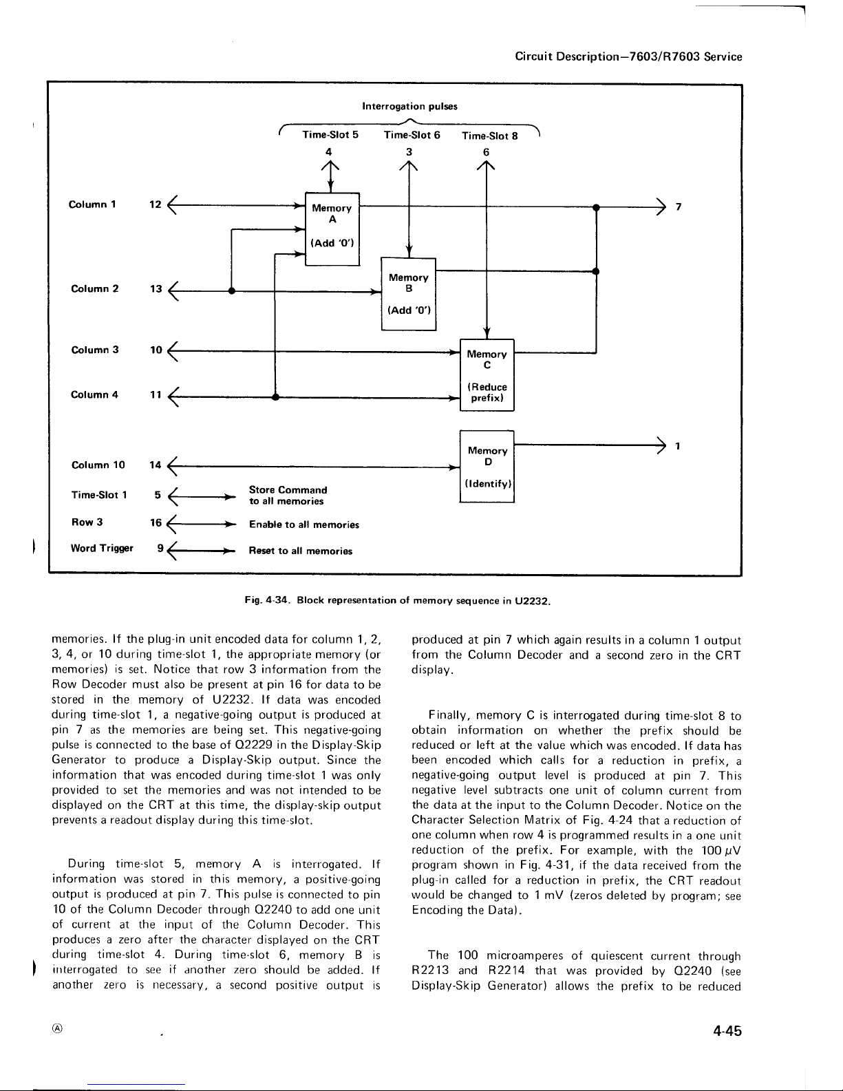
Circuit
Description-7603/R7603
Service
Interrogation
pulses
Time-Slot
6
3
Time-Slot 5
4
Time-Slot
8
6
Column
1
Column 2
Column
3
Column 4
Column
10
Ti m€- Slot 1
Row
3
Word
Trigger
14
5
<---+
:j:T::il}?t.
16
<-+
Enable
to all memories
+-+
Roset
to all
memories
Fig.4-34.
Block representation
of memory
sequence in
U2232.
memories. lf the
plug-in
unit
encoded data for column 1,2,
3,4,
or 10 during time-slot 1, the
appropriate memory
(or
memories) is
set.
Notice
that row 3 information
from the
Row Decoder must
also
be
present
at
pin
16 for
data to
be
stored
in
the memorv
of U2232.
lf
data was encoded
during
time-slot 1, a
negative-going
output
is
produced
at
pin
7
as the
memories
are
being
set.
This
negative-going
pulse
is
connected
to the
base
of Q2229
in
the Display-Skip
Generator
to
produce
a Display-Skip
output. Since the
information
that
was encoded during time-slot 1 was
only
provided
to set the memories
and
was not intended
to be
displayed
on
the CRT
at
this
time, the display-skip
output
prevents
a
readout
display during this time-slot.
During
time-slot 5, memory A is interrogated.
lf
information
was stored in this memory,
a
positive-going
output
is
prodr-rced
at
pin
7. This
pulse
is
connected
to
pin
10
of
the
Column
Decoder
through
02240 to add
one unit
of current
at the
input
of the Column
Decoder. This
produces
a zero after the character
displayed
on the CRT
during time-slot 4. During
time-slot
6, memory B is
irrterrogated
to see
if
another
zero
should be
added. lf
another
zero is necessary,
a
second
positive
output
is
@
produced
at
pin
7 which
again results in
a column 1
output
from
the Column Decoder
and a second
zero in
the CRT
d
isplay.
Finally,
memory C is
interrogated
during
time-slot 8 to
obtain
information
on whether the
prefix
should be
reduced
or left
at
the value
which was
encoded. lf
data has
been
encoded
which calls for a reduction
in
prefix,
a
negative-going
output level is
produced
at
pin
7. This
negative level
subtracts
one unit
of
column
current
from
the data at the input
to the Column Decoder.
Notice
on the
Character
Selection
Matrix
of
Fig. 4 24
that a reduction
of
one column
when
row 4
is
programmed
results in
a one unit
reduction
of the
prefix.
For
example,
with the 1009V
program
shown in Fig. 4
3i,
if
the
data received from
the
plug-in
called for a reduction
in
pref
ix,
the CRT
readout
would be
changed to 1 mV
(zeros
deleted
by
program;
see
Encoding
the Data).
The
100 microamperes
of
quiescent
current
through
R22 13
and R2214 that was
provided
bv
02240
(see
Display-Skip
Generator)
allows the
prefix
to be reduced
4-45
Page 92

Input Pins of Zeros Logic
&
MemorY
Command
Time
Slot
IDENTIFY
I T I qrl q?
| I I
q,
l9
|
DIP
I
q)
|
:l
tPt?
tgtP
t?tPt?t3
tPtPl
OV
TT
204 a
U
12
Add one
zoro
U
Add two
zeros
U
Decrease
prefix
ov
v
Decrease
prefix
and
add one zero
tl
Circu
it Description-7603/R7603
Service
@
4-46
Fi9.zt-35.
Typical outputwaveformsforZerosLogicandMemorystageoperation(atpin7otU2232l.
Page 93

from m
(100
microamperes column
current; column 1) to
no
prefix
(zero
column current; column
zero) so
only
the
unit of
measurement
encoded
during time-slot 9
is
dis-
played.
Notice that reducing the
pref
ix
program
from
column 1 to column
0
programs
the Readout System to not
display a character at
this readout location.
A further feature
of
the Zeros Logic and
Memory is
the
ldentify function. lf 10 units
of
column current are
encoded
by the
plug-in
unit along with
row 3 during
time-slot 1, the Zeros
Logic and
Memory
produces
a
negative-going output
pulse
at
pin
1 which switches the
Column
Data
Switch
and
Row Data Switch to the
ninth
channel. Then,
time-slot
pulses
2 through 9 encode an
output current through resistors
R2191-R2199 for column
data and
R22O1-R2209 for row
data.
This
provides
the
currents
necessary
to display the word
IDENTIFY
on the
CRT
in
the word
position
allotted to the channel which
originated
the ldentify command.
After
completion of this
word, the
Column Data Switch and Row Data Switch
continue with the next word
in
the sequence.
The
Word
Trigger signal from the Word
Trigger stage is
connected
to
pin
9 of U2232 through
C2242. At the end of
each
word of readout
information, this
pulse goes
LO.
This
erases
the four
memories in the Zeros Logic and
Memory in
preparation
for the data
to be received from the
next
channe
l.
Character Generators
The Character Generator stage
consists
of
five similar
integrated circuits U227O,
U2272, U2274, U2276, and
U2278,
which
generate
the
X
(horizontal)
and
Y
(vertical)
outputs at
pins
16
and
1 respectively to
produce
the
character displayed on
the CRT.
Each integrated circuit can
produce
10
individual characters. U227O, which
is desig-
nated
as
the
"Numerals"
Character Generator, can
produce
the
numerals 0
through
9 shown
in
row 1 of the Character
Selection
Matrix
lFig.
424l.
. U2272
can
produce
the
svmbols
shown
in
row 2 of
the Character Selection
Matrix
and U2274
produces
the
prefixes
and some
letters
of
the
alphabet
which are used as
prefixes
in
row
4.
U2216 and
U2278
produce
the
remaining
letters
of
the
alphabet
shown
in
rows 5 and 6 of
the Character Selection
Matrix. All
of
the
stages receive the
column
digital
data from Column
Decoder U2244
in
parallel.
However, only one of the
character
generators
receives
row
data at a
particular
time;
only the
stage which
receives both row
and
column data
is
activated. For example,
if column 2
is
encoded
by
a
plug-in
unit, the
five Character Generators are enabled so that
either a
1,1
p,
V, or an N can
be
produced.
However, if at
the same time
row 4 has also
been
encoded
by the
plug-in
unit, only
the
Prefix Character Generator U2274 will
produce
an output
to result
in
a
pt
displayed on
the screen.
This integrated circuit
provides
current
outputs
to the
Format Generator
which
oroduce
the selected character on
@
Circuit
Description
-7603/R7603
Service
the CRT.
In
a similar
manner,
anv of the
50 characters
shown in
the
Character Selection
Matrix
can be displayed
by
correct
addressing
of the
row
and column.
Decimal
Point
Logic and Character Position
Counter
The Decimal Point Logic
and
Character Position
Counter
stage U2260
performs
two functions. The
first function is
to
produce
a
staircase current which is
added to the X
(horizontal)
signal to space the characters horizontally
on
the CRT.
After
each
character is
generated,
the negative-
going
edge of the Ready signal at
pin
5
advances the
Character
Position
Counter.
This
produces
a
current steo
output at
pin
3
which,
when
added to the X signal, causes
the
next
character to
be
produced
one
character space to
the right. This stage can
also
be advanced when a Space
instruction
is
encoded
by the
plug-in
unit so
that a space
is
left between the displayed characters
on
the CRT. Row 10
information
from the
Row Decoder is
connected to
pin
4
of
U226O through R2265.
When
row 10 and column 0
are
encoded. the output of
this stage
advances one step to
move the next character another space
to the
right.
However,
under this
condition, no
display
is
produced
on
the CRT during this time-slot.
Time-slot
pulses
1
,2,
and 3 are also connected
to
pin
4
of U226O through VR2262, VR2263,
and
VR2264 respec-
tively and R2262-R2265.
This
configuration
adds a space
to the displayed word during time-slots 1,2,
and 3 even
if
information is
not encoded for display
during these
time-slots. With th
is
feature, the information
which is
displayed
during
time-slot4
(1-2-5
data)
always
starts in
the
fourth character
position
whether
data has been displayed
in
the
previous
time-slots or not. Therefore,
the resultant
CRT display does not shift
position
as
normal/invert
or
cal/uncal information is
encoded
by
the
plug-in.
The Word
Trigger
pulse
connected to
pin
8 of U2260 through C2255
resets the Character Position Counter
to the first character
position
at the end
of
each word.
The
Decimal Point Logic
portion
of this stage allows
decimal
points
to
be
added to the CRT display
as encoded
by
the
plug-in
units.
When
row
7 is
encoded
in
coincidence
with columns 3 through
7
(usually
encoded during time-slot
1),
a decimal
point
is
placed
at one of the five locations
on
the CRT
identified in
row 7 of the Character Selection
Matrix
(Fig.
4 24). This instruction
refers
to the decimal
point
location in relation
to the total
number
of
characters
that can be displayed on the CRT
(see
Fig. 4-36). For
example,
if column 3
and
row 7
are encoded during
time-lost 1, the system
is instructed
to
place
a decimal
point
in location No. 3. As shown in Fig. 4-36,
this displays
a decimal
point
before
the th
ird
character that can be
displayed
on
the CRT
(f
irst three time-slots
produce
a space
whether data
is
encoded or
not;
see
previous paragraph).
The
simultaneous application
of
row 7
data to the
Y-input
4-47
Page 94

Decimal-point
location
en-
coded during
this time-sl01
--
no
display
First
possible
character dis-
-z
o.laved
on CRT at this loca-
./
tron
,/
First number
of
measure-
/ /.'/
ment normally displayed at
/ ,/
this location
rr
Decimal
point
location
No.
3
(column
3)
Decimal
point
location
No.
6
(column
6)
Decimal
point
location
No.
5
(column
5)
T T !.tr,T.7
\-->---ll
| \
Always
| | \
skipped
| | \
even
if
/ Decimal ooint \
no
data
/
location
No. 4 \
encoded
7t
(cotumn
4)
\
Circu it
Description-7603/R7603
Service
Fig, 4-36. Readout
word
relating
1O
possible
character locations
to
the decimal-point instructions
that can be encoded
and the resulting
display.
of the Format
Generator through
82280 raises
the decimal
point
so it
appears
between
the displayed
characters.
When
decimal-point
data
is
encoded,
the CRT is
un-
blanked
so a readout
display is
presented.
However,
since
row 7
does
not
activate anv
of the five Character
Generators,
the CRT beam is not
deflected but instead
remains in
a
fixed
position
to display
a decimal
point
between
the characters along
the
bottom
line
of the
readout
word. After the
decimal
point
is
produced
in
the
addressed location,
the CRT beam
returns to
the
location
indicated
by the
Character
Position
Counter
to
produce
the
remainder
of the display.
Format
Generator
The
X
and Y-deflection
signals
produced
by
the
Character
Generator stage,
are connected
to
pins
2
and
7
respectively
of
Format
Generator
U2284. The Channel
Address
No. 2
code from the Channel
Counter
is
also
connected
to
pins
1,8,
and 15
of
this
stage. The Channel
Address
No. 2
code directs the Format
Generator to
add
current to
the X and Y signals
to deflect the CRT
beam to
the area of the
CRT which
;s
associated with the
plug-in
channel
that originated the
information
(see
Fig.
4-24l
.f he
Channel Address
No.2 Code
and the resultant
word
positions
are
shown
in
Table 4-4.
In
addition,
the character
position
current
from
the
Decimal
point
Logic
and Char_
acter Position
stage is
added
to
the X
(horizontal)
input
signal
to space
the characters
horizontally
on the
CRT
(see
previous
discussion).
The Ready
signal
at
pin
13
(coincident
with
Vertical/Horizontal
Channel
Switch
OFF
Command)
activates
this
stage
when a character
is
to be
displayed
on
the CRT.
TABLE
4.4
Channel Address
Y-Output
Amplifiers
The
Y-output signal
at
pin
6 of
U2284
is
connected
to
the Y-Output Amplifier
42287 0'2299. This
stage
provides
a low impedance load
for
the Format
Generator
while
providing
isolation between
the Readout
System
and the
Vertical
Amplifier.
Vertical Separation
adlustment
R22g1
changes
the
gain
of this stage
to control
the
vertical
separation between
the readout
words
displayed
at the
top
and
bottom
of the
graticule
area.
X-Output
Amplifier
The
X-Output
Amplif
ier A2286
02296
operates
simi-
larly
to the
Y-Output
Amplif ier
to
provide
the
horizontal
deflection
from the readout
signal
available
at
pin
4
of
U2284. The
gain
of this stage is
fixed
by the
values
of the
resistors
in the circuit.
Display
Sequence
Fig.
4-37
shows
a flow chart for
the Readout
Svstem.
This
chart
illustrates
the sequence
of events which
occurs
in
the Readout
System each time
a character
is
generated
and
displayed
on the CRT.
(
Channel 1
Left Vertical
Channel
2
Left Vertical
Channel 1
R ight
Vertical
t2
R ight
Vertical
Channel
2
H
ori zontal
4-48
@i
Page 95

Circuit
Description-7603/R7603
Service
5B!
r?i
!u
P
5sE
@
6:
€+
g:a
!(5; i
icYF
xiriE
E
r::
Ed
i h
€ t o
EEE
63f
H €: €
i3;s
F
t(>
c)F
=;z
€ < F n
i
oz 6
:
E:
* := O
; ^;oo
i;sp;
I;:i!
! ts
-vE
tEt
686
F
@
3g
F:,:
5
dsE
!itE
; iF:
6^.
.9
>^.
oFt
=z
P,
o6
E l+>
:!F
.=
cz
o
ou
* F-
.; ai
o.o
xE
q
P4! =
s b=#
; dqo
33BE
9;J
6:6-
!!:3
:!
9
E
oo
^
t
F9
3B!
-< Y
;91
FI;
t
:;o
o
ob
a
Ei:
4-49
Fig-
4-37.
Flow chart
of character generation
sequence
by
rtre
Readout
System.
Page 96

-.t
Page 97

Section
5-7603/R7603
Service
MAINTENAN
CE
This
section
of the manual
contains
maintenance
infor-
mation
for
use in
preventive
maintenance,
corrective
maintenance,
or troubleshooting
of the 7603.
Panel
Removal
WA R'Y''YG
Dangerous
potentials
exist
at several
points
through-
out this instrument.
When
the instrument
is
operated
with
the covers
removed,
do not
touch exposed
connections
or components.
Some transistors
have
voltages
present
on their
cases. Disconnect power
before
cleaning
the instrument
or replacing
parts.
Cabinet Model.
The
side
panels
of the
7603
are
held in
place
by
spring-action
of the
panels
themselves.
To remove
the
panels,
push
the
panel
toward
the
top
of the instrument
until
the bottom
of
the
panel
is
clear
of the
slot
along
the
bottom
rail
of the instrument.
Then,
pull
the
panel
out
at
the
bottom
and lift
away from
the instrument.
The
bottom
panel
is held
in
place
with
eight screws.
The
panels protect
this instrument
from
dust in
the interior,
and
also
provide
protectron
to
personnel
from
the
operating
potentials
present.
They
also
reduce
the EM I
radiation
f
rom
this
instrument
or EMI interference
to
the display
due
to
other
eq u ipment.
I
Rack Model.
The
top cover
is held
in
place
with
six
screws.
To
remove
the
cover,
the screws
need
only be
loosened
slightly to
slide
the cover
out
of the slots.
A
panel
on
the left
side
of the instrument,
held in
place
with
six
screws,
allows
access
to
the vertical
amplifier
circuit
board.
A
plastic
cover
on the rear
of the instrument,
held in
place
with
four
screws,
allows
access
to the
power
supply
regulating
transistors. lt
also allows
access
to three
of
the
five screws
holding
the regulating
circuit
board
assemblv
in
the instrument.
Power-Unit
Removal
The
power
unit can be slid
out of the back
of the 7603
to
gain
access to
the
Logic
and Rectifier
circuit boards
and
for
power-unit
maintenance.
The
power
unit can be left
connected
to the rest
of the
instrument
so that it
can be
operated in
this
position
for
troubleshooting.
To remove
the
power
unit, use the following
procedure:
1. Remove
the side
panels
(top
panel
for
R7603).
2.
Remove
the
five
screws
which secure
the
power
unit
to the sides
of the instrument,
and the
four
rear
panel
screws
(see
Fig.5
1 for locations
of screws
on
R7603).
3.
Slide the
power
unit
out of the rear
of the
instrument
until it can be set
down on the work
surface
(guide
the
I
interconnecting
cables so
they do not catch
on
other
parts
'
of
the instrument)
.
REV.
B, JUNE,1976
{"{
=\,
Fig.
5-1. Power
unit removal for
the
R7603.
PREVENTIVE
MAINTENANCE
General
Preventive
maintenance
consists
of cleaning,
visual
inspection,
lubrication,
etc. Preventive
maintenance
oer-
formed
on a regular
basis
may
prevent
instrument
break-
down
and will improve
the reliability
of this instrument.
The
severity
of
the environment
to
which
the
7603 is
subjected
determines
the frequency
of maintenance.
A
convenient
time
to
perform
preventive
maintenance
is
preceding
recalibration
of the instrument.
Cleaning
The 7603
should be
cleaned
as
often
as operating
conditions
require. Accumulation
of dirt in
the
instrument
can
cause
overheating
and
component
breakdown.
Dirt
on
components
acts
as an insulating
blanket
and
prevents
efficient heat
dissipation.
lt
also
provides
an electrical
conduction
path
which may
result in instrument
failure.
The
side
panels
provide
protection
against dust in
the
interior
of the
instrument.
Operation
without
the
panels
in
place
necessitates
more
f requent
cleaning.
>':::'----s
)
cA u rrorY
(
L'-*(
Avoid
the
use
of chemical
cleaning
agents
which
might
damage
the
plastics
used
in
this instrument.
Avoid
chemicals
which
contain
benzene,
toluene,
xylene,
acetone,
or similar
solvents.
Exterior,
Loose
dust
accumulated
on
the
outside
of the
7603
can
be
removed
with
a soft
cloth
or small
brush.
The
brush
is
particularly
useful
for
dislodging
dirt
on
and
around
the front-panel
controls.
Dirt
which
remains
can
be
removed
with
a soft cloth
dampened
in
a mild
detergent
and
water
solution.
Abrasive
cleaners
should
not
be
used.
5-1
Page 98

Maintena
nce-7603/R 7603
Service
CRT.
Clean the
plastic
light filter,
faceplate
protector,
and the CRT face with a soft, lint-free
cloth
dampened with
denatured alcohol.
The
optional
CRT mesh
filter
can be
cleaned in
the
following
manner:
1. Hold
the mesh
filter in
a vertical
position
and brush
lightly
with a soft No.7
water-color
brush
to remove
liqht
coatings
of dust or lint.
2.
Greasy residues
or dried-on dirt can be removed with
a solution
of
warm water
and a
neutral-pH
liquid
detergent.
Use the brush to lightly scrub the filter.
3. Rinse
the f
ilter
thoroughly
in
clean water
and
allow
to air dry.
4. lf
any
lint
or dirt remains,
use clean low-pressure
arr
to remove
it. Do not
use
tweezers
or other
hard cleaning
tools
on the filter,
as the special
finish may
be
damaged.
5. When not in
use, store the
mesh
filter in a lint-free.
dust-proof container
such as
a
plastic
bag.
Interior.
Dust in
the
interior
of this instrument
should
be
removed
occasionally due to its
electrical conductivity
under
high-humidity
conditions. The best
way to clean
the
interior is
to blow
off
the
accumulated
dust with dry,
low-pressure
air.
Remove
any dirt which
remains with
a soft
brush
or a cloth dampened with
a mild detergent
and water
solution. A cotton-tipped
applicator is
useful for cleaning in
narrow
spaces
or
for cleaning
ceramic
terminal strips
and
circuit boards.
The high-voltage
circuits,
particularly
parts
located
in
the high-voltage compartment
and the
area surrounding
the
post-deflection
anode
lead,
should
receive
special
attention.
Excessive
dirt in
these
areas may
cause
high-voltage
arcing
and result in improper
instrument
operation.
Air Filter
(For
Rackmount Versions
only).
The air filter
should
be visually
checked
every few
weeks
and cleaned
or
replaced
if
dirty. More frequent
inspections
are required
r-rncler
severe
operating conditions.
lf
the filter is
to be
re-
placed,
order
new
filters from
vour
local
Tektronix
Field
Office or representative;
order by
Tektronix Part
No.
378 0041-01
The following
procedure
is
suggested
for
clearrrnq
the filter.
1
Remove the filter
by
pulling
it
out of the retaining
framr:
on the rear
panel.
Be
careful not
to
drop any
ofthe
accumulated
dirt
into
the
instrument.
2. Flush
the loose
dirt from
the filter
r,vith
a stream
of
hot
water.
3.
Place
the filter
in
a solution
of mild cietergent
and hot
water
and
l,rt
soak for
several minutes.
4.
Squert.zi: the f ilter
to wash
out any
cliri which
remains.
5.
Rinse tire f ilter
in
clean water
and ler
dry
5-2
6.
Coat the
dry filter
with
an
air-filter
coating
(available
from
air
conditioner
suppliers
or
order
Tektronix
part
No.
006
0580
00).
7.
Let the
f ilter
thoroughly
dry.
8.
Re-install
the filter
in
the retaininq
frame.
Lubrication
The
reliability
of
potentiometers,
switches,
and
other
moving
parts
can
be maintained
if
they
are kept
properly
lubricated.
However,
over-lubrication
is
as detrimental
as
too little
lubrication.
A lubrication
kit containing
necessary
lubricants
and instructions
is
available
f rom Tektronix.
Inc.
Order Part
No.
003-0342
01.
Visual
Inspection
The
7603
should be inspected
occasionally
for
such
defects
as broken
connections,
improperly
seated
semi-
conductors,
damaged
or
improperly
installed
circuit boards,
and heat-damaged parts.
The
corrective
procedure
for
most
visible
defects is
obvious;
however,
particular
care must
be
taken if
heat-damaged
components
are found.
Overheating
usually indicates
other
trouble in
the instrument;
therefore,
it is important
that
the cause
of overheating
be
corrected
to
prevent
recurrence
of the
damaqe.
Semiconductor
Checks
Periodic
checks
of
the semiconductors
in
the
7603
are
not recommended.
The
best
check
of semiconductor
performance
is
actual
operation in
the
instrument.
More
details
on checking
semiconductor
operation
are
given
under
troubleshooting.
Recalibration
To
assure
accurate
measurements,
check
the
calibration
of this instrument
after
each 1000
hours
of
operation
cr
every
six months
if
used infrequently.
In
addition,
replace-
ment
of components
may
necessitate
recalibration
of
the
affected
circuits. The
calibration procedure
can
also be
helpful
in localizing
certain
troubles in
the instrument.
ln
some
cases,
minor
troubles
may
be
revealed
and/or
corrected
by
recalibration.
TROUBLESHOOTING
Introduction
The
following
information
is
provided
to
facilitate
troubleshooting
of the
7603. Information
contained
in
other
sections
of this manual
should be
used
along with
the
following
information
to
aid in
locating
the
defective
component.
An
understanding
of the circuit
operation
is
very helpful
in locating
troubles,
particularly
where inte-
grated
circu its
are used.
See
the Circuit
Description
section
for
complete
information.
@
Page 99

Troubleshooting
Aids
Diagrams.
Complete
circuit
diagrams are
given
on fold-
out
pages
in
the Diagrams
section. The component
number
and electrical value
of each component
in
this
instrument
are
shown
on these diagrams.
Each main
circuit is
assigned
a
series
of component numbers.
Table
5-1 lists
the main
circuits
in the 7603
and the series
of
componenr
numDers
assigned to each. lmportant
voltages
and
waveforms
are also
shown
on the diagrams. The
portions
of the circuit
mounted
on circuit boards
are enclosed
with blue lines.
Circuit Boards. Fig. 5-2 shows the location
of the
circuit
boards within the
7603; Fig. 5 3
shows the
location
of
circuit boards in the R7603.
Pictures
of
these circuit
boards
are
shown in Figs. 8-1 through 8-10. These
pictures
are located in the Diagrams section
on
the back
of the
page
opposite the
circuit diagram,
to aid the cross-referencing
between
the diagrams and the circuit-board components.
Each
electrical
component
on
the boards is identif ied by its
circuit number.
The
color
and
location
of the
interconnecting connectors are also shown. The circuit boards
are also outlined on
the diagrams with a blue line to show
which
oortions
of the circuit are located on a circuit board.
TABLE 5-1
Component
Numbers
Wiring Color-Code. All insulated
wire
and
cable used in
the
7603 is
color-coded to
facilitate
circuit
tracirrq.
Power
Cord
Conductor
ldentification
Mai
ntenance-7603/R
7603
Service
Resistor
Color-Code.
In
addition to the
brown composi-
tion resistors, some
metal-film resistors and some wire-
wound resistors are
used in the 7603.
The
resistance values
of
wire-wound resistors are
usually
printed
on the body of
the component.
The
resistance
values
of
composition
resistors and
metal-film
resistors
are
color-coded
on
the
components with
EIA color-code
(some
metal-f
ilm
resistors
may have the value
printed
on
the body). The color-code is
read starting with the stripe
nearest the end
of
the resistor.
Composition
resistors have four stripes which
consist
of
two
significant figures, a
multiplier, and a tolerance value
(see
Fig.5-2). Metal-film resistors
have
five stripes
con-
sisting of three
significant figures, a multiplier, and a
tolerance
value.
Capacitor
Marking.
The capacitance
values
of common
disc capacitors
and small
electrolytics
are
marked
on the
side
of the component body. The
white ceramic
capacitors
used in
the 7603
are color-coded in
picofarads
using
a
modif ied EIA
code
(see
Fig.
5-4).
Diode
Color-Code. The
cathode
end
of each
glass-
encased
diode is indicated by
a stripe,
a series
of
stripes,
or
a
dot. For
most silicon or
germanium
diodes
with a series
of
stripes,
the
color-code identifies
the three significant
digits
of the
TE
KTRON
lX
Part Number
using the resistor
color-code system
(e.9.,
a diode color-coded
pink-
or blue-,
brown-gray-green
indicates TEKTRONIX
Part
No.
1520185-00). The cathode
and
anode ends
of
metal-
encased diodes
can be identified bv
the
diode svmbol
marked
on the
bodv.
Semiconductor
Lead Configuration.
Fig.
5-5
shows
the
lead
configuration
for
the semiconductors
used
in
this
instrument.
This
view is
as seen
from the bottom
of the
sem icond
uctors.
Troubleshooting
Equ
ipment
The
following
equipment is
the
7603.
useful
for troubleshooting
1. Transistor
Tester
Description:
TEKTRON
lX Type
576 Transistor-Curve
Tracer
or equivalent.
Component
numbers
on diagrams Circu it
Main Interface
Logic Circuit
Trigger Selector
Vertical I nterface
Vertical Amplif ier
Horizontal
Amplifier
Output Signals
Calibrator
and
Front Panel
1 100-1299 CRT Circuit
and
High Voltage
Low
Voltage
Power
Supply
Readout
System
Alternate
Color
Ungrounded
(Line)
Grounded
(Neutral)
Grounding
(Earthing)
Green-Yellow
Green-Yellow
REV.
C,
AUG.1976
5-3
Page 100

Maintenance-7603/R7603 Service
Fl!
AF
ti
o
.!
(h
<r.
,
o
o
F
0
o
sj
I
E
c
@<
<G
I
E
<U
'F
o
@
5-4
o
FG
FO
a@
\6
;
o
=
.2
x
N
o
:
oo
I
sa
llq
EX
o=
d
Fig.5-2. Location of
circuit boards
in
the 7603.
 Loading...