

Page 1

TM 11-6625-1722-15
TECHNICAL MANUAL
OPE R A TOR ’ S , OR GA N I Z A TI ON A L , D I R E C T S U PPOR T
GE N E R A L S U PPOR T , A N D D E POT M A I N TE N A N CE
MANUAL
OSCI L LOSCOP E AN / U SM - 2 7 3
(NSN 6625-00-930-6637)
This copy is a reprint which includes current
pages from Changes 1.
HEADQUARTERS,
DEPARTMENT OF THE ARMY
JANUARY 1972
Page 2

THIS MANUAL IS AN AUTHENTICATION OF THE MANUFACTURER’S COMMERCIAL LITERATURE WHICH,
THROUGH USAGE, HAS BEEN FOUND TO COVER THE
DATA REQUIRED TO OPERATE AND MAINTAIN THIS
EQUIPMENT. SINCE THE MANIJAL WAS NOT PREPARED
IN ACCORDANCE WITH MILITARY SPECIFICATION, THE
FORMAT HAS NOT BEEN STRUCTURED TO CONSIDER
LEVEL OF MAINTENANCE NOR TO INCLUDE A FORMAL SECTION ON DEPOT MAINTENANCE STANDARDS.
WARNING
DANGEROUS VOLTAGES
EXIST IN THIS EQUIPMENT
DON’T TAKE CHANCES!
CAUTION
Special 3% silver solder is required on the ceramic terminal
strips in this equipment. A 40- to 75-watt soldering iron
should be used and it should be tinned with the same special
solder. Additional quantities of the solder may be procured
under FSN 3439-912-8698. Ordinary solder may be used
only in dire emergency.
Page 3

This Manual Contains Copyrighted Material Reproduced
Tektronix, Inc. All Rights Reserved
Permission Of
By
TM 11-6625-1722-15
T
ECHNICAL M ANUAL
HEADQUARTERS
DEPARTMENT OF THE ARMY
NO. 11–6625–1722–15
ASHINGTON
, D.C., 10 January 1972
W
Operator’s Organizational, Direct Support, General Support, and Depot
Maintenance Manual Including Repair Parts and Special Tools Lists
OSCILLOSCOPE AN/USM–273
S
ECTION A.
INRODUCTION
1.
CHARACTERISTICS
2.
OPERATING INSTRUCTIONS . .. . . . . . . . . . . . . . . . . . . . .
CIRCUIT DESCRIPTION . . . . . . . . . . . . . . . . . .
3.
4.
MAINTENANCE
PERFOR0MANCE CHECK . . . . . . . . . . . . . . . . . . . . .
5.
Page
A-1
1-1
2–1
3–1
4–1
5-1
6.
7.
8.
9.
10,
APPENDIX A .
B.
C.
D.
CALIBRATION
PREVENTIVE MAINTENANCE INSTRUCTIONS . . . . . . . . . . . . . . . . .
MECHNICAL PARTS IDENTIFICATION . . . . . . . . . . . . . . . . . . . . . . .
DIAGRAMS
RACKMOUNTING
REFERENCES
ITEMS COMPRISING AN OPERABLE EQUIPMENT . . . . . . . . . . . . . . . .
MAINTENANCE ALLOCATION . . . . . . . . . . . . . . .
REPAIR PARTS AND SPECIAL TOOLS LIST . . . . . . . . . . . . . .
6–1
7–1
8-1
9-1
10-1
A–1
B–1
C-1
D-1
Page 4

Page 5
TM 11-6625-1722-15
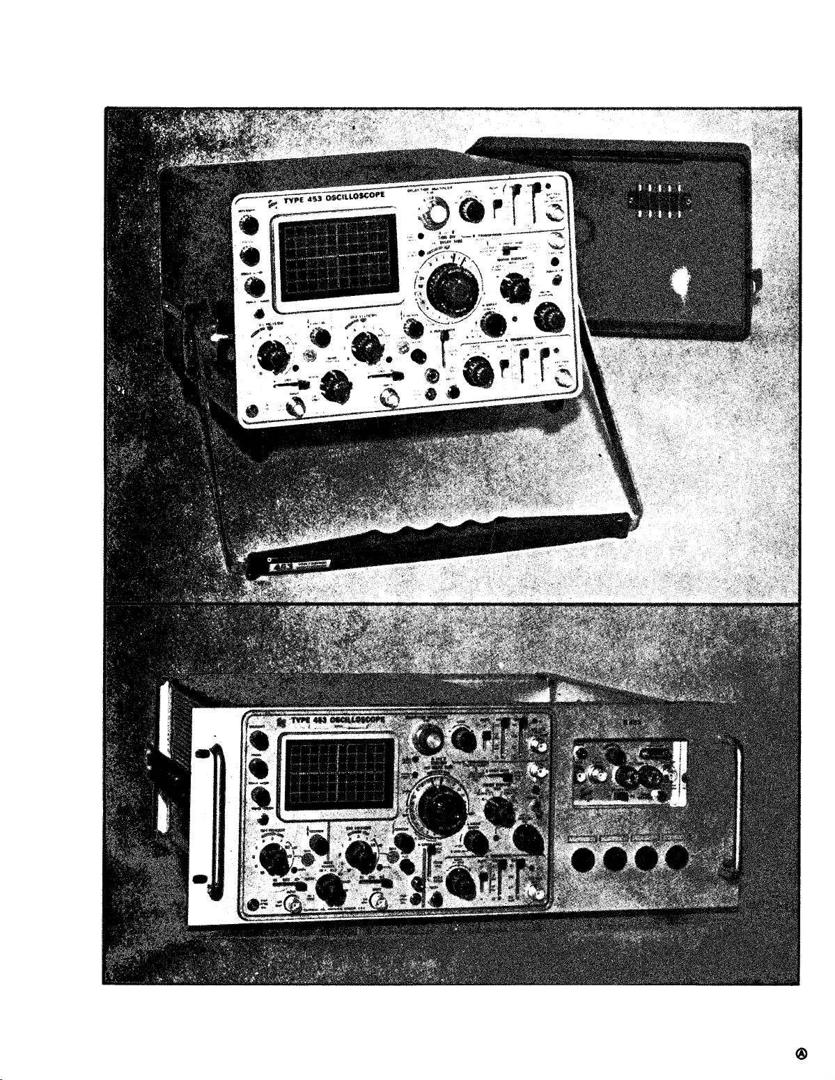
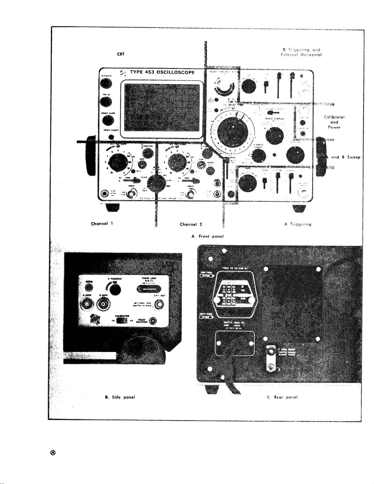
Fig. 1-1. Top; the Type 453 Oscilloscope. Bottom; the Type R453 Oscilloscope.
A-O
Page 6

Page 7

SECTION 0
INSTRUCTIONS
TM 11-6625-1722-15
0-1.
maintenance instructions.
Scope
This manual describes Oscilloscope
Throughout this manual, the AN/USM-273 is re-
AN/USM-273 (fig. 1-1) and provides
ferred to as the Tektronix Type 453 Oscilloscope. The maintenance allo-
cation chart appears in appendix C.
Repair parts and special tools lists
are contained in TM-6625-1722-24P.
0-2.
Indexes of Publications
a. DA Pam 310-4.
Refer to the latest issue of DA Pam 310-4 to deter-
mine whether there are new editions, changes, or additional publications
pertaining to the equipment.
DA Pam 310-7.
b .
Refer to DA Pam 310-7 to determine whether there
are modification work orders (MWO’S) pertaining to the equipment.
0-3.
Maintenance Forms, Records, and Reports
Reports of Maintenance and Unsatisfactory
a.
Equipment.
Department
of the Army forms and procedures used for equipment maintenance will be
those prescribed by TM 38-750, The Army Maintenance Management System.
Report of Packaging and Handling Deficiencies.
b.
Fill out and for-
ward DD Form 6 (Packaging Improvement Report) as prescribed in AR 700-58/
NAVSUPINST 4030.29/AFR 71-13/MCO P4030.29A, and DLAR 4145.8.
Discrepancy
c.
in Shipment Report (DISREP) (SF 361). Fill out and
forward Discrepancy in Shipment Report (DISREP) (SF 361) as prescribed in
AR 55-38/NAVSUPINST 4610.33B/AFR 75-18/MCO P4610.19C and DLAR 4500.15.
0-1
Page 8

TM 11-6625-1722-15
0-4.
Reporting Equipment Improvement Recommendations (EIR)
If your Oscilloscope AN/USM-273 needs improvement, let us know.
You,
us an EIR.
the user,
don’t like about your equipment.
design.
Tell us why a procedure is hard to perform.
(Quality Deficiency Report).
and Electronics Materiel Readiness Command, ATTN:
Monmouth, NJ 07703.
0-5.
Administrative Storage
We’ll send you a reply.
are the only one who can tell us what you
Let us know why you don’t like the
Put it on an SF 368
Mail it to Commander, US Army Communications
DRSEL-ME-MQ, Fort
Administrative storage of equipment issued to and used by Army activi-
ties shall be in accordance with TM 740-90–1.
0-6
Destruction of Army Electronics Materiel
Destruction of Army electronics materiel to prevent enemy use shall be
Send
in accordance with TM 750-244-2.
0-7.
Reporting Errors and Recommending Improvements
You can help improve this manual. If you find any mistakes or if you
know of a way to improve the procedures, please let us know. Mail your
letter or DA Form 2028 (Recommended Changes to Publications and Blank
Forms) to
Readiness Command, ATTN:
either case,
Commander, US Army Communications and Electronics Materiel
DRSEL-ME-MQ, Fort Monmouth, NJ 07703. In
a reply will be furnished direct to you.
0-2
Change 1
Page 9

SECTION 1
CHARACTERISTICS
TM 11-6625-1722-15
Introduction
The Tektronix Type 453 Oscilloscope is a transistorized
portable oscilloscope designed to operate in a wide range
of environmental conditions. The light weight of the Type
453 allows it to be easily transported, while providing the
performance necessary for accurate high-frequency measurements.
provides calibrated deflection factors from 5 millivolts to
10 volts/division. Channels 1 and 2 can be cascaded using
an external cable to provide a one millivolt minimum defection factor (both VOLTS/DIV switches set to 5 mV).
The trigger circuits provide stable triggering over the full
range of vertical frequency response. Separate trigger controls are provided to select the desired triggering for the A
and B sweeps. One of three sweep modes can be selected
for the A sweep; automatic, normal or single sweep. The
horizontal sweep provides a maximum sweep rate of 0.1
microsecond/division (10 nanosecond/division using 10X
magnifier) along with a delayed sweep feature for accurate
relative-time measurements.
can be made with Channel 2 providing the vertical deflection,
and Channel 1 providing the horizontal [deflection. (TRIGGER
switch set to CH 1 ONLY, HORIZ DISPLAY switch set to EXT
HORIZ). The regulated DC power supplies maintain con-
The dual-channel DC-to-50 MHz vertical system
Accurate X-Y measurements
ELEC TRI C A L C H A RA C TERI STI C S
VERTICAL DEFLECTlON SYSTEM
stant output over a wide variation of line voltages and frequencies.
approximately 90 watts.
Information given in this instruction monual applies to the
Type R453 also unless otherwise noted. The Type R453 is
electrically identical to the Type 453 but is mechanically
adapted for mounting in a standard 19-inch rack. Rackmounting instructions, a mechanical parts list and a dimensional drawing for the Type R453 are provided in Section
10 of this manual.
The electrical characteristics which follow are divided
into two categories. Characteristics listed in the Performance
Requirement column are checked in the Performance Check
and Calibration sections of this manual. Items listed in the
Operational Information column are provided for reference
use and do not directly reflect the measurement capabilities of this instrument. The Performance Check procedure
given in Section 5 of this manual provides a convenient
method of checking the items listed in the Performance
Requirement column. The following electrical characteristics
apply over a calibration interval of 1000 hours at an ambient temperature range of -15°C to +55°C, except as
otherwise indicated. Warm-up time for given accuracy is
20 minutes.
Total power consumption of the instrument is
. .
Characteristic
Deflection Factor
Deflection Accuracy
Variable Deflection Factor
Bandwidth at Upper -3 dB
point (with or without P6010
Probe)
20 mV to 10 VOLTS/DIV
10 mV/DIV
5 mV/DIV
Channels land 2 cascaded
Risetime (calculated). With or
without P6010 Probe.
20 mV to 10 VOLTS/DIV
10 mV/DIV
5 mV/DIV
Channels 1 and 2 cascaded
Performance Requirement
5 millivolts/division to 10 volts/division in 11
calibrated steps for each channel. One millivolt/
division when Channel 1 and 2 are cascaded.
Within ±3Y% of indicated deflection with VARlABLE control set to CAL. Cascaded deflection
factor uncalibrated.
Uncalibrated deflection factor at least 2.5 times
the VOLTS/DIV switch indication. This provides
a maximum uncalibrated deflection factor of 25
volts/division in the 10 volts position.
DC to 50 MHz or greater
DC to 45 MHz or greater
DC to 40 MHz or greater
DC to 25 MHz or greater
Less than 7 nanoseconds
Less than 7.8 nanoseconds
Less than 8.75 nanoseconds
Less than 14 nanoseconds
Operational Information
Steps in 1-2-5 sequence
With gain correct at 20 mV
Driven from 25-ohm source
Measured at one millivolt/division
Risetime calculated from bandwidth
measurement using the formula:
Where:
= Risetime in nanoseconds.
t
r
BW = Bandwidth in megahertz.
1-1
Page 10

TM 11-6625-1722-15
Characteristic
Input RC Characteristics
Maximum lnput Voltage
lnput Coupling Modes
AC Low-Frequency Response
(lower -3 dB point)
Without probe
With P6010 Probe
Trace Shift Due to Input Gate
Current (at 25°C)
Vertical Display Modes
Chopped Repetition Rate
Attenuator Isolation
Common Mode Rejection Ratio
Linear Dynamic Range Useful
for Common-Mode Relection
in ADD Mode
Polarity Inversion
Signal Delay Line
Low-Frequency
Vertical Linearity
Trace Drift (after 20 minute
warm up)
20 mV to 10 VOLTS/DIV
10 mV/DIV
5 mV/DIV
VERTICAL (cont)
Performance Requirement
AC or DC, selected by front-panel switch
Negligible
Channel 1 only
Channel 2 only
Dual-troce, alternate between channels
Dual-trace, chopped between channels
Added algebraically
Approximately one-microsecond segments from
each channel dispiayed at repetition rate of 500
kHz, ±20%.
Greater than 10,000:1, DC to 20 MHz
Greater than 20:1 at 20 MHz for common-mode
signals less than eight times VOLTS/DIV switch
setting.
Signal on Channel 2 can be inverted
Less than 0.15 division compression or expansion
of two division signal when positioned to vertical
extremes of display area
Operational Information
Typically 1 megohm (±2%), paralleled
by 20 pF (±3%)
600 volts DC + peak AC (one kilohertz
or less). Peak-to-peak AC not to exceed
600 volts.
Typicaily 1.6 Hz, Input Coupling switch
set to AC
Typically 0.16 Hz
With optimum GAIN
frequency
Less than 10% incremental signal dis-
tortion for instantaneous input voltage
-10 or +10 times VOLTS/DIV
of
switch setting
Approximately 140 nanoseconds
Includes CRT linearity. Measured with
one-kilohertz square wave.
Time
Typically less than Typically less than
0.03 division/hour
Typically less than
0.05 division/hour
Typically less than
0.08 division/hour
adjustment at low
Temperature
0.0075 division/degree C
Typically less than
0.0125 division/degree C
Typically less than
0.02 division/de-
gree C
Source
Coupling
Polarity
1-2
TRIGGERING (A AND B SWEEP)
Internal from displayed channel or from Channel
1 only
Internal from AC power source
External
External divide by 10
AC
AC low-frequency reject
AC high-frequency reject
DC
Sweep can be triggered from positive-going or
negative-going portion of trigger signal
Page 11

TRIGGERING (cont)
TM 11-6625-1722-15
Characteristic
Internal Trigger Sensitivity
AC
LF REJ
HF REJ
DC
External Trigger Sensitivity
AC
LF REJ
HF REJ
DC
Auto Triggering (A sweep only)
Single Sweep (A sweep only)
Display Jitter
Maximum Input Voltage
External Trigger Input RC
Characteristics (approximate)
LEVEL Control Range
Performance Requirement
0.2 division of deflection, minimum, 30 Hz to 10
MHz; increasing to 1 division at 50 MHz
0.2 division of deflection, minimum, 30 Hz to 10
0.2 division of deflection, minimum, 30 kHz to 10
0.2 division of deflection, minimum, 30 Hz to 50
kHz
0.2 division of deflection, minimum, DC to 10
MHz; increasing to 1 division at 50 MHz
50 millivolts, minimum, 30 Hz to 10 MHz; increasing to 200 millivolts at 50 MHz
50 millivolts, minimum, 30 kHz to 10 MHz; increasing to 200 millivolts at 50 MHz
50 millivolts, minimum, 30 Hz to 50 kHz
50 millivolts, minimum, DC to 10 MHz; increas-
ing to 200 millivolts at 50 MHz
Stable display presented with signal amplitudes
given under Internal and External Trigger Sensitivity above 20 Hz. Presents a free-running sweep
for lower frequencies or in absence of trigger
signal.
A Sweep Generator produces only one sweep
when triggered. Further sweeps are locked out
until RESET button is pressed. Trigger sensitivity
same as given above.
Less than 1 nanosecond at 10 nanoseconds/division sweep rate (MAG switch set to X10)
At least ±2 volts, SOURCE switch in EXT position. At least ±20 volts, SOURCE switch in EXT
÷10 position
Operational Information
Typical -3 dB point, 16 Hz
Typical -3 dB point, 16 kHz
Typical -3 dB points, 16 Hz and 100
kHz
Typical -3 dB point, 16 Hz
Typical -3 dB point, 16 kHz
Typical -3 dB points, 16 Hz and 100
kHz
600 volts DC + peak AC (one kilohertz
or less). Peak-to-peak AC not to exceed
600 volts.
1 Megohm paralleled by 20 pF, except
in LF REJ
Sweep Rates
A Sweep
B sweep
Sweep Accuracy-A and B
Sweep
5 s to 0.1 s/DIV
50 ms to 0.1 µs/ DIV
Variable Sweep Rate
HORIZONTAL DEFLECTION SYSTEM
A and B Sweep Generator
0.1 microsecond/division to 5 seconds/division in
24 calibrated stem
0.1 microsecond/division to 0.5 second/division
in 21 calibrated steps
0°C to +40°C
Within ±3% of indi- Within ±5% of indi-
cated sweep rate
Within ±3% of indi- Within ±4% of indi-
cated sweep rate
Uncalibrated sweep rate to at least 2.5 times the
TIME/DIV indication, or a maximum of at least
12.5 seconds/division in the 5 s position (B sweep,
maximum of 1.25 seconds/division in the .5 s
position.
-15°C to +55°C
cated sweep rate
cated sweep rate
A sweep is main and delaying sweep
B sweep is delayed sweep
A VARIABLE and B TIME/DiV VARlABLE controls set to CAL
1-3
Page 12
TM 11-6625-1722-15
A and B Sweep Generotor
Characteristic
Sweep Length
A sweep
B sweep
Sweep Hold-off-A sweep
5s to 10
Sweep Magnification
Magnified Sweep Accuracy 1% tolerance added to speclfled sweep accuracy
Magnified Sweep Linearity
Normal/Magnified Registration
Calibrated Delay Time Range
DELAY-TIME MULTIPLIER
Dial Range
Delay Time Accuracy
5s to 0.1 s/DIV
50 ms to 1
Incremental Multiplier Linearity
Delay Time Jitter
Variable from less than 4 divisions to 11.0, ±0.5
division
11.0 divisions, ±0.5 division
Less than one times the A TIME/DIV switch set-
ting
Less than 2.5 microseconds
Each sweep rate can be increased 10 times the Extends fastest sweep rate to 10 nano-
indicated sweep rate by horizontally expanding seconds/division
the center division of display
±1.5% for any eight division portion of the
total magnified sweep length (excluding first
and last 60 nanoseconds of magnified sweep)
±0.2 division, or less, trace shift at graticuie
center when switching MAG switch from X10
to OFF
Continuous from 50 seconds to 1 microsecond A VARIABLE control set to CAL for indi-
0.20 to 10.20
0°C to +40°C -15° C to +55° C
Within ±2.5% of indicated delay cated delay Includes incremental multiplier linearity
Within ±1.5% of indicated delay cated delay
±0.2%
Less than 1 part in 20,000 of 10 times A TIME/
DIV switch setting
Performance Requirement
Sweep Magnifier
Sweep Delay
Within ±3.5% of indi-
‘Within ±2% of indi-
±0.3%.
Operational Information
A TIME/DIV switch set to 1 ms
B TIME/DIV switch set to 1 ms
cated delay
Equal to 0.5 division, or less, with the A
TIME/DIV switch set to 1 ms and the B
TIME/DIV switch set to 1
Input to Channel 1 (TRIGGER
switch in CH 1 ONLY)
Deflection factor
Accuracy
X Bandwidth at Upper -3 dB
Point
Input RC characteristics
Phase difference between X
and Y amplifiers at 50 kHz
Input to EXT HORIZ Connector
Deflection factor
1-4
External Horizontal Amplifier
5 millivolts/division to 10 volts/division in 11 calibrated steps
0°C to +40°C
Within ±5% of indi- Within ±8% of indi-
cated deflection
5 MHz or greater
Less than 3°
B SOURCE switch in EXT; 270 millivolts/division,
±15%.
B SOURCE switch in EXT
±20%
cated deflection
Steps in 1-2-5 sequence.
Channel 1 VARIABLE control does not
affect horizontal deflection
With external horizontal gain correct
at 20 mV
Typically 1 megohm (±2%), paralleled
by 20 pF (±3%)
Page 13

Ex t e r na l H o r iz o n ta l A m p l i fi e r (c ont)
X Ba nd w id th a t Up p er -3 5 M Hz o r g re a te r
TM 11-6625-1722-15
Operational Information
—
Input RC c h ara c te ristic s
(approxima te]
Ph a se d if fe re n c e b etw e e n X
and Y amplifiers at 50kHz
CALIBRATOR
Waveshap e
Po la rit y
Output Voltage
Output Current
Sq u a r e w a v e
Po sit ive g o in g w it h b a se line a t ze ro v o lt s
0.1 vo lt o r 1 volt, p ea k to p eak
5-milliamp ere s through PROBE LOO P on side
Re p e t i t i o n Ra t e
Volta ge Accuracy
Current Accuracy
Re p e t it i o n Ra t e A c c u r a c y
Ri se t im e
Duty C ycIe
.-
±1.5%
±0.5%
Le ss t ha n 1 m ic r o se c o n d
49% to 51%
Output Resistance
Z A XI S I NPUT
Se n s i t i v i t y
5 v olt p ea k-to-p ea k signal p rod uc e s no tic e able
modulation
Usa b le Freq ue n c y Ra ng e D C t o g re ate r t ha n 50 M Hz
Input Re sista nc e a t DC
Input C o up ling DC coupled
Po la rity o f O p e ra tio n
1 me gohm, para llele d by 20 pF
Le ss t h a n 3 °
Selected by CALIBRATOR switch on side
panel
Approximately 200 ohms in 1 V position.
Approximately 20 ohms in .1 V position.
Approximately 47 kilohms
Po sitiv e-g o in g inp u t sig n a l d e c re a se s
trac e intensity
Neg ative-g oing signal inc rea ses trace
Maximum Input Voltage
A and B Ga te
Waveshap e
Amplitude
Po la rity
Duration
Output resistance
Vertica l Signal Out (CH 1 only)
Output voltage
Ba n d w id t h
Output coupling
Output resistance
O UTPUT SIGN ALS
—
Re c t a n g u l a r p u l se
Po slt lve-g o in g w it h b a se line a t a b o u t - 0.7 v o lt s.
I Same d ura tio n a s the re sp ec t ive sw eep
I
25 m illivo lts, o r g rea ter/ division o f CRT d isplay
int o 1 meg oh m load .
DC to 25 MHz or g rea te r when ca sca ded with
Channel 2 or into 50-ohm load.
DC coup led
200 vo lts c om bined DC and pea k AC
A GATE duration variable between
about 4 and 11 times the A TIME/DIV
sw i tc h se t t in g
with the A SWEEP
LENG TH c o n t ro l .
Approximately 1.5 kilohms
Approximately 50 ohms
1-5
Page 14

TM 11-6625-1722-15
Characteristic
Line Voltage
Voltage Ranges (AC, RMS)
115-volts nominal
230-volts nominal
Line Frequency
Maximum Power Consumption
at 115 Volts, 60 Hz
Tube Type
Phosphor
Accelerating Potential
Graticule
Type
Area
Illumination
Unblinking
Raster Distortion
Trace Finder
POWER SUPPLY
Performance Requirement
115 volts nominal or 230 volts nominal
90 to 110 volts
104 to 126 volts
112 to 136 volts
180 to 220 volts
208 to 252 volts
224 to 272 volts
———
48 to 440 Hz
CATHODE-RAY TUBE (CRT)
I
Internal
Six divisions vertical by 10 divisions horizontal.
Each division equals 0.8 centimeter.
0.1 division or less total
Limits display within graticule area when pressed.
Operational Information
.—
Line voltage and range selected by Line
Voltage Selector assembly on rear
panel. Voltage ranges apply for waveform distortion which does not reduce
the peak line voltage more than 5%
below the true sine-wave peak value.
92 watts (105 volt-amperes)
Tektronix T4530-31-1 rectangular
P31 standard. Others available on
special order.
Approximately 10 kV total (cathode
potential -1.95 kV).
Variable edge lighting
Bias-type, DC coupled to CRT grid.
Adjustable with Geometry and Y Axis
Align adjustments.
Characteristic
Temperature
Operating
Non-operating
Altitude
Operating
Non-operating
Humidity
Non-operating
Vibration
Operating and
non-operating
Shock
Operating and
non-operating
ENVIRONMENTAL CHARACTERISTICS
The following environmental test limits apply when tested in accordance with the recommended test procedure. This instrument will meet the electrical characteristics given in this
section following environmental test.
including failure criteria, etc., may be obtained from Tektronix, Inc. Contact your local
Tektronix Field Office or representative.
Performance Requirement
-15°C to +55°c
-55° to +75°C
15,000 feet maximum
50,000 feet maximum
Five cycles (120 hours) of Mil-Std-202C, Method
106B
15 minutes along each of the three major axes
at a total displacement of 0.025-inch peak to peak
(4 g at 55 c/s) with frequency varied from 10-5510 c/s in one-minute cycles. Hold at 55 c/s for
three minutes on each axis.
Two shocks of 30 g, one-half sine, 11 millisecond
duration each direction along each major axis.
Complete details on environmental test procedures,
Supplemental Information
Fan at rear circulates air throughout instrument.
cutout protects instrument from overheating.
Derate maximum operating tempera-
ture by 1°C/1000 feet change in altitude
above 5000 feet.
Exclude freezing and vibration
Instrument secured to vibration platform
during test. Total vibration time, about
55 minutes.
Guillotine-type shocks.
Total of 12 shocks
Automatic resetting thermal
1-6
Page 15

EN V I RO N M EN TA L C HARAC TERI STIC S (c ont)
TM 11-6625-1722-15
Characteristic
Tr a n s p o r t a t i o n
Pa c ka g e v ib ra t io n
Pa c ka g e d ro p
Ty p e 4 5 3
Ty p e R 4 5 3
MECHANICAL CHARACTERISTICS
Characteristic
Construction
Chassis
Pa n el
Cabinet
Circuit boards
Overall Dimensions, Type
453 (m easured ot m aximum points)
He ig ht
Width
Le n g t h
Overall Dimensions, Type
R4 53 ( m e a su r e d a t m a x imum points)
He ig ht
Pe rf orm a nc e Re q u ire m e nt
Meets National Safe Transit type of test when
packaged as shipped from Tektronix, Inc.
One hour vibration slightly in excess of 1 g.
30-inc h drop o n any corne r, e dge o r fla t surface.
18-inc h drop on a ny c orner, e d ge or fla t surface.
Width
Info rmation
Le n g t h
Aluminum alloy
Aluminum alloy with ano-
dized finish
Blu e v in y l- c o a t e d a l um i n um
Glass-epoxy laminate
Connectors
Z A XIS I NP UT
All other connec tors
Net Weight
Ty p e 4 5 3 ( i n c l u d e s f r o n t
cover without accessor-
Ty p e R 4 5 3 ( w i t h o u t a c -
hand le positioned for ca rrying .
St a n d a r d a c c e s so r i e s s u p p l i e d w i t h t h e Ty p e 4 5 3 a n d R4 5 3
are listed on the last pullout page of the Mechanical Parts
List illu st ra t io ns.
7 inches
Operational Information
Pa c ka ge sho uld just l ea ve vib ra t io n surface
19 inc hes
panel;
Bin d i ng p o st
BN C
Approximately 29 pounds.
ies)
Approximately 32 pounds.
cessories)
STANDA RD A C C ESSO RIES
1-7
Page 16

Page 17
SECTION 2
OPERATING INSTRUCT IONS
General
O effectively use the Type 453, the operation and capa-
T
bilities of the instrument must be known. This section describes the operation of the front-, side- and rear-panel
controls and connectors, gives first time and general operating information and lists some basic applications for this
instrument.
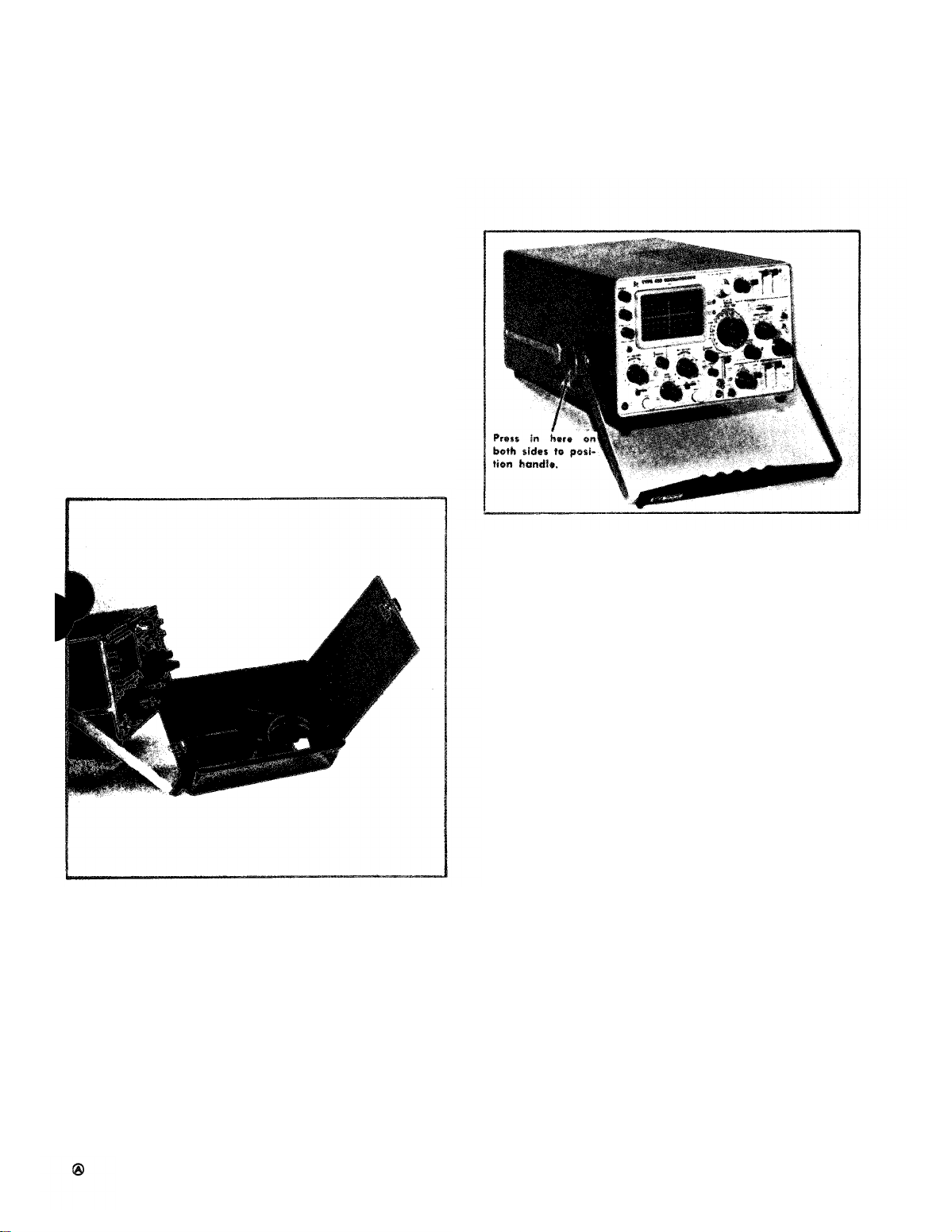
Front Cover and Handle
The front cover furnished with the Type 453 provides a
dust-tight seal around the front panel. Use the cover to
protect the front panel when storing or transporting the
instrument. The cover also provides storage space for probes
and other accessories (see Fig. 2-1).
TM 11-6625-1722-15
Fig. 2-1. Accessory storage provided in front cover.
The handle af the Type 453 can be positioned for carrying
or as a tilt-stand for the instrument. To position the handle,
press in at both pivot points (see Fig. 2-2) and turn the
handle to the desired position. Several positions are provided for convenient carrying or viewing. The instrument
may also be set an the rear-panel feet for operation or
storage.
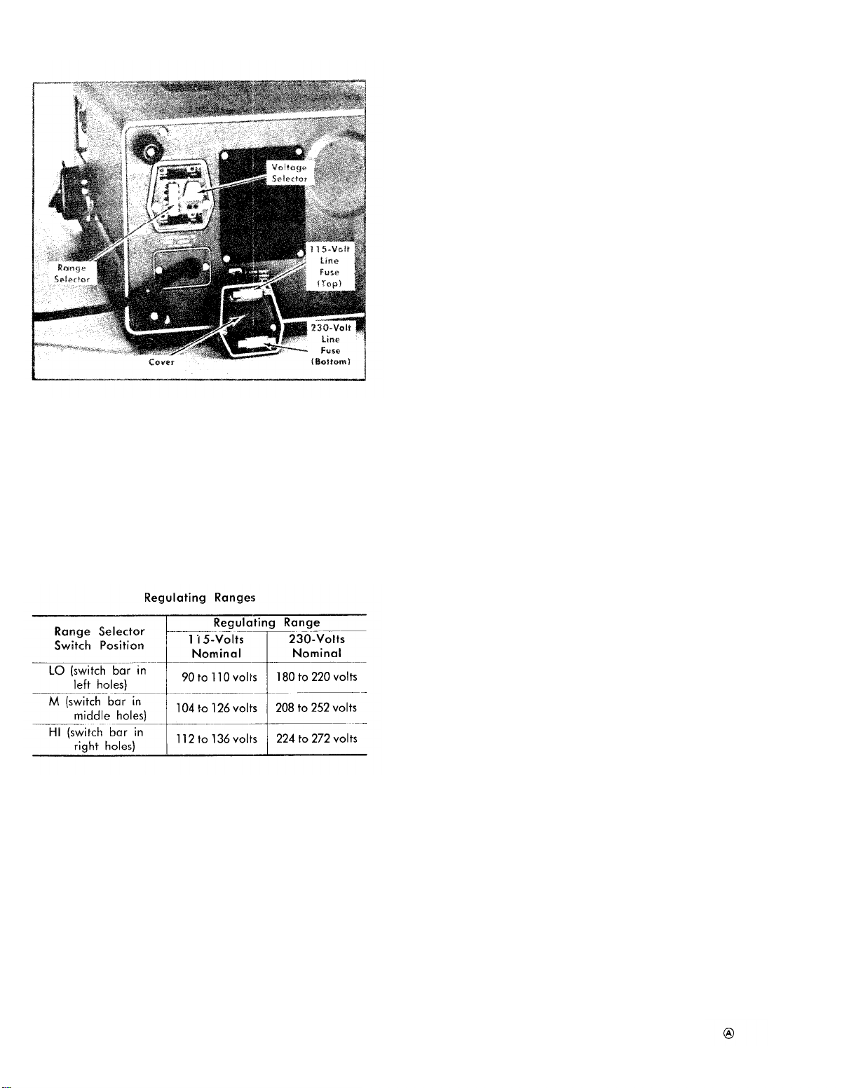
Operating Voltage
The Type 453 can be operated from either a 115-volt or
a 230-volt nominal line-voltage source. The Line Voltage
Fig. 2 -2 . Handle positione d to provide a sta nd for t he instrum ent
Selector assembly on the rear panel converts the instrument
from one operating range to the other. In addition, this
assembly changes the primary connections of the power
transformer to allow selection of one of three regulating
ranges. The assembly also includes the two line fuses. When
the instrument is converted from 115-volt to 230-volt nominal
operation, or vice versa, the assembly connects or disconnects one of the fuses to provide the correct protection for
the instrument. Use the following procedure to convert this
instrument between nominal line voltages or regulating
ranges.
1. Disconnect the instrument from the power source.
2. Loosen the two captive screws which hold the cover
onto the voltage selector assembly; then pull to remove the
cover.
3. To convert from 115-volts nominal to 230-volts nominal line voltage, pull out the Voltage Selector switch bar
(see Fig. 2-3]; turn it around 180° and plug it back into the
remaining holes. Change the line-cord power plug to match
the power-source receptacle or use a 115- to 230-volt
adapter.
4. To change regulating ranges, pull out the Range
Selector switch bar (see Fig. 2-3); slide it to the desired
position and plug it back in. Select a range which is centered about the average line voltage to which the instrument is to be connected (see Table 2-1).
5. Re-install the cover and tighten the two captive screws.
6. Before applying power to the instrument, check that
the indicating tabs on the switch bars are protruding through
the correct holes for the desired nominal line voltage and
regulating range.
2-1
Page 18
TM 11-6625-1722-15
Fig. 2-3. Line Voltage Selector assembly on the rear panel (shown
with cover removed).
CAUTION
The Type 453 should not be operated with the
Voltage Selector or Range Selector switches in the
wrong positions for the line voltage applied.
Operation of the instrument with the switches in
the wrong positions may either provide incorrect
aperotion or damage the instrument.
TABLE 2-1
more frequently. The air filter should be cleaned occasion-
ally to aII
OW the maximum amount of cooling air to enter
the instrument. Cleaning instructions are given in Section 4.
The Type 453 can be operated where the ambient air
temperature is between
-15°C and +55°C. Derate the
maximum operating temperature 1°C for each additional
1000 feet of altitude above 5000 feet. This instrument can
be stored in ambient temperatures between –55°C and
+75°C. After storage at temperatures beyond the operating
limits, allow the chassis temperature to come within the
operating limits before power is applied.
Rackmounting
Complete information for mounting the Type R453 in a
cabinet rack is given in Section 10 of this manual.
CONTROLS AND CONNECTORS
A brief description of the function or operation
front-, side- and rear-panel controls and connectors
(see Fig. 2-4). More detailed information is given
of the
follows
in this
section under General Operating Information.
Cathode-Ray Tube
INTENSITY
FOCUS
Controls brightness of display.
Provides adjustment for a well-defined display.
SCALE ILLUM
TRACE FINDER
Controls graticule illumination.
Compresses display within graticule area
independent of display position or applied signals.
Operating Temperature
The Type 453 is cooled by air drawn in at the rear and
blown out through holes in the top and bottom covers. Adequate clearance on the top, bottom and rear must be provided to allow heat to be dissipated away from the instru-
ment. The clearance provided by the feet at the bottom and
rear should be maintained. If possible, allow about one
inch of clearance on the top. Do not block or restrict the air
flow from the air-escape holes in the cabinet.
A thermal cutout in this instrument provides thermal protection and disconnects the power to the instrument if the
internal temperature exceeds a safe operating level. Operation of the instrument for extended periods without the covers
may cause it to overheat and the thermal cutout to open
Vertical (both
VOLTS/DIV
VARIABLE
UNCAL
POSITION
GAIN
Input Coupling
(AC GND DC)
channels except as noted)
Selects vertical deflection factor (VARlABLE control must be in CAL position for
indicated deflection factor).
Provides continuously variable deflection
factor between the calibrated settings of
the VOLTS/DIV switch.
Light indicates that the VARIABLE control
is not in the CAL position.
Controls vertical position of trace.
Screwdriver adjustment to set gain of the
Vertical Preamp. Line between adjustment and 20 mV VOLTS/DIV position indicates that gain should be set with
VOLTS/DIV switch in this position.
Selects method of coupling input signal
to Vertical Deflection System.
AC: DC component of input signal is
blocked. Low frequency limit -3 dB
point) is about 1.6 hertz.
GND: Input circuit is grounded (does not
ground applied signal).
2-2
Page 19
TM 11-6625-1722-15
Fig. 2-4. Front-, side- and rear-panel controls and connectors.
2-3
Page 20

TM 11-6625-1722-15
DC: All components of the input signal are
passed to the Vertical Deflection System.
STEP ATTEN
BAL
INPUT
MODE
TRIGGER
INVERT (CH 2
only)
A and B Triggering (both where applicable)
EXT TRIG
INPUT
SOURCE
Screwdriver adjustment to balance Vertical Deflection System in the 5, 10 and 20
mV positions of the VOLTS/DIV switch.
Vertical input connector for signal.
Selects vertical mode of operation.
CH 1: The Channel 1 signal is displayed.
CH 2: The Channel 2 signal is displayed.
ALT: Dual trace display of signal on both
channels. Display switched at end of
each sweep.
CHOP: Dual trace display of signal on
both channels. Approximately one-microsecond segmerlts from each channel
displayed at a repetition rate of about
500 kilohertz.
ADD: Channel 1 and 2 signals are alge-
braically added and the algebraic sum
is displayed on the CRT.
Selects saurce of internal trigger signal
from vertical system.
NORM: Sweep circuits triggered from dis-
played channel(s). Channel 1 signal
available at CH 1 OUT connector.
CH 1 ONLY: Sweep circuits triggered only
from signal applied to the Channel 1
INPUT connector. No signal available
at CH 1 OUT connector. CH 1 lights,
located beside A and B SOURCE switches indicate when the TRIGGER switch is
in the CH 1 ONLY position.
Inverts the Channel 2 signal when pulled
out.
Input connector for external trigger signal.
Connector in B Triggering section of front
panel also serves as external horizontal
input when HORIZ DISPLAY switch is in
EXT HORIZ position and B SOURCE switch
is in EXT position.
Selects source of trigger signal.
INT: Internal trigger signal obtained from
Vertical Deflection System. When CH
1 light is on, trigger signal is obtained
only from the Channel 1 input signal;
when the light is off, the trigger signal
is abtained from the displayed chan-
nel(s). Source of internal trigger signal
is selected by the TRIGGER switch.
LINE: Trigger signal obtained from a sam-
ple of the line voltage applied to this
instrument.
EXT: Trigger signal obtained from an ex-
ternal signal applied to the EXT TRIG
INPUT connector.
nal approximately 10 times.
CH 1
COUPLING
SLOPE
LEVEL
HF STAB Decreases display jitter for high-frequency
(A Triggering only) sweep rates.
A and B Sweep
DELAY-TIME
MULTIPLIER
A SWEEP
TRIG’D
UNCAL A
OR B
A AND B
TIME/DIV
AND DELAY
TIME
Light indicates that the internal trigger signal is abtained only from the signal connected to the Channel 1 INPUT connector
(see TRIGGER switch).
Determines method of coupling trigger
signal to trigger circuit.
AC: Rejects DC and attenuates signals be-
low about 30 hertz. Accepts signals
between abaut 30 hertz and 50 megahertz.
LF REJ: Rejects DC and attenuates signals
below about 30 kilohertz. Accepts signals between about 30 kilohertz and 50
megahertz.
HF REJ: Accepts signals between about 30
hertz and 50 kilohertz; rejects DC and
attenuates signals outside the above
range.
DC: Accepts all trigger signals from DC to
50 megahertz or greater.
Selects portion of trigger signal which
starts the sweep.
+: Sweep can be triggered from positive-
going portion of trigger signal.
-: Sweep can be triggered from negativegoing portion of trigger signal.
Selects amplitude point on trigger signal
at which sweep is triggered.
signals. Has negligible effect at lower
Provides variable sweep delay between
0.20 and 10.20 times the delay time indi-
cated by the A TIME/DIV switch.
Light indicates that A sweep is triggered
and will produce a stable display with
correct INTENSITY and POSITION control
settings.
Light indicates that either the A or B
VARIABLE control is not in the CAL posi-
tion.
A TIME/DIV switch (clear plastic flange)
selects the sweep rate of the A sweep
circuit for A sweep only operatian and
selects the basic delay time (to be multi-
plied by DELAY-TIME MULTIPLIER dial
setting) for delayed sweep operation.
B TIME/DIV (DELAYED SWEEP) switch
selects sweep rate of the B sweep circuit
Attenuates external trigger sig-
2-4
Page 21

TM 11-6625-1722-15
A VARIABLE
B SWEEP
MODE
HORIZ
DISPLAY
MAG
A SWEEP
MODE
for delayed sweep operation only. VARlABLE controls must be in CAL positions for
calibrated sweep rates.
Provides continuously variable A sweep
rate to at least 2.5 times setting of the
A TIME/DIV switch. A sweep rate is calibrated when control is set fully clockwise
to CAL.
Selects B sweep operation mode.
TRIGGERABLE AFTER DELAY TIME: B
sweep circuit will not produce a sweep
until a trigger pulse is received following the delay time selected by the
DELAY TIME (A TIME/DIV) switch and
the DELAY-TIME MULTIPLIER dial.
B STARTS AFTER DELAY TIME: B sweep
circuit runs immediately following delay
time selected by the DELAY TIME switch
and DELAY-TIME MULTIPLIER dial.
Selects horizontal mode of operation.
A: Horizontal deflection provided by A
sweep.
B sweep inoperative.
A INTEN DURING B: Sweep rate deter-
mined by A TIME/DIV switch. An intensified portion appears on the sweep
during the B sweep time. This position
provides a check of the duration and
position of the delayed sweep (B) with
respect to the delaying sweep (A).
DELAYED SWEEP (B): Sweep rate deter-
mined by B TIME/DIV switch with the
delay time determined by the setting of
the DELAY TIME (A TIME/DIV) switch
and the DELAY-TIME MULTIPLIER dial.
Sweep mode determined by B SWEEP
MODE switch.
EXT HORIZ: Horizontal deflection pro-
vided by an external signal.
Increases sweep rate to ten times setting
of A or B TIME/DIV switch by horizontally
expanding the center division of the display. Light indicates when magnifier is
on.
Determines the operating mode for A
sweep.
AUTO TRIG: Sweep initiated by the ap-
plied trigger signal using the A Trig-
gering controls when the trigger signal
repetition rate is above about 20 hertz.
For lower repetition rates or when there
is no trigger signal, the sweep free runs
at the sweep rate selected by the A
TIME/DIV switch to produce a bright
reference trace.
NORM TRIG: Sweep initiated by the ap-
plied trigger signal using the A Trig-
gering controls. No trace is displayed
when there is no trigger signal.
RESET
A SWEEP
LENGTH
POSITION
FINE
1 kHz CAL
POWER ON
Side Panel
ASTIG
B TiME/DIVVARIABLE
PROBE LOOP
A GATE
B GATE
CH 1 OUT
SINGLE SWEEP: After a sweep is display-
ed, further sweeps cannot be presented
until the RESET button is pressed. Display is triggered as for NORM operation using the A Triggering controls.
When the RESET button is pressed (SINGLE SWEEP mode), a single display will
be presented (with correct triggering) when
the next trigger pulse is received. RESET
light (inside RESET button) remains on
until a trigger is received and the sweep is
completed. RESET button must be pressed
before another sweep can be presented.
Adiusts length of A sweep. In the FULL
position (clockwise detent), the sweep is
about 11 divisions long. As the control is
rotated counterclockwise, the length of A
sweep is reduced until it is less than four
divisions long iust before the detent in
the fully-counterclockwise position is reached. In the B ENDS A position (counterclockwise detent), the A sweep is reset
at the end of the B sweep to provide the
fastest possible sweep repetition rate for
delayed sweep displays.
Controls horizontal position of trace.
Provides more precise horizontal position
adjustment.
Calibrator output connector.
Light: Indicates that POWER switch is
on and the instrument is connected to
a line voltage source.
Switch: Controls power to the instrument.
Screwdriver adjustment used in conjunction with the FOCUS control to obtain a
well-defined display. Does not require
readjustment in normal use.
Provides continuously variable sweep rate
to at least 2.5 times setting of B TIME/DIV
switch. B sweep rate is calibrated when
control is set fully clockwise to CAL.
Current loop providing five-milliampere
square-wave current from calibrator circuit.
Output connector providing a rectangular
pulse coincident with A sweep.
Output connector providing a rectangular
pulse coincident with B sweep.
Output connector providing a sample of
the signal applied to the Channel 1 lN-
PUT connector when the TRIGGER switch
is in the NORM position.
2-5
Page 22

TM 11-6625-1722-15
CALIBRATOR
TRACE
ROTATION
Rear Panel
Z AXIS INPUT
Line Voltage
Selector
The following steps will demonstrate the use of the controls and connectors of the Type 453. It is recommended
that this procedure be followed completely for familiarization with this instrument.
Setup Information
1. Set the front-panel controls as follows:
CRT Controls
INTENSITY
FOCUS
SCALE ILLUM Counterclockwise
Vertical Controls (both channels if applicable)
VOLTS/DIV 20 mV
VARIABLE
POSITION Midrange
INPUT COUPLING
MODE
TRIGGER
INVERT
Triggering Controls (both A and B if applicable)
LEVEL
SLOPE
COUPLING
SOURCE
Sweep Controls
DELAY-TIME
MULTIPLIER
A and B TIME/DIV
A VARIABLE
B SWEEP MODE
Switch selects output voltoge of Calibrator.
1-volt or 0.1-volt square wave available.
Screwdriver adjustment to align trace with
horizontal graticule lines.
Input connector for intensity modulation
of the CRT display.
Switching assembly to select the nominal
operating voltage and the line voltage
range.
line fuses.
Voltage Selector: Selects nominal operat-
Range Selector: Selects line voltage range
FIRST-TIME OPERATION
The assembly also includes the
ing voltage range (115V or 230V).
(low, medium, high).
Counterclockwise
Midrange
CAL
D C
CH 1
NORM
Pushed in
Clockwise (+)
+
AC
INT
0.20
.5 ms
CAL
B STARTS AFTER
DELAY TIME
HORIZ DISPLAY
MAG
POSITION
A SWEEP LENGTH
A SWEEP MODE
POWER
Side-Panel Controls
B TIME/DIV VARIABLE
CALIBRATOR
2. Connect the Type 453 to a power source that meets
the voltage and frequency requirements of the instrument.
If the available line voltage is outside the limits of the Line
Voltage Selector assembly position (on rear panel), see
Operating Voltage in this section.
3. Set the POWER switch to ON. Allow about five minutes
warmup so the instrument reaches a normal operating temperature before proceeding.
CRT Controls
4. Advance the INTENSITY control until the trace is at
the desired viewing level (near midrange).
5. Connect the 1 kHz CAL connector to the Channel 1
INPUT connector with a BNC cable.
6. Turn the A LEVEL control toward 0 until the display
becomes stable. Note that the A SWEEP TRIG’D light is on
when the display is stable.
7. Adiust the FOCUS control for a sharp, well-defined
display over the entire trace length. (If focused display can-
not be obtained, see Astigmatism Adjustment in this section.)
8. Disconnect the input signal and move the trace with
the Channel 1 POSITION control so it coincides with one of
the horizontal graticule lines.
the graticule line, see Trace Alignment Adjustment in this
section.
9. Rotate the SCALE ILLUM control throughout its range
and notice that the graticule lines are illuminated as the
control is turned clockwise (most obvious with mesh or smokegray filter installed). Set control so graticule lines are
illuminated as desired.
Vertical Controls
10. Change the CH 1 VOLTS/DIV switch from 20 mV to 5
mV. If the vertical position of the trace shifts, see Step
Attenuator Balance in this section.
11. Set the CH 1 VOLTS/DIV switch to 20 mV and set the
Channel 1 Input Coupling switch to AC. Connect the 1 kHz
CAL connector to both the Channel 1 and 2 INPUT connectors with two BNC cables and a BNC T connector.
If the BNC cables and BNC T connector are not
available, make the following changes in the procedure. Place the BNC jack post (supplied accessory) on the 1 kHz CAL connector and connect
A
OFF
Midrange
FULL
AUTO TRIG
OFF
CAL
.1 V
If the trace is not parallel with
NOTE
2-6
Page 23

TM 11-6625-1722-15
the Channel 1 and 2 INPUT connectors. Connect
the probe tips to the BNC jack post. Set the CALIBRATOR switch (on side-panel) to 1 V.
12. Turn the Channel 1 POSITION control to center the
display. The display is a square wave, five divisions in
amplitude with about five cycles displayed on the screen. If
the display is not five divisions in amplitude, see Vertical
Gain Adjustment in this section.
13. Set the Channel 1 Input Coupling switch to GND ond
position the trace to the center horizontal line.
14. Set the Channel 1 Input Coupling switch to DC. Note
that the baseline of the waveform remains at the center
horizontal line (ground reference).
15. Set the Channel 1 Input Coupling switch to AC. Note
that the waveform is centered about the center horizontal
line.
16. Turn the Channel 1 VARIABLE control throughout its
range. Note that the UNCAL light comes on when the VARl-
ABLE control is moved from the CAL position (fully clockwise). The deflection should be reduced to about two divisions. Return the VARIABLE control to CAL.
17. Set the MODE switch to CH 2.
18. Turn the Channel 2 POSITION control to center the
display. The display will be similar to the previous display
for Channel 1. Check Channel 2 step attenuator balance and
gain as described in steps 10 through 12. The Channel 2
input Coupling switch and VARIABLE control operate as
described in steps 13 through 16.
19. Set both VOLTS/DIV switches to 50 mV.
20. Set the MODE switch to ALT and position the Channel
1 waveform to the top of the graticule area and the Chan-
nel 2 waveform to the bottom of the graticule area. Turn
the A TIME/DIV switch throughout its range. Note that the
display alternates between channels at all sweep rates.
Triggering
25. Set the CALIBRATOR switch to 1 V. Rotate the A LEVEL
control throughout its range. The display free runs at the
extremes of rotation. Note that the A SWEEP TRIG'D light
is on only when the display is triggered.
26. Set the A SWEEP MODE switch to NORM TRIG. Again
rotate the A LEVEL control throughout its range. A display
is presented only when correctly triggered. The A SWEEP
TRIG'D light operates as in AUTO TRIG. Return the A SWEEP
MODE switch to AUTO TRIG.
27. Set the A SLOPE switch to -. The trace starts on the
negative part of the square wave. Return the switch to +;
the trace starts with the positive part of the square wave.
28. Set the A COUPLING switch to DC. Turn the Channel 1 POSITION control until the display becomes unstable
(only part of square wave visible). Return the A COUPLING
switch to AC; the display is again stable. Since changing
trace position changes DC level, this shows how DC level
changes affect DC trigger coupling. Return the display to
the center of the screen.
29. Set the MODE switch to CH 2; the display should be
stable. Remove the signal connected to Channel 1; the dis-
play free runs.
Set the TRIGGER switch to NORM; the dis-
play is again stable. Note that the CH 1 lights in A and B
Triggering go out when the TRIGGER switch is changed to
NORM.
30. Connect the Calibrator signal to both the Channel 2
INPUT and A EXT TRIG INPUT connectors. Set the A
SOURCE switch to EXT. Operation of the LEVEL, SLOPE
and COUPLING controls for external triggering are the same
as described in steps 25 through 28.
31. Set the A SOURCE switch to EXT
is the same as for EXT. Note that the A LEVEL control has
less range in this position, indicating trigger signal attenuation. Return the A SOURCE switch to INT.
32. Operation of the B Triggering controls is similar to
A Triggering.
21. Set the MODE switch to CHOP and the A TIME/DIV
Note the switching between channels as
shown by the segmented trace. Set the TRIGGER switch to
CH 1 ONLY; the trace should appear more solid, since it is
no longer triggered on the between-channel switching trans-
ients. Turn the A TIME/DIV switch throughout its range. A
dual-trace display is presented at all sweep rates, but unlike
ALT, both channels are displayed on each trace on a timesharing basis. Return the A TIME/DIV switch to .5 ms.
22. Set the MODE switch to ADD. The display should be
four divisions in amplitude. Note that either POSITION control moves the display.
23. Pull the INVERT switch. The display is a straight line
indicating that the algebraic sum of the two signals is zero
(if the Channel 1 and 2 gain is correct).
24. Set either VOLTS/DIV switch to 20 mV. The square-
wave display indicates that the algebraic sum of the two
signals is no longer zero.
Return the MODE switch to CH 1
and both VOLTS/DIV switches to .2 (if using 10X probes,
set both VOLTS/DIV switches to 20 mV). Push in the INVERT
switch.
Normal and Magnified Sweep
33. Set the A TIME/DIV switch to 5 ms and the MAG
switch to X10. The display should be similar to that obtained with the A TIME/DIV switch set to .5 ms and the MAG
switch to OFF.
34. Turn the horizontal POSITION control throughout its
range; it should be possible to position the display across
the complete graticule area. Now turn the FINE control. The
display moves a smaller amount and allows more precise
positioning. Return the A TIME/DIV switch to .5 ms, the
MAG switch to OFF and return the start of the trace to the
left graticule line.
Delayed Sweep
36. Pull the DELAYED SWEEP knob out and turn it to 50
(DELAY TIME remains at .5 ms). Set the HORIZ DISPLAY
switch to A INTEN DURING B. An intensified portion, about
one division in length, should be shown at the start of the
trace. Rotate the DELAY-TIME MULTIPLIER dial throughout
its range; the intensified portion should move along the display.
2-7
Page 24

TM 11-6625-1722-15
37. Set the B SWEEP MODE switch to TRIGGERABLE
AFTER DELAY TIME. Again rolate the DELAY-TIME MULTI-
PLIER dial throughout its range and note that the intensified
portion appears to jump between posltive slopes of the display. Set the B SLOPE switch to -;
begins on the negative slope.
the intensified portion
Rotate the B LEVEL control;
the intensified portion of the display disappears when the B
LEVEL control is out of the trlggerable range. Return the
B LEVEL control to 0.
38. Set the HORIZ DISPLAY switch to DELAYED SWEEP
(B). Rotate the DELAY-TIME MULTIPLIER dial througout its
range; about one-half cycle of the waveform should be
displayed on the screen (Ieading edge visible only at high
INTENSITY control setting). The display remains stable on
the screen, indicating that the B sweep is triggered.
39. Set the B SWEEP MODE switch to B STARTS AFTER
DELAY TIME. Rotate the DELAY-TIME MULTIPLIER dial
throughout its range; the display moves continously across
the screen as the control is rotated.
40. Rotate the DELAYTIME MIULTIPLIER dial fully counter-
clockwise and set the HORIZ DISPLAY switch to A INTEN
DURING B. Rotate the A SWEEP LENGTH control counter-
clockwise; the Iength of the display decreases. Set the con-
trol to the B ENDS A position; now the display ends after
the intensified portion. Rotate the DELAY-TIME MULTIPLIER
dial ond note that the sweep length increases as the display
moves across the screen. Return the A SWEEP LENGTH con-
trol to FULL and the HORIZ DISPLAY switch to A.
Single Sweep
41. Set the A SWEEP MODE switch to SINGLE SWEEP.
Remove the Calibrator signal from the Channel 2 INPUT
connector. Press the RESET button; the RESET light should
come on and remain on. Again apply the signal to the Channel 2 INPUT connector; a single trace should be presented
and the RESET light should go out. Return the A SWEEP
MODE switch to AUTO TRIG.
External Horizontal
42. Connect the Calibrator signal to both the Channel 2
INPUT and EXT HORIZ (B EXT TRIG lNPUT] connectors. Set
the B SOURCE switch to EXT, B COUPLING switch to DC
and the HORIZ DISPLAY switch to EXT HORIZ. lncrease the
INTENSITY control setting until the display is visible (two dots
displayed diagonally). The display should be five divisions
vertically and about 3.7 divisions horizontally. Set the B
10. The display should be reduced
ten times horizontally. The display can be positioned horizontally with the horizontal POSITION or FINE control and
vertically with the Channel 2 POSITION control.
43. Connect the Calibrator signal to both the Channel 1
and 2 INPUT connectors. Set the TRIGGER switch to CH 1
ONLY and the B SOURCE switch to INT.
44. The display should be five divisions vertically and
horizontally.
The display can be postioned horizontally
with the Channel 1 POSITION control and vertically with the
Channel 2 POSITION control.
45. Change the CH1 VOLTS/DIV switch to 5. The display
play is reduced to two divisions horizontally. Now set the
CH 2 VOLTS/DIV switch to 5. The display is reduced to two
divisions vertically.
Trace Finder
46. Set the CH 1 and CH 2 VOLTS/DlV switches to 10
mv. The display i
S not visible since it exceeds the scan area
of the CRT.
47. Press the TRACE FINDER button. Note that the disis returned to the display area. While holding the
play
TRACE FINDER button depressed, increase the vertical and
horizontal deflection factors until the display is reduced to
about two divisions vertically ond horizontally. Adjust the
Channel 1 and 2 POSITION controls to center the display
about the center lines of the graticule. Release the TRACE
FINDER and note that the display remains within the viewing
area. Disconnect the applied signal.
48. Reduce the INTENSITY control setting to normal, B
SOURCE switch to INT and set the HORIZ DISPLAY switch
to A.
Z-Axis Input
49. If an, External signal is available (five volts peak to
peak minimum] the function of tlhe Z AXIS INPUT circuit can
be demonstrated. Connect the external signal to both the
Channel 2 INPUT connector and the Z AXIS INPUT binding
posts. Set the A TIME/DIV switch to display about five
cycles of the waveform. The positive peaks of the waveform
should be blanked and the negative peaks intensified, indi-
cating intensify modulation.
50. This completes the basic operating procedure for the
Type 453. lnstrument operation not explained here, or operations which need further explanation are discussed under
General Operating Information.
CONTROL SETUP CHART
Fig. 2-5 shows the front, side and rear panels of the Type
453. This chart can, be reproduced and used as a test-setup
record for special measurements, applications or procedures,
or it may be used as a training aid for familiarization with
this instrument.
GENERAL OPERATING INFORMATION
Intensify Control
The setting of the INTENSITY control may affect the correct focus of the display. Slight readjustment of the FOCUS
control may be necessary when the intensity level is changed.
To protect the CRT phosphor, do not turn the INTENSITY
control higher than necessary to provide a satisfactory dis-
play. The light filters reduce the observed light output from
the CRT. When using these filters, avoid odvancing the
INTENSITY control to a setting that may bum the phosphor.
When Ihe highest intensity display is desired, remove the
filters and use the clear faceplate protector. Also, be careful that the INTENSITY control is not set too high when
changing the TIME/DlV switch front a fast to a slow sweep
rate, or when changing the HORIZ DISPLAY switch from EXT
HORIZ operation to the norrmal sweep mode.
Astigmatism Adjustment
If a well-defined trace cannot be obtained with the FOCUS
control, adjust the ASTIG adjustment (side panel) as fol-
lows.
2-8
Page 25
TM 11-6625-1722-15
Fig. 2-5. Control setup chart for the Type 453.
2-9
Page 26
TM 11-6625-1722-15
NOTE
To c h e c k f o r p r o p e r s e t t i n g o f t h e A STI G a d j u st ment, slowly turn the FOCUS control through the
optimum setting. If the ASTIG adjustment is cor-
re c tly set, the vert ic a l a n d h orizo nt a l p o rtio ns
of the trace will come into sharpest focus at the
sa m e p o si t io n o f t h e FO C US c o n t ro l . This se t t ing
of the ASTIG adjustment should be correct for any
display. However, it may be necessary to reset
the FOCUS control slightly when the INTENSITY
control is changed.
1. Co nnec t a 1 V Ca libra tor sig na l to e ithe r channe l a nd
se t t h e V O LTS/ D IV sw i t c h o f t h a t c h a n n e l t o p r e se n t a t w o division display. Set the MODE switch to display the chan-
nel selec ted.
2. Set the TIME/DIV sw itc h to .2 ms
3. With the FOCUS c ontro l an d ASTIG a d just me nt set to
midra ng e, a djust the INTENSITY c ontro l so the rising portio n
of the display c an be seen.
4. Set the ASTIG ad justment so the ho rizo ntal a nd vertical portions of the display are equally focused, but not
nec essarily well focused.
5. Se t the FOCUS c ontrol so the vertic al p ortion of the
trac e is as thin as possible.
6. Repe a t step s 4 an d 5 fo r b est overa ll foc us. Make fina l
check at normal intensity.
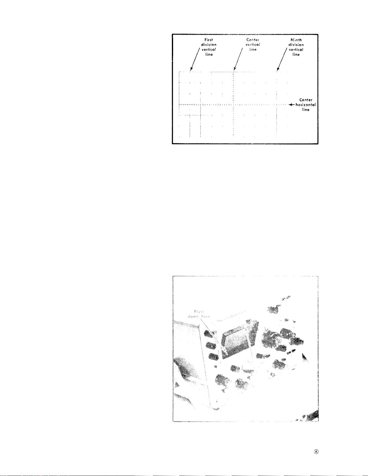
Graticule
Th e g r a t i c u l e o f t h e Ty p e 4 5 3 i s i n t e r n a l l y m a r k e d o n t h e
faceplate of the CRT to p rovid e acc urate, no -para lla x measurements. The graticule is marked with six vertic al and 10
horizontal divisions. Each division is 0.8 centimeter sq uare.
In a d dition, e ac h m a jo r d iv ision is d iv id ed int a five m inor
divisions at the center vertical and horizontal lines. The
vertic al gain and horizonta l timing are calibrated to the
graticule so accurate measurements can be made from the
CRT. The illumination of the graticule lines can be varied
with the SCALE ILLUM control.
Fi g . 2 - 6 sh o w s t h e g r a t i c u l e o f t h e Typ e 4 53 a n d d e f i n e s
the various mea surement lines. The terminology defined here
will be used in all discussions involving graticule measurements.
Fi g . 2 - 6 . D e f i n i t i o n o f m e a s u re m e n t l in e s o n Ty p e 4 5 3 g r a t i c u l e .
re mov e the f ilte r, p ress
down at the bottom of the frame
and pull the top of the filter away from the CRT faceplate
(see Fig. 2-7).
Th e t i n t e d l i g h t f i l t e r m i n i m i z e s l i g h t r e f l e c t i o n s f r o m t h e
face of the CRT to imp ro ve c ontrast when viewing the display under high ambient light conditions. A clear plastic
faceplate protector is a lso p rovided w ith this instrument for
use when neither the me sh nor the tinted filter is used. The
clear faceplate protector provides the best display for waveform p hotographs. It is a lso preferable for view ing high
writing rate displays.
A filter or the facepla te protector should be used at all
times ta protec t the CRT fac eplate from scratc hes. The faceplate protector and the tinted filter mount in the same holder.
Tra c e A l i g n m e n t A d j u st m e n t
If a free-runn ing t ra c e is not p a ra lle l t o the ho rizo nt a l
graticule lines, set the TRACE ROTATION adjustment as fol-
lows. Positio n the tro ce to th e c en te r ho rizonta l line . Ad just
the TRACE ROTATION adjustment (side panel) so the trace
is para llel w ith th e ho rizonta l grat ic ule line s.
Li g ht Fi lte r
Th e m e sh f i l t e r p r o v i d e d w i t h t h e Ty p e 4 5 3 p r o v i d e s s h i e l d ing a gain st ra d iate d EM I (e lectro-mag ne tic int erferen c e) fro m
the face of the CRT. It also serves as a light filter to make
the trace more visible und er ambient light conditions. To
2-10
Fi g . 2 - 7. Re m o v i n g t h e f i lt e r o r f a c e p l a t e p r o t e c t o r .
Page 27

TM 11-6625-1722-15
To r e m o v e t h e l i g h t f i l t e r o r f a c e p l a t e p r o t e c t o r f r o m t h e
holder, press it out to the rear. They can be replaced by
sn a p p i n g t h e m b a c k i n t o t h e h o l d e r.
Tr a c e Find e r
Th e TR A C E FI N D ER p r o v i d e s a m e a n s a f l o c a t i n g a d i s p l a y
which overscans the viewing area either vertically or horizo nta l ly. W he n t h e TRA CE FIND ER b u t to n is p re sse d , t he
display is compressed within the graticule area. T
O locate
and reposition an overscanned display, use the following
procedure.
1. Pre ss the TRA CE FINDER button.
2. While the TRACE FINDER b ut to n is held d epre ssed ,
inc rease the vertic al a nd ho rizo nta l deflec tio n facto rs until
the vertic al deflection is reduced to a bout two divisions and
the horizontal d eflection is reduced to about four d ivisions
(the horizo ntal deflec tion need s to be reduced o nly when in
the external horizontal mode of op eration).
3. Adjust t he v ertic al a nd horizonta l POSITION c ontrols
to c enter the d isp la y ab out the vertical and horizontal c en-
ter lines.
4. Re lea se the TRA CE FINDER button; the displa y sho uld
re main within the view ing area .
Vertical Channel Se lection
Ei t h e r o f t h e i n p u t c h a n n e l s c a n b e u se d f o r si n g l e - t r a c e
displays. Apply the signal to the desired INPUT connector
and set the MODE switch to display the channel used. However, since CH 1 ONLY triggering is provided only in Chan-
nel 1 and the invert feature only in Cha nnel 2, the correct
channel must be selected to take advantage of these features. For d ual-trace displays, c onnect the signals to both
INPUT c onn ec t ors a nd se t t he M ODE switc h to o ne o f the
dual-trace positions.
Vertical Ga in Adjustment
To c h e c k t h e g a i n o f e i t h e r c h a n n e l , s e t t h e V O L TS/ D I V
sw i t c h t o 2 0 m V . Se t t h e C A L IBRA TO R sw i t c h t o . 1 V a n d
connect the 1 kHz CAL connector to the INPUT of the chan-
nel used . The vertica l deflec tion should be exac tly five
divisions.
If not, a d just t he f ront -p ane l G AIN a d just m ent
for exac tly five divisions of d eflec tion.
NOTE
If t he g a in o f the t wo c ha nne ls m ust b e c lo se ly
matched (such as for ADD mode operation), the
ADJUSTMENT p roc edure given in the Calibration
se c t i o n sh o u ld b e u se d .
Th e b e s t m e a s u r e m e n t a c c u r a c y w h e n u s i n g p r o b e s i s p r o vided if the GAIN adjustment is made with the p robes inst a l l e d ( se t t h e C A LIB RA TO R sw i t c h t o 1 V ) . A l so , t o p r o v id e
the most accurate measurements, ca librate the vertical g ain
of the Type 453 at the temperature at which the measurement
is to be ma de.
Ste p A tt e nua t o r Ba l a nc e
To c h e c k t h e s t e p a t t e n u a t o r b a l a n c e o f e i t h e r c h a n n e l ,
se t t h e In p u t C o u p l i n g sw i t c h t o G N D a n d se t t h e A SW EEP
MODE swic h to AUTO TRIG to provide a free-running trace.
Change the VOLTS/DIV switc h from 20 mV to 5 mV. If the
trac e moves vertically, adjust the front-panel STEP ATTEN
BA L a d j u st m e n t a s f o ll o w s ( a llo w a t l e a st 1 0 m i nut e s w a rm
up b efore performing this a djustment].
1. With th e Inp ut Coupling switch se t to GND a nd the
VOLTS/ DIV sw itc h set to 20 mV, m ove the tra ce to the center
horizontal line of the graticule with the vertica l POSITION
control.
2. Se t the VOLTS/ DIV switc h to 5 m V a nd a djust t he
STEP A TTEN B A L a d j u st m e n t t o r e t u r n t h e t r a c e t o t h e c e n t e r
horizonal line.
3. Re c he ck step a ttenuator bala nc e and rep eat adjustm ent
until no trac e shift oc curs a s the VOLTS/ DIV switc h is cha nged from 20 mV to 5 mV.
Sig na l C o nn e c ti o ns
In gen era l, p rob es o ff er th e m o st c on ve nient me a ns o f c o nnec ting a signal to the input of the Type 453. The Tektronix
probes are shielded to prevent pickup of electrostatic interferenc e. A 10X a ttenuator probe offe rs a high input imped ance and allows the circuit under test to perform very close
to normal operating c onditions. However, a 10X p robe
also attenuates the input signal 10 times.
Th e Te k t r o n i x
P60 45 Fie ld Ef fe c t Tra n sisto r p ro b e a n d a c c e ssory p o w er
su p p l y o f f e r t h e sa m e h i g h - i n p u t i m p e d a n c e a s t h e 1 0 X
probes. However, it is particularly useful since it provides
wide-band operatian while presenting no attenuation (1X
gain) and a low input capacitance. To obtain maximum
bandwidth when using the probes, observe the grounding
considerations given in the probe manual. The probe-toconnector adapters and the bayonet-ground tip provide the
best frequency response. Remember that a ground strap
only a few inches in length can produc e several percent of
ringing wh en opera ting at th e hig he r fre q ue nc y lim it o f this
sy st e m . Se e y o u r Te kt r o n i x, I n c . c a t a l o g f o r c h a r a c t e ri st i c s
and compatibility of probes for use with this system.
In hig h-freque nc y a p p lic a tions re q uiring ma ximu m ove ra ll
bandwidth, use coaxial cables terminated at both ends in
their characteristic impedanc e. See the discussion on coa xia l cab les in th is sec tio n fo r more info rma tio n.
Hig h-lev el, lo w-fre que nc y sig na ls c a n b e c onnec ted directly
to the Type 453 INPUT connectors with short unshield ed
leads. Th is c ou p ling m et ho d w orks b est fo r sig na ls b elow
about one kilohertz and deflection foctors above one volt/
division. When this method is used, establish a common
ground between the Type 453 and the equipment under test.
Attempt to position the leads away from any source of interferenc e to avoid errors in the display. If interference is
excessive with unshielded leads, use a coaxial cable or a
probe.
Lo a d in g Ef fe c t o f t he Ty p e 4 5 3
As nearly as possible, simulate actual operating c onditions in the equipment under test. Otherwise, the equipment
under test may not produce a normal signa l. The 10X
attenuator probe and field effect transistor probe mentioned
previously offer the least circuit loading. See the probe
instru c tio n man ua l fo r load ing cha ra c te ristics o f t he ind ividual probes.
2-11
Page 28

TM 11-6625-1722-15
When the sig nal is c oupled directly to the input of the
Ty p e 4 5 3 , t h e i n p u t i m p e d a n c e i s a b o u t o n e m e g o h m
paralleled by about 20 pF. When the signal is coupled to
the input through a c oaxia l c ab le, the effeclive input capacitance depends upon the type and Iength of cable used.
Se e t h e f o l l o w i n g d i s c u ss i o n f o r
inf orrna tio n o n obt a ining
maximum frequency responspe with coaxial cables.
Th e s i g n a l c a b l e s u s e d t o c o n n e c t t h e s i g n a l 1 0 t h e t y p e
453 INPUT conn ec tors ha ve a Ia rg e effec t on t he ac curac y
of the displayed high-frequency waveform.
To m a i t a i n t h e
high-frequenc y characteristics of the app lied signal, highquality low-loss coaxial cable should be used. The cable
sh o u l d b e t e r m i n a t e d a t t h e Ty p e 4 5 3 IN PU T c o n n e c t o r in i t s
characteristic impedonce.
with differing characteristic impedances,
If it is n ec e ssary t o u se c a b les
use suitab le imped-
ance-matching devices to provide the correct transition, with
minimum loss, from one impedance to the other.
Th e c h a r a c t e r i s t i c i m p e d a n c e , v e l o c i t y o f p r o p a g a t i o n a n d
nature of signa l lOSSeS in a c oa xial c ab le a re det ermined
by the physical and electrical characteristics of the cable.
Lo sse s c a u se d b y e n e rg y d i ssip a t i o n in t h e d i e le c t ric a re
proportional to the signal frequency. Therefore, much of
the high-frequency information in a fast-rise p ulse can be
lost in o nly a few fee t of intercon ne c tin g c able if it is no t
the c orrec t type. To be sure of the high-frequency resp onse
of the system when using cables longer than about five feet,
observe the transient response of the Type 453 and the
int ercon ne c tin g c ab le with a fast-rise
pulse generator (gen-
erator risetime Iess than 0.5 nanoseconds).
DC c om po nents. The pre -charging ne twork inco rpora te d
in this u nit a II
OWS the inp ut-c oupling cap ac itor to charge to
the DC source voltage level when the Inp ut Coupling switc h
is se t to G ND. Th e p ro c ed ure f or using this fe ature is a s
follows:
1. Be fore c onn ec ting the signa l c ontaining a DC c om ponent to the Typ e 453 INPUT connector, set the Input Coupling
sw i tc h t o G N D. Th e n c o n n e c t t h e si g n a l t o t h e IN PUT
connector.
2. Wa it a bout one se c ond for the coupling c apa citor to
charge.
3. Se t the In put C ouplin g switc h to A C. Th e t rac e (display) will remain on the screen and the AC component of
the signal c an be measured in the normal ma nner.
Deflection Fa c tor
Th e a m o u n t o f v e r t i c a l d e f l e c t i o n p r o d u c e d b y a si g n a l
is d eterm ined by the sig na l a m plitude , th e attenua tio n fac to r
of the probe (if used), the setting of the VOLTS/DIV switch
and the setting of the VARIABLE VOLTS/DIV control. The
calibrated deflection factors indicated by the VOLTS/DIV
sw i t c h e s a p p l y o n l y w h e n t h e V A RI A BLE c o n t r o l i s se t t o
the CAL position.
Th e V A R I A B L E V O L TS/ D I V c o n t r o l p r o v i d e s v a r i a b l e
(unc alibrated) vertical deflection between the c alibrated
se t t i n g s o f t h e V O LTS/ D IV sw i t c h . Th e V A RIA BLE c o n t r o l
extends the maximum vertical deflec tion factor of the Type
453 to a t lea st 25 volts/ divisio n (10 volts po sition).
Input Coupling
Th e C h a n n e l 1 a n d 2 l n p u t C o u p l i n g sw i t c h e s a l l o w a
choice of input caupling. The type of display desired will
determine the coupling used.
Th e D C p o s i t i o n c a n b e u s e d f o r m o st a p p l i c a t i o n s . H o w ever, if the DC component of the signal is much larger than
the AC component, the AC p osition vvill probab ly provide a
better display. DC coupling should be used to display AC
si g n a l s b e l o w a b o u t 1 6 h e l t z a s t h e y w i l l b e a t t e n u a t e d i n
the AC position.
In t he A C p o sitio n, t he D C c o mpone nt o f t he sig nal is
blocked by a capacitor in the input circuit. The low-frequency response in the AC position is about 1.6 hertz (–3 dB
point). Therefore,
so m e l o w - f re q u e n c y d i st o rt i o n c a n b e
expected near this frequency limit. Distortion will also
appear
in sq ua re w aves w hic h hav e low-f req ue nc y c om-
ponents.
Th e G N D p o s i t i o n p r o v i d e s a g r o u n d r e f e r e n c e a t t h e
inp ut of the Typ e 453. The sig na l app lied to the inp ut con-
nec tor is internally disc onnec ted but not grounded. The
inp ut c irc uit is he ld at g rou nd p ote nt ial, e limina tin g th e ne ed
to externally ground the input to establish a DC ground
re fe renc e.
Th e G N D p o s i t i o n c a n a l s o b e u se d t o p r e - c h a r g e t h e
coupling capacitor to the average voltage level of the signal
applied to the INPUT connector. This allows measurement
of only the AC component of signals having both AC and
Dua l-Tra ce O pe ration
Alte rnate Mode. Th e A L T p o s i t i o n o f t h e M O D E s w i t c h
produces a disploy which alternates between Channel 1 and
2 w ith eac h swe ep of t he CRT. A ltho ug h the ALT mod e
can be used at all sweep rates, the CHOP mode provides
a more satisfactory display at sweep rates below about 50
microseconds/division. At these slower sweep rates, alternate
mode switching becomes visually perceptible.
Pro p e r in t erna l trig g e rin g in t h e A LT m o d e c a n b e o b -
tained in either the NORM or CH 1 ONLY positions of the
TRI G G E R s w i t c h . W h e n i n t h e N O R M p o si t i o n , t h e s w e e p i s
triggered from the signal on each channel. This provid es a
st a b l e d i sp l a y o f t w o u n re l a t e d sig n a l s, b u t d o e s n o t in d i c a t e
the time relationship between the signals. In the CH 1 ONLY
position, the two signals are displayed showing true time
re la tio nship . If the sig na ls a re n ot tim e relate d , th e Ch a nn el
2 wa ve fo rm will b e unsta ble in the CH 1 ONLY po sition.
Chopped Mode. Th e C H O P p o si t i o n o f t h e M O D E sw i t c h
produces a display which is electronically switched between
channels. In general, the CHOP mode provides the best
display at sweep rates slower than about 50 microseconds/
division, or whenever dual-trace, single-shot phenomena are
to b e displayed. At faster sweep rates the chopped sw itc hing bec ome s ap pare nt and m ay inte rfere with th e disp la y.
Pro p e r in tern al t rig g e rin g fo r t h e CHO P mo d e is p ro vid e d
with the TRIGGER switch set to CH 1 ONLY. If the NORM
position is used, the sweep circuits are triggered from the
between-channel switching signal and both waveforms will
2-12
Page 29

TM 11-6625-1722-15
be unstable. External triggering provides the same result as
CH 1 ONLY triggering.
Tw o s i g n a l s w h i c h a r e t i m e - r e l a t e d c a n b e d i s p l a y e d i n
the chop ped mode showing true time relationship. If the
si g n a l s a r e n o t t i m e - r e la t e d , t h e C h a n n e l 2 d i sp l a y w i ll
appear unstable. Two single-shot, transient, or random
si g n a l s w h i c h o c c u r w i t h in t h e t i m e i n t e rv a l d e t e rm i n e d b y
the TIME/ DIV switch (10 times sweep rate) c an be compared
using the CHOP mod e. To correctly trigger the sweep for
maximum resolution, the Channel 1 signal must precede the
Channel 2 signal. Since the signals show true time relation-
sh i p , t i m e - d i f f e re n c e m e a su r e m e n t s c a n b e m a d e .
Channel 1 Output and Cascaded Operation
If a lower def lec tio n fa c to r tha n provid e d b y t he VO LTS/
DIV switc hes is d esired, Cha nne l 1 c an b e use d a s a w ide band preamplifier for Channel 2. Apply the input signal to
the Channel 1 INPUT connector. Connect a 50-ohm BNC
cable (18-inch or shorter cable for maximum cascaded fre-
quency response) between the CH 1 OUT (side panel) and
the Channel 2 INPUT c onnec tors. Set the MODE switch to
CH 2 and the TRIGGER switch to NORM. With both VOLTS/
DIV switches se t to 5 mV, the d eflection factor will be less
than one millivolt/division.
To p r o v i d e c a l i b r a t e d o n e m i l l i v o l t / d i v i s i o n d e f l e c t i o n
factor, c onnect the .1 volt Calibrator signa l to the Channel 1
INPUT c o nn ec t or. Set t he C H 1 VOLTS/ D IV sw itc h t o . 1
and the CH 2 VOLTS/DIV switch to 5 mV. Adjust the Channel 2 VARIABLE VOLTS/ DIV control to produc e a disp la y
exactly five divisions in amplitude. The casc aded deflection
factor is determined by dividing the C H 1 VOLTS/ DIV switc h
se t t i n g b y 5 ( C H 2 V O LTS/ D IV sw i t c h a n d V A RIA BLE c o n t r o l
re main a s set a bov e). For exa mple, with th e CH 1 VO LTS/
DIV sw itch se t to 5 mV the calibrated de flec tion fac tor will
be 1 millivolt/division; CH 1 VOLTS/DIV switch set to 10 mV,
2 millivolts/ divisio n, e tc .
Th e f o l l o w i n g o p e r a t i n g c o n si d e r a t i o n s a n d b a s i c a p p l i -
cations may suggest other uses for this feature.
1. If A C c oupling is d esired , set the C ha nn el 1 Inp ut
Coupling switch to AC and leave the Channel 2 Input
Coupling switc h set to DC. When both Input Coupling
sw i t c h e s a r e se t t o D C , D C si g n a l c o u p l in g i s p r o v id e d .
2. Kee p b oth v ertic al POSITION c ontro ls set nea r m id-
ra ng e.
one of the POSITION controls being turned away from
midrange, correct operation can be obtained by keeping
the Cha nnel 2 POSITION control near midrange and using
the Channel 1 POSITION control to position the trac e near
the desired locatian. Then, use the Channel 2 POSITION
control far exact positioning. This method will keep both
Input Pre amps o perating in t he ir line a r ra nge.
least 25 millivo lts/ division of CRT d isp lay in all CH 1 VOLTS/
DIV switc h positions.
DIV contro l have no effect on the signal availab le at the
CH 1 OUT connector.
ance matching stage with or without voltage gain. The
If th e in put sig n a l ha s a DC le ve l w hic h n ec essit ate s
3. The outp ut vo lta ge a t the C H 1 OUT c on nectar is a t
4. The MODE switch a nd Cha nne l 1 VA RIABLE VOLTS/
5. The C ha nn el 1 Input Pream p c a n b e used as an impe d -
inp ut re sista nc e is on e me g ohm a nd the o utp ut re sista nc e is
about 50 ohms.
6. The dynamic ra ng e of the Ch anne l 1 Inp ut Pre amp is
equal to about 20 times the CH 1 VOLTS/DIV setting. The
CH 1 OUT signal is nominally at 0 volt DC for a 0 volt DC
inp ut le ve l [Ch annel 1 POSITIO N c ontro l c ente red ). Th e
Chanel 1 POSITION control can be used to center the output signal within the dynamic range of the amplifier.
7. If dua l-trace ope ration is used , the signal a pplie d to
the Channel 1 INPUT connector is disp la yed when Channel
1 is turned on. When Channel 2 is turned on , the amp lified
si g n a l i s d i sp l a y e d . Th u s, C h a n n e l 1 t r a c e c a n b e u se d t o
monitor the input signal while the amplified signal is dis-
played by Channel 2.
8. In spec ial a pplic a tions w he re the fla t fre quency re -
sp o n se o f t h e Ty p e 4 5 3 i s n o t d e si re d , a f il t e r i n se r t e d
between the CH 1 OUT and Channel 2 INPUT connector
allows the oscilloscope to essentially take on the frequency
re sp onse of the filte r. C om bine d w ith met ho d 7, the inp ut c an
be monitored by Channel 1 and the filtered signal displayed
by Channel 2.
9. By using Channe l 1 a s a 5X lo w-le ve l v oltag e p reamplifier (5 mV position), the Channel 1 signal available
at the CH 1 OUT connector can be used for any application
where a low-impedance preamplifier signal is needed.
Re m e m b e r t h a t i f a 5 0- o h m lo a d i m p e d a n c e i s u se d , t h e
si g n a l a m p l i t u d e w i ll b e a b o u t o n e - h a l f.
Algebraic Addition
General. Th e A D D p o si t i o n o f t h e M O D E s w i t c h c a n b e
used to d isplay the sum or d ifferenc e of two signals, for
common-mode rejection to remove an undesired signal or for
DC offset (ap plying a DC voltage to one channel to offse t
the DC component of a signal on the other c hannel).
Th e c o m m o n - m o d e r e j e c t i o n r a t i o o f t h e Ty p e 4 5 3 i s
greater than 20:1 at 20 megahertz for signal amplitudes up
to eight times the VOLTS/ DIV switch setting. Rejec tion ratios
of 100:1 can typically be achieved between DC and 5 megahertz b y ca reful a djustm ent of the gain of either c hannel
while observing the displayed common-mode signal.
Deflection Fac tor. Th e o v e r a l l d e f l e c t i o n i n t h e A D D
position of the MODE switch when both VOLTS/DIV switches
are set to the same position is the same as the deflection
factor indicate d by eithe r VOLTS/ DIV sw itch. The a mplitude of an added mod e display can be determined directly
from the resulta nt CRT deflection multiplied by the deflec tion factor indicated by either VOLTS/DIV switch. However, if the CH 1 and CH 2 VOLTS/ DIV switches are set to
different deflection factors, resultant voltage is difficult to
determine from the CRT display. In this case, the voltage
amplitude of the resultant display can be determined accura tely only if th e amp litud e o f the sig na l a p p lied to eit he r
channel is known.
Pre c a u tion s.
be observed when using the ADD mode.
1. Do no t exceed the inp ut voltag e
453.
Th e f o l l o w i n g g e n e r a l
precautions should
ra ting o f the Type
2-13
Page 30

TM 11-6625-1722-15
2. Do n ot a pply sig na ls th at e xcee d on e quiva lent o f
about 20 times the VOLTS/DIV switch setting. For example,
with a VOLTS/DIV switch setting of .5, the voltage applied
to that channel should not exceed a bout 10 volts. Larger
voltages may disto rt the disp la y.
3. Use ve rtic al POSITION c ontro l se ttin gs w hic h m ost
nearly position the signa l of ea ch cha nnel to mid-sc reen
when viewed in either the CH 1 or CH 2 positions of the
MODE switch. This insures the greatest dynamic range for
ADD mode opera tion.
4. For similiar re sp onse from ea c h c ha nnel, set both Input
Coupling switches to the same position.
Trig g e r So u r c e
INT. Fo r m o st a p p l ic a t i o n s, t h e sw e e p c a n b e t ri g g e r e d
int erna lly. In th e INT p o sit ion o f t he Trig g ering SO URC E
sw i t c h , t h e t r ig g e r si g n a l i s o b t a i n e d f r o m t h e V e r t i c a l
Defle ction System. The TRIGGER sw itch pro vide s furthe r
se l e c t i o n o f t h e i n t e r n a l t ri g g e r si g n a l ; o b t a i n e d f r o m t h e
Channel 1 signal in the CH 1 ONLY position, or from the
displayed signal when in the NORM position. For singletrac e displays of either channel, the NORM position provides the most co nvenient operation. However, for dualtrac e displays special c onsiderations must be made to provide
the c orrec t display. Set Dual-Trace Op eration in this sec tion
for dual-tra ce trig gering information.
LI N E. Th e L I N E p o s i t i o n o f t h e SO U RC E s w i t c h c o n n e c t s
a sample of the power-line frequency to the Trigger Gen-
erator circuit. Line triggering is useful when the input signal
is time -re late d t o t he lin e f req ue nc y. It is a lso u se fu l f or
providing a stable display of a line-frequency component
in a c om plex wa ve fo rm .
EX T. An externa l signal conected to the EXT TRIG INPUT
connector can be used to trigger the sweep in the EXT
position of the Triggering SOURCE switch. The external signal must b e time-related to the disp la yed signal for a stable
display. An external trigger signal can be used to provide
a triggered display when the internal signal is too low in
amplitude for correct triggering, or contains signal comp onents on wh ich it is not de sired to trigge r. It is also useful
when signal tracing in amplifiers, phase-shift networks, wavesh a p i n g c i rc u i t s, e t c . Th e si g n a l f r o m a sin g l e p o i n t i n t h e
circuit under test can be connected to the EXT TRIG INPUT
connector through a signal probe or cable. The sweep is
then trigg ered by the sa me signal at a ll times a nd allows
amplitude, time relationship or waveshape changes of
si g n a l s a t v a ri o u s p o i n t s i n t h e c i rc u i t t o b e e x a m i n e d w i t h out resetting the trigger controls.
frequency components of the trigger signa l which can trig ger
the sweep.
AC. Th e A C p o si t i o n b l o c k s t h e D C c o m p o n e n t o f t h e
trigger signal. Signals with low-frequency components below
about 30 hertz are attenuated. In general, AC coupling can
be used for most applications. However, if the trigger signal
contains unwanted components or if the sweep is to be
triggered at a low repetition rate or a DC level, one of the
re maining COUPLING sw itc h p osition s w ill p rovid e a bet ter
display.
Th e t r i g g e r i n g p o i n t i n t h e A C p o s i t i o n d e p e n d s o n t h e
average voltage level of the trigger signal. If the trigger
si g n a l s o c c u r in a ra n d o m f a sh i o n , t h e a v e r a g e v o l t a g e l e v e l
will vary, causing the triggering point to vary also. This shift
of the triggering point may be enough so it is impossible to
maintain a stable display. In such cases, use DC coupling.
LF REJ . In th e LF REJ p o sitio n, DC is re je c te d a nd sig na ls
below about 30 kilohertz are attenuated. Therefore, the
sw e e p w i ll b e t r ig g e re d o n l y b y t h e h i g h e r - f re q u e n c y c o m -
ponents of the signal. This position is particularly useful
for providing sta ble triggering if the trigger signal contains
line -frequenc y com po ne nt s. Also , in the ALT positio n of the
MODE switch, the LF REJ position provides the best display
at high sweep rates when comparing two unrelated signals
(TRIGGER switc h set to NORM).
HF REJ. Th e H F R EJ p o s i t i o n p a s se s a l l l o w - f r e q u e n c y
sig na ls b et we en a bout 30 hertz a nd 50 kilo hertz. DC is
re jecte d a nd sig na ls o utsid e the g ive n ra ng e are a tt enuate d .
When trigg ering from co mplex w avefo rms, this p ositio n is
useful for providing sta ble d isp lay of low-frequenc y components.
DC. DC c oupling ca n b e used to pro vide sta ble trigg ering
with low-frequency signals which would be attenuated in
the AC position, or with low-repetition rate signals. The
LEVEL c o n t ro l c a n b e a d j ust e d t o p r o vi d e t r ig g e r in g a t t h e
desired DC level on the waveform. When using internal
triggering, the setting of the Channel 1 and 2 POSITION
controls affects the DC trigger level.
DC trigg er coup ling should not b e used in the ALT dua ltrac e mod e if the TRIGGER switch is set to NORM. If used ,
the sweep will trigger on the DC level of one tra ce a nd then
either lock out completely or free run on the other trace.
Correct DC triggering for this mode c an be obtained with
the TRIGGER switch set to CH 1 ONLY.
Trig g e r Slo p e
sa m e a s d e sc r ib e d f o r EX T e x c e p t t h a t t h e e x t e rn a l t r ig g e r in g
si g n a l i s a t t e n u a t e d 1 0 t i m e s. A t t e n u a t i o n o f h i g h - a m p l it u d e
external triggering signals is desirable to broaden the range
of the Triggering LEVEL control.
sw i t c h i s se t t o L F REJ, a t t e n u a t i o n is a b o u t 2 0 :1 .
Tr ig g e r C o u p l i n g
Fo u r m e t h o d s o f c o u p l in g t h e
circuits can be selected with
sw i t c h e s. Ea c h p o si t i o n p e rm i t s
2-14
When the COUPLING
trigger signal to the trigger
the Trig gering COUPLING
se l e c t i o n o r re j e c t io n o f t h e
Th e t r i g g e r i n g SL O P E s w i t c h d e t e r m i n e s w h e t h e r t h e t r i g g e r
circuit responds on the positive-going or negative-going
portion of the trigger signal. When the SLOPE switch is in
the + (positive-going) p osition, the display sta rts with the
positive-going portion of the waveform; in the - (negativegoing) position, the display starts with the negative-going
portion of the waveform (see Fig. 2-8]. When several cycles
of a signal appear in the display, the setting of the SLOPE
sw i t c h is o f t e n u n i m p o r t a n t . Ho w e v e r , if o n l y a c e rt a i n
portion of a cycle is to be displayed, correct setting of the
SLO P E s w i t c h i s i m p o r t a n t t o p r o v i d e a d i s p l a y w h i c h st a r t s
on the desired slope of the input signal.
Page 31

TM 11-6625-1722-15
Fig. 2 -8 . Effec ts of Triggering LEVEL c ontrol a nd SLOPE sw itch.
2-15
Page 32

TM 11-6625-1722-15
Trig g e r Le v e l
Th e Tr i g g e r i n g L E V E L c o n t r o l d e t e r m i n e s t h e v o l t a g e l e v e l
on the trigger signal at which the sweep is triggered. When
the LEVEL control is set in the + region, the trigger circ uit
re sp ond s a t a m ore p osit ive p oint o n t he t rig g er sig na l.
When the LEVEL co ntrol is set in the - reg ion, the trigg er
circuit responds at a more negative point on the trigger
si g n a l . Fi g . 2 - 8 i ll u st ra t e s t h i s e f f e c t w i t h d i ff e re n t se t t i n g s
of the SLOPE switc h.
se t t h e LEV EL c o n t ro l , f ir st se l e c t t h e Tri g g e r in g
To
SO U RC E , C O U PL I N G a n d SL O P E. Th e n s e t t h e L EV EL
control fully counterclockwise ond rotate it clockwise until
the display starts at the desired point.
High-Freque nc y Stability
Th e H F STA B c o n t r o l ( A o n l y ) i s u se d t o p r o v i d e a s t a b l e
display of high-frequency signals. If a stable display cannot
be obtained using the A LEVEL control (trigger signal must
have adequate amp litude), adjust the HF STAB control for
minimum horizontal jitter in the display. This control has
litt le e ffec t w ith lo w-freq ue nc y sign a ls.
A Swe ep Triggered Light
Th e A SW E EP TR I G ’ D I i g h t p r o v i d e s a c o n v e n i e n t i n d i c a tion of the condition of the A Triggering c ircuit. If the A
Tr i g g e r i n g c o n t r o l s a r e c o r r e c t l y a d j u s t e d w i t h a n a d e q u a t e
trigger signal app lied, the light is on. However, if the A
LEVEL c o ntr o l is m isa d ju st ed , t he A C O UPLIN G o r A
SO U RC E s w i t c h e s i n c o r r e c t l y se t o r t h e t r i g g e r si g n a l t o o
low in o mplit ud e, t he A SWEEP TRIG’ D lig ht w ill b e off.
Th i s f e a t u r e c a n b e u s e d a s a g e n e r a l i n d i c a t i o n o f c o r r e c t
triggering. It is particularly useful when setting up the
trigger circuits when a trigger signal is availab le without a
trac e disp layed on the CRT and it a l
So indicates that the A
sw e e p i s c o r re c t l y t ri g g e r e d w h e n o p e r a t i n g i n t h e D ELA Y ED
SW E EP ( B ) m o d e .
si g n a l s w i t h re p e t i t io n r a t e s b e l o w a b o u t 2 0 h e r t z. Th i s m o d e
provides an indication of an adequate trigger signal as well
as the correctness of trigger control settings, since there is
no d isp lay w ithout proper trig gering. Also, the A SWEEP
TRI G ’ D l i g h t i s o f f w h e n t h e A sw e e p i s n o t c o r r e c t l y
triggered.
SI N G LE SW EEP. When the sig nal to be disp layed is no t
re pet itive o r va ries in amplitude, sh a p e or tim e, a con ve ntional repetitive display may produc e an unsta ble presentation. To avoid this, use the single-sweep feature of the Type
453. The SINGLE SWEEP mo d e c an also be use d to p ho tograph a non-repetitive signal.
To u s e t h e SI N G L E SW E EP m o d e , f i r s t m a k e su r e t h e
trigger c ircuit will respond to the event to b e displayed .
Se t t h e A SW E EP M O D E s w i t c h t o A U TO TR I G o r N O R M
TRI G a n d o b t a i n t h e b e s t p o s si b l e d i s p l a y i n t h e n o r m a l
manner (for random signals set the trigger circuit to trigger
on a signal which is approximately the same omplitude and
frequency a s the rand om signa l). Then, set the A SWEEP
MODE switch to SINGLE SWEEP and press the RESET button.
When the RESET b utt on is p ushe d, t he ne xt trigg er p ulse
init ia te s th e sw eep an d a single t ra c e w ill be pre se nt ed on
the sc reen. After this sw eep is complete, the A Sw eep Generator is
"lo c ke d o ut " u nt il re se t. Th e RESET light lo cate d
insid e t he RESET butto n lights whe n the A Sw ee p Ge nerato r
circuit has been reset and is ready to produce a sweep;
it g oes o ut a fter t he sw eep is c om ple te . To p repa re the
circuit for another single-sweep display, press the RESET
button again.
Se le c ti ng Sw e e p Ra t e
Th e A A N D B TI M E / D I V s w i t c h e s s e l e c t c a l i b r a t e d s w e e p
ra tes fo r th e Sw ee p Gen erato rs.
Th e A a n d B V A R I A B L E
controls provide continuously variable sweep rates between
the settings of the TIME/ DIV switches. Whenever the UNCAL
A OR B light is on, the sweep rate of either A or B Sweep
Generator, or both, is uncalibrated. The light is off when
the A VARIABLE (front pa nel) and B TIME/DIV VARIABLE
(side panel) controls are both set to the CAL position.
A Sweep Mode
AUTO TRIG. Th e A U TO TRI G p o s i t i o n o f t h e A SW E EP
MODE switch provid es a stable display when the A LEVEL
control is correctly set (see Trigger Level in this section] and
a trigger signal is available. The A SWEEP TRIG’D light
ind ic ate s wh en th e A Sw eep G en era to r is trig gere d .
When the trigg er rep etition rat e is less then a bout 20
hertz, or in the absenc e of an adeq uate trigger signal, the
A Sweep Generator free runs to produce a referenc e trace.
When a n a dequate trigger sig na l is a ga in a pp lied , the
free-running condition ends and the A Sweep Generator is
triggered to produce a sta ble display (with correct A LEVEL
control setting.)
NORM TRIG . Operation in the NORM TRIG position
when a trigger signal is applied is the same as in the AUTO
TRI G p o s i t i o n . H o w e v e r , w h e n a t r i g g e r s i g n a l i s n o t p r e s e n t ,
the A Sweep Generator rem ains off a nd there is no disp la y.
Th e A SW EF P TR I G ’ D l i g h t i n d i c a t e s w h e n t h e A s w e e p i s
triggered. The NORM TRIG mode c an be used to display
2-16
Th e sw e e p r a t e o f t h e A Sw e e p G e n e r a t o r i s b r a c k e t e d
by the two black lines on the clear plastic flange of the
TI M E/ D I V s w i t c h ( s e e F i g . 2 - 9 ) . Th e B Sw e e p G e n e r a t o r
sw e e p ra t e i s i n d i c a t e d b y t h e d o t o n t h e D ELA Y ED SW EEP
kno b. When th e dot on the out er knob is se t to the sa me
position as the lines on the inner knob, the two knobs lock
together and the sweep ra te of b oth Sw eep Generators is
changed at the same time.
Ho weve r, w he n t he DELA YED
SW E EP k n o b i s p u l l e d o u t w a r d , t h e c l e a r p l a st i c f l a n g e i s
disengaged and only the B Sweep Generator sweep rate is
changed. This allows changing the delayed sweep rate
wihout changing the delay time determined by the A Sweep
Generator.
When ma king time m ea surements from the g ratic ule, the
area between the first-division and ninth-division vertical lines
provides the most linear time measurement (see Fig. 2-10).
Th e r e f o r e , t h e f i r s t a n d l a st d i v i s i o n o f t h e d i s p l a y s h o u l d n o t
b e used for making ac curat e time me asure me nts. Po sitio n
the start of the timing area to the first-division vertical line
and set the TIME/DIV switch so the end of the timing area
falls b etw een the first- a nd ninth-division vertica l lines.
Page 33

Fig. 2-9.
TM 11-6625-1722-35
Sw e e p M a g n i f i c a t i o n
Th e s w e e p m a g n i f i e r e x p a n d s t h e s w e e p t e n t i m e s. Th e
center division of the unmagnified display is the portion
visible on the sc reen in mognified form (see Fig. 2-11]. Equivalent length of the magnified sweep is about 100 divisions;
any 10 division portion may be viewed by adjusting the
horizontal POSITION c ontrol to b ring the d esired p ortion
onto the viewing area. The FINE position control is particula rly useful w he n th e magn ifie r is on, as it prov id es p osition-
ing in sm all in c reme nt s fo r more prec ise c ontro l.
To u s e t h e m a g n i f i e d s w e e p , f i r s t m o v e t h e p o r t i o n o f t h e
display which is to be expanded to the center of the graticule. Then set the MAG switch to X10. The FINE position
control can be adjusted to position the magnified display
Fig . 2 - 11 . O p e ra t i o n o f sw e e p m a g n if ie r .
as desired. The light located below the MAG switch is on
whenever the magnifier is on.
When the MA G switc h is set to X10, the sw ee p ra te is
determined by dividing the TIME/DIV switch setting by 10.
Fo r e x a m p l e , i f t h e TIM E/ D IV sw i t c h i s se t t o
magnified sweep rate is 0.05 microsecond/division. The
magnified sweep rate must be used for all time measurements when the MAG switch is set to X10. The magnified
sw e e p r a t e i s c a l ib ra t e d w h e n t h e UN C A L A O R B l ig h t
is o ff.
Delayed Sweep (B)
Th e d e l a y e d s w e e p ( B s w e e p ) i s o p e r a b l e i n t h e A I N TE N
DURING B and DELAYED SWEEP (B) positions of the HORIZ
DISPLAY sw itch. The A sw eep rate a long with the DELAY-
TI M E M U L TI P L I E R d i a l s e t t i n g d e t e r m i n e s t h e t i m e t h a t t h e
B sw e e p i s d e la ye d . Sw e e p ra t e o f t h e d e la ye d p o rt i o n i s
determined by the B TIME/DIV (DELAYED SWEEP) switch
se t t i n g .
In t he A IN TEN DURIN G B p ositio n, t he d ispla y w ill
appear similar to Fig. 2-12A. The amount of delay time
between the start of A sweep and the intensified portion is
determined by the setting of the A TIME/DIV switch and the
DELAY-TIME MULTIPLIER d ial.
Fig . 2 -1 0. A r e a o f g ra t i c u le u se d f or a c c u ra te t i m e m e a su re m e n t s.
Fo r e x a m p l e , t h e d e l a y i n d i c a t e d b y t h e D ELA Y - TI M E
MULTIPLIER dial setting shown in Fig. 2-13 is 3.55; this cor-
re sp ond s t o 3.55 C RT d ivisio ns of A sw eep . Th is reading
multiplied by the setting of the A TIME/DIV switch gives
the calibrated delay time before the start of the B sweep
(see B Sweep Mo de whic h follows). The intensified po rtion
of the display is produced by the B sweep. The length of
2-17
Page 34

TM 11-6625-1722-15
B SW EEP M O D E. Th e B SW EE P M O D E s w i t c h p r o v i d e s
two mod es of delayed sweep operation. Fig. 2-14 illustrates
the difference b etween these t
Wo modes. In the B STARTS
AFTER DELAY TIME p osition, the B sweep is presented immediately after the delay time (see Fig. 2-14A]. The B sweep
is trig gere d at a se lected point on A sw ee p to pro vid e the
delay time (B sweep essentially free running]. Since the delay
time is the sa me for each sweep,
the d isp la y appears sta ble
In the TRIG GERABLE AFTER DELAY TIM E p o sition , t he B
sw e e p o p e r a t e s o n l y w h e n i t is t ri g g e r e d ( b y Tri g g e r C i rc u i t s)
after the selected delay time (see Fig. 2-14B). The B Triggring controls operate as described in this section.
Delayed Swe ep Op era tion. To o b t a i n a d e l a y e d s w e e p
display use the following procedure.
1. Obt ain a sta ble d isp lay w ith the HORIZ DISPLAY
sw i t c h se t t o A .
2. Se t the HORIZ DISPLAY switch to A INTEN DURING
B.
3. Se t the B SWEEP M ODE switc h to the d esired se tt ing.
If TRIG GERABLE AFTER D ELA Y TIM E is se lec te d , c o rrec t B
Tr i g g e r i n g i s a l s o n e c e s sa r y ,
4. Set the d ela y time w ith th e A TIME/ DIV switch a nd
the DELAY-TIME MULTIPLIER dial.
Fig . 2 -1 2. ( A ) A I NTEN D URIN G B d i sp la y ( DELAY -TIM E M ULTIPLIER, 2 .95 ; A TIME/ DIV, .5 m s; B TIME/ DI V, 5 0
SW EEP ( B) d i sp l a y .
ps),
(B) DELAYED
this portion is about 10 times the setting of the B TIME/DIV
sw i t c h .
When the HORIZ DISPLA Y sw itc h is se t to DELA YED
SW E EP ( B ) , o n l y t h e i n t e n si f i e d p o r t i o n a s v i e w e d i n t h e A
INTEN DURIN G B p o sition is d isp la ye d o n the sc re en a t
the sw eep rate indicated by the B TIME/ DIV switch (see
Fi g . 2 -1 2 B) .
Fig . 2 -1 3. D ELA Y-TIM E M ULTIPLI ER d ia l. Re a d in g sh o w n: 3 .5 5.
5. Pull the DELAYED SWEEP (B TIME/ DIV) kno b out a nd
se t t o t h e d e si re d sw e e p r a t e .
6. If the TRIG GERA BLE A FTER DELAY TIME p osition is
used , check the d isplay for an intensified portion. Absence
of the intensified zone indicates that B sweep is not correctly
triggered.
7. Set the HORIZ DISPLAY sw itc h to DELAYED SWEEP (B).
Th e i n t e n s i f i e d z o n e s h o w n i n t h e A I N TE N D U R I N G B p o si -
tion is now d isp la yed at the sw eep rate selected by the B
TI M E / D I V s w i t c h .
Se v e r a l e x a m p l e s u s i n g t h e d e l a y e d s w e e p f e a t u r e a r e
given under Basic Applications in this section.
A Swe ep Length.
Th e A S W EE P L EN G TH c o n t r o l i s
most useful when used with delayed sweep. As the control
is ro ta te d c ounterc lockwise fro m th e FULL p ositio n, t he le ng th
of the A sweep decreases (sweep rate remains constant)
until it is a bout four divisions iong in the counterclockwise
position (not in B ENDS A detent). The B ENDS A position
produces a display which ends immediately following B
sw e e p i f t h e B sw e e p e n d s b e f o re t h e n o r m a l e n d o f A sw e e p .
Th e A S W E EP L E N G TH c o n t r o l i s u s e d t o i n c r e a se t h e r e p e tition rate of delayed sweep displays.
To u s e t h e A SW EE P L E N G TH c o n t r o l , s e t t h e H O R I Z
DISPLAY switc h to A INTEN DURING B and se t the d ela y
time and delayed sweep rate in the normal manner. Turn
the A SWEEP LENGTH c ontrol counterc loc kw ise until the
sw e e p e n d s i m m e d i a t e l y f o l lo w i n g t h e i n t e n si fi e d p o r t io n o n
the display. Now set the HORIZ DISPLAY switch to DELAYED
SW E EP ( B) . Th i s m e t h o d p r o v i d e s t h e m a x i m u m r e p e t i t i o n
ra te f or a g ive n d elayed sw eep d isp! ay. In the B ENDS A
position, the maximum delayed sweep repetition rate is
maintained automatically.
2-18
Page 35

TM 11-6625-1722-15
Fig . 2 -1 4. C o m p a r iso n o f t h e d e l a ye d - sw e e p m o d e s.
display the B sweep is delayed a selected amount of time by A sweep.
(A) B STARTS AFTER DELAY TIME, [B) TRIG GERABLE AFTER DELAY TIME. In each
NOTE
Jitt er can b e introd uced into the disp la y a nd incorrect displays produced through the wrong
usage of the A SWEEP LENGTH control. When
using this control first obtain the best possible
display in the FULL position. Then, set the control
for the desired A sw eep length. If jitter is evident
in the d isp la y, re a d just t he Trig g ering c ontro ls or
change the A SWEEP LENGTH control to a position
that d oes not c ause jitter.
Ex te rn a l Hori zo nta l D e fl e c tio n
In so m e a p p lic a tions, it is d esirab le to d ispla y o ne sig nal
versus another (X-Y] rather than a gainst time (interna l sweep).
Th e EX T H O RI Z p o s i t i o n o f t h e H O R I Z D I SP LA Y s w i t c h
provides a means for applying an external signal to the
horizontal amp lifier for this type o f d isplay.
Tw o m o d e s o f e x t e r n a l h o r i z o n t a l o p e r a t i o n a r e p r o v i d e d .
When the TRIGGER sw itch is se t to CH 1 ONLY, the B
SO U RC E s w i t c h t o I N T a n d t h e B C O U P L I N G sw i t c h t o D C ,
the horizontal deflection is provided by a signal applied to
the Channel 1 INPUT connector. The CH 1 VOLTS/ DIV
sw i t c h se t t in g i n d i c a t e s t h e c a l ib r a t e d h o r iz o n t a l d e f l e c t i o n
factor (Channel 1 VARIABLE c ontrol in-op erative). Center
the horizontal POSITION control and use the Cha nnel 1
PO SITION c o ntro l f or h o rizo n ta l p o sitio ning .
sw i t c h , e x t e rn a l h o r iz o n t a l d e f l e c t i o n i s p r o v id e d b y a si g n a l
2-19
Page 36

TM 11-6625-1722-15
applied to the EXT HORIZ input connector (B EXT TRIG
INPUT) . The sig na l c oup lin g p ro vid e d b y t he B C OUPLIN G
sw i t c h ] c a n b e u se d t o se l e c t o r r e j e c t c o m p o n e n t s o f t h e
external horizontal signal (all components of external horizo nta l sig n a l a c c e p t ed (in D C p o siti on) . Usin g thi s m o d e o f
operation, the horizontal deflection factor is uncalibrated.
Ex t e r n a l h o r iz o n t a l d e f l e c t i o n f a c t o r i s a b o u t 2 7 0 m i l li v o l t s/
division in the EXT position of the B SOURCE switch and
about 2.7 volts/division in the EXT
A and B Gate
Th e A a n d B G a t e o u t p u t c o n n e c t o r s ( o n s i d e p a n e l ) p r o vide a rectangular outp ut pulse which is c oincident with the
sw e e p t i m e o f t h e re sp e c t i v e sw e e p g e n e r a t o r . Th i s r e c t a n g u -
la r pulse is a bou t +12 volts in amp litude (in to hig h-im pe dance loads) with pulse duration the same as the respective
sw e e p .
Intensity Modulation
Inte nsit y (Z-a xis) mod u la tion c a n b e use d t o relate a th ird
ite m of elec tric al p he no me na to the ve rtic al (Y-a xis) a nd the
horizontal (X-axis) coordinates w ithout changing the wave
sh a p e . Th e Z- a x is m o d u l a t i n g si g n a l a p p li e d t o t h e C RT
circuit changes the intensity of the displayed waveform to
provide this display. "Gray scale" intensity modulation can
be obtained by applying signals which do not completely
blank the display. Large amplitude signals of the correct
polarity will completely blank the display; the sharpest display is provided by signals with a fast rise and fall. The
voltage amplitud e required
depends upon tlhe setting of the INTENSITY control. At
normal intensity level, a five-volt peak-to-peak signal p ro duces a visible change in brightness. When the Z AXIS
INPUT is n ot in use , ke ep th e g ro un d st ra p in p la c e to p re -
vent changes in tra ce intensity due to extraneous noise.
Ti m e m a r k e r s a p p l i e d t o t h e Z A X I S I N P U T c o n n e c t o r
p rovid e a direc t time refe rence on the d isp lay. With unca librated horizontal sweep or external horizontal mode operation, the time ma rkers provide a means of read ing time
directly from the display. However, if the
time-related to the displayed waveform,
display should be used (for internal sweep
a stable display.
Calibrator
Th e o n e - k i l o h e r t z s q u a r e - w a v e C a l i b r a t o r
provides a convenient signal source for checking basic vertical gain and sweep timing. However, to provide maximum
measurement acuracy, the adjustment procedure given in the
Calibration sec tion of this manual should be used. The
Calibrator output signal is also very useful for adjusting
probe compensation as described in the probe instruction
manual. In addition, the calibrator can be used as a convenient signal sourc e for application to external equipment.
Voltage. Th e C a l i b r a t o r p r o v i d e s a c c u r a t e p e a k - t o - p e a k
sq u a r e w a v e v o lt a g e s o f 0 . 1 a n d 1 v o lt i n t o a h i g h i m p e d ance load. Voltage range is selected by the CALIBRATOR
sw i t c h o n t h e si d e p a n e l . O u t p u t r e sist a n c e i s a b o u t 2 0 0
ohms in the 1 V position and about 20 ohms in the 0.1 V
for visible trace mo dulation
markers are not
a single-sweep
only) to provide
of the Type 453
position. The actual voltage across an external load resistor
can be calculated in the same manner as with any series
re sisto r c o mbina tio n ( ne cessary o nly if t he lo ad resista nc e
is less th a n a bou t 50 kilohm s) .
Current. Th e c u r r e n t l o o p , l o c a t e d o n t h e s i d e p a n e l ,
provides a five milliampere peak-to-peak square-wave curre nt w hic h c a n b e use d t o c he c k a nd c a lib ra te c urre nt measuring probe systems. This current signal is obtained by
clipping the probe around the current loop. Current is
constant through the loop in either position of the Calibrator switch. The arrow above the PROBE LOOP indicates conventional current flow; i.e., from + to -.
Fre q u e n c y . Th e C a l i b r a t o r c i r c u i t u s e s f r e q u e n c y - s t a b l e
components to maintain accurate frequency and constant
duty cycle. Thus the Calibrator can be used for checking
the ba sic sweep timing of the horizontal system.
Wa ve sha pe. Th e s q u a r e - w a v e o u t p u t s i g n a l o f t h e C a l i -
brator can be used as a reference wave shape when check-
ing or adjust ing th e com pe nsat ion o f p assive , high -resista nc e
p rob es. Sinc e the sq ua re-w a ve outp ut from the Ca libra tor
has a flat top, any disto rtion in the d isplayed waveform is
due to the probe compensation.
BA SI C A PPLIC A TI O N S
General
Th e f o l l o w i n g i n f o r m a t i o n d e s c r i b e s t h e p r o c e d u r e a n d
technique for ma king basic measurements with a Type 453
Oscilloscope. These applic ations are not described in detail
si n c e e a c h a p p l ic a t i o n m u st b e a d a p t e d t o t h e r e q u i r e m e n t s
of the individual measurements. Familiarity with the Type
453 will perm it th ese b a sic
wide variety of uses.
Pe a k - to - Pe a k V o lta g e
To m a k e a p e a k - t o - p e a k
following procedure:
1. Conne c t the signa l to
2. Se t the MODE sw itc h to displa y the c ha nn el used .
3. Se t th e VO LTS/ DIV switc h t o d isp lay a bout five d ivi-
si o n s o f t h e w a v e f o rm .
4. Set the Input Coupling sw it ch to AC .
Fo r l o w - f re q u e n c y sig n a l s b e l o w a b o u t 1 6 h e r t z,
use the DC position.
5. Se t t he A Trig gering c ontrols to o btain a st able d isplay. Set the TIME/DIV switch to a position that displays
se v e r a l c y c le s o f t h e w a v e f o r m .
6. Turn the vertic a l POSITION c ontro l so t he lowe r p ortion of the waveform coincides with one of the graticule
line s b elo w t he cen te r ho rizo ntal lin e, and the t op of the
waveform is an the viewing area. Move the display with
the horizontal POSITION c ontrol so one of the upp er peaks
lies ne ar the cente r vertic al line (see Fig. 2-15).
techniques to be ap plied to a
Measurements-AC
voltage measurement, use the
either INPUT connector.
NOTE
2-20
Page 37

TM 11-6625-1722-15
7. Measure the division s of ve rtic al de flection from pea k
to peak. Make sure the VARIABLE VOLTS/ DlV c ontrol is in
the CAL position.
NOTE
Th i s t e c h n i q u e m a y a l s o b e u se d t o m a k e m e a su r e -
ments between two points on the waveform rather
than peak to p eak.
8. Multiply the dist anc e mea sured in ste p 7 by t he VOLTS/
DIV sw itch setting. A lso inc lude the attenuatio n fa ctor of
the probe, if any.
Exa mple. Assume a pea k-to-peak vertical deflec tion of
4.6 d ivisions (see Fig. 2-15) using a 10X a ttenuator pro b e
and a VOLTS/DIV switch setting of .5.
Using t he f orm ula :
Volts
Pe a k to Pe a k
vertic al
= d eflectio n X
(divisions)
VOLTS/ DIV
se t t i n g
Su b s t i t u t i n g t h e g i v e n v a l u e s:
Volts Peak to Pea k = 4.6 X 0.5V X 10
Th e p e a k - t o - p e a k v o l t a g e i s 2 3 v o l t s .
Do not mo ve the vertic al POSITION co ntrol after
this refer-
ence line has been established.
NOTE
To m e a su r e a v o l t a g e l e v e l w i t h r e sp e c t t o a
voltage ra ther than ground, make the follo wing
changes in step 6. Set the Input Coupling switch
to DC and apply the reference voltag e to the lNPUT c o n ne c t o r. Th e n p o sitio n t he t ra c e t o t he re f erence line.
7. Set the Inp ut C oupling sw itc h to DC. The g roun d re fe rence line can be checked at any time by switching to the
GND position (except when using a DC reference voltage).
8. Se t the A Trigg ering co ntrols to ob tain a st able displa y.
Se t t h e TI M E/ D I V sw i t c h t o a s e t t i n g t h a t d i s p l a y s se v e r a l
cycles of the signal.
9. M ea sure the d ist anc e in d ivisio ns betw een the refe rence
line and the poin t on the wav eform a t whic h the DC lev el
is to be me asure d . Fo r examp le, in Fig. 2-16 the me asure -
ment is made between the reference line and point A.
10. Esta b lish the p ola rity of the signal. If t he waveform
is a b ove th e ref erenc e lin e, th e v olta ge is p ositive; belo w
the line, negative (w hen the INVERT switch is pushed in if
using Channel 2).
11. Multip ly the dista nc e me a sure d in step 9 by the VOLTS/
DIV sw itch setting. Inc lude the a ttenua tion factor of the
probe, if any.
Fig . 2 -15 . M e a su ri ng p e a k -t o - p e a k v o lta g e o f a w a v e f o rm .
Instanta neous Volta ge M ea surements-DC
To m e a su r e t h e D C l e v e l a t a g i v e n p o i n t o n a w a v e f o r m ,
use the following proc ed ure:
1. Connec t the sign al to either INPUT c onn ec tor.
2. Set th e M ODE switch to disp la y th e c hanne l used.
3. Set t he VO LTS/ DIV switch t o d isp lay a bo ut five d ivi-
si o n s o f t h e w a v e f o r m .
4. Se t th e Inp ut Co up ling switc h to GND.
5. Set t he A SWEEP M ODE switc h t o AUTO TRIG .
6. Po sition the tra c e to th e b otto m line of the graticu le
or other reference line. If the voltage is negative with respect
to ground, p osition the trace to the top line of the graticule.
Exa mple. Assume that the vertical distanc e measured is
4.6 divisio ns (se e Fig. 2-16), the w aveform is abo ve the reference line, using a 10X attenuator probe and a VOLTS/
DIV se tting of 2.
Using the f o rm ula :
vertic al
distance X polarity X
(divisions]
VOLTS/ DIV
se t t i n g
Su b s t i t u t i n g t h e g i v e n v a l u e s:
Inst a nt a ne o us
Volta ge
=4.6 X +1 X 2V X 10
Th e i n s t a n t a n e o u s v o l t a g e i s + 9 2 v o l t s .
Voltage Comparison Mea surements
In so m e a p p lic a tions it m a y b e ne c essa ry t o est a b lish a
se t o f d e f l e c t i o n f a c t o rs o t h e r t h a n t h o se in d i c a t e d b y t h e
VOLTS/ DIV switch. This is useful for c om pa ring signa ls to
a reference voltage amplitude. To establish a new set of
deflection factors based upon a specific reference amplitude,
proceed as follows:
1. App ly t he referenc e sig na l o f know n a mp litud e t o either
INPUT c one c to r. Se t t he M O DE sw itc h to d ispla y th e c h a nn el
used . Using the VOLTS/ DIV switc h a nd the VARIABLE control, ad just the disp lay for a n exact number of d ivisions.
Do no t mo ve the VARIABLE VOLTS/ DIV control after ob taining the d esired d ef lec tio n.
2-21
Page 38

TM 11-6625-1722-15
Fig . 2 -1 6. M e a su ri n g i nst a n t a n e o us D C v o l ta g e w i t h r e sp e c t t o a
re fere nc e.
2. Divid e t he am p litud e of the refe rence signal (volts) b y
the produc t of the deflection in divisions (established in
st e p 1 ] a n d t h e V O LTS/ D I V sw i t c h se t t i n g . Th is i s t h e D e f l e c -
tion Conversion Fa ctor.
Defle ction
Conversion =
Fa c t o r
3. To esta blish an Ad ju sted De flec tion Fa c to r at a ny se t-
ting of the VOLTS/ DIV sw itc h, multiply the VOLTS/ DIV
sw i t c h se t t in g b y t h e D e f l e c t i o n C o n v e r si o n Fa c t o r e st a b l i sh e d
in step 2.
Adlusted
Defle ction =
Fa c t o r
Th i s A d j u s t e d D e f l e c t i o n F a c t o r a p p l i e s o n l y t o t h e c h a n n e l
used and is correct only if the VARIABLE VOLTS/ DIV control is not moved from the position set in step 1.
4. To d et erm ine the pea k to pea k a mp litude of a sig na l
compared to a reference, disconnect the reference and apply
the signal to the INPUT connector.
5. Se t the VOLTS/ DIV sw itc h to a se tt ing tha t will pro vid e
su f f ic i e n t d e f l e c t i o n t o m a k e t h e m e a su re m e n t . D o n o t r e -
adiust the VARIABLE VOLTS/DIV control.
6. Mea su re the ve rtic al de fle ction in divisio ns and deter-
mine the amplitude by the following formula:
Adjusted
Defle ction = 10V X 1.5 = 15 volts/ d ivision
Fa c t o r
To d e t e r m i n e t h e p e a k - t o - p e a k a m p l i t u d e
si g n a l w h i c h p r o d u c e s a v e rt i c a l d e f l e c t i o n
of an applied
of 5 divisions,
use the Signa l Amplitude formula (step 6):
Si g n a l
Amplitude
=15V x 5 = 75 vo lts
Ti m e - D u ra t i o n M e a su r e m e n t s
To m e a su r e t i m e b e t w e e n t w o p o i n t s o n a
waveform, use
the following procedure.
1. Conn ec t the sig nal to e ither INPUT c on nector.
2. Se t the MODE sw itc h to d isp lay the channe l used .
3. Se t th e VO LTS/ DIV switc h t o d isp lay a bout five d ivi-
si o n s o f t h e w a v e f o r m .
4. Set the A Trigg ering c ontrols to ob ta in a stable displa y.
5. Set the TIME/ DIV sw it c h to the fast est swee p rate that
displays less than eight divisions between the time measure-
ment points (see Fig. 2-17). (See the topic entitled Selecting
Sw e e p R a t e i n t h i s s e c t i o n c o n c e r n i n g n o n - l i n e a r i t y o f f i r s t
and last divisions of display.)
6. Ad just t he vertic al PO SITION c ontro l to mo ve the p oint s
between which the time measurement is made to the center
horizontal line.
7. A diust t he ho rizo ntal POSITION c ontrol to c ente r the
display within the center eight divisions of the graticule.
8. M ea sure the ho rizo ntal d ist anc e b et we en the time
measurement points. Be sure the A VARIABLE control is set
to CAL.
9. Multiply th e d ista nc e mea sured in step 8 by the setting
of the TIME/DIV switch. If sweep magnific ation is used,
divide this answer by 10.
Ex a m p l e .
Assume tha t the distance between the time
measurement points is 5 divisions (see Fig. 2-17) and the
TI M E / D I V s w i t c h i s se t t o . 1 m s w i t h t h e m a g n i f i e r o f f .
Using th e fo rm ula :
Ti m e D u r a t i o n =
Ex a m p l e . Assume a reference signal amplitude of 30
volts, a VOLTS/ DIV setting of 5 and a deflec tion of 4 divisi o n s. Su b st i t u t in g t h e se v a l u e s i n t h e D e f le c t i o n C o n v e r sio n
Fa c t o r f o r m u l a ( s t e p 2 ) :
Defle ction
Conversion =
Fa c t o r
Th e n , w i t h a V O L TS/ D I V sw i t c h se t t i n g o f 1 0 , t h e A d j u s t e d
Defle ction Fa ctor (step 3) is:
2-22
Su b s t i t u t i n g t h e g i v e n v a l u e s:
Ti m e D u r a t i o n =
Th e t i m e d u r a t i o n i s 0 . 5 m i l l i s e c o n d s.
Fre q ue nc y M e a su re m e nt s
Th e t i m e m e a s u r e m e n t t e c h n i q u e c a n a l s o b e u s e d t o
measure the frequency of a signal. The frequency of a periodically-recurrent signal is the reciprocal of the time duration of one c ycle.
Page 39

Fig . 2-1 7. M e a su ri n g t h e t i m e d u ra t io n b e t w e e n p o i nt s o n a w a v e form.
1. Measure the time du rat ion of on e c yc le of th e wave-
form as desc rib ed in the previous ap plica tion.
2. Ta ke th e rec ip roc a l of th e tim e d ura tion to dete rmin e
the frequency.
TM 11-6625-1722-15
example, with a five-division display as shown in Fig. 2-18,
the 10% point is 0.5 division up from the sta rt of the rising
portion.
9. Me osure the ho rizo ntal distanc e b etwe en the 10% an d
90% p oint s. Be sure the A VARIABLE c on trol is set to CA L.
10. M ultip ly the d ista nc e me a sure d in step 8 by the se tt ing
of the TIME/DIV switch. If sweep magnification is used,
divide this answer by 10.
Ex a m p l e .
Assume that the horizontal distance between
the 10% a nd 90% p oints is fo ur d ivisions (see Fig. 2-18)
and the TIME/DIV switch is set to 1 us with the MAG
sw i t c h se t t o X1 0 .
Applying the time d uration formula to risetime:
Exa mple. Th e f r e q u e n c y o f t h e s i g n a l s h o w n i n F i g . 2 - 1 7
which has a time duration of 0.5 milliseconds is:
Fr e q u e n c y =
Rise ti m e M e a su re m e n ts
Ri se t im e m e a su r e m e n t s e m p l o y
basically the same techniques as time-duration m easurements. The ma in difference
is th e po ints be tw een wh ic h the mea surem ent is mo de . The
following procedure gives the ba sic method of mea suring
riset im e bet wee n th e 10% a nd 90% p oints o f th e wav eform .
Fa l lt i m e c a n b e m e a su r e d i n t h e sa m e m a n n e r o n t h e t r a i l i n g
edge of the waveform.
1. Connect the signa l to eit he r INPUT connect or.
2. Se t the MO DE sw itc h to disp la y the channe l used .
3. Se t the VOLTS/ DIV switch a nd t he VARIABLE c ontrol
to p roduce a d isp la y an exact number of divisions in ampli-
tude.
4. Ce nter the disp la y abo ut th e c ente r ho rizo ntal line .
5. Se t the A Trigg erin g c ontrols to obtain a stable d is-
play.
6. Se t the TIME/ DIV sw it c h to th e fa st est sw eep ra te that
displays Iess than eight divisions between thel 10% and 90%
points on the waveform.
7. Determine t he 10% a nd 90% p oin ts on t he rising
portion of the waveform. The figures given in Table 2-2 are
for the p oints 10% up from the start of the rising p ortion
and 10% down from the top of the rising portion (90%
point).
8. Adiust th e ho rizo ntal POSITION c ontrol t o m ove t he
10% p oint of the waveform to the first g rat icule line . Fo r
Su b s t i t u t i n g t h e g i v e n v a l u e s:
Ri se t i m e =
Th e r i s e t i m e i s 0 . 4 m i c r o s e c o n d .
Fig . 2 -1 8. M e a su r in g ri se t im e .
Ti m e - D i ffe re n c e M e a su r e m e n t s
Th e c a l i b r a t e d s w e e p r a t e a n d d u a l - t r a c e f e a t u r e s o f t h e
Ty p e 4 5 3 a l l o w m e a s u r e m e n t o f t i m e d i f f e r e n c e b e t w e e n
two separate events. To meosure time difference, use the
following procedure.
2-23
Page 40

TM 11-6625-1722-15
1. Se t t he Input Co up ling sw itc he s to the d esired coupling
positions.
2. Set the MODE sw it c hes to either CHO P or ALT. In ge n-
eral, CHOP is more suitable for low-frequency signals and
the ALT position is more suitable for high-frequency signals.
More information on determining the mode is given under
Dua l-Trace Operatio n in this se ction.
3. Set t he TRIGG ER swit ch t o C H 1 O NLY
4. Connect the refere nc e sig na l to Channe l 1 INPUT and
the comparison signal to Channel 2 INPUT. The referenc e
si g n a l sh o u l d p r e c e d e t h e c o m p a r iso n si g n a l i n t i m e . Use
coaxial cables or probes which have equal time delay to
connect the signals to the INPUT connectors.
5. If the signals a re o f o ppo site p olarity, p ull o ut t he
INV ERT sw itc h to in ve rt the C ha n ne l 2 d ispla y ( sig n a l m a y
be of opposite polarity due to 180° time difference; if so,
take into account in final calculation).
6. Se t the VOLTS/ DIV switc hes to p rod uc e fo ur-or fivedivision displays.
7. Se t the A LEVEL co ntrol fo r a stab le displa y
8. If p ossib le, se t t he TIME/DIV sw itc h fo r a sw eep rate
which shows three or more divisions between the two waveforms.
9. Adlu st the v ertic al POSITION c ontrols to c enter eac h
waveform (or the points on the display between which the
measurement is made) in relation to the center horizontal
line .
10. Ad just the ho rizo ntal POSITION co nt rol so the Ch annel 1 (reference) waveform crosses the center horizonta l line
at a vertical graticule line.
11. Measure the horizonta l d ifferenc e betwe en the Channel
1 wa vefarm an d the C ha nnel 2 wa ve fo rm (see Fig . 2-19).
12. Mult iply t he m easured d iffe rence by t he setting of the
TI M E/ D I V s w i t c h . I f s w e e p m a g n i f i c a t i o n i s u se d , d i v i d e
this answer by 10.
Ex a m p l e . Assume that the TIME/ DIV switch is set to 50
the MAG switch to X10 and the horizontal difference
between waveforms is 4.5 divisions (see Fig. 2-19).
Using t he f orm ula :
Fig . 2- 19 . M e a su ri n g t im e d i ff e re n c e b e t w e e n t w o p u l se s.
time difference from two different sources (dual-trace) or to
measure time duration of a single pulse. See Section 1 for
measurement accuracy.
1. Co nne c t the sig na l to either INPUT c on nector. Set the
MODE switch to display the c hannel used.
2. Se t the VOLTS/ DIV switc h to p rod uc e a disp la y ab out
four divisions in amplitud e.
3. Adjust the A Trigge ring controls for a stab le disp la y.
4. If p ossib le, se t the A TIME/ DIV sw itc h to a sw eep rate
which displays about eight divisions between the pulses.
5. Set t he HORIZ DISPLA Y switch to A INTEN DURING B
and the B SWEEP MODE switch to B STARTS AFTER DELAY
TI M E.
6. Set the B TIME/ DIV switch to a
A TIME/DIV sweep rate. This produc es
se t t i n g 1 / 1 0 0 o f t h e
an intensified portion
about 0.1 division in length.
NOTE
Do no t change the A LEVEL control setting or
the horizontal POSITION control setting in the
following ste ps a s the m easurement a ccurac y w ill
be affected.
Su b s t i t u t i n g t h e g i v e n v a l u e s :
Ti m e D e l a y =
Th e t i m e d e l a y i s 2 2 . 5 m i c r o s e c o n d s .
Delayed Swee p Time Me asurements
Th e d e l a y e d s w e e p m o d e c a n b e u s e d t o m a k e a c c u r a t e
time m easurements. The following mea surement determines
the time difference between two pulses displayed on the
sa m e t r a c e .
Th i s a p p l i c a t i o n m a y a l s o b e u se d t o m e a su r e
2-24
7. Turn the DELAY-TIME MULTIPLIER dia l to m ov e the
int ensified p ortio n to the first pulse.
8. Se t the HORIZ DISPLAY switch to DELAYED SWEEP
(B).
9. Adiust th e DELAY-TIME M ULTIPLIER d ia l t o m ove t he
pulse (or the rising portion) to the center vertical line. Note
the setting of the DELAY-TIME MULTIPLIER dial.
10. Tu rn the DELAY-TIME MULTIPLIER d ial c lockwise until
the sec ond pulse is positioned to this sa me point (if several
pulses are displayed, return to the A INTEN DURING B
p osition to locate the c orrec t p ulse ). Aga in note the d ial
se t t i n g .
11. Su btract the first d ial setting fro m th e second and
multiply by the delay time shown by the A TIME/DIV switch.
Th i s i s t h e t i m e i n t e r v a l b e t w e e n t h e p u l s e s .
Page 41

TM 11-6625-1722-15
Ex a m p l e . Assume the first dial setting is 1.31 and the
se c o n d d i a l se t t i n g i s 8 .8 1 w i t h t h e TIM E/ D IV sw it c h se t t o
0.2 m ic rosec ond (see Fig . 2-20].
Using t he f orm ula:
Su b s t i t u t i n g t h e g i v e n v a l u e s:
Ti m e D i f f e r e n c e = [ 8 . 8 1 – 1 . 3 1 ] X 0 . 2
Th e t i m e d i f f e r e n c e i s 1 . 5 m i c r o s e c o n d s .
ed display, use the Triggered Delayed Sweep Magnification
procedure.
1. Co nnec t the signa l to either INPUT c onne ctor. Se t th e
MODE switc h to display the channel used.
2. Se t the VO LTS/DIV sw itc h to produce a displa y a bout
4 divisions in a mp litude .
3. Ad just the A Trigge ring c on trols fo r a st able d isp lay.
4. Se t the A TIME/ DIV switc h to a sw eep ra te which dis-
plays the complete waveform.
5. Set the HORIZ DISPLAY sw itc h ta A INTEN DURING B
and the B SWEEP MODE switch to B STARTS AFTER DELAY
TI M E.
6. Position th e sta rt of the int ensified p ort ion with the
DELAY-TIME M ULTIPLIER d ial to the p art of the disp lay ta
be magnified.
7. Se t the B TIME/DIV sw itc h to a se tt ing whic h inte nsifies
the full portion to be magnified. The start of the intensified
trac e will remain as positioned above.
8. Set th e HORIZ DISPLAY switch to DELAYED SWEEP
(B].
9. Time me a sure me nt s can b e mad e from the d isp lay in
the conventional manner. Sweep ra te is determined by the
se t t i n g o f t h e B TIM E/ D IV sw i t c h .
10. Th e app a rent swe ep mag nific ation c an b e calc ulated
by dividing the A TIME/DIV switch setting by the B TIME/DIV
sw i t c h se t t i n g .
Fig . 2 -20 . M e a su ri ng t i m e d i ff e re n c e u si ng d e la y e d sw e e p .
Delayed Swee p M agnifica tion
Th e d e l a y e d s w e e p f e a t u r e o f t h e Ty p e 4 5 3 c a n b e u se d
to provide higher apparent magnification than is provided
by the MAG switch. The sweep rate of the DELAYED SWEEP
(B sweep) is no t actually inc reased; the ap pa rent m ag nific a-
tion is the result of dela ying the B sweep an amount of time
se l e c t e d b y t h e A TIM E/ D I V sw i t c h a n d t h e D ELA Y- TIM E
MULTIPLIER dial before the display is presented at the sweep
ra te se lecte d b y the B TIM E/ DIV switc h. The fo llow ing
methods uses the B STARTS AFTER DELAY TIME position to
allow the delayed portion to be positioned with the DELAYTI M E M U L TI P L I E R d i a l . I f t h e r e i s t o o m u c h j i t t e r i n t h e d e l a y -
Ex a m p l e : Th e a p p a r e n t m a g n i f i c a t i o n o f t h e d i s p l a y
sh o w n i n Fi g . 2 -2 1 w i t h a n A TIM E/ D IV sw it c h se t t i n g o f . 1
ms and a B TIME/DIV switch setting of 1
Su b s t i t u t i n g t h e g i v e n v a l u e s:
Th e a p p a r e n t m a g n i f i c a t i o n i s 1 0 0 t i m e s .
Tr i g g e r e d D e l a y e d Sw e e p M a g n i f i c a t i o n . Th e d e l a y e d
sw e e p m a g n i f ic a t i o n m e t h o d j u st d e sc r ib e d m a y p r o d u c e t o o
much jitter at high apparent magnification ranges. The
TRI G G E R A BL E A F TE R D E L A Y TI M E p o s i t i o n o f t h e B SW E EP
MODE switch provides a more stable display sinc e the delayed display is triggered at the same point each time.
1. Set up the d isp lay a s g ive n in ste ps 1 throug h 7
described above.
2. Se t the B SWEEP M ODE switch to TRIGGERA BLE
AFTER DELAY TIME.
3. Ad iu st the B LEVEL c ontro l so th e inten sifie d p ort ion
on the trace is stable. (If an intensified portion cannot be
obtained, see step 4.)
4. Ina bility to intensify the d esired po rtion ind ic ates that
the B Triggering controls are incorrectly set or the signal
does not meet the triggering requirements. If the condition
cannot be remedied with the B Triggering controls or by
2-25
Page 42

TM 11-6625-1722-15
Fig . 2 -2 1. Usi n g d e la y e d sw e e p f o r sw e e p m a g n if ic a t io n .
2.
Se t t h e V O L TS/ D I V s w i t c h
four
divisions in omplitude
Adjust the A Triggering c ontrols for a stable display.
3.
4.
Se t t h e A TI M E/ D I V sw i t c h t o a s w e e p r a t e w h i c h d i s-
to produce a display about
plays the complete waveform.
5. Se t the HORIZ DISPLAY switc h to A INTEN DURING B
and the B SWEEP MODE switch to B STARTS AFTER DELAY
TI M E.
6. Position t he sta rt o f the intensified p ortion with t he
DELAY-TIME MULTIPLIER d ial to the pa rt of the disp lay to be
magnified.
7. Se t the B TIME/DIV sw itc h to a setting which intensifies
the full portion to be magnified . The start of the intensified
trac e will remain as positioned above.
8. Se t t he HORIZ DISPLA Y switch to DELAYED SWEEP
(B).
9. Time me asure me nts ca n b e ma de from the displa y in the
conventional manner. Sweep rate is determined by the setting of the B TIME/ DIV switc h.
Ex a m p l e . Fi g . 2 - 2 2 sh o w s a c o m p l e x w a v e f o r m a s d i splayed on the CRT. The circled portion of the waveform cannot be view ed in any greater deta il b ecause the sweep is
triggered by the larger amplitude pulses at the start of the
display and a faster sweep rate moves this area of the waveform off the view ing area . The seco nd waveform sho ws the
area of interest magnified 10 times using Delayed Sweep.
Th e D EL A Y - TI M E M U L TI P L I E R d i a l h a s b e e n a d j u s t e d s o t h e
delayed sweep starts just before the area of interest.
inc reasing the d isp lay a mplit ud e (low er VO LTS/ DIV se tting ),
externally trigger B sweep.
5. Whe n t he correc t p ortion is inten sifie d, set the HORIZ
DISPLAY sw itc h to DELAYED SWEEP (B). Slight rea djustment
of the B LEVEL control may be necessary for a stable dis-
play.
6. Mea sure ment and ma gnification a re as de sc rib ed a bo ve .
Disp laying Complex Signa ls Using De layed
Sw e e p
Complex signals often consist of a number of individual
events of differing amplitudes. Since the trigger circ uits
are sensitive to changes in signal amplitude, a stable display
can normally be obtained only when the sweep is triggered
by the event(s) having the greatest amplitude. However, this
may not produce the desired display of a lower amplitude
event whic h follows the triggering event. The delayed sweep
fea ture provid es a mea ns of d elaying the start of the B
sw e e p b y a se l e c t e d a m o u n t f o l lo w i n g t h e e v e n t w h i c h t r ig gers the A Sweep Generator. Then, the part of the waveform which contains the information of interest c an b e displayed.
Use th e fo llowing p ro c ed u re :
1. Co nnec t the sig na l to eit her INPUT c onne ctor. Se t the
MODE switch to display the c hannel used.
Pulse Jitter M e a sure m e nts
In som e a pplic a tio ns it is nec e ssary to m easu re the a m oun t
of jitter on the leading edge of a pulse, or jitter between
pulses.
Use th e f o llo w ing p ro c ed ure :
1. Co nnec t the sig na l to eit her INPUT c onne ctor. Se t the
MODE switch to display the c hannel used.
2. Se t the VO LTS/ DIV switch to d isp lay a bout fo ur d ivi-
si o n s o f t h e w a v e f o r m .
3. Se t th e A TIME/ DIV sw itc h to a sw eep rat e w hic h d is-
plays the complete waveform.
4. Set the A Trigge ring controls to ob ta in as st able a dis-
play as possible,
5. Se t t he HORIZ DISPLAY sw itc h to A INTEN DURING
B a n d t he B SWEEP M O D E sw i tc h t o B STA RTS A FTER D ELA Y
TI M E.
6. Position the sta rt o f the intensifie d p ortio n w ith t he
DELAY-TIME MULTIPLIER dial so the pulse to be measured
is int ensified.
7. Se t the B TIME/DIV sw itc h to a setting which intensifies
the full portion of the pulse that show s jitter.
8. Set the B SWEEP MO DE switch to TRIGGERA BLE AFTER
DELAY TIME.
2-26
Page 43

TM 11-6625-1722-15
Fig . 2 - 23 . M e a su ri ng p u lse j it t e r.
Delayed Trigg er G enerator
Th e B G A TE o u t p u t s i g n a l c a n b e u s e d t o t r i g g e r a n e x t e r nal device a t a selec ted d elay time a fter the sta rt of A
Sw e e p . Th e d e l a y t i m e o f t h e B G A TE o u t p u t si g n a l c a n b e
se l e c t e d b y t h e se t t i n g o f t h e D ELA Y- TIM E M U LTIP LIER d i a l
and A TIME/DIV switch.
Fig . 2 -2 2. D isp l a y in g a c o m p l e x si g n a l u sin g d e l a y e d sw e e p .
9. Ad iust the B LEVEL control so the intensified p ortio n is
as stable as possible.
10. Se t the HORIZ DISPLAY switch to DELAYED SWEEP
(B). Slight rea djustment of the B LEVEL control ma y be nec essary to produce as stable a display as possible.
11. Pulse jitte r is shown b y horizontal move ment o f the
pulse (take into account inherent jitter of Delayed Sweep).
Measure the amount of horizontal movement. Be sure both
VARIABLE co ntrols are set to CAL.
12. M ultip ly t he d istance m easured in st ep 11 b y t he
B TIM E/ D IV sw i t c h se t t in g t o o b t a i n p u lse i it t e r i n t i m e .
Ex a m p l e .
Assume that the horizontal movement is 0.5
divisions (see Fig. 2-23), and the B TIME/DIV switch setting
Using t he f o rm ula :
A Swe ep Triggered Internally. Whe n A sweep is trig gered internally to produce a normal display, the delayed
trigger ma y be obta ined as follows.
1. Obtain a t rigge red displa y in the norm a l ma nn er.
2. Se t the HORIZ DISPLAY switc h to A INTEN DURING
B.
3. Selec t the amo unt of d ela y from the sta rt of A Swee p
with the DELAY-TIME MULTIPLIER dial. Delay time can be
calculated in the normol manner.
4. Se t the B SWEEP MODE sw itc h to B STARTS A FTER
DELAY TIME.
5. Connect the B GATE sig na l to the externa l eq uip me nt .
6. Th e duration of t he B GATE signa l is de te rmined by the
se t t i n g o f t h e B TIM E/ D IV sw i t c h .
7. The e xte rnal eq uipment w ill b e trig gered at the start
of the intensified portion if it responds to positive-going
triggers, or at the end of the intensified portion if it responds to negative-going triggers.
A Swe ep Triggered Externally. Th i s m o d e o f o p e r a t i o n
can be used to produce a delayed trigger with or without a
corresponding display. Connect the external, trigger signal
to the A EXT TRIG INPUT connector and set the A SOURCE
sw i t c h t o EX T. Fo l lo w t h e o p e r a t i o n g i v e n a b o v e t o o b t a in
the delayed trigger.
Su b s t i t u t i n g t h e g i v e n v a l u e :
Th e p u l s e i i t t e r i s 0 . 2 5 m i c r o s e c o n d s .
Normal Trigger Generator
Ordinarily, the signal to be displayed also provides the
trigger signal for the osc illosc ope. In some insta nces, it
may be desirable to reverse this situation and have the
oscilloscope trigger the signal source. This can be done
by connecting the A GATE signal to the input of the signal
so u r c e . Se t t h e A LEV EL c o n t r o l f u l ly c l o c k w i se , A SW EEP
2-27
Page 44

TM 11-6625-1722-15
MODE switch to AUTO TRIG and adjust the A TIME/DIV
sw i t c h f o r t h e d e si r e d d i sp l a y . Si n c e t h e si g n a l so u r c e i s t r ig gered by a signal that has a fixed time relationship to the
sw e e p , t h e o u t p u t o f t h e si g n a l so u r c e c a n b e d i sp l a y e d o n
the CRT as though the Type 453 were triggered in the normal manner (this method does not allow selection of trigger
leve l o r c oupling ).
Multi-Trace Phase Difference Measurements
Ph a se c o m p a riso n b e t w een t w o sig n a ls o f t he sa m e f re quency can be made using the dual-trace feature of the
Ty p e 4 5 3 . Th i s m e t h o d o f p h a s e d i f f e r e n c e m e a s u r e m e n t c a n
be used up to the frequency limit of the vertical system. To
make the comparison, use the following procedure.
1. Se t the Inp ut C oupling sw itc hes to the sa me p osition ,
depending on the type of coupling desired.
2. Se t the MODE switch to eit he r CHOP o r ALT. In g eneral, CHOP is more suitable for low-frequency signals and
the ALT position is more suitable for high-frequency signals.
More information on determining the mode is given under
Dua l-Trace Op eration in this se ction.
3. Set the TRIGGER switch to CH 1 ONLY.
4. Co nnec t the referen ce signa l to the Cha nne l 1 INPUT
connector and the comparison signal to the Channel 2 INPUT
connector. The reference signal should precede the comparison signal in time. Use coaxial cables or probes which
have equal time delay to connect the signals to the INPUT
connectors.
5. If the sig na ls a re o f op po site p ola rity, p ull the INVERT
sw i t c h o u t t o i n v e rt t h e C h a n n e l 2 d i sp l a y . ( Sig n a l s m a y b e
of opposite polarity due to 180° phase difference; if so, take
this into account in the final calculation.)
6. Se t the CH 1 and CH 2 VOLTS/ DIV sw itc he s a nd the
VARIABLE VOLTS/ DIV c ontrols so the displays a re e qua l
and about five divisions in amplitude.
7. Se t the trigg ering c ont rols to obtain a stable disp la y.
8. Set the TIME/DIV switc h to a swe ep rate w hic h d is-
plays about one cycle of the waveform.
9. Move the w aveform s to the c ente r o f the gra tic ule with
the vertica l POSITION controls.
10. Turn the A VARIABLE c ontro l until o ne c yc le of th e
re fe renc e signa l (Ch a nn el 1) oc c up ies exa c tly eig ht d ivisio ns
ho rizo ntally (see Fig . 2-24). Ea ch d ivision o f the g rat icule
re present s 45° o f t he c yc le [ 360° ÷ 8 d ivisions = 45°/
division). The sweep rate con be stated in terms of degrees
as 45° /division.
11. Me a sure the horizo nt al differenc e b etwee n c orrespond ing p oints on t he w av eforms.
Su b s t i t u t i n g t h e g i v e n v a l u e s:
Ph a se D if fe re n c e = 0. 6 X 45°
Th e p h a se d i f f e r e n c e i s 2 7 ° .
High Re so lution Pha se M easureme nts
More accurate dual-trace phase measurements can be
made by increasing the sweep rate (without changing the A
VARIABLE control se tting). One of the easiest w ays to inc re ase
the sweep rate is with the MAG switch. Dela yed sweep ma g-
nification may also be used . The magnified sweep rate is
determined by dividing the sweep rate obtained previously
by the amount of sweep magnification.
Fig . 2 -24 . M e a su ri ng p h a se d i ff e re n c e .
Exa mple. If t he swee p ra te w ere inc rea se d 10 t im es w it h
the m agnifier, the magnified sweep rate would b e 45° /divisi o n ÷ 1 0 = 4 .5 ° / d i v isi o n . Fi g . 2 -2 5 sh o w s t h e sa m e si g n a l s
as used in Fig. 2-24 but with the MAG switch set to X10.
With a ho rizontal diffe renc e of six divisions, the pha se differenc e is:
horizontal
magnified
Ph a se Diffe re nc e = d if fe re nc e X sw e e p ra t e
(divisions)
(degrees/ div)
Su b s t i t u t i n g t h e g i v e n v a l u e s :
Ph a se Diffe re nc e = 6 X 4.5° .
Th e p h a se d i f f e r e n c e i s 2 7 ° .
12. Multip!y the me a sure d dista nc e (in d ivisio ns) by 45°/
division (sweep rate) to obtain the exact amount of phase
difference,
Ex a m p l e . Assume a horizontal difference of 0.6 divisions
with a sweep rate of 45°/division as shown in Fig. 2-24.
Using t he f orm ula :
2-28
X-Y Phase Mea surements
Th e X - Y p h a se m e a s u r e m e n t m e t h o d c a n b e u s e d t o m e a s -
ure the phase difference b etween the two signa ls of the sa me
frequency. This m ethod p rovid es a n alternate method of
measurement for signal frequencies up to about 100 kilohertz. However, above this frequenc y the inherent phase
Page 45

TM 11-6625-1722-15
Fig . 2 -2 6. Ph a se - d if f er e n c e m e a su r em e n t f ro m a n X- Y d i sp la y .
Fig . 2 -2 5. Hi g h r e so lu t io n p h a se - d if f e re n c e m e a su r e men t w i th i ncreased sweep rate.
difference between the vertical and horizontal systems makes
accurate phase measurement difficult. In this mode, one of
the sine-wave signals provides horizontal deflec tion (X)
while the other signal provides the vertical deflection (Y).
Th e p h a se a n g l e b e t w e e n t h e t w o s i g n a l s c a n b e d e t e r m i n e d
from the Iissa jous pattern a s follow s.
1. C on nect o ne of th e sine -wave sig na ls to both the Ch annel 1 INPUT and the Channel 2 INPUT connec tors. (Note:
st e p s 1 t h r o u g h 5 m e a su re i n h e r e n t p h a se d i f f e re n c e b e t w e e n
the X and Y amplifiers to provide a more a cc urate X-Y
phase measurement; not necessary below about 1 kHz).
2. Set th e HORIZ DISPLAY switch t o EXT HORIZ. Se t the
TRI G G E R s w i t c h t o C H 1 O N L Y a n d t h e B SO U R C E sw i t c h
to INT.
3. Position the d isp la y to t he c enter o f the sc ree n and
adjust the VOLTS/DIV switches to produce a display less
than 6 divisions vertic ally (Y) and less than 10 divisians horizo nta l ly ( X). The C H 1 V OLTS/ D IV sw it c h c o n trols the h o rizo nta l d e f le c tio n ( X) a n d t he C H 2 V O LTS/ DIV sw it c h c o n trols the vertica l deflection (Y).
4. Ce nter the disp lay in rela tion to the vert ical g rat icule
line . Me a su re t he dist anc es A a nd B a s sh own in Fig . 2-26.
Dista nc e A is the horizonta l m ea surem ent betwe en the tw o
points where the trace crosses the center horizontal line.
Dista nc e B is the ma xim um horizonta l wid th of the disp lay.
5. Divid e A by B to obtain the sine of th e p ha se angle
be tween the tw o signa ls.
Th e a n g l e c a n t h e n b e o b t a i n e d
from a trigo nom etric tab le. This is the inherent phase shift
of the instrument.
6. Connec t th e Y sig na l to Ch anne l 2 INPUT c onnec tor.
Re p e a t st e p s 2 t h r o u g h 5 t o m e a su re p h a se a n g l e . If t h e d i s-
Fig . 2 -2 7. Ph a se o f li ssa jo u s d is p la y .
(A) 0° or 360°, (B) 30° or 330°, (C) 90° o r 270°, (D) 150° or 210° a nd (E) 180°.
2-29
Page 46

TM 11-6625-1722-15
play appears as a diaganal straight line, the two signals are
either in phase (tilted upper right to lower left) or 180° out
of phase (tilted upper left to lower right). If the display is
a circle, the signals are 90° out of phase. Fig. 2-27 shows
the Iissajous displays p roduced between 0° and 360°. Notice
that a bove 180° phase shift, the resultant disp la y is the same
as at some lower angle.
7. Substract t he inhere nt p ha se shift from the phase a ng le
to obtain the actual phase d ifference.
Exa mple. Assume an inherent phase difference of 2° with
a display as shown in Fig. 2-26 where A is 5 divisions and
B is 1 0 d ivi sio n s.
Using t he f orm ula :
Su b s t i t u t i n g t h e g i v e n v a l u e s:
Fr o m t h e t r i g o n o m e t r i c t a b l e s:
To a d j u s t f o r t h e p h a s e d i f f e r e n c e b e t w e e n X a n d Y a m p l i fiers, sub rac t the inherent p hase shift.
Common-Mode Rejection
Th e A D D f e a t u r e o f t h e Ty p e 4 5 3 c a n b e u s e d t o d i s p l a y
si g n a l s w h i c h c o n t a i n u n d e si ra b l e c o m p o n e n t s. Th e se u n desirable components can be eliminated through commonmode rejection. The precautions given under Algebraic
Addition should be observed.
1. Conn ec t the signal c onta ining b oth the de sired a nd
undesired information to the Channel 1 INPUT connector.
2. Connect a sig na l sim ilar to t he unwa nted p ortion of
the Channel 1 signal to the Channel 2 INPUT connector. For
example, in Fig. 2-28 a line-frequency signal is connected
to Channel 2 to cancel out the line-frequency c omponent of
the Cha nnel 1 signal.
3. Set b ot h Inp ut C oupling sw itc hes t o DC (A C if DC
component of input signal is too large).
4. Se t the M ODE switc h to ALT. Se t the VOLTS/ DIV
sw i t c h e s so t h e si g n a l s a r e a b o u t e q u a l i n a m p l i t u d e .
5. Se t the TRIGG ER sw itc h to NORM
6. Se t t he MO DE sw itc h to ADD. Pull the INVERT switch
so t h e c o m m o n - m o d e si g n a l s a re o f o p p o si t e p o l a r it y .
7. Ad just the CH 2 VO LTS/ DIV sw it c h and VARIA8LE con-
trol for maximum c ancellation of the common-mode signal.
8. The sig na l w hic h rema ins sho uld b e o nly the desire d
portion of the Channel 1 signal. The undesired signal is
cancelled out.
Exa mple. An exa mple of this mode of opera tion is shown
Su b s t i t u t i n g t h e g i v e n v a l u e :
in Fig . 2-28. The sig na l a p plied to Ch annel 1 con ta ins unwanted line-frequency components (Fig. 2-28A). A corresponding line-frequency signal is connected to Channel 2
(Fig. 2-28B). Fig. 2-28C shows the desired p ortion of the
si g n a l a s d i sp l a y e d w h e n c o m m o n - m o d e r e j e c t i o n i s u se d .
Fig . 2-2 8. U sin g t h e A DD f e a tu r e f o r c o m m o n -m o d e rej e c t io n .
component, (B) Channel 2 signal contains line-frequency only, [C) CRT display using common-mode rejection.
(A) Cha nnel 1 signa l conta ins desired informa tion along with line-fre quency
2-30
Page 47

SECTION 3
CIRCU IT DESCRIPTION
TM 11-6625-1722-15
Introduction
Th i s se c t i o n o f t h e m a n u a l c o n t a i n s a d e sc r i p t i o n o f t h e
c ircu itry use d in the Typ e 453 Osc illosc ope . The de sc rip tio n
begins with a discussion of the instrument using the basic
block diagram shown in Fig. 3-1. Then each circuit is
described in detail using a detailed block diagram to show
the interconnections between the stages in each major circuit
and the relationship of the front-panel controls to the individual stages.
A complete block diagra m is loc ated in the Diagrams
se c t i o n a t t h e re a r o f t h i s m a n u a l . Thi s b l o c k d i a g r a m sh o w s
the overall relationship between all of the circuits. Complete schematics of each circuit are also given in the Diagrams section. Refer to these diagrams throughout the
following circuit description fo r electrical values and relatio nsh i p .
BLO C K D I AG RA M
General
Th e f o l l o w i n g d i s c u s s i o n i s p r o v i d e d t o a i d i n u n d e r s t a n d i n g
the overall concept of the Type 453 before the individual
circuits are discussed in detail. A basic block diagram of
the Type 453 is show n in Fig. 3-1. Only the ba sic interconnections between the individual blocks are shown on
this d ia gram. Each b lock represents a ma jor circuit w ithin
this instrument. The number on eac h block refers to the
complete circuit diagram which is located at the rear of
his ma nual.
Si g n a l s t o b e d i s p l a y e d o n t h e C RT a r e a p p l i e d t o e i t h e r
the Channel 1 INPUT a nd/ or the Channel 2 INPUT c on-
ne c to rs. Th e inp ut sig na ls are t hen am plified by t he Cha nne l
1 Ve rtic al Pre a mp and/ or the Cha nne l 2 Vertica l Pre a mp
circuits.
circuit provides attenuation, or switches gain, to provide
the indicated deflec tion factor. Each Vertic al Preamp c ircuit
also includes separate position, input coupling, gain, variable
attenuation and balance controls. A trigger-pickoff stage in
the Channel 1 Vertic al preamp circ uit supp lies a sample of
the Channel 1 signal to the Trig ger Preamp c ircuit or the
CH 1 OUT connector. The output of both Vertical Preamp
circuits is connected to the Vertical Switching circuit. This
circuit selects the channel(s) to be displayed. An output
si g n a l f r o m t h i s c i rc u i t is c o n n e c t e d t o t h e Z A xi s A m p l if i e r
circuit to blank out the between-channel switching transients
when in the chopped mode af operation. A trigger-pickoff
st a g e a t t h e o u t p u t o f t h e V e rt i c a l Sw i t c h i n g c ir c u it p ro v i d e s
a sample of the displayed signal(s) to the Trigger Preamp
circuit.
to the Vertical
Th e V O L TS/ D I V sw i t c h i n e a c h V e r t i c a l P r e a m p
Th e o u t p u t o f
the Vertica l Switching circuit is connected
Output Amplifier through the Delay-Line
Driver stag e and the Delay Line . The Vertical Output Amplifier c irc uit p rovid es the final a mp lification for the signal
before it is connected to the vertical deflection plates of
the CRT. This circuit inc ludes the TRACE FINDER switch which
compresses the vertical and horizontal deflection within
the viewing area to aid in loc ating an off-sec reen display.
Th e Tr i g g e r P r e a m p c i r c u i t p r o v i d e s a m p l i f i c a t i o n f o r t h e
int erna l t rigge r sign al sele c te d b y the TRIGG ER switc h.
Th i s i n t e r n a l t r i g g e r s i g n a l i s s e l e c t e d f r o m e i t h e r t h e C h a n n e l
1 Vertic a l Pre a mp c irc uit or the Vertical Sw itc hing c irc uit.
Output from this circ uit is connected to the A Trigger Gen-
erator circuit and the B Trigger Generator circuit.
Th e A a n d B Tr i g g e r G e n e r a t o r c i r c u i t s p r o d u c e a n o u t p u t
pulse which initiates the sweep signal produced by the A
or B Sweep Generator circuits. The input signal to the A
and B Trigger Generator circuits can be individually selected
from the internal trigge r signal from the Trigger Preamp
circuit, an external signal applied to the EXT TRIG INPUT
connector, or a sample of the line voltage applied to the
instru ment. Ea c h t rigge r c irc uit c on ta ins leve l, slope , c oupling
and source controls.
Th e A Sw e e p G e n e r a t o r c i r c u i t p r o d u c e s a l i n e a r sa w -
tooth output signal w hen initiated by the A Trigg er Generator circuit. The slope of the sawtooth produced by the
A Sweep Generator c ircuit is c ontrolled by the A TIME/DIV
sw i t c h . Th e o p e r a t i n g m o d e o f t h e A Sw e e p G e n e r a t o r c i rcuit is controlled by the A SWEEP MODE switch. In the
AUTO TRIG position, the absence of an adequate trigger
si g n a l c a u se s t h e sw e e p t o f r e e r u n . In t h e N O RM TRIG
position, a horizontal sweep is presented only when correctly
triggered by a n ad equa te trigger signal. The SINGLE
SW E EP p o s i t i o n a l l o w s o n e ( a n d o n l y o n e ) s w e e p t o b e
init ia te d a fter t he c ircuit is rese t w ith th e RESET b ut to n.
Th e B S w e e p G e n e r a t o r c i r c u i t i s b a s i c a l l y t h e s a m e a s
the A Sweep Generator circuit. However, this circuit only
produces a sawtooth output signal after a delay time determined by the A TIME/ DIV switch and the DELAY-TIME
MULTIPLIER dial. If the B SWEEP MODE switch is set to
the B STARTS AFTER DELAY TIME position, the B Sweep
Generator begins to produce the sweep immediately following the sele c te d d ela y tim e. If t his sw itc h is in the TRIG-
GERABLE AFTER DELAY TIME position, the B Sweep Generator circuit does not produce a sweep until it receives a
trigger pulse from the B Trigger Generator c ircuit after the
se l e c t e d d e l a y t i m e .
Th e o u t p u t o f e i t h e r t h e A o r B Sw e e p G e n e r a t o r c i r c u i t
is a mp lifie d b y the Horizo nta l Amp lifie r c ircuit to p rod uc e
horizontal d eflec tion for the CRT in all p ositions of the
HO RIZ DISPLAY switc h e xc ep t EXT HO RIZ. Th is c irc uit c o n-
tains a 10 times magnifier to increase the sweep rate ten
tim es in a ny A o r B TIME/ DIV sw itc h p ositio n. Ot he r ho rizo nta l d e f le c t io n sig n a ls c a n b e c o n nec te d to t he Horizo n ta l
3-1
Page 48

3-2
TM 11-6625-1722-15
Fig. 3-1
Page 49

TM 11-6625-1722-15
Amplifier by using the EXT-HORIZ mode of operation. When
the B SOURCE switch is set to INT, the X signal is connected
to the Horizontal Amplifier circ uit through the CH 1 Vertic al
Pre a m p c irc uit, t he Tri gg er Pre a m p c irc uit a nd th e B Trig g e r
Generator circuit (HORIZ DISPLAY switch set to EXT HORIZ,
B SO URC E sw i t c h se t t o IN T a n d t h e TRIG G ER sw i tc h se t t o
CH 1 ONLY). In the EXT or EXT ÷ 10 position of the B
SO U RC E s w i t c h , t h e X si g n a l i s o b t a i n e d f r o m a si g n a l c o n nec ted to the B EXT TRIG INPUT or EXT HORIZ connector.
Th e Z A x i s A m p l i f i e r c i r c u i t d e t e r m i n e s t h e C R T i n t e n si t y
and blanking. The Z Axis Amplifier circuit sums the current
inp ut s fro m the INTENSITY c ontrol, Ve rtic a l Sw itc hing c ircuit
(chopped b lanking), A and B Sw eep Generator c ircuits
(unblinking) a nd the external Z AXIS INPUT binding p ost.
Th e o u t p u t l e v e l o f t h e Z A x i s A m p l i f i e r c i r c u i t c o n t r o l s t h e
trac e intensity through the CRT Circ uit. The CRT Circ uit
provides the voltages and contains the controls necessary for
he opera tion of the cathode-ray tube.
Th e P o w e r Su p p l y c i r c u i t p r o v i d e s t h e l o w - v o l t a g e p o w e r
nec essary for operation of this instrument. This voltage is
distributed to all of the circuits in the instrument as shown
by the Power Distribution diagram. The Calibrator circuit
produces a square-wave output with accurate amplitude
and frequency which can be used to check the calibration
of the instrument and the compensation of probes. The
PRO BE LO O P p ro v id e s a n a c c u ra t e c u rre nt so u rc e f or c a libration of current-measuring probe systems.
EXT HO RlZ, B SO U RC E sw i t c h se t t o I NT a n d TRI G G ER
sw i t c h se t t o C H 1 O N LY) . Th e C h a n n e l 1 V e rt i c a l P re a m p
circuit provides control of input coupling, vertical deflection
factor, bala nce, vertic al p osition and ve rtic al gain. It also
contains a stage to provide a sample of the Channel 1 input
si g n a l t o t h e Tr ig g e r Pr e a m p c i rc u i t t o p r o v i d e i n t e r n a l t ri g gering from the Channel 1 signal only. Fig. 3-2 shows a
detailed block diagram of the Channel 1 Vertical Preamp
circuit. A schematic of this circuit is shown on diagram 1 at
the rear of this manual.
Input
can be
Coupling
Input
si g n a l s a p p li e d t o t h e C h a n n e l 1 IN PU T c o n n e c t o r
AC-coupled, DC-coupled or internally disc onnected .
When the Inp ut Coup ling switch, SW1, is in the DC po sition,
the input signal is coupled directly to the Input Attenuator
st a g e . I n t h e A C p a si t io n , t h e i n p u t si g n a l p a sse s t h r o u g h
capacitor C1. This capacitor prevents the DC component of
the signal from passing to the amplifier. The GND position
opens the signal path and the input to the amplifier is connec ted to ground . This provid es a g round reference without
the need to d isc onnec t the applied signal from the INPUT
connector. Resistor R2, connected across the Input Coupling
sw i t c h , a ll o w s C 1 t o b e p r e c h a r g e d i n t h e G N D p o si t io n so
the trac e remains on screen when switched to the AC position with a high DC level applied.
CIRCUIT OPERATION
General
Th e f o l l o w i n g c i r c u i t a n a l y si s i s w r i t t e n a r o u n d
the detailed
block diagrams which are given for each major circuit. These
detailed block diagrams give the names of the individual
st a g e s w i t h i n t h e m a j o r c i rc u i t s a n d sh o w h o w t h e y a re
connected together. The block diagrams also show the
inp uts a nd outpu ts fo r ea c h major c irc uit a nd th e rela tio n-
sh i p o f t h e f r o n t - p a n e l c o n t r o l s t o t h e i n d i v id u a l st a g e s. Th e
circuit diagrams from which the detailed block diagrams
are derived are shown in the Diagrams section of this man-
ual. The nam es assigned to the individual stages on the
detailed block diagrams are used throughout the following
discussion.
Th i s se c t i o n d e s c r i b e s t h e e l e c t r i c a l o p e r a t i o n a n d r e l a t i o n sh i p o f t h e c i rc u i t s i n t h e Ty p e 45 3 . Th e t h e o r y o f o p e r a t i o n
for circuits whic h are used only in this instrum ent a re
described in detail in this discussion. Circuits which are
commonly used in the electronics industry are not described
in det ail. Inste ad , refere nc es are give n to textb oo ks o r o the r
so u r c e m a t e ri a l w h ic h
describe the complete operation of
these circuits.
CHANNEL
1 VERTICAL PREAMP
General
Input sig nals f or v ertica l d efle c tio n o n t he C RT c a n b e
connected to the channel 1 INPUT connector. In the EXT
HO RIZ m od e o f o p eratio n, this in p ut sig na l p rovid es the
horizontal (X-axis] deflection [HORIZ DISPLAY switc h set to
Input Attenuator
Th e e f f e c t i v e o v e r a l l C h a n n e l 1 d e f l e c t i o n f a c t o r o f t h e
Ty p e 4 5 3 i s d e t e r m i n e d b y t h e C H 1 V O L TS/ D I V s w i t c h .
In all p osit ions o f t he CH 1 VO LTS/ DIV sw itc h a bove 20 m V,
the b asic deflection factor of the Vertica l Deflec tion System
is 20 m illivo lts p er d ivision of C RT d ef lectio n. To in c rease
this ba sic d eflection factor to the values indicated on the
front panel, precision a ttenuators are switc hed into the c ircuit.
In th e 5 a nd 10 m V p o sition s, inp ut a tte nu ation is n ot use d .
Inst ead, t he g a in o f the Fee d b a c k A mplifier is c ha ng e d to
decrease the deflection factor (see Feedback Amplifier
discussion).
Fo r t h e C H 1 V O LTS/ D I V sw i t c h p o si t i o n s a b o v e 2 0 m V ,
the attenuators a re switched into the c ircuit singly or in pairs
to prod uce the vertical deflec tion fac tor indicated on the
front panel. These atte nuators are frequency-c ompensa ted
voltage divid ers. For DC and low-frequenc y signals, they
are primarily resistance dividers and the voltage attenuation
is d etermin ed b y t he resista nc e ra tio in t he c irc uit . Th e
re ac ta nc e of th e c ap a c itors in the circ uit is so high a t lo w
frequencie s tha t their effect is neg ligible. Ho wever, at,
higher frequencies, the rea cta nce of the capa citors decreases
and the attenuator becomes primarily a capacitance voltage
divider.
In a d dition to p ro vid in g c o nst a nt a t te nua tion a t a ll f requencies within the bandwidth of the instrument, the Input
Attenuators are designed to maintain the same input RC
characteristics (one megohm X 20 pF) for each setting of
the CH 1 VOLTS/DIV switch. Ea ch attenuator contains an
adjustable series capacitor to provide correct attenuation
at high-frequencies and an adjustable shunt capacitor to
provide correct input capacitance.
3-3
Page 50

TM 11-6625-1722-15
Input Stage
Th e C h a n n e l 1 s i g n a l f r o m t h e I n p u t A t t e n u a t o r i s c o n -
nec ted to the Input Stag e throug h the network C17-C18-
C20-R16-R17-R18-R19-R20-R21. R16, R17 and R20 provide
the input resistance for this stage. These resistors are pa rt
of the attenuation network at all CH 1 VOLTS/DIV switch
positions. Variable capacitor C17 adjusts the basic input
time c onstant for a nominal value of one m egohm X 20pF.
Th e d i v i d e r a c t i o n o f R 1 6 - R 1 7 - R 2 0 a l l o w s a b o u t 9 8 % o f D C
and low-frequency signals to pass to the gate of FET (fieldeffect transistor) Q23A. C18 with the stray capacitanc e in
the circuit forms an AC divider which maintains this same
voltage division for high-frequency signals. R18 limits the
current drive to the gate of Q23A. Diode D18 protects the
circuit by clamping the gate of Q23A at about -12.5 volts
if a hig h-am plit ud e ne gative sig na l is a pplied to the C ha nne l
1 INPUT co nnec tor. Over-vo lta ge pro te ction fo r high-amp litude p ositive signals is provided b y forward c onduc tion of
Q23A. The current path is through R23, L23, D36 ond D37.
FET Q 2 3 B i s a c o n st a n t c u r r e n t so u r c e f o r Q 2 3 A a n d a l so
provides temperature compensation for Q23A. The STEP
ATTEN BAL adjustment, R30, varies the gate level of Q23B
to provide a zero-volt level at the emitter of Q34 with no
si g n a l a p p l ie d . W i t h a ze ro - v o l t l e v e l a t t h e e m i t t e r o f Q 3 4,
the trace position will not cha nge when switching between
the 5, 10 and 20 mV positions of the CH 1 VOLTS/ DIV switc h.
DC a nd Iow-fre quenc y signals are co nnected from the
so u r c e o f Q 2 3A t o t h e Fe e d b a c k A m p l if i e r t h ro u g h R2 3,
L23, Q 3 3 o n d R3 9.
L23 iso la t e s t h e b a se o f Q 33 fro m t h e so urc e o f FET Q 2 3A ,
Diod es D34-D35 and D36-D37 limit the dynamic range of
the signal at the base of Q33 and prevent the following
st a g e s f r o m b e i ng d a m a g e d b y a la r g e v o l t a g e sw i n g a t
the source of Q23A. The signal path for high-frequency
si g n a l s i s t h r o u g h C 2 3, Q 4 3 a n d C 3 9 . Hi g h - f re q u e n c y si g n a ls
at the emitter of Q43 are connected to the base of Q33
through C38. This allows Q33 to be driven at high frequencies while preventing the base circuitry of Q33 from
capacitively loading the input FET, Q23A. C38 is selected
to provide the same amplitude AC and DC signal at the
hose of Q33. C24 couples high-frequency information to
the junction of R25-R26, thereby reduc ing the loading at the
base of Q43.
Fe e d ba c k A mpli fi e r
Th e F e e d b a c k A m p l i f i e r , Q 3 4 a n d Q 5 4 , c h a n g e s t h e o v e r all gain of the Channel 1 Vertical Preamp to provide the cor-
re c t d efle c tio n fa cto r in the 5 a nd 10 m V p osit ions o f t he C H
1 VOLTS/ DIV sw itc h. Ga in of this stag e is d etermin ed b y th e
ra tio o f R46-R50 to R43, R44 or R45. In th e 5 m V p osit io n o f
the CH 1 VOLTS/ DIV switc h, the network C43A-C43B-C43CC43D-C43E-L43A-R43A-R43C-R43E is connected into the emitter c ircuit of Q34. The ratio between R46-R50 a nd R43 p rovides a gain of obout 10. C43A, C43C, L43A and R43C a re
adjustable to provide high-frequency peaking for the network. In the 10 mV position, conditions are the same ex-
cept that the network C44A-C44B-C44C-L44A-R44A-R44B-
R4 4C i s c o n n e c t e d i n t o t h e c i r c u i t i n p l a c e o f t h e p r e v i o u s n e t work. The ratio between R46-R50 and R44 provides a gain of
about 5 times in this CH 1 VOLTS/DIV switch position. C44A,
C44C and R44C provide high frequency peaking for this
network. In the 20 mV and higher CH 1 VOLTS/ DIV switc h
positions, the gain of the Feedback Amplifier is about 2.5
as established by the ratio between R46-R50 and R45. Ad-
justa ble c apa c ito r C45A p rov ides hig h-fre qu enc y p ea king
for the Feedb ac k Amplifier stage. C49 and R49 pro vide
high-frequenc y damping for the circuit. As mentioned previously, the STEP ATTEN BAL a djustm ent is set to p rovid e
ze ro v o lt s a t t he e m it te r o f Q 34 w h e n t he i np u t is a t ze ro
volts. Since there is no voltage difference across the emitter resistors, R43, R44 or R45, c hanging the value of the
re sista nc e doe s no t c ha ng e t he c urren t in the circ uit . There fore, the tra ce position does not cha nge when switc hing b etween the 5 mV, 10 mV a nd 20 mV positions of the CH 1
VOLTS/ DIV switch if the STEP ATTEN BAL control is co rre c tly a djuste d.
Vertica l position of the trcc e is determined b y the setting
of the POSITION control, R40. This control changes the curre nt int o the emit te r of Q34, a Io w-lmpe d anc e p oint , wh ic h
re su lts in neg ligible volt a g e c ha ng e a t t his p oint . Ho wever, the change in current from the POSITION control produces a resultant DC voltage at the output of the Feedback
Amplifier stoge to c hange the vertical position of the trace.
Th e C H 1 P o si t i o n C e n t e r a d j u s t m e n t , R5 5 , i s a d j u st e d t o
provide a centered display when the Channel 1 POSITlON
control is centered (with a zero-volt DC input level).
Ze n e r d i o d e D 5 3 p r o v i d e s a l o w - i m p e d a n c e so u r c e f o r
Q54. Variable capacitor C54 provides feedback from the
collector to the base of Q54 for amplifier stabtllzation.
Th e
output signal from the Feedback Amplifler stage is connec ted to the Pa ra phrase Amplifier stag e and the Channel 1
Tr i g g e r P i c k o f f st a g e .
Channel 1 Trigger Pickoff
Th e s i g n a l a t t h e c o l l e c t o r o f Q 5 4 i n t h e Fe e d b a c k A m p l i fier stage is c onnected to the Channel 1 Trig ger Pickoff
st a g e t h r o u g h D 5 8 a n d R5 9 . Th i s sa m p l e o f t h e C h a n n e l 1
inp ut sig na l p rov id es int ernal trig ge ring fro m the Channel 1
si g n a l o r X -a x is d e f l e c t i o n f o r EXT H O RIZ o p e r a t i o n . Q 6 3
is conne c ed a s a n em itter fo llowe r to provide iso la tio n be tween the Trig ger Preamp circ uit and the Feedba ck Amplifier sta ge. It a lso pro vides
a minimum load for the Feedback Amplifier stoge and a low output impedance to the
Tr i g g e r P r e a m p c i r c u i t . D 5 8 p r o v i d e s t h e r m a l c o m p e n sa t i o n
for Q63. The CH 1 Trigger DC Le vel adjustm ent, R60, adjusts th e DC level a t t he base of Q 63 for a zero -vo lt DC
output level from the Trigger Preamp circuit when the Channel 1 trac e is centered vertically. Output fro m the Cha nnel 1
Tr i g g e r P i c k o f f s t a g e i s c o n n e c t e d t o t h e Tr i g g e r P r e a m p c i r cuit through the TRIGGER switch, SW230B.
Pa ra pha se A m p lifie r
Th e o u t p u t s i g n a l f r o m t h e F e e d b a c k A m p l i f i e r s t a g e i s
connected to the Paraphase Amplifier stage through the VAR-
IA BLE c ont rol, R75. Wh en t he VA RIA BLE c ont rol is se t to the
CAL position (fully c lockwise), R75 is effectively by-passed
and maximum signal current reaches the base of Q84.
Sw i t c h SW 7 5 , g a n g e d w i t h t h e V A RI A 8 L E c o n t r o l , i s o p e n
and the UNCAL neon bulb is disconnected. As the VARIABLE
control is rotated counterclockwise from the CAL detent,
SW 7 5 i s c l o s e d a n d t h e U N C A L l i g h t , B 7 5 , i g n i t e s t o i n dicate that the vertical deflection is uncalibrated. The sig-
nal app lied to the base of Q84 is continuously reduced as the
VARIABLE co ntrol is rotated c ounterclo ckw ise.
3-4
Page 51

Fig. 3-2.
TM 11-6625-1722-15
3-5
Fig. 3-3.
Page 52

TM 11-6625-1722-15
Q84 and Q94 are connected as a common-emitter phase
inv erter (parap ha se amp lifier)l to c onvert the single -e nd ed
inp ut sig na l to a p ush-p ull ou tp ut sig na l. Ga in of th is st a ge
is de te rmin ed b y the emit te r d ege nerat ion. As t he re sista nc e
between the emitters of Q84 and Q94 increases, emitter de-
generation increases also to result in less gain through the
st a g e . Th e G A I N, a d j u st m e n t , R9 0, v a ri e s t h e r e si st a n c e b e -
tween the emitters to control the overall gain of the Channel
1 Ve rtic al Pream p .
CHANNEL 2 VERTICAL PREAMP
General
Th e C h a n n e l 2 V e r t i c a l P r e a m p c i r c u i t i s b a s i c a l l y t h e s a m e
as the Channel 1 Vertical Preamp circuit. Only the differenc es b etw een the two circuits are described he re . Portions of this c ircuit not desc ribed in the following desc ription
operate in the same manner as for the Channel 1 Vertical
Pre a m p c i rc u it [ c o rre sp o n d in g c i rc u it n umb e rs a ssig n e d in t he
100-199 ra ng e] . Fig. 3-3 sho ws a d eta iled b loc k d iag ra m
of the Channel 2 Vertical Preamp circuit. A schematic of
this c ircuit is shown in diagra m 3 a t the rea r of this manual.
Fe e d ba c k A mpli fi e r
Ba sic a ll y, t h e C h a n n e l 2 Fe e d b a c k A m p l if ie r o p e ra t e s a s
described for Channel 1. However, the Channel 2 Vertical
3
Llo yd P. H un te r ( ed .),
se c o nd e d i ti on, M c G ra w - Hil l, N ew Y or k, p p . 1 1- 94 .
“Handbook of Semiconductor Electronics”,
Pre a m p c irc u it d o e s n o t h a ve a trig g e r pic koff st a g e. To p ro vide a load at the collector of Q154 similar to the Ioc
the Channel 1 Trigg er Pickoff stage provides at the collect
of Q54, C159 and R159 are connected into the circuit.
Pa ra pha se A m p li fier
Th e b asic Ch anne l 2 Pa ra phase A mp lifier c onfiguratic
and operation is the same as for Channel 1. However, the
INV ERT sw itch, SW195, has b een a dd ed in the C ha n ne l 2
circuit. This switch allows the displayed signal from Channel 2 to be inverted.
VERTICAL SWITCHING
General
Th e V e r t i c a l Sw i t c h i n g c i r c u i t d e t e r m i n e s i f t h e C H 1 a n d /
or the CH 2 Vertical Preamp output signal is connected to
the Vertic al Output Amplifier c ircuit (through the Delay Line
Driver and Delay Line sta ges). In the ALT a nd CHOP p ositions of the MODE switch, both channels are alternately displayed on a shared-time basis. Fig. 3-4 shows a detailed
block diagram of the Vertical Switching circuit. A schematic
of this circuit is shown on diagram 5 at the rear of this man-
ual.
Diode Ga tes
Th e D i o d e G a t e s , c o n s i s t i n g o f f o u r d i o d e s e a c h , c a n b e
thought of a s switc hes which allow either of the Vertical
3-6
Fig. 3-4.
Page 53

TM 11-6625-1722-15
Pre a m p out p ut sig n a ls to b e c o up led to the Vertic a l O utp u t
Amplifier. D201 through D204 control the Channel 1 output
and D206 through D209 control the Channel 2 output. These
diodes are in turn controlled by the Switching Multivibrator
for dual-trac e disp lays, or by the MODE sw itc h for singletrac e displays.
CH 1. In t he C H 1 p o sition o f t he M ODE sw it c h, -12
volts is a pp lied to the junc tio n of D207-D208 in the Channel 2 Diode Gate through R227 (see simplified diagram in
Fi g . 3 -5 ] . Th i s f o r w a r d b i a se s D 2 0 7- D 2 0 8 a n d r e v e r se b i a se s
D206-D209 sinc e the inp ut to the Delay-Line Driver sta ge is
at about -5.8 volts. D206-D209 block the Channel 2 signal
so i t c a n n o t p a ss t o t h e D e l a y - Lin e D ri v e r st a g e . A t t h e
sa m e t i m e , in t h e C h a n n e l 1 Di o d e G a t e , D2 0 2- D 2 03 a re c a n nec ted to g round through R212. D202-D203 are held reverse
biased while D201-D204 are forward biased. Therefore, the
Channel 1 signal posses to the Delay-Line Driver stage.
CH 2. In the CH 2 p osit ion o f th e MO DE sw it ch, th e a bove
conditions are reversed. D202-D203 are connected to -12
volts throug h R217 and D207-D208 a re connected to ground
through R222. The Channel 1 Diode Gate blocks the signal
and the Channel 2 Diode Gate allows it to pass.
Sw itc h in g M ult ivi b ra tor
ALT. In t his m od e o f o peration , t he Switc h ing M ultivib ra -
tor opera tes as a bistable multivibrator.
2
In t he A LT p osition of the MODE switc h, -12 volts is applied to the emitter
of the Alternate Trace Switching Amplifier stage, Q234 by
the MODE switch. Q234 is forw ard biased to supply current
to the "on" Switching-Multivib ratar transistor through R235,
D235 a nd R218 or R228. Fo r e xample if Q225 is c onducting,
current is supplied to Q225 through R228. The current flow
through c ollec tor resistors R212 and R222 drops the D207D208 ca tho de leve l nega tive so the Cha nne l 2 Diod e Gate is
blocked as for Channel 1 only operation. The signal passes
through the Channel 1 Diode Ga te to the Dela y-Line Driver
st a g e .
Th e a l t e r n a t e t r a c e s y n c p u l s e i s a p p l i e d t o Q 2 3 4 t h r o u g h
D231 at the end of ea c h sw eep. This neg ative-going sync
pulse momentarily interrupts the current through Q234 and
both Q215 and Q225 are turned off. When Q234 turns on
again after the alternate-trace sync pulse, the charge on
C218 determines whether Q215 or Q225 conducts. For example, when Q225 was conducting, C218 was charged negatively on the D228 side to the emitter level of Q225 and
positively on the D218 side. This charge is stored while Q234
is o ff a nd w he n c urre nt flo w t hro ug h Q 234 resume s, t his
st o r e d c h a r g e h o l d s t h e a n o d e o f D 2 28 m o r e n e g a t i v e t h a n
the anode of D218. D218 is forward biased a nd the emitter
of Q215 is pulled more negative than the emitter of Q225
ta switch the multivibrator. The conditions described p re-
viously are reversed;
now the Channel 1 Diode Gate is
re ve rse biase d and t he C ha nnel 2 sig na l passes throu g h the
Channel 2 Diode Gate.
Th e Re f e r e n c e Fe e d b a c k st a g e , Q 2 5 3 , p r o v i d e s c o m m o n mode voltage feedback from the Delay-Line Driver stage to
allow the diode gates to be switched with a minimum ampli-
tude switching signal. The emitter level of Q253 is c onnetted to the junc tio n of the Sw itc hing Multivibrator collec tor
2
Ja co b M illma n a nd Herb ert Tau b,
Wav eform s” M cGra w-Hill, New Yo rk, 1965, pp. 362-389.
“Pulse, Digital and Switching
re sisto rs, R211-R212 a nd R221-R222 t hro ug h D213 or D 223.
Th e c o l l e c t o r l e v e l o f t h e " o n " Sw i t c h i n g M u l t i v i b r a t o r t r a n s istor is ne g ative a nd eit he r D213 or D223 is fo rward b ia se d .
Th is clam ps the cat hode level of the fo rwa rd -bia se d sh unt
diodes in the applicable Diode Gate about 0.5 volts more
negative than the emitter level of Q253. The shunt d iodes
are clamped near their switching level and therefore they
can be switched very fast with a minimum amplitude switching sign a l. Th e leve l a t t he emit te r of Q 253 follo ws t he
average voltage level at the emitters of the Delay-Line
Driver stage. This mainta ins a bout the sa me voltag e differenc e ac ross the Diod e G ate shunt diodes so they ca n b e
sw i t c h e d w i t h a m i n im u m a m p l it u d e sw i t c h i n g si g n a l re g a rd less of the de flectio n sig na l a t the anodes of the shunt d iodes.
CHOP. In the C HO P p osit ia n o f t he M ODE sw itch, the
Sw i t c h i n g M u l t i v i b r a t a r f r e e r u n s a s a n a st a b l e m u l t i v i b r a t o r
at about a 500-kHz rate. The emitters of Q215 and Q225
are connected to -12 volts through R218 and R228. At the
time of turn-on, one of the transistors begins to conduct; for
example, Q225. Q225 conducts the Channel 2 c urrent and
prevents the Channel 2 signal from reaching the Delay-Line
Driver stag e. Meanw hile, the Channel 1 Diode G ate pa sses
the Channel 1 signal to the Dela y-Line Driver.
Th e f r e q u e n c y - d e t e r m i n i n g c o m p o n e n t s i n t h e C H O P m o d e
are C218-R218-R228. Switching action occurs as follows:
When Q225 is o n, C218 a tte mp ts to c ha rge t o -12 vo lts
through R218. The emitter of Q215 slowly goes toward -12
volts as C218 charges. The base af Q215 is held at a nega-
tive point determined by voltage divider R215-R224 b etween
-12 volts and the collect or of Q225. Whe n the emitt er volt-
age of Q215 reaches a level slightly more negative than its
base, Q215 conducts. The collector level of Q215 goes
negative and p ulls the ba se of Q225 negative also, through
divider R214-R225, to cut Q225 off. When Q215 turns on,
its emit te r is p ulle d p ositiv e a lon g w ith C 218. This a ctio n
sw i t c h e s t h e D io d e G a t e st a g e t o c o n n e c t t h e o p p o si t e h a l f
to the Delay-Line Driver stage. Again C218 begins to charge
toward s -12 volts but this time through R228. The emitter
of Q225 slowly goes negative as C218 charges, until Q225
turns on. Q215 shuts off a nd the cycle begins aga in.
Diod es D218 and D228 have no effec t in the C HO P mode.
Q253 operates the same in CHOP as in ALT, to allow the
Diod e Ga tes to b e sw itc hed with a m inimum sig na l leve l.
Th e C h o p p e d B l a n k i n g A m p l i f i e r s t a g e , Q 2 4 4 , p r o v i d e s
an output pulse to the Z Axis Amplifier which blanks out
the transition between the Channel 1 trace and the Channel
2 tra ce. When th e Switc hing M ultivibra to r c ha ng es sta tes,
the current through T241 momentarily changes. A negative
p ulse is a pplie d to the b a se o f Q244, to turn it o ff. The wid th
of the pulse at the base of Q244 is determined by R241 and
C241. Q244 clips the signal applied to its base, and the
positive-going output pulse, which is coincident with trace
sw i t c h i n g , is a p p l i e d t o t h e Z A x is A m p l if i e r c i rc u i t t h r o u g h
R2 45 .
ADD. In t he ADD p o sitio n of th e M ODE sw it c h, the Dio d e
Gate stage allows both signals to pass to the Delay-Line
Driver sta ge. The Diod e Gates are b oth held on by –12
volts a pp lied to their c athodes through R260 and R270. Since
both signals are applied to the Delay-Line Driver stage, the
output signal is the algebraic sum of the signals on both
Channel 1 and 2.
3
Ib id ., p p. 43 8-451 .
3
3-7
Page 54

TM 11-6625-1722-15
Fig . 3 -5 . Ef fe c t o f D io d e G a t e s o n si g na l p a t h ( sim p li fi e d V e rt ic a l Sw it c h in g d i a g ra m ). C o nd it io n s sh o w n f o r C H 1 p o sit io n o f M O DE
sw it c h .
Delay-Line Driver
Output of the Diode Gate stage is applied to the Delay-
Lin e D ri v e r st a g e , Q 2 84 a n d Q 2 94 . Q 2 84 a n d Q 2 94 a r e
connected as operational amplifiers with feedback provided
by R268-R269 and R278-R279 and the delay-line compensation
network. The d elay-line co mpensa tion network, C261-C262-
C263-C264-C265-C266-R261-R262-R264-R265, provides highfrequency c ompensa tion for the Delay Line. R289-C289 in
the c ollec tor circuit of Q284-Q294 improve the high-frequency reverse termination of the Delay
the Delay-Line Driver stag e is connected to
Lin e . O u t p u t o f
the Vertical Out-
General
Th e V e r t i c a l O u t p u t A m p l i f i e r c i r c u i t p r o v i d e s t h e f i n a l
amplification for the vertical deflection signal. This circuit
inc lud es th e Dela y Line an d the TRAC E FINDER sw itc h. Th e
TRA C E F I N D E R s w i t c h c o m p r e s s e s a n o v e r s c a n n e d d i s p l a y
within the viewing area when pressed in. Fig. 3-6 shows a
detailed block diagram of the Vertical Output Amplifier circuit. A schematic of this circuit is shown on diagram 6 at
the rea r of this manual.
VERTICAL OUTPUT AMPLIFIER
put Amplifier through the Delay Line.
Delay Line
Normal Trigger Pickoff Network
Th e t r i g g e r s i g n a l f o r N O R M t r i g g e r o p e r a t i o n i s o b t a i n e d
from the co llecto r o f Q284. The Normal Trig ger DC Level
adjustment, R285, sets the DC level of the normal trigger
output signal so the sweep is triggered at the zero-level of
Th e D e l a y L i n e p r o v i d e s a p p r o x i m a t e l y 1 4 0 n a n o s e c o n d s
delay for the vertical signal to allow the Sweep Generator
circuits time to initiate a sweep before the vertical signal
re ac he s th e ve rtic a l deflectio n plate s. This a llow s the instru ment to display the leading edge of the signal originating
the trigger pulse when using internal triggering.
the displayed signal when the Triggering LEVEL control is set
to 0. The normal trigger signal is c onnec ted to the Trigg er
Pre a m p t hro ug h SW2 30B. R294 a n d R295 p rovi d e t he sa m e
DC loa d for Q 294 as p rovid ed to Q284 by the Norm al Trig-
ger Pickoff Network.
Pha se Equa liz e r N e two rk
Th e P h a s e Eq u a l i z e r N e t w o r k i s c o m p r i s e d o f L 3 0 1 - L3 0 2 L311 -C 3 01 -C 3 02 -C 3 11 -C 3 12 . Thi s n e t w o rk c o m p e n sa t e s f o r
3-8
Page 55

TM 11-6625-1722-15
Fig . 3 -6 . V e rt ic a l O u t p ut A m p l if ie r d e t a il e d b lo c k d ia g ra m .
the phase d istortion of the Delay Line. C303-R303 and C313R3 13 i n se r ie s w i t h t h e b a se - e m i t t e r r e si st a n c e o f Q 3 04 a n d
Q314 provide the forward termination for the Delay Line.
Output Amplifier
Q304 and Q314 are connected as common-base ampli-
fiers to provide a low input impe da nce to properly terminate
the Dela y Line (along with the Phase Eq ualizer Network). It
also provides isolation between the Delay Line and the following sta ges.
Th e o u t p u t o f Q 3 0 4 a n d Q 3 1 4 i s c o n n e c t e d t o t h e b a s e s
of Q324 and Q334. The network C326-C327-C328-C336R3 28 p r o v i d e s h i g h - f r e q u e n c y p e a k in g t o c o m p e n sa t e f o r t h e
capacitive loading of the deflection plates on the output
st a g e . C 3 28 , C 3 3 6 a n d R3 28 a r e a d j u st a b l e t o p r o v id e o p t i -
mum response. The TRACE FINDER switch, SW330, reduces
the quiesc ent current of Q324 and Q334, when pressed, to
c om p ress a n o ff-sc reen displa y within th e graticule a rea.
Normally, the c ollec to r c urre nt for Q324 a nd Q334 is supplied through R321, R322 and the parallel combination of
R3 23 a n d R3 3 3 . W h e n SW 3 30 i s p r e sse d , - 1 2- v o l t s i s c o n nec ted to the collec tor circ uit of Q324 and Q334 through
R3 32 . Th i s l im i t s t h e d y n a m i c r a n g e o f Q 3 2 4 a n d Q 3 3 4 t o
compress the display vertically within the graticule area.
Although the display is nonlinear, it provides a method of
locating a sig na l th at is off sc reen ve rtic ally d ue to inc orre c t po sit ion ing o r d efle c tion fa c to r.
Q344 and Q354 amplify the output of Q324 and Q334.
Th e s i g n a l a t t h e c o l l e c t o r s o f Q 3 4 4 a n d Q 3 5 4 i s a p p l i e d
to the output tra nsistors, Q364 and Q374, through R344,
R3 54 a n d T3 57 . D 3 44 a n d D 3 54 p r e v e n t sa t u r a t i o n o f Q 3 44
and Q354 (to improve the recovery of the Vertical Output
Amplifier circuit) when large signals deflect the display off
sc re e n . T3 57 p r o v i d e s h i g h - fr e q u e n c y b a l a n c e f o r t h e O u t -
put Amplifier stage. Q364 and Q374 provide the output sig-
nal voltag e to drive the CRT vertica l deflection plates. LR367
and LR377 provide damping for the leads connecting the
output signal to the deflection plates.
TRI G G ER PREA M P
General
Th e Tr i g g e r P r e a m p c i r c u i t a m p l i f i e s t h e i n t e r n a l t r i g g e r
si g n a l t o t h e l e v e l n e c e ssa r y t o d r iv e t h e A a n d B Tri g g e r
Generator c ircuits. Input signal for the Trigger Preamp circuit is either a sample of the signal applied to Channel 1 or
a sample of the composite vertical signal from the Vertical
Sw i t c h i n g c i r c u i t . F i g . 3 - 7 s h o w s a d e t a i l e d b l o c k d i a g r a m o f
the Trig ger Preamp circ uit.
A sc hematic of this circuit is
sh ow n in d iag ra m 7 at the re a r o f this ma nual.
Input Circuitry
Th e i n t e r n a l t r i g g e r s i g n a l f r o m t h e V e r t i c a l D e f l e c t i o n
Sy s t e m i s c o n n e c t e d t o t h e Tr i g g e r P r e a m p t h r o u g h t h e
TRI G G ER s w i t c h , SW 2 3 0 B . W h e n t h e TR I G G ER s w i t c h i s
in the NO RM p ositio n, t he t rigger sig na l is a samp le
of the composite vertical signal in the Vertic al Switching
circuit. This signal is obtained from the collector of Q284 and
is a sa mple of t he d isp lay ed cha nn el ( or cha nne ls fo r dua ltrac e op era tion). Since the signal source follows the dualtrac e switc hing sta ge, the NORM trigger signal a lso inc ludes
the chopped switching tra nsients when op era ting in the
CHOP mode. When the TRIGGER switch is in the NORM
position, the CH 1 lights, B400 and B401, are disconnected.
Also, the sample of the Channel 1 signal is connec ted to the
CH 1 OUT connec tor. This output signal can be used to
monitor Channel 1 or it can be used to cascade with Channel 2 to p rovide a one m illivolt/division minimum d eflec tio n
factor (with red uced bandwid th).
In t he CH 1 O NLY p o sitio n o f t he TRIG GER switc h , t he
int erna l trigg er sig na l is o bta ine d fro m th e em itter o f Q 63
in t he CH 1 Ve rtic a l Pre am p c irc uit . No w, the inte rna l trig ger signal is a sample of only the signal applied to the Channel 1 INPUT connector. The CH 1 lights are turned on to
ind ic ate t ha t t he TRIGGER swit c h is in t he C H 1 O NLY
position and the CH 1 OUT connector is disconnected from
the circ uit.
R4 02 , R4 0 3 a n d R4 04 t e r m i n a t e t h e c o a x i a l c a b l e s f r o m
the trigger p ic koff stag es to provide a consta nt load for
these stages. In the NORM position of the TRIGGER switc h,
the NORM trigger signal (from the Vertical Switching circuit)
is te rmin a te d a t th e inp ut t o th e a mp lifier b y R404. Th e C H 1
ONLY trigger signal (from the CH 1 Vertical Preamp circuit) is
termina ted at the CH 1 OUT connector by R402. In the CH
1 ONLY p osition, the C H 1 ONLY trig ger sig na l is te rminated at the input to the am plifier by R404 and the NORM
trigger signal is terminated by R403.
3-9
Page 56

TM 11-6625-1722-15
Fig . 3 -7 . Tr ig g e r Pr e a m p d e ta il e d d ia g ra m
Amplifier Circuitry
Th e i n t e r n a l t r i g g e r si g n a l se l e c t e d b y t h e TRI G G E R s w i t c h
is c onnec te d to t he ba se o f Q404. Tra nsist or Q404 con ve rts
the trigger voltage signal at its base to a current drive for
the remainder of the Trigger Preamp. D408 in the emitter
circuit of Q404 provides thermal compensation for the
amplifier.
Th e s i g n a l c u r r e n t a t t h e c o l l e c t o r o f Q 4 0 4 i s c o n n e c t e d t o
the b ase of Q414, Q413, Q414 and Q423 a re connected as
a current driven, voltage output operational amplifier. The
amplified signal at the collector of Q414 is connected directly
to the base of Q413, and to the base of Q423 through zener
diode D421 This zener diode provides a DC voltage drop
while the signal is connected to the base of Q423 with minimum attenuation. Q413 and Q423 are connected as emitter
followe rs in the c omplementa ry sym metry a mp lifier
4
configuration. This co nfiguration overcome s the basic Iim ita tion
of emitter followers; inability to provide equal response to
4
Llo yd P. H un te r, p p . 11-5 7—-11 -6 2.
3-10
both positive- and negative-going portions of a signal. This
is re med ied in this con fig ura tio n b y using a n NPN tra nsistor
for one emitter follower, Q413, and a PNP tra nsistor for the
other emitter follower, Q423. Since Q413 is an NPN transistor, it responds best to positive-going signals and Q423,
being a PNP transistor responds best to negative-going signals. The result is a circuit which ha s eq ually fast response
to both positive- and negative-g oing trigger signals while
maintaining a low output impedance. Feedback from the
output of the Trigger Preamp circuit is connected to the base
of Q414 through R419. This feedback provides more linear
operation. Total overall gain of the Trigger Preamp is
a bout 10. The a mp lified interna l trigg er sig na l is co nnec ted
to the A a nd B SOURCE switches through R427 and R429.
A TRIGGER GENERATOR
General
Th e A Tr i g g e r G e n e r a t o r c i r c u i t p r o d u c e s t r i g g e r p u l s e s
to start the A Sweep Generator circuit. These trigger pulses
Page 57

TM 11-6625-1722-15
Fig . 3-8 .
A Tr i g g e r Generator detailed block diagram.
are derived either from the internal trigger signal from the
Vertica l Defle ction System, an external signal connec ted to
the EXT TRIG INPUT connector, or a sa mple of the line volt-
age applied to the instrument. Controls are provided in
this circuit to selec t trigger level, slope, coupling a nd source.
Fi g . 3 - 8. sh o w s a d e t a i l e d b l o c k d i a g r a m o f t h e A Tr ig g e r
Generator circuit. A sc hematic of this circ uit is shown on
diagram 8 at the rear of this manual.
Trig g e r So u rc e
Th e A S O U R C E sw i t c h , SW 4 3 0 , s e l e c t s t h e s o u r c e o f t h e
A trigger signal. Three trigger sources a re ovailable; internal,
line and exte rna l. A fo urt h positio n of the A SO URC E sw itch
provides 10 times attenuation for the external trigger signal.
Th e i n t e r n a l t r i g g e r s i g n a l i s a b t a i n e d f r o m t h e V e r t i c a l
Defle ction System thro ugh the Trig ger Prea mp c irc uit. This
si g n a l i s a sa m p l e o f t h e si g n a l (s) a p p l ie d t o t h e C h a n n e l 1
and/or Channel 2 INPUT connectors. Further selection of the
int erna l trig ge r so urc e is p rov id ed by the TRIGG ER sw itc h to
provide the internal trigger signal from both channels or
from C hannel 1 o nly (see Trigg er Pre amp d isc ussion for
details).
Th e l i n e t r i g g e r i s o b t a i n e d f r o m v o l t a g e d i v i d e r R 1 1 0 4 R1 10 5 i n t h e P o w e r Su p p l y c i rc u i t . Th i s sa m p l e o f t h e l i n e
frequency, ab out 1.5 volts RMS, is c oup led to the A Trigger
Generator in, the LINE position of the A SOURCE switch. The
A COUPLING switch should not b e in the LF REJ position
when using this trigger source.
Ex t e r n a l t r ig g e r si g n a l s a p p l i e d t o t h e A EX T TRIG I N PU T
connector can be used to produce a trigger in the EXT and
EXT ÷ 1 0 p o si t i o n s o f t h e A SO U RC E s w i t c h . In p u t r e s ist a n c e
(DC) is about one m egohm in b oth external po sitions. Ho wever, in the LF REJ position of the A COUPLING switch, the
medium and high-frequency resistance drops to about 90
kilohms due to the ad d ition of C436-R436 in the c ircuit. In
the EXT ÷ 10 position, a 10 times frequenc y compensated
attenuator is connected into the input circuit. This attenuator
re duc es th e input signa l a mplitude 10 t im es to p rov id e m ore
A LEVEL control range while maintaining the one-megohm
X 20 p F in p ut RC c h a ra c te ristic s.
Trig g e r C o u p lin g
Th e A C O U P L I N G sw i t c h o f f e r s a m e a n s o f a c c e p t i n g o r
re iectin g c ert ain f reque nc y c omp one nts of t he trigge r signa l.
In th e AC a nd LF REJ p osit io ns, t he DC c o mp one nt o f t he
trigger signal is blocked by coup ling capac itors C435 or
C436. In the AC position, frequency components below
about 30 hertz are attenuated. In the LF REJ position, frequency components below about 30 kilohertz are attenuated.
Th e H F R E J p o si t i o n a t t e n u a t e s h i g h - f r e q u e n c y c o m p o n e n t s
of the triggering signal. The trigger signal is AC coupled to
the inp ut , a tt enua ting sig na ls b elo w a bout 30 hertz a nd
above about 50 kilohertz. The DC position provides equal
coupling for all signals from DC to 50 megahertz.
3-11
Page 58

TM 11-6625-1722-15
Input Stage
Th e t r i g g e r s i g n a l f r o m t h e A C O U P L I N G s w i t c h i s c o n nec ted to the Input Stage through the network C440-R438R4 39 - R44 0 - R44 1 . R4 3 8 -R4 3 9 p r o v i d e t h e i n p u t r e si st a n c e f o r
this stag e. The voltage-divider ac tion of R438-R439 allow s
about 98% of DC or low frequency signals applied to R438
to be available at the junction of R438 and R439. C440
along
with the stray capacitance in the circuit forms an AC
divider which maintains about this same voltage division
for high-freq uenc y signa ls. R440 limits the c urrent drive to
the gate of FET Q443. Diode D441 protec ts the circ uit by
clamping the gate of Q443 at about -12.5 volts if a high-
amplitude negative signal is applied to the EXT TRIG INPUT
connector. Over-voltage protection for high-amplitude positive signals is p rovided by the forward conduction of FET
Q443.
Q443 is connected as a source follower to provide a high
inp ut im pe da nc e a nd a lo w o ut put im p eda nc e. As a re su lt,
this stage provid es isolation between the A Trigger Generator circ uit and the trigger signal source. The output signal
from Q443 is c onne cted to the Slop e Comparato r stage
through emitter follow er Q453. Diodes D449 and D459 pro-
vide protec tion for the Slope Comparator stage transistors,
Q454 and Q464.
Slop e C om p a ra t o r
Q454 and Q464 are connected as a difference amplifier
(comp ara tor)
5
to provide selection of the slope a nd Ievel at
which the sweep is triggered. The reference voltage for the
comparator is provided by the A LEVEL control, R460, and
the A Trigger Level Center a djustment, R462. The A Trigger
Le v e l C e n t e r a d j ust m e n t se t s t h e l e v e l a t t h e b a se o f Q 4 64
so t h e d i sp l a y i s t r ig g e r e d a t t h e ze ro - v o l t D C l e v e l o f t h e
inc omin g trig ger sig na l whe n the A LEVEL c ontrol is c entere d.
Th e A L EV EL c o n t r o l v a r i e s t h e b a se l e v e l o f Q 4 6 4 t o s e l e c t
the point on the trigger signal where triggering occ urs.
R4 58 e st a b l ish e s t h e e m i t t e r c u r re n t o f Q 4 5 4 a n d Q 4 6 4.
Th e t r a n s i s t o r w i t h t h e m o st p o s i t i v e b a se c o n t r o l s c o n d u c tion of the comparator. For exa mple, assume that the trig ger
si g n a l f ro m t h e In p u t St a g e i s p o si t iv e g o i n g a n d Q 4 54 i s
forwa rd bia sed . The inc re ased current flow through R458
produces a larger voltage drop and the emitters of both
Q454 and Q464 go more positive. A more positive voltage at
the emitter of Q464 reverse biases this tra nsistor, since its
base is held at the voltage set by the A LEVEL control, and
its c ollec to r c urre nt d ec rea se s. At the same tim e, Q454 is forward biased and its collector current increases. Notice that
the signal currents at the collectors of Q454 and Q464 are
oppos~te in phase, The sweep can be triggered from either
the negative-going or positive-going slope of the input trigger signal by producing the trigger pulse from either the
si g n a l a t t h e c o l l e c t o r o f Q 4 6 4 f o r - sl o p e o p e r a t i o n o r
the signal at the collector of Q454 for + slope operation.
Th i s se l e c t i o n i s m a d e b y t h e SL O P E s w i t c h , SW 4 5 5 .
When the A LEVEL c ontrol is set to 0 (midra ng e], the b ase
of Q464 is at abo ut one vo lt p ositive wh ich corresp onds to
a zero-volt level at the input to this circuit (with correct calibration]. The base-emitter drop af Q464 sets the common
emitter level of Q454-Q464 to about +0.3 volts. Since the
5Phillip Cutler,
Yo rk, pp. 365-372.
“Semiconductor Circuit Analysls” , McGraw-Hill, New
base of Q454 must be about 0.65 volts more positive than
the emitter before it can conduct, the compara tor switches
around the zero-volt level of the trigger signal (zero-volt
leve l a n t he trig ge r sign a l c o rrespon d s t o a bou t o ne vo lt
positive at this point).
As the A LEVEL control is turned
clockwise toward +, the voltage at the base of Q464
becomes more positive.
Th i s i n c r e a se s t h e c u r r e n t f l o w
through R458 to produce a m ore positive voltage on the
emitters of both Q454 and Q464. Now the trigger signal
must rise mo re posit ive b efore Q 454 is b iased on. The re su ltant CRT display starts at a more positive point on the disp layed sig na l. When the A LEVEL c ontrol is in the - re gion,
the effect is the opposite to produce a resultant CRT disp la y
which starts at a more negative point on the trigger signal.
Th e s l o p e o f t h e i n p u t si g n a l w h i c h t r i g g e r s t h e A sw e e p
is d ete rmin ed by the A SLOPE switc h, SW455. When th e A
SLO P E s w i t c h i s se t t o t h e – p o s i t i o n , t h e c o l l e c t o r o f Q 4 5 4
is c on ne c te d to the +12-volt sup ply t hro ug h D456 a nd
R4 67 . Th e a n o d e o f D 4 66 i s g r o u n d e d a n d i t i s r e v e r se
biased. Now the collector current af Q464 must flow through
D465, R459, the pa rallel c om bina tion D475 and R468-R469L469 a n d R4 67 t o t h e + 1 2- v o lt su p p l y ( se e Fig . 3 -9 ). Sin c e
the output p ulse from the A Trig ger Generator circuit is
derived from the negative-going portion af the signal applied
to the Trig ger TD stag e, the sweep is triggered on the negative-going portion of the input trig ger signal (signal app lied
to Trigg er TD sta ge is in phase with the input signal for sl o p e t r ig g e r in g ) . W h e n t h e A SLO P E sw i t c h is se t t o + , c o n ditions are reversed (see Fig. 3-10). Q464 is connected to the
+12-volt supp ly through D466 a nd R467. The anod e o f
D456 is g rounde d to dive rt the c ollec to r current of Q454
through the Trigger TD sta ge. The signal applied to the
Tr i g g e r TD s t a g e i s n o w 1 8 0 ° o u t o f p h a se w i t h t h e i n p u t
trigger signal so the sweep is trig gered on the positive-going
portion of the input signal.
Trig g e r TD
Th e Tr i g g e r TD st a g e s h a p e s t h e o u t p u t o f t h e S l o p e C o m parator to provide a trigger pulse with a fast leading edge.
Tu n n e l d i o d e D 4 7 5
6
is q uie sc en tly biased so it ope rat es in
its low-vo lta ge state . The current from one of th e tra nsist ors
in th e Slo pe Co mp arat or stage is d ive rte d th rou g h the Trig ger TD stage by the A SLOPE switch. As this current increases
due to a change in the trigger signal, tunnel diode D475
sw i t c h e s t o i t s h i g h - v o l t a g e st a t e . L4 6 9 o p p o se s t h e su d d e n
change in current which allows more current to pass through
D475 and sw itch it more quic kly. As the c urrent flow stab ilizes, L469 a gain c ond uc ts t he m ajor p art o f t he c urre nt .
Ho weve r, th e c urre nt throug h D475 rema ins high en ou gh to
hold it in its high-volta ge sta te. The circ uit remains in this
condition until the current from the Slope Comparator stage
decreases due to a change in the trigger signal applied to
the inp ut. Then, the c urrent through D475 dec rea ses and it
re ve rts to its low -volt a g e state .
Pulse A m p lifie r
Th e t r i g g e r s i g n a l f r o m t h e Tr i g g e r TD s t a g e i s c o n n e c t e d
to the base of the Pulse Amplifier, Q473, through R472. The
trigger pulse at this point is basically a negative-g oing p ulse
with a fast rise. The width of the pulse depends upon the
‘Millman and Ta u b , pp.
452-455.
3-12
Page 59

TM 11-6625-1722-15
Fig . 3 -9 .
Tr i g g e r path for negative-slope triggering (simp lifie d A Tr i g g e r Generator diagram).
waveshape of the input signal and the setting of the A
LEVEL c o n t ro l . Q 47 3 i s c o n n e c t e d a s a n a m p l if ie r w i th t h e
primary of pulse transformer T474 providing the major collecto r loa d. Th e n eg ative-g oin g pulse at th e b ase of Q473
drives it into heavy conduction and the resulting current
inc rease of Q473 flo ws th roug h T474, R474, Q473, C473 an d
C467. Due to the short time constant of the RC network involving C473, the current of Q473 quickly returns to the level
determined by R473. The resultant signal at the collector of
Q473 is a positive-going fast-rise pulse with the width determined by the time constants of the RC network in the circuit. T474 inverts the output pulse to produce a negativegoing trigger pulse which is coincident with the rise of the
output signal from the Trigger TD stage. This negative-going
trigger pulse is connected to the A Sweep Generator circuit through C476-R476. D474 limits the collector of Q473
from g oing m ore positive tha n about +0.5 volts. A simulaneous negative-going pulse with the same width as the
trigger pulse is ava ilable at the emitter of Q473. This pulse
is c onnec te d to th e A ut o Pu lse Am plifier sta ge.
Auto Pulse Amplifier
Th e n e g a t i v e - g o i n g t r i g g e r p u l s e f r o m t h e e m i t t e r o f Q 4 7 3
is c onne cte d to the b a se of Q484 through R481. This sta ge
is simila r to th e Pulse Amp lifie r stag e. In duc to r L484 p rovides the c ollec tor loa d for this stage. The positive-going
portion of the trigger pulse is coupled to the Auto Multivibrator stage throug h D484. D483 clamps the c ollec tor of
Q484 at about -0.5 volts to eliminate negative transients.
Auto Multivibrator
Th e b a s i c c o n f i g u r a t i o n o f t h e A u t o M u l t i v i b r a t o r s t a g e i s
a monostoble multivibrator
7
made up of Q485 and Q495.
Th i s st a g e p r o d u c e s t h e c o n t r o l g a t e f o r t h e a u t o t r i g g e r
circuits located in the A Sweep Generator circuit. Under
quiescent conditions (no trigger signal), the base of Q495 is
‘Ibid., pp.
405-438.
3-13
Page 60

TM 11-6625-1722-15
Fig . 3 - 10.
Tr i g g e r path for positive-slope triggering (simp lifie d A Tr i g g e r Generator diagram)
near zero volts. The base of Q485 is held at about -0.65
volts by the forwa rd voltage drop of D484. Since the ba se of
Q495 is the most positive, it conducts and raises the emitter
leve l of Q485 positiv e e no ug h to hold it off. C485 c ha rges
to about +13 volts where it is clamped by D486 and D493.
Th e b a s e o f Q 4 9 4 i s c l a m p e d a t a b o u t + 1 2 . 6 v o l t s b y
D493 whic h reverse bia se s it. Sinc e there is no current flow
through Q494, its c ollector level goes negative.
When a trig ger sig nal is pre sent, the po sitive-going p ulses
from the Auto Pulse Am plifie r sta ge turn Q485 on throug h
D484. The c ollec to r of Q485 go es ne ga tive and C485 discharges rapidly through Q485, R490 and R485. As C485 discharges, the current flow through R490 biases Q495 off.
When C485 is fully d isc ha rge d, the c urrent flow through
R4 90 c e a se s a n d Q 4 95 c o m e s b a c k o n t o r e se t t h e m u l t i-
vibrator. Now C485 b egins to cha rg e towards +75 volts
through R486. Current a lso flows throug h R494 a nd the base
of Q494 goes negative to bias it on. The collector level of
Q494 rises positive to produc e the auto gate output for the
A Sweep Generator circuit.
3-14
Fo r l o w - f re q u e n c y si g n a l s ( b e l o w a b o u t 3 0 h e r t z) , C 4 8 5
re c ha rges to ab out +13 vo lts in a b out 85 millise con d s. Th en
Q494 is biased off to end the auto gate (display free runs
or is unstable). However, if a repetitive trigger signal turns
Q485 on again before C485 has charged to +13 volts, C485
is d isc ha rge d c om pletely a ga in a nd o nc e m ore sta rts t o
charge towards +75 volts. Since the base of Q494 remains
negative enough with a repetitive trigger signal to hold it
in con duc tio n, the auto o utpu t level is c on tin uo us fo r a stable
display (with correct A LEVEL control setting).
A SWEEP GENERATOR
General
Th e A Sw e e p G e n e r a t o r c i r c u i t p r o d u c e s a s a w t o o t h v o l t -
age which is amplified by the Horizontal Amplifier circuit
to p rov ide horizonta l swe ep d efle ction o n t he CRT. This
output signal is generated on command (trigger pulse) from
the A Sw eep Generator circ uit. The A Sweep Generator c ir-
Page 61

TM 11-6625-1722-15
Fig . 3 -1 1.
A Sw e e p Generator detailed block diagram.
cuit also produces on unblanking gate to unblank the CRT
during A sweep time. In addition-this circuit produces several
control signals for other circuits within this instrument and
se v e r a l o u t p u t si g n a l s t o t h e si d e - p a n e l c o n n e c t o r s. Fig . 3 -1 1
sh o w s a d e t a il e d b l o c k d ia g r a m o f t h e A Sw e e p G e n e r o t o r
circuit. A schematic of this circuit is shown on diagram 9 at
the rear of this manual.
Th e A SW E EP M O D E sw i t c h a l l o w s t h r e e m o d e s o f o p e r a tion. In the NORM TRIG p osition, a sweep is produced only
when a trigger pulse is received from the A Trigger Generator c ircuit. Operation in the AUTO TRIG position is muc h
the same as NORM TRIG except that a free-running trac e
is disp loyed whe n a trig ger p ulse is no t present. In th e SINGLE SWEEP position, operation is also similar to NORM
TRI G e x c e p t t h a t t h e s w e e p i s n o t r e c u r r e n t . Th e f o l l o w i n g
circuit description is given with the A SWEEP MODE switch
se t t o N O RM TRIG . D if f e r e n c e s i n o p e ra t i o n f o r t h e o t h e r
two modes are then disc ussed la ter.
Normal Trigger M ode Operation
Sw e e p G a t e . Th e n e g a t i v e - g o i n g t r i g g e r p u l se g e n e r a t e d
by the A Trigger Generator circuit is applied to the Sweep
Gate stage through D501. Tunnel diode D505 is quiescently
biased on in its low-voltage state. When the negative-going
trigger pulse is applied to its cathode, the current through
D505 inc rease s a nd it rapidly switc hes to its hig h-voltag e
st a t e w h e r e i t r e m a i n s u n t il r e se t b y t h e Sw e e p Re se t M u l t ivibrator sta ge at the end of the sweep. The negative-going
leve l at th e c athod e o f D505 is c onne cte d to the b a se of
Q504 through C503 and R503. Q504 is turned on and its
collector goes positive. This positive-going step is connec ted to the Disconnect Diode through C509-R509 and to
the Output Signal Amplifier through C506-R506.
Output Signal Amplifier. Th e p o si t i v e - g o i n g g a t e p u l s e
from the Sw eep Ga te sta ge applied to the ba se o f Q514 produces a negative-going pulse at its collector. This pulse is
connected to the Z Axis Amplifier circuit through R519 to
unblank the CRT during sweep tim e. It is also c onnec ted to
the Holdoff Capa citor through R517 and D517 to discharge it
completely at the beginning of each sweep.
Th e p o si t i v e - g o i n g g a t e p u l s e a t t h e b a s e o f Q 5 1 4 i s a l
SO
coupled from the emitter of Q514 to the emitter of Q524.
Th e r e su l t i n g p o si t i v e - g o i n g s i g n a l a t t h e c o l l e c t o r o f Q 5 2 4
is coupled to th e Vertic al Sw itc hin g circuit thro ug h C526 to
3-15
Page 62

TM 11-6625-1722-15
provide an alternate-trace sync pulse for dual-trace operation. It is also coupled to the A GATE output connector on
the side panel through R529. D528 and D-529 clamp the gate
si g n a l so i t d o e s n o t g o m o r e t h a n a b o u t 0 .5 v o l t s n e g a t i v e
and 12.5 volts positive.
Disc onnect Diode. Th e D i s c o n n e c t D i o d e , D 5 3 3 , i s q u i e sc e n t l y c o n d u c t i n g c u r re n t t h r o u g h R5 06 , R5 08 , R5 0 9, R5 30
and R531. The positive-going gate signal from Q504 reverse
biases D533 and interrupts the quiescent current flow. Now
the timing c urrent through the Timing Resistor begins to
charge the Timing Capacitor, C530, so the Sawtaoth Sweep
Generator stage can produce a sawtooth output signal. The
pasitive-going gate signal also reverse biases D547 to disconnect the Sweep Start Amplifier. The Disconnect Diode is
a fast turn-off diode with low reverse leakage to reduce
sw i t c h i n g t i m e a n d i m p ro v e t i m i n g li n e a ri t y a t t h e sf a r t o f t h e
sw e e p ,
Sa w t o o th Sw e e p G e n e ra t o r . Th e b a si c g e n e r a t o r c i r -
cuit is a Miller Integrator circuit.
8
When the current flow
through D533 is interrupted b y the Sweep Ga te signal, the
Ti m i n g C a p a c i t o r , C 5 3 0 , b e g i n s t o c h a r g e t h r o u g h t h e Ti m ing Resisto r, R530, ond th e A Sw ee p Ca l Ad justm ent, R531.
Th e Ti m i n g C a p a c i t o r a n d R e s i s t o r a r e s e l e c t e d b y t h e A
TI M E / D I V s w i t c h t o c h a n g e s w e e p r a t e . Th e A Sw e e p C a l
adjustment allows calibration for accurate sweep timing. The
A VARIABLE control, R530Y (see Timing Switch diagram), pravides variable sweep ra tes by changing the c harge time of
C530.
Th e p a s i t i v e - g o i n g v o l t a g e a t t h e R 5 3 0 s i d e o f C 5 3 0 a s
it c ha rge s to wa rd + 75 vo lts is c on ne cte d t o the ga te of FET
Q533. This produces a positive-going output voltage which
is c onne cte d to the base of Q 531 throu gh R536. Q531 a mplifies and inverts the volta ge change at its b ase to prod uce a
negative-going sa wtooth outp ut. To provide a linear cha rg ing ra te for th e Tim ing C a p acito r, t he swe ep o ut put signa l is
connected to the negative side of C530. This feedback provides a c onstant charging current for C530 which maintains
o constant charge rate to produc e a lineor sawtooth output
si g n a l . Th e o u t p u t v o l t a g e c o n t i n u e s t o g o n e g a t iv e u n t i l
the circ uit is reset through the Sweep Reset Multivibrator
st a g e . Th e o u t p u t si g n a l f r o m t h e c o l l e c t o r o f Q 5 31 i s c o n -
nec ted to the Horizo ntal Amplifier circuit through R538 and
the Dela y Pickoff Comparator stage in the B Sweep Generator circuit through R532.
Sw e e p Re se t Em i t t e r Fo l l o w e r . Th e n e g a t i v e - g o i n g sa w tooth voltage at the c ollector of Q531 is connected to the
base of the Sweep Reset Emitter Fallower stage, Q543. The
negative-going signa l at the emitter of Q543 is coupled to
the Sw eep Reset Multivibrator sta ge to determine sweep
Ie ng th and t o the Swee p St a rt Am p lifie r stage to set t he sta rt ing p oint fo r the sw ee p. D542 c onnec te d to t he base o f
Q543 protects this stage during instrument warmup,
Sw e e p St a rt A m p l i fi e r. Th e s i g n a l a t t h e e m i t t e r o f Q 5 4 3
goes negative along with the applied sawtooth signal. This
inc reases th e forw ard bia s on D543 whic h in turn dec rea se s
the forward bias on D545 as the sa wtooth g oes negative,
When the anode of D543 re ac he s a leve l about one vo lt
more positive than the level on the base of Q544, it is
re ve rse b iase d to inte rrup t th e c urre nt flow th rou gh Q 544.
Th e c i r c u i t r e m a i n s i n t h i s c o n d i t i o n u n t i l
re tra c e is c omp le te . As the vo lta ge a t the
re tu rns to its o rigina l D C le ve l at th e e nd o f
is a gain fo rwa rd b ia se d and Q544 conduc ts
after the sweep
emitter of Q543
the sweep, D545
through D547 to
se t t h e q u i e sc e n t c u r re n t t h r o u g h t h e D isc o n n e c t D i o d e , D 5 33 .
Th i s e s t a b l i s h e s t h e c o r r e c t st a r t i n g p o i n t f o r t h e s w e e p .
D546 clamps the co llec to r o f Q544 at ab out +0.5 volt. This
re duc es th e vo lta g e sw ing a t t he c o llecto r o f Q544 a nd improves the response time. The Sweep Start adjustment, R758
(in the B Sweep G enera tor circuit), sets the b ase voltage le vel
of Q544. The collector of Q531 is held at this same voltage
leve l th roug h t he fe ed back loop c omp rise d of Q 533 o nd
Q531, thereby setting the starting point of the sawtooth output signal. The level established by the Sweep Start adjust-
ment is also connected to the B Sweep Start Amplifier so the
B sw e e p st a rt s a t t h e sa m e v o lta g e le v e l a s t h e A sw e e p .
Sw e e p Re s e t M u lt i v ib ra t o r . Th e n e g a t i v e - g o i n g sa w tooth signal at the emitter of Q543 is coupled to the c athodes
of D555 and D556. These diodes are quiescently reverse
biased at the start of the sweep. As the sawtooth voltage
at the cathode of D555 goes negative, D555 is forward biased at a level about 0.5 volts more negative than the base
leve l o f Q 575 (A SWEEP LENGTH c antro l in FULL p osition ).
Th e n t h e n e g a t i v e - g o i n g s a w t o o t h s i g n a l f r o m t h e Sw e e p R e se t Em it t e r Fo ll o w e r st a g e i s c o n n e c t e d t o t h e b a se o f Q 5 7 5.
Q575 and Q585 are connected as a Sc hmitt bistable multivibratar
g
. Quiescently, a t the sta rt o f the swee p, Q585 is
conducting and Q575 is biased off to produce a negative
leve l a t it s c ollec to r. Th is n ega tive le ve l a llow s t he Sw ee p
Gate tunnel diode, D505, to be switched to produce a sweep
as discussd previously. When the negative-going sweep signal is c onnec ted to the b ase of Q575 through D555, Q575
is e ve ntua lly bia se d o n and Q 585 is b iase d o ff by t he e mitter
coupling between Q575 and Q585. The collector of Q575
rises positive a nd D505 is sw itc hed back to its low -vo lta ge
st a t e t h r o u g h R5 02 . D 5 05 i s h e l d i n i t s l o w - v o l t a g e st a t e so
it c an no t accep t inc om ing trig ger pulses until afte r the Sw eep
Re se t M u l t iv i b r a t a r st a g e i s r e se t . Th is e n d s t h e Sw e e p G a t e
st a g e o u t p u t a n d t h e D i sc o n n e c t A m p l if i e r st a g e i s t u r n e d
on to rapidly discharge the Timing Capac itor and pull the
gate of Q533 rapidly negative to its original level to produce the retrace portion af the sawtooth signal. The Sawtooth Sweep Genera tor stage is now ready to produc e
another sweep as soon as the Sweep Reset Multivibrator
st a g e i s re se t a n d a n o t h e r t r ig g e r p u l se i s r e c e i v e d .
When Q575 is turne d o n to end the sw ee p, it re ma ins in
conduction for a period of time to establish a holdoff period
and allow all circuits to return to their original conditions
before the next sweep is produced. The holdoff time is determined by the charge rate of the Holdoff Capacitor, C550. At
the sta rt of the sweep, C550 is completely d isc harged by the
unblinking g ate at the collector af Q514. It is held at this
leve l thro ug ho ut the swe ep time . Whe n th e Sw eep G ate
output ends, Q514 is cut off and C550 begins to charge toward +75 volts through R552 and R551. The positive-going
voltage a cross he Holdo ff Capacitor as it cha rg es is co nnec ted to the ba se of Q575 through D552 a nd D559. When
the base of Q575 rises positive enaugh so it is reverse b ia sed,
its c olle cto r le ve l d rop s negat ive a nd Q585 c om es b ac k in to
conduction. The bias on the Sweep Gate tunnel diode, D505,
re tu rns to a leve l that a llows it to a c c ept t he ne xt t rig ger
p ulse (D505 is e na bled ). Th e Hold off C apa c ito r, C550, is
‘I bid., pp, 540-548.
3-16
‘Ibid., pp. 389-394,
Page 63

TM 11-6625-1722-15
changed by the A TIME/DIV switch for the various sweep
ra tes to prov ide the c orrec t h oldof f tim e. Diagram 12 sh ow s
a complete diagram of the A TIME/DIV switch.
As the A SWEEP LENGTH c ontrol is rotated counterclock-
wise from the FULL position, R555 place as more positive
Le v e l o n t h e a n o d e a f D 5 56 t h a n is o n t h e a n o d e o f D 5 55
so D 55 5 re m a i n s r e v e r se b ia se d . Th e Sw e e p Re se t M u l t ivibrator is reset as desc ribed for FULL sw eep leng th opera-
tion at the point where D556 (instead of D555) is forward
biased. Since this occurs at a more positive level on the
negative-going sa wtooth, the d isp layed sweep is shorter.
Th u s , R 5 5 5 p r o v i d e s a v a r i a b l e s w e e p l e n g t h f o r t h e A Sw e e p
(from about 11 d ivisions in the FULL position to a bout four
divisions in the fully clockwise position-not in B ENDS A
detent). In the B ENDS A position (fully counterclockwise),
o negative-going pulse from the B Sweep Generator circuit
is c onnec te d to th e b ase of Q575 throu gh D575 a t the en d
of the B sweep time. If the A sweep is still running, this negative-going pulse turns Q575 on to end the A sweep also.
Si n c e t h e A sw e e p e n d s i m m e d i a t e l y f o l l o w i n g t h e e n d o f
the B sweep, this position provides the maximum repetition
ra te ( b rig ht est trac e ) f or De la ye d Sw eep m ode op eratio n.
Th e H F STA B c o n t r o l , R 5 5 1 , v a r i e s t h e c h a r g i n g r a t e a f
the Holdoff Ca pacitor to provide a sta ble display at fa st
sw e e p r a t e s. Th is c h a n g e i n h o l d o f f a l lo w s sw e e p sy n c h r o n iza t io n f or le ss d isp la y jit t er a t the f a st e r sw e ep ra tes. The HF
STA B c o n t r o l h a s l i t t l e e f f e c t a t sl o w s w e e p r a t e s .
La m p D r i v e r . Th e a u t o g a t e l e v e l f r o m t h e A u t o M u l t i vibrator stage in the A Trig ger Genera tar circuit is connec ted to the Lamp Driver stage, Q594, through D591 and
D594. This g ate level is c oinc ide nt w ith the trigg er p ulse
generated by the A Trigger Generator circuit and is present
only when the instrument is correctly triggered. The positivegoing auto-gate level saturates Q594 and its collector goes
negative to about zero volts. This applies about 12 volts
across B596, A SWEEP TRIG'D light, and it comes on. This
lig ht rem ains o n a s lo ng as th e au to -gat e lev el is p resent.
When the auto-g ate level g oes nega tive bec ause the instru-
ment is no longer triggered, D595 clamps the base level of
Q594 at about –0.5 volt and Q594 is reverse biased. The
collector of Q594 rises positive and B596 goes off.
Auto Trigger Mode Operation
Operation of the A Sweep Generator circ uit in the AUTO
TRI G p o si t i o n o f t h e A SW E E P M O D E s w i t c h , i s t h e s a m e
as for the NORM TRIG position iust described when a trigger
pulse is applied. However, when a trigger pulse is not
present, a free-running reference trace is produced in the
AUTO TRIG mod e. This occurs a s follows:
Th e a u t o - g a t e l e v e l f r o m t h e A u t o M u l t i v i b r a t o r st a g e i n
the A Trig ger Generator circuit is also connec ted to D592.
When the auto-g at e level is p ositive (triggere d), the current
flowing throug h D592 and R593 reve rse b iases D593 and the
Sw e e p G a t e t u n n e l d i o d e , D 5 0 5 , o p e r a t e s a s p r e v i o u sl y
described for NORM TRIG operation. However, when the
instru ment is no t trig gere d , the auto-ga te leve l d rop s ne ga tive and the reduction in current through D592 and R593
allow D593 to become forward biased. Now, when the
Sw e e p R e se t M u l t i v i b r a t a r st a g e r e s e t s a t t h e e n d o f t h e
holdoff period, the ad ditional current from R593-D593
flows through D505 and is sufficie nt to a utom atic ally switch
the Sweep Gate tunnel diod e bac k into its high-voltoge sta te.
Th e r e s u l t i s t h a t t h e A Sw e e p G e n e r a t o r c i r c u i t i s a u t o matically retriggered at the end of each holdoff period
and a free-running sweep is produced. Since the sweep free
run s a t th e swee p ra te o f th e A Sw ee p G en era to r c irc uit (a s
se l e c t e d b y t h e A TIM E/ D I V sw i t c h ) , a b ri g h t r e f e r e n c e t r a c e
is prod uc ed e ve n a t fa st sw eep ra te s.
Sing le Sw e e p O p e ra tio n
General. Operation of the Sweep Generator in the
SI N G L E SW EE P p o s i t i o n o f t h e A SW E EP M O D E s w i t c h i s
sim ilar to op eration in the other mo d es. Ho wever, after on e
sw e e p h a s b e e n p r o d u c e d , t h e Sw e e p Re se t M u l t iv i b r a t o r
st a g e d o e s n o t re se t . A ll su c c e e d in g t ri g g e r p u l se s a r e lo c k e d
out until the RESET button is pressed.
In t he SING LE SWEEP p o sit io n, t he A SW EEP M O DE
sw i t c h d i sc o n n e c t s t h e c h a r g in g c u r re n t f o r t h e H o ld o f f
Capacitor. Now, Q575 remains on when it is forward biased
through D555 or D556 at the end of the sweep. With Q575
on, D505 is held in its low-voltage state to lock out any
inc omin g trig ge r pu lse s. Th e c ircuit rem ain s in this con d itio n
until reset by the Single-Sweep Rese t Amp lifier stag e.
Si n g l e - Sw e e p Re se t A m p l i fi e r. Th e Si n g l e - Sw e e p R e s e t
Amplifier, Q564, produces a pulse to reset the Sweep Reset
Multivibrator stage so another sweep can be produced in
the SINGLE SWEEP mode of operation. Quiesc ently, Q564
is biased o ff a nd th e RESET sw itc h is ope n. Whe n the RESET
button is pressed, B568 ignites and the voltage at the base
of Q564 goes negative. Q564 saturates and produces a
positive-going output pulse. This pulse has sufficient amplitude to shut off Q575 and a llow Q585 to cond uct and enable
the Sweep Gate tunnel diod e, D505. Now the A Sweep
Generator circuit can be triggered when the next trigger
pulse is received.
La m p D r i v e r . In t he SINGLE SWEEP mo d e, the c ath ode of
D591 is conne cted to gro und to block the inc oming a uto-gate
leve l. The A SWEEP TRIG 'D lig ht , B596 is disc on ne cted from
the collector of Q594 and the RESET light, B597, is c onnec ted
int o the c ircuit. Th e a no d e of D595 is also d isc on ne c te d fro m
ground. Now the condition of Q594 is determined by the
Sw e e p Re s e t M u l t i v i b r a t a r s t a g e . W h e n Q 5 8 5 i s o f f b e f o r e
the RESET b utton is pressed , the c ollec tor level of Q585 is
negative. The c urrent through R594-D595-R587-R588 sets the
base level of Q594 negative enough to bias it off. However, when the RESET button is pressed and Q585 turns on,
its c olle cto r g oe s p ositiv e. This p ositiv e le ve l a llow s t he
base of Q594 to go positive also and it is biased on. The
collector of Q594 goes negative and the RESET light comes
on. Q594 and the RESET light remain on until Q585 turns
off again at the end of the next sweep.
B
TRI G G ER G EN ERA TO R
General
Th e B Tr i g g e r G e n e r a t a r c i r c u i t i s b a si c a l l y
the A Trigger Genera tor c ircuit. Only the differences b etween the two circuits are disc ussed here. Portions of the
circuit not described in the following discussion operate in
the same manner as for the A Trigger Generator circuit
the same as
3-17
Page 64

TM 11-6625-1722-15
Fig . 3 -1 2.
B Tr i g g e r Generator detailed block diagram
(corresp ond ing c irc uit numbers a re assigne d in the 600-699
ra ng e). Fig. 3-12 show s a det ailed b lock d ia gram o f the B
Tr i g g e r G e n e r a t o r c i r c u i t . A schematic of this circuit is
sh o w n o n d i a g ra m 1 0 a t t h e r e a r o f t h i s m a n u a l .
Input Stage
Th e B I n p u t S t o g e o p e r o t e s i n b a s i c a l l y t h e sa m e m a n n e r
as described for the A Trigger Generatar circuit. However,
in t he B Trig g er G ene rato r c irc uit, th e HORIZ DISPLAY
sw i t c h , SW 80 1 A a n d D 6 3 8, b l o c k t h e B Tri g g e r G e n e ra t o r
inp ut sig na l in th e mod es w he re B trig gerin g is not d esired.
In the A p o sition o f t he HO RIZ DISPLA Y switc h, -1 2 v olts
is conne c te d to the c athod e a f D635 a nd it is forwa rd biased.
Si n c e t h e c a t h o d e o f D 6 3 8 i s c o n n e c t e d t o + 1 2 v o l t s t h r o u g h
R6 38 , D 6 38 i s r e v e r se b i a se d a n d i t b l o c k s t h e t r ig g e r si g n a l .
In the A INTEN D URING B a nd DELAYED SWEEP (B) p osiions, a sec on d switc h, B SWEEP M ODE SW635 d eterm ines
whether the B trigger signal is blocked or passed to the
Sl o p e C o m p a r a t o r st a g e . I f t h e B SW E EP M O D E s w i t c h i s
in t he B STARTS A FTER DELA Y TIM E p o sit ion, t he t rig ger
sig na l is b locke d a s in the A po sition. How ever, the B Sw eep
Generator essentially free runs in this position as controlled
by another portion of the B SWEEP MODE switch located
in t he B Swe ep Ge ne rat or circuit (see B Sw ee p Gen era to r
discussion). In the TRIGGERABLE AFTER DELAY TIME position, -12 volts is connected to the ca thode of D638 through
R6 39 r a t h e r t h a n t o D 6 35 . Th i s f o r w a r d b i a se s D 6 38 a n d
allows the B trigger signal to pass to the B Slope Comparator
st a g e .
In a ll p o sit io ns o f t he HORIZ DISPLAY sw itc h e xc ep t EXT
HO RIZ, D641 is b ack b ia se d since it is c o nnec ted to +12
volts through R641. In the EXT HORIZ position, D638 is
re ve rse b ia se d b ecause it s c a th od e rises p osit ive tow a rd
+12 volts ap plied through R638. The refore, the trig ger
si g n a l c a n n o t p a ss t h r o u g h D 63 8 . D 6 41 i s f o rw a r d b i a se d
by –12 volts connected to its cathode through R642 by
SW 8 0 1 A . Th e s i g n a l f r o m t h e I n p u t St a g e i s c o n n e c t e d t o
the Horizontal Amp lifier through D641 and the External
Ho rizontal G a in Ne twork, R644-R645-R646. Gain o f t he
Ex t e r n a l H o r i zo n t a l c i rc u i t i s se t b y R6 4 5 , Ex t H o r iz G a i n ,
so a si g n a l a p p l i e d t o t h e C h a n n e l 1 IN PU T c o n n e c t o r p r o -
duces the indicated horizontal deflection.
Th e e x t e r n a l h o r i z o n t a l s i g n a l c a n b e o b t a i n e d e i t h e r
externally from the B EXT TRIG INPUT or EXT HORIZ con-
nec tor when the B SOURCE switc h is set to EXT or EXT ÷
10, or interna lly from Channe l 1 when the TRIG GER switc h
is in the C H 1 ONLY p ositio n a nd the B SO URCE sw itc h is
se t t o IN T.
Pulse A m p li fie r
Th e P u l s e A m p l i f i e r i n t h e B Tr i g g e r G e n e r a t o r o p e r a t e s
much the same as in the A Trigger Generator. However,
si n c e t h e r e i s n o A u t o c i rc u i t i n t h e B Tri g g e r G e n e r a t o r , a
pulse is available only at the collector of Q684. The output
pulse is applied to the B Sweep Generator through T686
and R688-C688.
3-18
Page 65

TM 11-6625-1722-15
B SW EEP G EN ERA TO R
General
Th e B Sw e e p G e n e r a t o r c i r c u i t i s b a s i c a l l y t h e s a m e a s
the A Sweep Generator circ uit. Only the differences between the two c ircuits a re discusssd here. The following
circuits operate as described for the A Sweep Generator
corresponding circuit numbers assigned in the 700-799
ra ng e): Sw eep Ga te [D705, Q704), D isc o nn ect Dio d e (D742),
Sa w t o o t h Sw e e p G e n e r a t o r ( Q 7 4 3 a n d Q 7 4 1 ) , Sw e e p Re s e t
Em i t t e r Fo l l o w e r ( Q 7 5 3 ) a n d t h e Sw e e p St a r t A m p l ifie r
(Q754). Fig. 3-13 show s a detailed bloc k diag ram of the B
Sw e e p G e n e r a t o r c i r c u i t . A sc h e m a t i c o f t h i s c i r c u i t i s s h o w n
on d iag ra m 11 a t the re ar of this man ua l.
Output Signal Amplifier
Ba sic a ll y, t h e B O u t p u t Sig n a l A m p l if ie r is t h e sa m e a s
the corresponding circuit in the A Sw eep Generator c ircuit.
Tw o u n b l a n k i n g g a t e s a r e a v a i l a b l e f r o m t h e c o l l e c t o r o f
Q714. An unblanking gate is connected to the Z Axis Amp-
lifie r c irc uit throug h R717 a nd th e HORIZ DISPLAY swit c h
to unblank the CRT to d isp la y the B sweep. For A INTEN
DURING B operatio n, a dditional unblinking c urre nt is a dd ed
to the A unblinking ga te during the B sweep time. This
produces a display which is partially unblanked during A
sw e e p t i m e a n d f u r t h e r u n b l a n k e d d u ri n g B sw e e p t i m e t o
produce a display which has an intensified portion coincident with the B sweep time.
Delay-Pickoff Comp ara tor
Th e D e l a y - P i c k o f f C o m p a r a t o r s t a g e a l l o w s s e l e c t i o n o f
the amount of delay from the start of the A sweep before
the B Sweep Genera tor is turned on. This stage allows the
st a r t o f B sw e e p t o b e d e l a y e d b e t w e e n 0 . 20 a n d 10 . 20 t i m e s
the setting of the A TIME/ DIV switch. Then, the B Sweep
Generatar is turned on and operates at a sweep rate inde-
pendent of the A Sweep Generator (determined by setting of
B TIM E/ D IV sw i tc h ) .
Q764A and B are connected as a voltage comparator.
In this c o nf ig ura tio n, the tra nsisto r w ith the m ost p osit ive
Fig . 3 -1 3 .
B Sw e e p Genercctor detailed block diagram.
3-19
Page 66

TM 11-6625-1722-15
base controls conduction. A dual transistor, Q764, and a
dual diode, D764, provide temperature stability for the
comparator circuit.
through the conducting transistor. Reference voltage for
the c omp arator circuit
MULTIPLIER control, R760. The voltage to this control is
filtered by R759-C759 to hold it consta nt and allow precise
delay pickoff. The instrument is calibrated so that the major
dial markings of R760 correspond to the major divisions
of horizontal deflection on the graticule.
if the DELAY-TIME M ULTIPLIER d ia l is set t o 5.00, the B
Sw e e p G e n e r a t o r i s d e l a y e d f i v e d i v i s i o n s o f t h e A s w e e p
time before it can produce a sweep (B sweep dela y time
equals five times setting of A TIME/DIV switch).
Th e o u t p u t sa w t o o t h f r o m t h e A S a w t o o t h Sw e e p G e n erator stage is connected to the base of Q764A. The quiescent level of the A sawtooth biases Q764A on and its
collector is negative enaugh to hold Q772 in the Delay
Multivibrator stage in conduc tion. As the A sweep output
sa w t o o t h b e g i n s t o r u n d o w n , t h e b a se o f Q 7 64 A a l so g o e s
negative. When it goes more negative than Ihe level at
the base of Q764B (esta blished b y the DELAY-TIME Multiplier control), Q764B takes over conduction of the comparator and Q764A shuts off. This also switches the Delay
Multivib rat ar sta g e to p ro d uc e a neg a tive -going reset p ulse
to the B Sw eep Reset Multivibrator.
When the A sweep resets, Q764A is a ga in returned to
conduction and Q764B is turned off. This also resets the
Dela y Multivib rator to p roduc e a p ositive-go ing output
pulse. If the B sweep is still running, this positive-going
pulse forces the B Sweep Reset Multivibrator to reset and end
the B sweep also.
Delay Multivibra tor
Th e D e l a y M u l t i v i b r a t o r , Q 7 6 8 a n d Q 7 7 2 , p r o v i d e s a
lockout f or t he B Sw eep G en era to r c ircuit d uring t he A
Sw e e p G e n e r a t o r r e s e t a n d h o l d o f f t i m e t o a l l o w a c c u r a t e
delayed-sweep measurements when the DELAY-TIME Multi-
plier dial is set near 0. This stage prevents the B Sweep
Generator from being triggered before the A Sweep Gen-
erator is triggered (B Sweep Generator must always be
triggered after the A Sweep Generator is triggered). This
circuit also produces a pulse which resets the B Sweep Reset
Multivibrator stage after the delay period so the B Sweep
Gate tunnel diode can be enabled to produce a sweep.
Tr a n s i s t o r s Q 7 6 8 a n d Q 7 7 2 a r e c o n n e c t e d a s a S c h m i t t
bistable multivibrator. Quiescently, Q772 is held on by the
negative level a t the c ollec tor of Q764A a nd Q768 remains
off. The circ uit remains in this condition until the incoming
A Sweep switches the Delay-Pickoff Comparator (see DelayPic k off C o m p a ra t o r d i sc u ssio n) . Then, t he b a se o f Q 772
goes positive and it turns off. At the same time, the base of
Q768 is pulled negative by the c ollector level of Q764B
and it turns on. The collector of Q772 goes negative and a
negative-going outp ut pulse is coupled to the B Sweep
Re se t M u l t iv i b ra t o r st a g e t h r o u g h C 7 74 . Th i s p u l se r e se t s t h e
B Sw e e p Re se t M u lt ivi b ra t o r w h ic h i n t u rn e n a b l e s t h e B
Sw e e p G a t e s t a g e .
Sw e e p Re se t M ult ivib ra tor
Th e b a s i c B Sw e e p Re s e t M u l t i v i b r a ! o r c o n f i g u r a t i o n a n d
operation is the same as for the A Sweep Generator. How-
Q769 maintains a constant current
is p rovided b y the DELA Y-TIM E
Fo r e x a m p l e ,
ever, several differences do exist. The B Sweep Reset Multivibrator dos not have a sweep length network for va riab le
sw e e p l e n g t h o r a Ho l d o f f C a p a c i t o r a n d a sso c i a t e d c i rc u i t
to reset the B Sweep Reset Multivibrator after the retrace.
Inst ead, the ne ga tive -g oing sw e ep from t he B Sw eep Re se t
Em i t t e r Fo l lo w e r , Q 7 5 3 , i s c o n n e c t e d t o t h e b a se o f Q 7 8 5
through D748. Diod e D748 is forward biased when the
sw e e p v o l t a g e a t t h e e m i t t e r o f Q 7 5 3 d r o p s a b o u t 0 .5 v o lt s,
more negative than the level at the base of Q785 established
by voltage divider R784-R785 between +12 volts and the
collector of Q775. This negative-going sawtooth turns on
Q785 and its collector goes positive to switch the B Sweep
Gate tunnel diode, D705 to its low-voltage state, which resets
the B Sweep. Q785 remains on and holds the B Sweep
Gate tunnel diode locked out until the B Sweep Reset Multivibrator is reset by the Delay Multivibrator.
When the B Sweep Reset Multivibra to r is rese t b y the Dela y
Multivibrator, Q775 comes on and Q785 turns off. The
collector of Q785 goes negative and the B Sweep Gate
tunnel diod e, D705, is enabled . The state in whic h D705
re mains dep end s up on th e B SWEEP MOD E sw itc h and th e
HO RIZ DISPLAY switc h. Wh en t he B SWEEP M ODE switc h,
SW 6 3 5 , i s s e t t o t h e TRI G G ER A B LE A FTE R D EL A Y TI M E
position, D705 is biased so it can be switched to its highvoltage state by the next trigger p ulse from the B Trigger
Generatar. However, if the B SWEEP MODE switch is set
to the B STARTS AFTER DELAY TIME position, the setting
of the HORIZ DISPLAY switch, SW801A, determines operation of the B Sweep Gate tunnel diode. In the A position, the
B t ri g g e r p u lse s a r e b lo c ke d i n t h e B Tri g g e r G e n e ra t o r
circuit so the B Sweep Generator cannot be triggered and
does not produce a sweep. In the A INTEN DURING B
and DELAYED SWEEP (B) position, -12 volts is connected
to the cathode of D705 through R786 and R789. This voltage
pulls the cathode of D705 negative enough so that it automatically switches to its high-voltage state after it is enabled
by the B Sweep Reset Multivibrator stage. This produces
a free-running B sweep Reset similar to the no trigger AUTO
TRI G m o d e i n t h e A Sw e e p G e n e r a t o r . H o w e v e r , s i n c e
the B Sweep is reset (and automatica lly retriggered) at a
fixe d point on the A sw eep sawtooth, the d isp la y is relatively stable. The b est dela yed sweep stability is provided
in the TRIGG ERABLE AFTER DELAY TIM E p ositio n, sinc e the
B sw e e p i s t ri g g e re d b y t h e trig g e r sig n a l in t h is m o d e .
B End s A Pul se A mp li fie r
Th e p o s i t i v e - g o i n g v o l t a g e a s t h e B u n b l a n k i n g g a t e e n d s
is c oupled to the B End s A Pulse Am plif ier, Q 734, t hro ug h
C731 and D731. When the A SWEEP LENGTH control is
in the B ENDS A positio n, th is p ulse sa tura te s Q734 to
produce a negative-going ouput pulse at its collector. This
negative-going p ulse is connected to the A Sweep Reset
Multivibrator stage to reset the A sweep at the end of the
B sw e e p f o r m a xim u m d e l a y e d sw e e p r e p e t it io n ra t e .
HORIZONTAL AMPLIFIER
General
Th e H o r i z o n t a l A m p l i f i e r c i r c u i t p r o v i d e s t h e o u t p u t si g n a l
to the CRT horizontal deflection plates. In all positions of
the HORIZ DISPLAY switc h except EXT HORIZ, the horizo nta l d e fle c tio n sig n a l is a sa w t o oth f ro m e it he r t he A
Sw e e p G e n e r a t o r c i r c u i t o r t h e B Sw e e p G e n e r a t o r c i r c u i t .
3-20
Page 67

TM 11-6625-1722-15
Fig . 3 -1 4.
Ho rizontal Amplifier dotalled block diagram.
In t he EXT HO RIZ p o sitio n, the h orizont al d ef lec tio n sig nal
is obt a ine d from the inp ut St a ge of the B Trig ger Ge ne rat or.
In a d d ition , t his c irc u it c o nt ains t he h orizo nt a l m a g nifie r
circuit and the horizontal positioning network. Fig. 3-14
sh o w s a d e t a i l e d b l o c k d i a g r a m o f t h e H o ri zo n t a l A m p l i fi e r
circuit. A schematic of this circuit is shown on diagram 13
at the rear of this manual.
Input Amplifiers
Th e i n p u t s i g n a l f o r t h e H o r i z o n t a l A m p l i f i e r i s se l e c t e d
by the HORIZ DISPLAY switch, SW801A. In the A and A
INTEN DURING B p o sitio ns o f the HO RIZ D ISPLA Y switch,
the sawtooth from the A Sweep Generator is connected to
the base of the - Input Amplifier, Q814, through R803. In
the DELAYED SWEEP (B) position, the B sa wtooth is connected
to the base of Q814. Whichever sawtooth signal is connec ted to the base of Q814 prod uces a c urrent change which
is a mplified to prod uc e a p ositive-goin g sa wto oth vo lta g e a t
the c ollec tor. This p ositive-going sawtooth signal is connec ted ta the ba se a f Q834 in the Parapha se Amplifier
st a g e .
In t he EXT HO RIZ p o sit io n o f t he HO RIZ DISPLAY switch,
the external horizontal signal from the B Trigger Generator
circuit is connected to the base of the + Input Amplifier,
Q824, through R821 The A and B sawtooth signals are
grounded by the HORIZ DISPLAY switch. The B SOURCE
sw i t c h se l e c t s e i t h e r t h e i n t e rn a l si g n a l f r o m C h a n n e l 1
(TRIGGER switch set to CH 1 ONLY) or an external signa l
connected to the EXT HORIZ connector. When the internal
si g n a l i s se l e c t e d , t h e C h a n n e l 1 d e f le c t i o n f a c t o r a s i n d i cated by the CH 1 VOLTS/DIV switch applies as Horizontal
Volts/ Division. Mo re informatio n on the external horizontal
circuitry is contained in the B Trigger Generator circuit
discussion.
Ho rizontal p osit ionin g is p ro vid e d b y the POSITIO N c on trol, R805A, and the FINE control, R805B, connected to the
base of Q814. These controls vary the quiescent DC level
at the base of Q814 which in turn sets the DC level at the
horizontal d eflection plates to determine the horizonta l
position of the trace.
C804-RB04 eliminate common-mode
noise from the p ositio n c ontrols.
Pa ra pha se A m p lifie r
Th e o u t p u t o f t h e + a n d – I n p u t A m p l i f i e r s t a g e s i s
connected to the Paraphase Amplifier stage, Q834 and Q844.
Th i s st a g e c o n v e r t s t h e si n g l e - e n d e d i n p u t si g n a l f r o m e i t h e r
3-21
Page 68

TM 11-6625-1722-15
Input A mp lifier sta g e t o a p ush-p ull o ut put signa l w hic h is
nec essary to d rive the horizontal deflec tion p la tes of the
CRT. In all positions of the HORIZ DISPLAY switch except
EXT H O RI Z, a p o si t i v e - g o i n g sa w t o o t h s ig n a l i s c o n n e c t e d
to the base of Q834 through Q814. This produces a negative-going sawtooth valtage at the collector of Q834. At
the same time, the emitter of Q834 goes positive a nd this
change is connected to the emitter of Q844 through the
gain-setting network, R835-R836-R845-R846. In all positions
of the HORIZ DISPLAY switch except EXT HORIZ, no signal is
connected to the base of Q844 thraugh Q824 so that Q844
operates as the emitter-driven section of a paraphase amplifie r. Th en, the p ositive -goin g c ha ng e at its emit te r is amp lifie d t o p rod uc e a p ositiv e-gain g saw to oth sig na l a t the
collector. Thus the single-ended input sawtooth signal has
been amplified and is available as a push-pull signal at the
collectors of Q834 and Q844.
In t he EXT HO RIZ p osit ion o f t he HORIZ D ISPLAY sw itc h ,
the external horizontal deflection signal is c onnec ted to the
base of Q844 through Q824 and the sawtooth signal at
the base of Q814 is d isconnected. Now, the circuit op erates
much the same as just described with the sawtooth input.
A positive-going external horizontal deflection signal produces a negative-going change at the base of Q844 which
decreases the current flow through this transistor. The col-
lecto r o f Q844 g oes p ositive wh ile the emit te r-cou p led sign a l
to Q834 prod uces a negative-going c hange at the collector
of Q834.
Th i s s t a g e a l s o p r o v i d e s a d j u s t m e n t t o s e t t h e n o r m a l a n d
magnified gain of the Horizontal Amplifier circuit, and the
MAG switch to provide a horizontal sweep which is mag-
nified 10 times. For normal sweep opera tion [MAG sw itc h
se t t o O FF) , R8 3 5 a n d R8 3 6 c a n t r o l t h e e m i t t e r d e g e n e r a t i o n
between Q834 and Q844 to set the gain of the stage. R835,
Normal G ain, is ad justed to p rovide c alibra ted sweep ra tes.
When the MAG swit ch, SW801B, is se t to the X10 po sition,
R8 45 a n d R8 4 6 a r e c o n n e c t e d i n p a r a l le l w i t h R8 35 a n d
R8 36 . Th i s a d d i t i o n a l re si st a n c e d e c r e a se s t h e e m i t t e r d e g e n -
eration of this stage and increases the gain of the circuit
10 times. R845, Ma g G ain, is a djuste d t o p rovid e calib rated
magnified sweep rates. When the MAG switc h is se t to
X10, the M A G O N lig ht , B849, is c o nn ec t ed t o t he +1 50volt supp ly through R849. B849 ignites to indic ate that the
sw e e p i s m a g n i f ie d . I n t h e EXT HO RIZ p o sit io n o f t h e H O RIZ
DISPLAY sw itch, the ma gnifie r is co nne cted into the circ uit
so t h e h o r iz o n t a l g a i n i s c o r re c t f a r e x t e rn a l h o r izo n t a l
operation regardless of the setting of the MAG switch.
Ho weve r, b ot h sides of B1049 a re con ne cte d to ground so
it d oes no t ignite .
Output Amplifier
Th e p u s h - p u l l o u t p u t o f t h e P a r a p h a s e A m p l i f i e r i s c o n nec ted to the Output Amp lifier. Eac h half of the Output
Amplifier can be considered as a single-ended, feedback
amplifier which amplifies the signal current at the input to
produce a voltage output to drive the horizontal deflection
plates of the CRT. The amplifiers have a low input imped-
ance and require very little voltage change at the input to
produce the desired output change. Diodes D851-D852 and
D861-D871 pro tec t the a mp lifier fro m being overdriven by
excessive current swing at the collec tors of Q834 and Q844.
Neg ative feedba c k is pro vide d from the c ollec to rs of the
final transisto rs, Q884 and Q894, to the ba ses of the input
transistors through C882-R882 and C892-R892. C882 a nd
C892 adjust the transient response of the amplifier so it has
good linearity at fast sweep rates.
Th e M a g R e g i s t e r a d j u st m e n t , R 8 5 5 , b a l a n c e s t h e q u i e s c e n t
DC c urrent to the ba se of Q863 a nd Q873 so a c enter-sc reen
display does not change position when the MAG switch is
changed from X10 to OFF.
Th e TR A C E F I N D E R s w i t c h , SW 3 3 0 , r e d u c e s h o r i z o n t a l
sc a n b y li m i t in g t h e c u r re n t a v a i la b l e t o Q 8 8 4 a n d Q 8 94 .
Normally the co llec to rs of the se transistors are ret urned to
+150 volts. How ever, when the TRACE FINDER switc h is
pressed in, the power from the unregulated +150-volt supply
is int errup te d a nd the colle c tor vo lta ge for Q884 a nd Q894
is su pplied f rom +75 vo lts through D884. Sin c e t he c ollec to rs
are returned to a lower potential, the output voltage swing
is reduc ed to limit th e horizo ntal d ef lection wit hin the grat icule area.
Z A X IS AMPLI FIER
General
Th e Z A x i s A m p l i f i e r c i r c u i t c o n t r o l s t h e C R T i n t e n si t y
leve l fro m se veral inp uts. The e ffe c t o f th ese inp ut sig na ls
is to e ither in c rea se or d ecrease th e tra ce in te nsity, o r to
completely blank portions of the display. Fig. 3-15 shows a
detailed block diagram of the Z Axis Amplifier circuit. A
sc h e m a t i c o f t h is c i rc u i t i s sh o w n o n d i a g r a m 1 6 a t t h e
re ar of th is m an ua l.
Input Amplifier
Th e i n p u t t r a n s i s t o r , Q 1 0 1 4 , i n t h e I n p u t A m p l i f i e r s t a g e
is a c urre nt -d rive n, lo w-inp ut im ped anc e a mp lifier. It
provides termination for the input signals as well as isola-
tion b etween the input signals and the following stages.
Th e c u r r e n t si g n a l s f r o m t h e v a r i o u s c e n t r a l so u r c e s a r e
connected to the emitter of Q1014 and the sum or difference of the signals determines the collector conduction
leve l. D1015 a nd D1016 in th e c ollec to r p rovid e lim iting
protection at minimum intensity. When the INTENSITY control is set fully counterclockwise (minimum), the c ollec tor
current of Q1014 is reduced and its collector rises positive.
D1015 is re verse biased to bloc k the control current at the
base of Q1023, and Q1016 is forward biased to protect
the c ircuit by c la mping the collector af Q1014 ab out 0.5
volts more positive tha n the emitter level of Q1023. This
lim iting ac tio n a lso ta kes place w hen a bla nkin g sig na l is
a pplied. Th e c lam ping of D1016 allows Q1014 t o re cover
faster to produce a sharp er display with sudden c hanges in
blanking level. At normal intensity levels, D1016 is reverse
biased and the signal from Q1014 is coupled to emitter
followe r Q 1023 through D1015.
Th e i n p u t s i g n a l s v a r y t h e c u r r e n t d r i v e t o t h e e m i t t e r o f
Q1014, which produces a collec tor level that determines the
brilliance of the display. The INTENSITY control sets the
quiescent level at the emitter of Q1014. When R1005 is
turned in the clockwise direction, more current from the
INTENSITY c o ntro l is a dded t o the e m itt er c irc u it o f Q 101 4
which results in an increase in collector current to provide a
brighter trace. However, the vertical chopped blanking, Z
Axis Input and A and B unb lanking signals determine whether
the trace is visible. The vertica l chopped bla nking signal
blanks the trace during dual-trace switching. This signal
3-22
Page 69

TM 11-6625-1722-15
Fig . 3 -1 5. Z
Axis Amplifier detailed block diagram.
decreases the current through Q101 4 during the trace switch-
ing t ime to b lank the C RT d isp lay. The e xte rna l b lankin g
inp ut a llow s a n e xte rna l signa l c on ne c te d t o t he Z AXIS
INPUT c o nn ec to r t o c hang e t he t ra c e in te nsity . A p o sit ive going signal connected to the Z AXIS INPUT connector
decreases trace intensity and a negative-going signal increases trace intensity. The A and B unblanking gate signals
from the A and B Swe ep Generator circuits blank the CRT
during sweep retrace and recovery time so there is no display on the screen. When the Sweep Generator circuits are
re se t a nd re cov ere d, (se e A a nd B Swe ep G en erato r d iscussion for more information) the next trigger initiates the
sw e e p a n d a n u n b l a n k in g g a t e si g n a l i s g e n e r a t e d i n t h e
A ar B Sweep Generator circuit that goes negative to allow
the emitter current to reac h the level esta blished by the
INTENSITY c o nt ro l a n d the o the r b la nk ing in put s.
Output Amplifier
Th e r e s u l t a n t s i g n a l p r o d u c e d f r o m t h e v a r i o u s i n p u t s b y
the Input Amplifier sta ge is connec ted to the base of Q1024
through C1029 and to the base of Q1034 through R1024.
Th ese transistors are c onnec ted as a c ollector-c ouple d c om plementary amplifier. This configuration provides a linear,
fast output signa l with minimum q uiesc ent p ow er.
Th e Z A x i s A m p l i f i e r c i r c u i t i s a s h u n t - f e e d b a c k o p e r a t i o n a l
amplifier with feedback from the Output Amplifier stage to
the Input Amplifier stage through C1036-C1037-R1036. The
output voltage is determined by the input current times the
feedb ac k resistor and is sho wn by the formula;
is R1036. The un b lankin g inp ut c urre nt c ha ng e
is a p proxim ately two m illiamp eres. The refore , the o ut p ut
adjusts the feedback circuit for optimum high-frequency resp o n se .
Ze n e r d i o d e D 1 0 4 3 c o n n e c t e d b e t w e e n + 7 5 v o l t s a n d
+150 volts through D1044, R1044 a nd R1043 p roduces a
+90-volt level at the ca tho de of D1043. This volta ge estab lishe s t he c orre c t o pe rat ing lev el fo r th e Geo met ry a djust-
ment in the CRT Circuit ond establishes the correct collector
leve l fo r Q1043. D1045 c on ne cted from b ase to e mit te r of
Q1043 improves the response of Q1043 to negative-going
si g n a l s. Wh e n t h e b a se o f Q 1 04 3 is d r iv e n n e g a t i v e t o c u t o f f ,
D1045 is forwa rd biase d and co nducts the negative-go ing
portion of the unblanking signal. This provides a fast falling e dge o n the un b lanking g at e t o q uic kly tu rn th e d isp lay
off. The output unblanking gate at the emitter of Q1043
is c onnec te d t o th e C RT c irc uit thro ug h R1046.
CRT CIRCUIT
General
Th e C R T C i r c u i t p r o v i d e s t h e h i g h v o l t o g e a n d c o n t r o l
circuits necessory for operation of the cathode-ray tube
(CRT). Fig. 3-16 sho ws a d etaile d blo ck dia gram of the CRT
Circuit. A sc hematic, of this circuit is shown on diagram 16
at the rear of this manual.
High-Volta g e Oscillato r
Q930 and associated circuitry comprise a class C oscilla-
10
to p roduce the drive for the high-volta ge transformer,
tor
T9 3 0 . W h e n t h e i n s t r u m e n t i s t u r n e d o n , t h e c u r r e n t t h r o u g h
R9 25 c h a r g e s C 9 1 3 p o si t i v e a n d Q 9 3 0 i s f o r w a r d b i a se d .
‘“Lloyd P. Hunter, pp. 14-1 9—1 4-21.
3-23
Page 70

TM 11-6625-1722-15
Fig . 3 -16 .
CRT Circuit detailed block diagram.
Th e c o l l e c t o r c u r r e n t o f Q 9 3 0 i n c r e o se s a n d a v o l t a g e i s
developed across the collector winding of T930. This produces a corresponding voltage increase in the feedback winding of T930 whic h is c onnec te d to the base of Q930, a nd it
conducts even harder. While Q930 is on, its base current
exceeds the c urrent through R925 and C913 charges negatively. Eventua lly the rate of c ollec tor c urrent increase in
Q930 bec omes less than that required to maintain the voltage across the collector winding and the output voltage
drops. This turns off Q930 by way of the feedback voltage
to the base. The voltage waveform at the c ollec tor of Q930
is a sine w ave at the resona nt fre qu enc y of T930. Q930 remains off until a little less than one cycle later when C913
discharges sufficiently to raise the voltage at the base of
Q930 positive enough to bias Q930 into conduction again.
Th e c y c l e r e p e a t s a t a f r e q u e n c y o f 4 0 t o 5 0 k i l o h e r t z . Th e
amplitude of sustained oscillation depends upon the average
current delivered to the base of Q930.
Fu se F9 3 7 p ro t e c t s t h e + 1 2 - v o l t Su p p l y i f t h e H ig h - V o l t age Oscillator stage is shorted. C937 and L937 prevent
the c urrent c hanges at the collec tor of Q930 from affecting
the +12-volt regulator c ircuit.
High-Volta g e Re gulator
Fe e d b a c k f r o m t h e se c o n d a r y o f T9 3 0 is c o n n e c t e d t o t h e
base of Q914 through the voltage divider network R901R9 10 . Th is sa m p l e o f t h e o u t p u t v o l t a g e i s c o m p a r e d t o
the -12-volt level at the emitter of Q914. It is then
amplified by Q914 and Q913 and applied to the base of
Q923. Amplitude of the oscillations at the collec tor of Q930
is d et ermin ed b y the a ve rag e DC le ve l a t th e emit te r o f
Q923.
Re g u l a t i o n t a k e s p l a c e a s f o l lo w s : If t h e o u t p u t v o l t a g e
at the -1950V test point starts to go positive (less negative),
a sample of this positive-going voltage is applied to the base
of Q914. Q914 is forward biased and it, in turn, forward
biases Q913 to increase the conduction of Q923. An increase in current through Q923 raises the average voltage
leve l of its emit te r wh ic h is c onnec te d to the base of Q930
through the feedback winding of T930. A more positive
leve l at the base of Q930 inc rease s the c ollec to r c urre nt to
produce a larger induced voltage in the secondary of T930.
Th i s i n c r e a se d v o l t a g e a p p e a r s a s a m o r e n e g a t i v e v o l t a g e
at the -1950V test point to correct the original positive-
going change. By sampling the output from the cathode
su p p l y i n t h i s m a n n e r , t h e t o t a l o u t p u t o f t h e h i g h - v o l t a g e
su p p l y i s h e ld c o n st a n t .
Output voltage level of the high-voltage supply is c ontrolled by the High Voltage adjustment, R900, in the base
circuit of Q914. This adjustment sets the conduction level
of Q914 which controls the quiescent conduction of Q913,
Q923 and Q930 similar to the manner just described for a
change in output voltage.
High Voltag e Re ctifiers and Output
Th e h i g h - v o l t a g e t r a n s f o r m e r , T9 3 0 , h a s f i v e o u t p u t w i n d ing s. Tw o o f th ese w ind ing s p rov id e fila me nt v olta ge f or
the rec tifier tubes V952 and V962. A third low -voltage wind -
ing pro vid es fila men t vo lta ge for t he c a th od e-ray tube. Th e
3-24
Page 71

TM 11-6625-1722-15
filame nt v oltag e c an b e supplied fro m the hig h-vo lta ge
su p p l y si n c e t h e c a t h o d e - ra y t u b e h a s a v e r y l o w f i la m e n t
current drain. Two high-voltage windings provide the nega-
tive and positive accelerating voltage and the CRT grid b ia s
voltage. All of these outputs are regulated by the HighVolta ge Regulator sta ge in the primary of T930 to hold the
output voltage constant.
Po sit ive a c c e lera tin g p o t e nti a l is sup p lie d b y v o lt a g e d o u b ler V952 and V962. Re gu late d volt age outpu t is a b ou t +8
kilovolts. Ground return for this supp ly is th roug h the resis-
tive helix inside the cathode-ray tube to p in 7 a nd then to
ground through R972.
Th e n e g a t i v e a c c e l e r a t i n g p o t e n t i a l f o r t h e C R T c a t h o d e
is sup p lied b y the ha lf-w a ve rectifie r D952. V olta ge o utpu t
is a bout -1.95 kilo vo lts. A samp le o f t his o ut put vo lta g e is
connected to the High-Voltage Regulator stage to provide a
re gula te d hig h-v olta ge ou tp ut .
Th e h a l f - w a v e r e c t i f i e r D 9 4 0 p r o v i d e s a n e g a t i v e v o l t a g e
for the control grid of the CRT. Output level is ad justable
by R940, CRT Grid Bias adjustment. The neon bulbs B973,
B974 a n d B975 p r o v id e p ro t e c t io n if t h e v o lt a g e d iff e re n c e
between the control grid and cathode exceeds about 165
volts. The unb la nking gate from the Z Axis Amp lifier is
applied to the positive side of this circuit to produce a
change in output voltage to control CRT intensity, unblanking , dua l-trac e bla nkin g an d inten sit y mo d ula tio n.
CRT Control Circuits
Fo c u s o f t h e C RT d i sp l a y is c o n t r o l l e d b y t h e FO C U S c o n trol, R967. Divider R963-R968 is connected between the CRT
cathode supply and ground. The voltage applied to the
foc us grid is more positive (c loser to g round level) than the
voltage on either the control grid or the CRT c athode. The
ASTIG adjustment, R985, which is used in conjunction with
the FOCUS control to provide a well-defined display, varies
the positive level on the astigma tism grid. The +90-volt
so u r c e f o r t h i s c o n t r o l i s p r o v i d e d b y ze n e r d i o d e D 10 4 3 i n
the Z Axis Amplifier c ircuit.
Geometry adjustment, R982, varies the positive level on
the horizontal deflection plate shields to control the overa ll
geometry of the display. Two adjustments control the trace
alignment by varying the magnetic fields around the CRT.
Th e Y A x i s A l i g n a d j u s t m e n t , R 9 8 9 , c o n t r o l s t h e c u r r e n t
through L989 which affec ts the CRT beam after vertic al d eflection but b efore horizontal deflec tion. The TRACE RO TATI O N a d j u st m e n t , R9 8 0 , c o n t r o l s t h e c u r r e n t t h r o u g h L 9 8 0
and affects both vertical and horizontal rotation of the beam.
Th i s c o n f i g u r a t i o n o p e r a t e s a s a c r o s s o v e r n e t w o r k t o p r o v i d e
ne arly c onstan t intensity mod ula tio n from DC to 50 meg ahertz.
LO W - V O LTA G E PO WER SUPP LY
General
Th e l o w - v o l t a g e P o w e r Su p p l y c i r c u i t p r o v i d e s t h e o p e r a t -
ing pow er f or t his instru ment from thre e re gu late d su p plies
and one unregulated supply. Electronic regulation
11
is used
to provide stab le, low-ripple output voltages. Each regulated
su p p l y c o n t a i n s a sh o r t - p r o t e c t i o n c i rc u i t t o p re v e n t i n st ru -
ment damage if a supply is inadvertently shorted to ground.
Th e P o w e r I n p u t s t a g e i n c l u d e s t h e L i n e V o l t a g e Se l e c t o r
assembly. This assembly allows selection of the nominal
operating voltage and regulating rcrnge for the instrument.
Fi g . 3 - 1 7 sh o w s a d e t a i le d b l o c k d i a g r a m o f t h e Po w e r
Su p p l y c i r c u i t . A s c h e m a t i c o f t h i s c i r c u i t i s s h o w n o n d i a gram 17 at the rear of this manual.
Po wer Inp u t
Po w er is a p p lie d t o t he p rim a ry o f t ra n sform e r T110 1
through the 115-volt line fuse F1101, POWER switc h SW1101,
thermal c utout TK1101, Voltag e Selec tor switch SW1102 and
Ra n g e Se l e c t o r sw i t c h SW1 1 03 . Th e V o l t a g e Se l e c t o r sw i t c h
SW 1 1 0 2 c o n n e c t s t h e s p l i t p r i m a r i e s o f T1 1 0 1 i n p a r a l l e l f o r
115-vo lt no minal ope ration, or in se ries fo r 230-vo lt no minal
operation. A second line fuse, F1102, is connected into the
circuit when the Voltage Selector switch is set to the 230 V
position to provide the correct protection for 230-volt operation (F1102 c urrent rating is one-half of F1101). The fan is
connected across one half of the split primary winding so it
always has about 115 volts applied to it.
Th e Ra n g e Se l e c t o r s w i t c h , SW 1 1 0 3 , a l l o w s t h e i n s t r u m e n t
to reg ulate c orrec tly on higher or low er than normal line
voltages. Eac h half of the prima ry has taps ab ove a nd
below the 115-volt (230) nominal point. As the Range Selector switch, SW1103, is switched from LO to M to Hl, more
turns are effectively ad ded to the primary winding and the
turns ratio is dec reased . This provides a fairly c onstant voltage in the secondary of T1101 even through the primary
voltage has inc reased .
Th e r m a l c u t o u t TK 1 1 0 1 p r o v i d e s t h e r m a l p r o t e c t i o n f o r t h i s
instru ment. If t he int erna l te mpera ture of the instrum ent e xceeds a safe operating level, TK1101 opens to interrupt the
applied power. When the temperature returns to a safe
leve l, TK1101 au to ma tic ally c lose s to re a p ply th e p owe r.
Ex te rn a l Z A x is I np ut
A signal applied to the Z AXIS INPUT connector (see Z
Axis Amp lifier sc hematic) is applied to the CRT cathode
through C979-C976-R976. DC and low frequency Z-axis sig-
nals are b lo cked from the CRT circ uit by C979. They are
connected to the Z Axis Amplifier circuit to produce an increase or decrease in intensity, depending upon polarity.
C976 and C979 couple high-frequency signals directly to the
CRT cathode to produce the same resultant display as the
Z A x i s A m p l i f ie r c i r c u i t p r o d u c e s f o r l o w - f r e q u e n c y si g n a l s.
-12-volt Supply
Th e - 1 2 - V o l t Su p p l y p r o v i d e s t h e r e f e r e n c e v o l t a g e f o r
the rema ining supp lies. The output from the secondary of
T1 1 0 1 i s r e c t i f i e d b y b r i d g e r e c t i f i e r D 1 1 2 A - D . Th i s v o l t a g e i s
filtered by C1112 and then a pp lied to the -12-Volt Series
Re g u l a t o r st a g e t o p r o v i d e a st a b l e o u t p u t v o l t a g e . Th e
Se r i e s R e g u l a t o r c a n b e c o m p a r e d t o a v a r i a b l e r e s i st a n c e
which is changed to control the output current. The current
through the Series Regulator sta ge is controlled by the Error
Amplifier to provide the correct regulated output voltage.
“~utler, pp.
559-625.
3-25
Page 72

TM 11-6625-1722-15
3-26
Fig . 3- 17 .
Po we r Su p p l y
detailed block diagram.
Page 73

TM 11-6625-1722-15
Th e Er r o r A m p l i f i e r i s c o n n e c t e d a s a c o m p a r a t o r . R e f e r ence voltage for the c omparator is provided by zener diode
D1114 whic h sets the b ase of Q1114 at about –9 volts. The
base level of Q1124 is determined by voltage divider R1121R1 12 2 -R1 1 2 3 b e t w e e n t h e o u t p u t o f t h i s su p p l y a n d g r o u n d .
R1 12 2 i s a d j u st a b l e t o se t t h e o u t p u t v o l t a g e o f t h i s su p p l y
to -12 volts. R1119 is the emitter resistor for both com-
parator transistors and the current through it divides be-
tween Q1114 a nd Q1124. The output c urrent of the Error
Amplifier stage controls the c onduction of the Series Regulator stage (through Q1133). This output c urrent c hanges to
provide a canstant, low-ripple –12-volt output level. This
occ urs a s follows: The -12-vo lt re gulatar m a inta ins equal
voltage at the bases of the Error Amplifier transistors Q1114
and Q1124. If the -12 Volts adjustment R1122, is turned
c loc kwise , the current thro ug h Q1124 inc rea se s (Q 1124 b ase
tends to go more positive than the ba se of Q1114) and the
current through Q1114 decreases. Decreased current through
Q1114 produces less voltage drop across R1117 and the base
of Q1133 goes positive. The emitter of Q1133 pulls the base
of Q1137 positive to increase the current through the load,
thereby inc reasing the output voltage of the supply. This
places more voltage across divider R1121-R1122-R1123 and
the divider ac tion returns the b ase of Q1124 to a bout -9
volts. A simila r, but opposite, action takes place when R1122
is tu rne d c ount ercloc kwise so the b ase o f Q 1124 is more
negative than the base of Q1114. The -12 Volts a djustment
R1 12 2 , i s se t t o p r o v i d e a - 1 2- v o l t l e v e l a t t h e o u t p u t o f
this supply.
Th e o u t p u t v o l t a g e i s r e g u l a t e d t o p r o v i d e a c o n st a n t v o l t age to the load by feeding a sample of the output back to
the Series Regulator, Q1137. For example, assume that the
output voltage increases (more negative) because of a change
in load or an increa se in line volt age. This neg ative -goin g
leve l at the outpu t is a pplied a cross t he vo lta ge d ivid er
R1 12 1 - R11 2 2- R1 12 3 a n d t h e b a se o f Q 1 1 2 4 g o e s n e g a t i v e
also. This reduces the current flow through Q1124 which
allows Q1114 to conduct more and its collector goes negative. When the collector of Q1114 goes negative, the bias
on Q1133 is reduced, resulting in reduced current through
the Series Regula tor, Q1137. Red uced current through Q1137
also means that there is less current through the load and
the output voltage d ecreases (less nega tive). In a similar
manner the Series Regulator and Error Amplifier stages compensate for output changes due to ripple.
Th e Sh o r t - P r o t e c t i o n A m p l i f i e r s t a g e , Q 1 1 2 9 , p r o t e c t s t h e
-12-Vo lt Sup p ly if the o utput is shorted . Fo r norm a l op era -
tion, the emitter-base voltage of Q1129 is not enough to
bias it on. However, when the output is shorted, high current
is d ema nd ed fro m the -12-Volt Supp ly, a nd t his c urrent
flows throug h R1129. The volta ge drop ac ross R1129 bec om es
su f f ic i e n t t o f o r w a r d b i a s Q 1 1 29 a n d i t s c o l le c t o r c u r re n t
p rod uc es a n inc reased vo lta ge d rop a cross R1117. The
inc reased vo lta ge d rop a c ross R1117 redu c es t he c urrent flo w
of both Q1133 and Q1137 to limit the output c urrent.
R1 15 1 - R11 5 2- R1 15 3 b e t w e e n t h e r e g u l a t e d - 12 v o l t s a n d
the output of this supp ly. The -12 volts is held stab le by the
–12-Volt Su pp ly a s d isc ussed p revio usly . If the +12-v olt
output changes, a sample of this change appears at the
base of Q1154 as an error signal. Regulation of the output
voltage is controlled by the +12-Volt Series Regulator stage,
Q1167, in a similar m anne r to tha t describ ed for the –12Volt Supply. The +12 Vo lts a djustment, R1152, sets the
output level to +12 volts. D1152 provides thermal compensation for the Error Amplifier. C1164 improves response
of the regulator circuit to AC changes at the output.
Sh o r t i n g p r o t e c t i o n i s p r o v i d e d b y Q 1 1 5 9 a n d R1 1 5 9 . I f
the outp ut of this supp ly is shorted, Q1159 is b ia sed on to
lim it the con d uc tio n of the Se ries Reg ula to r in t he same manner as d esc ribed for the -12-Volt Short-Protec tion Amplifier.
D1164 pro tects Q 1154 w hen the output of this supp ly is
sh o r t e d .
+75-Volt Supply
D1172 A-D p rovides the rec tified vo ltag e fo r the +75-
Volt Supply. C1172 filters the rec tified vo ltage whic h is c onnec ted to the +75-Volt Series Regulator. Referenc e voltag e
for this sup ply is provid ed by voltage-d ivid er R1181-R1182R1 18 3 b e t w e e n t h e r e g u l a t e d - 1 2 v o l t s a n d t h e o u t p u t o f
this supply. Since the -12 volts is held stable by the -12Volt Re gulator circuit, any change at the base of Error Amplifier Q1184 is d ue to c hange at the output of the +75Volt Supply. Regulation of the outp ut voltag e is c ontrolled
by Error Amplifier Q1184-Q1193 and Series Regulator,
Q1197, in a manner similar to that described for the +12Volt Sup ply. The +75 Volts a djustment R1182, se ts the
quiescent conduction level of the Error Amplifier stage to provide an output level of +75 volts. The output of the +150Volt Supply (unreg ulated) is connec ted to the Error Amplifier to p rovide the req uired c ollector sup ply for stable o pera -
tion. Zener diode D1209 esta blishes a volage at its ca thode
of about +108 volts. Then, R1186, zener diode D1185 and
R1 18 5 d r o p t h i s v o l t a g e t o t h e c o r re c t l e v e l f o r t h e o p e r a t i o n
of Q1184. D1182 provides thermal compensation for the
Er ro r A m p l i f i e r .
Q1189 provides current limiting for this supply through
D1188. Quie sc ently, Q1189 is off and und er norm al op erating c ond itio ns, D1189 is c on d uc ting a nd D1188 is reverse
biased. However, when the output is shorted, the increased
current flow thraugh R1187 biases Q1189 on and its collector
goes negative. This forward biases D1188 and reverse
biases D1189. Now Q1189 limits the collector current of
Q1197 th rough Q1193. F1172 a lso p rovide s o ve rloa d p rotection. D1198 protects the +75-volt supply from damage
if it is sho rted to t he -12-vo lt output.
+150-Volt Unregulated Supply
+12-Volt Supply
Re c t i f ie d v o l t a g e f o r o p e r a t i o n o f t h e + 1 2- V o l t Su p p l y i s
provided by D1142 A-D. This voltage is filtered by C1142
and connected to the +12-Volt Supply Series Regulator and
to the High-Volta ge Osc illa tor stage in the CRT Circ uit. Reference voltage for this supply is provided by voltage divider
Re c t i f ie r s D 12 0 2 a n d D 1 21 2 p r o v i d e t h e u n re g u l a t e d o u t put for the +150-Volt Supply. The output of the +75-Volt
Su p p l y i s c o n n e c t e d t o t h e n e g a t i v e s i d e o f t h e + 1 5 0 - V o l t
Su p p l y t o e l e v a t e t h e o u t p u t l e v e l t o + 1 5 0 v o l t s. D i o d e s
D1202 and D1212 a re connected as a full-wave c enter-tapp ed
re c tif ier and the o ut p ut is filte red by C 1202-C1204-R1204 to
hold the output level at about +150 volts. Fuse F1204 protects this sup ply if the output is shorted.
3-27
Page 74

TM 11-6625-1722-15
6.3-Volt RMS AC Source
Th e 6 . 3 - v o l t RM S se c o n d a r y w i n d i n g o f T1 1 0 1 p r o v i d e s
power for the POWER ON light, B1107, and the scale illumination lights, B1108 and B1109. The current through the
sc a l e i ll u m i n a t i o n l ig h t s i s c o n t ro l le d b y t h e SC A LE I LLUM
control, R1108, to change the illumination of the graticule
line vo lta g e to t he A a nd B Trig ger G en era ta r c irc uit s fo r
line volt age to the A a nd B Trig g er G eneraar c ircuits f or
int erna l trig gerin g a t the lin e freq uenc y. C 1105 redu c es
noise on the line frequency signal.
VOLTAGE DISTRIBUTION
Diag ram 17 also shows the d istribution of the outp ut vo lt-
ages from the Power Supply circuit to the circuit boards in
this instrument. The decoupling networks which provide decoupled operating voltages are shown on this Diagram and
are not repeated on the individual circuit diagrams.
CALIBRATOR
General
Th e C a l i b r a t o r c i r c u i t p r o d u c e s a s q u a r e - w a v e o u t p u t w i t h
accurate amplitude and frequency. This output is available
as a square-wave voltage at the 1 kHz CAL connector or
a s a sq uare-wa ve c urrent th roug h t he side -pan el PRO BE
LO O P. Fi g . 3 -1 8 sh o w s a d e t a ile d b l o c k d ia g ra m o f t he C a l ibratar circuit. A schematic of this circuit is shown on diagram 18 at the rear of this manual.
Oscillator
Q1255 an d its associa ted c ircu itry co mprise a tuned -col-
lecto r osc illat or.
12
Fr e q u e n c y o f o sc i l la t i o n i s d e t e r m i n e d b y
the LC circuit comprised of the primary of variable transformer T1255 in pa ra lle l w ith C1255. The a ccuracy and sta -
“Lloyd P. Hunterr pp. 14-3—1
4.7. sq u a re w a v e .
bility required to provide an accurate time and frequency
re fe renc e is obta ine d b y using a c a p a c ito r and t ransfo rmer
which have equal but opposite temperature coefficients.
Th e o sc i l l a t i o n s o f t h e L C c i r c u i t , T1 2 5 5 - C 1 2 5 5 , a r e s u stained by the feedbac k winding of T1255 connected to the
base of Q1255. C1266 connects a sample of the output of
the LC circuit to the base of Q1265. The regenerative feed back from the emitter of Q1265 to the emitter of Q1255 produces fast changeover between Q1255 and Q1265 to provide a fast risetime on the output sq uare wave. Frequency
of the output square wave can be adjusted by varying the
coupling to the feedback winding of T1255. The squarewave signal at the collector of Q1265 is connected to the
Output Amplifier.
Output Amplifier
Th e o u t p u t si g n a l f r o m t h e o s c i l l a t o r s t a g e s a t u r a t e s Q 1 2 7 4
to p roduce the a cc urate square wave at the output. When
the ba se of Q1274 goes positive, Q1274 is cut off a nd the
output signal drops negative to ground. When its base
goes negative, Q1274 is driven into saturation and the output signal rises positive to about +12 volts. The output of
the +12-Volt Supply is ad justed for an accurate one-volt
output signal at the 1 kHz CAL connector when the Calibrator switch is set to 1 V.
Output Divider
Th e O u t p u t D i v i d e r , R 1 2 7 5 - R 1 2 7 6 - R 1 2 7 7 , p r o v i d e s t w o
output voltages from the Calibrator circuit. In the 1 V CALlBRA TO R sw it c h p o sit i o n, v o lt a g e is o b t a ine d f ro m t h e c a l Ie cto r o f Q 127 4 t hro ug h R1274. In t he .1 V C ALIBRATOR
sw i t c h p o si t io n , t h e o u t p u t i s o b t a i n e d a t t h e j u n c t i o n o f
voltage divider R1275 and R1276-R1277 to provide one-tenth
of the previous output voltage.
Collector current of Q1274 flows through the PROBE
LO O P o n t h e sid e p a n e l. O u tp u t c u rr e n t i s a f iv e -m i ll a m p e re
3-28
Fig . 3 -1 8.
Calibrator
detailed block diagram.
Page 75

SECTION 4
MAINTENANCE
TM 11-6625-1722-15
Introduction
Th i s s e c t i o n o f t h e m a n u a l c o n t a i n s m a i n t e n a n c e i n f o r m a tion for use in preventive maintenanc e, c orrec tive ma intenance or troubleshooting of the Type 453.
Cover Removal
Th e t o p a n d b o t t o m c o v e r s o f t h e i n s t r u m e n t a r e h e l d i n
place by thumb screws located on each side of the instrument. To remove the covers, loosen the thumb screws and
sl id e t h e c o v e rs o f f t h e i n st r u m e n t . Th e c o v e r s p r o t e c t t h e
instru ment fro m d ust in th e int erior. The c ove rs a lso d irect
the flow of cooling a ir and red uce the EMI rad ia tion from
the instrument.
PREVEN TI V E M AIN TEN ANC E
General
Pre v ent iv e m a in t ena n c e c o n si st s o f c lea ni ng , v isua l insp e c -
on, lubrication, etc. Preventive maintenance performed on
a regulor basis may prevent instrument breakdown and will
im prov e t he reliabilit y o f this instrum en t. Th e se ve rity of the
environment to which the Type
the frequenc y of maintenance.
Cleaning
General. Th e Ty p e 4 5 3 sh o u l d b e c l e a n e d a s a f t e n o s
operating conditions require. Accumulation of dirt in the
instru ment c a n c a use ov erh eat ing a nd c omp on ent b rea kdow n.
Dirt on c om po nents acts a s an insula ting blanket a nd preve nts
efficient heat dissipation. It also provides an electrical
conduction path.
CAUTION
Avoid the use of c hemica l c lea ning agents which
might damage the plastics used in this instrument.
Avoid chemicals which contain b enzene, toluene,
xyle ne , a c eto ne o r simila r so lvents.
Th e t o p a n d b o t t o m c o v e r s p r o v i d e p r o t e c t i o n a g a i n s t d u s t
n the interior of the instrument. Opera tio n without the
covers in place necessitates more frequent cleaning. The
front cover provides dust protec tion for the front panel a nd
the CRT face. The front cover should be installed for storage or transportation. The plastic cover supplied with the
Ty p e 4 5 3 p r o v i d e s p r o t e c t i o n f o r t h e o u t s i d e o f t h e i n s t r u ment during transportation or storage. The pocket on the
si d e a l so p r o v i d e s a c o n v e n i e n t p l a c e t o c a r ry t h is i n st ru c tion manual.
453 is sub jected d etermines
Air Filte r. Th e a i r f i l t e r sh o u l d b e v i s u a l l y c h e c k e d e v e r y
few wee ks and c leaned o r rep laced if dirty. More fre que nt
insp ec tio ns are requ ired und er se ve re ope rat ing c ond itio ns.
Th e f o l l o w i n g p r o c e d u r e i s s u g g e s t e d f o r c l e a n i n g t h e f i l t e r .
1. Rem ov e th e filte r b y p ulling it out of the retaining
frame on the rear panel. Be c areful not to d rop a ny of the
accumulated dirt into the instrument.
2. Flush the loo se d irt from the filter with a stream of ho t
water.
3. Plac e the filte r in a so lution of mild detergent a nd ho t
water and let it soak for several minutes.
4.
Sq u e e z e t h e f i l t e r t o w a s h o u t a n y d i r t w h i c h r e m a i n s .
Ri n se t h e f il t e r i n c l e a r w a t e r a n d a l lo w i t t o d r y .
5.
Coat the dry filter with an air-filter adhesive,
6.
Le t t h e a d h e siv e d ry t h o ro u g h l y.
7.
Re - i n st a l l t h e f il t e r in t h e r e t a i n i n g f ra m e .
8.
Ex t e r i o r . Lo o se d u st a c c u m u la t e d o n t h e o u tsid e o f t h e
Ty p e 4 5 3 c a n b e r e m o v e d w i t h a s o f t c l o t h o r s m a l l p a i n t
brush. The paint brush is particularly useful for dislodging
dirt on and around the front-panel controls. Dirt which remains can be removed with a soft cloth dampened in a mild
detergent and water solution. Abrasive cleaners should not
be used.
CRT. Clean the plastic light filter, faceplate protec tor and
the CRT fac e with a soft, lint-free c loth dampened with d enatured alc ohol. The CRT mesh fiiter can be cieaned in the
following manner.
1. Hold th e filte r in a vertic al p ositio n a nd brush lightly
with a soft #7 water-color brush to remove light coatings of
dust or lint.
2. Greasy re sid ue s or dried-on d irt ca n be remo ved w ith
a solution of warm water and a neutral-pH liquid detergent. Use the brush to lightly scrub the filter.
3. Rinse the filter thoro ug hly in cle a n wa ter and a llow to
air dry.
4. If a ny lint or d irt re ma ins, use c lea n lo w-p re ssure a ir
to remove. Do not use tweezers or other hard clea ning tools
on the filter, as the special finish may be damaged.
5. Whe n not in use , store the m esh fiite r in a lint-free,
dust-proof container such as a plastic bag.
:
4-1
Page 76

TM 11-6625-1722-15
In te rio r. Dust in th e interior of the instru men t should be
removed occasion ally due to its electrical condu ctivity under
high-humidity conditions. The best way to clean the interior
it to blow off th e a ccumu lat ed du st with d ry, low- velocity
air. Remove any dirt which remains with a soft paint brush
or a cloth dompen ed with a m ild deter gent a nd wa ter s olu tion . A cotton-tipped applicator is u seful for clean in g in
narrow spaces or for cleaning ceramic terminal strips and
circuit boards.
Th e h igh -volta ge c ircu its, p art icu lar ly p a rt s loc ated in
the high-voltage compartment an d the area surroun din g the
post-deflection anode connector, sh ou ld receive special
attention. Excessive dirt in these areas may cause highvolt age ar cin g a nd re su lt in imp rope r in strume nt op erat ion .
Lu bri c a tio n
Ge nera l. Th e relia bility of po te ntiome te rs , rota ry s witch es
and other moving parts can be maintained if they are kept
properly lubricated. Use a cleaning-type lubricant (e.g.,
Tek tron ix Pa rt No. 006 -0 218 -0 0) on s witch con ta cts . Lubr icate switch detents with a hea vier grea se (e.g., Tektronix
Par t No. 006-02 19-0 0). Potentiometer s which are not permanently sealed should be lubricated with a lubricant which
does not affect electrical characteristics (e.g., Tektronix Part
No. 00 6-0 220 -0 0). Th e p ot lu brica nt can also be u sed o n
shaft bushings. Do not over-lubricate. A lubrication kit containing the n ecessary lubricants and instructions is available
fr om Te kt ro n ix, In c. O rd er Te kt ro n ix Par t No . 0 03- 034 2-0 0.
troubles may be revealed and/ or corrected by recalibration .
TROUBLESHOOTING
In tro du c ti on
Th e following inform ation is p rovide d to fa cilit ate tr ou bleshooting of the Type 453. Information contained in other
sections of this manual should be used along with the followin g in form a tion to a id in loca tin g th e defect ive com pon ent. An un derstanding of the circuit operation is very h elp-
fu l in loc a ting tro u bles . S ee th e C irc u it Descr ip tion sectio n
for c om plet e in for m ation .
Trou ble sh oo ti ng Aids
Diagram s. Circuit diagram s are given on foldou t pages
in Sec tion 9 . Th e com pon en t n u m ber and elec tr ica l va lu e of
each component in th is instrum ent are sh own on the diagra m s. Each ma in cir cu it is assigned a series of com ponent
numbers. Table 4-1 lists the main circuits in the Type 453 and
the series of component nu mbers assign ed to each. Important voltages and waveforms are also shown on the diagrams.
Th e p ort ion s of the circuit m ou nt ed on circuit b oard s ar e
enclosed with a blue lin e.
TABLE 4 -1
Fan. The fa n- motor b ea rings a re s ea led a nd do n ot r e-
quire lubrication.
Vis ual In s pe c tio n
Th e Type 45 3 s hou ld be in spected os sas ion ally for su ch
defects as broken connections, broken or damaged ceramic
strips, improperly seated transistors, damaged circu it boards
and heat-damaged parts.
Th e corrective preced ure fo r m os t vis ible de fects is obvi-
ou s; however, pa rticu lar care mu st be ta ken if hea t-damaged
comp onents are foun d. Over heatin g usu ally indicates oth er
trouble in the instrument; therefore, it is important th at the
cau se of over-heating be corrected to prevent recu rren ce of
the damage.
Tran sist or Chec ks
Periodic check s of the tr an sistor s in the Typ e 4 53 are n ot
recom mended. The best check of transistor performance is
its actu al op erat ion in the in st ru men t. More deta ils on ch eckin g tra nsis tor opera tion is given u n der Tr ou bleshootin g.
Rec alibration
To ass ure accu ra te m ea s u re men ts, ch eck th e c alibr at ion of
this instru ment after each 1000 hours of operation or every
six months if used infrequently. In addition, replacement of
comp onents may necessitate reca libration of the a ffected
circuits. Complete calibra tion instruction s are given in the
Calibration section .
Th e c alibr a tio n pr oc ed u re ca n also be h elp fu l in localiz-
in g cer ain trou bles in t h e inst ru me nt. In som e ca se s, m inor
Switch Wafer Identification. Switch wafers shown on
the diagrams are coded to indicate the position of the wafer
in th e com plete switch ass em bly. The n umb er ed port ion of
the code refers to the wafer number counting from the front,
or moun ting end of th e switch, toward the rea r. Th e letters
F and R in dicate wh ether the front or rear of the wafer perfor m s t h e p a rt icula r s wit ch in g fu n ct ion . For exa mple, a w afer
designated 2R indicates that the rear of the second wafer
fr om th e fron t is u se d fo r t his pa rtic u la r s wit ch in g fu nct ion.
Circ uit Bo ards . Fig. 4-6 through 4-14 show the circu it
boards used in the Type 453. Fig. 4-5 shows the location
of each board within th e in str um en t. Each electrica l component on the boards is identified by its circuit num ber.
4-2
Page 77

TM 11-6625-1722-15
Th e c i r c u i t b o a r d s a r e a l s o o u t l i n e d o n t h e d i a g r a m s w i t h a
blue line. These pictures, used along with the diagrams, aid
in locating th e com ponen ts mou nted on the c ircuit boa rds.
Wiring Color- Co de . All insula ted wire and cable used
in th e Ty pe 453 is c olo r-c od ed to f acilita te c irc uit trac ing .
Si g n a l c a r r y i n g l e a d s a r e i d e n t i f i e d w i t h o n e o r t w o c o l o r e d
st r ip e s. V o l t a g e su p p l y l e a d s a re i d e n t i f ie d w i t h t h r e e st r ip e s
to indica te the approximate voltage using the EIA resistor
color code. A white background color indicates a positive
voltage and a tan b ac kground indica tes a neg ative voltage.
Th e w i d e s t c o l o r s t r i p e i d e n t i f i e s t h e f i r s t c o l o r o f t h e c o d e .
Ta b l e 4 - 2 g i v e s t h e w i r i n g c o l o r - c o d e f o r t h e p o w e r - s u p p l y
voltages used in the Type 453.
TA B LE 4 - 2
Po wer Sup p ly W iri ng C o lo r C od e
Re si st o r C o l o r- C o d e . In a d d itio n t o t he b rown c om-
position resistors, some metal-film resistors and some wirewound resistors are used in the Type 453. The resistance
values of wire-wound resistors a re printed on the b ody of
the component. The resistanc e values of composition resistors and meta l-film resistors are c olor-coded on the components with EIA color-code (some metal-film resistors may have
the value printed on the body). The color-c ode is read sta rting with t he strip e n earest th e e nd of the resisto r. Com position resistors have four stripes which consist of two signi-
fica nt fig ures, a multiplier and a tolerance va lue (see Fig.
4-1). Metal-film resistors ha ve five stripes c onsisting of th ree
si g n if i c a n t f ig u r e s, a m u l t i p li e r a n d a t o l e ra n c e v a lu e .
Capacitor Marking. Th e c a p a c i t a n c e v a l u e s o f c o m m o n
disc capacitors and small elecrolytics are marked in microfara ds on the side of the c omponent body. The white ceramic
capacitors used in the Type 453 are color coded in picofarads
using modified EIA c od e (see Fig. 4-1).
Diode C olor C ode. Th e c a t h o d e e n d o f e a c h g l a ss - e n cased diode is indicated by a stripe, a series of stripes or a
dot. For most silicon or germanium diodes with a series of
st r ip e s, t h e c o l o r -c o d e a l so in d i c a t e s t h e t y p e o f d io d e a n d
id entifies the Te ktronix Pa rt Nu mbe r using the re sisto r c o lorcode system (e.g., a diode color-coded blue-brown-graygreen indicates diode type 6185 with Tektronix Part Number
Fig . 4 -1 .
Celor cad. for re sista rs and ceramic capacitors.
4-3
Page 78

TM 11-6625-1722-15
Fig . 4 -2 .
El e c t r o d e configuration for se m ic o n d u c t o r s in this instru ment.
152-0185-00). The c athode a nd a node end of me ta l-enc ased
diodes can be identified by the diode symbol marked on the
body.
Tr a n s i s t o r Le a d C o n f i g u r a t i o n . Fi g . 4 - 2 sh o w s t h e l e a d
configurations of the transistors used in this instrument. This
view is as seen from the bottom of the transisto rs.
Tro ub le sh o o tin g Eq u i p m e n t
Th e f o l l o w i n g e q u i p m e n t i s u se f u l f o r t r o u b l e s h o o t i n g t h e
Ty p e 4 5 3 .
1. Tra nsisto r Te st er
Desc ript ion: Te ktronix Type 575 Tra nsisto r-Curve Tra c er
or equivalent.
Pu rp o se : To t e st t h e se m ic o nd uc t o rs u sed i n this inst ru m e nt .
2. Multime te r
Descriptio n: VTVM, 10 m eg ohm inp ut impeda nc e and 0 to
500 vo lts ra ng e; o hm meter, 0 to 50 m eg ohms. Acc uracy, within 3%. Te st pro ds m ust be in su late d to preven t a c c iden ta l
sh o r t in g .
Pu rp o se : To c h ec k v olt a g es a n d for g e ne ra l tro ub lesh o o ting in t his instru ment.
NOTE
A 20,000 ohms/volt VOM can be used to c heck
the voltages in this instrument if allowances are
made for the circuit loading of the VOM at highim ped anc e p oints.
3. Test Oscillo sc op e
Descriptio n: DC to 20 MHz frequenc y resp onse . 5 milli-
volts to 10 volts/ division d eflection fac tor.
Use a 10X
probe.
Pu rp o se : To c h e c k w a v e fo rm s in t his inst ru ment .
Tro u b l e sh o o t i n g Te c h n i q u e s
Th i s t r o u b l e s h o o t i n g p r o c e d u r e i s a r r a n g e d i n a n o r d e r
which checks the simple possibilities before proceeding with
extensive troubleshooting. The first few checks assure proper
connection, operation and calibration. If the trouble is not
loc at ed by these chec ks, t he rem a ining steps aid in locating
the defec tive c omponent. When the defective component is
locate d, it sh ould be replac ed fo llowin g th e rep lacem en t p ro-
cedures given under Corrective Maintenance.
4-4
Page 79

TM 11-6625-1722-15
1. Check Control Settings. In c orrec t c o ntro l sett ing s c a n
ind ic ate a trou ble th a t doe s not exist. If there is a ny q ue stion
the page until a step is found whic h is not correct. Further
checks and/or the circuit in which the trouble is prabably
about the correct functian or operation of any control, see located a re list ed to the right o f th is step .
the Op erating Instructions section of this ma nual.
2. Check Associated Equipment. Be f o re p r o c e e d i ng w i th
troubleshooting of the Type 453, chec k that the equipment
used with this instrument is operating c orrec tly. Chec k that
the signal is properly connec ted a nd that the interconnecting
cables are not defective. Also, check the power source.
3. Visual Check. Visua lly check the portio n of the instru-
ment in which the trouble is located. Many troubles can be
locate d by visua l ind ications such a s unso ldere d c onnec tio ns,
broken wires, damaged circuit boards, damaged components,
etc.
4. Check Instrument Calibration. Check the calibration
of this instrument, or the affected circuit if the trouble exists
in one circuit. The app aren t tro ub le ma y only b e a result of
misadjustment or may be corrected by calibration. Complete
calibration instructions are given in the Calibration section
After the defective circuit-has been located, proceed with
st e p s 6 t h r o u g h 8 t o lo c a t e t h e d e f e c t i v e c o m p o n e n t ( s) .
6. Check Circuit Board Interconnections. After the
trouble has been isolated to a particular circuit, c heck the
pin connectors on the circuit board for correct connection.
Fi g s. 4 - 8 t h r o u g h 4 - 1 6 sh o w t h e c o r r e c t c o n n e c t i o n s f o r e a c h
board.
Th e p i n c o n n e c t o r s u s e d i n t h i s i n s t r u m e n t a l s o p r o v i d e a
convenient means of circuit isolation. Far example, a short
in a po we r supply c a n be iso late d t o the po we r supply it se lf
by disconnecting the pin connectors for that voltage at the
re maining boa rds.
7. Check Voltage and Waveforms. Often the defective
component can be located by checking for the correct volt-
age or waveform in the circuit. Typical voltages and waveforms a re given on the diag rams.
of this manual.
NOTE
5. Isolate Trouble to a Circuit. To i s o l a t e t r o u b l e t o a
circuit, note the trouble symptom. The sympton often identifies the c ircuit in which the troub le is loc ated. For example,
poor focus indicates that the CRT (includes high voltage)
circuit is probably at fault. When trouble symptoms appear
in m ore tha n o ne c irc uit , che c k affe cted c irc uit s b y taking
voltage a nd waveform readings. Also check for the correct
output signals at the side-panel output connec tors with a
test osc illosc ope. If the signal is correct, the circuit is working corre c tly up to th at p oint. Fo r exa mp le, c orrec t a mplitude a nd time of the A Gate out waveform ind ic ates that
the A Trigger Generatar and A Sweep Gate c ircuits are
operating correctly.
Inc orre c t op era tion of all c irc uits oft en indic ate s t roub le in
the p ower supply. Check first for correct voltag e of the individual supplies. However, a defective component elsewhere
in t he instru ment c an a ppea r a s a pow er-sup ply tro ub le
and may also affect the operation of other circuits. Table
4-3 lists th e t ole ran ces of t he pow er supplie s in this instru-
ment. [f a p ow er-su pply volta ge is within the liste d to lera nc e,
the su pply can be assum ed to be working correc tly. If outsi d e t h e t o l e ra n c e , t h e su p p l y m a y b e m i sa d j ust e d o r o p e ra t ing inc orre c tly . Use the p roc edu re g ive n in the C a libratio n
se c t i o n t o a d j u st t h e p o w e r su p p l ie s.
TABLE 4-3
Po we r Suppl y Tol era nce
Volta ges a nd wavefarms g iven on the diagrams
are not absolute and may vary slightly between
instru ments. To obta in opera ting c ond itions similar
to those used to take these read ings, see the first
diagram page.
8. Check Individual Components. Th e f o l l o w i n g p r o c e dures describe methods of checking individual components
in t he Ty pe 453. Co m pon ents whic h are sold ere d in plac e
are best checked by disconnecting one end. This isolates the
measurement from the effects of surrounding circuitry.
A. TRANSISTORS. The best check of transistor opera tion
is a c tua l p erf orm anc e u nd er a pera ting c onditio ns.
transistor is susp ected of being defective, it c an best be
checked by substituting a new component or one which
has been checked previously. However, be sure that circ uit
conditions are not such that a replacement transistor might
also be damaged. If substitute transistors are not available,
use a dynam ic tester (such as Tektronix Type 575). Sta tic type testers a re not recommend ed, since they do not check
operation under simulated operating conditions.
B. DIODES. A d io d e c an b e c he c ked fo r a n o pen o r
sh o r t e d c o n d i t io n b y m e a su r in g t h e r e si st a n c e b e t w e e n
termina ls.
With an ohm me ter sc ale having a n interna l
so u r c e o f b e t w e e n 8 00 m il l iv o l t s a n d 3 v o l t s, t h e re si st a n c e
sh o u l d b e v e ry h i g h i n o n e d i re c t i o n a n d v e r y l o w w h e n t h e
leads a re rev ersed.
If a
lAd@e d
tion proce dure.
for
eorreet
out put from
the
Ca librator
circuit; see
Ca libra-
Fi g . 4 - 3 p r o v i d e s a g u i d e t o a i d i n l o c a t i n g a d e f e c t i v e
circuit. This chart may not include checks for all possible
defects; use steps 6-8 in such cases. Start from the top
of the c hart and perform the given checks on the left side of
CAUTION
Do not use an ohm me ter sc a le tha t ha s a high
int erna l c urre nt. Hig h c urre nt s m ay d a mag e the
diode. Do not measure tunnel diodes with an ohmmeter; use a dynamic tester (such as a Tektronix
Ty p e 5 7 5 Tr a n s i st o r - C u r v e Tr a c e r ) .
C. RESISTORS. Check the resistors with an ohmmeter.
Check the Elec trical Parts List for the toleranc e of the resistors used in this instrument. Resistors normally do not need
to be replaced unless the measured value varies widely from
the sp ecified value.
4-5
Page 80

4-6
TM 11-6625-1722-15
Page 81

TM 11-6625-1722-15
4-7
Fig. 4-3.
Page 82

TM 11-6625-1722-15
D. INDUC TORS. Chec k fo r
continuity with an ohmmeter.
open inductors by checking
Sh o r t e d o r p a r t i a l l y s h o r t e d
ind uc to rs c an usua lly be fo un d by che c king th e w a ve fo rm
re sp onse w he n h ig h-f reque nc y sig na ls are p a sse d th roug h
the c ircuit. Pa rtial shorting often reduc es high-frequency
re sp onse (ro ll-o ff) .
E. C A PA C I TO RS. A l e a k y o r sh o r t e d c a p a c i t o r c a n b e st b e
detected by checking resistance with an ohmmeter on the
highest sc ale. Do not exceed the voltage rating of the
capacitor. The resistance reading should be high after
init ia l c ha rge of the c ap acito r. A n op en c ap acito r c an b est
be detected with a capacitance meter or by checking whether
the c apacitor passes AC signals.
9. Repair and Readjust the Circuit. If a ny d e fe c tive
parts are Iocated, follow the replacement procedures given
in this se c tion. Be su re to che c k the p erf orm anc e of any cir-
cuit that has been repaired or that has had any electrical
components replaced.
CORRECTIVE MAINTENANCE
General
Corrective maintenance consists of component replacement
and instrument repair. Special techniques required to replace
components in this instrument are given here.
Soldering Techniques
WARNING
Disc onnec t the instrum ent from the p ow er source
before soldering.
Circuit Boards. Use o rd in a ry 6 0/ 40 sold er a n d a 35 - t o
40-wat t p encil type so ldering iron o n th e c ircuit b oard s.
Th e t i p o f t h e i r o n s h o u l d b e c l e a n a n d p r o p e r l y t i n n e d f o r
best heat transfer to the solder joint. A higher wattage
so ld e ri n g iro n m a y se p a ra t e t h e w i ri ng f ro m t h e b a se
material.
Th e f o l l o w i n g t e c h n i q u e s h o u l d b e u s e d t o r e p l a c e a
component on a circuit board. Most components can be
re plac ed w itho ut remov ing th e boa rd s fro m th e instrumen t.
1. Grip the c omp onen t le a d with lon g-n ose plie rs. Touc h
the soldering iron to the lead at the solder c onnec tion. Do
not lay the iron d irec tly on the board.
2. When th e so lder b egins to melt, p ull the lead o ut
gently. This should leave a clean ho le in th e boa rd. If not,
the hole can be c leaned by reheating the solder and plac ing
a sharp object such as a toothpick into the hole to clean it
out. A vacuum-type resoldering tool can also be used for
this purpose.
3. Bend the lea d s of the ne w co mpo ne nt to fit th e holes
in the bo ard . If th e com ponen t is repla c ed wh ile t he boa rd
is mo unte d in the instrume nt, c ut the lead s so th ey will just
protrude through the board. Insert the leads into the holes
in th e b oard so th e com p one nt is firmly se ated ag ainst the
board (or as positioned originally). If it does not seat properly, heat the solder and gently press the component into
place.
4. To uc h the iron to the c onnec tion an d a pply a small
amount of solder to make a firm solder joint; do not apply
too much solder. To protec t heat-sensitive components, hold
the lead between the component body and the solder joint
with a pair of long nose pliers or other heat sink.
5. Clip t he e xcess lea d tha t protrud es th rough the b oard .
6. Clean the area a round the so ld er c onnect ion with a
flux-remover so lvent. Be ca reful not to remove informa tion
printed on the board.
4-8
Ceramic Terminal Strips.
So l d e r u s e d o n t h e c e r a m i c
termina l strips should contain about 3% silver. Use a 40to 75-watt soldering iron with a
tip. Ordinary solder should not be used
o n
the c eramic termina l strips.
If o rd ina ry
so l d e r i s u se d r e p e a t e d l y o r if e x c e ssi v e h e a t i s a p p l ie d ,
the solder-to-ceramic bond ma y b e broken.
A sample roll of solder containing about 3% silver is
mounted on the rear subpanel of this instrument. Additional
so l d e r o f t h e sa m e t y p e sh o u l d b e a v a i la b le l o c a l ly , o r i t
can be procured under FSN 3439-912-8698.
Page 83

Observe the following precautions when soldering to
ceramic terminal strips.
1. Use a ho t iron fo r a shorT time . Ap ply only e no ug h
heat to make the solder flow freely.
2. Mainta in a c lea n, pro p erly tinned tip .
3. Avoid putting p re ssure o n the cera mic t erm ina l strip .
4. Do not a tte mpt to fill the t erm ina l-strip notch with
so l d e r ; u se o n l y e n o u g h so l d e r t o c o v e r t h e w i re s a d e q u a t e l y .
5. Clean the flux fro m the te rminal strip with a flux-
re mov er so lve nt .
Metal Terminals. When so ldering m etal termina ls (e.g.,
sw i t c h t e r m i n a l s, p o t e n t i o m e t e r s, e t c ) , o r d i n a r y 6 0/ 4 0 so l d e r
can be used. Use a soldering iron with a 40- to 75-watt
Observe the following precautions when soldering metal
termina ls:
1. Ap p ly only enough heat to ma ke the so lder flow
freely.
2. Ap ply on ly eno ug h so lder to fo rm a so lid c onne ction.
Ex c e ss so l d e r m a y i m p a i r t h e f u n c t i o n o f t h e p a r t .
3. If a w ire ext ends be yo nd the so lde r joint , clip off the
excess.
4. Clean the
flux from the solder joint with a flux-remove r
so l v e n t .
Component
Re p la c e m e nt
WARNING
Disc onnec t the instrum ent from the p ow er so urce
before replacing components.
Re m o v in g t he Re a r Pa n e l . Th e r e a r p a n e l m u s t b e
re mov ed for ac c ess t o t he rea r sub p a ne l. Th is pane l can b e
re mov ed by rem oving the Z Axis gro un d st rap and the fo ur
sc re w s l o c a t e d n e a r t h e r e a r f e e t .
Sw i n g - O u t C h a s si s.
So m e o f t h e c o n t r o l s a n d c o n n e c t o r s
are mounted on a swing-out chassis on the right side of this
instru ment. To re ach th e re a r o f t his c ha ssis o r t he c om ponents mounted behind it, first remove the top cover from
the instrument. Then, loosen the captive sec uring sc rew so
the c hassis can swing outward.
Ceramic Terminal Strip Replacement. A complete ceramic terminal strip assembly is shown in Fig. 4-4. Replacement strips (including studs) and spacers are supplied under
se p a r a t e p a r t n u m b e r s. Ho w e v e r , t h e o l d sp a c e r s m a y b e
re -used if th ey are no t d a mage d. Th e app lic able Te ktro nix
Part Numbers for the ceramic strips and spacers used in
this instrument are given in the Mechanical Parts List.
To r e p l a c e a c e r a m i c t e r m i n a l st r i p , u s e t h e f o l l o w i n g
pracedure:
REM O V A L :
1. Unsold er all c om p onents and conn ec tion s on the strip.
To a i d i h r e p l a c i n g t h e s t r i p , i t m a y b e a d v i s a b l e t o m a r k
TM 11-6625-1722-15
Fig. 4-4. Troubleshooting
chart for
Type
453.
each lead or draw a sketch to show location of the com-
ponents and connections.
2. Pry o r p ull the d a ma ge d strip from t he c hassis. Be
careful not to damage the chassis.
3. If the sp a cers c ome out w ith the strip , rem ove them
from the stud pins fo r use on the new strip (spacers should
be replaced if they are damaged).
REPLA C EM EN T:
1. Pla ce the spa c ers in the c ha ssis ho les.
2. Care fully p ress the stu ds of the strip into the spac ers
until they are c ompletely seated . If necessa ry, use a soft
mallet and tap lightly, directly over the stud, to seat the
st rip c o m p l e t e l y .
3. If the st ud e xte nd s through th e spa c ers, c ut off the
excess.
4. Re p lac e all c omp onen ts a nd co nnec tions. Ob se rve the
so l d e r i n g p r e c a u t i o n s g i v e n u n d e r So ld e r in g Te c h n i q u e s i n
this section.
Circuit Board Replacement. If a c irc u it b o a rd is d a m aged beyond repair, either the entire assembly including all
so l d e re d - o n c o m p o n e n t s, o r t h e b o a rd o n l y, c a n b e r e p l a c e d .
Pa rt nu m b e rs a re g ive n in th e Me c h a nic a l Pa rt s Li st fo r e it he r
the completely wired or the unwired board. Most of the
components mounted or, the circuit boards can be replaced
without removing the boards from the instrument. Observe
the soldering precautions given under Soldering Techniques
in th is se c tion. How ev er, if the bot to m sid e of t he b oa rd m ust
be reached or if the board must be moved to gain access to
other areas of the instrument, only the mounting screws need
to be removed. The interconnec ting wires on most of the
boards are long enough to allow the board to be moved out
of the way or turned over without disconnecting the pin
connectors.
GENERAL:
Most of the connections to the circ uit boards are made
with pin connectors.
Ho weve r, seve ral c o nn ec tions a re
so l d e re d b e t w e e n t h e a t t e n u a t o rs a n d V e r t ic a l P re a m p b o a r d .
Se e t h e s p e c i a l r e m o v a l i n st r u c t i o n s t o r e m o v e t h e s e a s a
unit.
Use t he follo w ing p ro c e d ure t o re m o ve a c irc u it b o a rd .
4-9
Page 84

TM 11-6625-1722-15
1. Disc onne ct all pin c onnect ors
which come through holes
in th e b o ard.
2. Re mo ve aII sc rew s hold ing the bo ard to the c ha ssis.
3. Th e b oa rd m a y no w be lifte d for m a inte na nce o r ac cess
to areas beneath the board.
4. To c omp let ely rem ov e the boa rd, disconnec t th e remain-
ing pin c on ne c tors.
5. Lift t he c irc uit b oard out o f the instrume nt. Do n ot
force or bend the boa rd.
6. To rep lace th e b oa rd, reve rse the o rde r of rem ov al.
Correct loc ation of the pin connectors is shown in Fig. 4-8
through 4-16. Replace the pin connectors (carefully so they
mate correctly with the pins. If forced into place incorrectly
positioned, the pin connectors may be damaged.
VERTICAL PREAMP UNIT REMOVAL:
Use t he f ollo w in g p ro c e dure to re m ove t he V e rtic a l Pre -
amp board and the attenuators as a unit.
1. Re move the sc rew (m ou nted with a wa sh er) w hich ho lds
the M ODE-TRIGGER sw itc h (rear o f b oard ) t o the c hassis.
Th e o t h e r s c r e w m a y b e l e f t i n p l a c e .
2. Re move the sc rew (w ith fib er wa sh er) from the ce nter
of the board.
3. Un so lder the connect ions on he MODE TRIGGER switc h
which do not go to the Vertical Prearnp board.
4. Disco nnec t a ll pin c onne ctors whic h le ad off o f the
Vertica l Preamp board.
5. Re move the attenua to r shie ld and remove the nuts (four)
locate d un d er t his shie ld a t each side o f t he INPUT c onnec tors.
6. Re move the VA RIABLE, C H 1 a nd C H 2 VOLTS/ DIV,
PO SITIO N, Inp u t C o up lin g , TRIG G ER a n d M O DE kno b s.
7. Re move th e sec uring nu ts on the VO LTS/ DIV sw itc hes
and the STEP ATTEN BAL controls.
8. Remo ve the th ree sc rew s a t the rea r of the b oa rd.
9. Lift up on the rea r o f the assem b ly a nd slid e it out
of the instrument.
10. Th e b oard may now b e remo ved from the Ve rtic al
Pre a m p unit a s f ollo w s:
a . Disconnec t a ll p in c onne c tors rem aining o n t he
board.
b. Unsolder all connections on the rear side of the
board which connect between the attenuators and the
board. Observe the soldering precautions given in this
se c t i o n .
c. Remove the remaining screw whichi holds the MODE-
TRI G G E R s w i t c h t o t h e b o a r d .
d. Remove the four screws holding the board to the
attenuators.
11. To repla c e the unit,
re ve rse th e o rder o f re mov a l.
Be su re t h e G A IN a n d IN VERT e x t e nsi o n s a r e p o sit i o ne d
correctly in the corresponding front-panel holes.
be worn. Avoid striking it on any object which might cause
it to croc k o r implod e. When st oring a CRT, p lace it f ace
down
O n a smooth surface with a protective cover or soft
mat under the faceplate to protect it from scratches.
Th e C RT sh i e l d sh o u l d a l s o b e h a n d l e d c a r e f u l l y . Th i s
sh i e ld p r o t e c t s t h e C RT d i sp l a y f ro m d i st o r t io n d u e t o m a g netic interferenc e. If the shield is dropp ed or struck sharply,
it m ay lo se it s shie ld ing a bilit y.
Th e f o l l o w i n g p r o c e d u r e o u t l i n e s t h e r e m o v a l a n d r e p l a c e -
rnen t of the c athode -ra y tube:
A. REMOVAL:
1. Re move the top and b ott om cove rs and rear pan el as
described previously.
Re m o v e t h e l ig h t f i lt e r o r f a c e p l a t e p r o t e c t o r .
2.
3.
Disc onnec t the CRT a node co nnector. Ground this le ad
the a node conection to disc harge a ny stored charge.
and
4.
Unso ld e r t he t ra c e -ro t a tion le a d s a t the C RT shield .
5.
Unso ld e r t he y -a xis rota t io n le a d s a t t he Y A xis A lig n
control.
6. Disc onne c t the d eflect ion-pla te connect ors. Be c a reful
not to bend the deflec tion-plate pins.
7. Re move the CRT socket.
8. Rem ove t he tw o nut s (by the g ratic ule iights) which
hold the front of the CRT shield to the subpanel.
9. Remo ve t he g ratic ule lights fro m t he stud s an d p osit ion
them away from the shield.
10. Loosen th e tw o he x-he ad sc rews inside the re ar of the
CRT shield. Remove the shield angle clamps and mounting
sc re w s.
11. Slid e th e CRT assem b ly to the rea r of th e instrum ent
until the faceplate clears the mounting studs. Then, lift the
front of the CRT assemb ly up and slide it out of the instrument.
12. Lo osen the th ree sc rew s on the CRT c lamp insid e th e
CRT shield. Do not remove the sc rews.
13. Hold the left ha nd on t he CRT fa c ep la te and p ush
forwa rd on the CRT base with the right hand. As the CRT
st a r t s o u t o f t h e sh i e l d , g r a sp i t f ir m l y w i t h t h e l e f t h a n d .
When the CRT is free of the c lam p, slide the shield co mpletely off the CRT. Be careful not to bend the neck pins.
B. REPLA C EM EN T:
1. Insert the C RT into the shield . Be c areful no t to be nd
the nec k pins. Seat the CRT firmly aga inst the shield .
2. Tighte n the bottom cla mp sc rew -insid e the CRT shield .
Re c o m m e n d e d t i g h t e n i n g t o rq u e : 4 t o 7 i n c h - l b s. D o n o t
tighten the screws on the sides.
3. Plac e the light ma sk over the CRT fa c ep la te.
4. Using a meth od simila r to th at fo r remo va l (ste p 11)
re -inse rt t he CRT a ssem bly in to th e instru me nt. Be sure th e
faceplate se ats properly in the sub pa nel.
CRT
Cathode-Ray Tube Replacement. Use c a re w hen h a n-
dling a CRT. Protective clothing and safety glasses should
4-10
Ti g h t e n t h e t w o r e m a i n i n g s c r e w s o n t h e i n s i d e o f t h e
5.
CRT
sh i e ld .
Page 85

TM 11-6625-1722-15
6.
Re p l a c e t h e sh i e l d a n g l e c l a m p s a n d m o u n t i n g sc re w s
on the rear subpanel. Tighten the two hex-head screws
insid e the re a r o f t he CRT shie ld .
7. Re p lac e the gra tic ule lights a nd se c uring nu ts.
8.
Re p l a c e t h e C RT so c k e t .
9.
Re c o n n e c t t h e a n o d e c o n n e c t o r . A l ig n t h e j a c k o n t h e
CRT and then plug in the connector and press firmly on the
insula te d c ove r to sn ap the p lug int o plac e.
10. Re c on nect the trace -rot ation and y-axis lea d s.
11. Rec onn ec t the d eflect ion-pla te c onnec tors. C orrect
locatio n is ind icat ed on th e CRT shield .
12. A diust the High Vo lta ge, TRA CE ROTATION, A STIG,
Y-A xi s A lig n a n d G e o m etry a d ju stm e n t. A d ju stment p roc e dure is given in the Calibration sectian. Also check the basic
vertic al and ho rizonta l gain.
Transistor Replacement. Tr a n s i s t o r s sh o u l d n o t b e r e placed unless actually defective. If removed from their
so c k e t s d u r in g r o u t in e m a i n t e n a n c e , r e t u rn t h e m t o t h e i r
original sockets. Unnecessary replacement of transistors
may affect the calibration of this instrument. When transistors are re pla c ed, c he ck the op era tio n of th at pa rt of the
instru ment wh ic h may b e affe cte d.
CAUTION
PO WER sw it c h m ust b e t u rned o ff b e fo re re m o vi ng
or replacing transistors.
Re p l a c e m e n t t r a n si st o r s sh o u ld b e o f t h e o ri g i n a l t y p e
or a direct replacement. Fig. 4-2 shows the lead configuration of the transistors used in this instrument. Some plastic
case transistors have lead configurations which do not agree
with th ose sho wn here. If a tra nsistor is rep la ce d b y a
transistor which is made by a different manufac turer than
the origina l, check the manufacturer’s b asing diagra m for
correct basing.
wired for the basing used for metal-case transistors. Transistors w hic h h a ve he a t ra diat ors o r a re m ounted o n th e
chassis use silicone grease to increase heat transfer. Replace
the silicone grease when replacing these transistors.
Ha ndle silic one g re a se w ith c a re . A vo id g et ting
si li c o n e g r e a se i n t h e m o u t h o r e y e s. W a sh h a n d s
thoroughly after use.
Tw o t r a n s i s t o r s i n b o t h t h e C h a n n e l 1 a n d C h a n n e l 2 P r e amp circuit (Vertical Preamp circuit board) are permanently
mounted in special temperature compensation blocks. These
transistors (along with the tempera ture compensation b lock)
must be replaced as a unit. When replacing the unit, place
it so the re ferenc e in fo rmat ion fa c es t he le ft sid e o f t he
instru ment an d the PNP tra nsist or ( labele d on sid e of unit) is
toward the front of the instrument.
Fuse Replacement. Ta b l e 4 - 4 g i v e s t h e r a t i n g , l o c a t i o n ,
and function of the fuses used in this instrument.
Rotary Switches. In dividua l w a fe rs o r m ec ha n ic a l p a rts
of rotary switches are normally not replaceable. If a switch
is def ec tiv e, re place the entire a ssemb ly. Re placem ent sw itc h-
All transistor soc kets in this instrument are
WARNING
es can be ordered either wired or unwired; refer to the
Pa rt s List fo r the a p p lic a b le p a rt num b e rs.
When re pla cing a switc h, ta g the le ads and sw itch termi-
nals with corresponding identifica tion tags as the leads are
disconnected. Then, use the old switch as a guide for inst a l l in g t h e n e w o n e . An alternative method is to draw a
sk e t c h o f t h e sw it c h l a y o u t a n d re c o r d t h e w i re c o lo r a t e a c h
termina l. When soldering to the new switch be c areful that
TABLE 4-4
the solder does not flow beyond the rivets on the switch
termina ls. Sp ring tension of the sw itc h c ontact can be d estroyed by excessive solder.
Th e s w i n g - o u t c h a s s i s o n t h e r i g h t s i d e o f t h e i n s t r u m e n t
provides access to the side of the TIME/DIV and HORIZ
DISPLAY switc hes. The top a nd bottom of these sw itches
can be reached for easier repair or removal by removing the
B Sw e e p b o a r d (t o p ) o r t he A Sw e e p b o a rd ( b o t to m ).
Power Transformer Replacement. Th e p o w e r t r a n s f o r m e r
in this instrume nt is w a rranted fo r th e life o f th e instrume nt.
If the p ower tra nsformer b ec o m es d e fe c tive , c o nt a c t y ou r
local Te ktro nix Field Offic e o r represen ta tive fo r a warran ty
re plac eme nt (se e th e Wa rranty no te in t he f ront o f this manual). Be sure to replac e o nly with a direct rep lac ement Tektronix tra nsformer.
When removing the transfo rmer, ta g the lead s with the
corresponding terminal numbers to aid in connecting the new
transformer. After the transformer is replaced, c heck the
performance of the complete instrument using the Performance Check procedure.
Po we r C ha ssis. Th e p o w e r t r a n s i s t o r s a n d o t h e r h e a t
dissipating power-supply components are mounted below the
Lo w - Vo l t a g e Re g u la t o r b o a rd . Re m o v e t h e Lo w - Vo l t a g e
Re g u l a t o r b o a r d t o r e a c h t h e se c o m p o n e n t s. To r e a c h t h e
underside of the c hassis, remove the fan through the rear
su b p a n e l .
High-Voltage Compartment. Th e c o m p o n e n t s l o c a t e d i n
the hig h-voltage compa rtment can be reached for maintenance or replacement by using the following procedure.
1. Re move the bo ttom cover of the inst rument as describ ed
in this se c tio n.
2. Rem ove the high-vo lta ge
3. Remo ve the three sc rew s
high-voltage compa rtm ent.
sh i e ld .
which hold the cover on the
4-11
Page 86

TM 1 1- 6 6 2 5 - 1 722 - 1 5
4. To re mo ve the c om p lete wiring a ssem b ly fro m th e high-
voltage compartment,
unsolder the p ost-deflec tion anode
Ie ad (h eavily insulate d le ad a t sid e o f c o mp a rtmen t) . Th e
other leads are long enough to allow the ossembly to be
lift ed out of t he c om part men t to rea c h th e parts o n t he
under side.
5. To rep lace th e high-vo lta ge c omp artment , reve rse the
order of removal.
NOTE
All solder joints in the high-voltage compartment
sh o uld h a v e sm o o t h su rf a c e s.
Any protrusions
may cause high-voltoge arcing at high altitudes.
Recalibration After Repair
After any electrica l component has been replaced, the
calibratian of that particular circuit should be checked, as
well as the calibration of other closely related circuits. Since
the Iow-voltage sup ply affects a ll circ uits, calibration of
the entire instrument should be c hecked if work has been
done in the low-voltage supply or if the power transformer
has been rep la ced. The Performa nce Check procedure in
Se c t i o n 5 p r o v i d e s a q u i c k a n d c o n v e n i e n t m e a n s o f c h e c k ing instru ment o pera tio n.
Instrument Repackaging
If t he Typ e 4 53 is t o b e ship ped for lo ng d istanc e s b y
commercial means of transportation, it is recommended that
the instrument be repacka ged in the original ma nner for
maximum protection. The original shipping carton can be
sa v e d a n d u se d f o r t h i s p u r p o se . Fi g . 4 - 5 i ll u st ra t e s h o w t o
re packa g e t he Ty pe 453 a nd give s the p art numbe r fo r th e
packaging components if new items are needed. Fig. 4-6
illustra te s how to rep ackage the Type R453 a nd th e a p p li-
cable part numbers.
4-12
Fig. 4-5.
Repackaging the Type 453 for shipment.
Page 87

TM 11-6625-1722-15
Fig. 4-6.
Repackaging the Type R453 for shipment.
4-13
Page 88

TM 11-6625-1722-15
4-14
Fig. 4-7. Location of circuit boards in Type
453.
Page 89

TM 11-6625-1722-15
Fig. 4-8.
4-15
Page 90

TM 11-6625-1722-15
4-16
Fig. 4-9.
Partial Vertical
Preamp circuit
board.
Vertical
Switching
and partial Vertical
Preamp circuit shown.
Page 91

TM 11-6625-1722-15
Fig. 4-10.
4-17
Page 92

TM 11-6625-1722-15
4-18
Fig. 4-11.
Pa rt ia l
A Sw e e p circuit board. A Swe e p
Genera tar
and
Calibrator
circuits
sho w n .
Page 93

TM 11-6625-1722-15
Fig. 4-12.
4-19
Page 94

TM 11-6625-1722-15
4-20
Fig. 4-13.
Partial B
Sweep circuit
Horizontal Amplifier and partial B
board.
Sweep
Generator
circuits shown.
Page 95

TM 11-6625-1722-15
Fig. 4-14.
4-21
Page 96

TM 11-6625-1722-15
4-22
Fig. 4-15. Z
Axis
Amplifier and High-Voltage Regulator
circuit
board.
Page 97

TM 11-6625-1722-15
Fig. 4-16.
4-23
Page 98

Page 99

SECTION 5
PERFORMANCE CH ECK
TM 11-6625-1722-15
Introduction
Th i s s e c t i o n o f t h e m a n u a l p r o v i d e s a p r o c e d u r e f o r
ra p id ly c hec king the p erfo rmanc e o f t he Ty pe 453. Th is
procedure checks the operation of the instrument without
re mov ing t he c ov ers o r m a king int ern a l a djustm en ts. Ho wever, screwdriver adjustments which are located on the
front p anel a re a djusted in this p ro ce dure.
If the inst rume nt d o es not m eet t he p erfo rm anc e requirements given in this procedure, internal checks and/or adjustm ents a re requ ired . See the C a librat ion section of t his
manual. All performance requirements given in this section corresp ond to those given in Section 1 of this manual.
NOTE
All waveforms shown in this section are actual
waveform photographs taken with a Tektronix
Oscilloscope Camera System unless noted other-
wise. Graticule lines have been photographically
re to uc he d.
Recommended Equipment
Th e f o l l o w i n g e q u i p m e n t i s r e c o m m e n d e d f o r a c o m p l e t e
performance check. Specifications given are the minimum
nec essary to perform this procedure. All equip ment is
assumed to be calibrated and operating within the given
sp e c i f ic a t io n s o f t h e r e c o m m e n d e d e q u ip m e n t .
Fo r t h e m o s t a c c u r a t e a n d c o n v e n i e n t p e r f o r m a n c e c h e c k ,
sp e c i a l Te k t ro n i x c a l ib r a t i o n f i xt u r e s a r e u se d i n t h i s p ro c e d ure . These spec ia l c alibratio n fixtures a re a vailable
from Te ktro nix, Inc. Order b y p art number through yo ur
local Te ktronix Fie ld Of fic e o r represe nt a tiv e.
1. Time-m ark generator. Ma rker o utp uts, five se conds to
10 nanosec ond s; marke r a ccurac y, w ithin 0.1%. Tektronix
Ty p e 1 8 4 Ti m e - M a r k G e n e r a t o r r e c o m m e n d e d .
2. Stan dard a mplitude c alib rator. Amp litud e a cc uracy,
within 0.25%; signal amplitude, five millivolts to 50 volts;
output signal, one-kilohertz square wave and positive DC
voltage; must have mixed displa y feature. Tektronix c alibration fixture 067-0502-00.
3. Sq uare-wa ve gene rator. Fre q uenc y, one a nd 100 kilohertz; risetime, 12 nanosecond s or less from high-amplitude
output and one nanosecond or less from fast-rise output;
output amplitude, about 120 volts unterminated or 12 volts
int o 50 o hm s from high-a m plitude outpu t-50 to 500 m illivolts from fast-rise output. Tektronix Type 106 Sq uare-Wa ve
Generator recommended.
4. C on stant-a mp litude sine-w a ve g enera to r. Frequ ency,
350 kilohertz to abo ve 50 meg ahert z; re ferenc e fre q uenc y,
50 kiloh ertz;
output amplitude, variable from five millivolts
to five volts into 50 ohms or 10 volts maximum untermina ted;
amplitude accuracy, within 3% at 50 kilohertz and from 350
kilohertz to a bo ve 50 meg ahert z. Te ktronix Type 191 Const a n t A m p l it u d e Si g n a l G e n e r a t o r re c o m m e n d e d .
5. Lo w-frequency sine-wa ve g ene rator. Fre quenc y 60 hertz
to one m egahertz; output amplitude, variable from 0.5 volts
to 40 volts peak to peak; amplitude ac curacy, within 3%
from 60 hertz to one m egahertz. For example, General
Ra d i o 1 3 1 0- A O sc i ll a t o r ( u se a G e n e r a l Ra d i o Typ e 2 7 4Q B J
Adaptor to provide BNC output).
6. 10X pro b e w ith BNC c onne c to r. Te ktro nix P6010
Pro b e r ec o mme nd e d .
7. Te st o sc illo sc op e. Bandw id th, DC to 50 m eg a he rtz;
minimum deflection factor, five millivolts/division; accurac y,
within 3%. Tektronix Type 453 Oscilloscope recommended.
8. Current -me a suring pro be with passive te rmination. Sen-
si t iv i t y , t w o m i ll ia m p e r e s/ m i ll iv o lt ; a c c u r a c y , w i t h in 3 %. Te k tronix P6019 Current Probe with 011-0078-00 passive termination recommend ed.
9. C able (two). Impe dan ce, 50 ohms; type, RG-58/ U;
leng th , 42 in c he s; connectors, BNC. Tektronix Part No.
012-0057-01.
10. BNC T c onne ctor. Te ktronix Pa rt No . 103-0030-00.
11. Cab le. Imp ed ance, 50 oh ms; type , RG -58/ U; length,
18 inc he s; c onne c to rs, BNC. Te ktro nix Pa rt No. 012-0076-00.
12. C a ble . Im ped anc e, 50 o hm s; type, RG -213/ U; e lec trical length, five nanoseconds; c onnec tors, GR874. Tektronix Part No. 017-0502-00.
13. In-1ine te rmina tion .
ra ting , two w atts; a c c ura cy, ±3%; c on ne c to rs, G R874 in put with BNC male output. Tektronix Part No. 017-0083-00.
14. Inp ut RC normalizer. Time c onst ant, 1 m eg ohm X 20
pF; attenuation, 2X; connectors, BNC. Tektronix calibration
fixture 067-0538-00.
15. 5X atte nuator. Imp eda nc e, 50 oh ms; ac curac y, ±3%;
c on nect ors, GR874. Te ktronix Part No. 017-0079-00.
16. Dua l-inp ut couple r. Ma tc hed sig na l t ran sfe r to ea c h
inp ut . Tektro nix c a libratio n fixture 067-0525-00.
17. Ada pter. Ada pts G R874 c onnect or t o BNC fem ale
connector. Tektronix Part No. 017-0064-00.
18. Te rmination. Im ped anc e, 50 ohms; a c c ura cy, ±3%;
connectors, BNC. Tektronix Part No. 011-0049-00.
19. Ada p te r. Co nnec to rs, BNC fem a le a nd tw o a lligator
clips. Tektronix Part No. 013-0076-00.
20. Sc rew drive r. Three-inc h shaft,
sc re ws. Te ktronix Part No . 003-0192-00.
Im pedanc e , 5 0 ohm s; w a tt a g e
5-1
Page 100

TM 11-6625-1722-15
PERFORMANCE CHECK PROCEDURE
General
In th e fo llo wing p ro c edure , c o nt rol se tt ing s or te st e q uip -
ment connections should not be changed except as noted.
If o nly a p a rtia l c h ec k is d e sired, re fe r t o t he p re c eding
st e p ( s) . f o r se t u p in f o r m a t i o n . Ty p e 4 53 f ro n t - p a n e l c o n t ro l
titles referred to in this proc edure are c apitalized (e.g.,
VOLTS/ DIV).
Th e f o l l o w i n g p r o c e d u r e u se s t h e e q u i p m e n t l i s t e d u n d e r
Re c o m m e n d e d Eq u i p m e n t . I f e q u i p m e n t i s su b st i t u t e d , c o n trol settings or setup may need to be altered to meet the
re quire me nts of the e qu ipme nt use d .
Preliminary Procedure
1. Connect the Type 453 to a power sourc e whic h meets
the voltage and frequenc y requirements of this instrument.
2. Se t the Typ e 453 c ontrols as fo llow s:
CRT controls
INTENSITY
FO C U S
SC A L E I L LU M
Vertical controls (both channels if applicable)
VOLTS/ DIV
VARIABLE
PO SITIO N
Input Coup lin g
MODE
TRI G G ER
INV ERT
Triggering controls (both A and B if applicable)
LEVEL
SLO P E
COUPLING
SO U RC E
Sweep controls
DELAY-TIME MULTIPLIER
A and B TIME/ DIV
A VARIABLE
A SWEEP MODE
B SWEEP M O D E
HO RIZ DISPLAY
MAG
A SWEEP LENGTH
PO SITIO N
PO WER
Counterc loc kwise
Midrange
As desired
20 m V
CAL
Midrange
DC
CH 1
NORM
Pu sh e d in
0
+
AC
INT
Fu l l y c o u n t e r c l o c k w i se
1 ms
CAL
AUTO TRIG
TRI G G ER A B LE A F TER
DELAY TIME
A
OFF
FUL L
Midrange
off
Side-panel controls
B TIM E/ DIV V ARIA BLE
CALIBRATOR
3. Se t the PO WER sw itc h t o ON. Allow a t lea st 20 min-
utes warm up before proceeding,
1. Check Trace Alignment
REQ UIREM EN T- Tra c e p a r a ll e l t o h o rizo n t a l g r a t ic u le
line s.
a. Advance the INTENSITY control until the trace is visi-
ble.
b. Turn the Channel 1 POSITION control to move the
trac e to the center horizontal line.
c. Adiust the FOCUS control for as sharp a display as
possible.
d . CHECK-The t rac e should b e p ara llel w ith the c enter
horizontal line.
e. If necessary, adiust the TRACE ROTATION adjustment
(on sid e panel) so the trace is p arallel to the horizontal
graticule lines.
2. Check Astigmatism
REQ UI REM EN T- Sh a r p , w e l l- d e f i n e d d i sp l a y .
a. Connect the time-mark generator (Type 184) to the
Channel 1 INPUT connector with the 42-inch BNC cable.
b. Set the time-mark generator for output markers of 1
and 0.1 millisecond.
c . Set the C H 1 VOLTS/ DIV sw itc h so the large m a rkers
extend beyond the bottom and top of the gratic ule area.
d. Set the A LEVEL control for a stable display.
e. CHECK-Markers should be well defined with optimum
se t t i n g o f FO C US c o n t r o l.
f. If necessa ry, a djust the FO CUS c ontrol a nd ASTIG
adjustment (on side panel) for best definition of markers.
3. Check Y Axis Alignment and Geometry
REQ UIREM EN T- Y a x is a l ig n m e n t , m a r ke r s p a ra ll e l t o
center vertical line within 0.1 division; geometry, bowing
or tilt of markers at left and right extremes of display 0.1
division or less.
a. Set the horizontal POSITION control to move a large
marker to the center vertical line.
b. CHECK-Markers parallel to the center vertical line
within 0.1 division (see Fig. 5-1).
c. Set the horizontal POSITION and A VARIABLE controls so a large marker coinc id es with each vertical graticule line.
d.
CHECK-Bowing and tilt of markers over entire dis-
area 0.1 division or less (see Fig. 5-1).
play
Disc onnec t all test eq uipm ent.
e.
CAL
1 V
5-2
 Loading...