

Page 1

Instruction Manual
TMS 420
R3051, R3052 & R3081 Microprocessor Support
070-9826-00
There are no current European directives that
apply to this product. This product provides
cable and test lead connections to a test object of
electronic measuring and test equipment.
Warning
The servicing instructions are for use by
qualified personnel only. To avoid personal
injury, do not perform any servicing unless you
are qualified to do so. Refer to all safety
summaries prior to performing service.
Page 2

Copyright T ektronix, Inc. All rights reserved. Licensed software products are owned by Tektronix or its suppliers and are
protected by United States copyright laws and international treaty provisions.
Use, duplication, or disclosure by the Government is subject to restrictions as set forth in subparagraph (c)(1)(ii) of the
Rights in T echnical Data and Computer Software clause at DFARS 252.227-7013, or subparagraphs (c)(1) and (2) of the
Commercial Computer Software – Restricted Rights clause at F AR 52.227-19, as applicable.
T ektronix products are covered by U.S. and foreign patents, issued and pending. Information in this publication supercedes
that in all previously published material. Specifications and price change privileges reserved.
Printed in the U.S.A.
T ektronix, Inc., P.O. Box 1000, Wilsonville, OR 97070–1000
TEKTRONIX and TEK are registered trademarks of T ektronix, Inc.
Page 3

SOFTWARE WARRANTY
T ektronix warrants that the media on which this software product is furnished and the encoding of the programs on
the media will be free from defects in materials and workmanship for a period of three (3) months from the date of
shipment. If a medium or encoding proves defective during the warranty period, T ektronix will provide a
replacement in exchange for the defective medium. Except as to the media on which this software product is
furnished, this software product is provided “as is” without warranty of any kind, either express or implied.
T ektronix does not warrant that the functions contained in this software product will meet Customer’s
requirements or that the operation of the programs will be uninterrupted or error-free.
In order to obtain service under this warranty, Customer must notify Tektronix of the defect before the expiration
of the warranty period. If T ektronix is unable to provide a replacement that is free from defects in materials and
workmanship within a reasonable time thereafter, Customer may terminate the license for this software product
and return this software product and any associated materials for credit or refund.
THIS WARRANTY IS GIVEN BY TEKTRONIX IN LIEU OF ANY OTHER WARRANTIES, EXPRESS
OR IMPLIED. TEKTRONIX AND ITS VENDORS DISCLAIM ANY IMPLIED WARRANTIES OF
MERCHANTABILITY OR FITNESS FOR A PARTICULAR PURPOSE. TEKTRONIX’
RESPONSIBILITY TO REPLACE DEFECTIVE MEDIA OR REFUND CUSTOMER’S PAYMENT IS
THE SOLE AND EXCLUSIVE REMEDY PROVIDED TO THE CUSTOMER FOR BREACH OF THIS
WARRANTY. TEKTRONIX AND ITS VENDORS WILL NOT BE LIABLE FOR ANY INDIRECT,
SPECIAL, INCIDENTAL, OR CONSEQUENTIAL DAMAGES IRRESPECTIVE OF WHETHER
TEKTRONIX OR THE VENDOR HAS ADVANCE NOTICE OF THE POSSIBILITY OF SUCH
DAMAGES.
Page 4

HARDWARE WARRANTY
T ektronix warrants that the products that it manufactures and sells will be free from defects in materials and
workmanship for a period of one (1) year from the date of shipment. If a product proves defective during this
warranty period, T ektronix, at its option, either will repair the defective product without charge for parts and labor,
or will provide a replacement in exchange for the defective product.
In order to obtain service under this warranty, Customer must notify Tektronix of the defect before the expiration
of the warranty period and make suitable arrangements for the performance of service. Customer shall be
responsible for packaging and shipping the defective product to the service center designated by T ektronix, with
shipping charges prepaid. Tektronix shall pay for the return of the product to Customer if the shipment is to a
location within the country in which the T ektronix service center is located. Customer shall be responsible for
paying all shipping charges, duties, taxes, and any other charges for products returned to any other locations.
This warranty shall not apply to any defect, failure or damage caused by improper use or improper or inadequate
maintenance and care. T ektronix shall not be obligated to furnish service under this warranty a) to repair damage
resulting from attempts by personnel other than T ektronix representatives to install, repair or service the product;
b) to repair damage resulting from improper use or connection to incompatible equipment; c) to repair any
damage or malfunction caused by the use of non-T ektronix supplies; or d) to service a product that has been
modified or integrated with other products when the effect of such modification or integration increases the time
or difficulty of servicing the product.
THIS WARRANTY IS GIVEN BY TEKTRONIX IN LIEU OF ANY OTHER WARRANTIES, EXPRESS
OR IMPLIED. TEKTRONIX AND ITS VENDORS DISCLAIM ANY IMPLIED WARRANTIES OF
MERCHANTABILITY OR FITNESS FOR A PARTICULAR PURPOSE. TEKTRONIX’
RESPONSIBILITY TO REPAIR OR REPLACE DEFECTIVE PRODUCTS IS THE SOLE AND
EXCLUSIVE REMEDY PROVIDED TO THE CUST OMER FOR BREACH OF THIS WARRANTY.
TEKTRONIX AND ITS VENDORS WILL NOT BE LIABLE FOR ANY INDIRECT , SPECIAL,
INCIDENTAL, OR CONSEQUENTIAL DAMAGES IRRESPECTIVE OF WHETHER TEKTRONIX OR
THE VENDOR HAS ADVANCE NOTICE OF THE POSSIBILITY OF SUCH DAMAGES.
Page 5

Table of Contents
Getting Started
Operating Basics
General Safety Summary v. . . . . . . . . . . . . . . . . . . . . . . . . . . . . . . . . . . . . . . . . . .
Service Safety Summary vii. . . . . . . . . . . . . . . . . . . . . . . . . . . . . . . . . . . . . . . . . . .
Preface: Microprocessor Support Documentation ix. . . . . . . . . . . . . . . .
Manual Conventions ix. . . . . . . . . . . . . . . . . . . . . . . . . . . . . . . . . . . . . . . . . . . . . .
Logic Analyzer Documentation x. . . . . . . . . . . . . . . . . . . . . . . . . . . . . . . . . . . . . .
Contacting T ektronix x. . . . . . . . . . . . . . . . . . . . . . . . . . . . . . . . . . . . . . . . . . . . . .
Support Description 1–1. . . . . . . . . . . . . . . . . . . . . . . . . . . . . . . . . . . . . . . . . . . . . . .
Logic Analyzer Software Compatibility 1–2. . . . . . . . . . . . . . . . . . . . . . . . . . . . . . .
Logic Analyzer Configuration 1–2. . . . . . . . . . . . . . . . . . . . . . . . . . . . . . . . . . . . . . .
Requirements and Restrictions 1–2. . . . . . . . . . . . . . . . . . . . . . . . . . . . . . . . . . . . . . .
Configuring the Probe Adapter 1–2. . . . . . . . . . . . . . . . . . . . . . . . . . . . . . . . . . . . . .
Connecting to a System Under T est 1–3. . . . . . . . . . . . . . . . . . . . . . . . . . . . . . . . . . .
PGA Probe Adapter 1–3. . . . . . . . . . . . . . . . . . . . . . . . . . . . . . . . . . . . . . . . . . .
PLCC Probe Adapter 1–6. . . . . . . . . . . . . . . . . . . . . . . . . . . . . . . . . . . . . . . . . .
Without a Probe Adapter 1–9. . . . . . . . . . . . . . . . . . . . . . . . . . . . . . . . . . . . . . . .
Setting Up the Support 2–1. . . . . . . . . . . . . . . . . . . . . . . . . . . . . . . . . . . . . .
Channel Group Definitions 2–1. . . . . . . . . . . . . . . . . . . . . . . . . . . . . . . . . . . . . . . . .
Clocking Options 2–1. . . . . . . . . . . . . . . . . . . . . . . . . . . . . . . . . . . . . . . . . . . . . . . . .
DMA Cycles 2–2. . . . . . . . . . . . . . . . . . . . . . . . . . . . . . . . . . . . . . . . . . . . . . . . .
Probe Interface T ype 2–2. . . . . . . . . . . . . . . . . . . . . . . . . . . . . . . . . . . . . . . . . . .
Symbols 2–2. . . . . . . . . . . . . . . . . . . . . . . . . . . . . . . . . . . . . . . . . . . . . . . . . . . . . . . .
Acquiring and Viewing Disassembled Data 2–5. . . . . . . . . . . . . . . . . . . . .
Acquiring Data 2–5. . . . . . . . . . . . . . . . . . . . . . . . . . . . . . . . . . . . . . . . . . . . . . . . . . .
Viewing Disassembled Data 2–5. . . . . . . . . . . . . . . . . . . . . . . . . . . . . . . . . . . . . . . .
Hardware Display Format 2–6. . . . . . . . . . . . . . . . . . . . . . . . . . . . . . . . . . . . . . .
Software Display Format 2–8. . . . . . . . . . . . . . . . . . . . . . . . . . . . . . . . . . . . . . .
Control Flow Display Format 2–8. . . . . . . . . . . . . . . . . . . . . . . . . . . . . . . . . . . .
Subroutine Display Format 2–8. . . . . . . . . . . . . . . . . . . . . . . . . . . . . . . . . . . . . .
Changing How Data is Displayed 2–8. . . . . . . . . . . . . . . . . . . . . . . . . . . . . . . . . . . .
Optional Display Selections 2–8. . . . . . . . . . . . . . . . . . . . . . . . . . . . . . . . . . . . .
Marking Cycles 2–9. . . . . . . . . . . . . . . . . . . . . . . . . . . . . . . . . . . . . . . . . . . . . . .
Viewing an Example of Disassembled Data 2–9. . . . . . . . . . . . . . . . . . . . . . . . . . . .
TMS 420 R3051, R3052 & R3081 Microprocessor Support Instruction Manual
i
Page 6

Table of Contents
Specifications
Probe Adapter Description 3–1. . . . . . . . . . . . . . . . . . . . . . . . . . . . . . . . . . . . . . . . . .
Specifications 3–2. . . . . . . . . . . . . . . . . . . . . . . . . . . . . . . . . . . . . . . . . . . . . . . . . . . .
How Data is Acquired 3–11. . . . . . . . . . . . . . . . . . . . . . . . . . . . . . . . . . . . . . . . . . . . .
Custom Clocking 3–11. . . . . . . . . . . . . . . . . . . . . . . . . . . . . . . . . . . . . . . . . . . . .
Clocking Options 3–13. . . . . . . . . . . . . . . . . . . . . . . . . . . . . . . . . . . . . . . . . . . . .
Alternate Microprocessor Connections 3–13. . . . . . . . . . . . . . . . . . . . . . . . . . . . . . . .
Signals Not On the Probe Adapter 3–14. . . . . . . . . . . . . . . . . . . . . . . . . . . . . . . .
Extra Channels 3–14. . . . . . . . . . . . . . . . . . . . . . . . . . . . . . . . . . . . . . . . . . . . . . .
Maintenance
Probe Adapter Circuit Description 4–1. . . . . . . . . . . . . . . . . . . . . . . . . . . . . . . . . . . .
Replacing Signal Leads 4–1. . . . . . . . . . . . . . . . . . . . . . . . . . . . . . . . . . . . . . . . . . . .
Replacing Protective Sockets 4–1. . . . . . . . . . . . . . . . . . . . . . . . . . . . . . . . . . . . . . . .
Replaceable Electrical Parts
Parts Ordering Information 5–1. . . . . . . . . . . . . . . . . . . . . . . . . . . . . . . . . . . . . . . . .
Using the Replaceable Electrical Parts List 5–1. . . . . . . . . . . . . . . . . . . . . . . . . . . . .
Replaceable Mechanical Parts
Parts Ordering Information 6–1. . . . . . . . . . . . . . . . . . . . . . . . . . . . . . . . . . . . . . . . .
Using the Replaceable Mechanical Parts List 6–1. . . . . . . . . . . . . . . . . . . . . . . . . . .
Index
Index Index–1. . . . . . . . . . . . . . . . . . . . . . . . . . . . . . . . . . . . . . . . . . . . . . . . . . . . . . . . . . .
ii
TMS 420 R3051, R3052 & R3081 Microprocessor Support Instruction Manual
Page 7

List of Figures
Table of Contents
Figure 1–1: Placing a microprocessor into a PGA probe adapter 1–4. . .
Figure 1–2: Connecting probes to a PGA probe adapter 1–5. . . . . . . . . .
Figure 1–3: Placing a PGA probe adapter onto the SUT 1–6. . . . . . . . . .
Figure 1–4: Placing a microprocessor into a PLCC probe adapter 1–7. .
Figure 1–5: Connecting probes to a PLCC probe adapter 1–8. . . . . . . . .
Figure 1–6: Placing a PLCC probe adapter onto the SUT 1–9. . . . . . . . .
Figure 2–1: Hardware display format 2–7. . . . . . . . . . . . . . . . . . . . . . . . . .
Figure 3–1: Dimensions of the PGA probe adapter 3–4. . . . . . . . . . . . . . .
Figure 3–2: Dimensions of the probe adapter 3–5. . . . . . . . . . . . . . . . . . . .
Figure 3–3: R3051, R3052 and R3081 bus timing with a
probe adapter 3–12. . . . . . . . . . . . . . . . . . . . . . . . . . . . . . . . . . . . . . . . . .
Figure 3–4: R3051, R3052 and R3081 bus timing without a
probe adapter 3–13. . . . . . . . . . . . . . . . . . . . . . . . . . . . . . . . . . . . . . . . . .
TMS 420 R3051, R3052 & R3081 Microprocessor Support Instruction Manual
iii
Page 8

Table of Contents
List of Tables
Table 1–1: Supported microprocessors 1–1. . . . . . . . . . . . . . . . . . . . . . . .
Table 1–2: R3051, R3052 and R3081 signal connections for
channel probes 1–10. . . . . . . . . . . . . . . . . . . . . . . . . . . . . . . . . . . . . . . . .
Table 1–3: R3051, R3052 and R3081 signal connections for
clock probes 1–12. . . . . . . . . . . . . . . . . . . . . . . . . . . . . . . . . . . . . . . . . . . .
Table 2–1: Control group symbol table definitions 2–2. . . . . . . . . . . . . . .
Table 2–2: DataSize group symbol table definitions 2–3. . . . . . . . . . . . . .
Table 2–3: Meaning of special characters in the display 2–6. . . . . . . . . .
Table 2–4: Cycle type definitions 2–6. . . . . . . . . . . . . . . . . . . . . . . . . . . . .
Table 3–1: Electrical specifications 3–2. . . . . . . . . . . . . . . . . . . . . . . . . . . .
Table 3–2: Environmental specifications 3–3. . . . . . . . . . . . . . . . . . . . . . .
Table 3–3: Certifications and compliances 3–3. . . . . . . . . . . . . . . . . . . . . .
Table 3–4: Address group channel assignments 3–6. . . . . . . . . . . . . . . . . .
Table 3–5: Data group channel assignments 3–7. . . . . . . . . . . . . . . . . . . . .
Table 3–6: Control group channel assignments 3–8. . . . . . . . . . . . . . . . . .
Table 3–7: DataSize group channel assignments 3–9. . . . . . . . . . . . . . . . .
Table 3–8: Timing group channel assignments 3–9. . . . . . . . . . . . . . . . . .
Table 3–9: MiscCtrl group channel assignments 3–10. . . . . . . . . . . . . . . . .
Table 3–10: Intr group channel assignments 3–10. . . . . . . . . . . . . . . . . . . .
Table 3–11: Debug group channel assignments 3–10. . . . . . . . . . . . . . . . . .
Table 3–12: Conds group channel assignments 3–11. . . . . . . . . . . . . . . . . .
Table 3–13: Clock channel assignments 3–11. . . . . . . . . . . . . . . . . . . . . . . .
Table 3–14: Extra module sections and channels 3–14. . . . . . . . . . . . . . . .
iv
TMS 420 R3051, R3052 & R3081 Microprocessor Support Instruction Manual
Page 9

General Safety Summary
Review the following safety precautions to avoid injury and prevent damage to
this product or any products connected to it. To avoid potential hazards, use this
product only as specified.
Only qualified personnel should perform service procedures.
While using this product, you may need to access other parts of the system. Read
the General Safety Summary in other system manuals for warnings and cautions
related to operating the system.
To Avoid Fire or
Personal Injury
Symbols and Terms
Connect and Disconnect Properly . Do not connect or disconnect probes or test
leads while they are connected to a voltage source.
Observe All Terminal Ratings. To avoid fire or shock hazard, observe all ratings
and marking on the product. Consult the product manual for further ratings
information before making connections to the product.
Do not apply a potential to any terminal, including the common terminal, that
exceeds the maximum rating of that terminal.
Avoid Exposed Circuitry. Do not touch exposed connections and components
when power is present.
Do Not Operate With Suspected Failures. If you suspect there is damage to this
product, have it inspected by qualified service personnel.
Do Not Operate in Wet/Damp Conditions.
Do Not Operate in an Explosive Atmosphere.
Keep Product Surfaces Clean and Dry .
Provide Proper Ventilation. Refer to the manual’s installation instructions for
details on installing the product so it has proper ventilation.
T erms in this Manual. These terms may appear in this manual:
WARNING. Warning statements identify conditions or practices that could result
in injury or loss of life.
CAUTION. Caution statements identify conditions or practices that could result in
damage to this product or other property.
TMS 420 R3051, R3052 & R3081 Microprocessor Support Instruction Manual
v
Page 10

General Safety Summary
T erms on the Product. These terms may appear on the product:
DANGER indicates an injury hazard immediately accessible as you read the
marking.
WARNING indicates an injury hazard not immediately accessible as you read the
marking.
CAUTION indicates a hazard to property including the product.
Symbols on the Product. The following symbols may appear on the product:
WARNING
High Voltage
Protective Ground
(Earth) T erminal
CAUTION
Refer to Manual
Double
Insulated
vi
TMS 420 R3051, R3052 & R3081 Microprocessor Support Instruction Manual
Page 11

Service Safety Summary
Only qualified personnel should perform service procedures. Read this Service
Safety Summary and the General Safety Summary before performing any service
procedures.
Do Not Service Alone. Do not perform internal service or adjustments of this
product unless another person capable of rendering first aid and resuscitation is
present.
Disconnect Power. To avoid electric shock, disconnect the main power by means
of the power cord or, if provided, the power switch.
Use Care When Servicing With Power On. Dangerous voltages or currents may
exist in this product. Disconnect power, remove battery (if applicable), and
disconnect test leads before removing protective panels, soldering, or replacing
components.
To avoid electric shock, do not touch exposed connections.
TMS 420 R3051, R3052 & R3081 Microprocessor Support Instruction Manual
vii
Page 12

Preface: Microprocessor Support Documentation
This instruction manual contains specific information about the TMS 420 R3051,
R3052 and R3081 microprocessor support package and is part of a set of
information on how to operate this product on compatible Tektronix logic
analyzers.
If you are familiar with operating microprocessor support packages on the logic
analyzer for which the TMS 420 R3051, R3052 and R3081 support was
purchased, you will probably only need this instruction manual to set up and run
the support.
If you are not familiar with operating microprocessor support packages, you will
need to supplement this instruction manual with information on basic operations
to set up and run the support.
Information on basic operations of microprocessor support packages is included
with each product. Each logic analyzer has basic information that describes how
to perform tasks common to support packages on that platform. This information
can be in the form of online help, an installation manual, or a user manual.
This manual provides detailed information on the following topics:
Manual Conventions
H Connecting the logic analyzer to the system under test
H Setting up the logic analyzer to acquire data from the system under test
H Acquiring and viewing disassembled data
H Using the probe adapter
This manual uses the following conventions:
H The term disassembler refers to the software that disassembles bus cycles
into instruction mnemonics and cycle types.
H The phrase “information on basic operations” refers to online help, an
installation manual, or a basic operations of microprocessor supports user
manual.
H In the information on basic operations, the term XXX or P54C used in field
selections and file names must be replaced with R3051. This is the name of
the microprocessor in field selections and file names you must use to operate
the R3051, R3052 and R3081 support.
TMS 420 R3051, R3052 & R3081 Microprocessor Support Instruction Manual
ix
Page 13

Preface: Microprocessor Support Documentation
H The term System Under Test (SUT) refers to the microprocessor-based
system from which data will be acquired.
H The term logic analyzer refers to the Tektronix logic analyzer for which this
product was purchased.
H The term module refers to a 102/136-channel or a 96-channel module.
H R3051 refers to all supported variations of the R3051, R3052 and R3081
microprocessor unless otherwise noted.
H A tilde (~) following a signal name indicates an active low signal.
Logic Analyzer Documentation
A description of other documentation available for each type of Tektronix logic
analyzer is located in the corresponding module user manual. The manual set
provides the information necessary to install, operate, maintain, and service the
logic analyzer and associated products.
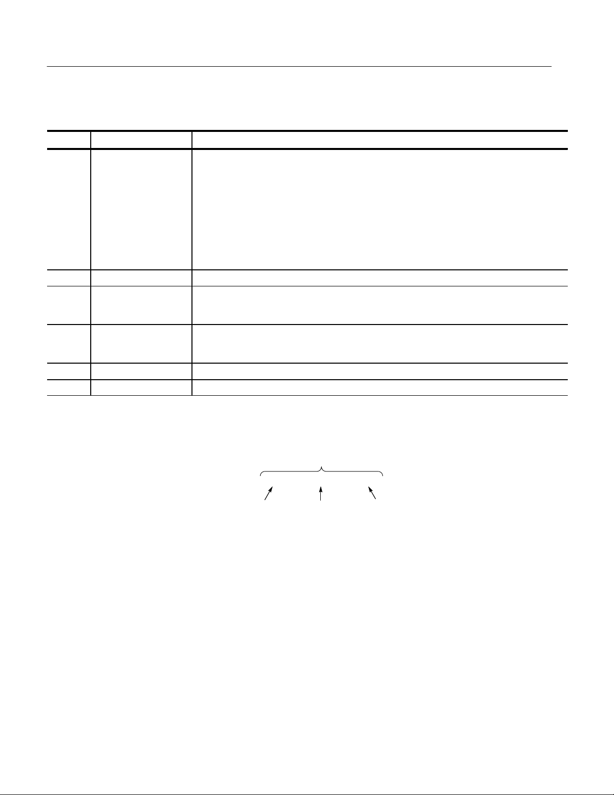
Contacting Tektronix
Product
Support
Service
Support
For other
information
To write us Tektronix, Inc.
For application-oriented questions about a Tektronix measurement product, call toll free in North America:
1-800-TEK-WIDE (1-800-835-9433 ext. 2400)
6:00 a.m. – 5:00 p.m. Pacific time
Or, contact us by e-mail:
tm_app_supp@tek.com
For product support outside of North America, contact your
local Tektronix distributor or sales office.
Contact your local Tektronix distributor or sales office. Or, visit
our web site for a listing of worldwide service locations.
http://www.tek.com
In North America:
1-800-TEK-WIDE (1-800-835-9433)
An operator will direct your call.
P.O. Box 1000
Wilsonville, OR 97070-1000
x
TMS 420 R3051, R3052 & R3081 Microprocessor Support Instruction Manual
Page 14

Getting Started
Support Description
This chapter provides information on the following topics and tasks:
H A description of the TMS 420 microprocessor support package
H Logic analyzer software compatibility
H Your System Under Test (SUT) requirements
H Support restrictions
H How to configure your probe adapter
H How to connect to your SUT
The TMS 420 microprocessor support package disassembles data from systems
that are based on the Intel MIPS R3051, R3052, and R3081 microprocessors and
their “E” versions. The support runs on a compatible Tektronix logic analyzer
equipped with a 102/136-channel module or a 96-channel module.
Refer to information on basic operations to determine how many modules and
probes your logic analyzer needs to meet the minimum channel requirements for
the TMS 420 microprocessor support.
Table 1–1 shows the microprocessors and packages from which the TMS 420
support can acquire and disassemble data.
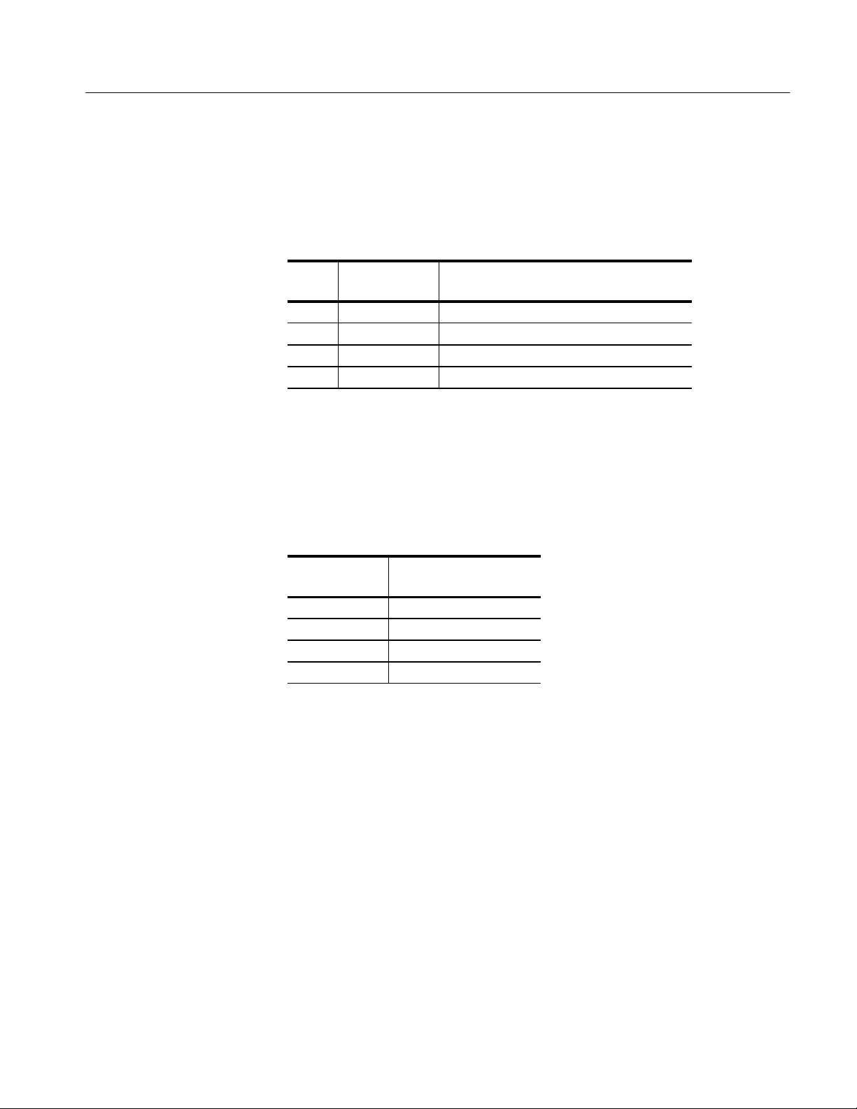
T able 1–1: Supported microprocessors
Name Package
R3051/E PGA, PLCC
R3052/E PGA, PLCC
R3081/E PGA, PLCC
A complete list of standard and optional accessories is provided at the end of the
parts list in the Replaceable Mechanical Parts chapter.
To use this support efficiently, you need to have the items listed in the information on basic operations as well as the R3051, R3052 and R3081 Microprocessor
User’s Manual, Intel, 1991
Information on basic operations also contains a general description of supports.
TMS 420 R3051, R3052 & R3081 Microprocessor Support Instruction Manual
1–1
Page 15

Getting Started
Logic Analyzer Software Compatibility
The label on the microprocessor support floppy disk states which version of logic
analyzer software the support is compatible with.
Logic Analyzer Configuration
To use the TMS 420 support, the Tektronix logic analyzer must be equipped with
either a 102/136-channel module or a 96-channel module at a minimum. The
module must be equipped with enough probes to acquire channel and clock data
from signals in your R3051, R3052 and R3081-based system.
Refer to information on basic operations to determine how many modules and
probes the logic analyzer needs to meet the channel requirements.
Requirements and Restrictions
You should review the general requirements and restrictions of microprocessor
supports in the information on basic operations as they pertain to your SUT.
You should also review electrical, environmental, and mechanical specifications
in the Specifications chapter in this manual as they pertain to your system under
test, as well as the following descriptions of other R3051, R3052 and R3081
support requirements and restrictions.
System Clock Rate. The TMS 420 support can acquire data from the R3051,
R3052 and R3081 microprocessor at speeds of up to 40 MHz
Configuring the Probe Adapter
There are two jumpers on the probe adapter used to turn the cache on or off.
To turn the cache off, place jumpers J1771 and J1672 to the 2-3 position. When
the jumpers are in the 2-3 position, the signal RSVD (2) must be disconnected
from the probe adapter.
To turn the cache on, place jumpers J1771 and J1672 to the 1-2 position. When
the jumpers are in the 1-2 position, the signal RSVD (2) may be reconnected.
1
.
1–2
1
Specification at time of printing. Contact your Tektronix sales representative for
current information on the fastest devices supported.
TMS 420 R3051, R3052 & R3081 Microprocessor Support Instruction Manual
Page 16
Connecting to a System Under Test
Before you connect to the SUT, you must connect the probes to the module.
Your SUT must also have a minimum amount of clear space surrounding the
microprocessor to accommodate the probe adapter. Refer to the Specifications
chapter in this manual for the required clearances.
The channel and clock probes shown in this chapter are for a 102/136-channel
module. The probes will look different if you are using a 96-channel module.
The general requirements and restrictions of microprocessor supports in the
information on basic operations shows the vertical dimensions of a channel or
clock probe connected to square pins on a circuit board.
Getting Started
PGA Probe Adapter
To connect the logic analyzer to a SUT using a PGA probe adapter, follow these
steps:
1. Turn off power to your SUT. It is not necessary to turn off power to the logic
analyzer.
CAUTION. Static discharge can damage the microprocessor, the probe adapter,
the probes, or the module. To prevent static damage, handle all of the above only
in a static-free environment.
Always wear a grounding wrist strap or similar device while handling the
microprocessor and probe adapter.
2. To discharge your stored static electricity, touch the ground connector located
on the back of the logic analyzer. Then, touch any of the ground pins of the
probe adapter to discharge stored static electricity from the probe adapter.
3. Place the probe adapter onto the antistatic shipping foam to support the probe
as shown in Figure 1–1. This prevents the circuit board from flexing and the
socket pins from bending.
4. Remove the microprocessor from your SUT.
5. Line up the pin A1 indicator on the probe adapter board with the pin A1
indicator on the microprocessor.
CAUTION. Failure to correctly place the microprocessor into the probe adapter
might permanently damage the microprocessor once power is applied.
TMS 420 R3051, R3052 & R3081 Microprocessor Support Instruction Manual
1–3
Page 17

Getting Started
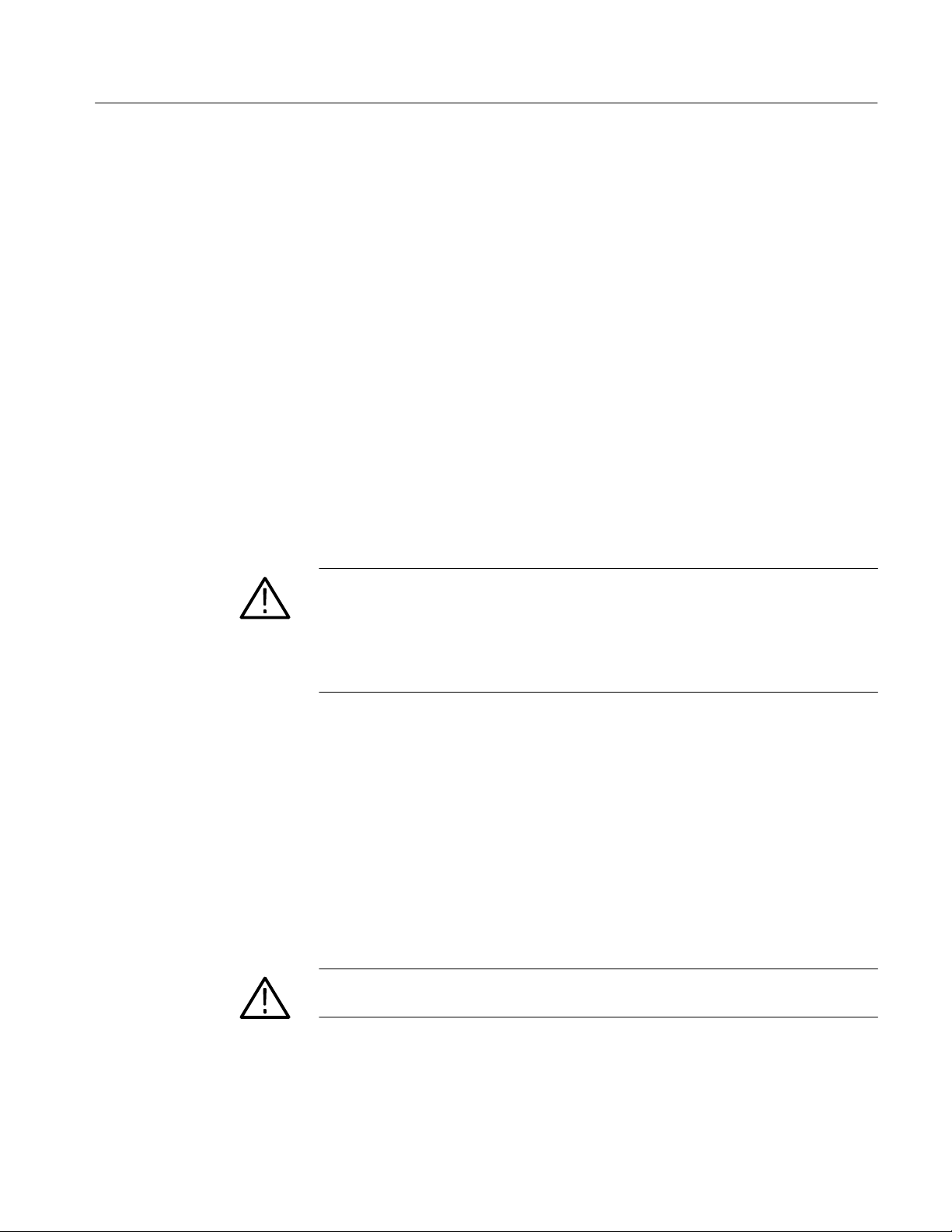
6. Place the microprocessor into the probe adapter as shown in Figure 1–1.
Microprocessor
Probe adapter
Foam
Figure 1–1: Placing a microprocessor into a PGA probe adapter
7. Connect the channel and clock probes to the probe adapter as shown in
Figure 1–2. Match the channel groups and numbers on the probe labels to the
corresponding pins on the probe adapter. Match the ground pins on the
probes to the corresponding pins on the probe adapter.
1–4
TMS 420 R3051, R3052 & R3081 Microprocessor Support Instruction Manual
Page 18
Getting Started
Channel probe
and podlet holder
Hold the channel probes by the podlet
holder when connecting them to the
probe adapter. Do not hold them by
the cables or necks of the podlets.
Foam
Figure 1–2: Connecting probes to a PGA probe adapter
Clock probe
Probe adapter
8. Line up the pin A1 indicator on the probe adapter board with the pin A1
indicator on your SUT.
9. Place the probe adapter onto the SUT as shown in Figure 1–3.
NOTE. You might need to stack one or more replacement sockets between the SUT
and the probe adapter to provide sufficient vertical clearance from adjacent
components. However, keep in mind that this might increase loading, which can
reduce the electrical performance of your probe adapter.
TMS 420 R3051, R3052 & R3081 Microprocessor Support Instruction Manual
1–5
Page 19

Getting Started
SUT socket
PLCC Probe Adapter
Figure 1–3: Placing a PGA probe adapter onto the SUT
To connect the logic analyzer to a SUT using a PLCC probe adapter, follow these
steps:
1. Turn off power to your SUT. It is not necessary to turn off the logic analyzer.
CAUTION. Static discharge can damage the microprocessor, the probe adapter,
the probes, or the module. To prevent static damage, handle all of the above only
in a static-free environment.
Always wear a grounding wrist strap or similar device while handling the
microprocessor and probe adapter.
2. To discharge your stored static electricity, touch the ground connector located
on the back of the logic analyzer. Then, touch any of the ground pins of the
probe adapter to discharge stored static electricity from the probe adapter.
3. Place the probe adapter onto the antistatic shipping foam to support the probe
as shown in Figure 1–4. This prevents the circuit board from flexing.
4. Remove the microprocessor from your SUT.
1–6
TMS 420 R3051, R3052 & R3081 Microprocessor Support Instruction Manual
Page 20

Getting Started
5. Line up the pin 1 indicator on the microprocessor with pin 1 of the PLCC
socket on the probe adapter.
CAUTION. Failure to correctly place the microprocessor into the probe adapter
might permanently damage all electrical components once power is applied.
6. Place the microprocessor into the probe adapter as shown in Figure 1–4.
Microprocessor
Probe adapter
Foam
Bevel at both corners
Figure 1–4: Placing a microprocessor into a PLCC probe adapter
TMS 420 R3051, R3052 & R3081 Microprocessor Support Instruction Manual
1–7
Page 21
Getting Started
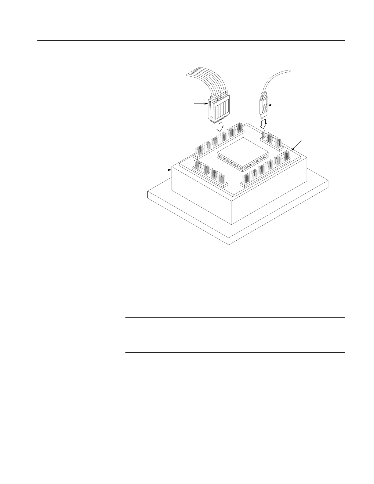
7. Connect the channel and clock probes to the probe adapter as shown in
Figure 1–5. Match the channel groups and numbers on the probe labels to the
corresponding pins on the probe adapter. Match the ground pins on the
probes to the corresponding pins on the probe adapter.
Channel probe
and podlet holder
Hold the channel probes by the podlet
holder when connecting them to the
probe adapter. Do not hold them by
the cables or necks of the podlets.
Foam
Figure 1–5: Connecting probes to a PLCC probe adapter
Clock probe
Probe adapter
1–8
TMS 420 R3051, R3052 & R3081 Microprocessor Support Instruction Manual
Page 22

8. Place the probe adapter onto the SUT as shown in Figure 1–6.
Bevel at both
corners
SUT socket
Getting Started
Without a Probe Adapter
Figure 1–6: Placing a PLCC probe adapter onto the SUT
You can use channel probes, clock probes, and leadsets with a commercial test
clip (or adapter) to make connections between the logic analyzer and your SUT.
To connect the probes to R3051, R3052 and R3081 signals in the SUT using a
test clip, follow these steps:
1. Turn off power to your SUT. It is not necessary to turn off power to the logic
analyzer.
CAUTION. Static discharge can damage the microprocessor, the probes, or the
module. To prevent static damage, handle all of the above only in a static-free
environment.
Always wear a grounding wrist strap or similar device while handling the
microprocessor.
TMS 420 R3051, R3052 & R3081 Microprocessor Support Instruction Manual
1–9
Page 23
Getting Started
2. To discharge your stored static electricity, touch the ground connector located
on the back of the logic analyzer. If you are using a test clip, touch any of the
ground pins on the clip to discharge stored static electricity from it.
CAUTION. Failure to place the SUT on a horizontal surface before connecting the
test clip might permanently damage the pins on the microprocessor.
3. Place the SUT on a horizontal static-free surface.
4. Use Table 1–2 to connect the channel probes to R3051, R3052 and R3081
signal pins on the test clip or in the SUT.
Use leadsets to connect at least one ground lead from each channel probe and
the ground lead from each clock probe to ground pins on your test clip.
NOTE. Since the probe adapter multiplexes address A31-A4 and data D31-D4 (as
the A_D31-A_D4 signals), the D3:7-0, D2:7-0, D1:7-0 and D0:7-4 channel
probes do not need to be connected.
These channels are not considered to be extra channels, even though they are not
connected. Do not use them to make connections to other signals in your SUT.
T able 1–2: R3051, R3052 and R3081 signal connections for channel probes
R3051, R3052 and R3081
Section:channel
A3:7 A_D(31) D3:7 A_D(31) *
A3:6 A_D(30) D3:6 A_D(30) *
A3:5 A_D(29) D3:5 A_D(29) *
A3:4 A_D(28) D3:4 A_D(28) *
A3:3 A_D(27) D3:3 A_D(27) *
A3:2 A_D(26) D3:2 A_D(26) *
A3:1 A_D(25) D3:1 A_D(25) *
A3:0 A_D(24) D3:0 A_D(24) *
A2:7 A_D(23) D2:7 A_D(23) *
A2:6 A_D(22) D2:6 A_D(22) *
A2:5 A_D(21) D2:5 A_D(21) *
signal
Section:channel
R3051, R3052 and R3081
signal
1–10
A2:4 A_D(20) D2:4 A_D(20) *
TMS 420 R3051, R3052 & R3081 Microprocessor Support Instruction Manual
Page 24

Getting Started
T able 1–2: R3051, R3052 and R3081 signal connections for channel probes (cont.)
R3051, R3052 and R3081
Section:channel
A2:3 A_D(19) D2:3 A_D(19) *
A2:2 A_D(18) D2:2 A_D(18) *
A2:1 A_D(17) D2:1 A_D(17) *
A2:0 A_D(16) D2:0 A_D(16) *
A1:7 A_D(15) D1:7 A_D(15) *
A1:6 A_D(14) D1:6 A_D(14) *
A1:5 A_D(13) D1:5 A_D(13) *
A1:4 A_D(12) D1:4 A_D(12) *
A1:3 A_D(1 1) D1:3 A_D(11) *
A1:2 A_D(10) D1:2 A_D(10) *
A1:1 A_D(9) D1:1 A_D(9) *
A1:0 A_D(8) D1:0 A_D(8) *
A0:7 A_D(7) D0:7 A_D(7) *
A0:6 A_D(6) D0:6 A_D(6) *
A0:5 A_D(5) D0:5 A_D(5) *
A0:4 A_D(4) D0:4 A_D(4) *
signal
Section:channel
R3051, R3052 and R3081
signal
A0:3 ADDR(3) D0:3 A_D(3) *
A0:2 ADDR(2) D0:2 A_D(2) *
A0:1 Ground D0:1 A_D(1) *
A0:0 Ground D0:0 A_D(0) *
C3:7 Diag_1 C2:7 BE_1~
C3:6 RdCEn_B~ C2:6 Ack_B~
C3:5 BE_3~ C2:5 BE_0~
C3:4 SysClk_B~ C2:4 Not connected
C3:3 Diag_0 C2:3 Rd~
C3:2 Brst~_W rNr~ C2:2 BusError_L~
C3:1 BE_2~ C2:1 Reset~
C3:0
C1:7
C1:6
C1:5
ALE_B [
SInt_0~ [
SInt_1~ [
SInt_2~ [
C2:0 BusGnt~
C0:7
C0:6
C0:5
BrCond_0 [
Wr~ [
DataEn~ [
TMS 420 R3051, R3052 & R3081 Microprocessor Support Instruction Manual
1–11
Page 25

Getting Started
T able 1–2: R3051, R3052 and R3081 signal connections for channel probes (cont.)
R3051, R3052 and R3081
Section:channel
C1:4
C1:3
C1:2
C1:1
C1:0
* These channels do not have to be connected for disassembly because they are
multiplexed on the probe adapter board.
[ Signal not required for disassembly.
signal
Int_3~ [
Int_4~ [
Int_5~ [
CohReq~ [
Rsvd_1 [
Section:channel
C0:4
C0:3
C0:2
C0:1
C0:0
R3051, R3052 and R3081
signal
BusReq~ [
SBrCond_2 [
BrCond_1 [
Rsvd_2 [
SBrCond_3 [
Table 1–3 shows the clock probes and the R3051, R3052 and R3081 signal to
which they must connect for disassembly to be correct.
T able 1–3: R3051, R3052 and R3081 signal connections for clock
probes
Section:channel R3051, R3052 and R3081 signal
CK:3 SysClk_B~
CK:2 RdCEn_L~
CK:1 Ack_L~
CK:0 ALE_B
5. Align pin 1 or A1 of your test clip with the corresponding pin 1 or A1 of the
R3051, R3052 and R3081 microprocessor in your SUT and attach the clip.
1–12
TMS 420 R3051, R3052 & R3081 Microprocessor Support Instruction Manual
Page 26

Setting Up the Support
This section provides information on how to set up the support. Information
covers the following topics:
H Channel group definitions
H Clocking options
H Symbol table files
Remember that the information in this section is specific to the operations and
functions of the TMS 420 R3051, R3052 and R3081 support on any Tektronix
logic analyzer for which it can be purchased. Information on basic operations
describes general tasks and functions.
Before you acquire and disassemble data, you need to load the support and
specify setups for clocking and triggering as described in the information on
basic operations. The support provides default values for each of these setups,
but you can change them as needed.
Channel Group Definitions
Clocking Options
The software automatically defines channel groups for the support. The channel
groups for the R3051, R3052 and R3081 support are Address, Data, Control,
DataSize, Timing, MiscCtrl, Intr, Debug, and Conds. If you want to know which
signal is in which group, refer to the channel assignment tables beginning on
page 3–6.
The TMS 420 support offers a microprocessor-specific clocking mode for the
R3051, R3052 and R3081 microprocessor. This clocking mode is the default
selection whenever you load the R3051 support.
A description of how cycles are sampled by the module using the support and
probe adapter is found in the Specifications chapter.
Disassembly will not be correct with the Internal or External clocking modes.
Information on basic operations describes how to use these clock selections for
general purpose analysis.
The clocking options for the TMS 420 support are: DMA Cycles and Probe
Interface Type.
TMS 420 R3051, R3052 & R3081 Microprocessor Support Instruction Manual
2–1
Page 27

Setting Up the Support
Á
Á
Á
Á
Á
Á
Probe Interface Type
Symbols
DMA Cycles
A DMA cycle is defined as the cycle in which the R3051, R3052 and R3081
microprocessor gives up the bus to an alternate device (a DMA device or another
microprocessor). These types of cycles are acquired when you select Included.
You must use the TMS 420
probe adapter to acquire data from R3051, R3052
and R3081 microprocessor-based systems running at speeds to 40 MHz. When
using the probe adapter, you must select With Probe Adapter in this field.
You can also connect the podlets directly to your SUT. However, the support
speed is reduced from 40 to 33 MHz. If connecting directly to your SUT, you
must select Without Probe Adapter in this field.
The TMS 420 support supplies one symbol table file. The R3051_Ctrl file
replaces specific Control channel group values with symbolic values when
Symbolic is the radix for the channel group.
Table 2–1 shows the name, bit pattern, and meaning for the symbols in the file
R3051_Ctrl, the Control channel group symbol table.
T able 2–1: Control group symbol table definitions
Symbol
ÁÁÁÁ
ÁÁÁÁ
Control group value
RD~
Brst_WrNr~ BusGnt~
Diag_1 Reset~
Diag_0 BusError~
ББББББББ
ББББББББ
Meaning
Data Cache Read
Instruction Cache Read
Data Cache Burst Read
БББББББББ
Instruction Cache Burst Read
Mem Read I/D
Mem Write
Mem Write Near
DMA Read
DMA Write
DMA Read Buserror
DMA Write Buserror
БББББББББ
Read Buserror
Write Buserror
Reset
2–2
TMS 420 R3051, R3052 & R3081 Microprocessor Support Instruction Manual
Page 28

Setting Up the Support
Table 2–2 shows the name, bit pattern, and meaning for the symbols in the file
R3051_Size, the DataSize channel group symbol table.
T able 2–2: DataSize group symbol table definitions
DataSize group value
BE(3)~
BE(2)~
Symbol
BE(1)~
BE(0)~
Information on basic operations describes how to use symbolic values for
triggering and for displaying other channel groups symbolically, such as the
Address channel group.
TMS 420 R3051, R3052 & R3081 Microprocessor Support Instruction Manual
2–3
Page 29

Acquiring and Viewing Disassembled Data
This section describes how to acquire data and view it disassembled. Information
covers the following topics and tasks:
H Acquiring data
H Viewing disassembled data in various display formats
H Cycle type labels
H Changing the way data is displayed
H Changing disassembled cycles with the mark cycles function
Acquiring Data
Once you load the R3051 support, choose a clocking mode, and specify the
trigger, you are ready to acquire and disassemble
If you have any problems acquiring data, refer to information on basic operations
in your online help or Appendix A: Error Messages and Disassembly Problems in
the basic operations user manual.
data.
Viewing Disassembled Data
You can view disassembled data in four display formats: Hardware, Software,
Control Flow, and Subroutine. The information on basic operations describes
how to select the disassembly display formats.
NOTE. Selections in the Disassembly property page (the Disassembly Format
Definition overlay) must be set correctly for your acquired data to be disassembled correctly. Refer to Changing How Data is Displayed on page 2–8.
The default display format shows the Address, Data, and Control channel group
values for each sample of acquired data.
The disassembler displays special characters and strings in the instruction
mnemonics to indicate significant events. Table 2–3 shows these special
characters and strings, and gives a definition of what they represent.
TMS 420 R3051, R3052 & R3081 Microprocessor Support Instruction Manual
2–5
Page 30

Acquiring and Viewing Disassembled Data
T able 2–3: Meaning of special characters in the display
Character or string displayed Meaning
or m
The instruction was manually marked
Hardware Display Format
****
Indicates there is insufficient data available for complete
disassembly of the instruction; the number of asterisks
indicates the width of the data that is unavailable. Each two
asterisks represent one byte.
In Hardware display format, the disassembler displays certain cycle type labels in
parentheses. Table 2–4 shows these cycle type labels and gives a definition of the
cycle they represent. Reads to interrupt and exception vectors will be labeled
with the vector name.
T able 2–4: Cycle type definitions
Cycle type Definition
( DATA CACHE READ )
( DATA CACHE BURST READ )
( MEM READ )
( MEM WRITE )
( MEMORY WRITE NEAR )
( DMA READ )
( DMA WRITE )
Single word read into the data cache
Quad word read burst into data cache
Single word read from memory
Single word write into memory
Single word write into adjacent memory locations
DMA device has control of CPU bus for reading data
DMA device has control of CPU bus for writing data
2–6
( DMA READ BUS ERROR )
( DMA WRITE BUS ERROR )
( CPU READ BUS ERROR )
( CPU WRITE BUS ERROR )
( CPU RESET )
** INVALID BUS CYCLE **
* Computed cycle types.
DMA read bus error detected
DMA write bus error detected
CPU read bus error detected
CPU write bus error detected
CPU reset initiated
The combinations of control bits is unexpected and/or
unrecognized
TMS 420 R3051, R3052 & R3081 Microprocessor Support Instruction Manual
Page 31

Acquiring and Viewing Disassembled Data
Figure 2–1 shows an example of the Hardware display.
1 2 3 4 5
Sample Address Data Mnemonics Control Timest>
-------------------------------------------------------------------------------T 0 00000CE4------------(-CPU-RESET-)-------------------RESET-------------
1 1FC00000 0BF00088 J 1FC00220 MEM_RDI/D 480 ns
2 1FC00004 00000000 NOP MEM_RDI/D 440 ns
3 1FC00220 3C022010 LUI V0,2010 MEM_RDI/D 440 ns
4 1FC00224 40826000 MTC0 V0,SR MEM_RDI/D 440 ns
5 1FC00228 40806800 MTC0 ZERO,CAUSE MEM_RDI/D 440 ns
6 1FC0022C 3C02A000 LUI V0,A000 MEM_RDI/D 440 ns
7 1FC00230 3C08AAAA LUI T0,AAAA MEM_RDI/D 440 ns
8 1FC00234 35085555 ORI T0,T0,5555 MEM_RDI/D 440 ns
9 1FC00238 AC480000 SW T0,0000(V0) MEM_RDI/D 440 ns
10 1FC0023C AC400004 SW ZERO,0004(V0) MEM_RDI/D 440 ns
11 00000000 AAAA5555 ( MEM WRITE ) MEM_WRITE 360 ns
12 1FC00240 8C490000 LW T1,0000(V0) MEM_RDI/D 320 ns
13 00000004 00000000 ( MEM WRITE ) MEM_WRITE 360 ns
14 1FC00244 00000000 NOP MEM_RDI/D 320 ns
15 00000000 AAAA5555 ( MEM READ ) MEM_RDI/D 360 ns
16 1FC00248 11280003 BEQ T1,T0,1FC00258 MEM_RDI/D 440 ns
17 1FC0024C 00000000 NOP MEM_RDI/D 440 ns
18 1FC00258 2408FFFF ADDIU T0,ZERO,FFFF MEM_RDI/D 440 ns
19 1FC0025C AC480008 SW T0,0008(V0) MEM_RDI/D 440 ns
20 1FC00260 AC400004 SW ZERO,0004(V0) MEM_RDI/D 440 ns
6
Figure 2–1: Hardware display format
1
Sample Column. Lists the memory locations for the acquired data.
2
Address Group. Lists data from channels connected to the R3051, R3052
and R3081 address bus.
3
Data Group. Lists data from channels connected to the R3051, R3052 and
R3081 data bus.
4
Mnemonics Column. Lists the disassembled instructions and cycle types.
5
Control Group. Lists data from channels connected to R3051, R3052 and
R3081 microprocessor control signals ( shown symbolically).
6
Timestamp. Lists the timestamp values when a timestamp selection is made.
Information on basic operations describes how you can select a timestamp.
TMS 420 R3051, R3052 & R3081 Microprocessor Support Instruction Manual
2–7
Page 32

Acquiring and Viewing Disassembled Data
Software Display Format
Control Flow Display
Format
Subroutine Display
Format
The Software display format shows only the first fetch of executed instructions.
Flushed cycles and extensions are not shown, even though they are part of the
executed instruction. Read extensions will be used to disassemble the instruction,
but will not be displayed as a separate cycle in the Software display format. Data
reads and writes are not displayed.
The Control Flow display format shows only the first fetch of instructions that
change the flow of control.
Instructions that generate a change in the flow of control in the R3051, R3052
and R3081 microprocessor are as follows:
BCzF BGEZ BLTZ JR except R31
BCzT BGTZ BNE J
BEQ BLEZ
The Subroutine display format shows only the first fetch of subroutine call and
return instructions. It will display conditional subroutine calls if they are
considered to be taken.
Instructions that generate a subroutine call or a return in the R3051, R3052 and
R3081 microprocessor are as follows:
BGEZAL BREAK JALR RFE
BLTZAL JAL JR R31 SYSCALL
Changing How Data is Displayed
There are common fields and features that allow you to further modify displayed
data to suit your needs. You can make common and optional display selections in
the Disassembly property page (the Disassembly Format Definition overlay).
You can make selections unique to the R3051, R3052 and R3081 support to do
the following tasks:
H Change how data is displayed across all display formats
H Change the interpretation of disassembled cycles
Optional Display
Selections
You can make optional selections for disassembled
common selections (described in the information on basic operations), you can
change the displayed data in the following ways:
H Select the type of CPU general registers
H Mark invalid bytes in the Data channel group
data. In addition to the
2–8
TMS 420 R3051, R3052 & R3081 Microprocessor Support Instruction Manual
Page 33

Acquiring and Viewing Disassembled Data
The R3051, R3052 and R3081 support has two additional fields: CPU Regs and
Data Bytes. These fields appear in the area indicated in the information on basic
operations.
CPU Regs. You can select the names of the CPU general registers as either
Software or Hardware.
Data Bytes. Marks invalid bytes within the Data group. You can choose to Mark
Invalid Data or Display All Data.
Marking Cycles
The disassembler has a Mark Opcode function that allows you to change the
interpretation of a cycle type. Using this function, you can select a cycle and
change it to one of the following cycle types:
H Opcode (the first word of an instruction)
H Read (marks a memory reference read as data)
Mark selections are as follows:
OPCODE
Read
Undo marks on this cycle
Information on basic operations contains more details on marking cycles.
Viewing an Example of Disassembled Data
A demonstration system file (or demonstration reference memory) is provided so
you can see an example of how your R3051, R3052 and R3081 microprocessor
bus cycles and instruction mnemonics look when they are disassembled. Viewing
the system file is not a requirement for preparing the module for use and you can
view it without connecting the logic analyzer to your SUT.
Information on basic operations describes how to view the file.
TMS 420 R3051, R3052 & R3081 Microprocessor Support Instruction Manual
2–9
Page 34

Specifications
This chapter contains the following information:
H Probe adapter description
H Specification tables
H Dimensions of the probe adapter
H Channel assignment tables
H Description of how the module acquires R3051, R3052 and R3081 signals
H List of other accessible microprocessor signals and extra probe channels
Probe Adapter Description
The probe adapter is nonintrusive hardware that allows the logic analyzer to
acquire data from a microprocessor in its own operating environment with little
effect, if any, on that system. Information on basic operations contains a figure
showing the logic analyzer connected to a typical probe adapter. Refer to that
figure while reading the following description.
Configuration
The probe adapter consists of a circuit board and a socket for a R3051, R3052
and R3081 microprocessor. The probe adapter connects to the microprocessor in
the SUT. Signals from the microprocessor-based system flow from the probe
adapter to the channel groups and through the probe signal leads to the module.
All circuitry on the probe adapter is powered from the SUT.
One probe adapter accommodates the Intel MIPS R3051, R3052 and R3081
microprocessor in a 84-pin PGA package.
the R3051, R3052 and R3081 microprocessor in an 84-pin PLCC package.
There are two jumpers on the probe adapter used to turn the cache on or off.
To turn the cache off, place jumpers J1771 and J1671 to the 2-3 position. When
the jumpers are in the 2-3 position, the signal RSVD (2) must be disconnected
from the probe adapter.
To turn the cache on, place jumpers J1771 and J1671 to the 1-2 position. When
the jumpers are in the 1-2 position, the signal RSVD (2) may be reconnected.
A second probe adapter accommodates
TMS 420 R3051, R3052 & R3081 Microprocessor Support Instruction Manual
3–1
Page 35

Specifications
Specifications
These specifications are for a probe adapter connected between a compatible
Tektronix logic analyzer and a SUT. Table 3–1 shows the electrical requirements
the SUT must produce for the support to acquire correct data.
In Table 3–1, for the 102/136-channel module, one podlet load is 20 k in
parallel with 2 pF. For the 96-channel module, one podlet load is 100 k in
parallel with 10 pF.
T able 3–1: Electrical specifications
Characteristics Requirements
SUT DC power requirements
Voltage 4.75-5.25 VDC
Current I maximum 455 mA
I typical 350 mA
SUT clock
Clock rate Maximum 33 MHz
(40 MHz with probe adapter)
Minimum setup time required
All signals 4 ns
Minimum hold time required
All signals 4 ns
Specification
Measured typical SUT signal loading AC load DC load
A_D (31-4) 4 pF + 1 podlet 1 podlet
A_D (3-0) 10 pF + 2 podlets 2 podlets
Rd~, Daig_(1-0),
Busrst~_WrNr~, Addr_(1-0),
ALE
RdCEn~, Ack~, BusError~ 11 pF 16R4-4 PLCC
BRcond (1-0), Sint_(0-2),
Int_(3-5), SBrcond_(3-2)
Rsvd_(1-2), BusBnt~, Reset~ 9 pF 1 podlet
SYSCLK~
[
This does not include the transmission line termination network of 100 pF in series
with 100 . With good clock signal quality you can remove the network to improve
signal quality.
12 pF 74FR244
11 pF 16L8-5 in parallel
with podlet
10 pF
[
74FR244
3–2
TMS 420 R3051, R3052 & R3081 Microprocessor Support Instruction Manual
Page 36

Table 3–2 shows the environmental specifications.
T able 3–2: Environmental specifications*
Characteristic Description
Temperature
Specifications
Maximum operating
Minimum operating 0° C (+32° F)
Non-operating –55° to +75° C (–67° to +167° F)
Humidity 10 to 95% relative humidity
Altitude
Operating 4.5 km (15,000 ft) maximum
Non-operating 15 km (50,000 ft) maximum
Electrostatic immunity The probe adapter is static sensitive
* Designed to meet Tektronix standard 062-2847-00 class 5.
[
Not to exceed R3051, R3052 and R3081 microprocessor thermal considerations.
Forced air cooling might be required across the CPU.
+50° C (+122° F)[
Table 3–3 shows the certifications and compliances that apply to the probe
adapter.
T able 3–3: Certifications and compliances
EC Compliance There are no current European Directives that apply to this product.
TMS 420 R3051, R3052 & R3081 Microprocessor Support Instruction Manual
3–3
Page 37

Specifications
Figure 3–1 shows the dimensions of the PGA probe adapter. Information on basic
operations shows the vertical clearance of the channel and clock probes when
connected to a probe adapter.
90 mm
(3.000 in)
17 mm
(.650 in)
17 mm
(.650 in)
90 mm
2.800 in
PIN A1
3–4
7 mm (.26 in)
Figure 3–1: Dimensions of the PGA probe adapter
TMS 420 R3051, R3052 & R3081 Microprocessor Support Instruction Manual
Page 38

Specifications
Figure 3–2 shows the dimensions of the PLCC probe adapter. Information on
basic operations shows the vertical clearance of the channel and clock probes
when connected to a probe adapter.
90 mm
(3.000 in)
29 mm
(1.150 in)
31 mm
(1.250 in)
PIN 1
90 mm
(2.800 in)
9 mm
(.340 in)
Figure 3–2: Dimensions of the probe adapter
TMS 420 R3051, R3052 & R3081 Microprocessor Support Instruction Manual
3–5
Page 39

Specifications
Channel Assignments
Channel assignments shown in Table 3–4 through Table 3–13 use the following
conventions:
H All signals are required by the support unless indicated otherwise.
H Channels are shown starting with the most significant bit (MSB) descending
to the least significant bit (LSB).
H Channel group assignments are for all modules unless otherwise noted.
H A tilde (~) following a signal name indicates an active low signal.
Table 3–4 shows the probe section and channel assignments for the Address
group and the microprocessor signal to which each channel connects. By default,
this channel group is displayed in hexadecimal.
T able 3–4: Address group channel assignments
Bit
order
31 A3:7 A_D31(31)
30 A3:6 A_D30(30)
29 A3:5 A_D29(29)
28 A3:4 A_D28(28)
27 A3:3 A_D27(27)
26 A3:2 A_D26(26)
25 A3:1 A_D25(25)
24 A3:0 A_D24(24)
23 A2:7 A_D23(23)
22 A2:6 A_D22(22)
21 A2:5 A_D21(21)
20 A2:4 A_D20(20)
19 A2:3 A_D19(19)
18 A2:2 A_D18(18)
17 A2:1 A_D17(17)
16 A2:0 A_D16(16)
15 A1:7 A_D15(15)
14 A1:6 A_D14(14)
13 A1:5 A_D13(13)
12 A1:4 A_D12(12)
11 A1:3 A_D11(11)
10 A1:2 A_D10(10)
9 A1:1 A_D9(9)
Section:channel R3051, R3052 and R3081 signal name
3–6
TMS 420 R3051, R3052 & R3081 Microprocessor Support Instruction Manual
Page 40

Specifications
T able 3–4: Address group channel assignments
Bit
order
8 A1:0 A_D8(8)
7 A0:7 A_D7(7)
6 A0:6 A_D6(6)
5 A0:5 A_D5(5)
4 A0:4 A_D4(4)
3 A0:3 ADDR(3)
2 A0:2 ADDR(2)
1 A0:1 Ground
0 A0:0 Ground
R3051, R3052 and R3081 signal nameSection:channel
Table 3–5 shows the probe section and channel assignments for the Data group
and the microprocessor signal to which each channel connects. By default, this
channel group is displayed in hexadecimal.
NOTE. Since the probe adapter multiplexes address A31-A4 and data D31-D4 (as
the A_D31-A_D4 signals), the D3:7-0, D2:7-0, D1:7-0 and D0:7-4 channel
probes do not need to be connected.
These channels are not considered to be extra channels, even though they are not
connected. Do not use them to make connections to other signals in your SUT.
T able 3–5: Data group channel assignments
Bit
order
31 D3:7 A_D31(31) *
30 D3:6 A_D30(30) *
29 D3:5 A_D29(29) *
28 D3:4 A_D28(28) *
27 D3:3 A_D27(27) *
26 D3:2 A_D26(26) *
25 D3:1 A_D25(25) *
24 D3:0 A_D24(24) *
23 D2:7 A_D23(23) *
22 D2:6 A_D22(22) *
21 D2:5 A_D21(21) *
20 D2:4 A_D20(20) *
Section:channel R3051, R3052 and R3081 signal name
TMS 420 R3051, R3052 & R3081 Microprocessor Support Instruction Manual
3–7
Page 41

Specifications
T able 3–5: Data group channel assignments
Bit
order
19 D2:3 A_D19(19) *
18 D2:2 A_D18(18) *
17 D2:1 A_D17(17) *
16 D2:0 A_D16(16) *
15 D1:7 A_D15(15) *
14 D1:6 A_D14(14) *
13 D1:5 A_D13(13) *
12 D1:4 A_D12(12) *
11 D1:3 A_D11(1 1) *
10 D1:2 A_D10(10) *
9 D1:1 A_D9(9) *
8 D1:0 A_D8(8) *
7 D0:7 A_D7(7) *
6 D0:6 A_D6(6) *
5 D0:5 A_D5(5) *
4 D0:4 A_D4(4) *
3 D0:3 A_D3(3) *
2 D0:2 A_D2(2) *
1 D0:1 A_D1(1) *
0 D0:0 A_D0(0) *
* These channels do not have to be connected for disassembly
because they are multiplexed on the probe adapter board.
R3051, R3052 and R3081 signal nameSection:channel
3–8
Table 3–6 shows the probe section and channel assignments for the Control
group and the microprocessor signal to which each channel connects. By default,
this channel group is displayed symbolically.
T able 3–6: Control group channel assignments
Bit
order
6 C2:3 Rd~
5 C3:2 Brst~_W rNr~
4 C3:7 Diag_1
3 C3:3 Diag_0
2 C2:0 BusGnt~
Section:channel R3051, R3052 and R3081 signal name
TMS 420 R3051, R3052 & R3081 Microprocessor Support Instruction Manual
Page 42

Specifications
T able 3–6: Control group channel assignments (cont.)
Bit
order
1 C2:1 Reset~
0 C2:2 BusError_L~
R3051, R3052 and R3081 signal nameSection:channel
Table 3–7 shows the probe section and channel assignments for the DataSize
group and the microprocessor signal to which each channel connects. By default,
this channel group is displayed in binary.
T able 3–7: DataSize group channel assignments
Bit
order
3 C3:5 BE_3~
2 C3:1 BE_2~
1 C2:7 BE_1~
0 C2:5 BE_0~
Section:channel R3051, R3052 and R3081 signal name
Table 3–8 shows the probe section and channel assignments for the Timing group
and the microprocessor signal to which each channel connects. By default, this
channel group is displayed in binary.
T able 3–8: Timing group channel assignments
Bit
order
3 C3:4 SysClk_B~
2 C3:0 ALE_B~ *
1 C2:6 Ack_B~
0 C3:6 RdCEn_B~
* Signal not required for disassembly
Section:channel R3051, R3052 and R3081 signal name
TMS 420 R3051, R3052 & R3081 Microprocessor Support Instruction Manual
3–9
Page 43

Specifications
Table 3–9 shows the probe section and channel assignments for the MiscCtrl
group and the microprocessor signal to which each channel connects. By default,
this channel group is not visible.
T able 3–9: MiscCtrl group channel assignments
Bit
order
3 C0:6 Wr~ *
2 C0:5 DataEn~ *
1 C0:4 BusReq~ *
0 C1:1 CohReq~ *
* Signal not required for disassembly.
Section:channel R3051, R3052 and R3081 signal name
Table 3–10 shows the probe section and channel assignments for the Intr group
and the microprocessor signal to which each channel connects. By default, this
channel group is not visible.
T able 3–10: Intr group channel assignments
Bit
order
5 C1:2 Int_5~ *
4 C1:3 Int_4~ *
3 C1:4 Int_3~ *
2 C1:5 Sint_2~ *
1 C1:6 Sint_1~ *
0 C1:7 Sint_0~ *
* Signal not required for disassembly.
Section:channel R3051, R3052 and R3081 signal name
Table 3–11 shows the probe section and channel assignments for the Debug
group and the microprocessor signal to which each channel connects. By default,
this channel group is not visible.
T able 3–11: Debug group channel assignments
Bit
order
1 C0:1 Rsvd_2 *
0 C1:0 Rsvd_1 *
* Signal not required for disassembly.
Section:channel R3051, R3052 and R3081 signal name
3–10
TMS 420 R3051, R3052 & R3081 Microprocessor Support Instruction Manual
Page 44
Specifications
Table 3–12 shows the probe section and channel assignments for the Conds
group and the microprocessor signal to which each channel connects. By default,
this channel group is not visible.
T able 3–12: Conds group channel assignments
Bit
order
3 C0:0 SBrCond_3 *
2 C0:3 SBrCond_2 *
1 C0:2 BrCond_1 *
0 C0:7 BrCond_0 *
* Signal not required for disassembly.
Section:channel R3051, R3052 and R3081 signal name
Table 3–13 shows the probe section and channel assignments for the clock probes
(not part of any group) and the R3051, R3052 and R3081 signal to which each
channel connects.
How Data is Acquired
Custom Clocking
T able 3–13: Clock channel assignments
R3051, R3052 and
Section:channel
CK:3 SysClk_B~
CK:2 RdCEn_L~
CK:1 Ack_L~
CK:0 ALE_B
R3081 signal name
This part of this chapter explains how the module acquires R3051, R3052 and
R3081 signals using the TMS 420 software and probe adapter. This part also
provides additional information on microprocessor signals accessible on or not
accessible on the probe adapter, and on extra probe channels available for you to
use for additional connections.
A special clocking program is loaded to the module every time you load the
R3051 support. This special clocking is called Custom.
With Custom clocking, the module logs in signals from multiple groups of
channels at different times as they become valid on the R3051, R3052 and R3081
bus. The module then sends all the logged-in signals to the trigger machine and
to the memory of the module for storage.
TMS 420 R3051, R3052 & R3081 Microprocessor Support Instruction Manual
3–11
Page 45

Specifications
In Custom clocking, the module clocking state machine (CSM) generates one
master sample for each microprocessor bus cycle, no matter how many clock
cycles are contained in the bus cycle.
Figure 3–3 shows the sample points and the master sample point.
Most R3051 signals are acquired on the falling edge of SYSCLK. The nine
signals that do not become active at that time are hardware latched and shifted to
the falling edge shown in Figure 3–3.
SYSCLK~
ALE
RDCEN~ or ACK~
Address Lines
A/D(31–4)
ADDR (1–0)
Diag_0
Diag_1
Rd~
Reset~
Addr (2–3)
BE_3~ (A/D(3))
BE_2~ (A/D(2))
BE_1~ (A/D(1))
BE_0~ (A/D(0))
Ack~
RdCEn~
BusError”
Data
Sysclk_B”
ALE_B
INT_D”
BUS Gnt~
Brst~_WrNr~
Hardware latched
on probe adapter
Figure 3–3: R3051, R3052 and R3081 bus timing with a probe adapter
If you choose to use Without Probe Adapter, both edges of Sysclk_B~ are used
for clocking. Therefore, there is no need for hardware latches. The effect is lower
clock speed support. Figure 3–4 shows the timing when not using the probe
adapter.
3–12
TMS 420 R3051, R3052 & R3081 Microprocessor Support Instruction Manual
Page 46

SYSCLK~
ALE
RDCEN~ or ACK~
Specifications
Clocking Options
Address Lines
A/D(31–4)
ADDR (1–0)
Diag_0
Diag_1
Rd~
Reset~
Addr (2–3)
BE_3~ (A/D(3))
BE_2~ (A/D(2))
BE_1~ (A/D(1))
BE_0~ (A/D(0))
Ack~
RdCEn~
BusError~
Data
Sysclk_B”
ALE_B
INT_D”
BUS Gnt~
Brst~_WrNr~
Figure 3–4: R3051, R3052 and R3081 bus timing without a probe adapter
The clocking algorithm for the R3051, R3052 and R3081 support has two
variations: Probe Interface Type and DMA Cycles.
One clock option establishes the type of bus cycles to include in or exclude from
the acquisition. The second clock option tells the disassembler weather or not the
probe adapter is being used.
Probe Interface T ype With a Probe Adapter. The probe adapter is being used.
Probe Interface T ype Without a Probe Adapter. The probe adapter is not being
used.
DMA Cycles Excluded. Whenever the HLDA signal is high, no bus cycles are
logged in. Only bus cycles initiated by the R3051, R3052 and R3081 microprocessor (HLDA low) will be logged in. Backoff cycles (caused by the BOFF#
signal) are stored.
DMA Cycles Included. All bus cycles, including DMA cycles and Backoff cycles,
are logged in.
Alternate Microprocessor Connections
You can connect to other signals that are not required by the support so that you
can analyze other signal activity in your system. These signals might or might
TMS 420 R3051, R3052 & R3081 Microprocessor Support Instruction Manual
3–13
Page 47

Specifications
not be accessible on the probe adapter board. The following paragraphs and
tables list signals that are or are not accessible on the probe adapter board.
For a list of signals required or not required for disassembly, refer to the channel
assignment tables beginning on page 3–6. Remember that these channels are
already included in a channel group. If you do connect these channels to other
signals, you should set up another channel group for them.
Signals Not On the Probe
Adapter
Extra Channels
The probe adapter does not provide access for the following microprocessor
signals:
H RSVD3
H RSVD4
H CLKIN
Table 3–14 lists extra sections and channels that are left after you have connected
all the probes used by the support. You can use these extra channels to make
alternate SUT connections.
Channels not defined in a channel group by the TMS 420 software are logged in
with the Master sample point.
T able 3–14: Extra module sections and channels
Module Section: channels
102-channels Qual:1, Qual:0, C2:4
136-channels E3:7-0, E2:7-0, E1:7-0, E0:7-0, Qual:3-0, C2:4
96-channels C2:4
3–14
These channels are not defined in any channel group and data acquired from
them is not displayed. To display data, you will need to define a channel group.
TMS 420 R3051, R3052 & R3081 Microprocessor Support Instruction Manual
Page 48

Maintenance
This chapter contains a circuit description of the probe adapter.
Probe Adapter Circuit Description
The 16R4 is used to latch three rising edge signals for disassembly and to buffer
these signals to reduce loading on the CPU. The 16L8 is used to OR the interrupt
lines for the module. The 74FR244 minimizes the load on the user clock and
buffers other signals to keep the clock/signal timing relation the same.
J1771 and J1671 are used to turn off the cache. The SUT drives these lines,
therefore the SUT driver must be disabled to use this option.
Replacing Signal Leads
Information on basic operations describes how to replace signal leads (individual
channel and clock probes).
Replacing Protective Sockets
Information on basic operations describes how to replace protective sockets.
TMS 420 R3051, R3052 & R3081 Microprocessor Support Instruction Manual
4–1
Page 49

Replaceable Electrical Parts
This chapter contains a list of the replaceable electrical components for the
TMS 420 R3051, R3052 and R3081 microprocessor support. Use this list to
identify and order replacement parts.
Parts Ordering Information
Replacement parts are available through your local Tektronix field office or
representative.
Changes to Tektronix products are sometimes made to accommodate improved
components as they become available and to give you the benefit of the latest
improvements. Therefore, when ordering parts, it is important to include the
following information in your order:
H Part number
H Instrument type or model number
H Instrument serial number
H Instrument modification number, if applicable
If you order a part that has been replaced with a different or improved part, your
local Tektronix field office or representative will contact you concerning any
change in part number.
Change information, if any, is located at the rear of this manual.
Using the Replaceable Electrical Parts List
The tabular information in the Replaceable Electrical Parts List is arranged for
quick retrieval. Understanding the structure and features of the list will help you
find all of the information you need for ordering replacement parts. The
following table describes each column of the electrical parts list.
TMS 420 R3051, R3052 & R3081 Microprocessor Support Instruction Manual
5–1
Page 50
Replaceable Electrical Parts
Parts list column descriptions
Column Column name Description
1 Component number The component number appears on diagrams and circuit board illustrations, located in the diagrams
section. Assembly numbers are clearly marked on each diagram and circuit board illustration in the
Diagrams section, and on the mechanical exploded views in the Replaceable Mechanical Parts list
section. The component number is obtained by adding the assembly number prefix to the circuit
number (see Component Number illustration following this table).
The electrical parts list is arranged by assemblies in numerical sequence (A1, with its subassemblies
and parts, precedes A2, with its subassemblies and parts).
Chassis-mounted parts have no assembly number prefix, and they are located at the end of the
electrical parts list.
2 Tektronix part number Use this part number when ordering replacement parts from Tektronix.
3 and 4 Serial number Column three indicates the serial number at which the part was first effective. Column four indicates
the serial number at which the part was discontinued. No entry indicates the part is good for all serial
numbers.
5 Name & description An item name is separated from the description by a colon (:). Because of space limitations, an item
name may sometimes appear as incomplete. Use the U.S. Federal Catalog handbook H6-1 for
further item name identification.
6 Mfr. code This indicates the code number of the actual manufacturer of the part.
7 Mfr. part number This indicates the actual manufacturer’ s or vendor’s part number .
Abbreviations
Component Number
List of Assemblies
Chassis Parts
Mfr. Code to Manufacturer
Cross Index
Abbreviations conform to American National Standard ANSI Y1.1–1972.
Component number
A23A2R1234 A23 R1234
Assembly number Circuit number
Read: Resistor 1234 (of Subassembly 2) of Assembly 23
A2
Subassembly number
(optional)
A list of assemblies is located at the beginning of the electrical parts list. The
assemblies are listed in numerical order. When a part’s complete component
number is known, this list will identify the assembly in which the part is located.
Chassis-mounted parts and cable assemblies are located at the end of the
Replaceable Electrical Parts List.
The table titled Manufacturers Cross Index shows codes, names, and addresses of
manufacturers or vendors of components listed in the parts list.
5–2
TMS 420 R3051, R3052 & R3081 Microprocessor Support Instruction Manual
Page 51

Manufacturers cross index
Mfr.
code
00779 AMP INC 2800 FULLING MILL
04222 AVX CERAMICS
50434 HEWLETT–PACKARD CO
91637 DALE ELECTRONICS INC 2064 12TH AVE
80009 TEKTRONIX INC 14150 SW KARL BRAUN DR
Manufacturer Address City , state, zip code
PO BOX 3608
DIV OF AVX CORP
OPTOELECTRONICS DIV
19TH AVE SOUTH
P O BOX 867
370 W TRIMBLE RD SAN JOSE CA 95131
PO BOX 609
PO BOX 500
Replaceable Electrical Parts
HARRISBURG PA 17105
MYRTLE BEACH SC 29577
COLUMBUS NE 68601–3632
BEAVERT ON, OR 97077–0001
TMS 420 R3051, R3052 & R3081 Microprocessor Support Instruction Manual
5–3
Page 52

Replaceable Electrical Parts
Replaceable electrical parts list
Component
number
A01 671–2691–00 ADAPTER CIRCUIT BD ASSY: R3051/52/81 PROBE 80009 671269100
A01C2500 283–5004–00 CAP,FXD,CER DI:0.1UF,10%,25V 04222 12063C104KAT3A
A01C2600 283–5004–00 CAP,FXD,CER DI:0.1UF,10%,25V 04222 12063C104KAT3A
A01C2800 283–5188–00 CAP,FXD,CER DI:100PF,5%,100V 04222 12061A0101JAT1A
A01C4700 283–5188–00 CAP,FXD,CER DI:100PF,5%,100V 04222 12061A0101JAT1A
A01C6100 283–5004–00 CAP,FXD,CER DI:0.1UF,10%,25V 04222 12063C104KAT3A
A01C6800 283–5004–00 CAP,FXD,CER DI:0.1UF,10%,25V 04222 12063C104KAT3A
A01C7200 283–5004–00 CAP,FXD,CER DI:0.1UF,10%,25V 04222 12063C104KAT3A
A01C7400 283–5004–00 CAP,FXD,CER DI:0.1UF,10%,25V 04222 12063C104KAT3A
A01C7500 283–5004–00 CAP,FXD,CER DI:0.1UF,10%,25V 04222 12063C104KAT3A
A01CR4800 152–5045–00 DIODE,SIG:SCHTKY,;20V,1.2PF,24 OHM 50434 HSMS–2810–T31
A01CR7800 152–5045–00 DIODE,SIG:SCHTKY,;20V,1.2PF,24 OHM 50434 HSMS–2810–T31
A01CR7801 152–5045–00 DIODE,SIG:SCHTKY,;20V,1.2PF,24 OHM 50434 HSMS–2810–T31
A01CR8400 152–5045–00 DIODE,SIG:SCHTKY,;20V,1.2PF,24 OHM 50434 HSMS–2810–T31
A01CR8800 152–5045–00 DIODE,SIG:SCHTKY,;20V,1.2PF,24 OHM 50434 HSMS–2810–T31
A01J1671 131–4530–00 CONN,HDR:PCB,;MALE,STR,1 X 3,0.1 CTR,0.230 00779 104344–1
A01J1771 131–4530–00 CONN,HDR:PCB,;MALE,STR,1 X 3,0.1 CTR,0.230 00779 104344–1
A01J1181 131–5267–00 CONN,HDR:PCB,;MALE,STR,2 X 40,0.1 CTR,0.235 80009 131526700
A01J1201 131–5267–00 CONN,HDR:PCB,;MALE,STR,2 X 40,0.1 CTR,0.235 80009 131526700
A01J1911 131–5267–00 CONN,HDR:PCB,;MALE,STR,2 X 40,0.1 CTR,0.235 80009 131526700
Tektronix
part number
Serial no.
effective
Serial no.
discont’d
Name & description
Mfr.
code
Mfr. part number
A01J1991 131–5267–00 CONN,HDR:PCB,;MALE,STR,2 X 40,0.1 CTR,0.235 80009 131526700
A01R2700 321–5006–00 RES,FXD,FILM:100 OHM,1%,0.125W 91637 CRCW12061000FT
A01R4700 321–5006–00 RES,FXD,FILM:100 OHM,1%,0.125W 91637 CRCW12061000FT
A01R8200 321–5022–00 RES,FXD,FILM:2.21K,1%,0.125W 91637 CRCW12062211FT
A01R8201 321–5022–00 RES,FXD,FILM:2.21K,1%,0.125W 91637 CRCW12062211FT
A01R8400 321–5022–00 RES,FXD,FILM:2.21K,1%,0.125W 91637 CRCW12062211FT
A01R8500 321–5022–00 RES,FXD,FILM:2.21K,1%,0.125W 91637 CRCW12062211FT
A01U3700 160–9451–00 IC,DIGITAL:STTL,PLD;PAL,16R4,4NX,210MA,PRGM 80009 160945100
A01U6700 156–6401–00 IC,DIGITAL:FTTL,BUFFER;NON INV OCTAL LINE 80009 156640100
A01U7700 160–9450–00 IC,DIGITAL:STTL,PLD;PAL,16L8,5NS,180MA,PRGM 80009 160945000
5–4
TMS 420 R3051, R3052 & R3081 Microprocessor Support Instruction Manual
Page 53

Replaceable electrical parts list
Replaceable Electrical Parts
Component
number
A02 671–2791–00 CIRCUIT BD ASSY: R3051/52/81 PROBE ADAPTER 80009 671279100
A02C1311 283–5004–00 CAP,FXD,CER DI:0.1UF,10%,25V 04222 12063C104KAT3A
A02C1361 283–5004–00 CAP,FXD,CER DI:0.1UF,10%,25V 04222 12063C104KAT3A
A02C1471 283–5004–00 CAP,FXD,CER DI:0.1UF,10%,25V 04222 12063C104KAT3A
A02C1511 283–5004–00 CAP,FXD,CER DI:0.1UF,10%,25V 04222 12063C104KAT3A
A02C1711 283–5004–00 CAP,FXD,CER DI:0.1UF,10%,25V 04222 12063C104KAT3A
A02C1871 283–5004–00 CAP,FXD,CER DI:0.1UF,10%,25V 04222 12063C104KAT3A
A02CR1110 152–5045–00 DIODE,SIG:SCHTKY,;20V,1.2PF,24 OHM 50434 HSMS–2810–T31
A02CR1261 152–5045–00 DIODE,SIG:SCHTKY,;20V,1.2PF,24 OHM 50434 HSMS–2810–T31
A02CR1271 152–5045–00 DIODE,SIG:SCHTKY,;20V,1.2PF,24 OHM 50434 HSMS–2810–T31
A02CR1281 152–5045–00 DIODE,SIG:SCHTKY,;20V,1.2PF,24 OHM 50434 HSMS–2810–T31
A02CR1475 152–5045–00 DIODE,SIG:SCHTKY,;20V,1.2PF,24 OHM 50434 HSMS–2810–T31
A02J1181 131–5267–00 CONN,HDR:PCB,;MALE,STR,2 X 40,0.1 CTR,0.235 80009 131526700
A02J1201 131–5267–00 CONN,HDR:PCB,;MALE,STR,2 X 40,0.1 CTR,0.235 80009 131526700
A02J1671 131–4530–00 CONN,HDR:PCB,;MALE,STR,1 X 3,0.1 CTR,0.230 00779 104344–1
A02J1771 131–4530–00 CONN,HDR:PCB,;MALE,STR,1 X 3,0.1 CTR,0.230 00779 104344–1
Tektronix
part number
Serial no.
effective
Serial no.
discont’d
Name & description
Mfr.
code
Mfr. part number
A02J1911 131–5267–00 CONN,HDR:PCB,;MALE,STR,2 X 40,0.1 CTR,0.235 80009 131526700
A02J1991 131–5267–00 CONN,HDR:PCB,;MALE,STR,2 X 40,0.1 CTR,0.235 80009 131526700
A02R1211 321–5006–00 RES,FXD,FILM:100 OHM,1%,0.125W 91637 CRCW12061000FT
A02R1241 321–5006–00 RES,FXD,FILM:100 OHM,1%,0.125W 91637 CRCW12061000FT
A02R1481 321–5022–00 RES,FXD,FILM:2.21K,1%,0.125W 91637 CRCW12062211FT
A02R1681 321–5022–00 RES,FXD,FILM:2.21K,1%,0.125W 91637 CRCW12062211FT
A02R1871 321–5022–00 RES,FXD,FILM:2.21K,1%,0.125W 91637 CRCW12062211FT
A02R1881 321–5022–00 RES,FXD,FILM:2.21K,1%,0.125W 91637 CRCW12062211FT
A02U1221 160–9451–00 IC,DIGITAL:STTL,PLD;PAL,16R4,4NX,210MA,PRGM 80009 160945100
A02U1251 156–6401–00 IC,DIGITAL:FTTL,BUFFER;NON INV OCTAL LINE D
RIVER,3–STATE
A02U1571 160–9450–00 IC,DIGITAL:STTL,PLD;PAL,16L8,5NS,180MA,PRGM 80009 160945000
80009 156640100
TMS 420 R3051, R3052 & R3081 Microprocessor Support Instruction Manual
5–5
Page 54

Replaceable Mechanical Parts
This chapter contains a list of the replaceable mechanical components for the
TMS 420 R3051, R3052 and R3081 microprocessor support. Use this list to
identify and order replacement parts.
Parts Ordering Information
Replacement parts are available through your local Tektronix field office or
representative.
Changes to Tektronix products are sometimes made to accommodate improved
components as they become available and to give you the benefit of the latest
improvements. Therefore, when ordering parts, it is important to include the
following information in your order:
H Part number
H Instrument type or model number
H Instrument serial number
H Instrument modification number, if applicable
If you order a part that has been replaced with a different or improved part, your
local Tektronix field office or representative will contact you concerning any
change in part number.
Change information, if any, is located at the rear of this manual.
Using the Replaceable Mechanical Parts List
The tabular information in the Replaceable Mechanical Parts List is arranged for
quick retrieval. Understanding the structure and features of the list will help you
find all of the information you need for ordering replacement parts. The
following table describes the content of each column in the parts list.
TMS 420 R3051, R3052 & R3081 Microprocessor Support Instruction Manual
6–1
Page 55

Replaceable Mechanical Parts
Parts list column descriptions
Column Column name Description
1 Figure & index number Items in this section are referenced by figure and index numbers to the exploded view illustrations
that follow.
2 Tektronix part number Use this part number when ordering replacement parts from Tektronix.
3 and 4 Serial number Column three indicates the serial number at which the part was first effective. Column four
indicates the serial number at which the part was discontinued. No entries indicates the part is
good for all serial numbers.
5 Qty This indicates the quantity of parts used.
6 Name & description An item name is separated from the description by a colon (:). Because of space limitations, an
item name may sometimes appear as incomplete. Use the U.S. Federal Catalog handbook H6-1
for further item name identification.
7 Mfr. code This indicates the code of the actual manufacturer of the part.
8 Mfr. part number This indicates the actual manufacturer’ s or vendor’s part number .
Abbreviations
Chassis Parts
Abbreviations conform to American National Standard ANSI Y1.1–1972.
Chassis-mounted parts and cable assemblies are located at the end of the
Replaceable Electrical Parts List.
6–2
TMS 420 R3051, R3052 & R3081 Microprocessor Support Instruction Manual
Page 56

Replaceable Mechanical Parts
Mfr. Code to Manufacturer
Cross Index
The table titled Manufacturers Cross Index shows codes, names, and addresses of
manufacturers or vendors of components listed in the parts list.
Manufacturers cross index
Mfr.
code
00779 AMP INC 2800 FULLING MILL
26742 METHODE ELECTRONICS INC 7447 W WILSON AVE CHICAGO IL 60656–4548
80009 TEKTRONIX INC 14150 SW KARL BRAUN DR
Manufacturer Address City , state, zip code
PO BOX 3608
PO BOX 500
HARRISBURG PA 17105
BEAVERT ON, OR 97077–0001
TMS 420 R3051, R3052 & R3081 Microprocessor Support Instruction Manual
6–3
Page 57

Replaceable Mechanical Parts
Replaceable mechanical parts list
Fig. &
index
number
1–0 010–0563–00 1 PROBE ADAPTER:R3051/52/81,PGA84 PIN,PROBE 80009 010056300
–3 671–2691–00 1 ADAPTER CIRCUIT BD ASSY:R3051/52/81 80009 671269100
–2 131–4356–00 2 CONN,HDR:PCB,;MALE,STR,1 X 2,0.98 CTR,295 00779 171825–2
–1 131–5267–00 2 CONN,HDR:PCB,;MALE,STR,2 X 40,0.1 CTR
–5 131–4530–00 2 CONN,HDR:PCB,;MALE STR,1X3,0.1 CTR,
–4 136–1181–00
Tektronix part
number
Serial no.
effective
Serial no.
discont’d
Qty Name & description
LOW-PROFILE PROBE ADAPTER
(P1671,P1771)
(SEE A01 REPL J1181,J1201,J1911,J1991)
(SEE A01 REPL J1671,J1771)
11SOCKET,PGA:PCB,;84 POS,12 X 12 MATREX,0.1
(A01 U2200 CUSTOMER SUPPLIED PAR T )
Mfr.
code
80009
Mfr. part number
136118100
STANDARD ACCESSORIES
063–2740–00
070–9826–00 1 MANUAL,TECH:INSTRUCTION,R3051/52/81,DISSASEMBLER,
070–9803–00 1 MANUAL, TECH:TLA 700 SERIES MICRO SUPPORT
070–9802–00 1 MANUAL, TECH:BASIC OPS MICRO SUP ON DAS/TLA 500
SOFTWARE PACKAGE R3051/52/81 SUPPORT
TMS 420
INSTALLATION
OPTIONAL ACCESSORIES
SERIES LOGIC ANALYZERS
80009
80009 070–9826–00
80009 070–9803–00
80009 070–9802–00
063139000
6–4
TMS 420 R3051, R3052 & R3081 Microprocessor Support Instruction Manual
Page 58

Replaceable Mechanical Parts
1
5
2
3
4
Figure 1: R3051, R3052 and R3081 probe adapter exploded view
TMS 420 R3051, R3052 & R3081 Microprocessor Support Instruction Manual
6–5
Page 59

Replaceable Mechanical Parts
Replaceable mechanical parts list
Fig. &
index
number
2–3 671–2791–00 1 CIRCUIT BD ASSY:R3051/52/81,PROBE ADAPTER 80009 671279100
Tektronix part
number
Serial no.
effective
Serial no.
discont’d
Qty Name & description
CONVENTIONAL PROBE ADAPTER
OPTION 1S
Mfr.
code
Mfr. part number
–2 131–4530–00 2 CONN,HDR:PCB,;MALE,STR,1 X 3,0.1 CTR,0.230
–1 131–4356–00 2 CONN,BOX:SHUNT/SHORTING,;FEMALE,1 X 2,0.1
–4 131–5267–00
070–8692–00
070–9802–00 1 MANUAL, TECH:BASIC OPS MICRO SUP ON DAS/TLA 500
161–0104–06 1 CA ASSY,PWR:3,1.0MM SQ,250V/10AMP,2.5 METER,
161–0104–07 1 CA ASSY,PWR:3,1.0MM SQ,240V/10AMP,2.5 METER,
161–0104–05 1 CA ASSY,PWR:3,1.0MM SQ,250V/10AMP,2.5 METER,
161–0167–00 1 CA ASSY,PWR:3,0.75MM SQ,250V/10AMP,2.5 METER,
(SEE REPL J1671,J1771)
(P1671,P1771)
31CONN,HDR:PCB,;MALE,STR,2 X 40,0.1 CTR
(SEE REPL J1181,J1201,J1911,J1991)
STANDARD ACCESSORIES
MANUAL TECH:INSTRUCT ,92DM925,R3051/52/81
OPTIONAL ACCESSORIES
SERIES LOGIC ANALYZERS
RTANG,IEC320,RCPT, EUROPEAN,SAFETY CONTROLLED
(OPT A1)
RTANG,IEC320,RCPT X 13A, FUSED, UK PLUG, (13A FUSE),
UNITED KINGDOM,SAFETY CONTROL (OPT A2)
RTANG,IEC320,RCPT, AUSTRALIA,SAFETY CONTROLLED
(OPT A3)
RTANG,IEC320,RCPT, SWISS,NO CORD GRIP, SAFETY
CONTROLLED (OPT A5)
80009 131435600
80009
80009
80009 070–9802–00
S3109 ORDER BY DE-
S3109 ORDER BY DE-
S3109 ORDER BY DE-
S3109 ORDER BY DE-
131526700
070869200
SCRIPTION
SCRIPTION
SCRIPTION
SCRIPTION
6–6
TMS 420 R3051, R3052 & R3081 Microprocessor Support Instruction Manual
Page 60

Replaceable Mechanical Parts
1
4
2
3
A02
Figure 2: R3051, R3052 and R3081 probe adapter exploded view
TMS 420 R3051, R3052 & R3081 Microprocessor Support Instruction Manual
6–7
Page 61

Replaceable Mechanical Parts
Replaceable mechanical parts list
Fig. &
index
number
3–0 010– 0582–00 1 ADAPTER,PROBE:192–CHANNEL,HIGH DENSITY PROBE 80009 010058200
–1 380–1095–00 1 HOUSING,HALF:UPPER,192 CHANNEL HIGH DENSITY
–2 211–0152–00 4 SCR,ASSEM WSHR:4–40 X 0.625,PNH,BRS,NP ,POZ TK0435 ORDER BY DESC
–3 131–5947–00 2 CONN BOX:CPCB, MICRO–STRIP;FEMALE,STR,100 POS,0.05
–4 671–3395–00 1 CKT BD ASSY:192–CHANNELS,HIGH DENSITY PROBE 80009 671339500
Tektronix part
number
Serial no.
effective
Serial no.
discont’d
Qty Name & description
PROBE
CTR,W/GRD PLANE,0.320 H X 0.124 TAIL, LATCHING, 4 ROW,
0.05 PCB, STAGGER
(J150, J250)
Mfr.
code
80009 380109500
80009 131594700
Mfr. part number
–5 380–1096–00 1 HOUSING,HALF:LOWER,192 CHANNEL HIGH DENSITY
PROBE
–6 348–0070–01 2 PAD,CUSHIONING:2.03 X 0.69 X 0.18 SI RBR 85471 ORDER BY DESC
–7 131–4917–00 8 CONN,HDR CPCB,;MALE,STR,1 X 2,0.1 CTR,0.235 MLF X
0.110 TAIL,20 BOLD, TUBE, HIGH TEMP
(J300,J340J400,J440J500,J640,J600)
–8 131–5267–00 5 CONN,HDR CPCB,;MALE,STR,2 X 40.O.1 CTR,0.234 MLG X
0.110 TAIL, 30 GOLD
(J310,J320,J330,J340,J350,J360,J370,J410,J420,J430,J450,J46
0,J470,J510,J520,J530,J550,J560,J570,J610,J620,J630,J650,J6
60,J670)
80009 380109600
53387 131491700
53387 131526700
6–8
TMS 420 R3051, R3052 & R3081 Microprocessor Support Instruction Manual
Page 62

Replaceable Mechanical Parts
1
2
8
7
6
3
4
5
Figure 3: 192-Channel High-Density Probe exploded view
TMS 420 R3051, R3052 & R3081 Microprocessor Support Instruction Manual
6–9
Page 63

Index
A
about this manual set, ix
acquiring data, 2–5
Address group
channel assignments, 3–6
display column, 2–7
alternate connections
extra channel probes, 3–14
to other signals, 3–13
B
basic operations, where to find information, ix
bus cycles, displayed cycle types, 2–6
bus timing, 3–12
C
certifications, 3–3
channel assignments
Address group, 3–6
clocks, 3–11
Conds group, 3–11
Control group, 3–8
Data group, 3–7
DataSize group, 3–9
Debug group, 3–10
Intr group, 3–10
MiscCtrl group, 3–10
Timing group, 3–9
channel groups, 2–1
clock channel assignments, 3–11
clock rate, 1–2
clocking, Custom, 2–1
how data is acquired, 3–12
clocking options
DMA Cycles, 2–2
field names, 2–1
how data is acquired, 3–13
Probe Interface T ype, 2–2
compliances, 3–3
Conds group, channel assignments, 3–11
connections
no probe adapter, 1–9
channel probes, 1–10
clock probes, 1–12
other microprocessor signals, 3–13
probe adapter to SUT
PGA, 1–3
PLCC, 1–6
Control Flow display format, 2–8
Control group
channel assignments, 3–8
display column, 2–7
symbol table, 2–2
CPU Regs field, 2–9
Custom clocking, 2–1
DMA Cycles, 2–2
how data is acquired, 3–12
Probe Interface T ype, 2–2
cycle types, 2–6
D
data
acquiring, 2–5
disassembly formats
Control Flow, 2–8
Hardware, 2–6
Software, 2–8
Subroutine, 2–8
how it is acquired, 3–11
Data Bytes field, 2–9
data display , changing, 2–8
Data group
channel assignments, 3–7
display column, 2–7
DataSize group
channel assignments, 3–9
symbol table, 2–3
Debug group, channel assignments, 3–10
demonstration file, 2–9
dimensions, probe adapter, 3–4, 3–5
disassembled data
cycle type definitions, 2–6
viewing, 2–5
viewing an example, 2–9
disassembler
definition, ix
logic analyzer configuration, 1–2
setup, 2–1
Disassembly Format Definition overlay, 2–8
Disassembly property page, 2–8
display formats
Control Flow, 2–8
TMS 420 R3051, R3052 & R3081 Microprocessor Support Instruction Manual
Index–1
Page 64

Index
Hardware, 2–6
Software, 2–8
special characters, 2–5
Subroutine, 2–8
DMA Cycles
clocking option, 2–2
how data is acquired, 3–13
E
electrical specifications, 3–2
environmental specifications, 3–3
H
Hardware display format, 2–6
cycle type definitions, 2–6
I
installing hardware. See connections
Intr group, channel assignments, 3–10
L
leads (podlets). See connections
logic analyzer
configuration for disassembler, 1–2
software compatibility, 1–2
M
manual
conventions, ix
how to use the set, ix
Mark Cycle function, 2–9
Mark Opcode function, 2–9
marking cycles, definition of, 2–9
microprocessor
package types supported, 1–1
signals not accessible on probe adpter, 3–14
specific clocking and how data is acquired, 3–12
MiscCtrl group, channel assignments, 3–10
Mnemonics display column, 2–7
P
clearance, 1–3
adding sockets, 1–5
dimensions, 3–4, 3–5
configuring, 1–2, 3–1
connecting leads, 1–8
hardware description, 3–1
jumper positions, 1–2, 3–1
not using one, 1–9
placing the microprocessor in, 1–4, 1–7, 1–8
Probe Interface T ype
clocking option, 2–2
how data is acquired, 3–13
R
reference memory, 2–9
restrictions, 1–2
without a probe adapter, 1–9
S
service information, 4–1
setups, disassembler, 2–1
signals
active low sign, x
extra channel probes, 3–14
Software display format, 2–8
special characters displayed, 2–5
specifications, 3–1
certifications, 3–3
channel assignments, 3–6
compliances, 3–3
electrical, 3–2
environmental, 3–3
mechanical (dimensions), 3–4, 3–5
Subroutine display format, 2–8
support setup, 2–1
SUT, definition, x
symbol table
Control channel group, 2–2
DataSize channel group, 2–3
system file, demonstration, 2–9
T
terminology, ix
Timestamp display column, 2–7
Timing group, channel assignments, 3–9
probe adapter
circuit description, 4–1
Index–2
TMS 420 R3051, R3052 & R3081 Microprocessor Support Instruction Manual
 Loading...