

Page 1
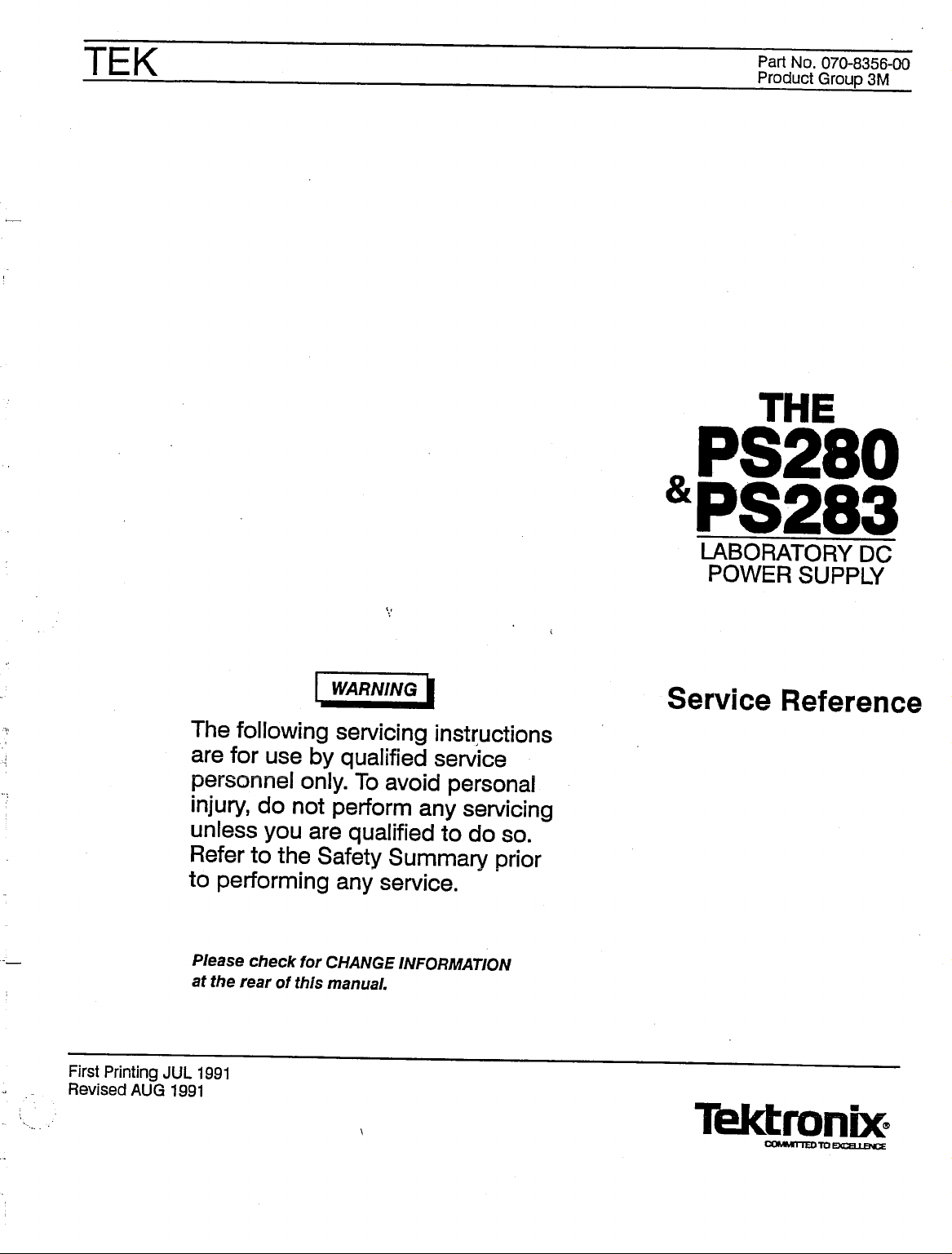
TEK
Part No. 070-8356-00
Product Group 3M
&
PS283
WARNING
The following servicing instructions
are for use by qualified service
personnel only. To avoid personal
injury, do not perform any servicing
unless you are qualified to do so.
Refer to the Safety Summary prior
to performing any service.
Please check for CHANGE INFORMATION
at the rear of this manual.
I
LABORATORY DC
POWER SUPPLY
Service Reference
First Printing JUL 1991
Revised AUG 1991
Tektronix
COMMTTCD
TO
EXEa_LB\CE
Page 2
Copyright©
publication may not be reproduced in any form without the written
permission of Tektronix, Inc.
1991
Tektronix, Inc. All rights
reserved.
Contents of this
Products of
and foreign patents issued and pending.
TEKTRONIX, TEK, SCOPE-MOBILE, and W2S are registered
trademarks of Tektronix, Inc.
Printed in
reserved.
Tektronix,
U.S.A.
Inc., and its subsidiaries are covered by U.S.
Specification and price change privileges are
INSTRUMENT SERIAL NUMBERS
Each instrument
stamped on the chassis. The first two digits designate the country of
manufacture. The last five digits
each instrument. The country of manufacture is identified as follows:
B000000 Tektronix, Inc., Beaverton, Oregon,
E200000 Tektronix United Kingdom, Ltd., Marlow
has a
serial number
of
the serial number are unique
on a
panel insert,
U.S.A.
tag, or
to
G100000 Tektronix Guernsey, Ltd., Channel Islands
HKOOOOO Hong Kong
H700000 Tektronix Holland, NV, Heerenveen,
The Netherlands
JPOOOOO Sony/Tektronix, Japan
TWOOOOO Taiwan
Page 3

WBWtfitiAnnnrinn contents
Specifications
Operating Information
Operators and Service Safety Summary
Symbols and Terms
Specific Precautions
Product Description
General
Specifications
General Operating Instructions
Front Panel
Rear Panel
- -|_i
2-1
The Variable Power Supplies
The Fixed Voltage Power Supply
2-4
xi
xii
1.1
1_2
2-1
2-2
X
2-3
i
Theory
of
Operation
Theory
of
Operation
General
Circuit Description
3.1
Master Voltage Output
Slave Voltage Output
5 V Fixed Voltage Output
3.1
3-1
3-1
3-2
3-4
PS280 & PS283 Laboratory DC Power Supply Module-Level Service Manual
REV AUG 1991
Page 4
Performance Verification
Adjustment
Preparation 4-1
Requirements for Performance 4-1
Warm-up Period 4-1
Access 4-1
Test Equipment 4-1
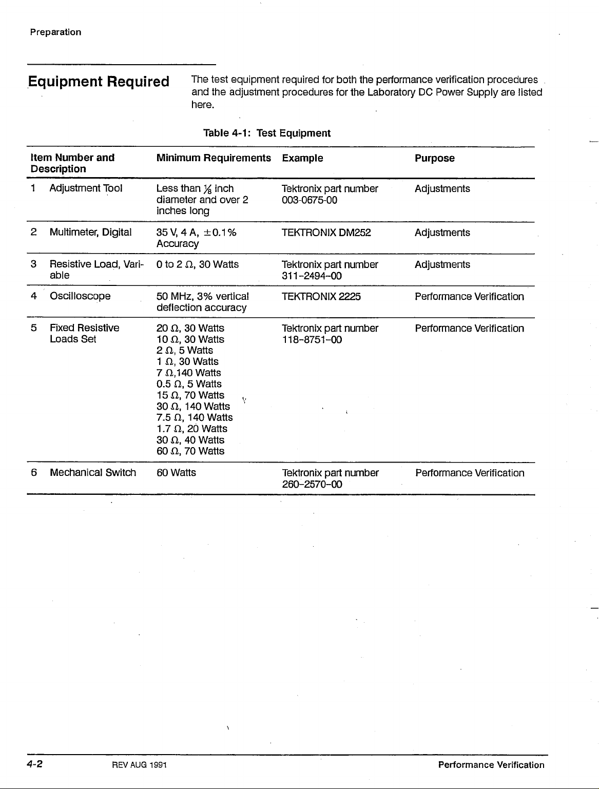
Equipment Required 4-2
Performance Tests 4-3
Constant Current Load Regulation 4-3
Constant Current Ripple and Noise 4-5
Constant Voltage Regulation 4-7
Preparation 5-1
Requirements for Performance 5-1
Personnel 5-1
Warm-up Period 5-1
Access 5-1
Test Equipment 5-1
Maintenance
Adjustment Procedures 5-3
Independent Mode 5-3
Series Tracking Mode . «. 5-5
Parallel Tracking Mode 5-6
5 V Fixed 5-7
Information 6-1
Helpful Procedures 6-1
Preventing ESD 6-1
Inspection and Cleaning 6-5
General Care 6-5
Inspection and Cleaning Procedures 6-5
Inspect Exterior 6-5
Cleaning Procedure - Exterior 6-6
Inspect Interior 6-6
Cleaning Procedure — Interior 6-7
Lubrication 6-8
REV AUG
1991
Contents
Page 5

Options
Removal and Installation Procedures 6-9
Preparation - Please Read 6-9
List of Modules 6-9
General Instructions 6-10
Top Cover Removal 6-10
Slave Circuit Board Removal 6-12
Fuse Circuit Board Removal 6-13
AC Selector Circuit Board Removal 6-14
Master Circuit Board Removal 6-16
Front Panel Display Circuit Boards Assembly Removal 6-17
Front Panel Controls Circuit Board Removal 6-19
Output Connectors Circuit Board Removal 6-21
Power Transistor Circuit Boards Removal 6-23
Options and Accessories 7-1
Power Cord Options 7-1
Standard Accessories 7-1
Optional Accessories 7-1
Parts List
Diagrams
Index
Parts List 8-1
Parts Ordering Information 8-1
Module Replacement 8-1
Using the Parts List 8-2
Item Names 8-2
Indentation System 8-2
Abbreviations 8-2
Diagrams and Circuit Board Illustrations 9.1
Component Values g_1
PS280 & PS283 Laboratory DC Power Supply Module-Level Service Manual
REVAUG 1991
Page 6
WM§$XfX¥\rUlJ List of Illustrations
Figure
2-1:
PS280 or PS283 Front Panel 2-1
Figure 2-2: Variable Power Supply Controls 2-2
Figure 2-3: Fixed Power Supply Controls 2-3
Figure 2-4: PS280 or PS283 Rear Panel 2-4
Figure
3-1:
PS280 or PS283 Variable Outputs Block Diagram 3-3
Figure 3-2: PS280 or PS283 5 V Block Diagram 3-4
Figure
4-1:
Constant Current Test Setup 4-3
Figure 4-2: Constant Current Ripple and Noise Test Setup 4-5
Figure 4-3: Constant Voltage Test Setup 4-7
Figure
5-1:
Master Circuit Board Adjustment Locations 5-8
Figure 5-2: Display Assembly Circuit Board Adjustment Locations ... 5-9
Figure 5-3: Front Panel Controls Circuit Board Adjustment Locations . 5-9
Figure
6-1:
Top Cover Removal 6-11
Figure 6-2: Slave and Fuse Circuit Board Removal 6-13
Figure 6r3: AC Selector and Master Circuit Board Removal 6-15
Figure 6^4: Front Panel Display Assembly Removal 6-18
Figure 6-5: Front Panel Controls Assembly 6-20
Figure 6-6: Output Connectors Circuit Board
and Power Switch Location 6-22
Figure 6-7: Power Transistor Circuit Boards Location 6-23
PS280 & PS283
Laboratory
DC
Power Supply
Figure
8-1:
Exploded View A 8-8
Figure 8-2: Exploded View B 8-16
Module-Level Service Manual REV AUG 1991
vii
Page 7
WMMfflfWinnnnj ust
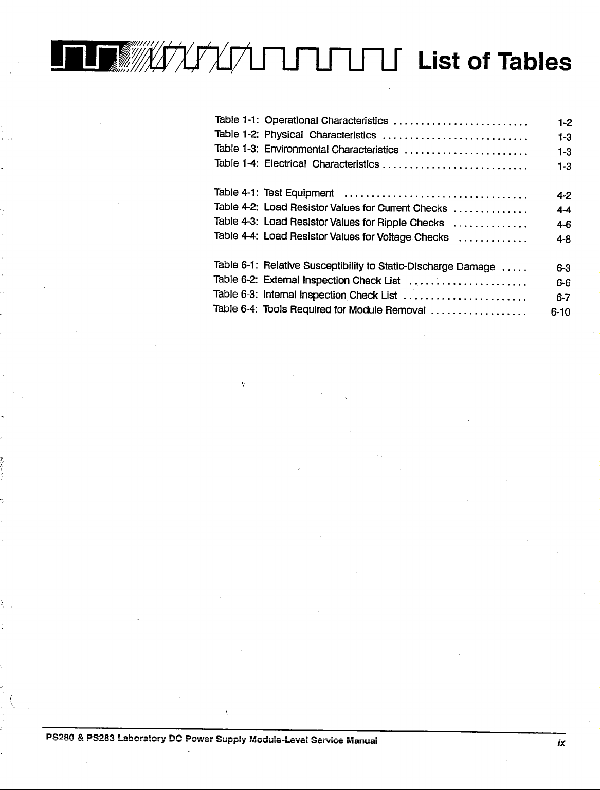
Table 1-1: Operational Characteristics 1-2
Table 1-2: Physical Characteristics 1.3
Table 1-3: Environmental Characteristics 1-3
Table 1-4: Electrical Characteristics 1-3
Table
4-1:
Test Equipment 4-2
Table 4-2: Load Resistor Values for Current Checks 4-4
Table 4-3: Load Resistor Values for Ripple Checks 4-6
Table 4-4: Load Resistor Values for Voltage Checks 4-8
Table
6-1:
Relative Susceptibility to Static-Discharge Damage 6-3
Table 6-2: External Inspection Check List 6-6
Table 6-3: Internal Inspection Check List 6-7
Table 6-4: Tools Required for Module Removal 6-10
of Tables
PS280 & PS2S3 Laboratory DC Power Supply Module-Level Service Manual ;
x
Page 8
Operators and Service Safety Summary
Please take a moment to review these safety precautions. They are provided
for your protection and to prevent damage to the power supply. This safety
information applies to all operators and service personnel.
Symbols and Terms
These two terms
• l^°!L\ statements identify conditions or practices that could result in
damage to the equipment or other property.
ttwwws
•
I
personal injury or loss of life.
These two terms appear on equipment:
•
CAUTION
one reads the marking, or a hazard to property including the equipment
•
DANGER
reads the marking.
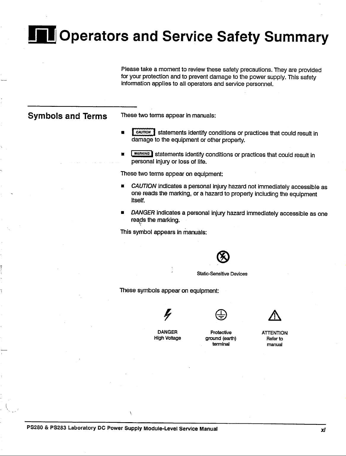
This symbol appears in manuals:
appear
* statements identify conditions or practices that could result in
indicates a personal injury hazard not immediately accessible as
indicates a personal injury hazard immediately accessible as one
in
manuals:
®
Static-Sensitive Devices
These symbols appear on equipment:
DANGER
High Voltage
PS280 & F32S3 Laboratory DC Power Supply Module-Level Service Manual xl
Protective
ground (earth)
terminal
ATTENTION
manual
Page 9
Specific Precautions
Observe all of the following precautions to ensure your personal safety and to
prevent damage to either the PS280 or PS283Laboratory DC Power Supply or
equipment connected to it.
Do Not Perform Service While Alone
Do not perform internal service or adjustment of this product unless another
person capable of rendering first aid and resuscitation is present.
Use Care When Servicing With Power On
Dangerous voltages exist at several points in this product. To avoid personal
injury, do not touch exposed connections or components while power is on.
Disconnect power before removing protective panels, soldering, or replacing
components.
Power Source
The PS280 or PS283 Laboratory DC Power Supply is intended to operate from
a power source that will not apply more than 250 V rms between the supply
conductors or between either supply conductor and ground. A protective
ground connection, through the grounding conductor in the power
essential for safe system operation.
cord,
is
Grounding the power supply
The PS280 or PS283 Laboratory DC Power Supply is grounded through the
power
cord.
To avoid electric shock, plug the power cord into a properly wired
receptacle where earth ground has been verified by a qualified service person.
Do this before making connections to the output terminals of the Laboratory DC
Power Supply. -
Without the protective ground connection, all parts of the PS280 or PS283
Laboratory DC Power Supply are potential shock hazards. This includes knobs
and controls that may appear to be insulators.
Use the Proper Power Cord
Use only the power cord and connector specified for your product. Use only a
power cord that is in good condition.
Use the Proper Fuse
To avoid fire hazard, use only the fuse specified in the parts list for your
uct, and which is identical in type, voltage rating, and current rating.
prod-
REV AUG 1991
Operators and Service Safety Summary
Page 10

Do Not Remove Covers or Panels
To avoid personal injury, do not operate the PS280 or PS283 Laboratory DC
Power Supply without the panels or covers.
Do Not Operate in Explosive Atmospheres
ThePS280 or PS283 Laboratory DC Power Supply provides no explosion
protection from static discharges or arcing components. Do not operate in an
atmosphere of explosive gasses.
PS280 & PS283 Laboratory DC Power Supply Module-Level Service Manual
xll!
Page 11

BmMfJWnr Specifications
Page 12
#%f%M_rLTLn Product Description
This subsection begins with a general description of the PS280 or PS283
Power Supply. The Specifications subsection immediately follows.
General
The Tektronix PS280 or PS283 Laboratory DC Power Supply is a multifunction
bench or portable instrument. This regulated power supply provides a fixed 5 V
output for powering logic circuits and two variable outputs for a wide variety of
test and experimental uses. The PS280 or PS283 can be used in any application where three independent power supplies housed in a single package
represent a convenience.
The PS280 or PS283 contains two identical, independently adjustable DC
power supplies that you can vary from 0 to 30
variable power supplies varies from 0 to 2 A. The current on the PS283
able power supplies varies from 0 to 1 A. In all other respects the instruments
are identical. Unless otherwise noted, descriptions and procedures in this
manual apply to both instruments.
Front panel switches select one of three modes of operation: independent,
series, or parallel. In the independent mode, the output voltage and current of
each supply can be controlled independently. In the two tracking modes, the
variable outputs are connected either in series or in parallel. Under these
circumstances, the controls of the master power supply adjust the voltages or
current of both power supplies. Series mode allows the power supplies to be
varied from 0 to 60 V at 0 to 2 A for the PS280, or 0 to 1 A for the PS283.
Parallel mode allows the power supplies to be varied from 0 to 4 A for the
PS280 at 0 to 30
V,
or from 0 to 2 A at 0 to 30 V for the PS283.
V.
The current on the PS280
vari-
PS280 & PS283 Laboratory DC Power Supply Module-Level Service Manual
REV
AUG 1991
f-f
Page 13
Product Description
Specifications
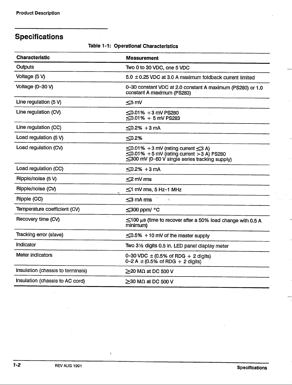
Table 1-1: Operational Characteristics
Characteristic
Outputs
Voltage (5 V)
Voltage (0-30 V)
Line regulation (5 V)
Line regulation (CV)
Line regulation (CC)
Load regulation (5 V)
Load regulation (CV)
Load regulation (CC)
Ripple/noise (5 V)
Ripple/noise (CV)
Ripple (CC)
Measurement
Two 0 to 30
5.0 ±0.25 VDC at 3.0 A maximum foldback current limited
0-30 constant VDC at 2.0 constant A maximum (PS280) or 1.0
constant A maximum (PS283)
<5mV
<0.01%
<0.01%
<0.2%
<0.2%
<0.01 % + 3 mV (rating current <3 A)
<0.01 % +5 mV (rating current >3 A) PS280
<300 mV (0-60 V single series tracking supply)
<0.2%
<2 mV rms
<1 mV
<3 mA rms
VDC,
one 5 VDC
+3mVPS280
+ 5 mV PS283
+3mA
+3mA
rms,
5 Hz-1 MHz
Temperature coefficient (CV)
Recovery time (CV)
Tracking error (slave)
Indicator
Meter indicators
Insulation (chassis to terminals)
Insulation (chassis to AC cord)
<300 ppm/ °C
<100 p.s (time to recover after a 50% load change with 0.5 A
minimum)
<0.5%
-f-10 mV of the master supply
Two 31/2 digits 0.5 in. LED panel display meter
0-30 VDC ±(0.5% of RDG + 2 digits)
0-2 A ±(0.5% of RDG + 2 digits)
>20 MH at DC 500 V
>30 MXl at DC 500 V
REVAUG 1991
Specifications
Page 14
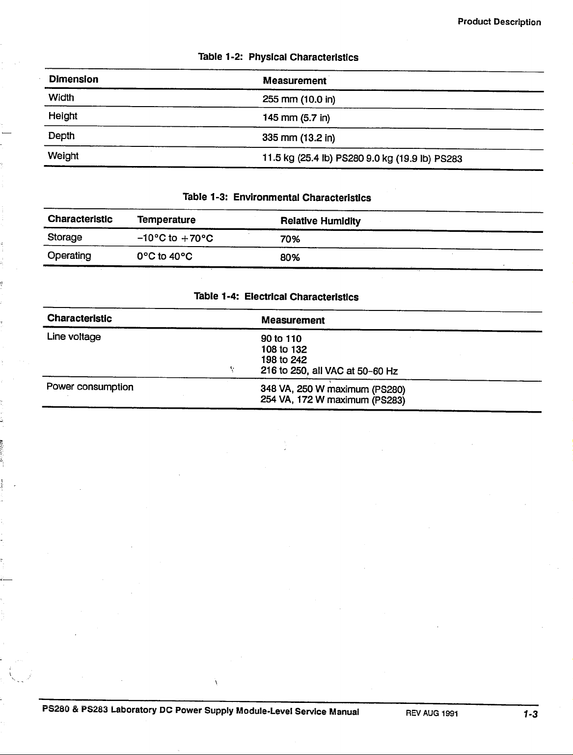
Table 1-2: Physical Characteristics
Product Description
Dimension
Width
Height
Depth
Weight
Characteristic
Storage
Operating
Characteristic
Line voltage
Power consumption
Measurement
255 mm (10.0 in)
145 mm (5.7 in)
335 mm (13.2 in)
11.5 kg (25.4 Ib) PS280 9.0 kg (19.9 Ib) PS283
Table 1-3: Environmental Characteristics
Temperature Relative Humidity
-10°Cto+70°C 70%
0°C to 40 °C 80%
Table 1-4: Electrical Characteristics
Measurement
90 to 110
108 to 132
198 to 242
216 to 250, all VAC at 50-60 Hz
348 VA, 250 W maximum (PS280)
254 VA, 172 W maximum (PS283)
PS2S0 & P5283 Laboratory DC Power Supply Module-Level Service Manual
REV AUG
1991
Page 15
IHF LTOperating Information
Page 16
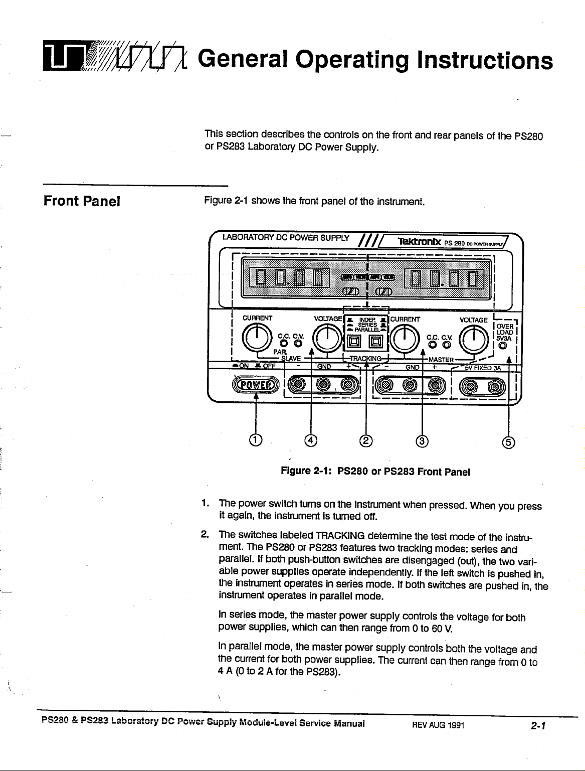
WWXtX General Operating Instructions
Front Panel
This section describes the controls on the front and rear panels of the PS280
or PS283 Laboratory DC Power Supply.
Figure
2-1
shows the front panel of the instrument.
LABORATORY
1.
The power switch turns on the instrument when pressed. When you press
it again, the instrument is turned off.
DC POWER SUPPLY
Figure
2-1:
PS280 or PS283 Front Panel
//// TWCmniX
PS 280
CC POWER
SUPPLY/
2.
The switches labeled TRACKING determine the test mode of the instru-
ment. The PS280 or PS283 features two tracking modes: series and
parallel.
able power supplies operate independently. If the left switch is pushed in,
the instrument operates in series mode. If both switches are pushed in, the
instrument operates in parallel mode.
In series mode, the master power supply controls the voltage for both
power supplies, which can then range from 0 to 60 V.
In parallel mode, the master power supply controls both the voltage and
the current for both power supplies. The current can then range from 0 to
4A(0to2AforthePS283).
PS2S0 & PS283 Laboratory DC Power Supply Module-Level Service Manual
If both push-button switches are disengaged (out), the two
REV AUG
vari-
1991
Page 17

General Operating Instructions
3. These controls affect the right variable power supply. If the instrument is in
a tracking mode, the right power supply is the master. In a tracking mode,
either or both of the control knobs can affect both variable power supplies.
4.
These controls affect the left variable power supply. If the instrument is in a
tracking mode, the left power supply is the slave. In a tracking mode,
either or both of the control knobs have no effect.
5. These controls affect the fixed 5 V power supply.
The Variable Power Supplies
Figure 2-2 shows the controls for the master variable power supply.
CURRENT
VOLTAGE
Figure 2-2: Variable Power Supply Controls
1.
The output terminals for the power supply allow you to plug in the test
leads.
The red one on the right is the positive polarity output terminal. It is
indicated by a + sign above it.
The black one on the left is the negative polarity output terminal. It is
indicated by a - sign above it.
The green one in the middle is the earth and chassis ground.
2.
The voltage control knob allows you to set the output voltage for the
power supply.
REV AUG
1991
3. The current control knob allows you to set the output current for the power
supply.
4.
If the C.V. light is lighted, the power supply is producing a constant volt-
age.
If the C.C. light is lighted, the power supply is producing a constant
current.
Operating Information
Page 18

General Operating Instructions
5. The LED display lights when the instrument is turned on. The numbers
indicate the voltage or current produced by the variable power supply.
6. The AMPS/VOLTS meter selection switch determines whether the LED
display shows the current or the voltage. If the switch is pushed to the left,
the display shows the current. If the switch is pushed to the right, the
display shows the voltage.
The meter selection switch is to the right of the corresponding display for the
slave variable power supply. All other controls are the same for both variable
power supplies.
The Fixed Voltage Power Supply
Figure 2-3 shows the controls for the fixed voltage power supply.
5V FIXED 3A
Figure 2-3: Fixed Power Supply Controls
1.
The output terminals for the power supply allow you to plug in the test
leads.
The red one on the right is the positive polarity output terminal. The
black one on the left is the negative polarity output terminal.
2.
The overload indicator lights when the current on the 5 V power supply
becomes too large.
PS280 & PS2S3 Laboratory DC Power Supply Module-Level Service Manual
REV
AUG 1991
2-3
Page 19

General Operating Instructions
Rear Panel
Figure
2-4
shows the rear panel
of
the instrument.
Figure 2-4: PS280
1.
These two switches allow you
voltage. Push the top switch
100
to
120
V;
push
it to
the right
•gggss
1
^
S
TEOTRONKINC,
BEAVEHTON.,OH,U.SA
1UKXTAIWAMJI.0.C
or
PS283 Rear Panel
to
set the instrument for the correct line
to
the left
if
the line voltage
If
the line voltage
is in
^
A©
s
is in
the range
y
the range
of
220
of
to
The bottom switch determines whether the line voltage
high end
the low end
voltage
2.
This
holder to ensure that you are using the correct fuse. This
change the fuse.
3. This
of
the voltage range. Push
of
the range-100
is at
the high end
is
the fuse holder. Pull the middle tab down and out
is
the receptacle for the power
of
the
or
220
range
it to
V;
-120
cord.
the left
push
or
it to
is
In the low or the
if
your line voltage
the right
240 V.
if
to
open the fuse
is
also how you
is at
your line
Operating Information
Page 20
BBSftXfTTheory of Operation
Page 21
WMSPXfXVtTirL
Theory
of Operation
General
Circuit Description
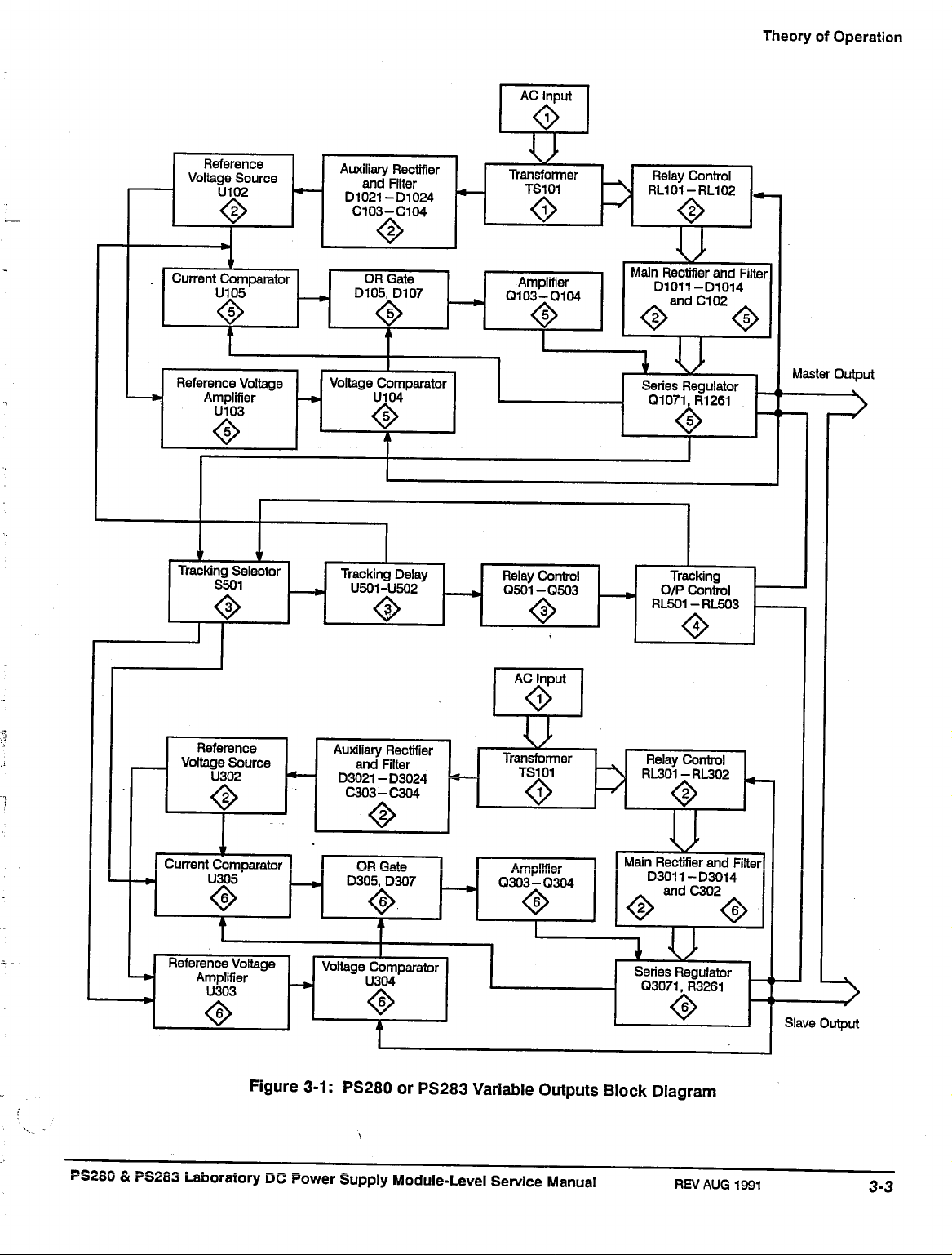
The PS280 or PS283 Laboratory DC Power Supply consists of two variable
output supplies and one 5 V fixed output. The circuit elements and their func-
tions are described in the Circuit Description, using the Block Diagram as an
aid in following the circuit description.
The detailed circuit description uses the block diagram, Figure
for the circuit description. The Block Diagram contains both the circuit component reference designators and lists the appropriate schematic on which they
can be found.
3-1
as a guide
Master Voltage Output
Single phase input power is applied to transformer
The outputs from transformer
relays
RL101
required from the Series Regulator by providing varying voltages to the Main
Rectifier circuit, depending on the output requirements.
The Main Rectifier circuit consists of diodes D1011 through D1014 that form a
full wave bridge rectifier. The output from the bridge rectifier is filtered by
capacitor
circuit.
and RL102. The relay control circuit limits the power dissipation
C102.
The filtered output voltage is applied to the Series Regulator
TS101
are applied to the Main Rectifier circuit by
TS101
through the AC input
The Series Regulator circuit consists mainly of
a regulated voltage to the Laboratory DC Power Supply Master output.
The Auxiliary Rectifier circuit consists of diodes 01021 through D1024 that
form a full wave bridge rectifier. The bias voltage from the bridge rectifier is
filtered by capacitors C103 and C104. This bias voltage is then applied to the
Reference Voltage circuit.
The Reference Voltage circuit consists of
ence circuit provides a regulated +15 V and -15 V to be used by the Current
Comparator circuit and the Reference Voltage Amplifier circuit.
The Current Comparator circuit, consisting of U105, limits the output current of
the Series Regulator circuit through OR gate and Amplifier circuit consisting of
D107,
and Q103 and Q104. Master CURRENT control, VR105, sets the maxi-
mum output current level.
P3280 & PS263 Laboratory DC Power Supply Module-Level Service Manual
U101,
Q1071
Q101,
REV AUG
and
R1261,
and Q102. This Refer-
1991
that deliver
Page 22

Theory of Operation
The Reference Voltage Amplifier circuit consists mainly of U103, and the
Voltage Comparator circuit consists mainly of U104. U104 compares the
voltage from the Reference Voltage Amplifier with feedback from the output
voltage and, through diode D105 and the amplifier circuit of Q103 and Q104,
provides a calibrated output voltage.
The Tracking Selector switches (S501A and S501B), along with the Tracking
Delay circuit (U501 and U502), Relay Control circuit
and the Tracking Relays
(RL501,
RL502, and RL503) set the configuration of
(Q501,
Q502, and Q503),
the Master and Slave outputs.
The TRACKING Mode Switches set the Laboratory DC Power Supply in one of
three modes: INDEPendent Mode, SERIES tracking mode, or PARALLEL
mode.
The on/off conditions of relays
RL501,
RL502, and RL503 are shown
below, according to the operating mode selected.
Tracking Operation
Series Tracking
Parallel Tracking
Independent O/P
Off
On
Off
On
On
Off
Off
On
Off
When in the SERIES Tracking mode, The Master negative output is shorted to
the Slave positive output. Also, the Master output voltage provides the voltage
reference for the Reference Voltage Amplifier circuit, U303.
When in the PARALLEL Tracking mode, both the negative and positive outputs
from the Master outputs are shorted to the negative and positive outputs of the
Slave outputs. A reference voltage for Current Comparator U305 is provided
through R1261 from the Master supply circuit.
U501 and U502 are used to protect the Laboratory DC Power Supply from
instant high voltage/current during the switching time of the relay contacts.
Slave Voltage Output
The Slave output circuitry performs the same as described for the Master
Voltage output. The circuits are the same except for the component names.
Refer to the block diagram for appropriate component names of the Slave
output circuit.
REV
3-2
AUG1991
Theory of Operation
Page 23
AC Input
Theory
of
Operation
Reference
Voltage Source
<2>
Current Comparator
Reference Voltage
Amplifier
Tracking Selector
Auxiliary Rectifier
and Filter
D1021-D1024
C103-C104
D105,
D107
Voltage Comparator
Tracking Delay
U501-U502
u
Transformer
O
Amplifier
Q103-Q104
Relay Control
Q501-Q503
Relay Control
RL101-RL102
JJ
Main Rectifier and Filter
D1011-D1014
u
Series Regulator
Q1071.R1261
Tracking
O/P Control
RL501-RL503
Master Output
Reference
Voltage Source
Current Comparator
Reference Voltage
Amplifier
Figure
Auxiliary Rectifier
and Filter
D3021-D3024
C303-C304
Main Rectifier and Filter
0302.
D307
Amplifier
Q303-Q304
'
A """"A
Voltage Comparator
3-1:
PS280 or PS283 Variable Outputs Block Diagram
3_JJ.
<3>
Relay Control
RL301-RL302
u
D3011-D3014
Series Regulator
Q3071.
R3261
Slave Output
P3280 & PS283 Laboratory
uu
power supply Module-Level Service Manual
REV
AUG
1991
Page 24

Theory of Operation
5 V Fixed Voltage Output
AC Input
u\
Transformer
•
Current Comparator
The 12 V output from transformer
The Rectifier circuit consists of diodes D4011 through D4014 that form a full
wave bridge rectifier. The output from the bridge rectifier is filtered by capacitor
C401.
The filtered output voltage is applied to the Series Regulator circuit.
The Series Regulator circuit consists mainly of Q402 and R407, that deliver a
regulated voltage to the Laboratory DC Power Supply 5 V Fixed output.
The Current Comparator circuit, consisting of
the Series Regulator circuit through Q401.
Rectifier and Filter
D4011-D4014
<>
Series Regulator
andC401
Q402,
R407
TS101
is applied to the Rectifier circuit.
U401,
limits the output current of
5 V Fixed
Output
>
<2>
Figure 3-2: PS280 or PS283 5 V Block Diagram
REVAUG 1991
Theory of Operation
Page 25

SIB Performance Verification
Page 26
WMiMrWinnnnTL Preparation
Purpose - Use this procedure to verify that the Laboratory DC Power Supply
is in conformance with its specifications as listed in Section 1, Specifications.
It can also be used for incoming inspection of the Laboratory DC Power
Supply.
Performance Verification Interval
performed whenever the accuracy or functions of the power supply are
question.
performing the adjustments in Section 5, Adjustments.
Requirements
Performance address the following requirements.
for
Before you perform these performance verification procedures, you need to
Warm-up Period
The Laboratory DC Power Supply requires a 20 minute warm-up time in
20°C to 30°C environment before a performance verification
A performance verification should be used to verify the need for
Access
Cabinet removal is not required to perform any of these procedures
Test Equipment
Table
4-1
lists all the test equipment required to perform both the Performance
Verification procedures and the Adjustment Procedures for the PS280
Laboratory DC Power Supply.
-A
performance verification should be
is
made.
in
a
or
PS283
PS2S0 & P32S3 Laboratory DC rower supply Module-Level Service Manual
REV
AUG 1991
4.7
Page 27
Preparation
Equipment Required
Item Number and
Description
1 Adjustment Tool
2 Multimeter, Digital
3 Resistive Load,
Vari-
4 Oscilloscope
5 Fixed Resistive
Loads Set
Minimum Requirements
Less than % inch
diameter and over 2
inches long
35
Accuracy
0 to 2 n, 30 Watts
50 MHz, 3% vertical
deflection accuracy
20 a, 30 Watts
10 a, 30 Watts
2 fl, 5 Watts
1 a, 30 Watts
7 a, 140 Watts
0.5 a, 5 Watts
15X1,70 Watts
30 a, 140 Watts
7.511,140
1.7 n, 20 Watts
30 a, 40 Watts
60 a, 70 Watts
The test equipment required for both the performance verification procedures
and the adjustment procedures for the Laboratory DC Power Supply are listed
Table
4-1:
Test
Equipment
Example
Tektronix part number
Purpose
Adjustments
003-0675-00
V,
4 A, ±0.1%
TEKTRONIX DM252
Tektronix part number
Adjustments
Adjustments
311-2494-00
TEKTRONIX 2225
Tektronix part number
Performance Verification
Performance Verification
118-8751-00
Watts
6 Mechanical Switch 60 Watts
REV
AUG
1991
Tektronix part number
260-2570-00
Performance Verification
Performance Verification
Page 28

WMMPXfXlftnnr
Performance Tests
Constant Current
Load Regulation
Equipment Required: Digital multimeter and load resistors
Figure
4-1:
Constant Current Test Setup
1.
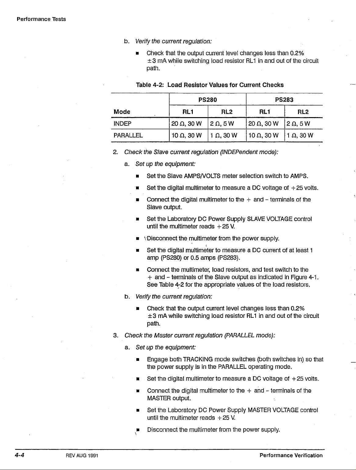
Check the Master current regulation
a. Set up the equipment:
• Disengage both TRACKING mode switches (both switches out) so
that the power supply is in the INDEPendent operating mode.
(INDEPendent
mode):
•*-i
RL1
• Set the Master AMPS/VOLTS meter selection switch to AMPS.
• Set the digital multimeter to measure a DC voltage of +
• Connect the digital multimeter to the + and - terminals of the
MASTER output.
• Set the Laboratory DC Power Supply MASTER VOLTAGE control
until the multimeter reads +25 V.
• Disconnect the multimeter from the power supply.
• Set the digital multimeter to measure a DC current of at least 1
amp (PS280) or 0.5 amps (PS283).
• Connect the multimeter, load resistors, and test switch to the
+ and - terminals of the Master output as indicated in Figure
See Table 4-2 for the appropriate values of the load resistors.
PS280 & PS283 Laboratory DC Power Supply Module-Level Service Manual
REV AUG
1991
25
volts.
4-1.
Page 29
Performance Tests
b.
Verify
the current regulation:
• Check that the output current level changes less than 0.2%
±3 mA while switching load resistor
Table 4-2: Load Resistor Values for Current Checks
RL1
in and out of the circuit
PS280
oae
M
INDEP
PARALLEL
2.
Check the Slave current regulation
a. Set up the equipment:
• Set the Slave AMPS/VOLTS meter selection switch to AMPS.
• Set the digital multimeter to measure a DC voltage of + 25 volts.
• Connect the digital multimeter to the + and - terminals of the
Slave output.
• Set the Laboratory DC Power Supply SLAVE VOLTAGE control
until the multimeter reads +25 V.
• 'Disconnect the multimeter from the power supply.
• Set the digital multimeter to measure a DC current of at least 1
amp (PS280) or 0.5 amps (PS283).
a Connect the multimeter, load resistors, and test switch to the
+ and - terminals of the Slave output as indicated in Figure
See Table 4^2 for the appropriate values of the load resistors.
RL1
20
D.,
30
10 a, 30
W
w
RL2
,5W
2O
,30W
in
(INDEPendent
20
10
RL1
a 30
a
so
mode):
PS283
W
w
RL2
2fl.5W
1
a
30
w
4-1.
REV AUG
1991
b.
Verify
3. Check the Master current regulation
a. Set up the equipment:
the current regulation:
• Check that the output current level changes less than 0.2%
±3 mA while switching load resistor
• Engage both TRACKING mode switches (both switches in) so that
the power supply is in the PARALLEL operating mode.
• Set the digital multimeter to measure a DC voltage of +
• Connect the digital multimeter to the + and - terminals of the
MASTER output.
• Set the Laboratory DC Power Supply MASTER VOLTAGE control
until the multimeter reads +25 V.
• Disconnect the multimeter from the power supply.
RL1
(PARALLEL
in and out of the circuit
mode):
25
volts.
Performance Verification
Page 30

Performance Tests
• Set the digital multimeter to measure a DC current of at least
1 amp (PS280) or 0.5 amps (PS283).
• Connect the multimeter, load resistors, and test switch to the
+ and - terminals of the Master output as indicated in Figure
See Table 4-2 for the appropriate values of the load resistors.
b.
Verify
the current regulation:
• Check that the output current level changes less than 0.2%
±5 mA while switching load resistor
RL1
in and out of the circuit
4-1.
Constant Current
Ripple and Noise
Equipment Required: Oscilloscope and load resistors
Figure 4-2: Constant Current Ripple and Noise Test Setup
1.
Check the Master current ripple:
a. Set up the equipment:
• Disengage both TRACKING mode switches (both switches out) so
that the power supply is in the INDEPendent operating mode.
• Set the Master AMPS/VOLTS meter selection switch to VOLTS.
• Set the Laboratory DC Power Supply to+25 volts (using the
digital display).
• Connect the test oscilloscope and load resistors to the + and terminals of the Master output as indicated in Figure 4-2. See
Table 4-3 for the appropriate values of the load resistors.
b.
Verify
PS280 & PS283 Laboratory DC Power Supply Module-Level Service Manual
the current ripple:
• Check that the peak-to-peak ripple viewed with the test oscilloscope is less than 2.5 mV.
REV AUG 1991
Page 31

Performance Tests
c. Set up the
• Engage both TRACKING mode switches (both switches in) so that
d.
Verify
• Check that the peak-to-peak ripple viewed with the test oscillo-
e. Set up the
• Disengage the right TRACKING mode switch (switch out) so that
f.
Verify
• Check that the peak-to-peak ripple viewed with the test oscillo-
Table 4-3: Load Resistor Values for Ripple Checks
Mo,e
INDEP
equipment:
the power supply is in the PARALLEL operating mode.
the current ripple:
scope is less than 2.5 mV.
equipment:
the power supply is in the SERIES operating mode.
the current ripple:
scope is less than 5 mV.
15n,
RL
70W
PS280
0.5 n, 5 W
Rs
30
n, 40
PS283
RL
W
Rs
0.5 n,5W
PARALLEL
2.
Check the Slave current ripple:
7 a 140 W
a. Set up the equipment:
• Disengage both TRACKING mode switches (both switches out) so
that the power supply is in the INDEPendent operating mode.
• Set the Slave AMPS/VOLTS meter selection switch to VOLTS.
• Set the Laboratory DC Power Supply to +
digital display).
• Connect the test oscilloscope and load resistors to the + and -
terminals of the Slave output as indicated in Figure 4-2. See Table
4-3 for the appropriate values of the load resistors.
b.
Verify
the current ripple:
• Check that the peak-to-peak ripple viewed with the test oscilloscope is less than 2.5 mV.
10n,
30w
15
a,70
25
volts (using the
W
0.5 fl,5W
REV AUG
1991
Performance Verification
Page 32

Performance Tests
Constant Voltage
Regulation
Equipment Required: Digital multimeter and load resistors
Figure 4-3: Constant Voltage Test Setup
1.
Check the Master voltage regulation:
a. Set up the equipment:
• Disengage both TRACKING mode switches (both switches out) so
that the power supply is in the INDEPendent operating mode.
v
• Set the digital multimeter to measure a DC voltage of + 60 volts.
• Connect the digital multimeter and load resistors to the + and terminals of the Master output as indicated in Figure 4-3. See
Table 4-4 for the appropriate values of the load resistor.
b.
Verify
c. Set up the equipment:
d.
Verify
e. Set up the equipment:
the voltage output range:
• Check that the Laboratory DC Power Supply can be adjusted from
0 to 30 V.
• Engage the left TRACKING mode switch (switch in) and disengage the right TRACKING mode switch (switch out) so that the
power supply is in the SERIES operating mode.
the voltage output range:
• Check that the Laboratory DC Power Supply can be adjusted from
0 to 60 V.
• Engage both TRACKING mode switches (both switches in) so that
the power supply is in the PARALLEL operating mode.
PS280 & PS283 Laboratory DC Power Supply Module-Level Service Manual
REV AUG
1991
Page 33

Performance Tests
f.
Verify
the voltage output range:
• Check that the Laboratory DC Power Supply can be adjusted from
0 to 30 V.
Table 4-4: Load Resistor Values for Voltage Checks
INDEP
SERIES
PARALLEL
5 V Fixed
2. Check the Slave voltage regulation:
a. Set up the equipment:
• Disengage both TRACKING mode switches (both switches out) so
that the power supply is in the INDEPendent operating mode.
• Set the digital multimeter to measure a DC voltage of +
• Connect the digital multimeter and load resistors to the + and terminals of the Slave output as indicated in Figure 4-3. See Table
•4-4
for the appropriate values of the load resistor.
b.
Verify
the voltage output range:
• Check that the Laboratory DC Power Supply can be adjusted from
0 to 30 V.
15 n,
30
a
7.5 n,
1.7 n,
PS280
RL
70 W
140 W
140 W
20 W
PS283
RL
30 n, 40 W
60 a, 70 W
15n, 70W
1.7 n, 20 W
30
volts.
REVAUG 1991
3. Check the 5 V Fixed voltage regulation:
a. Set up the equipment:
• Set the digital multimeter to measure a DC voltage of +5 volts.
• Connect the digital multimeter and load resistors to the 5 V FIXED
terminals. Use the test setup illustrated in Figure 4-3 and see
Table 4-4 for the appropriate values of the load resistor.
b.
Verify
the voltage output range:
• Check that the Laboratory DC Power Supply maintains an output
of5V, ± 0.25 V.
Performance Verification
Page 34

WKSWXiAnnns Adjustment
Page 35
WKSffiyWUinnnni Preparation
Requirements
Performance
This section contains information needed
Supply.
Description - The
• This general information about adjusting
• Written procedures
Purpose — This procedure
mance with
be used
Adjustment Interval - As a
performed every 2000 hours
for
ments
Before you perform this procedure, you need
Personnel
Adjustment Procedures
for
manually adjusting
is
its
specifications
to
optimize the performance
as
of
to
adjust your Laboratory DC Power
are
divided into
the
power supply.
the
power supply.
used
to
return
the
power supply
listed
in
Section 1, Specifications.
of
the power supply.
general rule, these adjustments should
operation
or
once a year
to
address the following require-
two
parts:
to
confor-
It
if
used infrequently.
can also
be
This procedure
is
only
to be
performed
by
trained service technicians.
Warm-up Period
This power supply requires a 20 minute warm-up time
environment before performing this adjustment procedure. Adjustments
formed before the operating temperature
adjustment.
has
stabilized may cause errors
in a
20°C
to
30°C
Access
Removal
Maintenance Section
of
the cover
is
required
for
instructions
to
adjust this power supply. Refer
on
how
to
remove the cover.
to the
Test Equipment
The test equipment required
Power Supply
is
listed in Table
to
adjust the PS280
4-1
on
page
4-2.
or
PS283 Laboratory
per-
in
DC
PS280 & PS283 Laboratory
DC
Power Supply Module-Level Service Manual
REV
AUG 1991
5-f
Page 36

BK#%T%|7tr Adjustment Procedures
Independent Mode Equipment
See Figures 5-1 and 5-2 on pages 5-8 and 5-9 for adjustment locations used
in this procedure.
1.
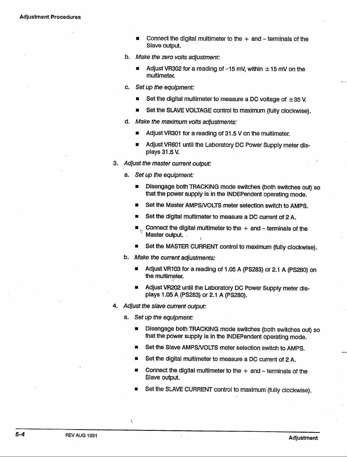
Adjust the master voltage output:
a. Set up the equipment:
• Disengage both TRACKING mode switches {both switches out) so
• Set the Master AMPS/VOLTS meter selection switch to VOLTS.
• Set the digital multimeter to measure a DC voltage of ±16 mV.
• Set the Laboratory DC Power Supply MASTER VOLTAGE control
• Connect the digital multimeter to the + and - terminals of the
b.,, Make the zero volts adjustment:
• Adjust VR102 for a reading of-15 mV, within ± 15 mV on the
c. Set up the equipment:
Required:
that the power supply is in the INDEPendent operating mode.
to minimum (fully counterclockwise).
Master output.
multimeter.
Digital multimeter
• Set the digital multimeter to measure a DC voltage of ± 35 v.
• Set the MASTER VOLTAGE control to maximum (fully clockwise).
d.
Make the maximum volts adjustments:
• Adjust VR101 for a reading of 31.5 V on the multimeter.
• Adjust VR201 until the Laboratory DC Power Supply meter displays 31.5 V.
2.
Adjust the slave voltage output:
a. Set up the equipment:
• Disengage both TRACKING mode switches (both switches out) so
that the power supply is in the INDEPendent operating mode.
• Set the Slave AMPS/VOLTS meter selection switch to VOLTS.
• Set the digital multimeter to measure a DC voltage of ±16 mV.
• Set the Laboratory DC Power Supply SLAVE VOLTAGE control to
minimum (fully counterclockwise).
PS280 & PS283 Laboratory DC Power Supply Module-Level Service Manual
REV
AUG 1991
5.3
Page 37
Adjustment Procedures
• Connect the digital multimeter to the + and - terminals of the
Slave output.
b. Make the zero volts adjustment:
• Adjust VR302 for a reading of-15 mV, within ± 15 mV on the
multimeter.
c. Set up the equipment:
• Set the digital multimeter to measure a DC voltage of ± 35 V.
• Set the SLAVE VOLTAGE control to maximum (fully clockwise).
d.
Make the maximum volts adjustments:
• Adjust
• Adjust
VR301
VR601
for a reading of 31.5 V on the multimeter.
until the Laboratory DC Power Supply meter dis-
plays 31.5V.
3. Adjust the master current output:
a. Set up the equipment:
• Disengage both TRACKING mode switches (both switches out) so
that the power supply is in the INDEPendent operating mode.
• Set the Master AMPS/VOLTS meter selection switch to AMPS.
• Set the digital multimeter to measure a DC current of 2 A.
•, Connect the digital multimeter to the + and - terminals of the
Master output. .
• Set the MASTER CURRENT control to maximum (fully clockwise).
b. Make the current adjustments:
• Adjust VR103 for a reading of 1.05 A (PS283) or
the multimeter.
• Adjust VR202 until the Laboratory DC Power Supply meter dis-
plays 1.05 A (PS283) or
2.1
A (PS280).
2.1
A (PS280) on
5-4
REV AUG1991
4.
Adjust the slave current output:
a. Set up the equipment:
• Disengage both TRACKING mode switches (both switches out) so
that the power supply is in the INDEPendent operating mode.
• Set the Slave AMPS/VOLTS meter selection switch to AMPS.
• Set the digital multimeter to measure a DC current of 2 A.
• Connect the digital multimeter to the + and - terminals of the
Slave output.
• Set the SLAVE CURRENT control to maximum (fully clockwise).
Adjustment
Page 38

b. Make the current adjustments:
Adjustment Procedures
Series Tracking
Mode
• Adjust VR303 for a reading of 1.05 A (PS283) or
the multimeter.
• Adjust VR602 until the Laboratory DC Power Supply meter displays 1.05 A (PS283) or
Disconnect the test setup.
Equipment Required: Digital multimeter
See Figures
in this procedure.
1.
Adjust the series tracking Mode:
a. Set up the equipment:
5-1
and 5-3 on pages 5-8 and 5-9 for adjustment locations used
• Engage the left TRACKING mode switch (switch in) and disengage the right TRACKING mode switch (switch out) so that the
power supply is in the SERIES operating mode.
• Set the SLAVE CURRENT control to midrange.
• Set the MASTER VOLTAGE control to minimum (fully
counterclockwise).
2.1
A (PS280).
2.1
A (PS280) on
«. • Set the digital multimeter to measure a DC voltage of ±16 mV.
• Connect the digital multimeter to the + and - terminals of the
Master output and note the reading obtained.
• Connect the digital multimeter to the + and - terminals of the
Slave output.
b. Make the zero voltage tracking adjustment:
• Adjust VR306 until the voltage output of the SLAVE output matches
the reading obtained from the MASTER output.
c. Set up the equipment:
• Set the MASTER VOLTAGE control to maximum (fully clockwise).
• Set the digital multimeter to measure a DC voltage of ± 35 V.
• Connect the digital multimeter to the + and - terminals of the
Master output and note the reading obtained.
• Connect the digital multimeter to the + and - terminals of the
Slave output.
PS280 & PS283 Laboratory DC Power Supply Module-Level Service Manual
REV AUG
1991
Page 39

Adjustment Procedures
d.
Make the maximum voltage tracking adjustment:
• Adjust
Recheck the value of the Master output compared to the value of
the Slave output. Readjust
Disconnect the test setup.
Parallel Tracking Equipment
ModG See Figure
1.
Adjust the parallel tracking Mode:
a. Set up the
• Disengage both TRACKING mode switches (both switches out) so
• Set the MASTER VOLTAGE and CURRENT controls to minimum
VR501
the reading obtained from the Master output.
until the voltage output of the Slave output matches
wore
VR501
Required:
5-1
on page 5-8 for adjustment locations used in this procedure.
that the power supply is in the INDEPendent operating mode.
(fully counterclockwise).
Digital multimeter
equipment:
if the outputs do not match.
• v Set the digital multimeter to measure a DC current of 4 A.
• Connect the digital multimeter to the + and - terminals of the
Master output.
• Set the MASTER VOLTAGE control to midrange and adjust the
MASTER CURRENT control until a reading of 1 A (PS283) or 2 A
(PS280) is displayed on the multimeter.
NOTE
Do not readjust the
of this procedure.
• Engage both TRACKING switches (both switches in) so that the
power supply is in the PARALLEL operating mode.
• Set the SLAVE CURRENT control to maximum (fully clockwise)
and set the SLAVE VOLTAGE control to midrange.
b. Make the parallel tracking adjustment:
• Adjust VR502 until a reading of 2 A (PS283) or 4 A (PS280) is
displayed on the multimeter.
CURRENT
control setting through the remainder
5-6
REV AUG1991
Disconnect the test setup.
Adjustment
Page 40
5 V
Fixed Equipment
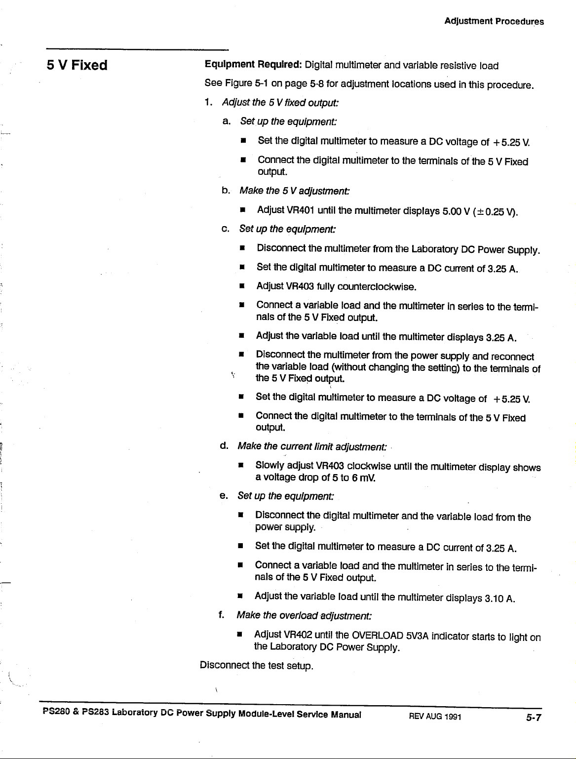
See Figure 5-1 on page 5-8 for adjustment locations used in this procedure.
1.
Adjustment Procedures
Required:
Adjust the 5 V fixed output:
a. Setup the equipment:
• Set the digital multimeter to measure a DC voltage of + 5.25 V.
• Connect the digital multimeter to the terminals of the 5 V Fixed
output.
b. Make the 5 V adjustment:
Digital multimeter
and
variable resistive load
• Adjust
c. Set up the equipment:
• Disconnect the multimeter from the Laboratory DC Power Supply.
• Set the digital multimeter to measure a DC current of 3.25 A.
• Adjust VR403 fully counterclockwise.
• Connect a variable load and the multimeter in series to the termi-
• Adjust the variable load until the multimeter displays 3.25 A.
• Disconnect the multimeter from the power supply and reconnect
the 5 V Fixed output.
• Set the digital multimeter to measure a DC voltage of + 5.25 V.
• Connect the digital multimeter to the terminals of the 5 V Fixed
d.
Make the current limit adjustment:
• Slowly adjust VR403 clockwise until the multimeter display shows
a voltage drop of 5 to 6 mV.
e. Set up the equipment:
VR401
nals of the 5 V Fixed output.
the variable load (without changing the setting) to the terminals of
output.
until the multimeter displays 5.00 V (± 0.25 V).
• Disconnect the digital multimeter and the variable load from the
power supply.
• Set the digital multimeter to measure a DC current of 3.25 A.
• Connect a variable load and the multimeter in series to the terminals of the 5 V Fixed output.
• Adjust the variable load until the multimeter displays 3.10 A.
f. Make the overload adjustment:
• Adjust VR402 until the OVERLOAD 5V3A indicator starts to light on
the Laboratory DC Power Supply.
Disconnect the test setup.
P32S0 & PS2S3 Laboratory DC Power Supply Module-Level Service Manual
REV
AUG 1991
5.7
Page 41

Adjustment Procedures
Master
Maximum
Master
Maximum
a'iiliM!!
O
O^
-• 8 = ~
0 I Ill+lfl
oo
+
Master
Minimum
Parallel
5 V Overload
Mi+0+riiJS^
VR303 VR301 VR306 VR302
Slave Slave Serial Slave
Maximum Maximum Minimum Volts Minimum
Amps Volts Volts
Figure
5-1:
Master Circuit Board Adjustment Locations
5V Amps
REV AUG
1991
Adjustment
Page 42

Adjustment Procedures
| J2021 | | J2041
1 1
T
T
-\-
Display Maximum Maximum
Voltage Amps Amps
Tracking
Voltage
J207 J205
L
J20B^-^J206
nup
11
o
1 ^111
1 1
-
t
'
\\\\
VR601 VR602 VR202
Slave Slave Master
Figure 5-2: Display Assembly Circuit Board Adjustment Locations
T T
I T ^r
o
+
L
/-O
Display
Voltage
U
* oo • *r
Figure 5-3: Front Panel Controls Circuit Board Adjustment Locations
1
1
1
1
u-ir-
1
^
PS280 & PS283 Laboratory DC Power Supply Module-Level Service Manual
5-9
Page 43

#%F%M_n_nj Maintenance
Page 44
IHBllWXFlnnnJirL Information
Helpful Procedures
This section contains the information
nance on the Laboratory DC Power Supply. This section of the manual contains information on static-sensitive components, preventive maintenance,
removal and installation procedures.
The following sections contain information/procedures that may be related
doing maintenance.
• Section 2, Operating Information, covers instructions useful when operating the oscilloscope in order to troubleshoot it.
strategy and lists options for obtaining maintenance service and for replacing failed modules.
• Section 3, Theory
ule,
or block level.
• Section 4, Performance Verification, contains procedures that may
useful
in
isolating problems to modules by testing power supply perform-
• Section 5, Adjustment Procedures, addresses after repair adjustment and
thevinterval between periodic adjustments.
adjusting the internal circuits of this power supply.
of
Operation, contains a circuit description at the mod-
to do
periodic and corrective mainte-
It
also details the service
It
contains a procedure for
and
to
be
Preventing ESD
• Section 9, Diagrams, contains the schematics of the individual circuit
boards.
• Section 8, Replaceable
number and contains the exploded views of the power supply.
The following precautions apply when performing any maintenance involving
internal access to the instrument.
Static discharge can damage any semiconductor component in this
instrument.
This instrument contains electrical components that are susceptible to damage from static discharge. Table 6-1 lists the relative susceptibility of various
classes
unprotected environments.
of
semiconductors. Static voltages
Parts,
lists all field replaceable modules by part
of 1 kV to 30 kV are common
in
PS28Q & PS2S3 Laboratory DC Power Supply Module-Level Service Manual
REV AUG
1991
6-1
Page 45

Information
When performing maintenance, observe the following precautions to avoid
component damage:
1.
Minimize handling of static-sensitive components.
2.
Transport and store static-sensitive components or assemblies in their
original containers or on a metal
static-sensitive components or modules.
3. Discharge the static voltage from your body by wearing a grounded
antistatic wrist strap while handling these components. Servicing staticsensitive components or assemblies should be performed only at a
static-free work station by qualified service personnel.
4.
Nothing capable of generating or holding a static charge off the work
station surface.
5. Keep the component leads shorted together whenever possible.
6. Pick up components or modules by their bodies, never by their leads.
7. Do not slide the components or modules over any surface.
8. Avoid handling components or modules in areas that have a floor or
work-surface covering capable of generating a static charge.
rail.
Label any package that contains
9. Use a soldering iron that is connected to earth ground.
10.
Use only approved antistatic, vacuum-type desoldering tools for compo-
nent removal.
G-2 Maintenance
Page 46

Table
6-1:
Relative Susceptibility to Static-discharge Damage
Information
Semiconductor Classes
MOS or CMOS microcircuits or discretes, or linear
microcircuits with MOS inputs (Most Sensitive)
ECL
Schottky signal diodes
Schottky TTL
High-frequency bipolar transistors
JFET
Linear microcircuits
Low-power Schottky TTL
TTL (Least Sensitive)
1
Voltage equivalent for levels (voltage discharged from a 100 pF capacitor through resis-
tance of 100 fl):
1 =
100
to 500 V 6 =
2 = 200 to 500 V 7 =
3 = 250 V 8 =
4 = 500 V 9 = 1200
5 = 400 to 600
V
600
400
900 V
to
800 V
to
1000 V
V
(est)
Relative
Susceptibility
Levels
1
1
2
3
4
5
6
7
8
9
PS280 & PS283 Laboratory DC Power Supply Module-Level Service Manual REVAUG 1991
Page 47

WMMPXlWU~ Inspection and Cleaning
Inspection and Cleaning describes how to inspect for dirt and damage on,
and how to clean the exterior and interior of, the Laboratory DC Power Supply.
Such inspection and cleaning are performed as preventative maintenance.
Preventive maintenance, when performed regularly, may prevent instrument
malfunction and enhance reliability.
Preventive maintenance consists of visually inspecting and cleaning the power
supply and using general care when operating it.
The severity of the environment in which the power supply is used determines
the required frequency of maintenance. An appropriate time to perform preven-
tive maintenance is just before power supply adjustment.
General Care
Inspection
Cleaning Procedures
and The Laboratory DC Power Supply should be visually inspected and cleaned
The cabinet minimizes accumulation of dust inside the Laboratory DC Power
Supply and should normally be in place when operating the power supply.
as Ofte" as
supply can cause overheating and component breakdown. Dirt on components acts as an insulating blanket, preventing efficient heat dissipation. It
also provides an electrical conduction path that could result in instrument
failure,
especially under high-humidity conditions.
Avoid the use of chemical cleaning agents which might damage the
plastics used in this power
cleaning the front
cieaner and rinse with deionized
of
cleaner,
eratin
°P
consult your
9 conditions require. Accumulation of dirt in the power
panel.
supply.
Use a 75% isopropyl alcohol solution as a
Tektronix
Use only deionized water when
water.
Before using any other type
Service Center or representative.
Inspect Exterior
Inspection - Inspect the outside of the power supply for damage, wear, and
missing parts, using Table 6-2 as a guide. Instruments that appear to have
been dropped or otherwise abused should be checked thoroughly to verify
correct operation and performance. Immediately repair deficiencies that could
cause personal injury or lead to further damage to the power supply.
PS280 & PS283 Laboratory DC Power Supply Module-Level Service Manual
REVAUG 1991
Page 48

Inspection and Cleaning
To
prevent getting moisture Inside the power supply during external
cleaning, use only enough liquid to dampen the cloth or
Table 6-2: External Inspection Check List
applicator.
Inspect For
Cabinet and Front
Front-panel Knobs Missing, damaged, or loose knobs.
Connectors
Accessories
Cracks, scratches, deformations,
damaged hardware.
Broken shells, cracked insulation, and
deformed contacts. Dirt in connectors.
Missing items or parts of items, broken or
frayed cables, and damaged connectors.
Cleaning Procedure — Exterior
1.
Remove loose dust on the outside of the power supply with a lint free
2.
Remove remaining dirt with a lint free cloth dampened in a general pur-
pose detergent-and-water solution. Do not use abrasive cleaners.
3. Clean the digital display with a lint-free cloth dampened with either isopropyl alcohol or, preferably, a gentle, general purpose detergent-and-water
solution.
Repair Action
Replace defective module.
Repair or replace missing or defective
knobs.
Replace defective modules. Clear or wash
out dirt.
Replace damaged or missing items, frayed
cables, and defective modules.
REV AUG
1991
Inspect Interior
To access the inside of the power supply for inspection and cleaning, refer to
the Removal and Installation Procedures in this section.
Inspect the internal portions of the power supply for damage and wear, using
Table 6-3 as a guide. Deficiencies found should be repaired immediately.
If any electrical module is replaced, the performance verification procedures
should be used to see If it is necessary to adjust the power supply.
To
prevent damage from electrical arcing, ensure that circuit boards
and components are dry before applying power to the power
supply.
Maintenance
Page 49

Table 6-3: Internal Inspection Check List
Inspection and Cleaning
Inspect For
Circuit Boards
Loose,
broken, or corroded solder
connections. Burned circuit boards.
Burned,
broken, or cracked
circuit-run plating.
Resistors
Burned,
cracked, broken, blistered.
Solder Connections Cold solder or rosin joints.
Capacitors Damaged or leaking cases.
Corroded solder on leads or
terminals.
Semiconductors Loosely inserted in sockets.
Distorted pins.
Wiring and Cables
Chassis
Loose plugs or connectors. Burned,
broken,
or frayed wiring.
Dents, deformations, and damaged
hardware.
Repair Action
Remove failed module and replace with a
fresh module.
Replace failed module and replace with a
fresh module.
Resolder joint and clean with isopropyl
alcohol.
Remove damaged module and replace with a
fresh module from the factory.
Firmly seat loose semiconductors. Remove
devices having distorted pins. Carefully
straighten pins (as required to fit the socket),
using long-nose pliers, and reinsert firmly.
Ensure that straightening action does not
crack pins, causing them to break off.
Firmly seat connectors. Repair or replace
modules with defective wires or cables.
Straighten,
repair,
or replace defective
hardware.
Cleaning Procedure - Interior
If, after doing steps 1 and 2, a module is clean upon inspection, skip
I|J
the remaining steps.
1.
Blow off dust with dry, low-pressure, deionized air (approximately 9 psi).
2.
Remove any remaining dust with a lint free cloth dampened in a 75%
isopropyl alcohol solution and rinse with a warm deionized
cotton-tipped applicator is useful for cleaning in narrow spaces and on
circuit boards.)
3. If steps 1 and 2 do not remove all the dust or dirt, the power supply may
be spray washed using a solution of 75% isopropyl alcohol by doing
steps 4 through 8.
4.
Gain access to the parts to be cleaned by removing easily accessible
shields and panels (see Removal and Installation Procedure).
water.
(A
PS280 & PS283 Laboratory DC Power Supply Module-Level Service Manual
REV AUG
1991
6-7
Page 50

Inspection and Cleaning
5. Spray wash dirty parts with the isopropyl alcohol and wait 60 seconds for
the majority of the alcohol to evaporate.
6. Use hot (120°F to 140°F) deionized water to thoroughly rinse them.
7. Dry all parts with low-pressure, deionized air.
8. Dry all components and assemblies in an oven or drying compartment
using low-temperature (125°Fto 150°F) circulating air.
Lubrication
There is no periodic lubrication required for this power supply.
6"8
Maintenance
Page 51

IHH1 Removal and Installation Procedures
The procedures in this subsection provide instructions on how to remove the
replaceable circuit board modules in the PS280 or PS283Laboratory DC Power
Supply for either cleaning or replacement of a failed module. Replacement
part numbers of each circuit board module can be found In the section 8, Parts
Preparation - , .
Please Read 1
Before performing this or any other procedure in this manual, read
the
Safety
prevent possible injury to service personnel or damage to this
power supplies's components, read Preventing ESD in this section.
This subsection contains the following:
Summary found at the beginning of this manual. Also, to
WARNING
|
• This preparatory information that you need to properly perform the
procedures that follow.
• List of Equipment required to remove and disassemble all modules.
• Disassembly procedures for removal of all the major modules from the
power supply at one time and for reassembly of those modules into the
power supply. Such a complete disassembly is normally only done when
completely cleaning the power supply. (Instructions for doing the actual
cleaning are found under Inspection and Cleaning at the beginning of this
section.)
• Module locator diagrams for finding all the modules in this power supply.
WARNING
Before performing any procedure in this subsection, disconnect the
power cord from the line voltage source. Failure to do so could
cause serious injury or death.
u
List of Modules
Section 8 lists all modules.
PS280 & PS283 Laboratory DC Power Supply Module-Level Service Manual 6-9
Page 52

Removal and Installation Procedures
General Instructions
READ THESE GENERAL INSTRUCTIONS BEFORE REMOVING A
MODULE.
The removal of any internal module first requires the removal of the
top cover. Instructions for the removal of the top cover can be found
on page 6-10.
When unplugging connectors from any circuit board, always label
each one as you unplug them. This will ensure that each connector is
returned to its proper location and avoid damage to the Laboratory DC
Power Supply.
Equipment Required - The modules in this power supply can be removed
with a standard Phillips-head screwdriver. This and other items that are needed for complete disassembly of the instrument are listed in Table 6-4.
Top Cover Removal
Table 6-4: Tools Required for
Name
Module Removal
Description
No"
1
2
3
4
Phillips-head screwdriver
Flat-blade screwdriver
,. Soldering Iron
Solder Wick
Standard tool
Standard tool
Standard tool
Standard tool
The top cover needs to be removed to gain access to all replaceable modules
in the PS280 or PS283 Laboratory DC Power Supply. See Figure 6-1 illustrating
the removal of the top cover.
1.
Remove the two screws attaching the handle to the cover and remove the
handle.
2.
Remove the two screws on the left side and the three screws on the right
side of the power supply.
3. Slide the cover slightly back from the front panel and lift off.
REV
AUG
1991
Maintenance
Page 53

Removal and Installation Procedures
Figure
6-1:
Top Cover Removal
PS280 & PS283 Laboratory DC Power Supply Module-Level Service Manual
REV AUG
1991
Page 54

Removal and Installation Procedures
Slave Circuit Board
Removal
The Slave Circuit board is located on the left side of the power supply when
viewed from the front. See Figure 6-2 for the location of the Slave circuit board.
To aid in locating the connectors referred to in this procedure, see Figure 9-2
in the Diagrams section.The removal of other circuit boards is not necessary
to perform this procedure.
NOTE
Remember to label each connector as you disconnect them.
1.
Unplug J301 from the Slave circuit board.
2.
Unplug J3023 and J1023 from the Slave circuit board.
3. Unplug J1111 from the Slave circuit board.
4.
Unplug J1033 from the Slave circuit board.
5. Unplug J101 from the Slave circuit board.
6. Unplug
7. Remove the two screws, lock washers, and flat washers securing the
circuit board.
8. Tilt the Slave circuit board out slightly and unsolder the two individual
wires at locations
J1101
from the Slave circuit board.
S1
and S2.
9. Tilt thevSlave circuit board further out and unsolder the two individual wires
at locations
10.
Remove the circuit board by lifting it up and out of the bottom chassis
board slots.
11.
Installation of the Slave circuit board is done in the reverse order noting
the following items:
a. Make certain not to pinch any wires underneath the circuit board.
b. The wires from
through the cut-out in the bottom of the board.
c. Make certain that the circuit board is sitting in the circuit board slots in
the bottom chassis.
M1
and M2.
J101
at the bottom of the circuit board should pass
REV AUG
1991
Maintenance
Page 55

Removal and Installation Procedures
Fuse Circuit Board
Removal
PS280 & PS283 Laboratory
DC
Figure 6-2: Slave and Fuse Circuit Board Removal
The Fuse circuit board is located at the left rear of the power supply. See
Figure 6-2 for the location of the Fuse circuit board. To aid in locating the
connectors referred to in this procedure, see Figure 9-7 in the Diagrams sec-
tion.
The removal of other circuit boards is not necessary to perform this
procedure.
NOTE
Remember to label each connector as you disconnect them.
Power Supply Module-Level Service Manual
REV AUG
1991
Page 56

Removal and Installation Procedures
1.
Unplug all connectors from the Fuse circuit board.
2.
Remove the two screws, lock washers, and flat washers securing the top
of the circuit board.
3. Remove the screw, lock washer, and flat washer securing the right bottom
comer of the circuit board. See note below.
wore
Removal of the screw in step 3 may be difficult. Removing the
appropriate screw from the rear of the power
stand-off post between the circuit board and
4.
With a pair of pliers, pinch the board retainer, located at the bottom left, so
that the circuit board can be pulled loose.
supply,
heatsink,
securing the
Is
easier.
AC Selector Circuit
Board Removal
Returning the connectors to Improper locations may damage the
Laboratory DC Power Supply when power is applied.
5. Installation of the Fuse circuit board is done in the reverse order.
The AC Selector circuit board is located at the left rear of the power supply
behind the Fuse circuit board. See Figure 6-3 for the location of the AC Selector circuit board. To aid in locating the connectors referred to In this procedure,
see Figure 9-8 in the Diagrams section. The removal of the Fuse circuit board
is necessary before proceeding with this procedure.
NOTE
Remember to label each wire as you disconnect them.
1.
Remove the four self-tapping screws from the rear panel securing the AC
selector circuit board.
NOTE
REV AUG
1991
The next two steps involve unsoldering eight
colors of the wires are duplicated but are NOT interchangeable.
Make certain that each wire is returned to its proper location. The
colors of the wires mentioned in this procedure are subject to
change due to vendor component manufacturing.
wires.
Some of the
Maintenance
Page 57

Removal and Installation Procedures
2.
Unsolder the four wires located at the top of the circuit board.
• The black wire is soldered to "0"
-AC
Selector Circuit Board
• The gray wire is soldered to "
100"
• The orange wire is soldered to "120"
• The white wire is soldered to "N"
3. Unsolder the four wires located at the bottom of the circuit board.
• The black wire Is soldered to "0"
• The gray wire is soldered to "100"
• The orange wire is soldered to "120"
• The black wire from the power switch is soldered to "TO J601"
4.
Installation of the AC Selector circuit board is done in the reverse order.
Figure 6-3: AC Selector and Master Circuit Board Removal
PS280 & PS283 Laboratory DC Power Supply Module-Level Service Manual
REV AUG
Master Circuit Board
1991
Page 58

Removal and Installation Procedures
Master Circuit Board
Removal
The Master circuit board is located on the right side of the power supply. See
Figure 6-3 for the location of the Master circuit board. To aid in locating the
connectors referred to in this procedure, see Figures
Diagrams section. The removal of other circuit boards is not necessary to
perform this procedure.
NOTE
Remember to label each connector
1.
Unplug J1082 and J3082 from the Front Panel Controls circuit board.
2.
Unplug J3052 and J1102 from the Master circuit board.
3. Unplug
4.
Unplug J106 and J402 from the Master circuit board.
5. Unplug J403 from the Master circuit board.
6. Unplug
7. Unplug J206 and J208 from the Front Panel Display circuit board.
8. Cut the cable ties attached to the wires from
Master circuit board.
J1071,
J1111
J1052,
from the Slave circuit board.
J4041,
and J306 from the Master circuit board.
as
you disconnect them.
9-1,
J1081
9-2, and 9-5 in the
and
J3081
on the
9. Remove the two screws, lock washers, and flat washers securing the top
of the circuit board.
10.
Remove the circuit board by lifting it up and out of the bottom chassis
board slots.
11.
Installation of the Master circuit board is done in the reverse order noting
the following items;
a. Make certain not to pinch any wires underneath the circuit board.
b. Make certain that the circuit board is sitting in the circuit board slots in
the bottom chassis.
REVAUG 1991
Maintenance
Page 59
Removal and Installation Procedures
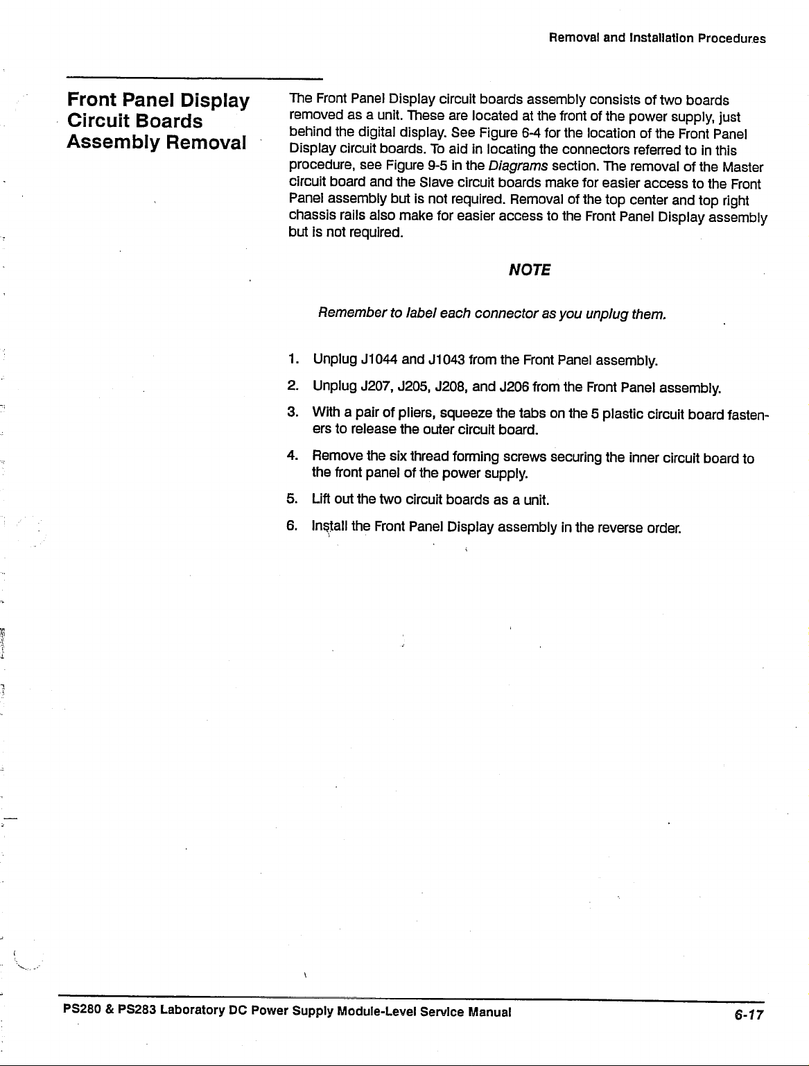
Front Panel Display
Circuit Boards
Assembly Removal
The Front Panel Display circuit boards assembly consists of two boards
removed as a unit. These are located at the front of the power supply, just
behind the digital display. See Figure 6-4 for the location of the Front Panel
Display circuit boards. To aid in locating the connectors referred to in this
procedure, see Figure 9-5 in the Diagrams section. The removal of the Master
circuit board and the Slave circuit boards make for easier access to the Front
Panel assembly but is not required. Removal of the top center and top right
chassis rails also make for easier access to the Front Panel Display assembly
but is not required.
wore
Remember to label each connector as you unplug them.
1.
Unplug J1044 and J1043 from the Front Panel assembly.
2.
Unplug J207, J205, J208, and J206 from the Front Panel assembly.
3. With a pair of pliers, squeeze the tabs on the 5 plastic circuit board fasteners to release the outer circuit board.
4.
Remove the six thread forming screws securing the inner circuit board to
the front panel of the power supply.
5. Lift out the two circuit boards as a unit.
6. Install the Front Panel Display assembly in the reverse order.
PS280 & PS283 Laboratory DC Power Supply Module-Level Service Manual
Page 60

Removal and Installation Procedures
REV AUG
Figure 6-4: Front Panel Display Assembly Removal
1991
Maintenance
Page 61

Removal and Installation Procedures
Front Panel Controls
Circuit Board
Removal
The Front Panel Controls circuit board Is located at the front of the power
supply. See Figure 6-5 for the location of the Front Panel Controls circuit
board.
To aid in locating the connectors referred to in this procedure, see
Figure 9-5 in the Diagrams section. The removal of other circuit boards is not
necessary to perform this procedure.
NOTE
Remember to label each connector as you disconnect them.
1.
Unplug connectors J3082, J5012, J1082, and J4043 from the Front Panel
Controls circuit board.
2.
Remove the CURRENT and VOLTAGE control knobs of both the MASTER
and SLAVE outputs by pulling them straight out.
3. Remove the nuts and washers from each of the four shafts.
4.
Slide the circuit board back, and lift out of the power supply.
5. Installation of the Front Panel Controls circuit board is done in the reverse
PS280 & PS283 Laboratory DC Power Supply Module-Level Service Manual
REV AUG
1991
Page 62

Removal and Installation Procedures
REV AUG
1991
Figure 6-5: Front Panel Controls Assembly
Maintenance
Page 63

Removal and Installation Procedures
Output Connectors
Circuit Board
Removal
The Output Connectors circuit board is located at the front of the power sup-
ply. See Figure 6-6 for the location of the Output Connectors circuit board. To
aid in locating the connectors referred to in this procedure, see Figure 9-1 in
the Diagrams section. The removal of other circuit boards is not necessary to
perform this procedure.
wore
Remember to label each connector as you disconnect them.
1.
Unplug connectors J106,
2.
Pull off the plastic cover over the power switch, located at the bottom left
of the front panel. This can be done by carefully prying the power switch
cover off with a small flat-blade screwdriver.
3. Remove the two screws securing the power switch.
4.
Remove the two screws that secure the entire front panel to the bottom
chassis of the power supply.
5. Slide the front panel forward, away from the bottom chassis.
6. Unplug the green ground wire from the chassis connector.
J4041,
J402, and J306 from the Master circuit
7. Remove the six tread forming screws securing the circuit board to the front
8. Installation of the Output Connectors circuit board is done in the reverse
PS280
& PS283 Laboratory DC Power Supply Module-Level Service Manual
REV AUG
1991
Page 64

Removal and Installation Procedures
Figure 6-6: Output Connectors Circuit Board and Power Switch Location
REV AUG
1991
Maintenance
Page 65

Removal and Installation Procedures
Power Transistor
Circuit Boards
Removal
The Power Transistor circuit boards are attached to the heat sink at the rear of
the instrument. See Figure 6-7 for the location of the Power Transistor circuit
boards. To aid in locating the connectors referred to in this procedure, see
Figure 9-6 in the Diagrams section. The removal of other circuit boards is not
necessary to perform this procedure.
1.
Unplug connector
circuit board you are removing.
2.
Remove the two screws securing each power transistor to the heat sink
and circuit board.
3. Unsolder the leads of the power transistors from the circuit board.
4.
Remove the power transistors from the power supply.
5. Remove the circuit board from the power supply.
6. Installation of the Power Transistor circuit board is done in the reverse
J1051
or
J3051,
depending on which Power Transistor
Slave Power
Transistor
Circuit Board
Figure 6-7: Power Transistor Circuit Boards Location
PS280
& PS283 Laboratory DC Power Supply Module-Level Service Manual
Master Power
Circuit Board
REV AUG
Transistor
1991
Page 66

•nW^WnnrLnn Options
^.-
Page 67

fMXlWUl. Options and Accessories
Power Cord Options
Some accessories are included with the PS280 or PS283. If you wish to purchase additional accessories, either optional or standard, see a Tektronix
products catalog, contact your local Tektronix field representative, or, in the
U. S., call the Tektronix National Marketing Center toll-free at 1-800-426-2200.
Option
AO
North American 120 V/6 A, 60 Hz, Tektronix part number
161-0248-00.
Option
A1
universal European 220 V/6 A, 50 Hz, Tektronix part number
161-0104-06.
Option A2 United Kingdom 240 V/6 A, 50 Hz, Tektronix part number
161-0104-07.
Option A3 Australian 120 V/6 A, 50 Hz, Tektronix part number 161-0104-05.
Option A4 North American 220 V/10 A, 60 Hz, Tektronix part number
161-0104-08.
Option A5 Switzerland 240 V/6 A, 50 Hz, Tektronix part number
161-0167-00.
Standard
Accessories
Optional Accessories "
The
PS280
(Tektronix part number 070-8355-00) is this manual.
Power cord Option A0 North American 120 V/6 A, 60 Hz (Tektronix part
number 1610248-00). See the section below for other power cords, which
can be ordered optionally.
three pairs of black and red test leads (Tektronix part number
196-3201-00).
The PS280 or
nix part number 070-8356-00) provides service information for maintenance
and repair of the PS280 or PS283 Laboratory DC Power Supply.
Any additional power cords for other countries.
or
PS283
PS283
Laboratory DC Power Supply Operator Manual
Laboratory DC Power Supply Service Manual (Tektro-
PS280 & PS283 Laboratory DC Power Supply Module-Level Service Manual
Page 68

B^SmXJAnnnn. Parts List
Page 69

mSSMJffinruinjTr
pans
ust
This section contains the list
or PS283 Laboratory DC Power Supply. These modules
tion
of
mechanical and electrical subparts.
identify and order replacement parts. Figures 8-1 and
ploded view
Parts Ordering Replacement parts are available from or
Information service center
Changes
improved components as they become available and
of the latest circuit improvements. Therefore, when ordering parts,
tant
to
• Part number
• Instrument type
• Instrument serial number
• Instrument modification number,
If a part you order has been replaced with a different
local Tektronix service center
change
of
all replaceable components.
or representative.
to
Tektronix instruments
include the following information
or
in
the part number.
of
replaceable modules that make up the PS280
are
model number
or
representative will contact you concerning
sometimes made
if
applicable
are
often a combina-
As
described below, use this list
8-2
provides
through
in
your local Tektronix,
to
your order:
or
to
accommodate
give you the benefit
improved part, your
an ex-
Inc.,
it is
impor-
to
any
PS280 & PS283 Laboratory
Module Replacement
The PS280
new, replacement modules
DC
Power Supply Module-Level Service Manual REVAUG
or
PS283
is
serviced
by
module replacement. You may purchase
in
the same way
as
other replacement parts.
1991
8-7
Page 70

Parts List
Using the Parts List
The
tabular information in the Parts List is arranged for quick
standing the structure and features of the list will help you find the all the
information you need for ordering replacement parts.
retrieval.
Item Names
Because
incomplete. For further Item Name identification, use the U.S. Federal Catalog-
ing Handbook
of
space limitations,
H6-1,
where available.
an
Item Name may sometimes appear
Indentation System
Indentation in this parts list shows the relationship between items. The following
is
an example
12
3 4 5
Assembly and/or Component
Attaching parts for Assembly and/or Component
Detail Part of Assembly and/or Component
Attaching parts
Parts
Attaching parts
of
the indentation system used in the Description column:
Name & Description
(END ATTACHING PARTS)
for
Detail Part
(END ATTACHING PARTS)
of
Detail Part
for
Parts
of
Detail Part
(END ATTACHING PARTS)
Under-
as
Attaching parts always appear
while the detail parts
included
separately, unless otherwise specified.
with,
the next higher indentation. Attaching parts must
are
at
indented
the same indentation as the item
to
the right. Indented items are part
Abbreviations
Abbreviations conform
dard
Y1.1.
to
American National Standards Institute (ANSI)
it
mounts,
be
purchased
of, and
stan-
8-2
REV AUG1991
Parts
Ust
Page 71

Parts List
Index Tektronix
No.
Part No.
8-1-1 200-3999-00
-2 367-0441-00
-3 211-0452-00
-4 211-0428-00
-5 213-0717-00
-6 118-8707-00
118-8749-00
148-0251-00
148-0251-00
148-0251-00
210-1025-00
210-0577-00
366-2172-00
211-0452-00
213-0119-00
118-8708-00
150-0154-00
150-0155-00
150-0154-00
150-0155-00
150-0154-00
Serial/Assembly No.
Effective Dscont
Qty. Name & Description
1 COVER.TOP
1 HANDLE W/END CAPS
5 SCREW,MACHINE,M3 X 0.5
2 SCREW.ASSEM WSHR.M3 X 0.5
6 SCREW,4-20.0.312,PNH THREAD FORMING
1 OUTPUT CIRCUIT BOARD
(PS280)
OUTPUT CIRCUIT BOARD
(PS283)
(ATTACHING PARTS)
.C405 CSE1 25V, 100UF
.C1151 CSE1 50V.100UF
.C1152 CSE1 50V.100UF
X 6
MM
X 6
L
MM
L
(PS280)
.C3151 CSE1 50V, 100UF
.C3152 CSE1 50V. 100UF
(PS280)
.D111 Diode 1N5402,
Diode 1N4004,
.0311 Diode 1N5402,
.0404 Diode 1N5402,
.JP59 JUMP WIRE
.JP60 JUMP WIRE
.J113 WIRE
V J1072 WIRE C. JD-0104-0014
.J4042 WIRE
.J5011 WIRE
.RL501 RELAY DC24V,
.RL502 RELAY DC24V,
.RL503 RELAY DC24V,
WASHER.FLAT.0.312 ID X 0.469
NUXPLAIN.HEX.0.281-32 X 0.375
CURRENT/VOLTAGE KNOB
SCREW.MACHINE.M3 X 0.5
SCREW.PNH.THREAD FORMING
FRONT PANEL CONTROL CIRCUIT BOARD
.C501 CSC 5OV 22UF
.C502 CSC 50V, 1000PF
.0503 CSC 50V,
.C504 CSM 50V.
.C505 CSC 50V,
0112 LED RED. LT6411G, 6*6M/M, LEDTECH
.D113 LED GREEN
.D312 LED RED,
.D313 LED GREEN
.D403 LED RED,
D501 Diode 1N4148, TOSH.HT
.0502 Diode 1N4148, TOSH.HT
.D503 Diode 1N4148, TOSH.HT
.D504 Diode 1N4148, TOSH.HT
.0505 Diode 1N4148, TOSH.HT
0506 Diode 1N4148. TOSH.HT
(PS280)
Diode 1N4004,
C.
0.
C.
(END ATTACHING PARTS)
(ATTACHING PARTS)
G.I.
G.I.
G.I.
G.I.
G.I.
0.6
0.6
JD-0104-0016
JD-0104-0015
JD-0105-5338
10A
10A
10A
X 6
0.01
UF
0.22UF
0.1
UF
LT6421,
6*6M/M, LEDTECH
LT6411
G.6*6M/M,
LT6421,
6*6M/M, LEDTECH
LT6411
G.6-6M/M.
OD X 0.031
MM
L
LEDTECH
LEDTECH
Mfr. Part No.
200-3999-00
367-0441-00
211-0452-00
211-0428-00
213-0717-00
118-8707-00
118-8749-00
2241-25107Z0
2241-5010720
2241-5010720
2241-5010720
2241-5010720
2501-N540200
2501-N400400
2501-N540200
2501-N400400
2501-N540200
4270-06D0000
4270-0600000
40WCJ1040016
40WCJ1040014
40WCJ1040015
40WCJ1055338
3312-2410140
3312-2410140
3312-2410140
210-1025-00
210-0577-00
366-2172-00
211-0452-00
213-0119-00
118-8708-00
2201-5022620
2201-5010220
2201-5010320
2221-50224J0
2201-5010420
3110-12D2060
3110-1502070
3110-1202060
3110-1502070
3110-1202060
2502-N4148T0
2502-N4148T0
2502-N4148T0
2502-N4148T0
2502-N4148T0
2502-N4148T0
PS280 & PS283 Laboratory DC Power Supply Module-Level Service Manual
REV AUG
1991
Page 72

Parts List
Index Tektronix
No.
Part No.
311-2404-00
311-2493-00
Serial/Assembly No.
Effective Dscont
Qty. Name
-Q501
v
& Description
Diode 1N4148.TOSH.HT
Diode 1N4148.TOSH.HT
Diode 1N4148.TOSH.HT
Zener VsW, 14.5V, HZ15-2, HITACHI
JUMP WIRE 0.6
JUMP WIRE 0.6
JUMP WIRE 0.6
JUMP WIRE 0.6
JUMP WIRE 0.6
JUMP WIRE 0.6
JUMP WIRE 0.6
JUMP WIRE 0.6
JUMP WIRE 0.6
JUMP WIRE 0.6
JUMP WIRE 0.6
JUMP WIRE 0.6
JUMP WIRE 0.6
JUMP WIRE 0.6
JUMP WIRE 0.6
JUMP WIRE 0.6
JUMP WIRE 0.6
JUMP WIRE 0.6
JUMP WIRE 0.6
WAFER B8B-XH-A
WAFER BOB-XH-A
WAFER B2B-XH-A
WAFER B5B-XH-A
TR 2SC 1815GR. TOSH
TR 2SA 1015GR, TOSH
TR2SC1815GR,'TOSH
RC%W. 47RJ. HT
RC6W. 47RJ, HT
RC%W, 22MJ, HT
RC'AW, 20KJ. HT
RC%W, 20KJ, HT
RC%W, 20KJ. HT
RCVHW,
20KJ,
HT
RC%W,82KJ.
HT
RCAW, 12KJ. HT
RCV.W. 4.7KJ. HT
RCy.W. 82KJ. HT
RC'AW. 33KJ. HT
RC'AW. 100RJ, HT
RC/.W, 30KJ. HT
RCy.W. 2.2MJ. HT
RC'/iW, 220KJ, HT
RC'AW, 10KJ, HT
RC'AW, 20KJ. HT
RM'AW. 30.1KF, HT
SW PUSH. SPUE22AE30
IC NE555R TEXAS
IC MC4N33. MOTO, (4N33, TFK)
(4N33.
GE)
VR10KB, 16A. RK163111R691
(RKDA10R691)
VR. 1KB. 16A, RK163111R717
(RK16110R19D)
Code Mfr. Part No.
2502-N4148T0
2502-N4148T0
2502-N4148T0
2503-1500051
4270-0600000
4270-O6D00O0
4270-0600000
4270-0600000
4270-06D0000
4270-0600000
4270-06DOOOO
4270-06D0000
4270-0600000
4270-0600000
4270-0600000
4270-0600000
4270-0600000
4270-06D0000
4270-06D0000
4270-0600000
4270-0600000
4270-0600000
4270-0600000
40WA-B8BXHA0
40WA-B9BXHA0
40WA-B2BXHA0
40WA-B5BXHA0
2602-1815GR0
2600-1015GR0
2602-1815GR0
2002-47B0JT0
2002-47B0JT0
2002-22B6JT0
2002-20B3JT0
2002-20B3JTO
2002-20B3JT0
2002-20B3JTO
2002-82B3JT0
2002-12B3JT0
2002-47B2JT0
2002-82B3JT0
2002-33B3JT0
2002-10B1JT0
2002-30B3JT0
2002-22B5JT0
2002-22B4JT0
2002-10B3JT0
2002-20B3JT0
2012-3012FT0
3202-1240610
2711-555P-00
2703-4N33-00
2110-103BC04
2110-102BC06
REV
AUG
1991
Parts Ust
Page 73

Parts List
Index Tektronix
No.
Part No.
311-2404-00
311-2493-00
260-2567-00
118-8711-00
118-8747-00
Serial/Assembly No.
Effective Dscont
Qty. Name & Description
.VR304 VR10KB, 16A, RK163111R691
.VR305 VR, 1 KB,
.VR501 SVR 10-M, 2KB, H, ± 100PM
1 S101 POWER SWITCH.4A.250 VAC
1 DISPLAY CIRCUIT BOARDS ASSEMBLY
1 DISPLAY CIRCUIT BOARDS ASSEMBLY
.C201 CSD 630V,
.C202 CSD 100V,
.C203 CSN 50V, 100PJ
.C204 CSD 100V.
.C205 CSK100V.0.47UJ
.C206 CSE1 16V.1000UZ
.C207 CSE1 16V.100U2
.C601 CSD 630V, 0.01 UJ
C602 CSD 100V, 0.1UJ
.C603 CSN 50V, 100PJ
.C6O4 CSD 100V.
.C605 CSK 100V,
.C606 CSE1 16V, 1000UZ
.C607 CSE1 16V, 100UZ
.0201 Diode 1N4004, G.I. HT
.0202 Diode 1N4004, G.I. HT
.0203 Diode 1N4004, G.I. HT
.D204 Diode 1N4004, G.I. HT
0205 DISPLAY RED GAP
.0206 DISPLAY RED GAP LTS546A1-NB, 0.5"
(RKDA10R691)
(RK16110R19D)
(PS280)
(PS283)
16A, RK163111R717
(END ATTACHING PARTS)
(ATTACHING PARTS)
0.01
UJ
0.1
UJ
0.22UJ
0.11UJ
0.47UJ
LTS546A1
-NB,
0.5"
Code Mfr. Part No.
2110-103BC04
2110-102BC06
2100-202BMOO
3202-1120710
118-8711-00
118-8747-00
2271-6A103J0
2271-1A104J0
2211-50101JO
2271-1A224J0
2291-1A474J0
2241-16108Z0
2241-16107Z0
2271-6A103J0
2271-1A104J0
2211-50101JO
2271-1A224J0
2291-1A474J0
2241-16108Z0
2241-16107Z0
2501-N4004T0
2501-N4004T0
2501-N4004T0
2501-N4O04T0
3131-12A5020
3131-12A5020
0207 DISPLAY RED GAP LTS546A1-NB, 0.5"
0208 DISPLAY RED GAP LTS546A1-NB, 0.5"
.0601 Diode 1N4004, G.I. HT
.0602 Diode 1N4004, G.I. HT
.0603 Diode 1N4004, G.I. HT
.0604 Diode 1N4004. G.I. HT
0605 DISPLAY RED GAP
.0608 DISPLAY RED GAP LTS546A1-NB. 0.5"
.0607 DISPLAY RED GAP LTS546A1-NB, 0.5"
.0608 DISPLAY RED GAP LTS546A1-NB, 0.5"
150-0161-00
150-0161-00
150-0161-00
150-0161-00
.0609 LED RED GAR LT9511G. 5, LEDTECH
0610 LED RED GAR LT9511G, 5. LEDTECH
D611 LED RED GAP, LT9511G, 5, LEDTECH
0612 LED RED GAR LT9511G.5. LEDTECH
JP1 JUMP WIRE 0.6
JP2 JUMP WIRE 0.6
.JP3 JUMP WIRE 0.6
.JP4 JUMP WIRE 0.6
(PS283 ONLY)
PS280 & PS283 Laboratory DC Power Supply Module-Level Service Manual
LTS546A1
-NB.
0.5"
REV AUG
3131-12A5020
3131-12A5020
2501-N4004T0
2501-N4004T0
2501-N4O04T0
2501-N4004TO
3131-12A5020
3131-12A5020
3131-12A5020
3131-12A5020
3111-0200130
3111-0200130
3111-0200130
3111-0200130
4270-06DO0O0
4270-06DOOOO
4270-0600000
4270-0600000
1991
Page 74

Parts List
Index Tektronix
No.
Part No.
Serial/Assembly No.
Effective Dscont
Qty. Name & Description
JUMP WIRE 0.6
JUMP WIRE 0.6
JUMP WIRE 0.6
JUMP WIRE 0.6
(PS283 ONLY)
JUMP WIRE 0.6
JUMP WIRE 0.6
JUMP WIRE 0.6
JUMP WIRE 0.6
JUMP WIRE 0.6
JUMP WIRE 0.6
JUMP WIRE 0.6
JUMP WIRE 0.6
JUMP WIRE 0.6
JUMP WIRE 0.6
JUMP WIRE 0.6
JUMP WIRE 0.6
JUMP WIRE 0.6
JUMP WIRE 0.6
JUMP WIRE 0.6
JUMP WIRE 0.6
JUMP WIRE 0.6
JUMP WIRE 0.6
JUMP WIRE 0.6
JUMP WIRE 0.6
JUMP WIRE 0.6
JUMP WIRE 0.6
JUMP WIRE 0.6
JUMP WIRE 0.6
JUMP WIRE 0.6 '
JUMP WIRE 0.6
JUMP WIRE 0.6
JUMP WIRE 0.6
JUMP WIRE 0.6
JUMP WIRE 0.6
JUMP WIRE 0.6
(PS283 ONLY)
JUMP WIRE 0.6
WAFER B2B-XH-A
WAFER B2B-XH-A
WAFER B2B-XH-A
WAFER B2B-XH-A
RMV«W, 1KF, HT
RM'/iW, 1MF
RM'/«W. 267RF. HT
RM%W. 4.99KF, HT
RM%W. 267RF. HT
RC'AW, 47KJ, HT
RM'AW, 100KF, HT
RC/.W. 470RJ, HT
RC%W. 470RJ. HT
RM'AW. 27 KF, HT
(TEST SELECTED)
RM%W. 27
RM%W.
1KF,
RM'/aW, 1MF
RM%W. 267RF, HT
RM%W. 4.99KF, HT
KF.
HT
HT
Mfr. Part No.
4270-06DOOOO
4270-O6D0OO0
4270-06DOO0O
4270-0600000
4270-06DOOOO
4270-O6D0O0O
4270-O6DO0OO
4270-0600000
4270-06DOOOO
4270-06DOOOO
4270-0600000
4270-O6D00O0
4270-06D0000
4270-O6DOO0O
4270-O6D0O0O
4270-0600000
4270-O6D0OO0
4270-O6DO000
4270-0600000
4270-06DOOOO
4270-O6D0OO0
4270-0600000
4270-06DOOOO
4270-0600000
4270-O6D0000
4270-0600000
4270-0600000
4270-06DOOOO
4270-06DOOOO
4270-06DOOOO
4270-0600000
4270-0600000
4270-06DOOOO
4270-06D0000
4270-06DOOOO
4270-06DOOOO
40WA-B2BXHA0
40WA-B2BXHA0
40WA-B2BXHAO
40WA-B2BXHA0
2012-1001FTO
2013-1004FOO
2012-2670FT0
2012-4991FTO
2012-2670FT0
2002-47B3JTO
2012-1003FT0
2002-47B1JTO
2002-47B1JTO
2012-2702FT0
2012-2702FT0
2012-1001FTO
2013-1004F00
2012-2670FT0
2012-4991FTO
REV AUG
1991
Parts List
Page 75

Parts List
Index Tektronix
No.
Part No.
260-2568-00
260-2568-00
156-1435-00
-15 213-0717-00
-16 211-0785-00
-17 211-0785-00
Serial/Assembly No.
Effective Dscont Qty. Name & Description
.R608 RM%W, 267RF, HT
.R609 RC'AW, 47KJ, HT
.R610 RM'/4W, 100KF. HT
.R611 RCV.W, 47ORJ, HT
.R612 RCV.W. 47ORJ, HT
.R613 RM'AW, 27 KF, HT
(TEST SELECTED)
.R614 RM'AW, 27 KF, HT
.R2011 RM'/aW.SOOKF
.R2012 RM%W, 500KF
.R6011 RM'/aW, 500KF
.R6012 RM'AW, 500KF
.S201 SW SILDE SSS342NB4-GW, O.1A
S202 SW SILDE SSS342NB4-GW, O.1A
.U201 IC ICL7107CPL (ICL7107SCPL).
INTERSIL (TSC7107CPL)
U202 IC UA431AWC, FAIR, NS
.U203 IC UA7805UC, FAIRCHILD (LM7805CT,
.U601 IC ICL7107CPL (ICL7107SCPL),
.U602 IC UA431AWC, FAIR, NS
.U6O3 IC UA7805UC, FAIRCHILD (LM7805CT,
.VR201 SVR 1O-M,
.VR202 SVR 1O-C, 1OKB, H
VR601 SVR 10-M,
.VR602 SVR 10-C, 10KB, H
.XU201 IS40RD, N
.XU203 HS HS-GSP-13A, MB-210
.XU601 IS40P, D, N
.XU603 HS HS-GSP-13A, MB-210
SCREW.4-20 X
SCREW.MACHINE.M3 X 6 MM
SCREW.MACHINE.M3 X 6 MM
NS) (AN7805 MATS)
INTERSIL (TSC7107CPL)
NS) (AN7805 MATS)
(PS280)
SVR 10-C, 470RB. H
SVR 10-C. 470RB. H
(END ATTACHING PARTS)
0.312.PNH.THREAD
2KB.
2KB,
± 1O0PPM
± 100PPM
FORMING
Mfr. Part No.
2012-2670FT0
2002-47B3JTO
2012-1003FT0
2002-47B1JTO
2002-47B1JT0
2012-2702FT0
2012-2702FT0
2013-5003F00
2013-5003F00
2013-5O03F0O
2013-5003F00
3204-0240170
3204-0240170
2712-7107CPL
2711 -431CPLZ
2701-7805UCZ
2712-7107CPL
2711-431
2701-7805UCZ
2100-202BM01
2100-103BC01
2100-471BC01
2100-202BM01
2100-103BC01
2100-471BC01
3612-40D000N
5207-AF000210
3612-40DOOON
2701-7805UCZ
213-0717-00
211-0785-00
211-0785-00
CPLZ
PS280 & PS283 Laboratory DC Power Supply Module-Level Service Manual
REV AUG
1991
Page 76

Parts List
REV AUG
1991
Figure
8-1:
Exploded View A
Parts List
Page 77

Parts List
Index Tektronix
No.
Part
8-2-1
-2 118-8709-00
-10 211-0498-00
-11 211-0728-00
No.
118-8706-00
118-8748-00
159-0339-00
159-0191-00
159-0338-00
159-0338-00
159-0339-00
159-0191-00
159-0338-00
159-0338-00
159-0339-00
159-0312-00
159-0312-00
129-1414-00
129-1412-00
211-0784-00
213-0717-00
118-8712-00
220-0085-00
118-8710-00
Serial/Assembly
Effective Dscont
No.
Qty.
Name & Description
FUSE CIRCUIT BOARD
(PS280)
FUSE CIRCUIT BOARD
(PS283)
(ATTACHING PARTS)
.F102 FUSE.5
.F102 FUSE.5
.F103 FUSE.5
.F104 FUSE.5
.F105 FUSE.5
.F105 FUSE.5X20MM.2A.250V
.F106 FUSE.5
.F107 FUSE.5
.F108 FUSE.5
.F109 FUSE.5
.F110 FUSE.5
J113 WIRE
.J313 WIRE
J1041 WAFER B2B-XH-A
.J1042 WAFER B2B-XH-A
AC SELECTOR CIRCUIT BOARD
.S102 SW SLIDE SDKGA4, F7422070M
.8103 SW SLIDE SDKGA4, F7422070M
SPACER.POST.32.5 MM
SPACER.POST.30 MM
SCREW.MACHINE.M3
SCREW.SELF TAPPING.4-20
TRANSISTOR CIRCUIT BOARD.SLAVE
.J1051 WAFER B4P-VH
.Q3071
TR 2N
.Q3072
TR
NUT.PLAIN.HEX.M3 X5.5
TRANSISTOR CIRCUIT BOARD.MASTER
J3051 WAFER B8P-VH
.Q402
TR
.Q1071
TR 2N
.01072
TR
SCREW.MACHINE.M3
SCREW.MACHINE.M3
X 20
MM.5A.250V
(PS280)
X 20
MM.2A.250V
(PS283)
X 20
MM.0.315A.250V
X 20
MM.0.315A.250V
X 20
MM.5A.250V
(PS280)
X 20
MM.0.315A.250V
X 20
MM.0.315A.250V
X 20
MM.5A.250V
X 20
MM.0.25A.250V
X 20
MM.0.25A.250V
C.
JD-0104-0016
C.
JD-0104-0016
(END ATTACHING PARTS)
(ATTACHING PARTS)
(SDKGA4274A)
(SDKGA4274A)
(END ATTACHING PARTS)
L
L
X 8 MM
(ATTACHING PARTS)
3055, TOSH
2N 3055. TOSH
(END ATTACHING PARTS)
(ATTACHING PARTS)
2N 3055, TOSH
3055. TOSH
2N 3055, TOSH
(END ATTACHING PARTS)
(2N
(2N
MM
(2N
(2N
(2N
X 12 MM
X 0.5 X 16 MM
X 0.312
3055,
3055,
3055.
3055,
3055,
ST)
ST)
ST)
ST)
ST)
Mfr.
Part
No.
118-8706-00
118-8748-00
37FT-1124502
37FT-1124502
37FT-1124311
37FT-1124311
37FT-1124502
37FT-1124502
37FT-1124311
37FT-1124311
37FT-1124311
37FT-1124251
37FT-1124251
40WCJ1040016
40WCJ1040016
40WA-B2BXHA0
40WA-B2BXHA0
118-8709-00
3204-0220180
3204-0220180
129-1414-00
129-1412-00
211-0784-00
213-0717-00
118-8712-00
40WA-B4PVH00
2610-3055-00
2610-3055-00
220-0085-00
118-8710-00
40WA-B8PVH00
2610-3055-00
2610-3055-00
2610-3055-00
211-0498-00
211-0728-00
PS280 & PS283 Laboratory DC Power Supply Module-Level Service Manual
REV AUG
1991
8-9
Page 78

Parts List
Index Tektronix
No.
Part No.
-12 118-8705-00
118-8746-00
Serial/Assembly No.
Effective Dscont
Qty. Name & Description
MASTER CIRCUIT BOARD
(PS280)
MASTER CIRCUIT BOARD
(PS283)
(ATTACHING PARTS)
.C102 CSE1 4700UF.63V
.C109 CSE1 25V, 47UZ, 8@
.C110 CSD 630V.
.C111 CSD 100V. 0.1UJ, 13*9*4
.C112 CSC50V, 500PJ
.0113 CSN 50V, 33PJ. 6@
.C302 CSE1 4700UR63V
.C309 CSE1 25V, 47UZ, 8@
.C310 CSD 630V,
.C311 CSD 100V.0.1UJ. 13*9*4
.0312 CSC 50V, 500PJ
.0313 CSN 50V.33PJ, 6@
.0403 CSC 50V, 1000PK
.C404 CSC50V, 1000PK
.01141 CSE1 50V,
.01142 CSE1 50V. 4.7UZ
.C3141 CSE1 50V, 4.7UZ
. .03142 CSE1 50V. 4.7UZ
.DL1 Wire C.
.DL2 Wire C. JD-2101-2564
0103 Zener %W.
.D104 Zener %W.11.9V-12.4V, HZ12A2.
.D105 Diode 1N4148, TOSHfTFK, PHIL, FAIR),HT
010B Zener V2W,
0107 Diode 1N4148, TOSHfTFK, PHIL, FAIRJ.HT
.D108 Diode 1N4148, TOSHfTFK, PHIL, FAIRJ.HT
.0109 Zener %W,
.0110 Diode 1N5402. G.I.
.D116 Diode 1N4148, TOSHCTFK, PHIL, FAIRJ.HT
.D303 Zener %W.
.D304 Zener '/2W,11.9V-12.4V, HZ12A2,
.D305 Diode 1N4148, TOSHfTFK. PHIL. FAIR),HT
.0306 Zener VaW,
0307 Diode 1N4148. TOSHfTFK, PHIL. FAIR).HT
.D308 Diode 1N4148. TOSHCTFK, PHIL. FAIR),HT
.D309 Zener'/aW,
.0310 Diode 1N5402, G.I.
.0316 Diode 1N4148, TOSH
.0402 Diode 1N4148. TOSH
.JP1 JUMP WIRE 0.6
(PS280)
CSE1 2200UF.63V
0.01 UJ,
(PS280)
CSE1 2200UF.63V
0.01 UJ.
4.7U2
JD-2101
5.0V-5.2V,
Hitachi Only
Hitachi Only
8.89V-9.29V,
NEC Only
8.89V-9.29V,
NEC Only
5.0V-5.2V.
Hitachi Only
Hitachi Only
8.89V-9.29V.
NEC Only
8.89V-9.29V.
NEC Only
13*4*9
13*4*9
-2564
HZ5C2.
RD9.1
RD9.1
HZ5C2.
RD9.1
RD9.1EB3.
EB3.
EB3.
EB3,
Mfr. Part No.
118-8705-00
118-8746-00
2241-63478Z0
2241-63228Z0
2241-25476Z0
2271-6A103J0
2271-1A104J0
2201-50501JO
2211-50330J0
2241-63478Z0
2241-63228Z0
2241-25476Z0
2271-6A103J0
2271-1A104J0
2201-50501 JO
2211-50330J0
2201-50102K0
2201-50102K0
2241-50475ZO
2241-50475Z0
2241-50475Z0
2241-5O475Z0
40WCJ7012564
40WCJ7012564
2503-0510050
2503-1200050
2502-N4148T0
2503-0910050
2502-N148T0
2502-N148T0
2503-0910050
2501-N540200
2502-N4148T0
2503-0510050
2503-1200050
2502-N4148T0
2503-0910050
2502-N4148T0
2502-N4148T0
2503-0910050
2501-N540200
2502-N4148T0
2502-N4148T0
4270-06D0000
REV AUG
1991
Parts Ust
Page 79

Parts List
Index Tektronix
No.
Part No.
Serial/Assembly No.
Effective Dscont
Qty. Name & Description
JUMP WIRE
JUMP WIRE
JUMP WIRE
JUMP WIRE
JUMP WIRE
JUMP WIRE
JUMP WIRE
JUMP WIRE
JUMP WIRE
JUMP WIRE
JUMP WIRE
JUMP WIRE
JUMP WIRE
JUMP WIRE
JUMP WIRE
JUMP WIRE
JUMP WIRE
JUMP WIRE
JUMP WIRE
JUMP WIRE
JUMP WIRE
JUMP WIRE
JUMP WIRE
WAFER B2P-VH
WAFER JD-PI-5002
WAFER B2P-VH
WAFER JD-PI-5002
WAFER B2P-VH
WAFER B3P-VH
WAFER B8P-VH
WAFER B4P-VH
WAFER B4B-XH-A
WIRE
C.JD-0110-0017
WAFER B6P-VH
WAFER B4P-VH
WIRE
C.
JD-0111-0001
WAFER B4B-XH-A
TR 2SC 1815GR, TOSH
TR 2SD 880Y, TOSH
TR 2SC 1815GR, TOSH
TR 2SA 1015GR, TOSH
TR 2SC 1815GR. TOSH
TR 2SD 880Y TOSH
TR 2SC 1815GR, TOSH
TR 2SA 1015GR, TOSH
TR 2SD 880Y TOSH
RM%W.
2KF.
RM'AW. 10K,
RC'/iW, 150KJ.
RC%W. 68RJ,
RCV,W,
1.5KJ,
RCV«W, 1KJ.
RC'/,W,
1.5KJ,
RC'AW, 13KF,
RM'/iW,
30.1 KF,
RCVHW,
4.7MJ, HT
RC'/iW. 10MJ.HT
0.6
0.6
0.6
0.6
0.6
0.6
0.6
0.6
0.6
0.6
0.6
0.6
0.6
0.6
0.6
0.6
0.6
0.6
0.6
0.6
0.6
0.6
0.6
HT
HT
HT
HT
HT
HT
HT
HT
HT
Mfr. Part No.
4270-O6D00O0
4270-06D0000
4270-06D0000
4270-0600000
4270-0600000
4270-06D0000
4270-0600000
4270-06D0000
4270-06DOOOO
4270-06D0000
4270-06DOOOO
4270-0600000
4270-0600000
4270-06D0000
4270-0600000
4270-0600000
4270-0600000
4270-0600000
4270-0600000
4270-O6D00O0
4270-06DOOOO
4270-0600000
4270-0600000
40WA-B2PVH00
40WAJ500P020
40WA-B2PVH00
40WAJ500P020
40WA-B2PVH0O
40WA-B3PVH00
40WA-B8PVH00
40WA-B4PVH00
40WA-B4BXHA0
40WCJ1100017
40WA-B6PVH00
40WA-B4PVH00
40WCJ1110001
40WA-B4BXHA0
2602-1815GR0
2603-880Y-00
2602-1815GR0
2600-1015GR0
2602-1815GR0
2603-880Y-00
2602-1815GR0
2600-1015GR0
2603-880Y-00
2012-2001FTO
2012-1002FTO
2002-15B4JT0
2002-68BOJTO
2002-15B2JT0
2002-10B2JT0
2002-15B2JT0
2012-1302FTO
2012-3012FT0
2002-47B5JT0
2002-10B6JT0
PS280 & PS283 Laboratory DC Power Supply Module-Level Service Manual
REV AUG
1991
Page 80

Parts List
Index Tektronix
No.
Part
No.
Serial/Assembly
Effective Dscont
No.
Qty.
Name & Description
RC'AW,
RC'AW,
RC'AW,
RC'AW,
RC'AW,
JUMP WIRE
RC'AW,
RO
RC'AW.
RC'AW,
RR2W.150RJ
RM%W.
RMV«W,
RC'AW,
RC'AW,
RC'AW.
RC'AW,
RC'AW,
RM'AW,
RM'AW,
RC'AW,
RC'AW,
RC'AW,
RC'AW.
RC'AW.
RC'AW.
RC'AW.
JUMP WIRE
RC'AW.
R0
RC'AW.
RC'AW,
RC'AW,
RR 2W,
RC'AW,
RC'AW.
RC'AW.
RC'AW.
RC'AW.
RR5W,
RC'AW.
RC'AW,
RC'AW,
RC'AW,
RC'AW,
RC'AW.
RR5W,
(PS280)
RR5W.
(PS283)
RC'AW,
RC'AW.
RC'AW,
RC'AW,
RC'AW,
RC'AW.
RC'AW,
2W,
2W.
2.7KJ. HT
1KJ, HT
180RJ, HT
1OKJ. HT
51
ORJ.
0.6@, HT
51ORJ, HT
1KJ
3.3KJ, HT
150KJ, HT
2KF,
HT
10KF. HT
150KJ. HT
68RJ, HT
1.5KJ,
HT
1KJ. HT
1.5KJ,
HT
13KF, HT
3O.1KF, HT
4.7MJ, HT
10MJ. HT
2.7KJ, HT
1KJ, HT
180RJ. HT
19KJ. HT
51
ORJ,
0.6@, HT
51
ORJ,
1KJ
3.3KJ. HT
150KJ, HT
4.7MJ, HT
150RJ
3.6KJ. HT
3KJ. HT
1.2KJ.
HT
2.7KJ, HT
1KJ, HT
0.3RJ.
+100PPM
19KJ. HT
19KJ. HT
1.2KJ,
HT
1.5KJ.HT
2.4KJ, HT
2.4KJ, HT
0.3RJ,
±100PPM
0.5RJ,
+100PPM
1KJ. HT
1KJ, HT
47RJ. HT
47RJ, HT
4.7KJ, HT
4.7KJ, HT
4.7KJ, HT
HT
HT
HT
Mfr.
Part
No.
2002-27B2JT0
2002-10B2JT0
2002-18B1JY0
2002-10B3JT0
2002-51B1JT0
4270-06D0000
2002-51B1JT0
2075-10B2J00
2002-33B2JT0
2002-15B4JT0
2035-1500JOO
2012-2001FTO
2012-1002FT0
2002-15B4JT0
2002-68B0JT0
2002-15B2JT0
2002-10B2JT0
2002-15B2JT0
2012-1302FT0
2012-3012FT0
2002-47B5JTO
2002-10B6JT0
2002-27B2JTO
2002-10B2JT0
2002-18B1JT0
2002-10B3JT0
2002-51B1JT0
4270-O6D0000
2002-51B1JT0
2075-10B2JO0
2002-33B2JT0
2002-15B4JT0
2002-47B5JT0
2035-1500J00
2002-36B2JT0
2002-30B2JT0
2002-12B2JT0
2002-27B2JT0
2002-10B2JT0
2037-3BBDJ00
2002-10B3JT0
2002-10B3JT0
2002-12B2JT0
2002-15B2JT0
2002-24B2JT0
2002-24B2JT0
2037-3BBDJ00
2037-5BBDJ00
2002-10B2JT0
2002-10B2JT0
2002-47B0JT0
2002-47BOJTO
2O02-47B2JT0
2002-47B2JT0
2002-47B2JT0
REV AUG
1991
Parts
Ust
Page 81

Parts Ust
Index Tektronix
No.
Part No.
Serial/Assembly No.
Effective Dscont
Qty. Name & Description
RC'AW, 4.7KJ, HT
RC/.W, 2.4KJ, HT
RC'AW, 2.4KJ, HT
RC'/.W, 1KJ. HT
RC%W,
1KJ.
RC'AW, 47RJ, HT
RCV«W, 47RJ, HT
RC%W, 4.7KJ, HT
RC'/«W, 4.7KJ, HT
RC'/dW, 4.7KJ, HT
RC%W, 4.7KJ, HT
RR5W, 0.3RJ, +100PPM
(PS280)
RR5W. 0.5RJ, +100PPM
IC UA431AWC, FAIR, NS
IC UA741CR TEXAS (UA741TC. FAIR)
IC LM301AR TEXAS
IC UA741CR TEXAS (UA741TC, FAIR)
IC UA431AWC. FAIR, NS
IC UA741CR TEXAS (UA741TC, FAIR)
IC LM301AR TEXAS
IC UA741CR TEXAS (UA741TC, FAIR)
IC UA723CN, TEXAS (SIGNETICS)
IC UA741CR TEXAS (UA741TC, FAIR)
HT
Code Mfr. Part No.
2002-47B2JT0
2002-24B2JT0
2002-24B2JT0
2002-10B2JT0
2002-10B2JT0
2002-47B0JT0
. 2002-47B0JT0
2002-47B2JT0
2002-47B2JT0
2002-47B2JT0
2O02-47B2JT0
2037-3BBDJO0
2037-5BBDJOO
2711-431CLPZ
2711-741CP-0
2711-301AP-0
2711-741CP-0
2711-431CLPZ
2711-741CP-0
2711-301AP-0
2711-301AP-0
2711-723CN-0
2711-301 AP-0
-13 211-0428-00
-14 213-1037-00
-15 210-0011-00
-16 200-3998-00
-17 120-5007-00
120-5006-00
-18 211-0751-00
-19 118-8704-00
118-8750-00
SVR 10-M, 2KB. H. ± 100PM
SVR 10-C, 2.2KB, H
SVR 10-C, 3.3KB, H
SVR 10-M, 2KB. H, ± 100PM
SVR 10-C, 2.2KB, H
SVR 10-C, 3.3KB, H
SVR 10-C, 22KB, H
SVR 10-C, 1KB. H
SVR 10-C. 1KB, H
SVR 10-C, 1KB. H
SVR 10-C. 10KB. H
(END ATTACHING PARTS)
2 SCREW.ASSEM WSHR.M3 X 0.5 X 6 MM L
4 SCREW.MACHINE.M5X12
4 WASHER.LOCK.0.25 ID.0.025 THK
1 COVER.BOTTOM
RANSFCRMER
TS101 TRANSFORMER
(PS283)
2 SCREW.ASSEMWSHR.M3X8
SLAVE CIRCUIT BOARD
(PS280)
SLAVE CIRCUIT BOARD
(PS283)
(ATTACHING PARTS)
CSE1 35V, 470UZ
CSE1 35V, 470UZ
CSE1 25V, 100UZ
CSE1 25V, 1O0UZ
CSM
50V,
0.01 UJ
2100-202BM00
2100-222BC01
2100-332BCOO
2100-202BM00
2100-222BC01
2100-332BCO0
2100-223BCO0
2100-102BCOO
2100-102BCOO
2100-102BCOO
2100-103BC01
211-0428-00
213-1037-00
211-0011-00
200-3998-00
120-5007-00
120-5006-00
211-0751-00
118-8704-00
118-8750-00
2241-35477Z0
2241-35477Z0
2241-25107Z0
2241-25107Z0
2221-50103J0
PS280 & PS283 Laboratory DC Power Supply Module-Level Service Manual
REV AUG
1991
Page 82

Parts List
Index Tektronix
No.
Part
No.
Serial/Assembly
Effective Dscont
No.
Qty. Name & Description
CSM 50V.0.01UJ
(PS280 ONLY)
CSE1 35V, 470UZ
CSE1 35V. 470UZ
CSE1 25V, 100UZ
CSE1 25V, 100UZ
CSM 50V.0.01UJ
CSM 50V.0.01UJ
(PS280 ONLY)
CSE1 25V, 6800UZ
Diode 1N4148, TOSH.
Diode 1N4148, TOSH,
Diode 1N4148, TOSH,
Diode 1N5402,
Diode 1N5402,
Diode 1N5402,
Diode 1N5402,
Diode 1N4004, G.I.
Diode 1N4004, G.I.
Diode 1N4004. G.I.
Diode 1N4004. G.I.
DIODE 1N5402,
DIODE 1N5402.
DIODE 1N5402,
DIODE 1N5402,
DIODE 1N5402,
DIODE 1N5402,
DIODE 1N5402,
DIODE 1N5402
JUMP WIRE
JUMP WIRE
JUMP WIRE
JUMP WIRE
JUMP WIRE
JUMP WIRE
JUMP WIRE
JUMP WIRE
JUMP WIRE
JUMP WIRE
JUMP WIRE
JUMP WIRE
JUMP WIRE
JUMP WIRE
JUMP WIRE
JUMP WIRE
JUMP WIRE
WAFER JD-PI-5004
WAFER JD-PI-5004
WAFER B2P-VH
WAFER B6P-VH
WAFER B12B-XH-A
TR2SA 1015GR, TOSH
TR2SA715C, HITACHI
TR 2SC 1815GR, TOSH
(PS280 ONLY)
TR2SC1815GR.TOSH
(PS280 ONLY)
G.I.
G.I.
G.I.
G.I.
G.I.
G.I.
G.I.
G.I.
G. I.
G. I.
G. I.
;
HT
HT
HT
HT
HT
HT
HT
Mfr. Part
2221-50103J0
2241-35477Z0
2241-35477Z0
2241-25107Z0
2241-25107Z0
2221-50103J0
2221-50103J0
2241-25688Z0
2502-N4148T0
2502-N4148T0
2502-N4148T0
2501-N540200
No.
2501-N540200
2501-N540200
2501-N540200
2501-N4004TO
2501-N4004T0
2501-N4004T0
2501-N4004TO
2501-N540200
2501-N540200
2501-N540200
2501-N540200
2501-N54D200
2501-N54D200
2501-N54D200
2501-N54D200
427O-O6D00O0
4270-06D0000
4270-06DOOOO
4270-06DOOOO
427O-O6DO0O0
4270-O6DO0O0
4270-06D0000
427O-06DOOO0
427O-06DO000
427O-O6D0O00
4270-0800000
4270-O6DO000
4270-06DOOOO
4270-06D0000
4270-06DOOOO
4270-06D0000
4270-06D0000
40WAJ500P040
40WAJ500P040
40WA-B2PVH00
40WA-B6PVH0O
40WAB1BXHAO
2600-1015GR0
2600-715C-00
2602-1815GR0
2602-1815GR0
REV AUG
1991
Parts List
Page 83

Parts List
Index Tektronix
No.
Part No.
148-0251-00
148-0251-00
148-0251-00
148-0251-00
-20 211-0751-00
159-0233-00
159-0226-00
Serial/Assembly No.
Effective Dscont Qty. Name & Description
.0110 TR2SA1015GR.TOSH
.0111 TR2SC1815GR.TOSH
.Q112 TR 2SC 1815GR, TOSH
.0301 TR 2SA 1015GR, TOSH
.0302 TR 2SA715C, TOSH
.0308 TR 2SC 1815GR, TOSH
.0309 TR 2SC 1815GR, TOSH
.0310 TR 2SA 1015GR, TOSH
.0311 TR 2SC 1815GR, TOSH
.0312 TR 2SC 1B15GR. TOSH
.RL101 RELAY DC24V, 10A
.RL102 RELAY DC24V, 10A
.RL301 RELAY DC24V. 10A
.RL302 RELAY DC24V. 10A
.R102 RC'AW, 10KJ, HT
.R103 RM'AW. 11.3KF, HT
.R104 RM'AW, 10.5KF, HT
.R133 RC'AW. 4.7KJ, HT
.R134 RC'AW, 15KJ. HT
.R135 RC'AW, 10KJ, HT
.R136 RC'AW, 4.7KJ, HT
.R137 RC'AW, 27KJ. HT
.R138 RC'AW, 15RJ, HT
.R139 RC'AW.ISKJ.HT
.R140 RC'AW. 15RJ, HT
.R141 RC'AW. 30KJ, HT
.R142 RC'AW.
.R301
.R302 RC'AW, 10KJ, HT
.R303 RM'AW, 11.3KF, HT
.R304 RM'AW, 10.5KF, HT
.R333 RC'AW. 4.7KJ, HT
.R334 RC'AW, 15KJ, HT
.R335 RC'AW, 19KJ, HT
.R336 RC'AW. 4.7KJ, HT
.R337 RC'AW, 27KJ, HT
.R338 RC'AW, 15RJ, HT
R339 RC'AW, 15KJ, HT
.R340 RC'AW, 15RJ, HT
.R341 RC'AW. 30KJ, HT
.R342 RC'AW,
.R401 RC 1W, 470RJ
U101 IC UA7815UC, FAIR (AN7815, MATS)
U301 IC UA7815UC, FAIR (AN7815, MATS)
3 SCREW.ASSEM WSHR.M3 X 8
1 F101 FUSE, 4A.250V.FAST
1 F101 FUSE. 2.5A.250V.FAST
(PS280 ONLY)
(PS280 ONLY)
(PS280 ONLY)
(PS280 ONLY)
(PS280 ONLY)
(PS280 ONLY)
9.1 KJ,
RO
3W,
4.7KJ
9.1 KJ,
(L7815CV ST)
(L7815CVST)
(END ATTACHING PARTS)
POWER SOCKET RECEPTACLE
(PS280)
(PS283)
HT
HT
Mfr. Part No.
2600-1015GRO
2602-1815GR0
2602-1815GR0
260O-1015GR0
2600-715C-00
2602-1815GR0
2602-1815GR0
2600-1015GR0
2602-1815GR0
2602-1815GR0
3312-2410140
3312-2410140
3312-2410140
3312-2410140
2002-10B3JT0
2012-1132FT0
2012-1052FT0
2002-47B2JT0
2002-15B3JT0
2002-10B3JT0
2002-47B2JT0
2002-27B3JT0
2002-15B0JT0
2002-15B3JT0
2002-15BOJT0
2002-30B3JT0
2002-91B2JT0
2076-47B2J00
2002-10B3JT0
2012-1132FT0
2012-1052FT0
2002-47B2JT0
2002-15B3JT0
2002-10B3JT0
2002-47B2JT0
2002-27B3JT0
2002-15B0JT0
2002-15B3JT0
2002-15B0JT0
2002-30B3JT0
2002-91B2JT0
2004-47B1J00
2701-7815UCZ
2701-7815UCZ
211-0751-00
3610-0060030
159-0233-00
159-0226-00
PS280 & PS283 Laboratory DC Power Supply Module-Level Service Manual
REV AUG
1991
Page 84

Parts List
REV AUG
1991
Figure 8-2: Exploded View B
Parts List
Page 85

Parts List
Index Tektronix
No.
Part No.
070-8355-00
161-0248-00
196-3201-00
070-8356-00
161-0104-06
161-0104-07
161-0104-05
161-0104-08
161-0167-00
Serial/Assembly No.
Effective Dscont
Qty. Name & Description
Standard Accessories
1 PS280 & PS283 Operators Manual
1 Power Cord, Option AO.North American,
120 V/6 A.60HZ
1 Test Lead, Set of 3 Pairs
Optional Accessories
PS280 & PS283 Service Manual
Power Cord, Option
220 V/6 A.SOHz
Power Cord, Option A2,United Kingdom,
240 V/6 A,50Hz
Power Cord, Option A3,Australian, 120 V/6 A,50Hz
Power Cord, Option A4,North American,
220 V10 A.60HZ
Power Cord, Option A5,Switzerland, 240 V6 A.SOHz
A1
.Universal European,
Mfr. Part No.
070-8355-00
161-0248-00
196-3201-00
070-8356-00
161-0104-06
161-0104-07
161-0104-05
161-0104-08
161-0167-00
PS280 & PS283 Laboratory DC Power Supply Module-Level Service Manual
Page 86

BBiimmnnnri Diagrams
w
Page 87

fSJDiagrams
and Circuit Board Illustrations
This section contains the circuit board illustrations and schematic diagrams
this power supply.
Component Values Electrical components shown on the diagrams are in the following units unless
noted otherwise:
Capacitors: Values one
one are in microfarads
Resistors: Values are
or
greater are in picofarads (pF). Values less than
(JJ.F).
in
Ohms (Q).
for
PS280
& PS283 Laboratory DC Power Supply
Module-Level
Service Manual
9-7
Page 88

JP03
o
1
I
C112
Hf
QP
s
0304
J4041
t
I
I
I VR403
s
)
PS280 & PS283 Laboratory
DC
Power Supply Module-Level Service Manual
Figure
9-1:
Master Circuit Board
s %
Page 89

Figure 9-2: Slave Circuit Board
PS280 & PS283 Laboratory
DC
Power Supply Module-Level Service Manual
Page 90

o
o
Decs
I
D6°7
O2.5
JP37
j
7p3
P38
5
o
o
J2022
J2042
J2092
J2112
J2102
|
J2122
o
;l
SiSlSlSlgT
J2021
l}l{
J2041
J207 J205
1
u
il
g
IT
S
Figure 9-3: Display Assembly Circuit Boards
J2091
J2111
J2101
J2121
i
g
s
s
PS280 & PS283 Laboratory
DC
Power Supply Module-Level Service Manual
Page 91
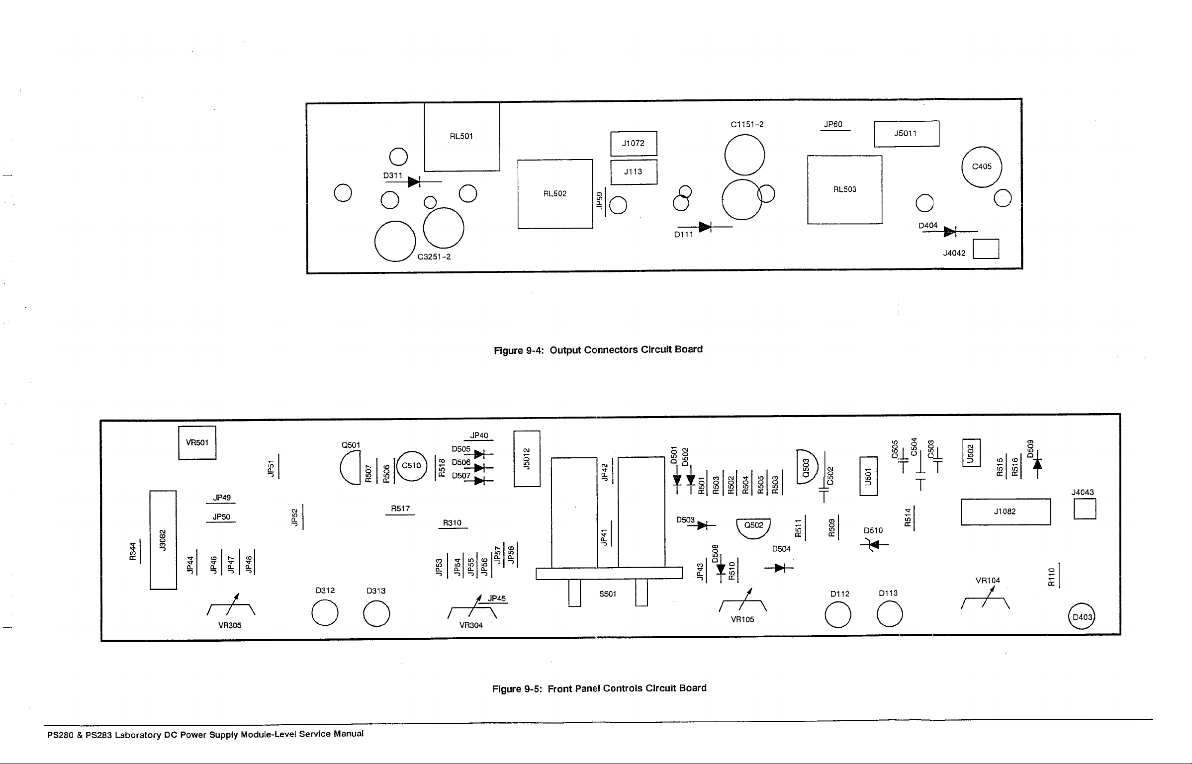
o
O O QO
\ /
C3251-2
8
Figure 9-4: Output Connectors Circuit Board
s
ft
•f-
s s s
o
T
o
1
s
2
I
rv\
o o
PS280 & PS283 Laboratory DC Power Supply Module-Level Service Manual
A
r~r^\
U
- U
Figure 9-5: Front Panel Controls Circuit Board
ll
r^\
/
J1082
4Sh-
/
// \
o o
Page 92

o
O Q3072
o
o
o
J1041
J1042
:
F110
°
no.
0
o
s
o
o
o
o
c
o
o
o
o
o
o
Master
o
P109
P103
P104
J1022 J3022
F102
P105
P107
Pica
J113
J313
o
J3021
o
Figure 9-6: Power Transistors Circuit Boards
PS280 & PS283 Laboratory DC Power Supply Module-Level Service Manual
Figure 9-7: Fuse Circuit Board
Figure 9-8: AC Selector Circuit Board
Page 93

A
2
DVM
P101
a
( TO
JiDi
5
B
JSOO
IS
PART
O
O O S1D3
n?i
6
O O
sia-a
LIN^VOLTASE
SIDE
BOARD
%f%
u
c
J
HUJdd
P
31
GL".
jp
P1033
TO J1O23
512-2 BOARD
TO J3OS3
512-2 BOARD
512-2 BOARD
D
REV AUG 1331
FROM PI13
512-2 BOARD t~
JX
^1
ft
FROM P313
512-2 BOARD ^J
r
AC INPUT. TRANSFORMER
GPC-577 BOARD
TD J1043
PM-515 BOARD
TO J1044
2 , PM-515 BOARD
w REFERENCE DESIGNATORS
&
FUSE BOARD
PARENTHESES ARE SILK SCREENED
ON THE BOARD.
IN
Page 94

P1D1 FROM
MAIN POWER
TRANSFORMER
A
FROM P1023
B
TO FUSE F102
o
GPC-512-1
P3O1 FROM
MAIN POWER
TRANSFORMER
FROM P3O23
D
FROM J1D33 -1
GPC-512-1
I I BPC-S1S-1
REV AUG 133i
MAIN/AUXILIAF:Y RECTIFIER S FILTER
Page 95

A
B
lAf%
D
REV AUS 1991
TO J1DB1
VOLTAGE/CURRENT CONTROL S TRACKING CONTROL
Page 96

A
FROM JSO1H
(RL5O3) *
3i!
(JPSO)
» (RL5O2) x
WSO
KSOS
If3"!
B
FROM P1Q71
FROM PHOS
PM-S15 [20]
FROM PSO7
PM-51S [EDI
FROM J-4O2 v_i I +F
[5C] <^ y2_
(RLSDi) *
^.
iioli
V
u
r
T '#
1
^x
1
^^
1
_2_,
SV FIXED 3A
1 , FROM JiDB
a , [EA] <§>
1 ( FROM J3DB
[BA] <B>
D
REV AUG LSSi
TO P4041
512-5 BOARD
NOTE:
H REFERENCE DESIGNATORS IN
PARENTHESES ARE SILK SCREENED
ON THE BOARD.
OUTPUTS MASTER. SLAVE S 5 VOLT 3 AMP
^>
Page 97

&r%
NOTE: « REFERENCE DESIGNATORS IN
i
REV AUG 1331
PARENTHESES ARE SILK SCREENED
ON THE BOARD.
PARTIA._ 512-1 BO
MASTER VOLTAGE/CURRENT
Page 98

FROM JliOl
A
B
D
REV AUB 1SS1
SLAVE VOLTAGE/CURRENT
Page 99

A
FROM JliDl x A
mm
<|> ^a
5
B
FROM J4O42-1
FROM J4O42-2
g^T^Eo
^ -
I
r
PARTIAL
512-S
BO
+5 VOLT FIXED
Page 100

m:
(0206)
(0208)
*
/LSOIO
/LED11
13
Tg
/LEO1G
10
*
A
B
(VRSO1]
R201
*
RHDS
1
(UNITS)
(MINUS)
10
LE010/
1-4
LE012/
It
2O
LED22/
1
U2112
J
f-J
LED
(O.
.S31
(JPO4)
IS
r
(JP1O4)
(JP1OS)
«
*
7=r
M
TT
(0B03)
mis—Q\
T?
*t
D
FROM
J113
VOLTAGE
ACCURACY
BP/GND
u
PM-S15 PARTIAL CONTROL BOARD
PM-513 PARTIAL DISPLAY BOARD
#
CURRENT
ACCRURACY
FROM
J10B1
REV
AUE 1331
REFERENCE DESIGNATORS
PARENTHESES
ON
THE
ARE
BOARD.
MASTER DIGITAL METER
IN
SILK SCREENED
 Loading...