

Tektronix PCI Express Reference manual
Reference
PCI Express
Methods of Implementation (MOI)
071-1772-00
www.tektronix.com

Copyright © Tektronix, Inc. All rights reserved. Licensed software products are owned by Tektronix or its
suppliers and are protected by United States copyright laws and international treaty provisions.
Tektronix products are covered by U.S. and foreign patents, issued and pending. Information in this publication
supercedes that in all previously published material. Specifications and price change privileges reserved.
TEKTRONIX, TEK and RT-Eye are registered trademarks of Tektronix, Inc.
Contacting Tektronix
Tektronix, Inc.
14200 SW Karl Braun Drive or P.O. Box 500
Beaverton, OR 97077 USA
For product information, sales, service, and technical support:
In North America, call 1-800-833-9200.
Worldwide, visit www.tektronix.com to find contacts in your area.

Table of Contents
1 Introduction to the RT-Eye PCI Express Compliance Module.............1
2 PCI Express Compliance Specifications..................................................2
2.1 Differential Transmitter (TX) Output Specifications............................. 3
2.2 Differential Transmitter (TX) Compliance Eye Diagrams ....................4
2.3 Differential Receiver (RX) Input Specifications ..................................... 5
2.4 Differential Receiver (RX) Compliance Eye Diagrams.......................... 5
2.5 Add-In Card Transmitter Path Compliance Specifications .................. 6
2.6 Add-In Card Compliance Eye Diagrams ................................................7
2.7 System Board Transmitter Path Compliance Eye Diagrams ................ 7
2.8 System Board Compliance Eye Diagrams............................................... 8
2.9 PCI ExpressModule™ Compliance Specifications................................. 9
2.9.1 ExpressModule Add-In Card Transmitter Path
Specifications................................................................................... 9
Table of Contents
2.9.2 ExpressModule System Board Transmitter Path ..........................
Compliance Eye Diagrams ........................................................... 10
2.9.3 Express Module System Board Compliance Eye Diagrams...... 10
2.10 PCI Express External Cabling Specifications....................................... 11
2.10.1 External Cabling Transmitter Path Specifications ................... 11
2.10.2 Cable (Transmitter Side) Eye Diagrams.................................... 11
2.10.3 External Cabling Receiver Path Specifications .........................12
2.10.4 Cable (Receive Side) Eye Diagrams............................................ 12
2.11 Reference Clock Compliance Specifications .........................................13
3 Preparing to Take Measurements..........................................................14
3.1 Required Equipment ............................................................................... 14
3.2 Probing Options for Transmitter Testing .............................................14
3.2.1 SMA Input Connection................................................................. 15
3.2.2 ECB pad connection...................................................................... 16
3.3 Initial Oscilloscope Setup........................................................................ 17
3.4 Running the RT-Eye Software ...............................................................17
3.5 Configuring the Software to take measurements..................................18
3.5.1 Select Standard.............................................................................. 18
3.5.2 Select Test Point ............................................................................18
3.5.3 Select Probe Type.......................................................................... 19
PCI Express i

Table of Contents
4 PCI Express Transmitter Compliance Testing.....................................24
4.1 Probing the link for TX compliance.......................................................24
4.2 TX Compliance Test Load ......................................................................24
4.3 Running a Transmitter (TX) Compliance Test..................................... 24
3.5.4 Select Measurements..................................................................... 19
3.5.5 Configure Source of Waveforms.................................................. 20
3.5.6 Configure Clock Recovery ...........................................................21
3.5.7 Configure Plots .............................................................................. 23
4.3.1 TX Unit Interval Measurement MOI ..........................................26
4.3.2 TX Differential Pk-Pk Output Voltage MOI.............................. 27
4.3.3 TX De-Emphasized Differential Output Voltage (Ratio)
MOI....................................................................................................... 29
4.3.4 Minimum TX Eye Width MOI ....................................................30
4.3.5 TX Median-to-Max Jitter MOI.................................................... 31
4.3.6 TX Output Rise/Fall Time MOI ..................................................32
4.3.7 TX AC Common Mode Output Voltage MOI ............................34
4.3.8 TX Delta DC Common Mode Voltage MOI ...............................35
4.3.9 TX Total Jitter@BER MOI .........................................................36
4.3.10 Spectrum Analysis Based Rj/Dj Separation on ............................
Repeating Pattern ........................................................................36
4.3.11 Arbitrary Pattern Analysis Based Rj/Dj Separation ................38
4.3.12 TX Deterministic MOI (Using Dual-Dirac Model) ...................39
4.3.13 Rj/Dj Separation Based on Dual Dirac Model .......................... 39
4.3.14 TX Waveform Eye Diagram Mask Test MOI ...........................40
5 PCI Express Receiver (RX) Compliance Testing..................................41
5.1 Probing the Link for RX Compliance.................................................... 41
5.2 Running a Complete RX Compliance Test ...........................................41
5.2.1 RX Unit Interval Measurement MOI.......................................... 42
5.2.2 RX Differential Pk-Pk Input Voltage MOI................................. 42
5.2.3 Minimum RX Eye Width MOI .................................................... 43
5.2.4 RX Median-to-Max Jitter MOI ...................................................44
5.2.5 RX Total Jitter@BER MOI ......................................................... 45
5.2.6 RX Deterministic Jitter@BER using Dual-Dirac model ........... 46
5.2.7 RX Waveform Eye Diagram Mask Test MOI ............................47
ii PCI Express

Table of Contents
6 PCI Express Interconnect Test Point Testing .......................................48
6.1 Unit Interval Measurement MOI ........................................................... 49
6.2 Transition and Non-Transition Bit Eye Height Measurement MOI ..49
6.3 Eye Width Measurement MOI ............................................................... 50
6.4 Interconnect Median-to-Max Jitter and Total Jitter@BER MOI ...... 52
7 PCI Express Reference Clock Compliance Measurements .................53
7.1 Probing the Link for Reference Clock Compliance .............................53
7.2 Running a Complete Reference Clock Compliance Test ..................... 53
7.2.1 Reference Clock Frequency Measurement Test MOI ...............54
7.2.2 Reference Clock Differential Voltage Hi and Lo Test MOI...... 55
7.2.3 Reference Clock Differential rise and fall edge rates test MOI 56
7.2.4 Reference clock Duty cycle test MOI........................................... 57
7.2.5 Reference Clock Jitter Test MOI................................................. 58
8 Using SigTest............................................................................................59
9 Using Dynamic Test Points .....................................................................62
9.1 Test Point File Syntax.............................................................................. 63
9.2 Creating the new Test Point ...................................................................65
9.3 Running a test with the new DTP........................................................... 66
10 Giving a Device an ID..............................................................................67
11 Creating a Compliance Report...............................................................67
12 Further Analysis Techniques..................................................................67
13 Ensuring Compliance over specified population ..................................68
PCI Express iii

Table of Contents
iv PCI Express
Methods of Implementation
1 Introduction to the RT-Eye PCI Express Compliance Module1
This document provides the procedures for making PCI Express compliance measurements with Tektronix
TDS6000 Series and TDS7704B, real time oscilloscopes (6 GHz models and above) and probing solutions.
The PCI Express (PCI-E) Compliance Module Version 2.0 (Opt. PCE) is an optional software plug-in to the
RT-Eye Serial Data Compliance and Analysis software (Opt. RTE). The PCI Express Compliance module
provides transmitter path measurements (amplitude, timing, and jitter), waveform mask testing, and
Reference Clock (RefClk) compliance measurements described in multiple variants of the PCI Express
specifications. Specifications covered in this document and the PCE module includes a total of eighteen data
and reference clock test points defined in the following specifications.
Additional test points can also be added by the user, or provided by Tektronix representatives, using
Dynamic Test Point (DTP) definition, described in detail in Section 9.
Table 1 – Supported Specifications
Test Methods Spec
Revision
Rev1.0a
Rev1.1
Rev1.0a Base Specification Transmitter and Receiver
Rev 1.0 Mobile Graphics Lower Power Addendum Transmitter (Section 2.2)
Rev1.0a CEM (Card Electro-Mechanical) Specification System and Add-In Card
Rev1.1 Base Specification Transmitter & Receiver
Rev1.1 CEM Specification System and Add-In Card
Rev1.0 Express Module Specification Transmitter Path and System
Rev0.4C External Cabling Specification Transmitter and Receiver Path
TBD Future 2.5 Gb/s Variants Dynamic Test Points as
PCI Express Specification Title Test Points Defined
(Section 4.3)
(Section 4.7)
(Section 4.3)
(Section 4.7)
Reference Clock (Section 2.1)
Board (Section 5.4)
(Section 3.3)
specifications are defined
Gen2 Rev0.3 Base Specification Transmitter & Receiver
(Section 4.4)
Mobile Low Power Transmitter
(Section 4.4)
Reference Clock (Section 4.4)
1
Disclaimer: The tests provided in the PCI Express compliance module (which are described in this document) do not guarantee PCI Express
compliance. The test results should be considered “Pre-Compliance”. Official PCI Express compliance and PCI-SIG Integrator List qualification
is governed by the PCI-SIG (Special Interest Group) and can be achieved only through official PCI-SIG sanctioned testing.
PCI Express 1

Methods of Implementation
Test Methods Spec
Revision
TBD Future 5 Gb/s Variants Dynamic Test Points as
PCI Express Specification Title Test Points Defined
specifications are defined
Refer to http://www.pcisig.com/specifications/pciexpress/ for the latest specifications.
The PCE module can also be used to automate setup procedures for SigTest by using its SigTest Import
feature (Refer to Section 8).
In this document, for all references to the PCI Express Base Specification and Card Electrical Mechanical
(CEM) specification, refer to all versions of the Spec. (Rev 1.0a, 1.1, and Gen2). Differences between the
specifications are specifically called out when appropriate.
In the subsequent sections, step-by-step procedures are described to help you perform PCI Express
measurements. Each measurement is described as a Method of Implementation (MOI). For further reference,
consult the Compliance checklists offered to PCI-SIG members at www.pcisig.com
.
2 PCI Express Compliance Specifications
As shown in Table 1, Electrical Specifications for PCI Express are provided in multiple documents. This
section provides a summary of the measurement parameters measured in the RT-Eye PCE module and how
they are related to the symbol and test limits in the specification.
2 PCI Express
Methods of Implementation
2.1 Differential Transmitter (TX) Output Specifications
The following table shows the available measurements in the PCE Module and their test limits defined in
each of the Base specifications.
Table 2- Supported base specification transmitter measurements
Specification Parameter Symbol(s)
Gen1
Rev1.0a
Unit interval UI 400 ps
+/- 300 ppm
Differential p-p TX
voltage swing
Low power differential
V
V
TX-SWING
V
TX-SWING-LOW
pDIFFpTX
−−
Not Specfied Not Specfied
0.8 V (min)
1.2 V (max)
p-p TX voltage swing
De-emphasized output
voltage ratio
Transmitter eye
including all jitter
sources
Maximum time
between the jitter
median and maximum
RATIODETXV−−
EYETXT−
t
TX-EYE_TJ
T
TX-EYEMEDIAN-to-MAXJITTER
-3.0 dB (min)
-4.0 dB (max)
.70 UI (min) .75 UI (min) .75 UI (min)
.125 UI (max) .125 UI (max) Not Spec’d
deviation from the
median
Deterministic jitter
T
TX-DJ-DD
0.15 UI (max)
Gen1
Rev1.1
400 ps
+/- 300 ppm
0.8 V (min)
1.2 V (max)
-3.0 dB (min)
-4.0 dB (max)
Gen2
Rev0.3
200 ps
+/- 300 ppm
0.8 V (min)
1.2 V (max)
0.4 V (min)
0.6 V (max)
-5.5 dB (min)
-6.5 dB (max)
D+/D- TX output
rise/fall Time
AC RMS common
mode output voltage
Absolute delta of DC
common mode voltage
between D+ and D-
RISETXT−
V
FALLTXT−
ACpCMTXV−−
DELTALINEDCCMTX
−−−−
0.125 UI (min) 0.125 UI (min) 0.15 UI (min)
20 mV (max) Not Specfied Not Specfied
0 V (min)
25 mV (max)
0 V (min)
25 mV (max)
0 V (min)
25 mV (max)
PCI Express 3
Methods of Implementation
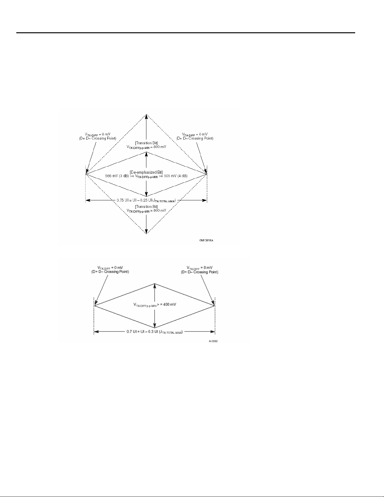
2.2 Differential Transmitter (TX) Compliance Eye Diagrams
Figure 1a shows the eye mask definitions for the Rev1.1 Base specification. It provides an example of a
transmitter mask for a signal with de-emphasis. Transition and non-transition bits must be separated to
perform the mask testing. The amplitude and jitter mask geometries are derived from the amplitude and
jitter specifications. Low power transmitter variants in both Gen1 and Gen2 do not use de-emphasis (This
is shown in Figure 1b).
Figure 1a: Transmitter eye masks for transition and non-transition bits
Figure 1b: Transmitter eye mask for low power variant where de-emphasis is not used
4 PCI Express
Methods of Implementation
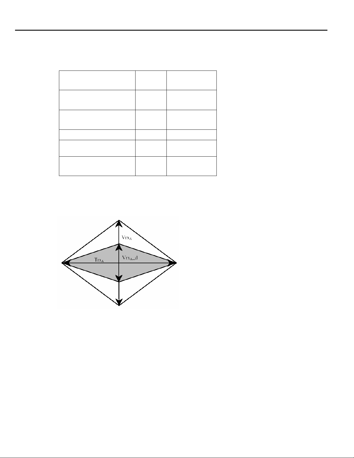
2.3 Differential Receiver (RX) Input Specifications
The following table shows the available measurements in the PCE Module and their test limits defined in
each of the Base specifications.
Table 3 – Supported base specification receiver measurements
Parameter Symbol
Unit interval UI 400 ps
Gen1
Rev1.0a
Gen1
Rev1.1
400 ps
Gen2
Rev0.3
200 ps
Minimum receiver eye height
Minimum receiver eye width
Receiver deterministic jitter –
V
RX_EYE
T
RX_DJ_DD
+/- 300 ppm
.175 V (min)
1.2 V (max)
EYERXT−
.40 UI (min) .40 UI (min) .40 UI (min)
Not Specfied Not Specfied .44 UI (max)
+/- 300 ppm
.175 V (min)
1.2 V (max)
+/- 300 ppm
.120 V (min)
1.2 V (max)
Dj
Maximum time between the
jitter median and maximum
deviation from the median.
T
TX-EYEMEDIAN-to-MAXJITTER
.30 UI (max) .30 UI (max)
Not
Specified
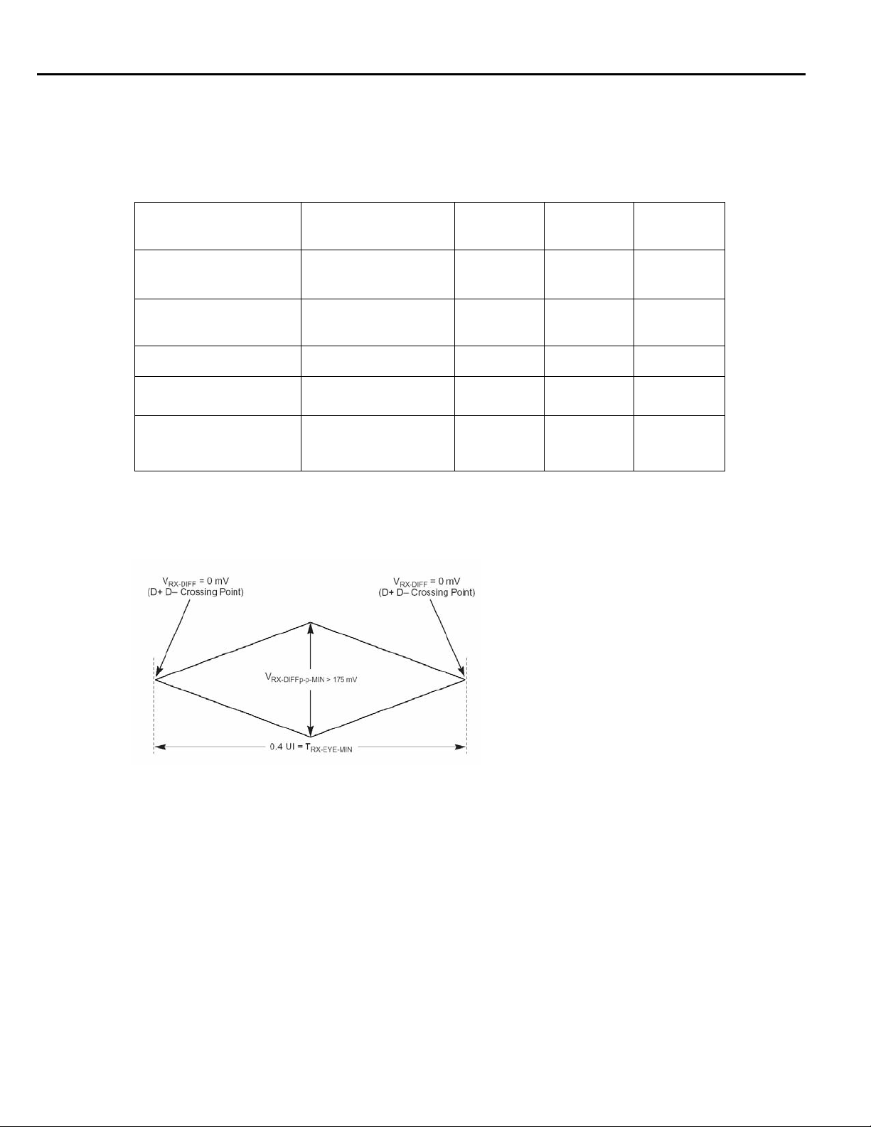
2.4 Differential Receiver (RX) Compliance Eye Diagrams
Figure 2 shows the receiver eye mask definitions for the Rev1.1 Base specification. The amplitude and
jitter mask geometries are derived from the amplitude and jitter specifications.
Figure 2: Receiver input eye mask
PCI Express 5
Methods of Implementation
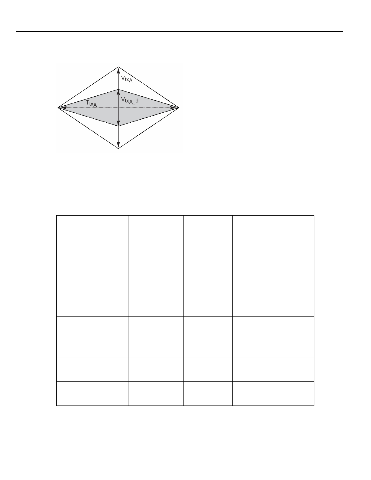
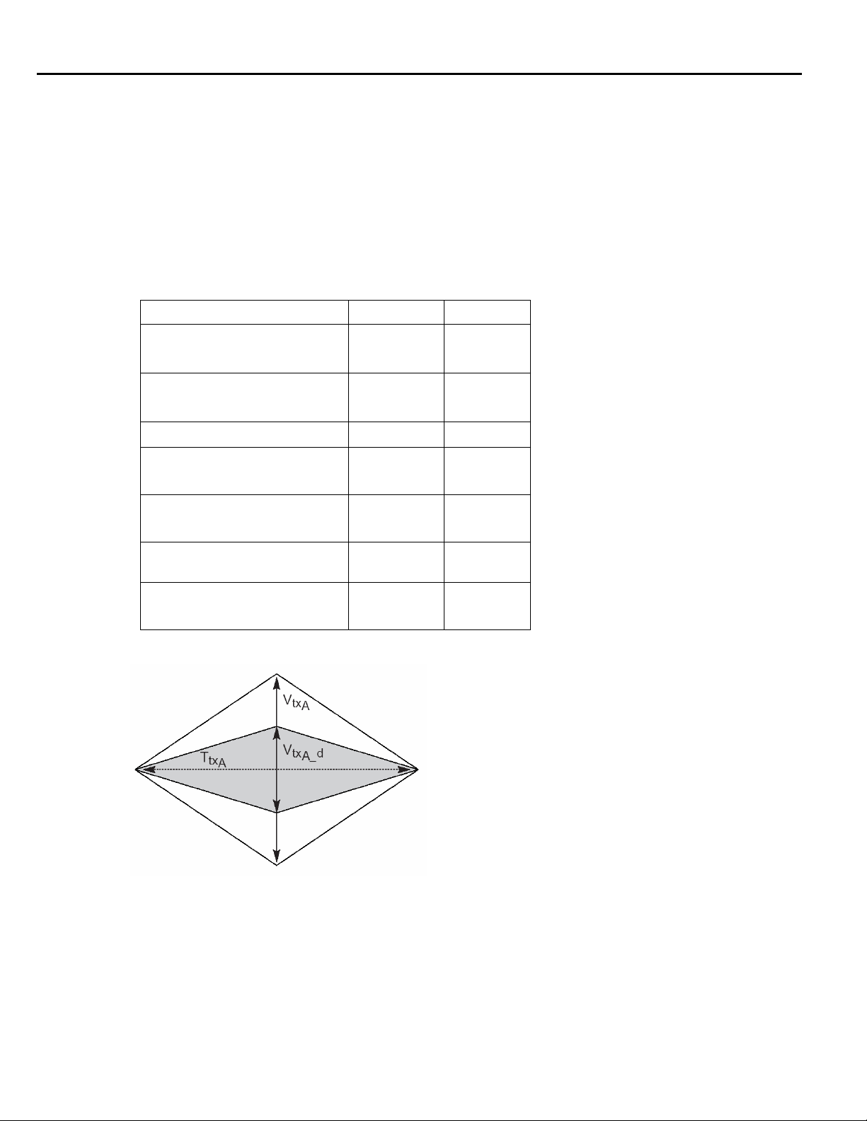
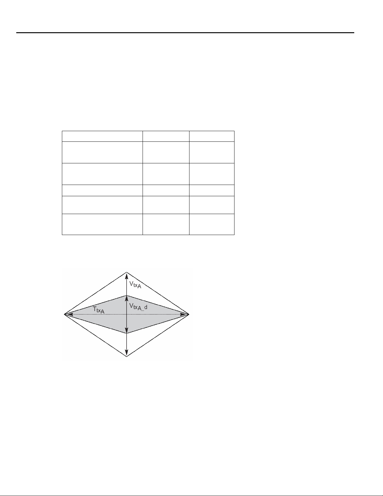
2.5 Add-In Card Transmitter Path Compliance Specifications
Table 5 is derived from the Electrical Mechanical Specifications (CEM). See the CEM Specification for
additional notes and test definitions.
Table 4 – Supported CEM add-in card measurements
Parameter Symbol Gen1
Gen1
Gen2
Rev1.0a
Unit interval UI 400 ps
+/- 300 ppm
V
V
TXA
TXA_d
.514 V (min)
1.2 V (max)
.360 V (min) .360 V (min) TBD
Eye height of transition
bits
Eye height of non-
Rev1.1
400 ps
+/- 300 ppm
.514 V (min)
1.2 V (max)
Rev0.3
200 ps
+/- 300 ppm
TBD
transition bits
T
Eye width across any
250 UIs
Eye width with sample
size of 10
6
UI
Jitter eye opening at
-12
BER 10
Maximum median-max
TXA
In Rev1.0a
T
TXA
In Rev1.1
J
TXA-MEDIAN-to-MAX-JITTER
237 ps (min) Not
Specified
Not Specfied 287 ps (min) TBD
Not Specfied 274 ps (min)
Not Specfied 56.5 ps (max) TBD
TBD
TBD
jitter outlier with sample
size of 10
Maximum median-max
jitter outlier with sample
size of 10
6
6
UI
UI
Not Specfied 63 ps (max)
TBD
6 PCI Express
Methods of Implementation
2.6 Add-In Card Compliance Eye Diagrams
The amplitude and jitter masks are derived from the amplitude and jitter specifications in Table 4.
Figure 3: Add-in card compliance eye masks
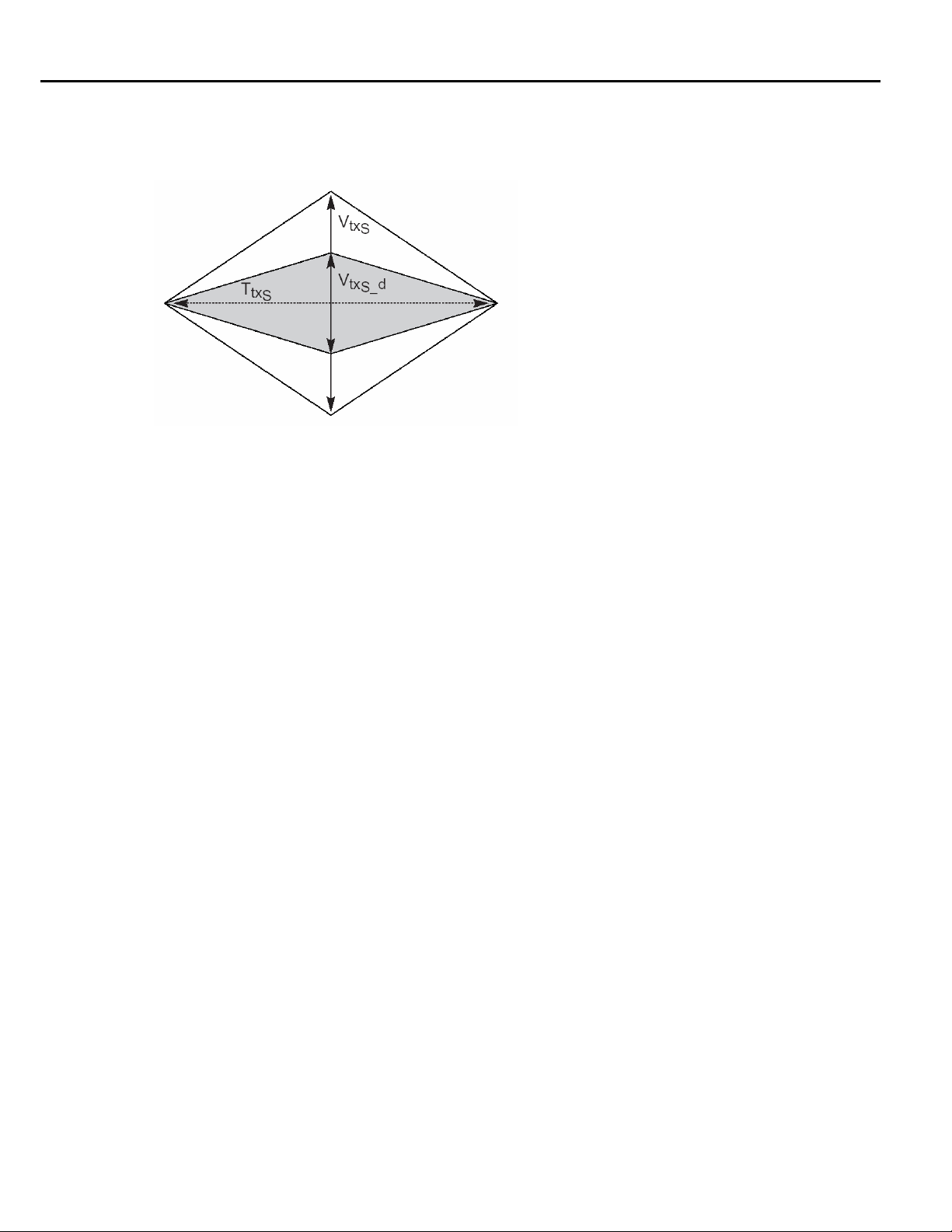
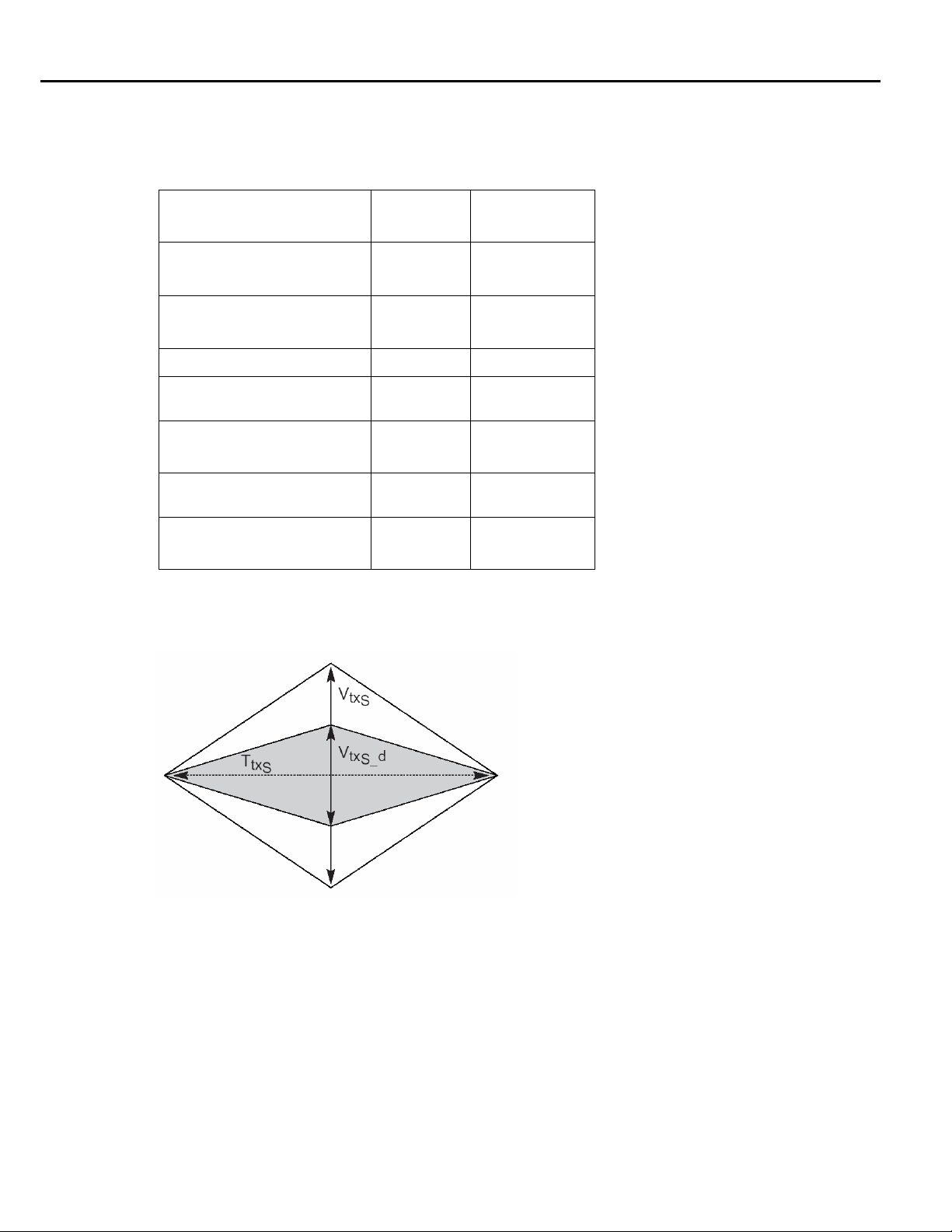
2.7 System Board Transmitter Path Compliance Eye Diagrams
Table 6 is derived from the Electrical Mechanical Specifications (CEM). See the CEM Specification for
additional notes and test definitions.
Table 5 – Supported CEM System Board Measurements
Parameter Symbol Gen1
Gen1
Gen2
Rev1.0a
Unit interval UI 400 ps
+/- 300 ppm
V
Eye height of transition bits
TXS
.274 V (min)
1.2 V (max)
V
Eye height of non-transition
TXS_d
.253 V (min) .253 V (min) TBD
Rev1.1
400 ps
+/- 300 ppm
.274 V (min)
1.2 V (max)
Rev0.3
200 ps
+/- 300 ppm
TBD
bits
T
Eye width across any 250
UIs
Eye width with sample size of
6
10
UI
Jitter eye opening at BER 10
12
Maximum median-max jitter
outlier with sample size of
6
10
UI
Maximum median-max jitter
outlier with sample size of
6
10
UI
-
TXS
18 ps (min) Not Specfied TBD
In Rev1.0a
T
TXS
Not Specfied 246 ps (min) TBD
In Rev1.1
Not Specfied 233 ps (min)
J
TXA-MEDIAN-to-MAX-
JITTER
Not Specfied 77 ps (max) TBD
Not Specfied 83.5 ps (max)
TBD
TBD
PCI Express 7
Methods of Implementation
2.8 System Board Compliance Eye Diagrams
The amplitude and jitter masks are derived from the amplitude and jitter specifications in Table 5.
Figure 4: System Board Compliance Eye Masks
8 PCI Express
Methods of Implementation
2.9 PCI ExpressModule™ Compliance Specifications
The specifications in this section are taken from the PCI Express ExpressModule™ specification, which is
a companion specification to the PCI Express Base specification. Its primary focus is the implementation
of a modular I/O form factor that is focused on the needs of workstations and servers. Measurements in the
PCE module support add-in card and system transmitter path measurements at the PCI Express connector.
2.9.1 ExpressModule Add-In Card Transmitter Path Specifications
Table 6 is derived from Section 5.4.1 of the ExpressModule Electro-Mechanical Specifications Rev. 1.0.
Table 6 – Supported ExpressModule Add-In Card Measurements
Parameter Symbol Rev1.0
Unit interval UI 400 ps
+/- 300 ppm
V
Eye height of transition Bits
Eye height of non-transition Bits
Eye width with sample size of 106 UI
Jitter eye opening at BER 10
-12
Maximum median-max jitter outlier
with sample size of 10
6
UI
Maximum median-max jitter outlier
with sample size of 10
6
UI
TXA
V
TXA_d
T
TXA
In Rev1.1
J
TXA-MEDIAN-to-
MAX-JITTER
.514 V (min)
1.2 V (max)
.360 V (min)
287 ps (min)
274 ps (min)
56.5 ps (max)
63 ps (max)
Figure 5: ExpressModule add-in card compliance eye masks
PCI Express 9
Methods of Implementation
2.9.2 ExpressModule System Board Transmitter Path Compliance Eye Diagrams
Table 7 is derived from Section 5.4.3 of the ExpressModule Electro-Mechanical Specifications Rev. 1.0.
Table 7 – Supported ExpressModule system board measurements
Parameter Symbol Gen1
Unit interval UI 400 ps
Eye height of transition bits
Eye height of non-transition bits
Eye width with sample size of 106
UI
Jitter eye opening at BER 10
Maximum median-max jitter outlier
with sample size of 10
Maximum median-max jitter outlier
with sample size of 10
6
6
V
TXS
V
TXS_d
T
246 ps (min)
TXS
-12
233 ps (min)
J
TXA-MEDIAN-
UI
to-MAX-JITTER
UI
Rev1.0
+/- 300 ppm
.274 V (min)
1.2 V (max)
.253 V (min)
77 ps (max)
83.5 ps (max)
2.9.3 Express Module System Board Compliance Eye Diagrams
The amplitude and jitter masks are derived from the amplitude and jitter specifications in Table 7.
Figure 6: ExpressModule system board compliance eye masks
10 PCI Express
Methods of Implementation
2.10 PCI Express External Cabling Specifications
The specifications in this section are taken from the PCI Express External Cabling Specification. Its
primary focus is the implementation of a cabled interconnect. Measurements in the PCE module support
transmitter path and receiver path measurements. These measurements represent the test points at the
transmitter end of the cable and the receiver end of the cable respectively.
2.10.1 External Cabling Transmitter Path Specifications
Table 8 is derived from Section 3.3.1 of the External Cabling Specification Rev. 0.4C.
Table 8 – Supported external cabling transmitter path measurements
Parameter Symbol Rev0.4C
Unit interval UI 400 ps
+/- 300 ppm
V
V
T
TXA
TXA_d
TXA
.659 V (min)
1.2 V (max)
.456 V (min)
309 ps (min)
296 ps (min)
Eye height of transition bits
Eye height of non-transition bits
Eye width with sample size of
6
10
UI
Jitter eye opening at BER 10
-12
2.10.2 Cable (Transmitter Side) Eye Diagrams
The amplitude and jitter masks are derived from the amplitude and jitter specifications in Table 8.
Figure 7: Cable (transmitter side) compliance eye masks
PCI Express 11
Methods of Implementation
2.10.3 External Cabling Receiver Path Specifications
Table 9 is derived from Section 3.3.2 of the External Cabling Specification Rev. 0.4C.
Table 9 – Supported CEM System Board Measurements
Parameter Symbol Gen1
Unit interval UI 400 ps
Eye height of transition bits
Eye height of non-transition bits
Eye width with sample size of 106
UI
Jitter eye opening at BER 10
2.10.4 Cable (Receive Side) Eye Diagrams
Rev1.0
+/- 300 ppm
V
RXA
.219 V (min)
1.2 V (max)
V
RXA_d
T
247 ps (min)
RXA
-12
234 ps (min)
.200 V (min)
The amplitude and jitter masks are derived from the amplitude and jitter specifications in Table 9.
Figure 8: Cable (receiver side) compliance eye masks
12 PCI Express
Methods of Implementation
2.11 Reference Clock Compliance Specifications
Table 10 is derived from section 2.1 of the Gen1 Rev1.1 Electrical Mechanical Specifications (CEM) and
Gen2 Base specifications.
Table 10 – Supported reference clock measurements
Parameter Symbol Gen1
Rev1.1
Rise edge rate
Rise Edge Rate
0.6 V/ns (min)
4.0 V/ns (max)
Fall edge rate
Fall Edge Rate 0.6 V/ns (min)
4.0 V/ns (max)
Differential input high voltage
V
IH
150 mV (max) 150 mV (max)
Differential input low voltage VIL -150 mV (min) -150 mV (min)
Absolute period (including jitter
and spread spectrum)
T
PERIOD_ABS
9.847 ns (min)
10.203 ns (max)
Duty cycle Duty Cycle 40% (min)
60% (max)
Maximum peak-peak filtered
Jitter @ 10
-12
BER 108 ps (max) Not
phase jitter
Gen2
Rev0.3
0.6 V/ns (min)
4.0 V/ns (max)
0.6 V/ns (min)
4.0 V/ns (max)
9.997 ns (min)
10.053 ns (max)
40% (min)
60% (max)
Specified
Maximum peak-peak filtered
phase jitter
RMS jitter T
Jitter @ 10-6 BER 86 ps (max) Not
Specified
3.1 ps (max)
CLK_RJ
PCI Express 13
Methods of Implementation
3 Preparing to Take Measurements
3.1 Required Equipment
The following equipment is required to take the measurements:
• Oscilloscope Selection:
ο Gen1 (2.5 Gb/s) – The PCI-SIG recommends a minimum of 6 GHz system BW for Gen1
Measurements. Tektronix models that meet this recommendation are: All the TDS6000B/C Series
instruments and the TDS7704B.
ο Gen2 (5 Gb/s) – It is recommended that >12 GHz system BW is used for Gen2. This ensures the
th
5
harmonic is represented in the measurements. Tektronix models that meet this
recommendation are TDS6000C models.
• RT-Eye software (Opt. RTE) and PCI Express Compliance Module (PCE) installed.
• Probes – probing configuration is MOI specific. Refer to each MOI for proper probe configuration.
• Test fixture breakout from transmitter to differential SMA connectors. A Compliance Base Board
(CBB) used for add-in card compliance tests and a Compliance Load Board (CLB) used for system
compliance tests are available through the PCI-SIG at the following URL:
http://www.pcisig.com/specifications/ordering_information/ordering_information
• Test fixtures for notebook testing are available from the following URL:
http://www.expresscard.org/web/site/testtools.jsp
3.2 Probing Options for Transmitter Testing
The first step is to probe the link. Use one of the following four methods to connect probes to the link.
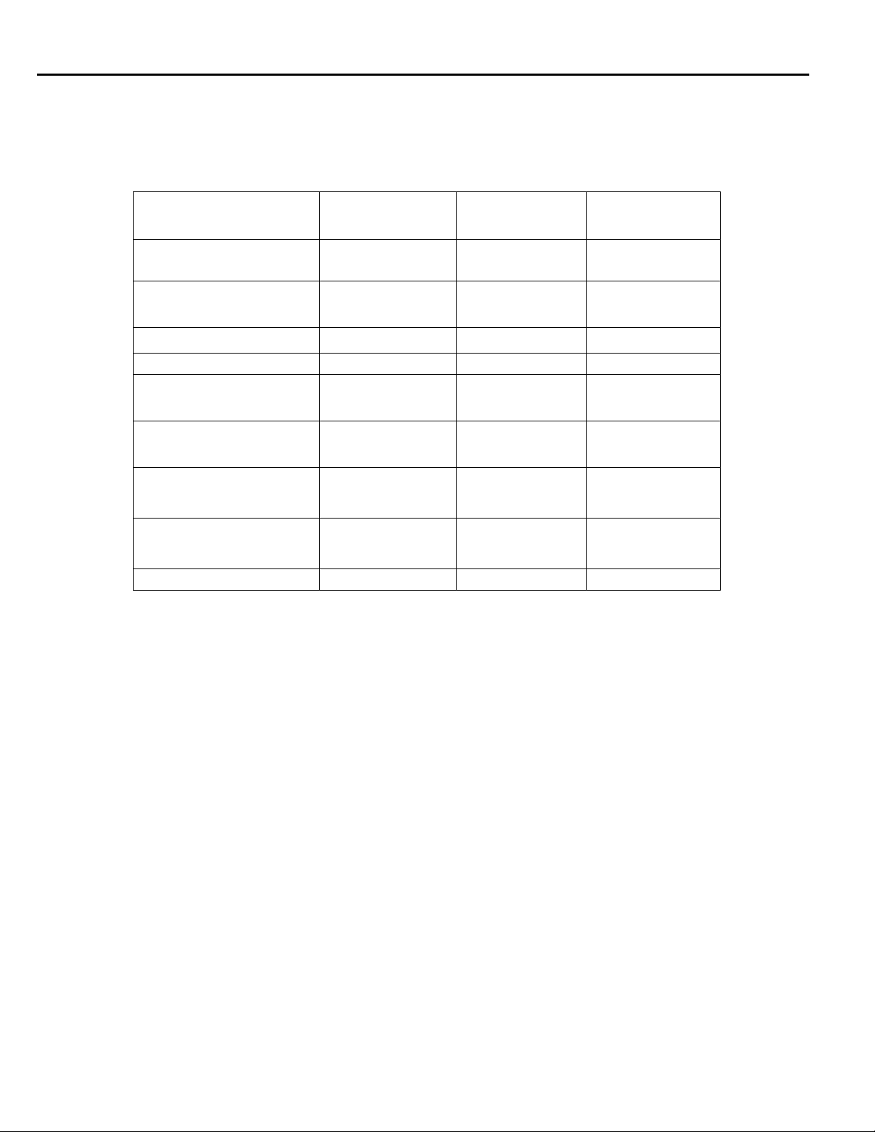
Table 11 – Probing configurations for a PCI express link
14 PCI Express
Methods of Implementation
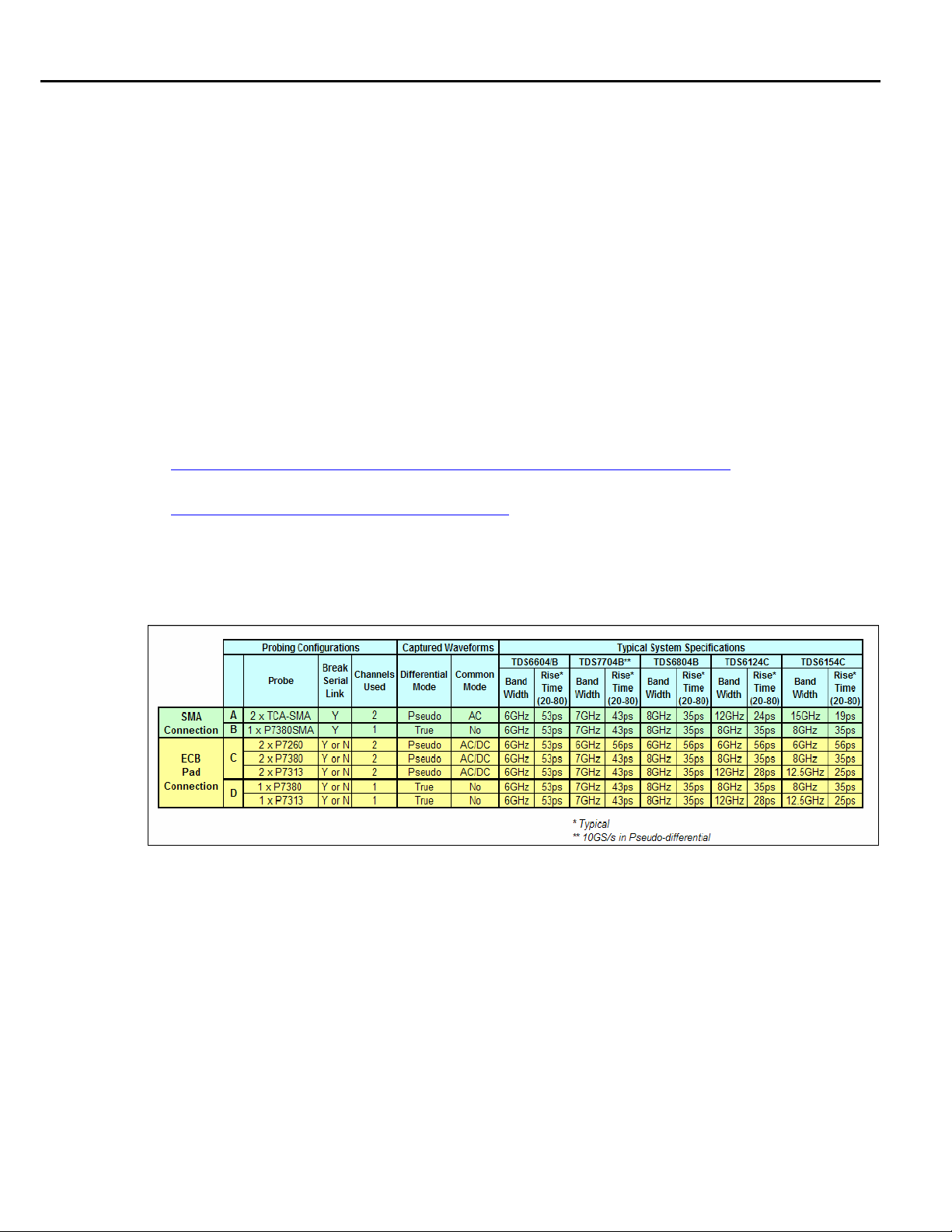
3.2.1 SMA Input Connection
1. Two TCA-SMA inputs using SMA
cables (Ch1) and (Ch3)
The differential signal is created by
the RT-Eye software from the math
waveform Ch1-Ch3. The Common
mode AC measurement is also
available in this configuration from
the common mode waveform
(Ch1+Ch3)/2. This probing technique
requires breaking the link and
terminating into a 50 Ω/side
termination of the oscilloscope.
While in this mode, the PCI Express
SerDes will transmit the compliance
test pattern. Ch-Ch de-skew is
required using this technique because
two channels are used. This
configuration does not compensate
for cable loss in the SMA cables. The
measurement reference plane is at the
input of the TCA-SMA connectors
on the oscilloscope. Any cable loss
should be measured and entered into
the vertical attenuation menu for
accurate measurements at the SMA
cable attachment point.
Probe Configuration A
SMA Psuedo-differential
2. One P7380SMA differential active
probe (Ch1)
The differential signal is measured
across the termination resistors inside
the P7380SMA probe. This probing
technique requires breaking the link.
While in this mode, the PCI Express
SerDes will transmit the compliance
test pattern. Matched cables are
provided with the P7380 probe to
avoid introducing de-skew into the
system. Only one channel of the
oscilloscope is used. The P7380SMA
provides a calibrated system at the
Probe Configuration B
SMA Input Differential Probe
Test Fixture attachment point,
eliminating the need to compensate
for cable loss associated with the
probe configuration A.
PCI Express 15
Methods of Implementation
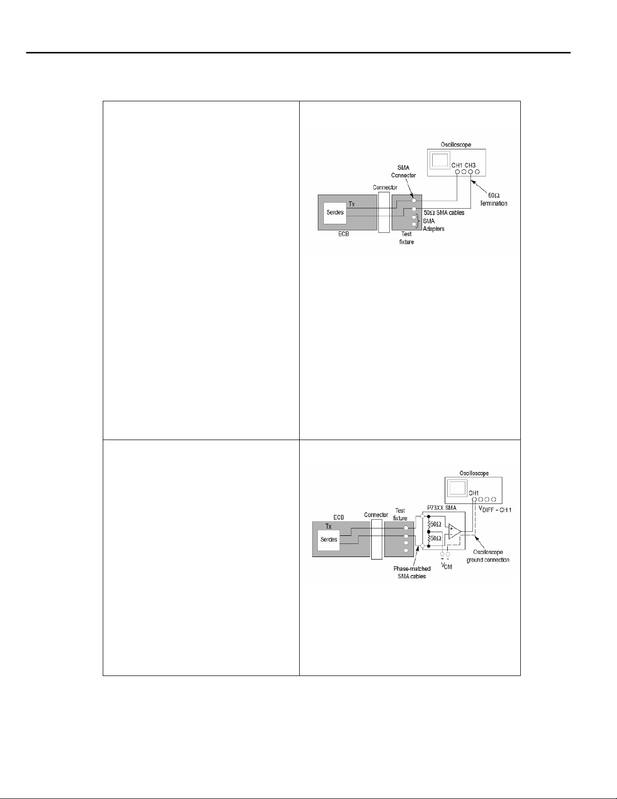
3.2.2 ECB pad connection
3. Two P7300 or P7260 active probes
(Ch1) and (Ch3)
The differential signal is created by the
RT-Eye software from the math
waveform Ch1-Ch3. The Common mode
AC measurement is also available in this
configuration from the common mode
waveform (Ch1+Ch3)/2. This probing
technique can be used for either a live
link that is transmitting data, or a link that
has terminated into a “dummy load.” In
both cases, the single-ended signals
should be probed as close as possible to
the termination resistors on both sides
with the shortest ground connection
possible. Ch-Ch de-skew is required
using this technique because two
channels are used.
Probe Configuration C
Two Single-Ended Active Probes
4. One P7380 Differential probe (Ch1)
The differential signal is measured
directly across the termination resistors.
This probing technique can be used for
either a live link that is transmitting data,
or a link that is terminated into a “dummy
load.” In both cases, the signals should be
probed as close as possible to the
termination resistors. De-skew is not
necessary because a single channel of the
oscilloscope is used.
Probe Configuration D
One Differential Active Probe
16 PCI Express

Methods of Implementation
3.3 Initial Oscilloscope Setup
After connecting the DUT by following the proper probing configuration for the test, click DEFAULT
SETUP and then Autoset to display the serial data bit stream.
3.4 Running the RT-Eye Software
1. On non-B or non-C model oscilloscopes (Example: TDS6604), Go to File > Run Application > RT-
Eye Serial Compliance and Analysis. For B and C models (Example: TDS7704B, TDS6154C), go to
App > RT-Eye Serial Compliance and Analysis.
Figure 9: Default menu of the RT-Eye software
Figure 9 shows the oscilloscope display. The default mode of the software is the Serial Analysis module
(Opt.RTE). This software is intended for generalized Serial Data analysis on 8B/10B encoded copper
links.
2. Select the PCI Express Compliance Module from the Modules pull-down list.
Figure 10: Choosing PCI Express Compliance Module.
PCI Express 17
 Loading...