

Page 1
Reference
PCI Express
Methods of Implementation (MOI)
071-1772-00
www.tektronix.com
Page 2

Copyright © Tektronix, Inc. All rights reserved. Licensed software products are owned by Tektronix or its
suppliers and are protected by United States copyright laws and international treaty provisions.
Tektronix products are covered by U.S. and foreign patents, issued and pending. Information in this publication
supercedes that in all previously published material. Specifications and price change privileges reserved.
TEKTRONIX, TEK and RT-Eye are registered trademarks of Tektronix, Inc.
Contacting Tektronix
Tektronix, Inc.
14200 SW Karl Braun Drive or P.O. Box 500
Beaverton, OR 97077 USA
For product information, sales, service, and technical support:
In North America, call 1-800-833-9200.
Worldwide, visit www.tektronix.com to find contacts in your area.
Page 3

Table of Contents
1 Introduction to the RT-Eye PCI Express Compliance Module.............1
2 PCI Express Compliance Specifications..................................................2
2.1 Differential Transmitter (TX) Output Specifications............................. 3
2.2 Differential Transmitter (TX) Compliance Eye Diagrams ....................4
2.3 Differential Receiver (RX) Input Specifications ..................................... 5
2.4 Differential Receiver (RX) Compliance Eye Diagrams.......................... 5
2.5 Add-In Card Transmitter Path Compliance Specifications .................. 6
2.6 Add-In Card Compliance Eye Diagrams ................................................7
2.7 System Board Transmitter Path Compliance Eye Diagrams ................ 7
2.8 System Board Compliance Eye Diagrams............................................... 8
2.9 PCI ExpressModule™ Compliance Specifications................................. 9
2.9.1 ExpressModule Add-In Card Transmitter Path
Specifications................................................................................... 9
Table of Contents
2.9.2 ExpressModule System Board Transmitter Path ..........................
Compliance Eye Diagrams ........................................................... 10
2.9.3 Express Module System Board Compliance Eye Diagrams...... 10
2.10 PCI Express External Cabling Specifications....................................... 11
2.10.1 External Cabling Transmitter Path Specifications ................... 11
2.10.2 Cable (Transmitter Side) Eye Diagrams.................................... 11
2.10.3 External Cabling Receiver Path Specifications .........................12
2.10.4 Cable (Receive Side) Eye Diagrams............................................ 12
2.11 Reference Clock Compliance Specifications .........................................13
3 Preparing to Take Measurements..........................................................14
3.1 Required Equipment ............................................................................... 14
3.2 Probing Options for Transmitter Testing .............................................14
3.2.1 SMA Input Connection................................................................. 15
3.2.2 ECB pad connection...................................................................... 16
3.3 Initial Oscilloscope Setup........................................................................ 17
3.4 Running the RT-Eye Software ...............................................................17
3.5 Configuring the Software to take measurements..................................18
3.5.1 Select Standard.............................................................................. 18
3.5.2 Select Test Point ............................................................................18
3.5.3 Select Probe Type.......................................................................... 19
PCI Express i
Page 4

Table of Contents
4 PCI Express Transmitter Compliance Testing.....................................24
4.1 Probing the link for TX compliance.......................................................24
4.2 TX Compliance Test Load ......................................................................24
4.3 Running a Transmitter (TX) Compliance Test..................................... 24
3.5.4 Select Measurements..................................................................... 19
3.5.5 Configure Source of Waveforms.................................................. 20
3.5.6 Configure Clock Recovery ...........................................................21
3.5.7 Configure Plots .............................................................................. 23
4.3.1 TX Unit Interval Measurement MOI ..........................................26
4.3.2 TX Differential Pk-Pk Output Voltage MOI.............................. 27
4.3.3 TX De-Emphasized Differential Output Voltage (Ratio)
MOI....................................................................................................... 29
4.3.4 Minimum TX Eye Width MOI ....................................................30
4.3.5 TX Median-to-Max Jitter MOI.................................................... 31
4.3.6 TX Output Rise/Fall Time MOI ..................................................32
4.3.7 TX AC Common Mode Output Voltage MOI ............................34
4.3.8 TX Delta DC Common Mode Voltage MOI ...............................35
4.3.9 TX Total Jitter@BER MOI .........................................................36
4.3.10 Spectrum Analysis Based Rj/Dj Separation on ............................
Repeating Pattern ........................................................................36
4.3.11 Arbitrary Pattern Analysis Based Rj/Dj Separation ................38
4.3.12 TX Deterministic MOI (Using Dual-Dirac Model) ...................39
4.3.13 Rj/Dj Separation Based on Dual Dirac Model .......................... 39
4.3.14 TX Waveform Eye Diagram Mask Test MOI ...........................40
5 PCI Express Receiver (RX) Compliance Testing..................................41
5.1 Probing the Link for RX Compliance.................................................... 41
5.2 Running a Complete RX Compliance Test ...........................................41
5.2.1 RX Unit Interval Measurement MOI.......................................... 42
5.2.2 RX Differential Pk-Pk Input Voltage MOI................................. 42
5.2.3 Minimum RX Eye Width MOI .................................................... 43
5.2.4 RX Median-to-Max Jitter MOI ...................................................44
5.2.5 RX Total Jitter@BER MOI ......................................................... 45
5.2.6 RX Deterministic Jitter@BER using Dual-Dirac model ........... 46
5.2.7 RX Waveform Eye Diagram Mask Test MOI ............................47
ii PCI Express
Page 5

Table of Contents
6 PCI Express Interconnect Test Point Testing .......................................48
6.1 Unit Interval Measurement MOI ........................................................... 49
6.2 Transition and Non-Transition Bit Eye Height Measurement MOI ..49
6.3 Eye Width Measurement MOI ............................................................... 50
6.4 Interconnect Median-to-Max Jitter and Total Jitter@BER MOI ...... 52
7 PCI Express Reference Clock Compliance Measurements .................53
7.1 Probing the Link for Reference Clock Compliance .............................53
7.2 Running a Complete Reference Clock Compliance Test ..................... 53
7.2.1 Reference Clock Frequency Measurement Test MOI ...............54
7.2.2 Reference Clock Differential Voltage Hi and Lo Test MOI...... 55
7.2.3 Reference Clock Differential rise and fall edge rates test MOI 56
7.2.4 Reference clock Duty cycle test MOI........................................... 57
7.2.5 Reference Clock Jitter Test MOI................................................. 58
8 Using SigTest............................................................................................59
9 Using Dynamic Test Points .....................................................................62
9.1 Test Point File Syntax.............................................................................. 63
9.2 Creating the new Test Point ...................................................................65
9.3 Running a test with the new DTP........................................................... 66
10 Giving a Device an ID..............................................................................67
11 Creating a Compliance Report...............................................................67
12 Further Analysis Techniques..................................................................67
13 Ensuring Compliance over specified population ..................................68
PCI Express iii
Page 6

Table of Contents
iv PCI Express
Page 7
Methods of Implementation
1 Introduction to the RT-Eye PCI Express Compliance Module1
This document provides the procedures for making PCI Express compliance measurements with Tektronix
TDS6000 Series and TDS7704B, real time oscilloscopes (6 GHz models and above) and probing solutions.
The PCI Express (PCI-E) Compliance Module Version 2.0 (Opt. PCE) is an optional software plug-in to the
RT-Eye Serial Data Compliance and Analysis software (Opt. RTE). The PCI Express Compliance module
provides transmitter path measurements (amplitude, timing, and jitter), waveform mask testing, and
Reference Clock (RefClk) compliance measurements described in multiple variants of the PCI Express
specifications. Specifications covered in this document and the PCE module includes a total of eighteen data
and reference clock test points defined in the following specifications.
Additional test points can also be added by the user, or provided by Tektronix representatives, using
Dynamic Test Point (DTP) definition, described in detail in Section 9.
Table 1 – Supported Specifications
Test Methods Spec
Revision
Rev1.0a
Rev1.1
Rev1.0a Base Specification Transmitter and Receiver
Rev 1.0 Mobile Graphics Lower Power Addendum Transmitter (Section 2.2)
Rev1.0a CEM (Card Electro-Mechanical) Specification System and Add-In Card
Rev1.1 Base Specification Transmitter & Receiver
Rev1.1 CEM Specification System and Add-In Card
Rev1.0 Express Module Specification Transmitter Path and System
Rev0.4C External Cabling Specification Transmitter and Receiver Path
TBD Future 2.5 Gb/s Variants Dynamic Test Points as
PCI Express Specification Title Test Points Defined
(Section 4.3)
(Section 4.7)
(Section 4.3)
(Section 4.7)
Reference Clock (Section 2.1)
Board (Section 5.4)
(Section 3.3)
specifications are defined
Gen2 Rev0.3 Base Specification Transmitter & Receiver
(Section 4.4)
Mobile Low Power Transmitter
(Section 4.4)
Reference Clock (Section 4.4)
1
Disclaimer: The tests provided in the PCI Express compliance module (which are described in this document) do not guarantee PCI Express
compliance. The test results should be considered “Pre-Compliance”. Official PCI Express compliance and PCI-SIG Integrator List qualification
is governed by the PCI-SIG (Special Interest Group) and can be achieved only through official PCI-SIG sanctioned testing.
PCI Express 1
Page 8
Methods of Implementation
Test Methods Spec
Revision
TBD Future 5 Gb/s Variants Dynamic Test Points as
PCI Express Specification Title Test Points Defined
specifications are defined
Refer to http://www.pcisig.com/specifications/pciexpress/ for the latest specifications.
The PCE module can also be used to automate setup procedures for SigTest by using its SigTest Import
feature (Refer to Section 8).
In this document, for all references to the PCI Express Base Specification and Card Electrical Mechanical
(CEM) specification, refer to all versions of the Spec. (Rev 1.0a, 1.1, and Gen2). Differences between the
specifications are specifically called out when appropriate.
In the subsequent sections, step-by-step procedures are described to help you perform PCI Express
measurements. Each measurement is described as a Method of Implementation (MOI). For further reference,
consult the Compliance checklists offered to PCI-SIG members at www.pcisig.com
.
2 PCI Express Compliance Specifications
As shown in Table 1, Electrical Specifications for PCI Express are provided in multiple documents. This
section provides a summary of the measurement parameters measured in the RT-Eye PCE module and how
they are related to the symbol and test limits in the specification.
2 PCI Express
Page 9
Methods of Implementation
2.1 Differential Transmitter (TX) Output Specifications
The following table shows the available measurements in the PCE Module and their test limits defined in
each of the Base specifications.
Table 2- Supported base specification transmitter measurements
Specification Parameter Symbol(s)
Gen1
Rev1.0a
Unit interval UI 400 ps
+/- 300 ppm
Differential p-p TX
voltage swing
Low power differential
V
V
TX-SWING
V
TX-SWING-LOW
pDIFFpTX
−−
Not Specfied Not Specfied
0.8 V (min)
1.2 V (max)
p-p TX voltage swing
De-emphasized output
voltage ratio
Transmitter eye
including all jitter
sources
Maximum time
between the jitter
median and maximum
RATIODETXV−−
EYETXT−
t
TX-EYE_TJ
T
TX-EYEMEDIAN-to-MAXJITTER
-3.0 dB (min)
-4.0 dB (max)
.70 UI (min) .75 UI (min) .75 UI (min)
.125 UI (max) .125 UI (max) Not Spec’d
deviation from the
median
Deterministic jitter
T
TX-DJ-DD
0.15 UI (max)
Gen1
Rev1.1
400 ps
+/- 300 ppm
0.8 V (min)
1.2 V (max)
-3.0 dB (min)
-4.0 dB (max)
Gen2
Rev0.3
200 ps
+/- 300 ppm
0.8 V (min)
1.2 V (max)
0.4 V (min)
0.6 V (max)
-5.5 dB (min)
-6.5 dB (max)
D+/D- TX output
rise/fall Time
AC RMS common
mode output voltage
Absolute delta of DC
common mode voltage
between D+ and D-
RISETXT−
V
FALLTXT−
ACpCMTXV−−
DELTALINEDCCMTX
−−−−
0.125 UI (min) 0.125 UI (min) 0.15 UI (min)
20 mV (max) Not Specfied Not Specfied
0 V (min)
25 mV (max)
0 V (min)
25 mV (max)
0 V (min)
25 mV (max)
PCI Express 3
Page 10
Methods of Implementation
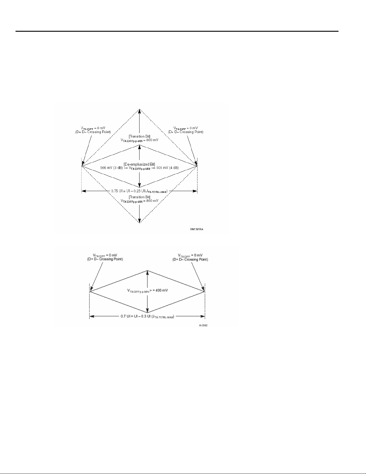
2.2 Differential Transmitter (TX) Compliance Eye Diagrams
Figure 1a shows the eye mask definitions for the Rev1.1 Base specification. It provides an example of a
transmitter mask for a signal with de-emphasis. Transition and non-transition bits must be separated to
perform the mask testing. The amplitude and jitter mask geometries are derived from the amplitude and
jitter specifications. Low power transmitter variants in both Gen1 and Gen2 do not use de-emphasis (This
is shown in Figure 1b).
Figure 1a: Transmitter eye masks for transition and non-transition bits
Figure 1b: Transmitter eye mask for low power variant where de-emphasis is not used
4 PCI Express
Page 11
Methods of Implementation
2.3 Differential Receiver (RX) Input Specifications
The following table shows the available measurements in the PCE Module and their test limits defined in
each of the Base specifications.
Table 3 – Supported base specification receiver measurements
Parameter Symbol
Unit interval UI 400 ps
Gen1
Rev1.0a
Gen1
Rev1.1
400 ps
Gen2
Rev0.3
200 ps
Minimum receiver eye height
Minimum receiver eye width
Receiver deterministic jitter –
V
RX_EYE
T
RX_DJ_DD
+/- 300 ppm
.175 V (min)
1.2 V (max)
EYERXT−
.40 UI (min) .40 UI (min) .40 UI (min)
Not Specfied Not Specfied .44 UI (max)
+/- 300 ppm
.175 V (min)
1.2 V (max)
+/- 300 ppm
.120 V (min)
1.2 V (max)
Dj
Maximum time between the
jitter median and maximum
deviation from the median.
T
TX-EYEMEDIAN-to-MAXJITTER
.30 UI (max) .30 UI (max)
Not
Specified
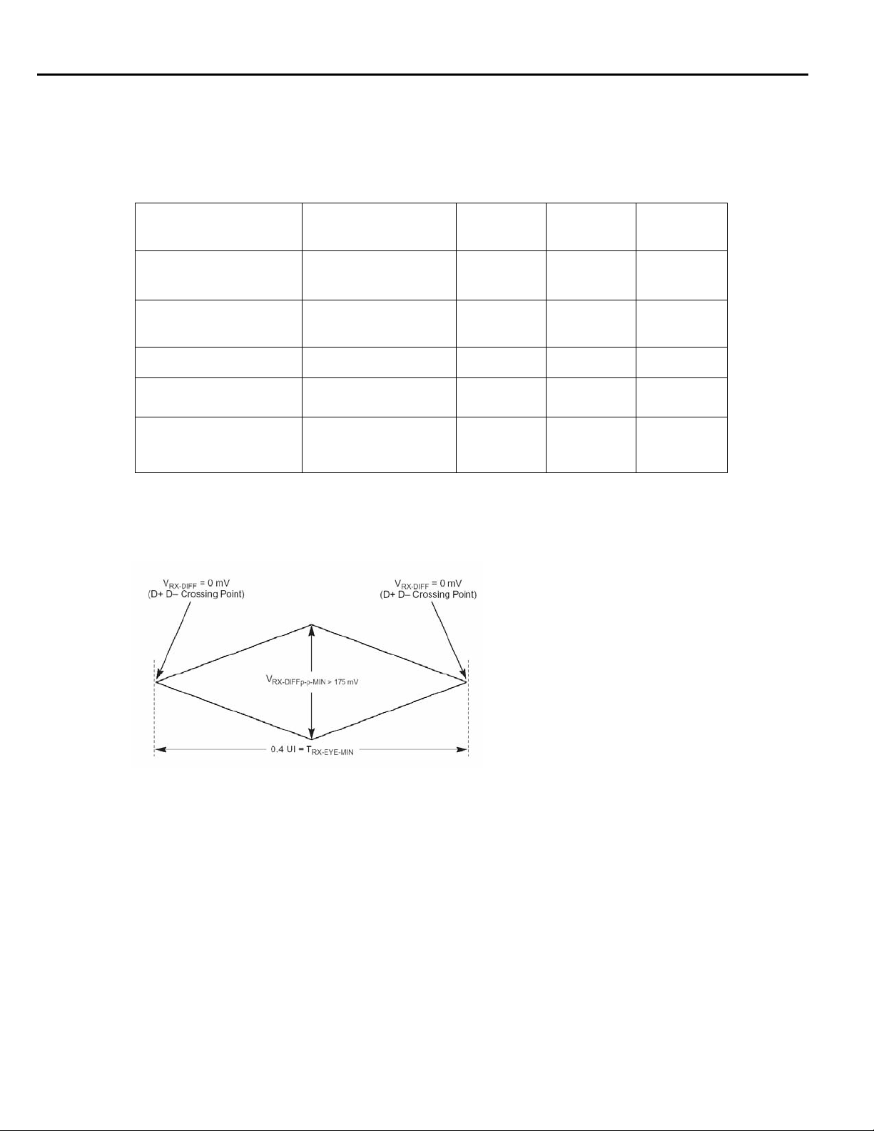
2.4 Differential Receiver (RX) Compliance Eye Diagrams
Figure 2 shows the receiver eye mask definitions for the Rev1.1 Base specification. The amplitude and
jitter mask geometries are derived from the amplitude and jitter specifications.
Figure 2: Receiver input eye mask
PCI Express 5
Page 12
Methods of Implementation
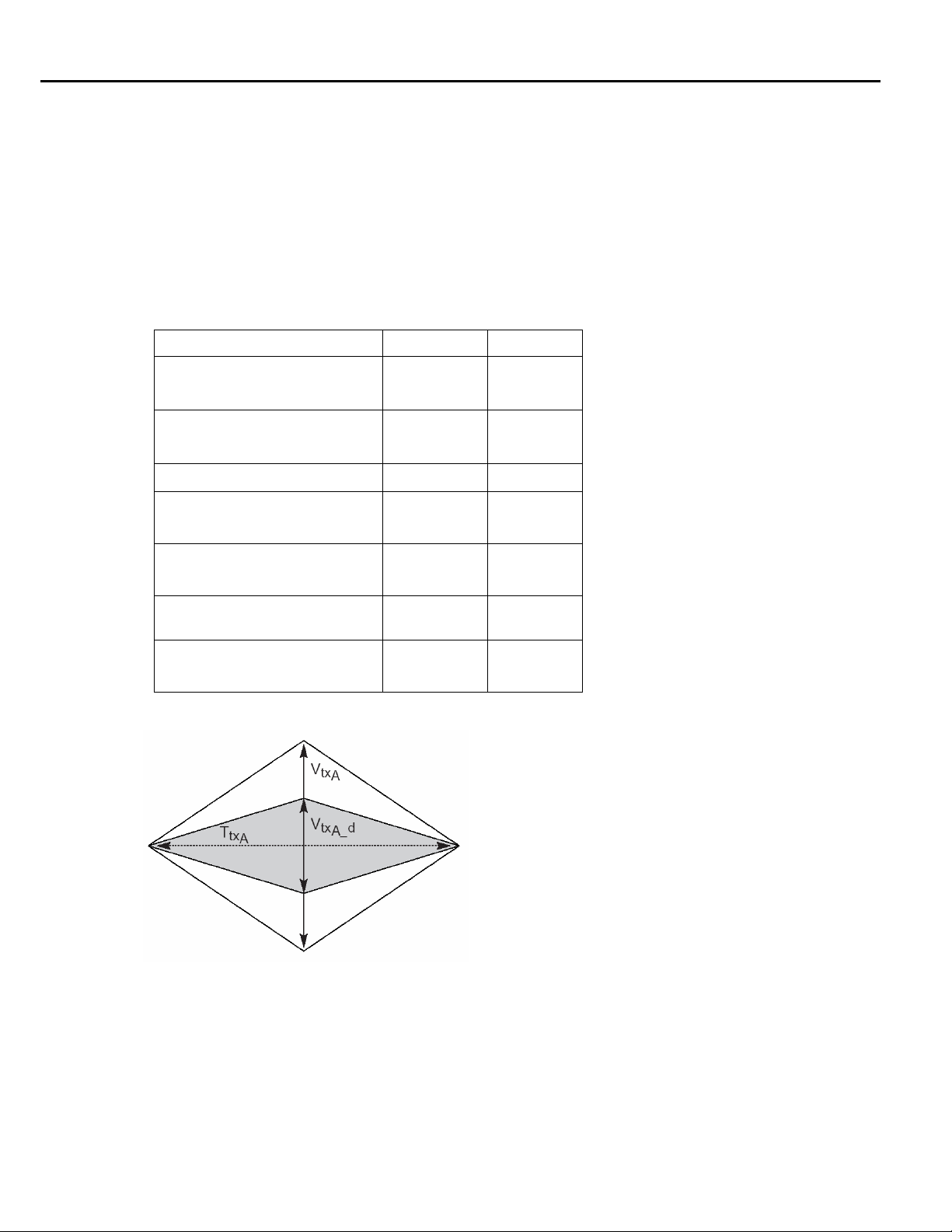
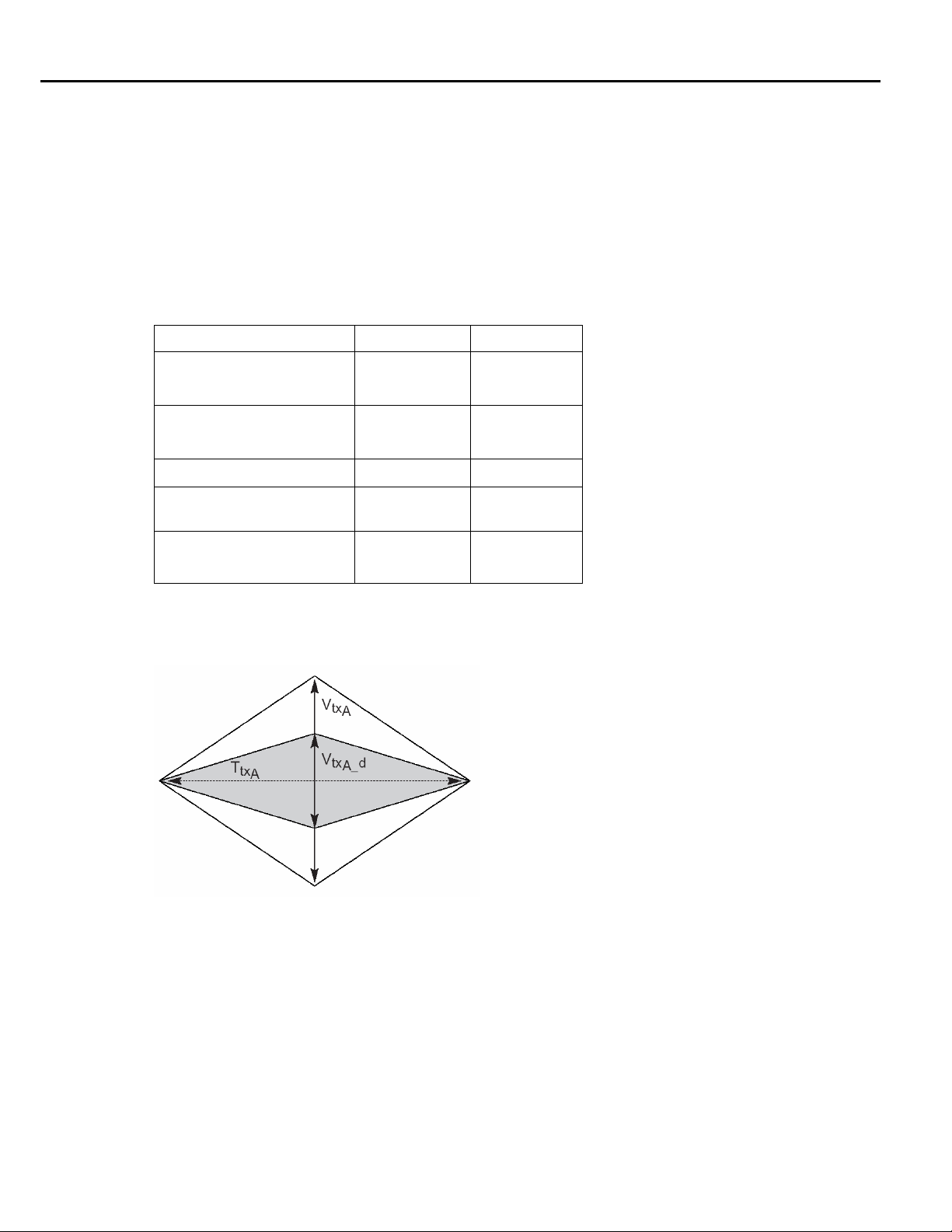
2.5 Add-In Card Transmitter Path Compliance Specifications
Table 5 is derived from the Electrical Mechanical Specifications (CEM). See the CEM Specification for
additional notes and test definitions.
Table 4 – Supported CEM add-in card measurements
Parameter Symbol Gen1
Gen1
Gen2
Rev1.0a
Unit interval UI 400 ps
+/- 300 ppm
V
V
TXA
TXA_d
.514 V (min)
1.2 V (max)
.360 V (min) .360 V (min) TBD
Eye height of transition
bits
Eye height of non-
Rev1.1
400 ps
+/- 300 ppm
.514 V (min)
1.2 V (max)
Rev0.3
200 ps
+/- 300 ppm
TBD
transition bits
T
Eye width across any
250 UIs
Eye width with sample
size of 10
6
UI
Jitter eye opening at
-12
BER 10
Maximum median-max
TXA
In Rev1.0a
T
TXA
In Rev1.1
J
TXA-MEDIAN-to-MAX-JITTER
237 ps (min) Not
Specified
Not Specfied 287 ps (min) TBD
Not Specfied 274 ps (min)
Not Specfied 56.5 ps (max) TBD
TBD
TBD
jitter outlier with sample
size of 10
Maximum median-max
jitter outlier with sample
size of 10
6
6
UI
UI
Not Specfied 63 ps (max)
TBD
6 PCI Express
Page 13
Methods of Implementation
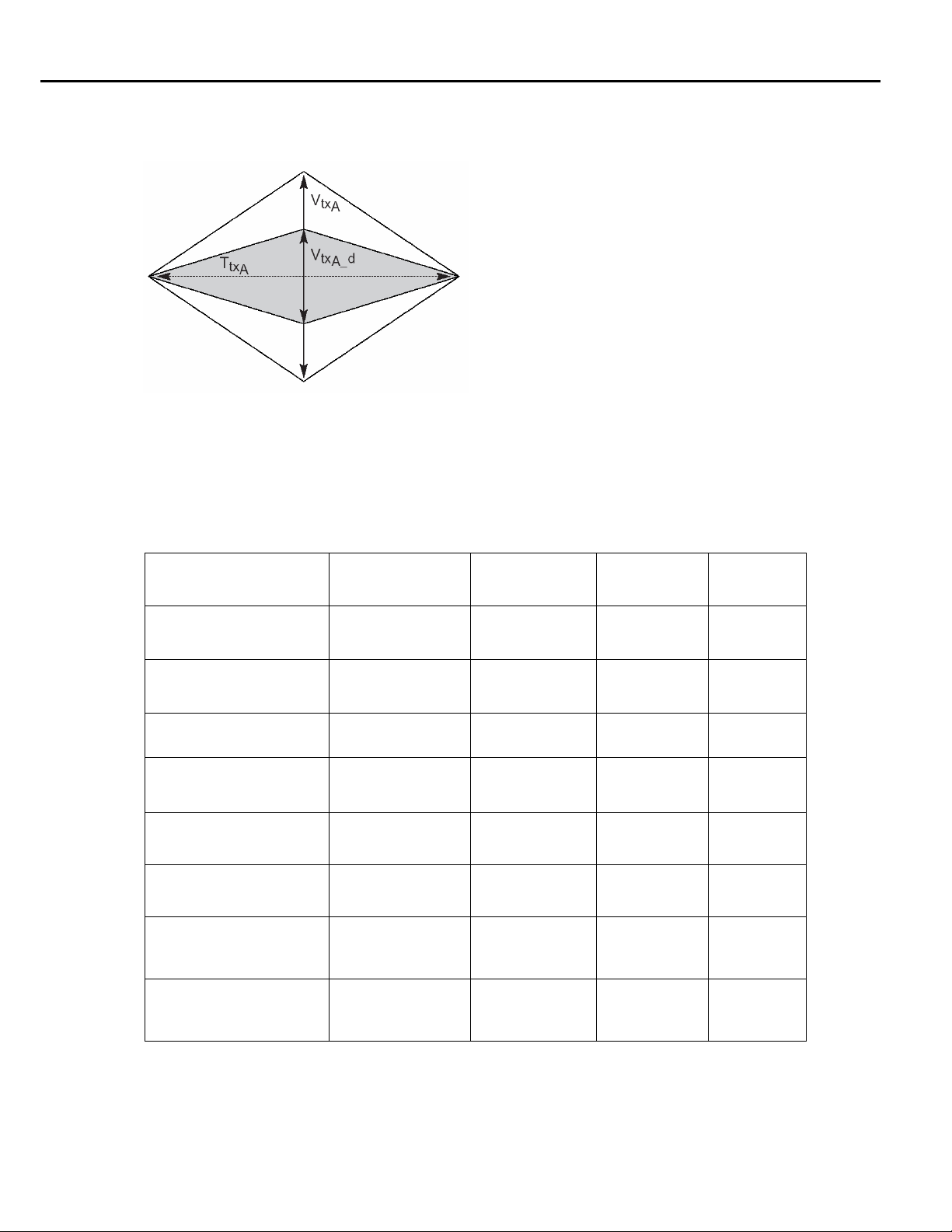
2.6 Add-In Card Compliance Eye Diagrams
The amplitude and jitter masks are derived from the amplitude and jitter specifications in Table 4.
Figure 3: Add-in card compliance eye masks
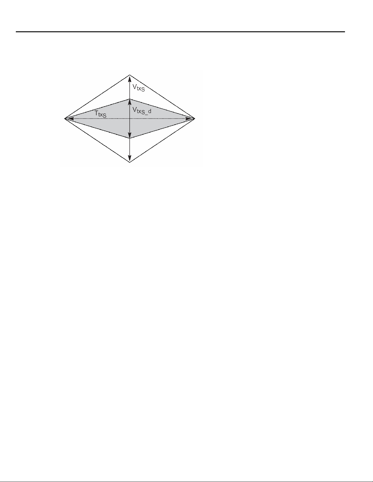
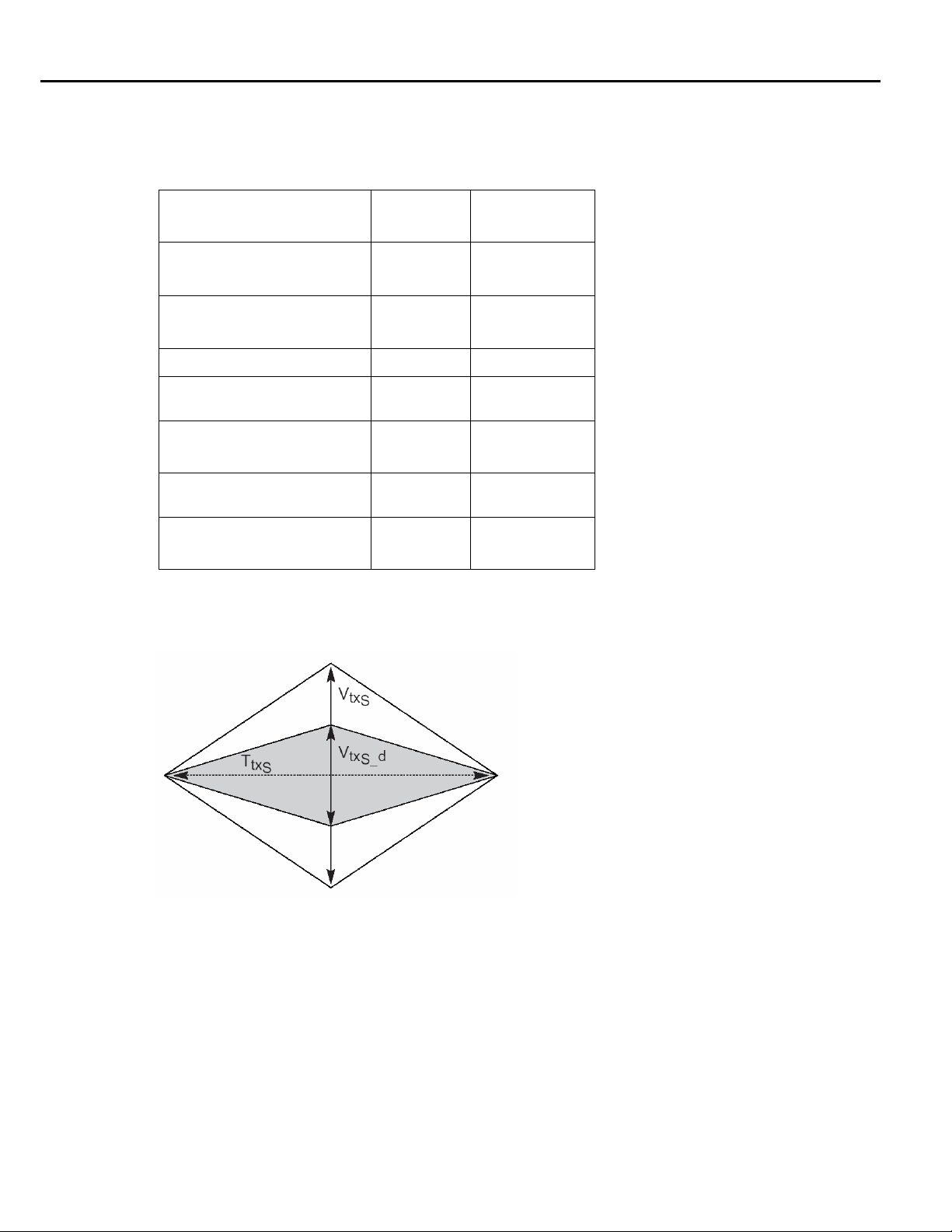
2.7 System Board Transmitter Path Compliance Eye Diagrams
Table 6 is derived from the Electrical Mechanical Specifications (CEM). See the CEM Specification for
additional notes and test definitions.
Table 5 – Supported CEM System Board Measurements
Parameter Symbol Gen1
Gen1
Gen2
Rev1.0a
Unit interval UI 400 ps
+/- 300 ppm
V
Eye height of transition bits
TXS
.274 V (min)
1.2 V (max)
V
Eye height of non-transition
TXS_d
.253 V (min) .253 V (min) TBD
Rev1.1
400 ps
+/- 300 ppm
.274 V (min)
1.2 V (max)
Rev0.3
200 ps
+/- 300 ppm
TBD
bits
T
Eye width across any 250
UIs
Eye width with sample size of
6
10
UI
Jitter eye opening at BER 10
12
Maximum median-max jitter
outlier with sample size of
6
10
UI
Maximum median-max jitter
outlier with sample size of
6
10
UI
-
TXS
18 ps (min) Not Specfied TBD
In Rev1.0a
T
TXS
Not Specfied 246 ps (min) TBD
In Rev1.1
Not Specfied 233 ps (min)
J
TXA-MEDIAN-to-MAX-
JITTER
Not Specfied 77 ps (max) TBD
Not Specfied 83.5 ps (max)
TBD
TBD
PCI Express 7
Page 14
Methods of Implementation
2.8 System Board Compliance Eye Diagrams
The amplitude and jitter masks are derived from the amplitude and jitter specifications in Table 5.
Figure 4: System Board Compliance Eye Masks
8 PCI Express
Page 15
Methods of Implementation
2.9 PCI ExpressModule™ Compliance Specifications
The specifications in this section are taken from the PCI Express ExpressModule™ specification, which is
a companion specification to the PCI Express Base specification. Its primary focus is the implementation
of a modular I/O form factor that is focused on the needs of workstations and servers. Measurements in the
PCE module support add-in card and system transmitter path measurements at the PCI Express connector.
2.9.1 ExpressModule Add-In Card Transmitter Path Specifications
Table 6 is derived from Section 5.4.1 of the ExpressModule Electro-Mechanical Specifications Rev. 1.0.
Table 6 – Supported ExpressModule Add-In Card Measurements
Parameter Symbol Rev1.0
Unit interval UI 400 ps
+/- 300 ppm
V
Eye height of transition Bits
Eye height of non-transition Bits
Eye width with sample size of 106 UI
Jitter eye opening at BER 10
-12
Maximum median-max jitter outlier
with sample size of 10
6
UI
Maximum median-max jitter outlier
with sample size of 10
6
UI
TXA
V
TXA_d
T
TXA
In Rev1.1
J
TXA-MEDIAN-to-
MAX-JITTER
.514 V (min)
1.2 V (max)
.360 V (min)
287 ps (min)
274 ps (min)
56.5 ps (max)
63 ps (max)
Figure 5: ExpressModule add-in card compliance eye masks
PCI Express 9
Page 16
Methods of Implementation
2.9.2 ExpressModule System Board Transmitter Path Compliance Eye Diagrams
Table 7 is derived from Section 5.4.3 of the ExpressModule Electro-Mechanical Specifications Rev. 1.0.
Table 7 – Supported ExpressModule system board measurements
Parameter Symbol Gen1
Unit interval UI 400 ps
Eye height of transition bits
Eye height of non-transition bits
Eye width with sample size of 106
UI
Jitter eye opening at BER 10
Maximum median-max jitter outlier
with sample size of 10
Maximum median-max jitter outlier
with sample size of 10
6
6
V
TXS
V
TXS_d
T
246 ps (min)
TXS
-12
233 ps (min)
J
TXA-MEDIAN-
UI
to-MAX-JITTER
UI
Rev1.0
+/- 300 ppm
.274 V (min)
1.2 V (max)
.253 V (min)
77 ps (max)
83.5 ps (max)
2.9.3 Express Module System Board Compliance Eye Diagrams
The amplitude and jitter masks are derived from the amplitude and jitter specifications in Table 7.
Figure 6: ExpressModule system board compliance eye masks
10 PCI Express
Page 17
Methods of Implementation
2.10 PCI Express External Cabling Specifications
The specifications in this section are taken from the PCI Express External Cabling Specification. Its
primary focus is the implementation of a cabled interconnect. Measurements in the PCE module support
transmitter path and receiver path measurements. These measurements represent the test points at the
transmitter end of the cable and the receiver end of the cable respectively.
2.10.1 External Cabling Transmitter Path Specifications
Table 8 is derived from Section 3.3.1 of the External Cabling Specification Rev. 0.4C.
Table 8 – Supported external cabling transmitter path measurements
Parameter Symbol Rev0.4C
Unit interval UI 400 ps
+/- 300 ppm
V
V
T
TXA
TXA_d
TXA
.659 V (min)
1.2 V (max)
.456 V (min)
309 ps (min)
296 ps (min)
Eye height of transition bits
Eye height of non-transition bits
Eye width with sample size of
6
10
UI
Jitter eye opening at BER 10
-12
2.10.2 Cable (Transmitter Side) Eye Diagrams
The amplitude and jitter masks are derived from the amplitude and jitter specifications in Table 8.
Figure 7: Cable (transmitter side) compliance eye masks
PCI Express 11
Page 18
Methods of Implementation
2.10.3 External Cabling Receiver Path Specifications
Table 9 is derived from Section 3.3.2 of the External Cabling Specification Rev. 0.4C.
Table 9 – Supported CEM System Board Measurements
Parameter Symbol Gen1
Unit interval UI 400 ps
Eye height of transition bits
Eye height of non-transition bits
Eye width with sample size of 106
UI
Jitter eye opening at BER 10
2.10.4 Cable (Receive Side) Eye Diagrams
Rev1.0
+/- 300 ppm
V
RXA
.219 V (min)
1.2 V (max)
V
RXA_d
T
247 ps (min)
RXA
-12
234 ps (min)
.200 V (min)
The amplitude and jitter masks are derived from the amplitude and jitter specifications in Table 9.
Figure 8: Cable (receiver side) compliance eye masks
12 PCI Express
Page 19
Methods of Implementation
2.11 Reference Clock Compliance Specifications
Table 10 is derived from section 2.1 of the Gen1 Rev1.1 Electrical Mechanical Specifications (CEM) and
Gen2 Base specifications.
Table 10 – Supported reference clock measurements
Parameter Symbol Gen1
Rev1.1
Rise edge rate
Rise Edge Rate
0.6 V/ns (min)
4.0 V/ns (max)
Fall edge rate
Fall Edge Rate 0.6 V/ns (min)
4.0 V/ns (max)
Differential input high voltage
V
IH
150 mV (max) 150 mV (max)
Differential input low voltage VIL -150 mV (min) -150 mV (min)
Absolute period (including jitter
and spread spectrum)
T
PERIOD_ABS
9.847 ns (min)
10.203 ns (max)
Duty cycle Duty Cycle 40% (min)
60% (max)
Maximum peak-peak filtered
Jitter @ 10
-12
BER 108 ps (max) Not
phase jitter
Gen2
Rev0.3
0.6 V/ns (min)
4.0 V/ns (max)
0.6 V/ns (min)
4.0 V/ns (max)
9.997 ns (min)
10.053 ns (max)
40% (min)
60% (max)
Specified
Maximum peak-peak filtered
phase jitter
RMS jitter T
Jitter @ 10-6 BER 86 ps (max) Not
Specified
3.1 ps (max)
CLK_RJ
PCI Express 13
Page 20
Methods of Implementation
3 Preparing to Take Measurements
3.1 Required Equipment
The following equipment is required to take the measurements:
• Oscilloscope Selection:
ο Gen1 (2.5 Gb/s) – The PCI-SIG recommends a minimum of 6 GHz system BW for Gen1
Measurements. Tektronix models that meet this recommendation are: All the TDS6000B/C Series
instruments and the TDS7704B.
ο Gen2 (5 Gb/s) – It is recommended that >12 GHz system BW is used for Gen2. This ensures the
th
5
harmonic is represented in the measurements. Tektronix models that meet this
recommendation are TDS6000C models.
• RT-Eye software (Opt. RTE) and PCI Express Compliance Module (PCE) installed.
• Probes – probing configuration is MOI specific. Refer to each MOI for proper probe configuration.
• Test fixture breakout from transmitter to differential SMA connectors. A Compliance Base Board
(CBB) used for add-in card compliance tests and a Compliance Load Board (CLB) used for system
compliance tests are available through the PCI-SIG at the following URL:
http://www.pcisig.com/specifications/ordering_information/ordering_information
• Test fixtures for notebook testing are available from the following URL:
http://www.expresscard.org/web/site/testtools.jsp
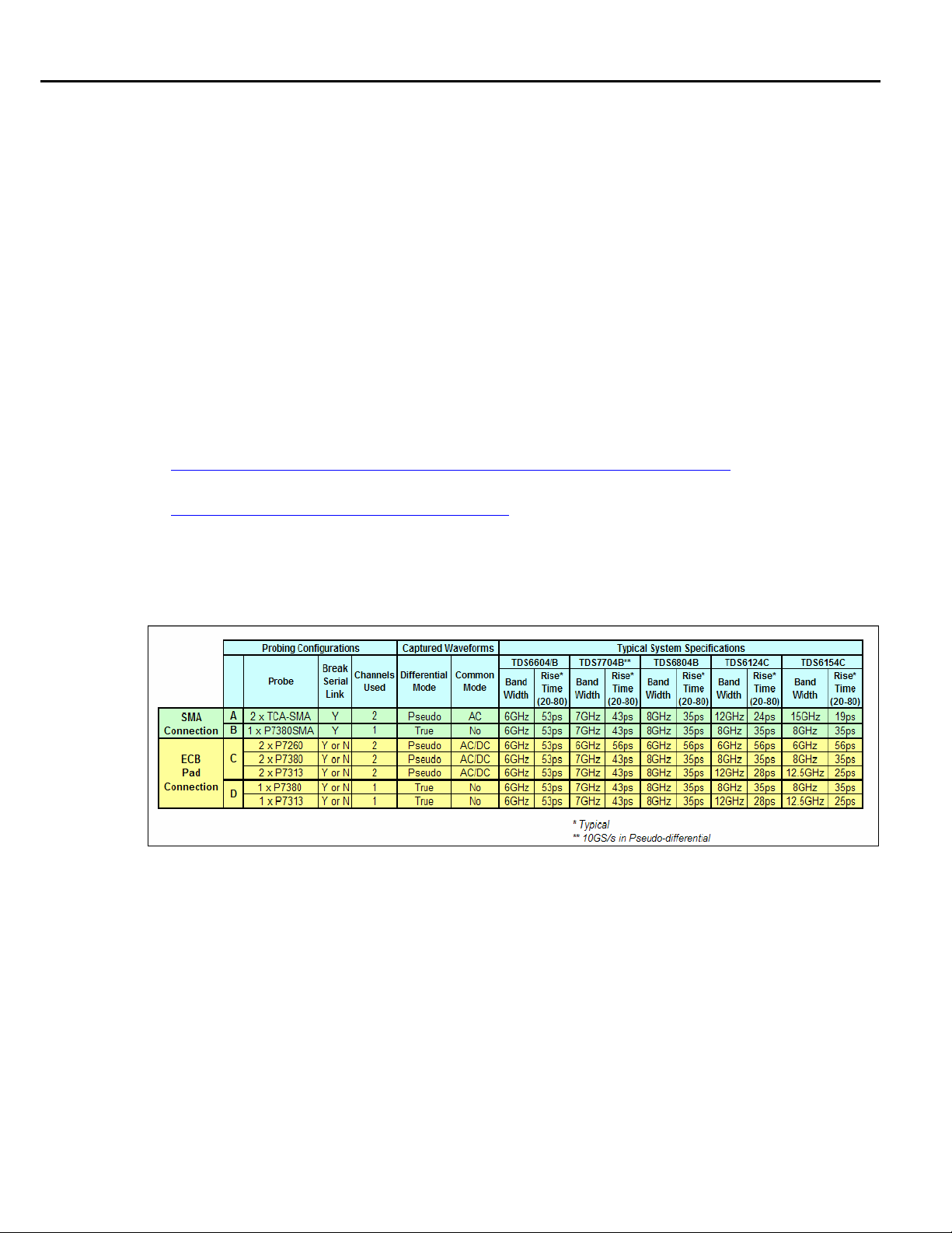
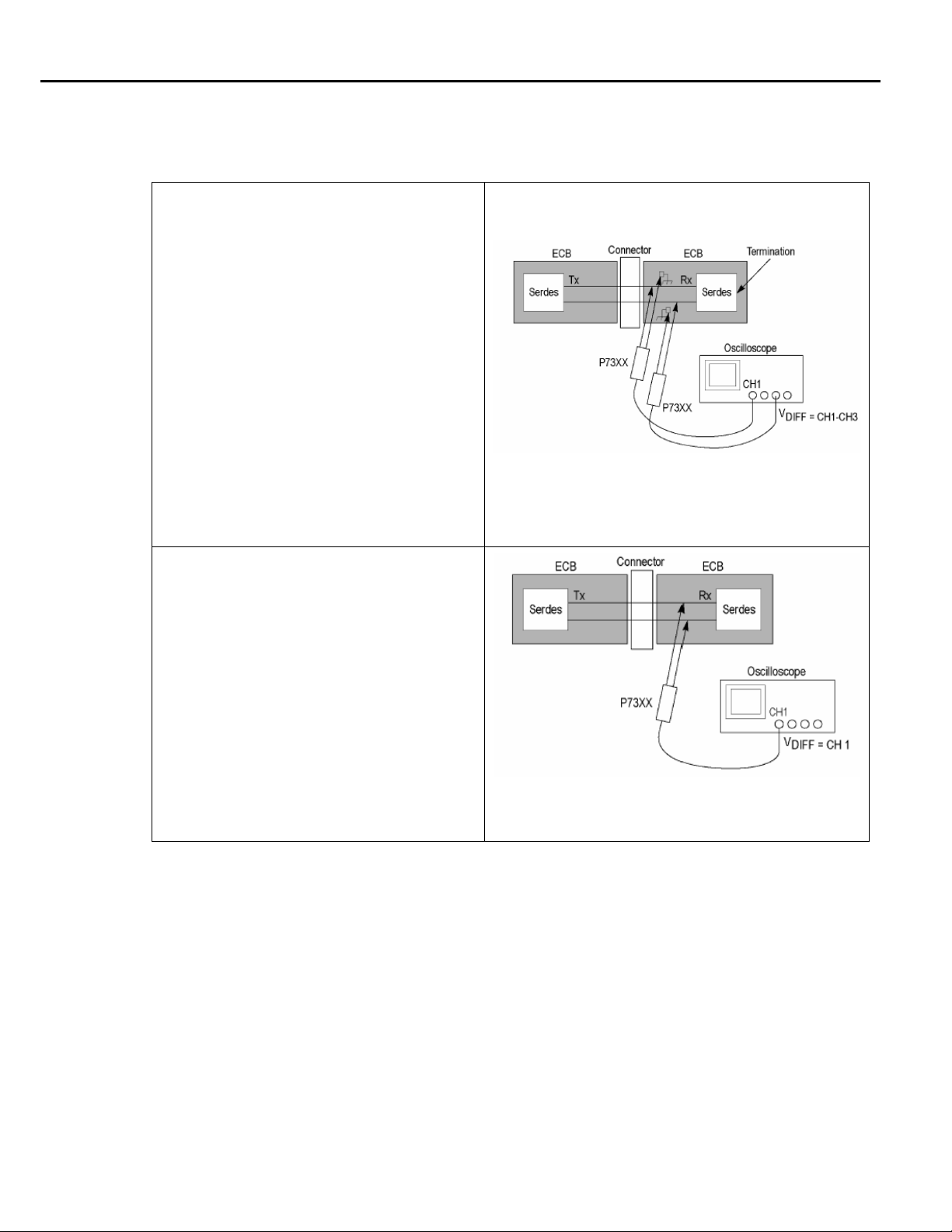
3.2 Probing Options for Transmitter Testing
The first step is to probe the link. Use one of the following four methods to connect probes to the link.
Table 11 – Probing configurations for a PCI express link
14 PCI Express
Page 21
Methods of Implementation
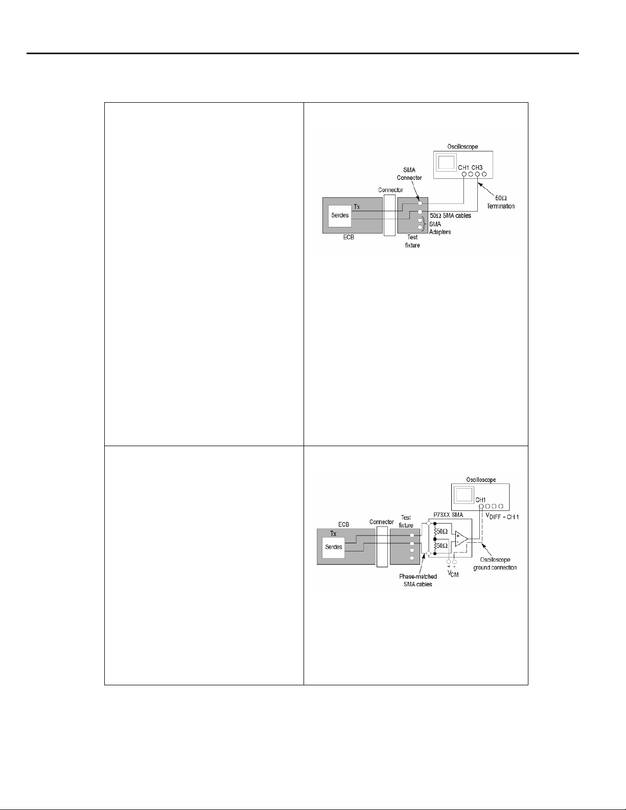
3.2.1 SMA Input Connection
1. Two TCA-SMA inputs using SMA
cables (Ch1) and (Ch3)
The differential signal is created by
the RT-Eye software from the math
waveform Ch1-Ch3. The Common
mode AC measurement is also
available in this configuration from
the common mode waveform
(Ch1+Ch3)/2. This probing technique
requires breaking the link and
terminating into a 50 Ω/side
termination of the oscilloscope.
While in this mode, the PCI Express
SerDes will transmit the compliance
test pattern. Ch-Ch de-skew is
required using this technique because
two channels are used. This
configuration does not compensate
for cable loss in the SMA cables. The
measurement reference plane is at the
input of the TCA-SMA connectors
on the oscilloscope. Any cable loss
should be measured and entered into
the vertical attenuation menu for
accurate measurements at the SMA
cable attachment point.
Probe Configuration A
SMA Psuedo-differential
2. One P7380SMA differential active
probe (Ch1)
The differential signal is measured
across the termination resistors inside
the P7380SMA probe. This probing
technique requires breaking the link.
While in this mode, the PCI Express
SerDes will transmit the compliance
test pattern. Matched cables are
provided with the P7380 probe to
avoid introducing de-skew into the
system. Only one channel of the
oscilloscope is used. The P7380SMA
provides a calibrated system at the
Probe Configuration B
SMA Input Differential Probe
Test Fixture attachment point,
eliminating the need to compensate
for cable loss associated with the
probe configuration A.
PCI Express 15
Page 22
Methods of Implementation
3.2.2 ECB pad connection
3. Two P7300 or P7260 active probes
(Ch1) and (Ch3)
The differential signal is created by the
RT-Eye software from the math
waveform Ch1-Ch3. The Common mode
AC measurement is also available in this
configuration from the common mode
waveform (Ch1+Ch3)/2. This probing
technique can be used for either a live
link that is transmitting data, or a link that
has terminated into a “dummy load.” In
both cases, the single-ended signals
should be probed as close as possible to
the termination resistors on both sides
with the shortest ground connection
possible. Ch-Ch de-skew is required
using this technique because two
channels are used.
Probe Configuration C
Two Single-Ended Active Probes
4. One P7380 Differential probe (Ch1)
The differential signal is measured
directly across the termination resistors.
This probing technique can be used for
either a live link that is transmitting data,
or a link that is terminated into a “dummy
load.” In both cases, the signals should be
probed as close as possible to the
termination resistors. De-skew is not
necessary because a single channel of the
oscilloscope is used.
Probe Configuration D
One Differential Active Probe
16 PCI Express
Page 23

Methods of Implementation
3.3 Initial Oscilloscope Setup
After connecting the DUT by following the proper probing configuration for the test, click DEFAULT
SETUP and then Autoset to display the serial data bit stream.
3.4 Running the RT-Eye Software
1. On non-B or non-C model oscilloscopes (Example: TDS6604), Go to File > Run Application > RT-
Eye Serial Compliance and Analysis. For B and C models (Example: TDS7704B, TDS6154C), go to
App > RT-Eye Serial Compliance and Analysis.
Figure 9: Default menu of the RT-Eye software
Figure 9 shows the oscilloscope display. The default mode of the software is the Serial Analysis module
(Opt.RTE). This software is intended for generalized Serial Data analysis on 8B/10B encoded copper
links.
2. Select the PCI Express Compliance Module from the Modules pull-down list.
Figure 10: Choosing PCI Express Compliance Module.
PCI Express 17
Page 24

Methods of Implementation
Note: If PCI Express does not appear in the list (as in Figure 10), the PCI Express Compliance Module
(Opt. PCE) has not been installed.
The rest of this MOI document details the use of the PCI Express Compliance Module to perform
electrical compliance measurements.
For additional information, refer to the online help for the RT-Eye software available through the Serial
Analysis Module help menu.
3.5 Configuring the Software to take measurements
Before you take compliance measurements, configure the software as follows:
3.5.1 Select Standard
Using the Specification pull-down menu, select the desired specification to be measured.
The selections are:
Rev1.0a – 2.5 Gb/s
Rev1.1 – 2.5 Gb/s
Gen2 – 5 Gb/s
Use SIG-TEST – refer to Section 8
3.5.2 Select Test Point
Use the Test Point pull-down list to select the desired test point.
Selections in the Test Point menu are dependent on which specification is selected. The selections are as
follows:
If Rev1.0a – 2.5 Gb/s is selected as Standard:
Receiver
Driver
CEM: Add-In
CEM: System
Mobile LP: Transmitter
User Defined – Using Dynamic Test Points – See Section 9 for definition
If Rev1.1 – 2.5 Gb/s is selected as Standard:
18 PCI Express
Page 25

Methods of Implementation
Base: Transmitter
Base: Receiver
CEM: Add-In
CEM: System
Cable: Transmitter
Cable: Receiver
ExpressModule: System TX
ExpressModule: TX Path
User Defined – Using Dynamic Test Points – See Section 9 for definition
Reference Clock
If Gen2 – 5Gb/s is selected as Standard:
Base: Transmitter
Base: Receiver
User Defined – Using Dynamic Test Points – See Section 9 for definition
Reference Clock
3.5.3 Select Probe Type
Using the Probe Type pull-down menu, select the desired probing configuration.
The selections are:
Single-Ended – Select if Pseudo-differential (probing configurations A or C from Section 3.2) is being
used.
Differential – Select use if true differential (probing configurations B or D from Section 3.2) is being
used.
3.5.4 Select Measurements
In the Measurement > Select menu, select the desired measurements. Measurements can be selected
either manually or as a group by using Select Required. If a measurement has a pass/fail limit associated
with it in the test point file, it will be selected when Select Required is clicked. Measurements with
pass/fail limits will show up in the Results Summary panel when the compliance test is run.
Measurement results of selected measurements, which do not have limits associated with them can be
viewed in the Results Details panel.
PCI Express 19
Page 26

Methods of Implementation
Figure 11: Measurement Select menu
3.5.5 Configure Source of Waveforms
Use the Measurements > Configure > Source menu to select the source of the measured data.
Figure 12: Configure Source menu
Source selections are dependent on which probe type is selected. The selections are as follows:
If Differential is selected as Probe Type:
Live/Ref source selection (uses single differential signal as data source)
o Live channel selections–Ch1, Ch2, Ch3, Ch4
o Reference waveform selections–Ref1, Ref2, Ref3, Ref4
File source selection
o File selection – Uses one saved .csv as file as differential data source
If Single-Ended is selected as Probe Type:
Live/Ref source selection (uses two single-ended signals as data source)
o Live channel selections–(Ch1-Ch3), (Ch1-Ch4), (Ch2-Ch3), (Ch2-Ch4)
o Reference waveform selections –Refx-Refy, where x and y are integers 1-4
File source selection
o File selection–Uses two saved .csv files as single-ended data source
20 PCI Express
Page 27

Methods of Implementation
3.5.6 Configure Clock Recovery
Use the Measurements> Configure> Meas Config menu to select the type of clock recovery to be used.
Figure 13: Measurement Configuration menu
Selections in the General Config panel depend on the specification that has been chosen. The selections
are defined as follows:
If Rev1.0a – 2.5 Gb/s is selected as Standard:
SSC (Scan Off) – 3500:250 clock recovery with no waveform scanning is used.
SSC (Scan On) – 3500:250 clock recovery with waveform scanning is used.
If Rev1.1 – 2.5 Gb/s is selected as Standard:
SSC (Scan Off) – 3500:250 clock recovery with no waveform scanning is used.
SSC (Scan On) – 3500:250 clock recovery with waveform scanning is used.
Clean Clock – A 1st Order PLL with a corner frequency of 1.5 MHz is used to recover the clock.
If Gen2 – 5 Gb/s is selected as Standard:
SSC (Scan Off) – 3500:250 clock recovery with no waveform scanning is used.
SSC (Scan On) – 3500:250 clock recovery with waveform scanning is used.
Clean Clock – A 1st Order PLL with a corner frequency of 3 MHz is used to recover the clock.
PCI Express 21
Page 28

Methods of Implementation
When to use SSC selection:
SSC is the only selection in Rev1.0a and is optional in the Rev1.1 and Gen2. It is to be used when a clean
clock source is not available or if SSC is turned on in a system. The following describes how the clock is
recovered using this technique:
The “SmartGating” feature of the RT-Eye application is used to set up a software clock recovery window
and an analysis window. This feature is available (and configurable) outside the PCI Express
Compliance Module in the Measurements> Configure> SmartGating menu of the Serial Analysis
module.
The clock recovery window is 3500 consecutive UIs and the Mean of the UIs is used as the reference
clock. The first 3500 UIs in the acquisition are used.
An analysis window is established to be 250 UIs centered in the 3500 UI clock recovery window. The
placement of mask is based on the median of the 250 UI analysis windows.
• Optionally, the “Scan On” check box can be selected. When checked, the clock recovery and analysis
waveform will scan the waveform by stepping the 3500:250 window across the waveform in 100 UI
steps. This technique is same as the PCI-SIG SigTest software, used to determine compliance over a
single shot waveform.
When to use the Clean Clock selection:
The clean clock selection is not available in Rev1.0a and is optional in the Rev1.1 and Gen2. It is to be
used when a clean reference clock is available. As defined in the base specification, the clock
recovery function to be used is a 1st order PLL with a corner frequency of 1.5 MHz (Rev1.1) and
1 MHz (Gen2). In the Gen2 specification, a mask function is provided. The PCI Express module
implements a first order PLL with a 1 MHz cutoff frequency. The first order PLL can be changed to a
second order PLL by using a dynamic test point file as described in section 9.
Figure 14: Clock recovery mask function in Gen2 base specification
22 PCI Express
Page 29

Methods of Implementation
3.5.7 Configure Plots
The plots in the PCI Express Module are configured automatically. If the Jitter@BER measurement is
not selected, eye diagrams with masks will be displayed in the Plot Summary window (Figure 15a). The
eye diagram can either be a double plot showing transition bit and non-transition bit or can be a single
plot showing all bits depending on the test point selected.
Figure 15a: Plot Summary when Jitter@BER measurement is not selected
If the Jitter@BER measurement is selected, then a Jitter Spectrum and Bathtub Curve are added to the
Plot Summary window.
Figure 15b: Plot Summary when the Jitter@BER measurement is selected
PCI Express 23
Page 30

Methods of Implementation
4 PCI Express Transmitter Compliance Testing
This section provides the Methods of Implementation (MOIs) for Transmitter tests using a Tektronix realtime oscilloscope, probes, and the RT-Eye compliance software.
4.1 Probing the link for TX compliance
Use probing configuration B from Section 3.2. Connect the positive leg of the differential signal to the ‘+’
SMA connector and the negative leg of the differential signal to the ‘– ‘SMA connector on the P7380SMA
differential probing system.
Alternatively, use probe configuration A, to connect Ch1 and Ch3 to the inputs of an oscilloscope that has
20 GS/s sample rate available on two channels (TDS6604 or TDS6000B Series).
Since the link is broken and terminated into a 50 Ω load, the compliance pattern is defined in the base
specification will be transmitted automatically.
4.2 TX Compliance Test Load
The compliance test load for driver compliance is shown in the base specification.
Figure 16: Driver compliance test load
4.3 Running a Transmitter (TX) Compliance Test
The MOI for each of the transmitter measurements is documented in the following sections. All transmitter
compliance measurements can be selected and run simultaneously with the same acquisition. See Section
3.5 for more info on configuring the module to make measurements.
To perform a compliance test of all transmitter measurements:
1. Select the desired Specification from the Specification pull-down list.
2. Select the desired Test Point from the Test Point pull-down list.
3. In the Measurement Select menu (Figure 17), choose Single-Ended (for probe configuration A defined
in Section 3) or Differential (for probe configurations B defined in Section 3) as the probe type.
4. Click Configure to configure the source and clock recovery method to be used.
5. Click Source tab to configure the data source.
24 PCI Express
Page 31

Methods of Implementation
6. Click General Config tab to select the desired clock recovery method.
7. Return the Measurement Select menu by clicking Select.
Figure 17: Measurements Select menu setup
8. Click Select Required and/or select desired measurements manually.
9. Click Autoset in the RT-Eye Measurement Select menu. This will automatically set up the
oscilloscope vertical, horizontal, and measurement reference levels for the compliance test.
10. Click Start.
Figure 18 shows the result of a Transmitter Compliance test on a signal that passes the driver tests at all
three TX compliance test points.
Figure 18: Result of a successful transmitter compliance test
PCI Express 25
Page 32

Methods of Implementation
4.3.1 TX Unit Interval Measurement MOI
Test Definition Notes from the Specification:
- UI (Unit Interval) is specified to be +/- 300 ppm
- UI does not account for SSC dictated variations
Definition: UI is defined in the base specification.
Limits:
Refer to Table 2 for specified limits on UI measurement.
Test Procedure:
Ensure that UI is selected in the Measurements> Select menu.
Measurement Algorithm:
This measurement is made over the Analysis Window of 250 consecutive bits defined in Section 3.4
(Base specification).
The Unit Interval measurement calculates the cycle duration of the recovered clock.
)()1()( ntntnUI
CLKRCLKR −−
AVG
−+=
=
))(( nUIMeanUI
Where:
CLKRt−
is a recovered clock edge
n is the index to UI in the waveform
26 PCI Express
Page 33

Methods of Implementation
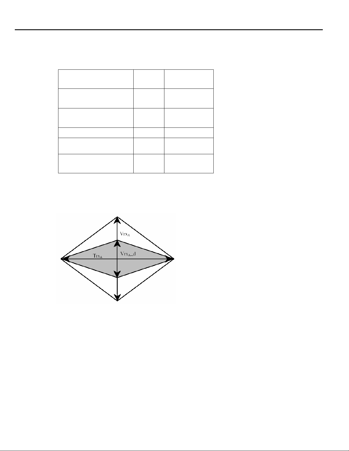
4.3.2 TX Differential Pk-Pk Output Voltage MOI
Definition:
V
pDIFFpTX
−−
(Differential Output Pk-Pk Voltage) is defined in the base specification. This measurement is
solved by two measurements. One is Differential Peak Voltage measurement and the other is Eye Height:
Transition Bits measurement. If you select Differential Voltage and Eye Width/Eye Height, you will get
five measurements: Eye Height, Eye Height: Transition Bits, Eye Height: Non-Trans Bits, Eye Width
and Differential Peak Voltage.
Test Definition Notes from the Specification:
-
−∗=
VVV
||2
−−+−−−
DTXDTXpDIFFpTX
- Specified at the measurement point into a timing and voltage compliance test load as shown in the base
specification and measured over specified number of UIs. Also refer to the transmitter compliance eye
diagram shown in the base specification.
Limits:
Refer to Table 2 for specified limits on the
V
pDIFFpTX
−−
measurement.
Test Procedure:
Ensure that Differential Voltage and Eye Width/Eye Height are selected in the Measurements> Select
menu.
Measurement Algorithm:
Differential Peak Voltage Measurement: The Differential Peak Voltage measurement returns two
times the larger of the Min or Max statistic of the differential voltage waveform.
)))(());(((2 ivMinivMaxMaxV
DIFFDIFFPKDIFF∗=−
Where:
i is the index of all waveform values
v
DIFF
is the differential voltage signal
PCI Express 27
Page 34

Methods of Implementation
−
−
=
Eye Height Measurement: The measured minimum vertical eye opening at the UI center as shown in
the plot of the eye diagram. There are three types of eye height values:
Eye Height:
Where:
MINHIEYEV−−
MAXLOEYEV−−
Eye Height – Transition:
VVV
−=
MAXLOEYEMINHIEYEHEIGHTEYE
−−−−−
is the minimum of the high voltage at mid UI
is the maximum of the low voltage at mid UI
=
Where:
V
V
Eye Height – Non-Transition:
Where:
V
V
MINTRANHIEYE
−−−
is the minimum of the high transition bit eye voltage at mid UI
MAXTRANLOEYE
−−−
is the maximum of the low transition bit eye voltage at mid UI
MINNTRANHIEYE
−−−
is the minimum of the high non-transition bit eye voltage at mid UI
MAXNTRANLOEYE
−−−
is the maximum of the low non-transition bit eye voltage at mid UI
VVV
VVV
MAXTRANLOEYEMINTRANHIEYETRANHEIGHTEYE
−−−−−−−−
MAXNTRANLOEYEMINNTRANHIEYENTRANHEIGHTEYE
−−−−−−−−
28 PCI Express
Page 35

Methods of Implementation
4.3.3 TX De-Emphasized Differential Output Voltage (Ratio) MOI
Definition:
(De-Emphasized Differential Output Voltage (Ratio)) is defined in the base specification.
RATIODETXV−−
Test Definition Notes from the Specification:
- This is the ratio of the
V
of the first bit after a transition.
pDIFFpTX
−−
V
of the second and following bits after a transition divided by the
pDIFFpTX
−−
- Specified at the measurement point into a timing and voltage compliance test load as shown in the base
specification over the specified number of UIs. Also refer to the transmitter compliance eye diagram
shown the base specification.
Limits:
Refer to Table 2 for specified limits on the
measurement.
RATIODETXV−−
Test Procedure:
Ensure that De-Emphasis is selected in the Measurements > Select menu.
Measurement Algorithm:
nd
The de-emphasis measurement calculates the ratio of any non-transition eye voltage (2
voltage succeeding an edge) to its nearest preceding transition eye voltage (1
st
eye voltage succeeding an
, 3rd, etc. eye
edge). In Figure 19, it is the ratio of the black voltages over the blue voltages. The results are given in dB.
Figure 19: De-emphasis measurement
PCI Express 29
Page 36

Methods of Implementation
−
=
)(
dBmDEEM
=
−−
NTRANHIEYE
−−
TRANHIEYE
)(
mv
)(
nv
or
)(
dBmDEEM
=
−−
NTRANLOEYE
−−
TRANLOEYE
)(
mv
)(
nv
Where:
TRANHIEYEv−−
is the high voltage at mid UI following a positive transition
TRANLOEYEv−−
is the low voltage at mid UI following a negative transition
NTRANHIEYEv−−
is the high voltage at mid UI following a positive transition bit
NTRANLOEYEv−−
is the low voltage at mid UI following a negative transition bit
m is the index for all non-transition UIs
n is the index for the nearest transition UI preceding the UI specified by m
4.3.4 Minimum TX Eye Width MOI
Definition:
(Minimum TX Eye Width) is defined in the base specification. Note that the definition of the
EYETXT−
Eye width changes from Rev1.x to the Gen2. See Section 4.3.9 for the Gen2 definition. For Gen1, the
Eye width is a histogram-based measurement that is defined as follows.
Test Definition Notes from the Specification:
- The maximum Transmitter jitter can be derived as
- Specified at the measurement point into a timing and voltage compliance test load as shown in the base
specification and measured over the specified number of UIs. Also refer to the transmitter compliance
eye diagram shown in the base specification.
Note: The median is not the same as the mean. The jitter median describes the point in time where the
number of jitter points on either side is approximately equal as opposed to the averaged time value.
Limits:
Refer to Table 2 for specified limits on the
measurement.
EYETXT−
TT
1
EYETXJITTERTXMAX
−−
Test Procedure:
Ensure that De-Emphasis is selected in the Measurements> Select menu.
30 PCI Express
Page 37

Methods of Implementation
Measurement Algorithm:
The measured minimum horizontal eye opening at the zero reference level as shown in the eye diagram.
TIEUIT
−=
PkPkAVGWIDTHEYE
−−
Where:
UI is the average UI
AVG
TIE
is the Peak-Peak TIE
PkPk
−
4.3.5 TX Median-to-Max Jitter MOI
Definition:
T
MAXJITTERtoEYEMEDIANTX
−−−
median.) is defined in Rev1.0a of the base specification.
Limits:
Refer to Table 2 for
Test Procedure:
Ensure that TIE is selected in the Measurements> Select menu.
Measurement Algorithm:
The measured time difference between a data edge and a recovered clock edge.
Where:
(maximum time between the jitter median and maximum deviation from the
T
)()()( ntntntie
DATDATR−=−
MAXJITTERtoEYEMEDIANTX
−−−
measurement.
t
DAT
is the original data edge
DATRt−
is the recovered data edge (for example, the recovered clock edge corresponding to the UI
t
boundary of
DAT
)
n is the index of all edges in the waveform
PCI Express 31
Page 38

Methods of Implementation
4.3.6 TX Output Rise/Fall Time MOI
Definition:
,
RISETXT−
(D+/D- TX Output Rise/Fall Time) is defined in the base specification.
FALLTXT−
Test Definition Notes from the Specification:
- Specified at the measurement point into a timing and voltage compliance test load as shown in the base
specification and measured over the specified number of TX UIs.
- Measured between 20-80% at transmitter package pins into a test load for both
V and
+−DTX
V
−−DTX
Limits:
Refer to Table 2 for specified limits on
,
RISETXT−
measurements.
FALLTXT−
Test Procedure:
Ensure that Rise Time and Fall Time are selected in the Measurements> Select menu.
Note: Rise/Fall time D+ and D- measurements show up when the probe type is single-ended. Rise Time
measurements show up when differential probe type is used. Error in Rise/Fall time measurements
includes bandwidth limitations of the system in some cases.
Measurement Algorithm:
Rise/Fall time is limited to only rising or falling edges of consecutive transitions for transmitter
measurements. Rise/Fall Time is taken independently on each single-ended waveform sources when you
use two single-ended probes as the signal source. Differential signal Rise/Fall Time show up when you
select Differential probe type.
Rise Time: The Rise Time measurement is the time difference between when the V
is crossed and the V
reference level is crossed on the rising edge of the waveform.
REF-LO
−=
)()()( jtitnt
LOHIRISE ++
reference level
REF-HI
Where:
t is a Rise Time measurement
RISE
t is a set of HIt for rising edges only
+HI
t is a set of LOt for rising edges only
+LO
i and j are indexes for nearest adjacent pairs of
t and
+LO
t .
+HI
n is a the index of rising edges in the waveform
32 PCI Express
Page 39

Methods of Implementation
−
Rise Time for )(tv
D +++++
RISE
and for
t
D–FALL
(n) = t
D−
)(tv
D–LO–
is as follows:
D+
−=
(i) – t
D–HI–
LODHID
(j)
)()()( jtitnt
Fall Time: The Fall Time measurement is the time difference between when the V
crossed and the V
=
reference level is crossed on the falling edge of the waveform.
REF-LO
)()()( jtitnt
HILOFALL −−
Where:
t
is a Fall Time measurement
FALL
t
is set of tHI for falling edge only
HI–
t
is set of tLO for falling edge only
LO–
i and j are indexes for nearest adjacent pairs of t
LO–
and t
HI–
.
reference level is
REF-HI
n is the index to falling edges in the waveform
Fall Time for v
D
FALL
and for v
D −−
D–
FALL
(t) is as follows:
D+
D
++
(t)
D
−−
LO
−
LO
−=
−
−=
HID
D
+
HI
)()()( jtitnt
−
)()()( jtitnt
PCI Express 33
Page 40

Methods of Implementation
4.3.7 TX AC Common Mode Output Voltage MOI
Definition:
ACpCMTXV−−
nomenclature ACp is retained to be consistent with the specification. However, the measurement is
defined and reported by the PCI Express module as an RMS value, not a Pk value.
Test Definition Notes from the Specification:
(RMS AC Pk Common Mode Output Voltage) is defined in Rev1.0a Base Specification. The
+
VV
DTXDTX
=
ACpCMTX
−−
(|
RMSV
2
−−+−
=−
−−−−
|)|
ofDCVV
avgDCCMTXDCCMTX
)(
+
VV
DTXDTX
−−+−
|
2
- Specified at the measurement point into a timing and voltage compliance test load as shown in the base
specification and measured over the specified number of TX UIs.
Limits:
Refer to Table 2 for specified limits on
measurement.
ACpCMTXV−−
Test Procedure:
Ensure that AC CM Voltage is selected in the Measurements> Select menu.
Note: This measurement is available only when the probe type is single-ended.
Measurement Algorithm:
AC CM RMS Voltage: The AC Common Mode RMS Voltage measurement calculates the RMS
statistic of the common mode voltage waveform with the DC value removed.
=
))(()( ivRMSiv
MACCMRMSAC −−−
Where:
i is the index of all waveform values
is the RMS of the AC common mode voltage signal
CMRMSACv−−
is the AC common mode voltage signal
MACv−
34 PCI Express
Page 41

Methods of Implementation
4.3.8 TX Delta DC Common Mode Voltage MOI
Definition:
V
−−−−
(Absolute Delta of DC Common Mode Voltage between D+ and D-) is defined in
DELTALINEDCCMTX
the base specification.
Test Definition Notes from the Specification:
25||
≤−
−−−−+−−−
DDCCMTXDDCCMTX
=
=
VofDCV
)(
VofDCV
)(
mVVV
||
+−+−−
DTXavgDDCTXCM
||
−−−−−−
DTXavgDDCCMTX
- Specified at the measurement point into a timing and voltage compliance test load as shown in the base
specification and measured over the specified number of UIs.
Limits:
Refer to Table 2 for specified limits on
V
measurement.
DELTALINEDCCMTX
−−−−
Test Procedure:
Ensure that Differential Average is selected in the Measurements> Select menu.
Measurement Algorithm:
The Differential Average measurement returns the mean of the differential voltage waveform.
))(( ivMeanV
DIFFAVGDIFF=−
Where:
i is the index of all waveform values
v
DIFF
is the differential voltage signal
PCI Express 35
Page 42

Methods of Implementation
4.3.9 TX Total Jitter@BER MOI
Definition:
The jitter eye opening
is re-defined Gen2 specification to statistical relevance to 10
EYETXT−
-12
BER. A
detailed definition can be found in section 4.4.8 of the Gen2 base specification.
Test Definition Notes from the Gen2 (Rev0.3) Specification:
- Does not include SSC or Refclk. Jitter Includes Rj at 10
-12
.
- Transmitter jitter is measured by driving the transmitter under test with a low jitter “ideal” clock and
connecting the DUT to a reference load.
- Transmitter jitter must be post-processed with a filtering function that represents the worst case CDR
tracking BW.
Limits:
Refer to Table 2 for specified limits on the
measurement.
EYETXT−
Test Procedure:
Ensure that Jitter@BER is selected in the Measurements> Select menu.
Measurement Algorithm:
Total jitter in the PCI Express Compliance Module uses the Arbitrary Pattern Jitter Algorithm in RT-Eye
to establish
. To understand the complete algorithm, one must understand RT-Eye’s spectrum
EYETXT−
approach to jitter measurements.
4.3.10 Spectrum Analysis Based Rj/Dj Separation on Repeating Pattern
Dj components can be identified in a jitter spectrum under a set of conditions. PJ will appear as spectral
impulses regardless of conditions. DDJ and DCD will appear as spectral impulses provided that the data
signal is a repeating pattern. The frequencies of DDJ and DCD spectral impulses are at harmonics of the
(Bit Rate / Pattern length). The remaining spectral energy is attributed to Rj. Dj components are
spectrally separated from Rj.
The Dj measurement is the peak-to-peak value of the inverse Fourier transform of the deterministic jitter
spectral components, Tj is the total jitter which is composed of Dj and Rj. The Tj measurement calculates
the peak-to-peak value of the total jitter. Rj is assumed to be near-Gaussian. The Rj measurement is the
calculated RMS value of random jitter.
A Jitter PDF is formed by convolving a Gaussian distribution of Rj and Histograms of Dj. A Bathtub
curve is calculated from the left and right side CDFs of the Jitter PDF. The Bathtub curve will yield TJ
and Eye Opening (
OPENEYET−
).
36 PCI Express
Page 43

Methods of Implementation
(
)
∗
The application calculates the measurements using the following equations:
TimeTime
)()(
DjMinDjMaxDj −=
Time
DjtieRMSRj −=
=
PDF
TJTJTJ −=
MINMax
TJUIT
OPENEYE−=−
)()( RjFGaussianPDDjHistogramnormalizedTJ
Where:
Dj is the deterministic jitter
Rj is the random jitter
TJ is the total jitter
TJ is the PDF of the total jitter
PDF
TJ is the minimum value at the bathtub curve at a given BER
MIN
TJ is the maximum value at the bathtub curve at a given BER
Max
Time
Dj is the is the time domain record of the
Dj
FFT of the
components of the TIE spectrum.
Dj
component of jitter obtained by performing an inverse
tie
is the time domain record of measured TIE jitter.
Additionally,
is further decomposed as follows:
Dj
TimeTime
PJMinPJMaxPJ −=
Time
Rise
)()(
DCDDDJMeanDCDDDJMeanDCD −=
TimeTime
Time
)()(
Fall
DCDDCDDDJMinDCDDDJMaxDDJ
−−= )()(
Where:
PJ is the periodic jitter
DCD is the duty cycle jitter
PCI Express 37
Page 44

Methods of Implementation
DDJ
is the data dependent (or ISI) jitter
Time
PJ
of the
is the time domain record of the PJ component of jitter obtained by performing an inverse FFT
PJ components of the TIE spectrum.
DCDDDJ is the time domain record of the DCD +
performing an inverse FFT of the
DCDDDJ
DCDDDJ is
Time
Time
Rise
Time
Fall
DCD+DDJ
is
DCDDDJ on rising edges only.
DCDDDJ on falling edges only.
Time
Time
components of the TIE spectrum.
4.3.11 Arbitrary Pattern Analysis Based Rj/Dj Separation
When data pattern is non-repeating, PJ still has a spectrum of impulses, while DCD+DDJ no longer has a
spectrum of impulses. Therefore, Dj no longer has a spectrum of impulses.
The DCD+DDJ value is obtained through the arbitrary data pattern analysis method that is based on the
assumption that any given bit is affected by a finite number of preceding bits. By averaging all events
where the current bit is preceded by a particular bit sequence, for example the current bit is preceded by
the bit sequence 1001101, the DCD+DDJ with such a pattern is obtained since PJ and RJ are not
correlated to a particular data sequence and thus are averaged out.
If each bit is assumed to be affected by N preceding bits, there are a total of 2
The sequence length N is set to 5 in the PCI Express module (user configurable in the Serial Analysis
module) because PCI Express is 8b/10b encoded. To get statistically sound average values, a population
limit of 50 is set in the PCI Express module (user configurable in the Serial Analysis module) that
prevents using an average value without enough population. Only DCD+DDJ values obtained from data
sequences with a population above the limit are used to calculate DCD+DDJ values.
DDJ
component of jitter obtained by
N
possible data sequences.
After each edge is associated with a DCD+DDJ value, with known total jitter, the PJ+Rj value for each
bit is then obtained by subtracting DCD+DDJ from TJ.
Separation of DDJ and DCD from DCD+DDJ is the same as that in the spectrum based Rj/Dj separation
method.
PJ and Rj are then separated from PJ+Rj and use the spectrum analysis method. PJ has a spectrum of
impulses, and Rj has a flat spectrum. All the edges whose DCD+DDJ can not be determined because of
their associated data sequences have low populations and are treated as if there are no edges when
performing PJ and Rj separation.
The histogram of Dj is a convolution of the histogram of DCD+DDJ and the histogram of PJ.
All other aspects of the arbitrary pattern analysis based Rj/Dj separation are the same as those of the
spectrum analysis based Rj/Dj separation.
38 PCI Express
Page 45

Methods of Implementation
4.3.12 TX Deterministic MOI (Using Dual-Dirac Model)
Definition:
Deterministic jitter t
using the Dual-Dirac model is defined in Section 4.4.8 of the Gen2 Base
TX-DJ-DD
Specification.
Test Definition Notes from the Gen2 (Rev0.3) Specification:
- De-emphasis effects must be filtered out as a post processing operation. This parameter is measured by
accumulating a record length of 10
6
samples while the DUT outputs a compliance pattern.
Limits:
Refer to Table 2 for specified limits on Common the
Test Procedure:
Ensure that Jitter@BER is selected in the Measurements> Select menu.
4.3.13 Rj/Dj Separation Based on Dual Dirac Model
Dual Dirac model based Rj/Dj separation method fits the Bathtub curve to a theoretical model of Rj and
Dj where Rj is assumed to have a Gaussian distribution, Dj is assumed to have a distribution of two Dirac
impulses with the same height. Curve fitting at different BER levels in Bathtub curve yields the standard
deviation value of Rj and peak-to-peak value of Dj. The Bathtub curve is obtained from the spectrum
analysis based or the arbitrary pattern analysis based Rj/Dj separation methods. Rj and Dj based on the
Dual-Dirac model can be denoted as
RJ
g
and
DJ .
dd
t
TX-DJ-DD
measurement.
and
DJ
are obtained, Tj can be calculated using
dd
DJRJBERQBERTJ +×= )(2)(
ddg
1210−
=BER
. Eye opening is
RJ
After
g
where Q is the function of BER that has a value of about 7 when
computed in the same way as it is computed in the spectrum analysis based Rj/Dj separation.
Dual Dirac model based Rj/Dj separation method is used in PCI-Express module and FB-DIMM module.
Usually, actual Dj does not have a pure Dual-Dirac distribution. So the value of
RJ is often greater than
g
the value of Rj obtained from the spectrum analysis based or the arbitrary pattern analysis based Rj/Dj
separation. The value of
DJ is often less than that of its corresponding one.
dd
Note: Dj measurements in the PCI Express compliance module do not filter out effects of de-emphasis
which is described in section 4.4.3.5.3 of the base specification.
PCI Express 39
Page 46

Methods of Implementation
4.3.14 TX Waveform Eye Diagram Mask Test MOI
Test Definition Notes from the Specification:
- The TX eye diagram is defined in the base specification is specified using the passive compliance/test
measurement load in place of any real PCI Express interconnect + RX component.
- There are two eye diagrams that must be met for the transmitter. Both eye diagrams must be aligned in
time using the jitter median to locate the center of the eye diagram. The different eye diagrams will differ
in voltage depending on whether it is a transition bit or a de-emphasized bit. The exact reduced voltage
level of the de-emphasized bit will always be relative to the transition bit.
- The eye diagram must be valid for the specified number of UIs.
Limits:
Mask geometries for each specification are defined by the limits in Table 2.
Test Procedure:
Waveform masks are plotted with eye diagrams for the selected test point. Mask violations are
highlighted and counted by the application.
40 PCI Express
Page 47

Methods of Implementation
5 PCI Express Receiver (RX) Compliance Testing
This section provides the Methods of Implementation (MOIs) for receiver tests using a Tektronix real-time
oscilloscope, probes, and the RT-Eye compliance software solution.
5.1 Probing the Link for RX Compliance
Use probing configuration (D) to probe the link differentially at a point close to the pins of the receiver
device. Alternatively, use probing configuration (C) using the Ch1 and Ch3 inputs of an oscilloscope that
has 20 GS/s sample rate available on two channels (TDS6604 and TDS6000B/C Series only).
5.2 Running a Complete RX Compliance Test
The MOIs for each RX test are documented in the following sections. All RX measurements can be
selected and run simultaneously with the same acquisition. To perform a compliance test of all receiver
measurements:
1. Select desired Specification from the Specification pull-down list.
2. Select desired Test Point from the Test Point pull-down list.
3. In the Measurement Select menu (Figure 20), choose Single-Ended (for probe configuration C defined
in Section 3) or Differential (for probe configurations D defined in Section 3) as the Probe Type.
4. Click Configure to configure the source and clock recovery method to be used.
5. Click the Source tab to configure the data source.
6. Click the General Config tab to select the desired clock recovery method.
7. Return the Measurement Select menu by clicking Select.
Figure 20: Measurements Select menu setup
8. Click Select Required and/or select desired measurements manually.
9. Click Autoset in the RT-Eye Measurement Select menu. This will automatically set up the
oscilloscope vertical, horizontal, and measurement reference levels for the compliance test.
10. Click Start.
Figure 21 shows the result of a transmitter compliance test on a signal that passes the driver tests at all
three RX compliance test points.
PCI Express 41
Page 48

Methods of Implementation
Figure 21: Result of a successful Compliance Test at the Receiver Pins
5.2.1 RX Unit Interval Measurement MOI
Refer to section 4.3.1 of this MOI document. The MOI for the measurement of UI at the receiver is
identical to measuring it at the transmitter, with the exception of the test point.
5.2.2 RX Differential Pk-Pk Input Voltage MOI
Definition:
V
solved by two measurements: Differential Peak Voltage and Eye Height measurement.
Test Definition Notes from the Specification:
- Specified at the measurement point and measured over the specified number of UIs. The test load
(defined in the base specification) should be used as the RX device when taking measurements. Also
refer to the Receiver compliance eye diagram shown in the base specification. If the clocks to the RX and
TX are not derived from the same reference clock, the TX UI recovered from 3500 consecutive UIs must
be used as a reference for the eye diagram.
Limits:
pDIFFpRX
−−
(Differential Input Pk-Pk Voltage) is defined in the base specification. This measurement is
−∗=
VVV
||2
−−+−−−
DRXDRXpDIFFpRX
Refer to Table 3 for specified limits applicable to the
V
pDIFFpRX
−−
measurement.
42 PCI Express
Page 49

Methods of Implementation
Test Procedure:
Ensure that Differential Voltage and Eye Height/Eye Width are selected in the Measurements> Select
menu.
Measurement Algorithm:
Refer to section 4.3.2 of this MOI document for differential voltage measurement and eye height
measurement algorithms.
Note: For receiver testing, eye height is measured on all UIs. There are no Eye Height: Transition Bits
measurement and Eye Height: Non-Trans Bits measurement.
5.2.3 Minimum RX Eye Width MOI
Definition:
T
(Minimum RX Eye Width) is defined in the base specification.
EYERX
−
Test Definition Notes from the Base Specification:
- The maximum interconnect media and transmitter jitter that can be tolerated by the Receiver can be
derived as Error! Objects cannot be created from editing field codes..
- Specified at the measurement point and measured over the specified number of UIs. The test load in the
base specification should be used as the RX device when taking measurements. Also refer to the Receiver
compliance eye diagram shown in the base specification.
- A Error! Objects cannot be created from editing field codes. provides for a total sum of 0.60 UI
deterministic and random jitter budget for the Transmitter and interconnect collected over the specified
number of UIs. The Error! Objects cannot be created from editing field codes. specification ensures a
jitter distribution in which the median and the maximum deviation from the median is less than half of
the total .6 UI jitter budget collected over the specified number of TX UIs.
Note: The median is not the same as the mean. The jitter median describes the point in time where the
number of jitter points on either side is approximately equal as opposed to the averaged time value.
Limits:
Refer to Table 3 for specified limits applicable to the
T
measurement.
EYERX
−
Test Procedure:
Ensure that Eye Height/Eye Width is selected in the Measurements> Select menu.
Measurement Algorithm:
Refer to section 4.3.4 of this MOI document for Eye Width measurement algorithm.
PCI Express 43
Page 50

Methods of Implementation
5.2.4 RX Median-to-Max Jitter MOI
Definition:
T
MAXJITTERtoEYEMEDIANRX
−−−
(Maximum time between the jitter median and maximum deviation from the
median.) is defined in Table 5-7 (base specification).
Test Definition Notes from the Specification:- Jitter is defined as the measurement variation of the
crossing points (Error! Objects cannot be created from editing field codes.) in relation to a recovered
RX UI:
- The test load in the base specification should be used as the RX device when taking measurements.
Also refer to the receiver compliance eye diagram shown in the base specification.
- A Error! Objects cannot be created from editing field codes. provides for a total sum of 0.60 UI
deterministic and random jitter budget for the transmitter and interconnect collected over the specified
number of UIs.
- Error! Objects cannot be created from editing field codes. specification ensures a jitter distribution
in which the median and the maximum deviation from the median is less than half of the total .6 UI jitter
budget collected over the specified number of UIs. It should be noted that the median is not the same as
the mean. The jitter median describes the point in time where the number of jitter points on either side is
approximately equal as opposed to the averaged time value.
Limits:
Refer to Table 3 for specified limits applicable to the
T
MAXJITTERtoEYEMEDIANRX
−−−
measurement.
Test Procedure:
Ensure that TIE Jitter is selected in the Measurements> Select menu.
Measurement Algorithm:
Refer to section 4.3.5 of this MOI document for RX Median-to-Max Jitter measurement algorithm.
44 PCI Express
Page 51

Methods of Implementation
5.2.5 RX Total Jitter@BER MOI
Definition:
The jitter eye opening
T
is re-defined Gen2 Base Specification to statistical relevance to 10
EYERX
−
-12
BER. A detailed definition can be found in section 4.4.8 of the Gen2 base specification.
Test Definition Notes from the Gen2 (Rev0.3) Specification:
- Minimum eye time at RX pins to yield a 10
Receiver eye margins are defined into a 2x50 Ω reference load. A receiver is characterized by driving it
-
-12
BER.
with a signal whose eye opening is TRX_EYE, which is equivalent to generating a signal with a Tj of
1.0 UI – T
(
observed.
T
-
and
EYERX
−
minimum eye that the receiver is expected to decode correctly. Another way of viewing
consider that the amount of Tj that can be present is 1.0 UI -
maximum amount of Dj that may be present in the Tj number of 120 ps implied by
T
Note:
). The reference load is then replaced by the receiver under test, and the BER is
RX_EYE
T
defines an eye opening, while
EYERX
−
are defined as tolerance parameters. In other words,
DDDJRX
−−
T
T
defines an eye closure.
DDDJRX
−−
EYERX
−
= 120 ps.
T
T
defines the
EYERX
−
−−
V
T
EYERX
−
defines the
DDDJRX
.
EYERX
−
is to
Limits:
Refer to Table 3 for specified limits on the
T
measurement.
EYERX
−
Test Procedure:
Ensure that Jitter@BER is selected in the Measurements> Select menu.
Measurement Algorithm:
Refer to Section 4.3.9 for the Jitter@BER algorithm.
PCI Express 45
Page 52

Methods of Implementation
5.2.6 RX Deterministic Jitter@BER using Dual-Dirac model
Definition:
The jitter eye opening
T
is re-defined in Gen2 Base Specification to statistical relevance to10
DDDJRX
__
BER
. A detailed definition can be found in section 4.4.8 of the Gen2 Base specification.
Test Definition Notes from the Gen2 (Rev0.3) Specification:
- Maximum Dj applied to receiver test circuit.
Limits:
Refer to Table 3 for specified limits on the
T
measurement.
DDDJRX
__
Test Procedure:
Ensure that Jitter@BER is selected in the Measurements> Select menu.
Measurement Algorithm:
Refer to Section 4.3.12 of this MOI document for the algorithm.
-12
46 PCI Express
Page 53

5.2.7 RX Waveform Eye Diagram Mask Test MOI
Test Definition Notes from the Specification:
- The RX eye diagram in the base specification is specified using the passive compliance/test
measurement load in place of any real PCI Express RX component.
Note: In general, the minimum receiver eye diagram measured with the compliance/test measurement
load will be larger than the minimum Receiver eye diagram measured over a range of systems at the
input Receiver of any real PCI Express component. The degraded eye diagram at the input receiver is due
to traces internal to the package as well as silicon parasitic characteristics, which cause the real PCI
Express component to vary in impedance from the compliance/test measurement load. The input receiver
eye diagram is implementation specific and is not specified. RX component designer should provide
additional margin to adequately compensate for the degraded minimum receiver eye diagram expected at
the input receiver-based on some adequate combination of system simulations and the return loss
measured looking into the RX package and silicon.
- The RX eye diagram must be aligned in time using the jitter median to locate the center of the eye
diagram.
Limits:
Methods of Implementation
Mask geometries for each specification are defined by the limits in Table 3.
Test Procedure:
Waveform masks are plotted with eye diagrams for the selected test point. Mask violations are
highlighted and counted by the application.
PCI Express 47
Page 54

Methods of Implementation
6 PCI Express Interconnect Test Point Testing
This section provides the Methods of Implementation (MOIs) for the test points outlined in Sections 2.3-2.6.
These test points are defined at different interconnect points in the system between the transmitter and
receiver. Interconnects supported are add-in card and system board test points for both desktop and
ExpressModule and the cabling specification. To perform a compliance test of all interconnect specific
measurements:
1. Hook up the device to connector specific test fixture. For example Compliance Load Board (CLB) or
Compliance Base Board (CBB).
2. Select the desired Specification from the Specification pull-down list.
3. Select the desired Test Point from the Test Point pull-down list.
4. In the Measurement Select menu (Figure 22), choose Single-Ended (for probe configuration A defined
in Section 3) or Differential (for probe configurations B defined in Section 3) as the Probe Type.
5. Click Configure to configure the source and clock recovery method to be used.
6. Click the Source tab to configure the data source.
7. Click the General Config tab to select the desired clock recovery method.
8. Return the Measurement Select menu by clicking Select.
Figure 22: Measurements Select menu for add-in card test point
9. Click Select Required and/or select desired measurements manually.
10. Click Autoset in the RT-Eye Measurement Select menu. This will automatically set up the oscilloscope
vertical, horizontal, and measurement reference levels for the compliance test.
11. Click Start.
Figure 23 shows the result of a Transmitter Compliance test on a signal that passes the driver tests at all
three RX compliance test points.
48 PCI Express
Page 55

Methods of Implementation
Figure 23: Successful add-in card compliance test
6.1 Unit Interval Measurement MOI
Refer to section 4.3.1 of this MOI document. The MOI for the measurement of UI at the receiver is
identical to measuring it at the transmitter, with the exception of the test point.
6.2 Transition and Non-Transition Bit Eye Height Measurement MOI
Definition:
V
V
TxA
,
specifications.
V
dTxA
_
TxS
,
V
RxA
are defined at the receiver end of the cable.
Test Definition Notes from the Specification:
Rev1.0a CEM Specification:
- All links are assumed active while generating this eye diagram. Transition and non-transition bits must be
distinguished in order to measure compliance against the de-emphasized voltage level.
- The values are initially referenced to an ideal 100 Ω differential load at the end of the interconnect path
on the edge-finger boundary of the add-in card [for add-in aard measurement] or where the add-in card is
mated with the connector [for system measurement]. The eye diagram is defined and centered with respect
to the jitter median. The jitter median should be calculated across any 250 consecutive UIs.
, and
and
V
dTxS
_
are defined in the PCI Express CEM, Express Module, and cable
V
dRxA
_
in the cabling specification also fall under the same definition, only they
PCI Express 49
Page 56

Methods of Implementation
Rev1.1 CEM and Rev 1.0 ExpressModule Specification:
-An ideal reference clock without jitter is assumed for this specification. All links are assumed active while
generating this eye diagram.
- Transition and non-transition bits must be distinguished to measure compliance against the deemphasized voltage level.
- The values are referenced to an ideal differential load at the end of the interconnect path at the edgefinger boundary on the add-in card or the add-in card when mated to the connector. The eye diagram is
defined and centered with respect to the jitter median. Exact conditions required for verifying compliance
while generating this eye diagram are given in the PHY Electrical Test Considerations for PCI Express
Architecture document.
Cabling Specification Rev0.4C:
- Rev1.1 CEM Notes plus:
- Transition and non-transition bits must be distinguished to measure compliance against the deemphasized voltage level.
- Transmitter path sdd21 is currently specified as 1.5 dB (1.25 GHz), which translates to a time domain
equivalent of 1.67 dB (2.5 Gb/sec).
Limits:
Refer to Tables 4 to 8 for specified limits on
Table 9 for
V
RXA
and
V
dRXA
_
measurements.
V
V
TxA
,
V
dTxA
_
TxS
,
, and
V
dTxS
_
for all interconnect and
Test Procedure:
Ensure that Eye Height/Eye Width and differential voltage are selected in the Measurements> Select
menu.
Measurement Algorithm:
Refer to section 4.3.2 of this MOI document for measurement algorithms of eye height and differential
voltage.
6.3 Eye Width Measurement MOI
Definition:
T ,
T for all interconnects are defined in the PCI Express CEM, Express Module, and Cable
TxA
TxS
Specifications.
the receiver end of the cable.
Test definition notes from the specification:
Rev1.0a CEM Specification:
-All links are assumed active while generating this eye diagram. Transition and non-transition bits must be
distinguished in order to measure compliance against the deemphasized voltage level.
T in the cabling specification also falls under the same definition, only it is defined at
RxA
50 PCI Express
Page 57

Methods of Implementation
- The values are initially referenced to an ideal 100 Ω differential load at the end of the interconnect path
on the edge-finger boundary of the add-in card [for add-in card measurement] or where the add-in card is
mated with the connector [for system measurement]. The eye diagram is defined and centered with respect
to the jitter median. The jitter median should be calculated across any 250 consecutive UIs.
Rev1.1 CEM and Rev 1.0 ExpressModule Specification:
- An ideal reference clock without jitter is assumed for this specification. All links are assumed active
while generating this eye diagram.
T
T
TxA
-
TxS
,
is the minimum eye width. The sample size for this measurement is 106 UI. This value can be
reduced to the [1UI -Jitter@BER] for simulation purposes at BER 10-12.
- The values are referenced to an ideal 100 Ω differential load at the end of the interconnect path at the
edge-finger boundary on the add-in card or the add-in card when mated to the connector. The eye diagram
is defined and centered with respect to the jitter median. Exact conditions required for verifying
compliance while generating this eye diagram are given in the PHY Electrical Test Considerations for PCI
Express Architecture document.
Cabling Specification Rev0.4C:
- An ideal reference clock without jitter is assumed for this specification. All Links are assumed active
while generating this eye diagram.
T
TxA
-
and
T
RxA
is the eye width.
- The values are referenced to an ideal 100 Ω differential load at the end of the interconnect path at
the edge-finger boundary on the add-in card or the add-in card when mated to the connector. The
eye diagram is defined and centered with respect to the jitter median. Exact conditions required for
verifying compliance while generating this eye diagram are given in the PHY Electrical Test
Considerations for PCI Express Architecture document.
Limits:
Refer to Tables 4 to 8 for specified limits on
T
TxA
and
T
TxS
for all interconnects and Table 9 for cable
T
RxA
measurements.
Test Procedure:
Ensure that Eye Width is selected in the Measurements> Select menu.
Measurement Algorithm:
Refer to section 4.3.4 of this MOI document for measurement algorithms of Eye Width measurement.
PCI Express 51
Page 58

Methods of Implementation
6.4 Interconnect Median-to-Max Jitter and Total Jitter@BER MOI
Definition:
J
Rev1.0a specification but can be derived by [1UI – Eye Width]. Jitter@BER is introduced in Rev1.1 as
discussed in the notes below.
Test definition notes from the specification:
Rev1.1 CEM Specification:
J
Specification, Revision 1.1. The sample size for this measurement is 106 UI. This value can be increased
to [Jitter@BER] for simulation purpose at BER 10
Limits:
Refer to Table 4 for limits on
Test Procedure:
-Ensure that TIE is selected in the Measurements> Select menu for
-Ensure that Jitter@BER is selected in the Measurement > Select menu for 10
Measurement Algorithm:
Refer to sections 4.3.5 and 4.3.9 of this MOI document for jitter measurement algorithms.
JITTERMAXtoMEDIANTX
−−−−
is defined in Rev1.1 of the CEM specification. It is not explicitly defined in the
JITTERMAXtoMEDIANTX
−−−−
is the maximum median-to-max jitter outlier as defined in the PCI Express Base
-12
.
J
JITTERMAXtoMEDIANTX
−−−−
measurement.
J
-12
JITTERMAXtoMEDIANTX
−−−−
BER jitter estimation.
.
52 PCI Express
Page 59

Methods of Implementation
7 PCI Express Reference Clock Compliance Measurements
This section provides the Methods of Implementation (MOIs) for reference clock tests.
7.1 Probing the Link for Reference Clock Compliance
Use probing configuration (B or D) to probe the link differentially at a point close to the pins of the
reference clock. Alternatively, use probing configuration (A or C) using the Ch1 and Ch3 inputs of an
oscilloscope can be used for reference clock measurements.
7.2 Running a Complete Reference Clock Compliance Test
The MOIs for each reference clock test is documented in the following sections. All reference clock
measurements can be selected and run simultaneously with the same acquisition. To perform a compliance
test of all receiver measurements:
1. Select Measurements> Select.
2. Select Differential (or Single-Ended) as the Probe Type, depending on your probe configuration.
3. Select Reference clock from the Test pull-down list.
Figure 24: Measurements Select menu for reference clock test point
4. Select all or required measurements.
5. Click Configure to access the Configuration menus and set up signal source.
6. Click Autoset to set the horizontal scale, vertical scale, and reference levels for the reference clock
measurements.
7. Click Start. Figure 25 shows the result of a Reference clock Compliance test on a signal that passes
the reference clock tests.
PCI Express 53
Page 60

Methods of Implementation
Figure 25:
Result of a completed compliance test at the reference clock pins
7.2.1 Reference Clock Frequency Measurement Test MOI
Test Definition Notes from the Specification:
-Measurement is taken from differential waveform.
-Defines as the absolute minimum or maximum instantaneous period. This includes cycle to cycle jitter,
relative PPM tolerance, and spread spectrum modulation.
Limits:
Refer to Table 10 for specified limits on absolute period measurement (
Test Procedure:
Ensure that Period is selected in the Measurements> Select menu.
T
PERIOD_ABS
)
54 PCI Express
Page 61

Methods of Implementation
Measurement Algorithm:
Measurement of period is defined in the specifications is as follows:
Figure 26: Reference clock period
7.2.2 Reference Clock Differential Voltage Hi and Lo Test MOI
Test Definition Notes from the Specification:
Measurement is taken from differential waveform.
Limits:
Refer to Table 10 for specified limits on absolute period measurement (
VIH, V
)
IL
Test Procedure:
Ensure that High Voltage and Low Voltage is selected in the Measurements> Select menu.
Measurement Algorithm:
The High Amplitude measurement calculates the mode of all differential waveform values greater than
zero.
Where:
v
is differential voltage signal
DIFF
i is the index of all waveform values
The Low Amplitude measurement calculates the mode of all differential waveform values greater than
zero.
Where:
v
is differential voltage signal
DIFF
i is the index of all waveform values
PCI Express 55
Page 62

Methods of Implementation
7.2.3 Reference Clock Differential rise and fall edge rates test MOI
Test Definition Notes from the Specification:
-Measurement is taken from differential waveform.
-Measured from -150 mV to +150 mV on the differential waveform (derived from REFCLK+ minus
REFCLK-). The signal must be monotonic through the measurement region for rise and fall time. The
300 mV measurement window is centered on the differential zero crossing.
Figure 27: Ref Clock Rise/Fall time calculation
Limits:
Refer to Table 10 for specified limits on Absolute Period Measurement (
Rise Edge Rate, Fall Edge Rate)
Test Procedure:
Ensure that Rising Edge and Falling Edge are selected in the Measurements> Select menu.
Measurement Algorithm:
The Rise and Fall Time are calculated over the 300mV window, which is centered at differential 0 V.
The rise/fall edge rate V/ns = 300 mV/rise/fall Time.
56 PCI Express
Page 63

Methods of Implementation
7.2.4 Reference clock Duty cycle test MOI
Test Definition Notes from the Specification:
Measurement is taken from differential waveform.
Limits:
Refer to Table 10 for specified limits on absolute period measurement (
Duty Cycle)
Test Procedure:
Ensure that Duty Cycle is selected in the Measurements> Select menu.
Measurement Algorithm:
The Duty Cycle measurement calculates the ratio of the positive of the cycle relative to the period.
Where
+
Where: D
+
is the positive pulse width.
W
Clock
P
is the positive duty cycle.
is the period.
PCI Express 57
Page 64

Methods of Implementation
7.2.5 Reference Clock Jitter Test MOI
Test Definition Notes from the Specification:
Reference clock jitter is assumed to be entirely random in nature, so there is no need to define separate Dj
or Tj terms.
Limits:
Refer to Table 10 for specified limits on random and Total Jitter Measurement values on reference clock
(Jitter @ 10
-12
BER, Jitter @ 10-6 BER, TCLK_RJ )
Test Procedure:
Ensure that Jitter@BER is selected in the Measurements> Select menu.
Measurement Algorithm:
PCI-Express transmitters and receivers will exhibit differing phase jitter tracking behavior due to
variations in the transfer functions of their respective PLLs, differences in transport delay, and the
tracking bandwidth of the CDR located in the receiver. It is necessary to specify the reference clock in
terms of the amount of jitter that a worst case combination of transmitter and receiver will propagate and
filter. This may be done by means of a jitter mask function described in the s-domain below. For this
discussion we assume a second order PLL transfer function. While most PCI-Express PLL
implementations will be third order or higher, a second order transfer function is reasonable
approximation.
In this equation, ζ1/2 are the damping factors for PLL 1 and 2, and ω1, 2 are the natural frequencies for
the PLLs 1 and 2 and ω3 is bandwidth of the CDR.
58 PCI Express
Page 65

Methods of Implementation
8 Using SigTest
The SigTest import feature in the PCI Express module allows the user to take advantage of the Autoset
features of RT-Eye and automate the process of performing a compliance test using the SigTest software
offered by the PCI SIG. SigTest Software is available at the PCI-SIG web site at:
http://www.pcisig.com/specifications/pciexpress/compliance/compliance_library
After downloading the SigTest software and installing it on your TDS oscilloscope, the SigTest software
appears in C:\Program Files\SigTest or a similarly named directory.
To use SigTest, to perform the compliance test, follow these steps:
1. Select Use SigTest from the Specification pull-down list.
2. Select Differential or Single-Ended from the Probe Type pull-down list.
3. Go to the Configure > SigTest Version tab to import and name the SigTest version you would like to
use. Note that you can import multiple versions of SigTest as they become available from the PCI SIG.
The Output Directory field is where the SigTest results will be saved.
Figure 28: SigTest Version tab in the configure menu
4. To import and name a new SigTest version, click Import New Version using the browser to locate the
version of SigTest to import.
Figure 29: SigTest Import dialog box
PCI Express 59
Page 66

Methods of Implementation
5. Click Browse and select the SigTest Executable to be used.
Figure 30: SigTest Import Dialog
6. Click the Source tab to select the data file input format. The source type is Live/Ref or File.
Figure 31: Configure > Source Tab
7. Click Select to return to the Measurement > Select menu.
8. Click Autoset to optimize vertical and horizontal scope settings for SigTest.
9. Click Run. Run launches SigTest and automatically imports data waveforms into SigTest. Figure 32
shows the result after data is verified and run through SigTest.
60 PCI Express
Page 67

Methods of Implementation
Figure: 32: Result of running SigTest on live channel input
PCI Express 61
Page 68

Methods of Implementation
9 Using Dynamic Test Points
The Dynamic Test Point files used in the PCI Express module are designed to provide a means for advanced
users to develop their own test points in the module. Usage of the dynamic test point will be demonstrated in
the form of an example.
PCI Express Gen2 is at Rev0.3. But it is likely that masks and measurement limits may change before this
specification reaches maturity. In PCI Express Gen2 Specification, it is required that measurements must deconvolve effects of compliance test board to yield an effective measurement at the TX pins. In the absence
of de-convolving the test fixture from the measurement using some sort of equalization function,
measurement masks and limits need to be de-rated to consider the effects of the loss characteristics in both
the test fixture and the cables being used to make the measurement. In the following example, the transmitter
test point in the Gen2 – 5 Gb/s (Base: Transmitter) will be modified to account for loss in the test system.
The waveform masks and jitter limits will be de-rated and the test point file will be renamed
Base_TX_2.0_Derated. Once the test point file is modified and saved in the proper folder, the new test point
will show up in the Test Point menu pull-down in the PCI Express Compliance module. The following
shows the format of the Gen2 TP file found at:
C:\Program Files\TekApplications\tdsRT-Eye\modules\PCIExpress\TestPoint
on the instrument where the module is installed.
Figure 33 – Standard Gen2 TX test point file
62 PCI Express
Page 69

Methods of Implementation
9.1 Test Point File Syntax
The test point file can be broken down into the following syntax:
Header Information (comment lines) used to document description and date of test point file:
#PCI-Express Test Point file
#11-Jul-05 15:52:20
Test Point display name that shows up in the test point pull-down list:
TestPointDisplayName = Base: Transmitter
Standard Version that determines in which standard version list, the test point will appear:
StandardVersion = Gen2 - 5 Gb/s
Test point short name that determines whether or not transition and non-transition bits will be
separated. Choices are TX (Tbits and NTbits separated) and RX (Tbits and NTbits not separated):
TestPointShortName = TX
Measurement limits that determine pass/fail criteria and whether the measurement will show up as
selected when Select Required is pressed:
EyeHeightTransitionBitsMin = 0.8
EyeHeightNon-TransBitsMin = 0.3785
EyeWidthMin = 150E-12
RiseTimeD+Min = 30E-12
RiseTimeD-Min = 30E-12
RiseTimeMin = 30E-12
FallTimeD+Min = 30E-12
FallTimeD-Min = 30E-12
FallTimeMin = 30E-12
TIEJitterMin = -25E-12
TIEJitterMax = 25E-12
JitterTJ-DD-Max10-12 = 50E-12
JitterDJ-DD-Max10-12 = 30E-12
De-EmphasisMeanLower = -6.5
De-EmphasisMeanUpper = -5.5
UnitIntervalMeanLower = 199.94E-12
UnitIntervalMeanUpper = 200.06E-12
DifferentialPeakVoltageMax = 1.2
DifferentialAverageVoltageMax = 25E-03
PCI Express 63
Page 70

Methods of Implementation
Number and location of Masks:
MaskCount = 2
Mask0 = PCE_Rev20_TxTbit.msk
Mask1 = PCE_Rev20_TxNTbit.msk
Note: PCI Express Mask files are located at:
C:\TekApplications\tdsrt-eye\Masks\PCI Express on the instrument that the module is installed. The
following is the contents of PCE_Rev20_TxTbit.msk. Note that .msk file format is used by both RT-Eye
and the instrument firmware in mask testing. The only parameters in the .msk file that RT-Eye uses are the
highlighted mask vertices shown in bold font.
:MASK:USER:AMP 100.0000E-3;
:MASK:USER:PATTERNBITS 1;
:MASK:USER:PRESAMPBITS 0;
:MASK:USER:WID 400.0000E-12;
:MASK:USER:HSCA 62.5000E-12;
:MASK:USER:HTRIGPOS 500.0000E-3;
:MASK:USER:LAB "User Mask";
:MASK:USER
:TRIGTOSAMP 0.0000;
:MASK:USER:RECO 5000;
:MASK:USER:VSCA 200.0000E-3;
:MASK:USER:VPOS 0.0000;
:MASK:USER:VOFFS 0.0000;
:MASK:USER
:BITR 5.000E+9;
:MASK:USER
:SERIALTRIG NRZ;
:MASK:USER:SEG1:POINTS -100.0000E-12,600.0000E-3,100.0000E-12,600.0000E-3,100.0000E12,800.0000E-3,-100.0000E-12,800.0000E-3;
:MASK:USER:SEG2:POINTS -75.0000E-12,0.0000,0.0000,-400.0000E-3,75.0000E
12,0.0000,0.0000,400.0000E-3;
:MASK:USER:SEG3:POINTS -100.0000E-12,-800.0000E-3,100.0000E-12, 800.0000E-3,100.0000E-12,-
600.0000E-3,-100.0000E-12,-600.0000E-3;
:MASK:AUTOSET:STANDARD PCIEXPRESS_Xmit;
64 PCI Express
Page 71

Methods of Implementation
Clock recovery and windowing parameters when SSC is selected in the Measurement Configuration
menu:
SSCClockRecoveryMethod = Minimum Deviation
SSCScanStateOn = false
SSCClockRecoveryWindow = 3500
SSCAnalysisWindow = 250
Clock recovery and and pattern length used when Clean Clock is selected in the Measurement
Configuration menu:
CleanClockRecoveryMethod = 1st Order PLL
CleanScanStateOn = false
CleanClockLoopBW = 3000000
RjDjPatternLength = 640
9.2 Creating the New Test Point
In this example, the Test Point and mask files will be copied and given new names. Then a text editor is
used to modify their contents.
The new TP file (Figure 34) is saved to the folder:
C:\Program Files\TekApplications\tdsRT-Eye\modules\PCIExpress\TestPoint
Figure 34: De-rated transmitter test point file – Base_TX_2.0_Derate.tp
PCI Express 65
Page 72

Methods of Implementation
The following changes are made to SEG2 of the Mask file:
:MASK:USER:SEG2:POINTS -70.0000E-12,0.0000,0.0000,-350.0000E-3,70.0000E-
12,0.0000,0.0000,350.0000E-3;
This de-rates the horizontal mask limit from 150 ps to 140 ps and the vertical mask limit from 800 mV to
700 mV.
The new mask file is saved to the folder:
C:\TekApplications\tdsrt-eye\Masks\PCI Express as filename <PCE_Rev20_TxTbit_derate.msk>
9.3 Running a test with the new DTP
After the preceding file changes are made, when RT-Eye software is run, the new DTP is loaded into the
PCI Express Compliance Module.
Figure 35: “De-rated Transmitter” DTP is now in the test point menu
To run the test, perform the following steps:
1. Goto the PCI Express Module
2. Select Gen2 – 5 Gb/s as the specification.
3. Select the new Test Point De-rated Transmitter from the Test Point pull-down list.
4. Click Select Required – Notice that measurements removed from the Test Point file are no longer
selected. The display will look like Figure 35.
5. Click Start; the results appear as shown in Figure 36. Notice that the new de-rated mask now appears
as the Tbit mask and the upper and lower limits are the new values entered into the DTP file.
66 PCI Express
Page 73

Methods of Implementation
Figure 36: Result of de-rated transmitter test
10 Giving a Device an ID
The PCI Express Compliance module provides a graphical user interface (See Figure 3) for entering a device
ID and description. Data entered here will appear on the compliance report and is recommended for device
tracking.
11 Creating a Compliance Report
To create a compliance report, select Utilities > Reports. The Report Generator utility can create a complete
report of the compliance test.
12 Further Analysis Techniques
Refer to the RT-Eye Quick Start Guide or Online Help for additional analysis techniques.
PCI Express 67
Page 74

Methods of Implementation
13 Ensuring Compliance over specified population
The Rev1.0a specification states that measurements are to pass the compliance statements over any 250
consecutive UIs. The Rev1.0a was ambiguous about the number of UIs needed to achieve compliance. The
3500:250 scan mode on a single acquisition has become the standard way of achieving compliance at
industry plug fests. Rev1.1 of the specification has explicitly called out 10
achieve compliance. High statistical certainty whether its over “and 250 bits”, 10
achieved in the PCI Express compliance module by changing the sequence mode from Single Run to Free
Run. For example, Figure 37 shows a measurement population of 22 Million UIs for unit interval
measurement where 50,000 is from the current acquisition, and 22 Million is accumulated over a long period
of time.
6
as the population needed to
6
UI, or much more, can be
Figure 37: Result from a population of 22 million UIs
68 PCI Express
 Loading...