

Page 1

PCIe4.0 (CEM) Receiver Test
Application Help
*P 077170702 *
077-1707-02
Page 2

Page 3

PCIe4.0 (CEM) Receiver Test
Application Help
Register now!
Click the following link to protect your product.
www.tek.com/register
*P 077170702 *
077-1707-02
Page 4

Copyright © Tektronix. All rights reserved. Licensed software products are owned by Tektronix or its subsidiaries or suppliers, and are
protected by national copyright laws and international treaty provisions. Tektronix products are covered by U.S. and foreign patents, issued
and pending. Information in this publication supersedes that in all previously published material. Specifications and price change privileges
reserved.
TEKTRONIX and TEK are registered trademarks of Tektronix, Inc.
Contacting Tektronix
Tektronix, Inc.
14150 SW Karl Braun Drive
P.O. Box 500
Beaverton, OR 97077
USA
For product information, sales, service, and technical support:
• In North America, call 1-800-833-9200.
• Worldwide, visit to www.tek.com find contacts in your area.
Page 5

Table of Contents
Table of Contents
List of Figures..............................................................................................................................................................................12
List of Tables............................................................................................................................................................................... 15
Welcome..................................................................................................................................................................................... 17
Getting help and support.............................................................................................................................................................18
Related documentation........................................................................................................................................................ 18
Technical support................................................................................................................................................................. 18
Getting started.............................................................................................................................................................................19
Required equipment and accessories..................................................................................................................................19
Installing the software.......................................................................................................................................................... 20
Operating basics......................................................................................................................................................................... 21
Launch the application......................................................................................................................................................... 21
Close the application............................................................................................................................................................21
Launch Real-Time Oscilloscope.......................................................................................................................................... 21
Launch TekRxService.......................................................................................................................................................... 22
Application panels................................................................................................................................................................23
Application panels overview..........................................................................................................................................23
Connections panel........................................................................................................................................................ 24
Settings panel............................................................................................................................................................... 25
Help panel.....................................................................................................................................................................31
Calibrations panel......................................................................................................................................................... 32
Tests panel....................................................................................................................................................................54
Options panel................................................................................................................................................................77
Programmatic interface commands ........................................................................................................................................... 94
PREF:BERT:IP.....................................................................................................................................................................94
PREF:RTS:IP.......................................................................................................................................................................94
CONN:BERT .......................................................................................................................................................................94
CONN:RTS.......................................................................................................................................................................... 95
SETTINGS:RTS:POSITIVECHANNEL................................................................................................................................ 95
SETTINGS:RTS:NEGATIVECHANNEL...............................................................................................................................95
SETTINGS:RTS:SAMPLERATE.......................................................................................................................................... 96
SETTINGS:TEKRXSERVICE:ANALYSISTIMEOUT............................................................................................................96
SETTINGS:SIGTEST:VERSION..........................................................................................................................................96
SETTINGS:AMPLITUDE:TARGET...................................................................................................................................... 96
SETTINGS:RJ:TARGET...................................................................................................................................................... 97
SETTINGS:SJAT100MHZ:TARGET.................................................................................................................................... 97
SETTINGS:DMI:TARGET.................................................................................................................................................... 97
SETTINGS:CMI:TARGET.................................................................................................................................................... 98
SETTINGS:MULTITONESJCAL:ENABLE........................................................................................................................... 98
SETTINGS:MULTITONESJCAL:FREQUENCYCOUNT...................................................................................................... 98
SETTINGS:MULTITONESJCAL:MAXFREQUENCY........................................................................................................... 98
SETTINGS:MULTITONESJCAL:MINFREQUENCY............................................................................................................ 99
SETTINGS:MULTITONESJCAL:POINTS............................................................................................................................ 99
SETTINGS:EYE:ACQUISITIONS........................................................................................................................................ 99
SETTINGS:MULTITONESJCAL:DEFAULT........................................................................................................................100
PCIe4.0 (CEM) Receiver Test Application Help 5
Page 6

Table of Contents
SETTINGS:MULTITONESJCAL:GENERATE....................................................................................................................100
SETTINGS:SOCKETSERVER:IP...................................................................................................................................... 100
SETTINGS:SOCKETSERVER:LISTENINGPORT.............................................................................................................100
SETTINGS:SOCKETSERVER:TIMEOUT......................................................................................................................... 101
SETTINGS:RESTORE.......................................................................................................................................................101
SETTINGS:RECALL.......................................................................................................................................................... 101
SETTINGS:SAVE...............................................................................................................................................................101
SETTINGS:RECALL:STATUS........................................................................................................................................... 102
SETTINGS:RESTORE:STATUS........................................................................................................................................102
SETTINGS:SAVE:STATUS................................................................................................................................................ 102
TP1CAL:OPEN.................................................................................................................................................................. 102
TP1CAL:WIZARD:OPEN................................................................................................................................................... 103
TP1CAL:WIZARD:CLOSE................................................................................................................................................. 103
TP1CAL:DELETE.............................................................................................................................................................. 103
TP1CAL:REPORT..............................................................................................................................................................103
TP1CAL:SAVE................................................................................................................................................................... 104
TP1CAL:EQUIP:INIT......................................................................................................................................................... 104
TP1CAL:AUTOCAL............................................................................................................................................................104
TP1CAL:AMPLITUDE:RUN............................................................................................................................................... 104
TP1CAL:PRESET:RUN .....................................................................................................................................................105
TP1CAL:RJ:RUN .............................................................................................................................................................. 105
TP1CAL:SJ:RUN............................................................................................................................................................... 105
TP1CAL:MULTITONESJCAL:RUN.................................................................................................................................... 106
TP1CAL:EQUIP:STATUS...................................................................................................................................................106
TP1CAL:AMPLITUDE:STATUS......................................................................................................................................... 106
TP1CAL:PRESET:STATUS................................................................................................................................................106
TP1CAL:RJ:STATUS......................................................................................................................................................... 107
TP1CAL:SJ:STATUS..........................................................................................................................................................107
TP1CAL:MULTITONESJCAL:STATUS.............................................................................................................................. 107
TP1CAL:AMPLITUDE:SETTING ...................................................................................................................................... 108
TP1CAL:RJ:SETTING....................................................................................................................................................... 108
TP1CAL:SJ:SETTING........................................................................................................................................................108
TP1CAL:SAVE:ID ..............................................................................................................................................................108
TP1CAL:SAVE:GENERATEDBY....................................................................................................................................... 109
TP1CAL:SAVE:COMMENTS............................................................................................................................................. 109
TP1CAL:ACDC:RUN......................................................................................................................................................... 109
TP1CAL:ACDC:STATUS....................................................................................................................................................109
TP1CAL:ACDC:SETTING..................................................................................................................................................110
TP1CAL:SJ@210MHz:RUN...............................................................................................................................................110
TP1CAL:SJ@210MHz:STATUS.........................................................................................................................................110
TP2CAL:OPEN...................................................................................................................................................................111
TP2CAL:WIZARD:OPEN....................................................................................................................................................111
TP2CAL:WIZARD:CLOSE..................................................................................................................................................111
TP2CAL:DUT:TYPE............................................................................................................................................................111
TP2CAL:SELECT:TP1........................................................................................................................................................112
TP2CAL:DELETE...............................................................................................................................................................112
TP2CAL:REPORT..............................................................................................................................................................112
TP2CAL:SAVE................................................................................................................................................................... 112
TP2CAL:EQUIP:INIT..........................................................................................................................................................113
6
Page 7

Table of Contents
TP2CAL:CMI:RUN ............................................................................................................................................................ 113
TP2CAL:ILMEAS:RUN.......................................................................................................................................................113
TP2CAL:CTLEANDPRESET:RUN..................................................................................................................................... 114
TP2CAL:STRESSEDEYE:RUN ........................................................................................................................................ 114
TP2CAL:STRESSEDEYE:MANUALCALRUN .................................................................................................................. 114
TP2CAL:IL:MODE..............................................................................................................................................................115
TP2CAL:MANUAL:IL..........................................................................................................................................................115
TP2CAL:IL:SCOPEACQS .................................................................................................................................................115
TP2CAL:IL:AVGS...............................................................................................................................................................116
TP2CAL:CTLEANDPRESET:CHKPRESET....................................................................................................................... 116
TP2CAL:CTLEANDPRESET:CHKCTLE............................................................................................................................ 116
TP2CAL:EQUIP:STATUS...................................................................................................................................................117
TP2CAL:CMI:STATUS....................................................................................................................................................... 117
TP2CAL:ILMEAS:STATUS.................................................................................................................................................117
TP2CAL:CTLEANDPRESET:STATUS............................................................................................................................... 117
TP2CAL:STRESSEDEYE:STATUS....................................................................................................................................118
TP2CAL:DMI:SETTING......................................................................................................................................................118
TP2CAL:CMI:SETTING......................................................................................................................................................118
TP2CAL:SAVE:ID ..............................................................................................................................................................118
TP2CAL:SAVE:GENERATEDBY....................................................................................................................................... 119
TP2CAL:SAVE:COMMENTS............................................................................................................................................. 119
TP2CAL:SAVE:ISIPAIR......................................................................................................................................................119
TP2CAL:ILMEASFORDMI:RUN........................................................................................................................................ 120
TP2CAL:ILMEASFORDMI:STATUS.................................................................................................................................. 120
TP2CAL:STRESSEDEYE:ACQUISITIONS....................................................................................................................... 120
TP2CAL:DMI:RUN............................................................................................................................................................. 120
TP2CAL:DMI:STATUS....................................................................................................................................................... 121
TP2CAL:CTLEANDPRESET:ACQUISITIONS...................................................................................................................121
TP2CAL:STRESSEDEYE:SJ.............................................................................................................................................121
TP2CAL:STRESSEDEYE:DMI.......................................................................................................................................... 122
TP2CAL:STRESSEDEYE:AMPLITUDE............................................................................................................................ 122
TP2CAL:STRESSEDEYE:EXHAUSTIVESWEEP............................................................................................................. 122
TP2CAL:STRESSEDEYE:LINEARSWEEP.......................................................................................................................123
TP2CAL:STRESSEDEYE:EXHAUSTIVE ......................................................................................................................... 123
TP2CAL:STRESSEDEYE:STEPSIZE................................................................................................................................124
TEST:SELECT:TESTDURATION ......................................................................................................................................124
TEST:SELECT:STRESSCONFIGTYPE ............................................................................................................................125
TEST:SELECT:AMP ..........................................................................................................................................................125
TEST:SELECT:DMI ........................................................................................................................................................... 125
TEST:SELECT:CMI............................................................................................................................................................ 126
TEST:SELECT:RJ ............................................................................................................................................................. 126
TEST:SELECT:SJ.............................................................................................................................................................. 126
TEST:SELECT:BER........................................................................................................................................................... 127
TEST:SELECT:ERRORLIMIT.............................................................................................................................................127
LOOPBACK:SELECT:CONFIGURATIONTYPE................................................................................................................ 127
LOOPBACK:SELECT:PRESETSNAME ............................................................................................................................127
LOOPBACK:SELECT:PRESETSPRESHOOT ..................................................................................................................128
LOOPBACK:SELECT:PRESETSDEEMPHASIS............................................................................................................... 128
LOOPBACK:SELECT:BERTCTLEMODE.......................................................................................................................... 128
PCIe4.0 (CEM) Receiver Test Application Help 7
Page 8

Table of Contents
LOOPBACK:SELECT:BERTCTLETYPE............................................................................................................................129
LOOPBACK:SELECT:BERTCTLEVALUE......................................................................................................................... 129
LOOPBACK:SELECT:AUTOSEARCHMODE....................................................................................................................129
JTOLTEST:OPEN...............................................................................................................................................................130
JTOLTEST:WIZARD:OPEN............................................................................................................................................... 130
JTOLTEST:WIZARD:CLOSE............................................................................................................................................. 130
JTOLTEST:SELECT:TP2FILE ...........................................................................................................................................130
JTOLTEST:SELECT:CUSTOM:MASK............................................................................................................................... 131
JTOLTEST:MIN:FREQ....................................................................................................................................................... 131
JTOLTEST:MAX:FREQ ..................................................................................................................................................... 131
JTOLTEST:FREQ:POINTS................................................................................................................................................ 132
JTOLTEST:FREQ:GENERATE.......................................................................................................................................... 132
JTOLTEST:FREQ:DEFAULT..............................................................................................................................................132
JTOLTEST:SELECT:RELAXATION....................................................................................................................................132
JTOLTEST:SEARCH:ALGO ..............................................................................................................................................133
JTOLTEST:RUN ................................................................................................................................................................ 133
JTOLTEST:SAVE:ID ..........................................................................................................................................................133
JTOLTEST:SAVE:GENERATEDBY....................................................................................................................................134
JTOLTEST:SAVE:COMMENTS ........................................................................................................................................ 134
JTOLTEST:SAVE............................................................................................................................................................... 134
JTOLTEST:RUNSTATUS................................................................................................................................................... 135
JTOLTEST:FREQ ..............................................................................................................................................................135
JTOLTEST:PLOT:POINTS................................................................................................................................................. 135
JTOLTEST:SELECT:SJAMPUNITS................................................................................................................................... 135
JTOLTEST:SELECT:CLOCKTYPE.................................................................................................................................... 136
JTOLTEST:PLOT............................................................................................................................................................... 136
JTOLTEST:TABLE..............................................................................................................................................................136
JTOLTEST:SELECT:DUTTYPE......................................................................................................................................... 137
JTOLTEST:LINKTRAINING:LOOPBACKMODEGEN4...................................................................................................... 137
JTOLTEST:LINKTRAINING:BERTINITIALPRESET...........................................................................................................137
JTOLTEST:LINKTRAINING:DUTINITIALPRESET.............................................................................................................138
JTOLTEST:LINKTRAINING:DUTTARGETPRESET...........................................................................................................138
JTOLTEST:LINKTRAINING:LANENUMBER......................................................................................................................138
JTOLTEST:LINKTRAINING:LINKNUMBER....................................................................................................................... 139
JTOLTEST:LINKTRAINING:STRESSTYPE.......................................................................................................................139
JTOLTEST:LINKTRAINING:CTLE..................................................................................................................................... 139
JTOLTEST:LINKTRAINING:DUTPOWERONTYPE...........................................................................................................139
JTOLTEST:LINKTRAINING:SCRIPTLOCATION .............................................................................................................. 140
JTOLTEST:LINKTRAINING:DUTPOWERDELAY..............................................................................................................140
JTOLTEST:BERMEASUREMENT:PATTERN.....................................................................................................................140
JTOLTEST:LINKTRAINING:STOP.....................................................................................................................................141
JTOLTEST:LINKTRAINING:ENABLEDUTLOOPBACKAFTERTEST................................................................................ 141
JTOLTEST:LINKTRAINING:USERPATTERNLOCATION.................................................................................................. 142
JTOLTEST:JITTERSTEP:VERYLOWFREQ...................................................................................................................... 142
JTOLTEST:JITTERSTEP:LOWFREQ................................................................................................................................ 142
JTOLTEST:JITTERSTEP:MIDDLEFREQ...........................................................................................................................143
JTOLTEST:JITTERSTEP:HIGHFREQ............................................................................................................................... 143
JTOLTEST:CLOCK:ARCHITECTURE .............................................................................................................................. 143
JTOLTEST:INSERT:SKP....................................................................................................................................................143
8
Page 9

Table of Contents
JTOLTEST:FILTER:SKP.................................................................................................................................................... 144
JTOLTEST:SKP:GEN12:SYMBOLLENGTH...................................................................................................................... 144
JTOLTEST:SKP:GEN345:SYMBOLLENGTH.................................................................................................................... 145
JTOLTEST:SKP:GEN12:DOUBLESKP..............................................................................................................................145
JTOLTEST:SSC:STATE..................................................................................................................................................... 145
JTOLTEST:LINKTRAINING:PCIESLOT.............................................................................................................................146
JTOLTEST:SKP:GEN345:DOUBLESKP ...........................................................................................................................146
JTOLTEST:COMMONCLOCK:SKP:GEN12:INTERVAL.................................................................................................... 146
JTOLTEST:COMMONCLOCK:SKP:GEN345:INTERVAL ................................................................................................. 147
JTOLTEST:LINKTRAINING:CTLETYPE............................................................................................................................ 147
JTOLTEST:LINKTRAINING:POWEROPTIONTYPE..........................................................................................................147
JTOLTEST:LINKTRAINING:CBBAUTORESET................................................................................................................. 148
JTOLTEST:LINKTRAINING:CBBPOWERCYCLE..............................................................................................................148
JTOLTEST:LINKTRAINING:CBBPOWERRESET..............................................................................................................148
JTOLTEST:LINKTRAINING:CBBWAITINGTIME............................................................................................................... 149
LEQRXTEST:OPEN ..........................................................................................................................................................149
LEQRXTEST:WIZARD:OPEN ...........................................................................................................................................149
LEQRXTEST:WIZARD:CLOSE .........................................................................................................................................149
LEQRXTEST:DUTTYPE ................................................................................................................................................... 150
LEQRXTEST:CLOCKTYPE .............................................................................................................................................. 150
LEQRXTEST:SELECT:TP2FILE........................................................................................................................................ 150
LEQRXTEST:SHOW:CONNECTIONDIAGRAM ...............................................................................................................151
LEQRXTEST:LINKTRAINING:BERTINITIALPRESET.......................................................................................................151
LEQRXTEST:LINKTRAINING:DUTINITIALPRESET ........................................................................................................151
LEQRXTEST:LINKTRAINING:DUTTARGETPRESET.......................................................................................................152
LEQRXTEST:LINKTRAINING:LINKNUMBER................................................................................................................... 152
LEQRXTEST:LINKTRAINING:LANENUMBER..................................................................................................................152
LEQTXTEST:LINKTRAINING:LOOPBACKMODEGEN4...................................................................................................152
LEQRXTEST:LINKTRAINING:DUTPOWERONTYPE....................................................................................................... 153
LEQRXTEST:LINKTRAINING:DUTPOWERDELAY.......................................................................................................... 153
LEQRXTEST:LINKTRAINING:SCRIPTLOCATION............................................................................................................153
LEQRXTEST:BERMEASUREMENT:PATTERN.................................................................................................................154
LEQRXTEST:LINKTRAINING:STRESSTYPE................................................................................................................... 154
LEQRXTEST:LINKTRAINING:CTLE..................................................................................................................................155
LEQRXTEST:LINKTRAINING:ENABLEDUTLOOPBACKAFTERTEST.............................................................................155
LEQRXTEST:LINKTRAINING:USERPATTERNLOCATION...............................................................................................155
LEQRXTEST:LINKTRAINING:PCIESLOT......................................................................................................................... 156
LEQRXTEST:SSC:STATE..................................................................................................................................................156
LEQRXTEST:LINKTRAINING:AUTOSEARCHANDTUNECDR.........................................................................................156
LEQRXTEST:LINKTRAINING:BERTCTLEMODE ............................................................................................................ 157
LEQRXTEST:RUN............................................................................................................................................................. 157
LEQRXTEST:STATUS....................................................................................................................................................... 157
LEQRXTEST:LINKTRAINING:STATUS............................................................................................................................. 158
LEQRXTEST:LINKTRAINING:STOP ................................................................................................................................ 158
LEQRXTEST:TEST:ADDERROR ......................................................................................................................................158
LEQRXTEST:TEST:CURRENTBER.................................................................................................................................. 158
LEQRXTEST:TEST:CURRENTERRORCOUNT................................................................................................................159
LEQRXTEST:TEST:CURRENTTOTALBITS...................................................................................................................... 159
LEQRXTEST:TEST:RESULT............................................................................................................................................. 159
PCIe4.0 (CEM) Receiver Test Application Help 9
Page 10

Table of Contents
LEQRXTEST:SAVE:ID.......................................................................................................................................................159
LEQRXTEST:SAVE:GENERATEDBY................................................................................................................................160
LEQRXTEST:SAVE:COMMENTS......................................................................................................................................160
LEQRXTEST:SAVE ...........................................................................................................................................................160
LEQRXTEST:CLOCK:ARCHITECTURE............................................................................................................................161
LEQRXTEST:INSERT:SKP................................................................................................................................................ 161
LEQRXTEST:FILTER:SKP.................................................................................................................................................161
LEQRXTEST:SKP:GEN12:SYMBOLLENGTH ..................................................................................................................162
LEQRXTEST:SKP:GEN345:SYMBOLLENGTH.................................................................................................................162
LEQRXTEST:SKP:GEN12:DOUBLESKP.......................................................................................................................... 163
LEQRXTEST:SKP:GEN345:DOUBLESKP........................................................................................................................ 163
LEQRXTEST:COMMONCLOCK:SKP:GEN12:INTERVAL.................................................................................................163
LEQRXTEST:COMMONCLOCK:SKP:GEN345:INTERVAL...............................................................................................164
LEQRXTEST:LINKTRAINING:CTLETYPE........................................................................................................................ 164
LEQRXTEST:LINKTRAINING:CBBAUTORESET..............................................................................................................164
LEQRXTEST:LINKTRAINING:CBBPOWERCYCLE..........................................................................................................165
LEQRXTEST:LINKTRAINING:CBBPOWERRESET..........................................................................................................165
LEQRXTEST:LINKTRAINING:CBBWAITINGTIME............................................................................................................165
LEQRXTEST:LINKTRAINING:POWEROPTIONTYPE...................................................................................................... 165
LEQTXTEST:OPEN........................................................................................................................................................... 166
LEQTXTEST:WIZARD:OPEN............................................................................................................................................ 166
LEQTXTEST:WIZARD:CLOSE.......................................................................................................................................... 166
LEQTXTEST:SELECT:TP1FILE.........................................................................................................................................167
LEQTXTEST:DUTTYPE ....................................................................................................................................................167
LEQTXTEST:CLOCKTYPE ...............................................................................................................................................167
LEQTXTEST:SELECT:TEST..............................................................................................................................................168
LEQTXTEST:LINKTRAINING:BERTINITIALPRESET....................................................................................................... 168
LEQTXTEST:LINKTRAINING:LINKNUMBER....................................................................................................................168
LEQTXTEST:LINKTRAINING:LANENUMBER.................................................................................................................. 168
LEQTXTEST:LINKTRAINING:DUTPOWERONTYPE........................................................................................................169
LEQTXTEST:LINKTRAINING:DUTPOWERDELAY...........................................................................................................169
LEQTXTEST:LINKTRAINING:SCRIPTLOCATION............................................................................................................169
LEQTXTEST:LINKTRAINING:CTLE.................................................................................................................................. 170
LEQTXTEST:LINKTRAINING:LOOPBACKMODEGEN4...................................................................................................170
LEQTXTEST:STRESSTYPE..............................................................................................................................................170
LEQTXTEST:AMPLITUDE.................................................................................................................................................171
LEQTXTEST:APPLYSOFTEQ........................................................................................................................................... 171
LEQTXTEST:FILTERFILE..................................................................................................................................................171
LEQTXTEST:DUTWFMSCALE..........................................................................................................................................172
LEQTXTEST:LOOPBACKRUN..........................................................................................................................................172
LEQTXTEST:DUTID.......................................................................................................................................................... 172
LEQTXTEST:INITIALPRESET...........................................................................................................................................172
LEQTXTEST:SELECTPRESET ........................................................................................................................................ 173
LEQTXTEST:CLEARALL................................................................................................................................................... 173
LEQTXTEST:CHECKALL.................................................................................................................................................. 174
LEQTXTEST:RUN .............................................................................................................................................................174
LEQTXTEST:STATUS........................................................................................................................................................174
LEQTXTEST:LINKTRAINING:STATUS..............................................................................................................................174
LEQTXTEST:LINKTRAINING:STOP..................................................................................................................................175
10
Page 11

Table of Contents
LEQTXTEST:SAVE:ID........................................................................................................................................................175
LEQTXTEST:SAVE:COMMENTS .....................................................................................................................................175
LEQTXTEST:SAVE:GENERATEDBY................................................................................................................................ 176
LEQTXTEST:SAVE............................................................................................................................................................176
LEQTXTEST:LINKTRAINING:CTLETYPE.........................................................................................................................176
LEQTXTEST:LINKTRAINING:CBBAUTORESET..............................................................................................................176
LEQTXTEST:LINKTRAINING:CBBPOWERCYCLE.......................................................................................................... 177
LEQTXTEST:LINKTRAINING:CBBPOWERRESET.......................................................................................................... 177
LEQTXTEST:LINKTRAINING:CBBWAITINGTIME............................................................................................................177
LEQTXTEST:LINKTRAINING:POWEROPTIONTYPE.......................................................................................................178
LEQTXTEST:SOFTWAREQTYPE <0/1>...........................................................................................................................178
PCIe4.0 (CEM) Receiver Test Application Help 11
Page 12

List of Figures
List of Figures
Figure 1: TekRxTest - PCIe4.0 CEM application......................................................................................................................... 17
Figure 2: TekRxTest application window..................................................................................................................................... 21
Figure 3: Launch Real-Time Oscilloscope.................................................................................................................................. 22
Figure 4: TekRxService application window................................................................................................................................23
Figure 5: Connections panel....................................................................................................................................................... 24
Figure 6: Settings panel.............................................................................................................................................................. 25
Figure 7: Components: RT Scope...............................................................................................................................................26
Figure 8: Components: TekRxService.........................................................................................................................................27
Figure 9: TP1 Calibration: Calibrations....................................................................................................................................... 28
Figure 10: TP2 Calibration: DMI and CMI .................................................................................................................................. 29
Figure 11: TP2 Calibration: Stressed Eye Parameters................................................................................................................30
Figure 12: Remote access: Configuration...................................................................................................................................31
Figure 13: TP1 Calibration.......................................................................................................................................................... 32
Figure 14: TP1 Calibration: Connection Diagram....................................................................................................................... 33
Figure 15: TP1 Calibration: Initialization..................................................................................................................................... 34
Figure 16: TP1 Calibration: AC-DC Balance...............................................................................................................................35
Figure 17: TP1 Calibration: Amplitude Calibration...................................................................................................................... 36
Figure 18: TP1 Calibration: Preset Calibration............................................................................................................................37
Figure 19: TP1 Calibration: RJ Calibration..................................................................................................................................38
Figure 20: TP1 Calibration: SJ Calibration..................................................................................................................................39
Figure 21: TP1 Calibration: SJ@210 MHz Calibration................................................................................................................40
Figure 22: TP1 Calibration: Multi-tone SJ................................................................................................................................... 41
Figure 23: TP1 Calibration: Save Results................................................................................................................................... 42
Figure 24: TP2 Calibration.......................................................................................................................................................... 43
Figure 25: TP2 Calibration: Description...................................................................................................................................... 44
Figure 26: TP2 Calibration: Connection Diagram-AIC ............................................................................................................... 45
Figure 27: TP2 Calibration: Connection Diagram-System ......................................................................................................... 45
Figure 28: TP2 Calibration: Calibration Selection....................................................................................................................... 46
Figure 29: TP2 Calibration: IL for DMI/CMI.................................................................................................................................47
Figure 30: TP2 Calibration: DMI Calibration............................................................................................................................... 48
Figure 31: TP2 Calibration: CMI Calibration............................................................................................................................... 49
Figure 32: TP2 Calibration: IL Measurement.............................................................................................................................. 50
12
Page 13

List of Figures
Figure 33: TP2 Calibration: CTLE and Preset.............................................................................................................................51
Figure 34: TP2 Calibration: Stressed Eye Cal............................................................................................................................ 52
Figure 35: TP2 Calibration: Stressed Eye Configuration............................................................................................................ 52
Figure 36: TP2 Calibration: Save Results................................................................................................................................... 54
Figure 37: Rx LEQ Test: Calibration Selection............................................................................................................................55
Figure 38: Rx LEQ Test: Connection Diagram(AIC)....................................................................................................................56
Figure 39: Rx LEQ Test: Connection Diagram(System)..............................................................................................................56
Figure 40: Rx LEQ Test: Link Training Configuration (Link Training-External)............................................................................57
Figure 41: Rx LEQ Test: Link Training Configuration (Link Training-CBB Controller).................................................................58
Figure 42: Rx LEQ Test: Link Training Configuration (Forced Loopback)...................................................................................59
Figure 43: Rx LEQ Test: Rx LEQ Test Configuration (Basic)...................................................................................................... 61
Figure 44: Rx LEQ Test: Rx LEQ Test Configuration (SKP Ordered Set)................................................................................... 61
Figure 45: Rx LEQ Test: Run Test (Basic).................................................................................................................................. 63
Figure 46: Rx LEQ Test: Run Test (Advanced Debug)................................................................................................................64
Figure 47: Rx LEQ Test: Link Training........................................................................................................................................ 67
Figure 48: Rx LEQ Test: Save Results........................................................................................................................................68
Figure 49: Tx LEQ Test: Calibration Selection............................................................................................................................ 69
Figure 50: Tx LEQ Test: Connection Diagram(AIC).................................................................................................................... 70
Figure 51: Tx LEQ Test: Connection Diagram(System).............................................................................................................. 70
Figure 52: Tx LEQ Test: Link Training Configuration (External)..................................................................................................71
Figure 53: Tx LEQ Test: Link Training Configuration (CBB Controller).......................................................................................71
Figure 54: Tx LEQ Test: Tx LEQ Test Configuration................................................................................................................... 73
Figure 55: Tx LEQ Test: Run Test(System Response Time Test)...............................................................................................74
Figure 56: Tx LEQ Test: Run Test(AIC Initial Tx EQ Test).......................................................................................................... 74
Figure 57: Tx LEQ Test: Run Test(AIC Response Time Test).....................................................................................................75
Figure 58: Tx LEQ Test: Link Training.........................................................................................................................................76
Figure 59: Tx LEQ Test: Save Results........................................................................................................................................ 77
Figure 60: JTOL Test...................................................................................................................................................................78
Figure 61: JTOL Test: Calibration Selection................................................................................................................................79
Figure 62: JTOL Test: Connection Diagram(AIC)........................................................................................................................80
Figure 63: JTOL Test: Connection Diagram(System)..................................................................................................................80
Figure 64: JTOL Test: Link Training Configuration (Link Training-External)................................................................................81
Figure 65: JTOL Test: Link Training Configuration (Link Training-CBB Controller).....................................................................82
Figure 66: JTOL Test: Link Training Configuration (Forced Loopback).......................................................................................83
Figure 67: JTOL Test: Configure Test (Basic)............................................................................................................................. 85
PCIe4.0 (CEM) Receiver Test Application Help 13
Page 14

List of Figures
Figure 68: JTOL Test: Configure Test (SKP Orderd Set)............................................................................................................ 85
Figure 69: JTOL Test: Configure JTOL Test................................................................................................................................87
Figure 70: JTOL Test: Configure Advanced JTOL Test...............................................................................................................88
Figure 71: JTOL Test: JTOL Chart.............................................................................................................................................. 90
Figure 72: JTOL Test (Result Table)............................................................................................................................................91
Figure 73: JTOL Test: Link Training............................................................................................................................................ 92
Figure 74: JTOL Test: Save Results............................................................................................................................................93
14
Page 15

List of Tables
List of Tables
Table 1: Product documentation..................................................................................................................................................18
Table 2: Application panels overview.......................................................................................................................................... 23
Table 3: Connections panel.........................................................................................................................................................24
Table 4: Settings panel configurations........................................................................................................................................ 25
Table 5: Components: RT Scope................................................................................................................................................ 26
Table 6: Components: TekRxService.......................................................................................................................................... 27
Table 7: TP1 Calibration: Calibrations.........................................................................................................................................28
Table 8: TP2 Calibration: DMI and CMI ......................................................................................................................................29
Table 9: TP2 Calibration: Stressed Eye Parameters...................................................................................................................30
Table 10: Remote access: Configuration.................................................................................................................................... 31
Table 11: TP1 Calibration: AC-DC Balance.................................................................................................................................35
Table 12: TP1 Calibration: Amplitude Calibration........................................................................................................................36
Table 13: TP1 Calibration: Preset Calibration............................................................................................................................. 37
Table 14: TP1Calibration: RJ Calibration.................................................................................................................................... 38
Table 15: TP1 Calibration: SJ Calibration................................................................................................................................... 39
Table 16: TP1 Calibration: SJ@210 MHz Calibration................................................................................................................. 40
Table 17: TP1 Calibration: Multi-tone SJ.....................................................................................................................................41
Table 18: TP1 Calibration: Save Results.....................................................................................................................................42
Table 19: TP2 Calibration: Description........................................................................................................................................44
Table 20: TP2 Calibration: Calibration Selection.........................................................................................................................46
Table 21: TP2 Calibration: IL for DMI/CMI.................................................................................................................................. 47
Table 22: TP2 Calibration: DMI Calibration................................................................................................................................. 48
Table 23: TP2 Calibration: CMI Calibration................................................................................................................................. 49
Table 24: TP2 Calibration: IL Measurement................................................................................................................................50
Table 25: TP2 Calibration: CTLE and Preset ............................................................................................................................. 51
Table 26: TP2 Calibration: Stressed Eye Cal.............................................................................................................................. 53
Table 27: TP2 Calibration: Save Results.....................................................................................................................................54
Table 28: Rx LEQ Test: Calibration Selection............................................................................................................................. 55
Table 29: Rx LEQ Test: Link Training Configuration for Link Training.........................................................................................59
Table 30: Rx LEQ Test: Link Training Configuration for Forced Loopback..................................................................................60
Table 31: Rx LEQ Test: Rx LEQ Test Configuration (Basic)........................................................................................................62
Table 32: Rx LEQ Test: Rx LEQ Test Configuration (SKP Ordered Set).....................................................................................62
PCIe4.0 (CEM) Receiver Test Application Help 15
Page 16

List of Tables
Table 33: Rx LEQ Test: Run Test (Basic).................................................................................................................................... 64
Table 34: Rx LEQ Test: Run Test (Advanced Debug)................................................................................................................. 65
Table 35: Rx LEQ Test: Link Training..........................................................................................................................................67
Table 36: Rx LEQ Test: Save Results......................................................................................................................................... 68
Table 37: Tx LEQ Test: Calibration Selection..............................................................................................................................69
Table 38: Tx LEQ Test: Link Training Configuration....................................................................................................................72
Table 39: Tx LEQ Test: Tx LEQ Test Configuration.....................................................................................................................73
Table 40: Tx LEQ Test: Run Test.................................................................................................................................................75
Table 41: Tx LEQ Test: Save Results..........................................................................................................................................77
Table 42: JTOL Test: Calibration Selection................................................................................................................................. 79
Table 43: JTOL Test: Link Training Configuration for Link Training ............................................................................................83
Table 44: JTOL Test: Link Training Configuration for Forced Loopback..................................................................................... 84
Table 45: JTOL Test: Configure Test (Basic)...............................................................................................................................86
Table 46: JTOL Test: Configure Test (SKP Order Set)................................................................................................................86
Table 47: JTOL Test: Configure JTOL Test................................................................................................................................. 87
Table 48: JTOL Test: Configure Advanced JTOL Test................................................................................................................ 88
Table 49: JTOL Test: JTOL Chart................................................................................................................................................90
Table 50: JTOL Test (Results Table)........................................................................................................................................... 91
Table 51: JTOL Test: Link Training..............................................................................................................................................92
Table 52: JTOL Test: Save Results............................................................................................................................................. 93
16
Page 17

Welcome
Welcome
Welcome to the PCIe4.0 (CEM) TekRxTest application. PCI Express Architecture PHY Test Specification Revision 5.0 and Version1.0.
Figure 1: TekRxTest - PCIe4.0 CEM application
Receiver testing is accomplished by connecting the output of BERT PPG (which can produce specific PCIe test patterns) to the input of the
DUT through a specialized set of fixtures and cables. The BERT can be programmed to add different amounts of random jitter, sinusoidal
jitter, differential, Common mode interference along with variable signal amplitude, preshoot, and de-emphasis. Output of the DUT is
connected to the BERT error detector to identify bit errors on the DUT Tx traffic, either during loopback or during sweep of one of the
stress parameters. Any error detected can be assumed to be generated from the DUT Tx path as a result of either the DUT experiencing
a bad bit-decision at its receiver or uncompensated back channel loss at the error detector of the BERT. Additionally, DUT Tx traffic can be
analyzed to verify the DUT responses to various requests put forward by the BERT during link training process.
Key features and benefits
• Automated Calibration, Link Training, and Compliance Testing.
• Receiver JTOL test for AIC / System DUT.
• Jointly with Anritsu BERT MP1900A series, the receiver solution provides the tools and flexibility required to visualize and control the
impairments, observe real-time eye performance for PCIe Gen4 devices.
• Reliable and accurate results reduce the test execution time and minimize the skill-set required to perform calibration and testing.
PCIe4.0 (CEM) Receiver Test Application Help 17
Page 18

Getting help and support
Getting help and support
Related documentation
The following documentation is available as part of the PCIe4.0 (CEM) test application.
Table 1: Product documentation
Item Purpose Location
Application Help Application operation and User Interface
details
See also
Technical support on page 18
Technical support
Tektronix values your feedback on our products. To help us serve you better, please send us your suggestions, ideas, or comments on
your application or Real Time Oscilloscope. Contact Tektronix through mail, telephone, or the Web site. See Contacting Tektronix on page
0 at the front of this document for contact information.
Help panel of the application
When you contact Tektronix Technical Support, please include the following information (be as specific as possible):
General information
• All instrument model numbers
• Hardware options, if any
• Modules used
• Your name, company, mailing address, phone number, and FAX number
• Please indicate if you would like to be contacted by Tektronix about your suggestion or comments.
Application specific information
• Software version number
• Description of the problem such that technical support can duplicate the problem
• If possible, save the setup files for all the instruments used and the application
18
Page 19

Getting started
Getting started
Required equipment and accessories
Item Vendor R/O Qty Description Notes
MP1900A Anritsu Required 1 ≥16 Gb/s BERT NRZ or PAM4 Configuration can
be used for Gen3/4/5
DPO70K SX/DX Tektronix Required 1 25 GHz, 4-channel
oscilloscope
DJA Tektronix Required 1 DPOJET Advanced option DPOJET advanced Jitter, Eye
and Timing Analysis SW option
174-6659-01 Tektronix Required 1 1-m Cable pair (2.92 mm SMA
Male - SMP )
PMCABLE1M Tektronix Required 2 1 m Cable pair (2.92 mm
M-M, Straight, 1.5 ps phasematched, 40 GHz)
174-6663-01 Tektronix Required 1 0.5 m Cable pair (2.92 mm
M-M, Straight, 1.5 ps phasematched, 40 GHz)
174-6666-01 Tektronix Required 2 0.5 m Cable pair (SMA M-M,
Right Angle - Right Angle)
MPR40M Fairview
Microwave
Power USB Power Strip Power USB Required Power USB – Basic Automate DUT power cycle
SMP 50 Ohm Terminator Any Required 50 ohms (Female)
ATX Power Supply for
System Board Power
PCI-SIG PCI-SIG Required 1 Gen 4 CEM Test Fixtures
BSXPCI4EQ Tektronix Required 2 Equalizer
C7035 CentricRF Optional 4 Right Angle M-F 2.92 mm
Active Gen4 Redriver (Back
channel equalization)
Table continued…
Any Required 1 Any
Texas
Instrument
Required 1 Power Divider pair (2 way 2.92
mm F-F-M)
adapter
Optional 1 -
DUT-BERT Ref clock
Equipment connection to fixtures
and DUT
Signal Connection between
oscilloscope and BERT for Tx
LEQ
Connection between oscilloscope
and BERT for Tx LEQ and Trigger
Split signal from DUT Tx to the
oscilloscope and Error Detector
Cable management
1
1
Configuration and Cables are required for connection between BERT modules are included by the 3rd party vendor.
PCIe4.0 (CEM) Receiver Test Application Help 19
Page 20

Getting started
Item Vendor R/O Qty Description Notes
RXSW-NLP-PCIE4C Tektronix Required 1 PCIe Gen4 Receiver software Gen4 BASE and CEM Rx
test software - Node-Locked,
Perpetual
RXSW-NL1-PCIE4C Gen4 BASE and CEM Rx test
software - Node Locked, Time
Based, 1 year
RXSW-FLP-PCIE4C Gen4 BASE and CEM Rx test
software - Floating, Perpetual
RXSW-FL1-PCIE4C Gen4 BASE and CEM Rx test
software - Floating, Time Based,
1 year
Installing the software
Complete the following steps to download and install the latest PCIe4.0 (CEM) TekRx test application.
1. Go to www.tek.com.
2. Click Downloads. In the Download menu, select DOWNLOAD TYPE as Software and enter PCIe4.0 (CEM) in the MODEL OR
KEYWORD field and click SEARCH.
3. Select the latest version of the software and follow the instructions to download.
4. Copy the executable file into the instrument you wish to install the software (Real-time oscilloscope or PC).
5. Follow the installation instruction that is available in the website. The software is installed at C:\Program
Files\Tektronix\BERTScope\RxTest60
6. Double click the shortcut icon on the desktop to launch the application.
Note:
• The PCIe4.0 (CEM) TekRx test application can be installed on a Tektronix real-time oscilloscope or a PC (optional).
• You must install the TekRxService and SigTest application in the real-time oscilloscope to successfully connect the application
with the real-time oscilloscope.
20
Page 21

Operating basics
Operating basics
Launch the application
To launch the PCIe4.0 (CEM) test application, double click the shortcut icon TekRxTest on the desktop and select PCIe4.0 (CEM) in the
application window.
Figure 2: TekRxTest application window
Close the application
To exit the application, click on the application title bar. Follow on-screen instructions to save the unsaved session or test setup.
Using other methods to exit the application may result in abnormal termination of the application.
Note:
Launch Real-Time Oscilloscope
The TekVISA Socket Server application on the oscilloscope provides the necessary connectivity between the TekRxTest application
and scope. Although it is launched in the background when the scope boots up and the socket is initialized for communication, it is
recommended to verify the status by clicking on the Desktop Tray ―› TekVISA LAN Server Control as shown in the image below. If it is
ready to exchange data, then a wizard would appear as in the below image.
PCIe4.0 (CEM) Receiver Test Application Help 21
Page 22

Operating basics
Figure 3: Launch Real-Time Oscilloscope
Note: In the unlikely event when the socket is not initialized, the process can be started by clicking on “Start Socket Server” which
gets enabled during such a scenario.
Launch TekRxService
The PCIe4.0 (CEM) TekRxTest application interfaces with the oscilloscope for data acquisition, analysis and data retrieval utilizing
TekRxService application. This software module should be launched at the time of initiating the TekRxTest application.
22
Page 23

Operating basics
Figure 4: TekRxService application window
TekRxService has to be launched if the application is being run on an external PC. To launch the application, double click
Note:
the TekRxService batch file shortcut icon in the desktop of the real-time oscilloscope.
Application panels
Application panels overview
The PCIe4.0 (CEM) TekRxTest application uses panels to group the configurations and settings. Click on any panel to configure the
associated settings. A panel may have one or more tabs that lists the selections available in that panel. Controls in a tab may change
depending on the settings made in the same tab or another tab.
Table 2: Application panels overview
Parameter Description
Connections
Settings
Help
This panel displays the real-time oscilloscope and BERT connection settings. You can
connect to a real-time oscilloscope and BERT by entering the IP address of the
instruments.
This panel allows configuring various settings for the Components, TP1 and TP2
Calibration.
This panel displays the application help.
Table continued…
PCIe4.0 (CEM) Receiver Test Application Help 23
Page 24

Operating basics
Parameter Description
Calibrations
This panel allows you to configure the calibration parameters for TP1/TP2 and save the
results.
Tests
Options
This panel allows you to configure the Rx/Tx LEQ test settings and view the results.
This panel allows you to configure the JTOL test settings and view the results.
Connections panel
The connections panel allows you to connect to a real-time oscilloscope and BERT with the PCIe4.0 (CEM) TekRxTest application. Enter
the IP address of the instruments and click Connect to establish the connection.
Figure 5: Connections panel
Table 3: Connections panel
Connections Description
BERT
RT Scope
24
Enter the BERT IP address in the address field and click Connect. When the BERT is connected
successfully, the circle next to BERT in the right end corner turns green.
Enter the RT Scope IP address in the address field and click Connect. When the RT Scope is connected
successfully, the circle next to RT Scope and TekRxService in the right end corner turns green.
Note: Before you click Connect, if the TekRxTest application is running on an external PC, make
sure to launch the TekRxService in the real-time oscilloscope.
Page 25

Operating basics
Settings panel
This panel allows you to configure the settings for instruments, calibrations, and remote access. Click any tab to configure the associated
settings.
Figure 6: Settings panel
Table 4: Settings panel configurations
Item Description
Restore Defaults
Save
Recall
Restores the application with default settings.
Saves the current test setup.
Recalls the saved test setup.
Components settings
The components settings display the parameters for RT Scope and TekRxService.
PCIe4.0 (CEM) Receiver Test Application Help 25
Page 26

Operating basics
Figure 7: Components: RT Scope
Table 5: Components: RT Scope
Parameter Description
Positive Channel
Negative Channel
Sample Rate
Select the generator data positive channel from BERT.
Select the generator data negative channel from BERT.
Displays the RT Scope sample rate in GS/s.
26
Page 27

Operating basics
Figure 8: Components: TekRxService
Table 6: Components: TekRxService
Parameter Description
Analysis Time Out
Sigtest Version
Seasim Version Displays the Seasim version.
Enter the timeout value for Sigtest analysis.
Enter the Sigtest version.
TP1 Calibration
The TP1 calibration tab allows you to configure the multi-tone calibration settings.
PCIe4.0 (CEM) Receiver Test Application Help 27
Page 28

Operating basics
Figure 9: TP1 Calibration: Calibrations
Table 7: TP1 Calibration: Calibrations
Parameter Description
Amplitude Displays the calibration target for generator amplitude source.
RJ Displays the calibration target for random jitter source.
SJ @ 100 MHz Displays the calibration target for sinusoidal jitter source @ 100 MHz.
Multi-tone Calibration
Frequency Settings: Frequencies at which the SJ calibration needs to be performed for JTOL Test.
Frequency (MHz)
Lower Amplitude Limit (UI p-p) Displays the table of lower amplitude limit values at which SJ calibration starts for that
Higher Amplitude Limit (UI p-p) Displays the table of higher amplitude limit values at which SJ calibration ends for that
Min Frequency Enter the minimum frequency value.
Max Frequency Enter the maximum frequency value.
# Frequencies Enter the desired number of frequencies within the specified range.
# Points Enter the desired number of points used for calibration.
Generate Click to view the table populated with the frequencies.
Default Click to view the table populated with default list of frequencies.
Select to enable the multi-tone calibration. It displays the calibration settings for multiple
tones.
Displays the table of frequencies in MHz for which Multi-tone calibration is to be performed.
frequency.
frequency.
28
Page 29

TP2 Calibration
The TP2 calibration tab allows you to configure the DMI and CMI calibration, and Stressed Eye Parameters.
Operating basics
Figure 10: TP2 Calibration: DMI and CMI
Table 8: TP2 Calibration: DMI and CMI
Parameter Description
DMI Displays the nominal DMI value in mV.
CMI Displays the nominal CMI value in mV.
PCIe4.0 (CEM) Receiver Test Application Help 29
Page 30

Operating basics
Figure 11: TP2 Calibration: Stressed Eye Parameters
Table 9: TP2 Calibration: Stressed Eye Parameters
Parameter Description
# acqs for stressed eye Displays the number of acquisitions value for stressed eye.
Eye Target
Width Displays the target eye width value as per PCIe specification.
Height Displays the target eye height value as per PCIe specification.
DMI Sweep
Min
Max
SJ Sweep
Min
Max
Amplitude Sweep
Min
Displays the minimum value of DMI sweep during stressed eye calibration.
Displays the maximum value of DMI sweep during stressed eye calibration.
Displays the minimum value of SJ sweep during stressed eye calibration.
Displays the maximum value of SJ sweep during stressed eye calibration.
Displays the minimum value of amplitude sweep during stressed eye calibration.
Max
30
Displays the maximum value of amplitude sweep during stressed eye calibration.
Page 31

Remote access: Configuration
The remote access tab allows you to configure the remote setting parameters to access the equipment remotely.
Operating basics
Figure 12: Remote access: Configuration
Table 10: Remote access: Configuration
Parameter Description
Local IP Address
Listening Port
Time Out Displays the timeout value used when communicating with the socket server.
Displays the IP address for connecting to the application over socket server.
Displays the TCP/IP port number of the port that the socket server is listening.
Default Value: 4004
Default Value: 20 Seconds
Help panel
The help panel launches the PCIe4.0 (CEM) TekRxTest application help document.
PCIe4.0 (CEM) Receiver Test Application Help 31
Page 32

Operating basics
Calibrations panel
Complete TP1 and TP2 calibrations before you start the DUT testing using the PCIe4.0 (CEM) test application. Follow the instructions in
the calibration wizards to automate the calibration for the test points. After calibrating the test points, you can save the results.
TP1 Calibration
The TP1 calibration panel allows you to perform calibration for TP1 and save the results. You can perform calibration for Signal Amplitude,
Preset, Random Jitter (RJ), Sinusoidal Jitter (SJ), SJ@210 MHz, and Multi-tone. Additionally, there is a provision to perform AC-DC
Balancing.
The PCIe4.0 (CEM) TekRxTest application calibrates the following at TP1 :
1. Amplitude - The differential voltage swing is required to be within 720 - 800 mV. This is done only after the transition and non-transition
bit levels are made equal using de-emphasis.
2. Tx Equalization Presets - The various levels of de-emphasis and preshoot are required to be calibrated within the tolerance as
specified.
3. RJ - It is calibrated to be 1 ps (RMS value).
4. SJ - The SJ is calibrated over the desired range of 5-10 ps (pk-pk) including the nominal SJ specification of 0.1 UI (6.25 ps) at 100
MHz frequency).
5. SJ @ 210 MHz - If the stressed eye calibration requires sinusoidal jitter levels greater than 0.1 UI, then SJ@210 MHz is used during
JTOL test.
6. Multi-tone - It is calibrated over a specific range for multiple user-defined frequencies.
TP1 Calibration procedure
Figure 13: TP1 Calibration
32
Page 33

Operating basics
Click TP1 under the calibration tab to view the calibration results. Click at the right end corner of the application to launch the TP1
calibration wizard. This wizard will guide you through the sequential procedure to perform the calibration.
1. Connection Diagram: This tab displays the connection diagram for TP1 calibration. The connection diagram is same for AIC /
System.
Figure 14: TP1 Calibration: Connection Diagram
Click to move to the next screen.
2. Initialization: This tab displays the description and allows you to initialize the equipment. Click Initializate Equipment and complete
the initialization process.
You can click Automatic Calibration to perform the automatic calibration with the default settings for amplitude, Tx Equalization
Presets, RJ, and SJ parameters without user intervention.
PCIe4.0 (CEM) Receiver Test Application Help 33
Page 34

Operating basics
Figure 15: TP1 Calibration: Initialization
Click
to move to the next screen.
3. AC-DC Balance: This tab displays the graph plots of AC-DC balance.
34
Page 35

Operating basics
Figure 16: TP1 Calibration: AC-DC Balance
Table 11: TP1 Calibration: AC-DC Balance
Parameter Description
Start Click Start to run the measurements.
Click to move to the next screen.
4. Amplitude Calibration: This tab displays the graph plots of amplitude calibration.
PCIe4.0 (CEM) Receiver Test Application Help 35
Page 36

Operating basics
Figure 17: TP1 Calibration: Amplitude Calibration
Table 12: TP1 Calibration: Amplitude Calibration
Parameter Description
Ampl Setting (SE) Displays the single-ended calibrated amplitude value corresponding to 800 mV
differential.
Start Click Start to run the measurements.
Click to move to the next screen.
5. Preset Calibration: This tab displays the graph plots of preset calibration.
36
Page 37

Operating basics
Figure 18: TP1 Calibration: Preset Calibration
Table 13: TP1 Calibration: Preset Calibration
Parameter Description
Start Click Start to run the measurements.
Click to move to the next screen.
6. RJ Calibration: This tab displays the graph plots of RJ calibration.
PCIe4.0 (CEM) Receiver Test Application Help 37
Page 38

Operating basics
Figure 19: TP1 Calibration: RJ Calibration
Table 14: TP1Calibration: RJ Calibration
Parameter Description
RJ Setting Displays the calibrated RJ setting corresponding to the nominal value.
Start Click Start to run the measurements.
Click to move to the next screen.
7. SJ Calibration: This tab displays the graph plots of SJ calibration.
38
Page 39

Operating basics
Figure 20: TP1 Calibration: SJ Calibration
Table 15: TP1 Calibration: SJ Calibration
Parameter Description
SJ Setting Displays the calibrated SJ setting corresponding to the nominal target value.
Start Click Start to run the measurements.
Click to move to the next screen.
8. SJ@210 MHz Calibration: This tab displays the graph plots of SJ@210 MHz calibration.
PCIe4.0 (CEM) Receiver Test Application Help 39
Page 40

Operating basics
Figure 21: TP1 Calibration: SJ@210 MHz Calibration
Table 16: TP1 Calibration: SJ@210 MHz Calibration
Parameter Description
Start Click Start to run the measurements.
9. Multi-tone SJ: This tab displays the graph plots of multi-tone SJ calibration.
Enable the multi-tone option in the settings panel to display the Multi-tone SJ calibration panel in the TP1 calibration
Note:
wizard window.
40
Page 41

Operating basics
Figure 22: TP1 Calibration: Multi-tone SJ
Table 17: TP1 Calibration: Multi-tone SJ
Parameter Description
Start Click Start to run the measurements.
10. Save Results: This tab allows you to save all the TP1 calibration results.
PCIe4.0 (CEM) Receiver Test Application Help 41
Page 42

Operating basics
Figure 23: TP1 Calibration: Save Results
Table 18: TP1 Calibration: Save Results
Parameter Description
Unique ID Enter the Unique ID of the calibrated equipment in the text box.
Generated By Enter the user name in the text box.
Comments (Optional) Enter the required comments in the comment box.
Save Click to save the results.
Click to complete the TP1 calibration and close the wizard.
Completion of the TP1 calibration process or in the event of cancellation of the process, the BERT data generator is turned
Note:
off automatically by the PCIe4.0 (CEM) TekRxTest application.
TP2 Calibration
The TP2 calibration panel allows you to manually perform calibration for the equipment and save the results. TP2 Calibration is carried
out for DMI, CMI, Physical channel loss, CTLE/Preset selection, and Stressed Eye. This procedure sets SJ, DMI, and Amplitude levels to
achieve target eye-opening.
You must perform TP1 calibration before you start performing the calibration for TP2.
The PCIe4.0 (CEM) TekRx test application calibrates the following at TP2:
1. DMI - The differential mode sinusoidal interference is required to be calibrated within 10 - 25 mV (pk-pk) by capturing the 2.1 GHz
sinusoidal output for a duration of at least 125 us.
2. CMI - The common-mode sinusoidal interference is required to be calibrated for a nominal voltage of 150 mV (pk-pk) by capturing the
120 MHz sinusoidal output for a duration of at least 125 us.
42
Page 43

Operating basics
3. CTLE and Preset- Tx equalization presets P5 and P6 are used to find the optimal eye area with the optimal CTLE.
4. Stressed Eye calibration - As per the specification, various signal parameters and stress levels are computed to generate a signal that
meets the stressed eye targets.
TP2 Calibration procedure
Figure 24: TP2 Calibration
Click TP2 under the calibration tab to view the calibration results. Click at the right end corner of the application, to launch the TP2
calibration wizard. This wizard will guide you through the sequential procedure to perform the calibration.
You must perform TP1 calibration before you start performing the calibration for TP2.
1. Description: This tab displays the description and allows you to select the DUT Type as Non-Root Complex or Root Complex.
PCIe4.0 (CEM) Receiver Test Application Help 43
Page 44

Operating basics
Figure 25: TP2 Calibration: Description
Table 19: TP2 Calibration: Description
Parameter Description
DUT Type • Non-Root Complex / AIC Card
• Root Complex / System
Click to move to the next screen.
2. Connection Diagram: This tab displays the connection diagram for the DUT Type selected in description screen.
44
Page 45

Operating basics
Figure 26: TP2 Calibration: Connection Diagram-AIC
Figure 27: TP2 Calibration: Connection Diagram-System
Click to move to the next screen.
3. Calibration Selection: This tab allows you to select the TP1 Calibration file from the drop-down list and click Initialize Equipment.
PCIe4.0 (CEM) Receiver Test Application Help 45
Page 46

Operating basics
Figure 28: TP2 Calibration: Calibration Selection
Table 20: TP2 Calibration: Calibration Selection
Parameter Description
TP1 Calibration File Select the desired TP1 calibration file and initialize the equipment.
Click to move to the next screen.
4. IL for DMI/CMI: This module returns physical channel loss without package embedding for DMI and CMI calibration.
46
Page 47

Operating basics
Figure 29: TP2 Calibration: IL for DMI/CMI
Table 21: TP2 Calibration: IL for DMI/CMI
Parameter Description
#Scope acqs The number of scope acquisitions that allows the algorithm to make multiple insertion
loss measurements and report the mean insertion loss. This way, any error in a
particular acquisition will get averaged out. The mean of scope noise is usually zero. If
we have a large number of samples and we average out those samples, then the noise
component in the averaged sample will be zero.
# avgs The number of averages that will run the insertion loss measurement multiple times
and calculate the average value. This way, any error in a particular acquisition will get
averaged out.
Start Click Start to run the measurements.
Click to move to the next screen.
5. DMI Calibration: This tab displays the graph plots of DMI calibration.
PCIe4.0 (CEM) Receiver Test Application Help 47
Page 48

Operating basics
Figure 30: TP2 Calibration: DMI Calibration
Table 22: TP2 Calibration: DMI Calibration
Parameter Description
DMI Setting Displays the calibrated DMI setting corresponding to nominal value.
Start Click Start to run the measurement.
Click to move to the next screen.
6. CMI Calibration: This tab displays the graph plots of CMI calibration.
48
Page 49

Operating basics
Figure 31: TP2 Calibration: CMI Calibration
Table 23: TP2 Calibration: CMI Calibration
Parameter Description
CMI Setting Displays the calibrated CMI setting corresponding to nominal value.
Start Click Start to run the measurement.
Click to move to the next screen.
7. IL Measurement:
The Stressed Eye calibration including CTLE selection and optimal preset identification needs to be performed with a full physical
channel loss between 27 dB to 30 dB . This includes the package embedding loss.
PCIe4.0 (CEM) Receiver Test Application Help 49
Page 50

Operating basics
Figure 32: TP2 Calibration: IL Measurement
Table 24: TP2 Calibration: IL Measurement
Parameter Description
Manual Entry Select the manual entry option and enter the loss value in dB.
Measure Loss Select the measure loss option for the TekRxTest application to initiate measure loss
Settings
#Scope acqs The number of scope acquisitions that allows the algorithm to make multiple insertion
loss measurements and report the mean insertion loss. This way, any error in a
particular acquisition will get averaged out. The mean of scope noise is usually zero. If
we have a large number of samples and we average out those samples, then the noise
component in the averaged sample will be zero.
# avgs The number of averages that will run the insertion loss measurement multiple times
and calculate the average value. This way, any error in a particular acquisition will get
averaged out.
Loss Value Displays the final loss value after computing.
Start Click Start to run the measurements.
Click to move to the next screen.
8. CTLE and Preset
The PCIe Gen4 TekRxTest application provides the facility to automatically compute and present the total physical channel loss in the
TP2 set-up. Selection of optimum physical channel loss (obtained by means of changing the ISI pair), optimum CTLE, and Preset is
a prerequisite for to obtain the stressed eye as per the specification. While arriving at the optimum combination of the parameters,
50
Page 51

Operating basics
the TekRxTest application guides you through the various steps in this process by means of pop-up messages in taking suitable
actions.
Figure 33: TP2 Calibration: CTLE and Preset
Table 25: TP2 Calibration: CTLE and Preset
Parameter Description
# Acquisitions Enter the number of waveforms to be acquired for CTLE and Preset.
Preset Select the presets from which the optimum will be chosen for TP2 calibration.
CTLE Select the CTLEs from which the optimum will be chosen for TP2 calibration.
Configuration Select to Configure the Preset and CTLE configuration.
OK Select to apply the configuration for Preset and CTLE.
Start Click Start to run the measurements.
Click to move to the next screen.
9. Stressed Eye Cal:
TP2 calibration for stressed eye requires information from the TP1 calibration that is performed for the set-up under consideration or
from one of the saved TP1 results. The relevant TP1 calibration file can be chosen from the calibration selection page shown from a
drop-down button listing all the TP1 calibration files stored in the PCIe Gen4 TekRxTest application repository.
PCIe4.0 (CEM) Receiver Test Application Help 51
Page 52

Operating basics
Figure 34: TP2 Calibration: Stressed Eye Cal
Figure 35: TP2 Calibration: Stressed Eye Configuration
52
Page 53

Operating basics
Table 26: TP2 Calibration: Stressed Eye Cal
Parameter Description
Manual Calibration Run Select to manually enter the SJ, DMI and Amplitude values for Stressed Eye
calibration.
SJ Diplays the SJ value at which Eye Width (EW) and Eye height (EH) needs to be
computed.
DMI Displays the DMI value at which Eye Width (EW) and Eye height (EH) needs to be
computed.
Amplitude Displays the amplitude level at which Eye Width (EW) and Eye height (EH) needs to be
computed.
Exhaustive Sweep Select to run the stressed eye calibration for all combinations of Amplitude, SJ, and
DMI within the sweep range with defined step sizes.
# acqs Enter the number of waveforms used to obtain the average EW and EH.
Configuration Select to configure initial settings, step size, sweep range.
• Initial Settings - Configure the Initial SJ / DMI / Amplitude value from which your
Linear Sweep should start (Not applicable for Exhaustive Sweep).
• Step Size - Configure the SJ / DMI / Amplitude step size value by which the
increment or decrement of your SJ / DMI / Amplitude values should happen for
Stressed Eye Calibration.
• Sweep Range - Configure the SJ / DMI / Amplitude min and max sweep range for
which the Stressed Eye Calibration is executed.
• Default - Select to apply the initial settings, step size and sweep range to the
default values.
• OK - Select to apply the configured values of initial settings, step size, sweep
range.
Start Click Start to run the measurements.
Click to move to the next screen.
10. Save Results: This tab allows you to save all the TP2 calibration results.
PCIe4.0 (CEM) Receiver Test Application Help 53
Page 54

Operating basics
Figure 36: TP2 Calibration: Save Results
Table 27: TP2 Calibration: Save Results
Parameter Description
Unique ID Enter the Unique ID of the calibrated equipment in the text box.
Generated By Enter the user name in the text box.
ISI Pair Enter the ISI pair used during calibration.
Comments (Optional) Enter the required comments in the comment box.
Save Click to save the results.
Click to complete the TP2 calibration and close the wizard.
Completion of the TP2 calibration process or in the event of cancellation of the process, the BERT data generator is turned
Note:
off automatically by the PCIe4.0 (CEM) Test Application.
Tests panel
Rx LEQ Test
Rx LEQ Test procedure
Click Rx LEQ Test under the Tests panel to view the measurement results. Click at the right end corner of the application, to launch
the Rx LEQ test wizard. This wizard will guide you through the sequential procedure to perform the test.
54
Page 55

Operating basics
1. Calibration Selection: This tab allows you to select the required DUT type, Clock Architecture, BERT Clock type and TP2 Calibration
file from the drop-down list. The drop-down lists all the TP2 calibration files available as per the choice made under DUT Type
selection.
Figure 37: Rx LEQ Test: Calibration Selection
Table 28: Rx LEQ Test: Calibration Selection
Parameter Description
DUT Type Select the required DUT type.
• Non-Root Complex / AIC
• Root Complex / System
Clock Architecture Select the desired clock architecture.
BERT Clock Type Select the required BERT clock type.
TP2 Calibration File Select the required TP2 calibration file.
Click to move to the next screen.
2. Connection Diagram: This tab displays the connection diagram for the Rx LEQ test. The connection diagram is the different for AIC
and System in case of Rx LEQ test.
PCIe4.0 (CEM) Receiver Test Application Help 55
Page 56

Operating basics
Figure 38: Rx LEQ Test: Connection Diagram(AIC)
Figure 39: Rx LEQ Test: Connection Diagram(System)
Click to move to the next screen.
56
Page 57

3. Link Training Configuration:This tab allows you to configure the parameters for link training.
Operating basics
Figure 40: Rx LEQ Test: Link Training Configuration (Link Training-External)
PCIe4.0 (CEM) Receiver Test Application Help 57
Page 58

Operating basics
Figure 41: Rx LEQ Test: Link Training Configuration (Link Training-CBB Controller)
58
Page 59

Operating basics
Figure 42: Rx LEQ Test: Link Training Configuration (Forced Loopback)
Table 29: Rx LEQ Test: Link Training Configuration for Link Training
Parameter Description
PCIe Slot Type Select the required PCIe slot from the drop-down list.
Lane Select the lane to be tested from the drop-down list.
Loopback Mode Select the required loopback mode from the drop-down list.
BERT Initial Preset Select the Preset to be set on the BERT PPG during loopback from the drop-down list.
DUT Initial Preset Select the Preset to be set on the DUT Tx during loopback from the drop-down list.
DUT Target Preset Select the Preset to be set on the DUT Tx as the final preset during link training.
Link Number Enter the link number value.
Keep DUT in loopback after test execution
is complete
DUT Power options Select the required DUT power options.
DUT Power ON Type Select the required DUT power ON type.
Select to keep the DUT in the loopback after test execution is complete.
• External
• CBB Controller
• Manual
• Pause For Power Cycle
• Automatic
Table continued…
PCIe4.0 (CEM) Receiver Test Application Help 59
Page 60

Operating basics
Parameter Description
Script File Location Browse and navigate to the path and select the required script file.
Note: Enabled only when Automatic is selected as DUT Power ON Type.
Delay Enter the delay time in seconds.
Auto Reset Select the required Auto Reset and enter the values in seconds.
• Power Cycle
• Power Reset
• Waiting Time
Note: PCIe CBB Controller should be connected to the BERT for the control to
be functional.
Table 30: Rx LEQ Test: Link Training Configuration for Forced Loopback
Parameter Description
BERT Preset Selection
Preset Select the BERT Tx Preset setting from the drop-down list.
Preshoot Displays the preshoot value corresponding to the choice of preset.
Editable for Custom Preset selection.
De-emphasis Displays the de-emphasis value corresponding to the choice of preset.
Editable for P10 and Custom Preset selection.
BERT CTLE Selection
Automatic Enables automatic CTLE selection for back-channel equalization in the BERT Error
Detector.
Manual Select to manually choose the BERT CTLE selection.
BERT CTLE Select to enable and enter the BERT Error Detector CTLE value in dB.
Auto Search Select to enable the Auto-search mode.
Auto Search Mode Select the auto search mode from the drop-down.
• Fine
• Coarse
Click to move to the next screen.
4. Rx LEQ Test Configuration: This tab allows you to configure the Rx LEQ test settings.
60
Page 61

Operating basics
Figure 43: Rx LEQ Test: Rx LEQ Test Configuration (Basic)
Figure 44: Rx LEQ Test: Rx LEQ Test Configuration (SKP Ordered Set)
PCIe4.0 (CEM) Receiver Test Application Help 61
Page 62

Operating basics
Table 31: Rx LEQ Test: Rx LEQ Test Configuration (Basic)
Parameter Description
Apply SSC to data and clock output Select to apply SSC to data and clock output.
BER Number of bits in error that can be tolerated.
Error Limit Enter the required error limit value. The default value is 1.
Test Length Enter the test length value in second.
• Duration - Enter the test length duration value.
• Confidence - Displays the test length confidence value.
Stress Configuration Select the stress configuration among calibrated, customized, un-calibrated.
CMI Displays the CMI value in mV. The stress on the waveform is defined by the parameters
of CMI.
DMI Displays the DMI value in mV. The stress on the waveform is defined by the parameters
of DMI.
Amplitude Displays the amplitude value in mV. The stress on the waveform is defined by the
parameters of Amplitude.
RJ Displays the RJ value in ps. The stress on the waveform is defined by the parameters of
RJ.
SJ Displays the SJ value in ps. The stress on the waveform is defined by the parameters of
SJ.
BER Measurement Pattern Select the required BER measurement pattern from the drop-down list.
• Modified Compliance
• Clock
• Compliance
• PRBS7
• PRBS9
• PRBS10
• PRBS11
• PRBS15
• PRBS20
• PRBS23
• PRBS31
Table 32: Rx LEQ Test: Rx LEQ Test Configuration (SKP Ordered Set)
Parameter Description
SKP Ordered Set Settings
Insert SKP OS while sendingTraining
Sequence
Symbol Length Select the required symbol length from the drop-down list for the corresponding
Table continued…
Click to insert SKP OS while sending training sequence.
generation.
62
Page 63

Parameter Description
Insert double SKP in Loopback.Active state Select the required option (ON/OFF) from the drop-down list for the corresponding
generation.
SKP Orderd Set interval Select the required interval value from the drop-down list for the corresponding
generation.
Filter/Remove the received SKP Order Set Select to enable the filter or remove the received SKP ordered set.
Click to move to the next screen.
5. Run Test: This tab allows you to configure the settings to run the test.
Operating basics
Figure 45: Rx LEQ Test: Run Test (Basic)
PCIe4.0 (CEM) Receiver Test Application Help 63
Page 64

Operating basics
Figure 46: Rx LEQ Test: Run Test (Advanced Debug)
Table 33: Rx LEQ Test: Run Test (Basic)
Parameter Description
Rx LEQ Test Information
Table continued…
64
Page 65

Operating basics
Parameter Description
Loopback Mode Select the required loopback mode from the drop-down list.
BERT Initial Preset Select the Preset to be set on the BERT PPG during loopback from the drop-down list.
DUT Initial Preset Select the Preset to be set on the DUT Tx during loopback from the drop-down list.
DUT Target Preset Select the Preset to be set on the DUT Tx as the final preset during link training.
Stress Type Select the required Stress type from the drop-down list.
• Apply stress
• Inhibit stress during loopback
• Disable stress
Auto Search and Tune CDR Enable to perform Auto Search and Tune CDR after Link Training:
• Automatic - Search and set the appropriate CTLE on the Error Detector.
• Manual – Sets the configured CTLE value on the Error Detector.
• BERT CTLE - Enable and enter the BERT CTLE value in dB
Error Detector Information
BER Displays the BER information.
Error Count Displays the error count information.
Total Bits Displays the total number of bits.
Rx LEQ Test Result Displays the Rx LEQ test result.
Start Click to start the test execution.
Table 34: Rx LEQ Test: Run Test (Advanced Debug)
Parameter Description
Stress Configuration Select the stress configuration among Customized and Un-calibrated.
CMI Click to display the CMI value in mV. The stress on the waveform is defined by the
parameters of CMI.
DMI Click to display the DMI value in mV. The stress on the waveform is defined by the
parameters of DMI.
Amplitude Click to display the amplitude value in mV. The stress on the waveform is defined by the
parameters of Amplitude.
RJ Click to display the RJ value in ps. The stress on the waveform is defined by the
parameters of RJ.
SJ Click to display the SJ value in ps. The stress on the waveform is defined by the
parameters of SJ.
BERT Tx EQ Select BERT Tx EQ among Customized and Un-calibrated
Tx EQ Type Select the Tx EQ type from the drop-down list.
Preset Select the Preset from the drop-down list.
Test Pattern Select the required test pattern type from the drop-down list.
Comp Select the required Compliance pattern type from the drop-down list.
Table continued…
PCIe4.0 (CEM) Receiver Test Application Help 65
Page 66

Operating basics
Parameter Description
Auto Search and Tune CDR
Error Count Displays the error count information.
Total Bits Displays the total number of bits.
BER Displays the BER information.
Status Displays the status information.
Export Click to export the Advance debug settings.
Reset Click to reset the Advance debug settings.
Redo Link Training Select to enable the redo link training in-case of sync or clock error.
• Auto Search mode - Select to enable the auto search mode from the drop-down list.
• Fine
• Coarse
• BERT CTLE Selection:
• Automatic - Search and set the appropriate CTLE on the Error Detector.
• Manual - Sets the configured CTLE value on the Error Detector.
• BERT CTLE - Enter the BERT CTLE value in dB.
• Auto Search - Click to enable Auto Search when the DUT is in loopback
• Tune CDR - Click to enable CDR Tune when the DUT is in loopback
• Export
• Reset
Start Click to start the text execution.
Click to move to the next screen.
6. Link Training: This tab displays the loopback steps with its status in a tabular form
66
Page 67

Operating basics
Figure 47: Rx LEQ Test: Link Training
Table 35: Rx LEQ Test: Link Training
Parameter Description
Step Lists the different steps that are prerequisite for initiating link training
Status Indicates the completion status of each activity
Initialize Initialize the BERT for performing link training
Set Preshoot and Deemphasis Sets the preset as per BERT Initial Preset in Link Training Configuration wizard
It sets all the calibrated Presets on the BERT from P0-P9
Setting Stresses Sets stresses as per the user selection in Configure Test wizard
Configure JTOL Test Sets the BERT, DUT initial and Target Presets, Loopback mode (Recovery, Config), Link and Lane
number
Link Training Initiates the link training process in MX 183000A
Click to move to the next screen.
7. Save Results: This tab allows you to save the Rx LEQ test results.
PCIe4.0 (CEM) Receiver Test Application Help 67
Page 68

Operating basics
Figure 48: Rx LEQ Test: Save Results
Table 36: Rx LEQ Test: Save Results
Parameter Description
Unique ID Enter the Unique ID of the calibrated equipment in the text box.
Generated By Enter the user name in the text box.
Comments (Optional) Enter the required comments in the comment box.
Save Click to save the results.
Click to complete the Rx LEQ Test and close the wizard.
Tx LEQ Test
Tx LEQ Test procedure
Click Tx LEQ Test under the Tests panel to view the measurement results. Click
the Tx LEQ test wizard. This wizard will guide you through the sequential procedure to perform the test.
1. Calibration Selection: This tab allows you to select required DUT type, BERT Clock type and TP1 Calibration file from the drop-down
list.
at the right end corner of the application, to launch
68
Page 69

Operating basics
Figure 49: Tx LEQ Test: Calibration Selection
Table 37: Tx LEQ Test: Calibration Selection
Parameter Description
TP1 Calibration File Select the required TP1 calibration file.
DUT Type Select the required DUT type.
• Non-Root Complex / AIC
• Root Complex / System
BERT Clock Type Select the required BERT clock type from the drop-down list.
AIC Tests Select the required AIC test.
System Test Select the required System test.
Click to move to the next screen.
2. Connection Diagram: This tab displays the connection diagram for the Tx LEQ test. The connection diagram is the different for AIC
and System in case of Tx LEQ test.
PCIe4.0 (CEM) Receiver Test Application Help 69
Page 70

Operating basics
Figure 50: Tx LEQ Test: Connection Diagram(AIC)
Figure 51: Tx LEQ Test: Connection Diagram(System)
Click to move to the next screen.
70
Page 71

3. Link Training Configuration: This tab allows you to configure the parameters for link training.
Operating basics
Figure 52: Tx LEQ Test: Link Training Configuration (External)
Figure 53: Tx LEQ Test: Link Training Configuration (CBB Controller)
PCIe4.0 (CEM) Receiver Test Application Help 71
Page 72

Operating basics
Table 38: Tx LEQ Test: Link Training Configuration
Parameter Description
Loopback Mode Select the required loopback mode from the drop-down list.
BERT Initial Preset Select the Preset to be set on the BERT PPG during loopback from the drop-down list.
BERT CTLE Enter the BERT Error Detector CTLE value in dB.
Lane Number Enter the lane number value.
Link Number Enter the link number value.
DUT Power Options Select the required DUT power options.
• External
• CBB Controller
DUT Power ON Type Select the required DUT power ON type.
• Manual
• Pause For Power Cycle
• Automatic
Script File Location Browse and navigate to the path and select the required script file. Available only when
Automatic is selected as DUT Power ON Type.
Delay Enter the delay time in seconds.
Auto Reset Select the required Auto Reset and enter the values in seconds.
• Power Cycle
• Power Reset
• Waiting Time
Click to move to the next screen.
4. Tx LEQ Test Configuration: This tab allows you to configure the Tx LEQ test settings.
72
Page 73

Operating basics
Figure 54: Tx LEQ Test: Tx LEQ Test Configuration
Table 39: Tx LEQ Test: Tx LEQ Test Configuration
Parameter Description
Apply Software
Equalization
DUT Waveform Scale Enter the DUT waveform scale value in mV/Div.
#Loopback Runs Enter the number of loopback runs.
Amplitude Configuration Select the required amplitude configuration type.
Amplitude Enter the amplitude value in mV.
Debug Options Select the required Debug option
Select to apply equalization on the waveform using CTLE Filter files during runtime.
• Automatic - This will find the optimum CTLE for the channel and apply that during waveform
acquisition.
• Manual - User can browse and apply CTLE filter file which will be applied during waveform acquisition.
• Calibrated
• Customized
• Un-Calibrated
• Disable Sigtest analysis
• Disable protocol response time
• Use advanced Algo for Minimal Electrical change
Click to move to the next screen.
PCIe4.0 (CEM) Receiver Test Application Help 73
Page 74

Operating basics
5. Run Test: This tab allows you to display all the presets with its details in the tabular format.
Figure 55: Tx LEQ Test: Run Test(System Response Time Test)
Figure 56: Tx LEQ Test: Run Test(AIC Initial Tx EQ Test)
74
Page 75

Operating basics
Figure 57: Tx LEQ Test: Run Test(AIC Response Time Test)
Table 40: Tx LEQ Test: Run Test
Parameter Description
DUT ID Enter the DUT ID.
Clear All Unchecks all the presets in the table.
Check All Checks all the presets in the table.
Start Click to start the test execution.
Click to move to the next screen.
6. Link Training: This tab displays the loopback steps with its status in a tabular form.
PCIe4.0 (CEM) Receiver Test Application Help 75
Page 76

Operating basics
Figure 58: Tx LEQ Test: Link Training
Click to move to the next screen.
7. Save Results: This tab allows you to save the Tx LEQ test results.
76
Page 77

Operating basics
Figure 59: Tx LEQ Test: Save Results
Table 41: Tx LEQ Test: Save Results
Parameter Description
Unique ID Enter the Unique ID of the calibrated equipment in the text box.
Generated By Enter the user name in the text box.
Comments (Optional) Enter the required comments in the comment box.
Save Click to save the results.
Click to complete the Tx LEQ Test and close the wizard.
Options panel
JTOL Test
To test SJ at multiple frequencies for the JTOL test, you need to perform Multi-tone SJ calibration during TP1 Calibration. You can generate
30 KHz to 100 MHz with a maximum of 14 different frequencies.
The frequency settings table lists the frequencies calibrated during Multi-tone SJ calibration while performing TP1 calibration. If the newly
generated frequency doesn't match with the calibrated frequency, then nearby calibrated frequency data will be used for running the JTOL
test.
PCIe4.0 (CEM) Receiver Test Application Help 77
Page 78

Operating basics
JTOL Test procedure
Figure 60: JTOL Test
Click JTOL Test under the Tests panel to view the measurement results. Click at the right end corner of the application, to launch
the JTOL test wizard. This wizard will guide you through the sequential procedure to perform the test.
1. Calibration Selection: This tab allows you to select the calibration file from the drop-down list. The drop-down lists all the TP2
calibration files available as per the choice made under DUT Type selection.
78
Page 79

Operating basics
Figure 61: JTOL Test: Calibration Selection
Table 42: JTOL Test: Calibration Selection
Parameter Description
DUT Type Select the required DUT type.
• Non-Root Complex / AIC
• Root Complex / System
Clock Architecture Selects the clock architecture between Common, SRIS and SRNS.
BERT Clock Type Select the required BERT clock type.
• 100 MHz External
• Internal
TP2 Calibration File Select the required TP2 calibration file.
Click to move to the next screen.
2. Connection Diagram: This tab displays the connection diagram for the JTOL test. The connection diagram is the different for AIC and
System in case of JTOL test.
PCIe4.0 (CEM) Receiver Test Application Help 79
Page 80

Operating basics
Figure 62: JTOL Test: Connection Diagram(AIC)
Figure 63: JTOL Test: Connection Diagram(System)
Click to move to the next screen.
80
Page 81

3. Link Training Configuration: This tab allows you to configure the link training and forced loopback settings.
Operating basics
Figure 64: JTOL Test: Link Training Configuration (Link Training-External)
PCIe4.0 (CEM) Receiver Test Application Help 81
Page 82

Operating basics
Figure 65: JTOL Test: Link Training Configuration (Link Training-CBB Controller)
82
Page 83

Operating basics
Figure 66: JTOL Test: Link Training Configuration (Forced Loopback)
Table 43: JTOL Test: Link Training Configuration for Link Training
Parameter Description
PCIe Slot Type Select the required PCIe slot from the drop-down list.
Lane Select the lane to be tested from the drop-down list.
Loopback Mode Select the required loopback mode from the drop-down list.
BERT Initial Preset Select the Preset to be set on the BERT PPG during loopback from the drop-down list.
DUT Initial Preset Select the Preset to be set on the DUT Tx during loopback from the drop-down list.
DUT Target Preset Select the Preset to be set on the DUT Tx during loopback from the drop-down list.
Stress Type Select the required stress type from the drop-down list.
Link Number Enter the link number value.
BERT CTLE Enable and enter the BERT Error Detector CTLE value in dB.
Keep DUT in loopback after test execution
is complete
DUT Power Options Select the required DUT power options.
Table continued…
Select to enable the DUT in the loopback after test execution is complete.
• External
• CBB Controller
PCIe4.0 (CEM) Receiver Test Application Help 83
Page 84

Operating basics
Parameter Description
DUT Power ON Type Select the required DUT power ON type for External option.
• Manual
• Pause For Power Cycle
• Automatic
Script File Location Browse and navigate to the path and select the required script file. Enabled only when
Automatic is selected as DUT Power ON Type.
Delay Enter the delay time in seconds.
Auto Reset Select the required CBB Controller and enter the values in seconds.
• Power Cycle
• Power Reset
• Waiting Time
Table 44: JTOL Test: Link Training Configuration for Forced Loopback
Parameter Discription
BERT Preset Selection
Preset Select the BERT Tx Preset setting from the drop-down list.
Preshoot Displays the preshoot value corresponding to the choice of preset.
Editable for P10 and Custom Preset selection.
De-emphasis Displays the de-emphasis value corresponding to the choice of preset.
Editable for Custom Preset selection.
BERT CTLE Selection
Auto Search Mode Select to Enable auto search and choose the mode from the drop-down list.
• Fine
• Coarse
Automatic Enables automatic CTLE selection for back-channel equalization in the BERT Error
Detector.
Manual Select to manually choose the BERT CTLE selection.
BERT CTLE Select to enable and enter the BERT Error Detector CTLE value in dB.
Click to move to the next screen.
4. Configure Test: This tab allows you to configure the test settings.
84
Page 85
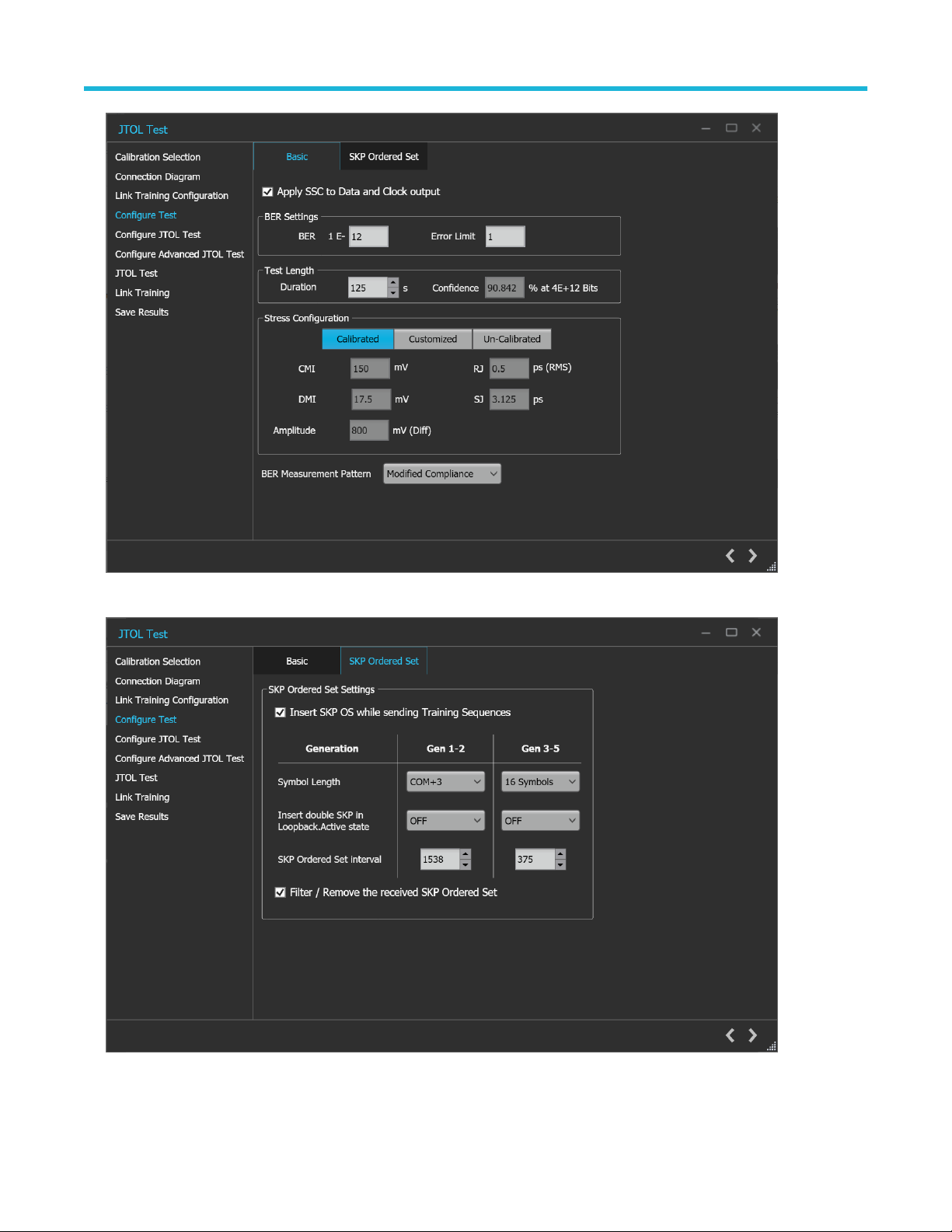
Operating basics
Figure 67: JTOL Test: Configure Test (Basic)
Figure 68: JTOL Test: Configure Test (SKP Orderd Set)
PCIe4.0 (CEM) Receiver Test Application Help 85
Page 86

Operating basics
Table 45: JTOL Test: Configure Test (Basic)
Parameter Description
BER Settings
• BER - Enter the number of bits in error that can be tolerated.
• Error Limit - Enter the required error limit. The default value is 1.
Test Length
Stress Configuration Select the required stress configuration among calibrated, customized, un-calibrated.
Spread Spectrum Clocking (SSC) Enables SSC for both Data and Clock
CMI Displays the CMI value in mV. The stress on the waveform is defined by the parameters
DMI Displays the DMI value in mV. The stress on the waveform is defined by the parameters
Amplitude Displays the Amplitude value in mV. The stress on the waveform is defined by the
RJ Displays the RJ value in ps or UIp-p. The stress on the waveform is defined by the
SJ Displays the SJ value in ps or UIp-p. The stress on the waveform is defined by the
BER Measurement Pattern Select the required BER measurement pattern from the drop-down list.
• Duration - Enter the test length duration value.
• Confidence - Displays the test length confidence value.
of CMI.
of DMI.
parameters of Amplitude.
parameters of RJ.
parameters of SJ.
Table 46: JTOL Test: Configure Test (SKP Order Set)
Parameter Description
SKP Ordered Set Settings
Insert SKP OS while sendingTraining Sequence Click to insert SKP OS while sending training sequence.
Symbol Length Select the required symbol length from the drop-down list for the
corresponding generation.
Insert double SKP in Loopback.Active state Select the required option (ON/OFF) from the drop-down list for
the corresponding generation.
SKP Orderd Set interval Select the required interval value from the drop-down list for the
corresponding generation.
Filter/Remove the received SKP Order Set Select to enable the filter or remove the received SKP ordered
set.
Click to move to the next screen.
5. Configure JTOL Test: This tab allows you to configure the JTOL test settings.
86
Page 87

Operating basics
Figure 69: JTOL Test: Configure JTOL Test
Table 47: JTOL Test: Configure JTOL Test
Parameter Description
Frequency Settings
Frequency (MHz) Displays the table of frequencies in MHz for which JTOL test is to be performed.
Lower Amplitude Limit (UI p-p) Displays the table of lower amplitude limit values at which JTOL test starts for that
frequency.
Higher Amplitude Limit (UI p-p) Displays the table of higher amplitude limit values at which JTOL test ends for that
frequency.
Min Frequency Enter the minimum frequency value.
Max Frequency Enter the maximum frequency value.
# Frequencies Enter the desired number of frequencies within the specified range.
Generate Click to view the table populated with the frequencies.
Default Click to view the table populated with default list of frequencies.
JTOL Custom Mask Select to enable the JTOL Custom mask.
On JTOL custom mask selection with the defined mask settings, mask will get generated
on the plot.
Table continued…
PCIe4.0 (CEM) Receiver Test Application Help 87
Page 88

Operating basics
Parameter Description
Mask Settings
Frequency (MHz) Displays the table of knee frequencies for the mask.
Amplitude (UI p-p) Displays the amplitude of SJ at each knee frequency.
Click to move to the next screen.
6. Configure Advanced JTOL Test: This tab allows you to configure the advanced JTOL test settings.
Figure 70: JTOL Test: Configure Advanced JTOL Test
Table 48: JTOL Test: Configure Advanced JTOL Test
Parameter Description
Relaxation Time Enter the amount of time BERT needs to relax before running BER for each amplitude
point.
Table continued…
88
Page 89

Operating basics
Parameter Description
Search Algorithms Select the required search algorithm from the drop-down for JTOL test.
• Binary
• Downwards Linear
• Downwards Log
• Upwards Log
• Upwards Linear
• Binary + Linear
Jitter Steps
Jitter Freq Range The different frequency ranges can have different step size for SJ amplitude sweep.
• Freq <= 100 KHz
• 100KHz < Freq <=1 MHz
• 1 MHz < Freq <=10 MHz
• 10 MHz <Freq <= 100 MHz
Step (UI p-p) Sets the SJ amplitude step size for different frequency ranges.
Sets the ratios for Downward and Upward-Log search algorithms.
No steps size is defined for Binary + Linear search algorithm.
Click to move to the next screen.
7. JTOL Test: This tab displays a graphical representation of JTOL test result. It includes the result table tab which displays the JTOL test
results in a tabular form.
PCIe4.0 (CEM) Receiver Test Application Help 89
Page 90

Operating basics
Figure 71: JTOL Test: JTOL Chart
Table 49: JTOL Test: JTOL Chart
Parameter Description
Units Select the required unit from the drop-down list. The list contains the following elements:
• ps
• UI
p-p
Start Click Start to run the test.
Skip Link Training Select if DUT is already in link.
90
Page 91

Operating basics
Figure 72: JTOL Test (Result Table)
Table 50: JTOL Test (Results Table)
Parameter Description
SJ Frequency (MHz) Displays the frequencies for which JTOL Test was performed.
SJ Setting (UI
Calibrated SJ (UI
#Errors Displays the Error count reported by MX183000A.
Click to move to the next screen.
8. Link Training:This tab displays the loopback steps with its status in a tabular form.
/ ps) Displays the SJ Amplitude on the BERT.
p-p
/ ps) Displays the Calibrated SJ Amplitude.
p-p
PCIe4.0 (CEM) Receiver Test Application Help 91
Page 92

Operating basics
Figure 73: JTOL Test: Link Training
Table 51: JTOL Test: Link Training
Parameter Description
Step Lists the different steps that are prerequisite for initiating link training
Status Indicates the completion status of each activity
Initialize Initialize the BERT for performing link training
Set Preshoot and deemphasis Sets the preset as per BERT Initial Preset in Link Training Configuration wizard
It sets all the calibrated Presets on the BERT from P0-P9
Setting Stresses Sets stresses as per the user selection in Configure Test wizard
Configure JTOL Test Sets the BERT, DUT initial and Target Presets, Loopback mode (Recovery, Config),
Link and Lane number
Link Training Initiates the link training process in MX 183000A
Click to move to the next screen.
9. Save Results: This tab allows you to save the JTOL test results.
92
Page 93

Operating basics
Figure 74: JTOL Test: Save Results
Table 52: JTOL Test: Save Results
Parameter Description
Unique ID Enter the Unique ID of the calibrated equipment in the text box.
Generated By Enter the user name in the text box.
Comments (Optional) Enter the required comments in the comment box.
Save Click to save the results.
Click to complete the JTOL Test and close the wizard.
PCIe4.0 (CEM) Receiver Test Application Help 93
Page 94

Programmatic interface commands
Programmatic interface commands
PREF:BERT:IP
This command sets or returns the IP address of the BERT used to connect with the PCIe4.0 (CEM) TekRxTest application.
Syntax
PREF:BERT:IP <IP address>
PREF:BERT:IP?
Inputs
<IP address> = <String>
Outputs
<String>
PREF:RTS:IP
This command sets or returns the IP address of the Real Time Oscilloscope used to connect with the PCIe4.0 (CEM) TekRxTest
application.
Syntax
PREF:RTS:IP <IP address>
PREF:RTS:IP?
Inputs
<IP address> = <String>
Outputs
<String>
CONN:BERT
This command sets or returns the connection status of the BERT with PCIe4.0 (CEM) TekRxTest application.
Syntax
CONN:BERT <0 | 1>
CONN:BERT?
Inputs
<0 | 1>
0 indicates to disconnect the BERT.
1 indicates to connect the BERT.
Outputs
<0 | 1>
94
Page 95

Programmatic interface commands
CONN:RTS
This command sets or returns the connection status of the Real Time Oscilloscope with PCIe4.0 (CEM) TekRxTest application.
Syntax
CONN:RTS <0 | 1>
CONN:RTS?
Inputs
<0 | 1>
0 indicates to disconnect the Real Time Oscilloscope.
1 indicates to connect the Real Time Oscilloscope.
Outputs
<0 | 1>
SETTINGS:RTS:POSITIVECHANNEL
This command sets or returns the real time scope channel number for positive channel.
Syntax
SETTINGS:RTS:POSITIVECHANNEL <0 | 1 | 2 | 3>
SETTINGS:RTS:POSITIVECHANNEL?
Inputs
<0 | 1 | 2 | 3>
0 - Indicates the CH1.
1 - Indicates the CH2.
2 - Indicates the CH3.
3 - Indicates the CH4.
Outputs
<0 | 1 | 2 | 3>
SETTINGS:RTS:NEGATIVECHANNEL
This command sets or returns the real time scope channel number for negative channel.
Syntax
SETTINGS:RTS:NEGATIVECHANNEL <0 | 1 | 2 | 3>
SETTINGS:RTS:NEGATIVECHANNEL?
Inputs
<0 | 1 | 2 | 3>
0 - Indicates the CH1.
1 - Indicates the CH2.
PCIe4.0 (CEM) Receiver Test Application Help 95
Page 96

Programmatic interface commands
2 - Indicates the CH3.
3 - Indicates the CH4.
Outputs
<0 | 1 | 2 | 3>
SETTINGS:RTS:SAMPLERATE
This command returns the sample rate of Real Time oscilloscope.
Syntax
SETTINGS:RTS:SAMPLERATE?
Inputs
NA
Outputs
<NRf>
SETTINGS:TEKRXSERVICE:ANALYSISTIMEOUT
This command sets or returns TekRxService analysis time out value.
Syntax
SETTINGS:TEKRXSERVICE:ANALYSISTIMEOUT<int>
SETTINGS:TEKRXSERVICE:ANALYSISTIMEOUT?
Inputs
<int> 15 to 1000
Outputs
<int>
SETTINGS:SIGTEST:VERSION
This command sets or returns the sigtest version number.
Syntax
SETTINGS:SIGTEST:VERSION <String>
SETTINGS:SIGTEST:VERSION?
Inputs
<String>
Outputs
<String>
SETTINGS:AMPLITUDE:TARGET
This command returns the nominal amplitude target value.
96
Page 97

Syntax
SETTINGS:AMPLITUDE:TARGET?
Inputs
NA
Outputs
<NRf>
SETTINGS:RJ:TARGET
This command returns the nominal RJ target value.
Syntax
SETTINGS:RJ:TARGET?
Inputs
NA
Outputs
Programmatic interface commands
<NRf>
SETTINGS:SJAT100MHZ:TARGET
This command returns the nominal SJ target value.
Syntax
SETTINGS:SJAT100MHZ:TARGET?
Inputs
NA
Outputs
<NRf>
SETTINGS:DMI:TARGET
This command returns the nominal DMI target value.
Syntax
SETTINGS:DMI:TARGET?
Inputs
NA
Outputs
<NRf>
PCIe4.0 (CEM) Receiver Test Application Help 97
Page 98

Programmatic interface commands
SETTINGS:CMI:TARGET
This command returns the nominal CMI target value.
Syntax
SETTINGS:CMI:TARGET?
Inputs
NA
Outputs
<NRf>
SETTINGS:MULTITONESJCAL:ENABLE
This command sets or returns the enable or disable status of Multi-tone SJ calibration.
Syntax
SETTINGS:MULTITONESJCAL:ENABLE {0|1}
SETTINGS:MULTITONESJCAL:ENABLE?
Inputs
{0 | 1}
0 indicates to disable the multi-tone SJ calibration.
1 indicates to enable the multi-tone SJ calibration.
Outputs
{0 | 1}
SETTINGS:MULTITONESJCAL:FREQUENCYCOUNT
This command sets or returns the frequency count value for Multi-tone SJ calibration.
Syntax
SETTINGS:MULTITONESJCAL:FREQUENCYCOUNT <NR1>
SETTINGS:MULTITONESJCAL:FREQUENCYCOUNT?
Inputs
<NR1> 1 to 14
Outputs
<NR1>
SETTINGS:MULTITONESJCAL:MAXFREQUENCY
This command sets or returns the maximum frequency value for Multi-tone SJ calibration.
Syntax
SETTINGS:MULTITONESJCAL:MAXFREQUENCY <NR1>
98
Page 99

SETTINGS:MULTITONESJCAL:MAXFREQUENCY?
Inputs
<NR1> 1 to 100 MHz
Outputs
<NR1>
SETTINGS:MULTITONESJCAL:MINFREQUENCY
This command sets or returns the minimum frequency value for Multi-tone SJ calibration.
Syntax
SETTINGS:MULTITONESJCAL:MINFREQUENCY <NR1>
SETTINGS:MULTITONESJCAL:MINFREQUENCY?
Inputs
<NR1> 0.03 to 99 MHz
Outputs
Programmatic interface commands
<NR1>
SETTINGS:MULTITONESJCAL:POINTS
This command sets or returns the number of points for Multi-tone SJ calibration.
Syntax
SETTINGS:MULTITONESJCAL:POINTS <NR1>
SETTINGS:MULTITONESJCAL:POINTS?
Inputs
<NR1> 2 to 8
Outputs
<NR1>
SETTINGS:EYE:ACQUISITIONS
This command sets or returns the number of acquisitions for stressed eye calibration.
Syntax
SETTINGS:EYE:ACQUISITIONS <int>
SETTINGS:EYE:ACQUISITIONS?
Inputs
<int> 1 to 20
Outputs
<int>
PCIe4.0 (CEM) Receiver Test Application Help 99
Page 100

Programmatic interface commands
SETTINGS:MULTITONESJCAL:DEFAULT
This command sets the SJ Frequencies to its default value for multitone SJ calibration.
Syntax
SETTINGS:MULTITONESJCAL:DEFAULT
Inputs
NA
Outputs
NA
SETTINGS:MULTITONESJCAL:GENERATE
This command generates the SJ frequencies for multitone SJ calibration.
Syntax
SETTINGS:MULTITONESJCAL:GENERATE
Inputs
NA
Outputs
NA
SETTINGS:SOCKETSERVER:IP
This command returns the IP address of the socket server.
Syntax
SETTINGS:SOCKETSERVER:IP?
Inputs
NA
Outputs
<String>
SETTINGS:SOCKETSERVER:LISTENINGPORT
This command returns the listening port of the socket server.
Syntax
SETTINGS:SOCKETSERVER:LISTENINGPORT?
Inputs
NA
Outputs
<String>
100
 Loading...