

Page 1
Package 82 Simultaneous CV
Instruction Manual
Chntains Operating Information
Publication Date: November 1968
Document Number: 5956-901-01 Rev. C
Page 2
WARRANTY
Keithley Instruments, Inc. warrants this product to be free from defects in material and
workmanship for a period of 1 year from date of shipment. During the warranty period, we
will, at our option, either repair or replace any product that proves to be defective.
To exercise this warranty, write or call your local Keithley representative, or contact Keithley headquarters in Cleveland, Ohio. You will be given prompt assistance and return instructions. Send the instrument, transportation prepaid, to the indicated service facility. Repairs will be made and the instrument returned, transportation prepaid. Repaired products
are warranted for the balance of the original warranty period, or at least 90 days.
LIMITATION OF WARRANTY
This warranty does not apply to defects resulting from unauthorized modification or misuse
of any product or part. This warranty also does not apply to fuses, batteries, or damage from
battery leakage.
This warranty is in lieu of all other warranties, expressed or implied, including any implied
warranty of merchantability or fitness for a particular use. Keithley Instruments, Inc. shall
not be liable for any indirect, special or consequential damages.
STATEMENT OF CALIBRATION
This instrument has been inspected and tested in accordance with specifications published
by Keithley Instruments, Inc.
The accuracy and calibration of this instrument are traceable to the National Bureau of Standards through equipment which is calibrated at planned intervals by comparison to certified standards maintained in the Laboratories of Keithley Instruments, Inc.
WEST GERMANY: Kdtldq lnrtrrrmcatr GmbIi / Hdglhok 5 / Mmtdwn 70 I O+3WlOOZ-O I T&C 32-12160 / Tel&~ &35Via?ZS9
GRBATBRlTAINz ~~~U/l~~Rod/~BabhinRG2ONL/o73cB6l287/T~817W/Tddueo13c86J665
FztANcE
-SC ~~~LntrW/A~Wet~/UOZMS~/P.o.BoxU9/UM)ANCcrinchmr
s- Kdtblq InrtmrmntlsA/~.4/3600
AUSTRIA
n-AL*
Keitblq -mUa SARL / 3 Alla du 10 Rue AmbmiseCrdzat / B. P. 60 I 91121 PahisuuKeda l+OllS 13.5 I T&x 600 933 / Tel&c 1-50117726
Kd~~CollnbH/~~huul2/A-l110~/~mp)~~UI/Tdac131671/TJdue~Om)8(JS97
Kdtblq lnstmmmta Sill I Wale B. N 4/A / 20145 Miho / 02420360 or 02-4136!540 / Tdefa 02.4121245’
Dubadaf / 014214444 / T&x 323 VT / Tdohrc 072%315%
I 01330.35333 / T&x 24 684 / Telfax 01&.3MOSZl
Page 3

Instruction Manual
Package 82
Simultaneous CV
@NW, Keithley Instruments, Inc.
Instruments Division
Cleveland, Ohio, U.S.A.
Document Number 5956901-01
Page 4

Hewlett-Packard is a registered trademark of Hewlett-Packard Company.
IBM and AT are registered trademarks of Internation Business Machines, Inc.
Page 5
SPECIFICATIONS
ANALYSIS CAPABILITIES
CONSTANTS: Flatband C and V
GRAPHICS:
Measured:
CaIcnIated: Interface Trap Density vs. Trap Energy
Threshold Voltage
Bulk Doping
Effective Oxide Charge
Work Function
Doping Type
‘Best Depth’
Simuitaneous C vs. Gate Voltage
High Frequency C vs. Gate Voltage
Quasistatic C vs. Gate Voltage
Conductance vs. Gate Voltage
Q/t Current vs. Gate Voltage
Quasistatic C and Q/t Current
vs. Delay Time
Doping vs. Depletion Depth
Depletion Depth vs. Gate Voltage
High Frequency l/C’ vs. Gate Voltage
Band Bending vs. Gate Voltage
High Frequency C vs. Band Bending
Quasistatic C vs. Band Bending
VOLTAGE MEASUREMENT
ACCURACY (1Year,18°-280C): *(O.QS% rdg + SOmV).
RESOLUTION: 1OmV.
TEMPERATURECOEFFICIENT (O"-180&2So~oC):
*(O.OOS% + 1mV)K.
HIGH FREQUENCY CAPACITANCE*
1ookHz:
RANGE LUTION i(%rdg+ pF)
mo PF
lMHz:
RANGE LUTION ff%rdg+ pR
~PP
SHUNT CAPACITANCE LOADING EFFECT 0.1% of reading
TEST VOLTAGE: 15mV mu f 10%.
TEST FREQUENCY TOLERANCE: *O.l%.
RESCh QYe~,18~-28~C) too-lS" L 28°-400CJ NOISE
10 a
looa
2nF
RESO- 11 Year, 18"-28°C) (0"-18' (t 28°400C) NOISE
10 fF 0.9 + 0.05
2nF loofF 1.4 + 0.5 0.14
additional error per 1OOpF load with equal shunt load on input
and output.
ACCURACY
0.7 + 0.05 0.03
0.9 + 0.5 0.08
ACCURACY
TEMPERATURE
COEFFICIENT
i (% rdgvc
TEMPERATURE
COERIClENT
k(% rd@l'C
0.03 2cafF
P-P
18ofF
18LMfF
P-P
4lmfF
QUASISTATIC CAPACITANCE*
RANGE LUTION
XIIJ PF
RESO- (1Year,18°-280C)
10 fF 1.0 + 0.1
1mfF
2nP
ACCURACY
rekdg + pm
0.8 + 0.2 (0.09% rdg + 0.13 pF) x
NOISE P-P
(typic&
(0.12% rdg + 0.13 pF) x
(100 mV/STEP V) + 0.01 pF
(100 mV/STEP V) + 0.1 pF
VOLTAGE SOURCE
VOLTAGE (0.1 Hz to 10 Hz) RESOLUTION
S2OV
>iuvtol2ov
ll)@ally 3 mV up to 75 MHz.
MAXIMUM SWEEP SPAN, 1 V,,, - V,r 1: 40V.
MAXIMUM OUTPUT CURRENT: f2mA (-0%. +a%).
SWEEP STEP VOLTAGE SELECMONS: lOmV, 2OmV, SOmV,
1OOHlV.
DC OUTPUT RESISTANCE: Clof.2.
P-PNOISE'
EJl rv
23 rv
10 mV
100 mV
GENERAL
RE&NfN~TES: 444 readings per second to one reading every
DATA BUFFER: 1000 points maximum.
GRAPHICAL OUTPUTS: Computer display or digital plotter
supporting HPGL with IEEE-488 interface; also “screen copy”
to compatiiIe printer.
DIGITAL I/O: Consists of one output, four inputs, +5V (series
limited with 33Q), and COMMON referenced to IEEE-W
COMMON. Output will drive one TI’L load. Inputs represent
one TIL load.
MAXIMUM INPUT: 30V peak, dc to 6oHz sine wave.
MAXIMUM COMMON MODE VOLTAGE: 3OV maximum, dc
to 6OHz sine wave.
OPERATING ENVIRONMENT:
densing RH up to 35°C.
STORAGE ENVIRONMENT: -29’ to +65X
O” to 40°C, 70% non-con-
TEMPERATURECOEFFICIENT @"-lt30&2W'-400C):
*(0.02% rdg + 0.1 pF)K.
*NOTES
Specifkationa are based on parallel RC model and Quality Factor s 20.
Assumes pfopa cable cone&on and open circuit suppression.
~~capsdturerruracyisexdusivcofnoise,for~VrO.OSV
and DEUY TIME s 1 second. For other parameters, derate by
(SmV/STEP V) x (DELAY TIME/l second) in pF at 23OC. Double the
derating for every 10°C rise in ambient temperature above 23°C.
l)pical allowable noniquilbrium current plus leakage current: <ZOpA
on ZOOpF range; cZOOpA on 2nF range during capacitance measurements.
WARMUP: 2 hours to rated accuracy.
SYSTEM CONFIGURATION: Models 22&l, 590,595, and 5951
connected as shown in manual. Controller is HP Series 200 or
300 with BASIC 4.0. Requires 1 Mbyte of memory.
PACRAGE 82 COMPONENTS:
ModeI 230-k Prognmnublc Voltage Source
Model 595:
Model 590:
Model 5909: Calibration Sources
Model 5956:
Model 5951:
Spe&cationa subject to change without notice.
Quaiatatic cv Meter
look/lMcv‘4nalyBer
Packa@? 82 CV Software and Manual
Remote Input Coupler-Includes Models:
Low Noise BNC Cable, 1.2m (4 ft.) (5 supplied)
rllwI1:
7OW1: Shielded IEEEaB Cable, Im (3.3 ft.) (2 supplied)
7007-2: Shielded IEEE488 Cable, Zm (6.6 ft.) (1 supplied)
7051-2: RG-58C BNC to BNC Cable, 0.6m (2 ft.) (3 supplied)
Page 6

Contains information on Package 82 features, specifi-
cations, and supplied accessories.
Gives information to aid in getting your simulta-
neous CV system up and running as quickly as
possible, including hardware and software configuration.
Covers detailed operation including system calibration, correction, and taking data.
SECTION 1 1
General Information j
SECTION 2
Getting Started
SECTION 3 1
Measurement /
Details analysis functions of the Package 82.
Discusses system block diagram, the remote input
coupler, and quasistatic and high-frequency CV
principles.
SECTION 4
SECTION 5
Principles of Operation
Page 7
Table of Contents
SECTION l-GENERAL INFORMATION
1.1
1.2
1.3
1.4
5
i-L
ii2
1.8
1.9
1.9.1
1.9.2
1.10
INTRODUCT’ION ...............................
FEfmJREs
WARRANTY INFORMATION
MANUAL ADDENDA
sm SYMBOLS AND TERMS
SPECIFICAI'IONS
UNPACKING AND INSPECTION
Unpa~gPK>cedure
SuppiiedEquipment
REFACKING FOR SHIPMENT
COMPUTER CONFIGURATION
Series 200 and 300
IBM AT
SERVICE AND CALIBRATION.
...............................
...................................................................
..........................................................................
..............................................................................
.........................................................................
............................................................................
...........................................................................
.....................................................................................
SECTION P-GETTING STARTED
..............................................................................
........................................................................
.:
....
..........................................................................
....................................................................
....................................................................
...........................................................................
...........................................................................
.....................................................................
.............................................................................
.........................................................................
..............................................................................
...........................................................................
.............................................................................
.................................................
...............................................................................
........................................................................
................................................................................
......................................................................
............................................................................
.........................................................................
...................................................................
.........................................................................
.........................................................................
......................................................................
..................................................................................
............................................................................
..........................................................................
i-:.
2:2.1
2.2.2
2.2.3
2.2.4
2.2.5
2.3
2.3.1
2.3.2
2.3.3
2.3.4
2.3.5
2.3.6
2.4
2.4.1
2.4.2
2.4.3
2.4.4
El
2:5:2
2.5.3
2.5.4
2.5.5
2.5.6
2.6
2.6.1
2.6.2
2.7
2.7.1
2.7.2
2.7.3
2.7.4
INTRODUCI’ION
HARDWARE CONFIGURATION
SystemBlockDiagram
RemoteInputCoupler..
SystemConnections
IEEE-483 Bus Connections
Remote Coupler Mounting
SYSTEM POWER UP
Instrument Power Requirements
Power Connections
Environmental Conditions
Warm Up Period
Power Up Procedure
Line Frequency
SOFTWARE CONFIGURAl’ION
Computer Boot Up
Software Backup
Software Initialization
Software Files
SOFIWARE OVERVIEW
System Reset
System Characterization
Cable Correction
C& and Delay Time Determination
Device Measurement
Data Analysis and Plotting
SYSTEM CHECKOUT
Checkout Procedure
System Troubleshooting
USING THE PACKAGE 82 WITH THE IBM AT
Installation
Software Backup
Configuration File Modification
Booting the System
...............................................
.....................................................
...............................................................
...............................................................
..................................................................
................................................................
.................................................................
................................................................
................................................................
...............................................................
.................................................................
............................................................
..................................................
...............................................................
l-1
l-l
l-l
l-1
l-l
l-2
l-2
l-2
l-2
l-2
l-2
l-2
l-2
2-1
2-l
2-l
2-l
2-4
2-6
2-6
2-7
2-7
2-7
2-7
2-a
i:
2-9
2-9
2-9
..- .................... 2-9
;I;
2-9
2-9
2-10
2-11
2-n
2-U
2-11
2-n
2-ll
;I:
2-33
2-l3
2-B
i
Page 8

2.7.5
.......................................................................................................
27.6
Modifyingtheprintpath...................................... . . . . . . . . . . ..*......*........a..
Operational Check. . . . . . .
SECTION 3--MEASUREMENT
. . . . . . . . . . . . . . . . . . ..*............................*.............*....
2-14
2-14
3.1
3.2
3*3
3.4
3.4.1
3.4.2
3.4.3
3.4.4
3.45
3.5
3.5.1
3.5.2
3.5.3
3.54
3.5.5
3.5.6
3.6
3.6.1
36.2
3.6.3
3.6.4
El
3?2
3.7.3
37.4
37.5
3.8
38.1
38.2
3.8.3
3.9
3.9.1
3.9.2
3.9.3
3.9.4
3.9.5
INTRODUCTION
MEASUREMENT SEQUENCE
SYSTEM RESET
TESTING AND CORRECTING FOR SYSTEM LEAKAGES AND !XFWt’S
Test and Correction Menu
.............................................................................. 3-l
...................................................................
...............................................................................
...........................
....................................................................
Parameter Selection
Viewing Leakage Levels
System Leakage Test Sweep
Offset Suppression
CORRECT’ING FOR CABLING EFFECTS
When to Perform Cable Correction.
RecommendedSources
Source Connections
.........................................................................
~oha.re Mciiflcation
Y **
Correction Procedure
Optimizhg Correction Accuracy to Probe Tips
.................................................................................................................................................
...........................................................................................................................................
..
........................................................
...........................................................
......................................................................
.........................................................................
........................................................................
.................................................
DETERMNNG OXIDE CAPACTIXNCE AND EQUILIBRIUM DELAY TIME
& and Delay Time Menu
Running and Analyzing a Diagnostic CV Sweep
...... .... .. .
........... ........
..........
Determining Oxide Capacitance, Oxide Thickness, and Gate Area
Determining Optimum Delay lime
MAKINGCVMF&lIGMEMS
CVMeasurementMenu
....
...........................................................
...............................................................
........................................................................................................................
Programming Measurement Parameters
Manual CV Sweep
......................................................................................................................................................
Auto CV Sweep
Using Corrected Capacitance
LIGHT CONNECX’IONS
Digital I/O Port Tixminals
LED collnectioIls
...........................................................................
Relaycontrol.......................................~
MEASUREMENT CDNSID~ONS
Potential Error Sources
AvoidmgCapacitanceEm>rs
Correcting Residual Errors
Interpreting CV Curves
DynamicRangecOnsideratio~
.................................................................
......................................................................
....................................................................
.......................................
................................................
......................................................................
........
1.
.................................................................
...................................................................
......................................................................
...............................................................
........................
3-3
3-3
g
3-9
3-13
3-13
3-13
3-h
r) -se
zfi
346
3-16
3-X
3-18
3-20
3-22
3-26
322
3-29
3-30
3-33
3-33
3-33
3-34
3-34
g;
3-z
3-39
3-40
SECTION 4-ANALYSIS
4.1
4.2
4.21
INTRODUCTlON
CONSWNTS AND SYMBOLS USED FOR ANALYSIS
constants.
4.2.2 Raw Data Symbols
42.3
4.3
4.3.1
4.3.2
4.4
44.1
4.4.2
Calculated Data Symbols
OB’UINNG IN-FOlWiAIlON FROM BASIC CV CURVES
Basic CV Curves
Dgtermining Device~e
ANAIXING CV DAIX
PlotterandPxinter Requirements..
Analysis Menu
ii
..............................................................................
.....
..
..........
...........................................................................
....... .....
..................................................................................................
.....................................................................
.............................................................................
.....................................................................
........................................................................
............................................................
..............................................................................
.........................................
41
E;
41
42
42
42
44
44
4-4
45
Page 9
4.4.3
4.4.4
4.4.5
4.4.6
4.4.7
4.4.8
4.4.9
4.4.10
4.4.11
4.4.12
4.4.13
4.4.14
4.5
4.5.1
4.5.2
4.5.3
4.6
4.6.1
4.6.2
Saving andRecalling Data
Displaying and Printing the Reading and Graphics Arrays
Graphing Data
AnalysisTools .............................................................................. 410
Reading Array
Calculated Data Array (Graphics Array)
Constants Used for Analysis
Graphing the Reading Array
Doping Profile
Flatband Capacitance
Interface Trap Density Analysis.
CalculatedAccuracyofNandD~.
MOBIL,E IONIC CHARGE CONCENTTWHON MEASUREMENT .................................
Flatband Voltage Shift Method.
Triangular Voltage Sweep Method
Using Effective Charge to Determine Mobile Ion Drift
REFERENCES AND BIBLIOGRAPHY OF CV MEASUREMENTS AND RELAI’ED TOPICS.
References
Bibliography of CV Measurements and Related Topics
..............................................................................
.............................................................................. 412
..............................................................................
.................................................................................
...................................................................
.................................................................
.................................................................
.......................................................................
.............................................................
...........................................................
..............................................................
........................................................... 430
SECTION 5-PRINCIPLES OF OPERATION
......................................
......................................................
......................................... .433
.........................................
.........
4-6
46
49
413
413
413
419
423
4-23
429
429
4-29
433
433
433
................................................. ............................ 5-l
...................................................................
...................................................................
..............................................................................
........................................................................... 5-2
............................................................................
.................................................................
.......................................................................
.......................................................................
............................................................... 5-5
..........................................................................
::1
El
5:3:2
5.4
5.4.1
5.4.2
5.5
5.5.1
5.5.2
5.6
INTRODUCTION
SYSTEM BLOCK DIAGRAM
REMOTE INPUT COUPLER
Tuned Circuits
Frequency Control
QUASISTATIC CV.
Quasistatic~ Configuration
Measurement Method
HIGH FREQUENCY CV
High Frequency System Configuration
High-Fluency Measurements
SIMUJXWEOUS CV
SECTION 6-REPLACEABLE PARTS
6.1
6.2
E
k5
INTRODUCT’ION
Pm LIST ..................................................................................
ORDERING INFORMAlTON
FACRJRY SERVICE ...........................................................................
COMPONENT LAYOUTS AND
................................................. ............................
........................................ ...........................
s
CHEMAX DIAGRAMS
APPENDICES
Appendix A
Appendix B
Appendix C
AppendixD ..................................................................................
Appendix E
AppendixF
..................................................................................
..................................................................................
..................................................................................
..................................................................................
...................................................................................
........................................................
........................................ 6-l
5-l
5-2
5-2
5-3
5-3
5-3
53
5-5
5-6
:;
z
A-l
g:1
D-l
E-l
F-l
iii/iv
Page 10
List of Illustrations
SECTION 2-GETTING STARTED
2-l
2-2
2-3
2-4
2-5
2-6
2-7
2-8 Main Menu.
System BlockDiagram
Model5951 Front Panel
Model 5951RearPanel
System Front Panel Connections
System Rear Panel Connections
System IEEE-488 Connections
Remote Coupler Mounting
..................................................................................
.........................................................................
........................................................................
.........................................................................
SECTION 34blEASUREMENT
3-l
3-2
3-3
2
3-6
3-7
3-8
3-9
3-10
3-11
3-22
3-13
3-14
3-15
3-16
3-v
3-18
3-19
3-20
3-21
3-22
3-23
3-24
3-25
3-26
3-27
3-28
3-29
3-30
3-31
3-32
3-33
3-34
3-35
3-36
Measurement Sequence
Package 82 Main Menu
Stray Capacitance and Leakage Current.
Parameter Selection Menu
Save/Load Parameter Menu
Monitor Leakage Menu
Diagnostic Sweep Menu
Leakage Due to Constant Current
Q/t Curve with Leakage Resistance
Constant Leakage Current .Increases*Quasistatic Capacitance
Quasistatic Capacitance with and without Leakage Current
Cable Correction Connections
Partial Listing Showing Nominal Source Values
X and Delay Time Menu
co
CV Characteristics of n-type Material
CV Characteristics of p-type Material
Oxide Capacitance Menu
Delay Time Menu
Q/t and C, vs. Delay Time Fixample
Choosing Optimum Delay Time
Capacitance and Leakage Current Using Corrected Capacitance
Device Measurement Menu
Parameter Selection Menu
Manual Sweep Menu
Auto Sweep Menu
Digital 110 Port Terminal Arrangement
Direct LED Control
Relay Light Control
CV Curve with Capacitance Offset
CV Curve with Added Noise
CvCurw Resukingfrom GainError
Curve Tilt Caused By Voltage-dependent Leakage
W Curve Caused By Nonlinearity
Normal~CurveRes&swhenDeviceisKeptinEquiBbrium..
Curve Hysteresis Resulting When Sweep is Too Rapid
DistortionWhenHoldTieisTooShort..
........................................................................
.........................................................................
.........................................................................
.......................................................................
.............................................................................
.........................................................................
............................................................................
...........................................................................
...........................................................................
................................................................
.................................................................
....................................................................
......................................................................
.........................................................
......................................................................
.....................................................................
..............................................................
.............................................................
...................................... 3-12
.......................................
...................................................................
..................................................
.....................................................................
........................................................... 3-19
...........................................................
......................................................................
............................................................
................................................................
...................................
....................................................................
.....................................................................
..........................................................
.............................................................
..................................................................
...........................................................
................................................
.............................................................
..................................
...........................................
......................................................
2-2
2-2
2-3
2-5
2-5
2-6
2-7
2-10
3-l
3-3
3-4
3-5
3-7
3-9
3-11
3-12
3-32
3-12
3-14
3-15
3-17
3-20
3-21
3-23
3-24
3-25
3-25
3-27
3-28
3-31
3-32
3-33
3-34
3-35
3-35
3-36
3-36
3-36
3-37
3-39
3-41
3-41
V
Page 11
SECTION 4-ANALYSIS
41
42
2
45
2
4-8
4-9
410
Q-11
PI2
413
414
4-15
4-16
417
418
4l9
420
42l
CV Characteristics of p-type Material
CV Characteristics of n-type Material
Data Analysis Menu
........................................................................... z
Example of Reading Array Print Out
Example of Graphics Array Print Out
Graphics Control Menu
Reading Array
Graphics &ray
...............................................................................
............................................................................... 423
....................................................................... 49
Quasistatic Capacitance vs. Gate Voltage Example (Normalized to Lx)
High-Frequency vs. Gate Voltage Example (Nonnaked to 6x)
High-Frequency and Quasistatic vs. Gate Voltage Example
Q/t vs. Gate Voltage Example
..................................................................
Conductance vs. Gate Voltage Example
Depth vs. Gate Voltage Example
Doping Profile vs. Depth Example
Kh’ vs. Gate Voltage Example
Band Bending vs. Gate Voltage Example
Quasistatic Capacitance vs. Band Bending Example
Hligh~FrequencyCapacitance vs Band Bending Examp!e
Interface Trap Density vs. Energy from Midgap Example
Model for TVS Measurement of Oxide Charge Density
...........................................................
...........................................................
............................................................
........................................................... z
.........................................................
............................................................... 420
............................................................. 421
................................................................ 422
....................................................... 425
SEaION S-PRINCIPLES OF OPERATION
5-l
z
5-4
5-5
5-6
El
System Block Diagram
Simplified Schematic of Remote Input Coupler
System Configuration~for Quasistatic CV Measurements
Bxdbaclc Charge Method of Capacitance Measurements
U&age and Charge Waveforms for Quasistatic Capacitance Measurement
System Configuration for High Frequency CV Measurements
High Frequency Capacitance Measurement
Simukmeous CV Waveform.
.........................................................................
...................................................................
............................
................................... 415
....................................... 4%
.............................................
....................................
....
........................................
.......................................... 431
.................................................. 5-2
..........................................
..........................................
..........................
..................................... 5-5
......................................................
43
423
414
417
418
426
A-w
T”
428
5-l
5-3
54
5-4
5-6
57
vi
Page 12

List of Tables
SECTION l-GENERAL INFORMATION
l-1
l-2
l-3
SuppliedEquipment ...........................................................................
Minimum Computer Requirements ..............................................................
Necessary Binary Files
................................................ ..........................
SECTION 2-GETTING STARTED
2-l
;I$
Supplied Cables
Diskette Files
System Troubleshooting Summary
...............................................................................
.................................................................................
SECTON 3-MEASUREMENT
3-l
3-2
Cable Correction Sources
Digital I/O Port Terminal Assignments
......................................................................
SECTION 4-ANALYSIS
41
42 Displayed Constants
43 Analysis Constants
Graphical Analysis
............................................................................ 410
........................................................................... 4-10
............................................................................ 419
..............................................................
.......................................................... 3-33
l-3
l-3
l-3
2-4
;I;
3-14
vii/viii
Page 13

SECTION 1
’ General Information
1.1 INTRODUCTION
This section contains overview information for the Package
82 Simultaneous CV system and is arranged as follows:
1.2 Features
1.3 Warranty Information
1.4 Manual Addenda
1.5 Safety Symbols and Terms
Specifications
1.6
1.7 Unpacking and Inspection
Repacking for Shipment
1.8
1.9 Computer Configurations
Service and Calibration
1.10
1.2 FEATURES
The Package 82 is a computer-controlled system of instruments designed to make simultaneous quasistatic CV
and high frequency (1oOkHz and lMHz) CV measurements
on semiconductors. The package 82 includes a Model 590
CV Analyzer for high-frequency CV measurements, and
a Model 595 Quasistatic CV Meter, along with the
necessary input coupler, connecting and control cables,
and cable calibration sources. A Model 230-l Lbltage Souse
and software for the HP 9000 Series 2(Xl and 300 computers
(or an IBM AT with an HP BASIC language processor card)
running BASIC 4.0 are also included.
l Graphical analysis capabilities allow plotting of data on
the computer display as well as hard copy graphs using
an external digital plotter. Graphical analysis for such
parameters as doping profile and interface trap density
vs. trap energy is provided.
. Supplied external voltage source (Model 230-l) extends
the DC bias capabilities to *l2OV.
0 Supplied calibration capacitors to allow compensation for
cable effects that would otherwise reduce the accuracy
of lOOkHz and lMHz measurements.
l All necessary cables are supplied for easy system hook
UP.
1.3 WARRANTY INFORMATION
Warranty information is located on the inside front cover
of this instruction manual. Should you require warranty
service, contact your Keithley representative or the factory
for further information.
1.4 MANUAL ADDENDA
Any improvements or changes concerning the Package 82
or this instruction manual will be explained on a separate
addendum supplied with the package. Please be sure to
note these changes and incorporate them into the manual
before operating or servicing the system.
Key Package 82 features include:
0 Remote input coupler to simplify connections to the
device under test. Both the Model 595 and the Model
590 are connected to the device under test through the
coupler, allowing simultaneous quasistatic and high frequency measurement of device parameters with negligible interaction between instruments.
l Supplied menu-driven software allows easy collection
of C, G, V, and Q/t data with a minimum of effort. No
computer programming knowledge is necessary to
operate the system.
l Data can be stored on disk for later reference or analysis.
Addenda concerning the Models 250~1,590,595, and 5909
will be packed separately with those instruments.
1.5 SAFETY SYMBOLS AND TERMS
The following safety symbols and terms may be found on
one of the instruments or used in this manual:
symbol on an instrument indicates that you
Q
The ’
should consult the operating instructions in the associated
manual.
l-l
Page 14
GENERAL INFORMATION
The WARNING heading used in this and other manuals
cautions against possible hazards that could lead to personal injury or death. Always read the associated information very carefully before performing the indicated
procedure.
A CAUTION heading outlines dangers that could damage
the instrument. Such damage may invalidate the warranty.
1.6 SPECIFICATIONS
Detailed specifications for the Package 82 system can be
found at the front of this manual. Specifications for the
individual instruments are located in their respective instruction manuals.
1.7 UNPACKING AND INSPECTION
1.7.1 Unpacking Procedure
Upon receiving the Package 82, carefully unpack all instruments and accessories from their respective shipping
cartons, and inspect all items for any obvious physical
damage. Report any such damage to the shipping agent
at once. Save the original packing cartons for possible
future reshipment.
l Advise as to the warranty status of the equipment.
l Write ALTENTION REPAIR DEPARTMENT
on the ship
ping label.
l Fill out and include the service form which is located
at the back of this or one of the other instruction
manuals.
1.9 COMPUTER CONFIGURATIONS
1.9.1 HP Series 200 and 300
The Package 82 is supplied with software intended for use
with the Hewlett Packard HP 9000 Series 200 and 300 computers running under BASIC 4.0. Table l-2 summarizes
minimum requirements for the computer system. Table l-3
summarizes necessary binary files.
1.9.2 IBM AT
The Package 82 can also be used with an IBM AT (or com-
patible) that is equipped with a BASIC-ROM configured
HP-8232lA Language Processor card. Paragraph 23 of this
manual gives an overview of the procedure; see the HP
documentation for detailed information.
1.10 SERVICE AND CALIBRATION
1.7.2 Supplied Equipment
Table l-l summarizes the equipment supplied with the
Package 82 system.
1.8 REPACKING FOR SHIPMENT
Should it become necessary to return any of the instruments for repair, carefully pack them in their original
packing cartons (or the equivalent), and be sure to include
the following information:
The Model 5951 Remote Input Coupler cannot be
calibrated or repaired by the user, so it must be returned
to the factory or authorized service center for repair or
calibration. If the Model 5951 is to be returned, proceed
as folIows:
1. Complete the service form at the back of the manual
and include it with the unit.
2. tZarefdy pack the unit in the original packing carton
or its equivalent.
3. Write AITENTION RJBUR DEl?A#IuENT
on the ship
ping label.
l-2
Page 15
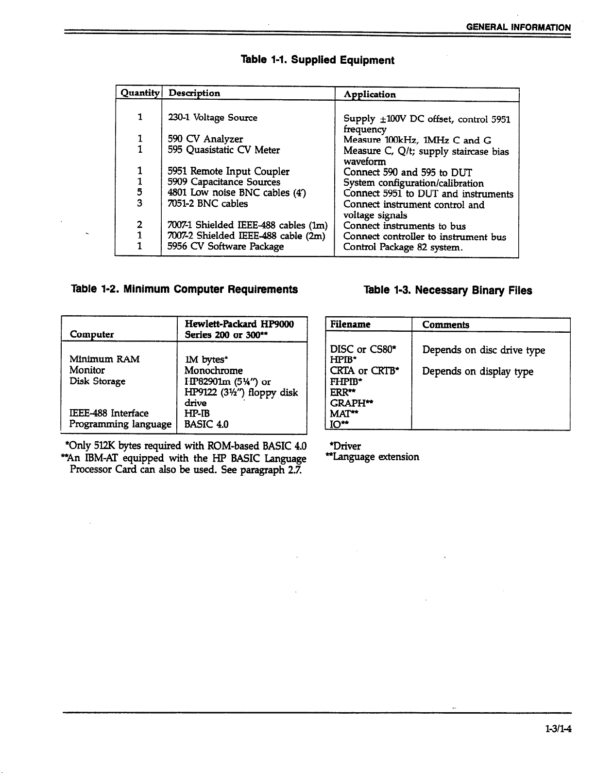
Table l-1. Supplied Equipment
GENERAL INFORMATION
w-------2
1
1
1
1
- ---- ----_
230-l Voltage Source
590 CV Analyzer
595 Quasistatic CV Meter
5951 Remote Input Coupler
5909 Capacitance Sources
:
3
.
2
1
1
4801 Low noise BNC cables (4’)
7051-2 BNC cables
7007-l Shielded IEEE488 cables (lm)
7007-2 Shielded IEEE488 cable (2m) Connect controller to instrument bus
5956 CV Software Package Control Package 82 system.
Table l-2. Minimum Computer Requirements
Hewlett-Packard HP9000
Computer
Minimum FUM
Monitor
Disk Storage
Series 200 or 300**
lM bytes*
Monochrome
HP829Olm (5%“) or
HP&TJ22 (3%“) floppy disk
IEEE-488 Interface
HP-I-B
Programming language BASIC 4.0
-Yp*.~.I”‘.
Supply *lOOV DC offset, control 5951
frequency
Measure lOOkI-&, lMHz C and G
Measure C, Q/t; supply staircase bias
waveform
Connect 590 and 595 to DUT
System configuration/calibration
Connect 5951 to DUT and instruments
Connect instrument control and
voltage signals
Connect instruments to bus
Table 1-3. Necessary Binary Files
Filename
DISC or CS80*
Comments
Depends on disc drive type
I-FIB*
CRTAorCRTB*
Depends on display type
FHPlB*
F!!KHW
IO”
*Only 5I2K bytes required with ROM-based BASIC 4.0
“An IBM-AT equipped with the HP BASIC Language
Processor Card can also be used. See paragraph 2.7.
*Driver
*Language extension
l-311-4
Page 16

SECTION 2
Getting Started
2.1 INTRODUCTION
Section 2 contains introductory information to help you get
your system up and running as quickly as possible. Section 3 contains more detailed information on using the
Package 82 system.
Section 2 contains:
2.2
Hardware Configuration: Details system hardware
configuration, cable co~ections, and remote input
coupler mounting.
2.3
System Power Up: Covers the power up procedure for
the system, environmental conditions, and warm up
periods.
2.4
Software Configuration: Outlines methods for
booting up the computer, making backup copies, and
Package 82 software initialization.
25
Software Ovmiew: Descriks the purpose andoverall
confi8uration of the Package 82 software
2.6
System Checkout: Gives the procedure for checking
out the system to ensure that everything is working
properly.
2.2 HARDWARE CONFIGURATION
The system block diagram and connection procedure are
covered in the following paragraphs.
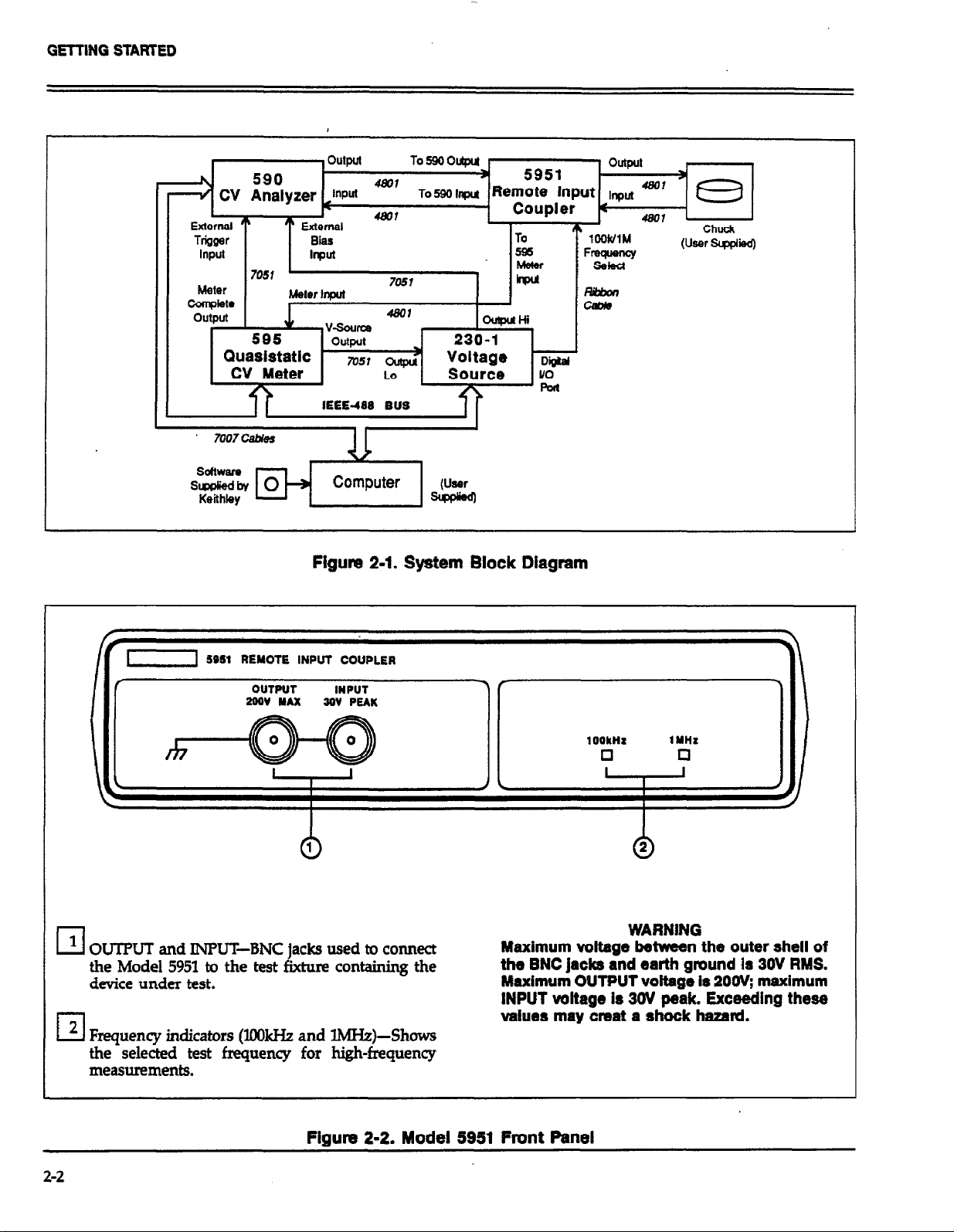
2.2.1 System Block Diagram
An overall block diagram of the Package 82 system is shown
in Fii 2-l. The function of each instrument is as follows:
Model 230-l Voltage Source-Supplies a DC offset voltage
of up to ~XHJV, and also controls operating frequency of
the Model 5951 Remote Input Coupler.
Model 590 CV Analyzer-Supplies a lCHWIz or lMHz test
signal and measures capacitance and conductance when
making high-frequency CV measurements.
Model 595 CV Meter-Measures low-frequency (quasistatic)
capacitance and Q/t, and also supplies the stepped bias
waveform (&2CW maximum) for simultaneous low- and
high-frequency CV measurement sweeps.
Model 5951 Remote Input Coupler-Connects the Model
590 and 595 inputs to the device under test. The input
coupler contains tuned circuits to minimize interaction between low- and high-frequency measurements.
Computer (HP 9000)-Provides the user interface to the
system and controls all instruments over the IEEE-488 bus,
processes data, and allows graphing of results.-
Model 5909 Calibration Set-Provides capacitance reference
somces for cable correcting the system to the test fixture.
2.2.2 Remote Input Coupler
The Model 5951 Remote Coupler is the link between the
test fixture (which contains the wafer under test) and the
measuring instruments, the Models 590 and 595. The unit
not only simplifies system connections, but also contains
the circuitry necessary to ensure minimal interaction between the low-frequency measurements made by the Model
595, and the high-frequency measurements made by the
Model 590.
The front and rear panels of the Model.5951 are shown in
Fiis 2-2 and 2-3 respectively. The front panel includes
input and output jacks for connections to the device under
test, as well as indicators that show the selected test frequency (l00kHz or lMI-Iz) for high-frequency measurements. The rear panel includes a binding post for chassis
ground, BNC jacks for connections to the Models 590 and
595, a ribbon cable connector (which co~ects to the Model
230-l digital I/O port), and a digital I/O port edge co~ec-
tar providing one ITL output, four TIL inputs, digital common, and +5V DC.
2-l
Page 17
GETTING STARTED
Meter
7051 ’
‘I ,-
c!cmdElta
I I
Meter Input
IEEE-48S BUS
7051
1 I
I
1
Figure 2-l. System Block Diagram
1 SOS1 REMOTE INPUT COUPLER
f
OUTPUT INPUT
2oov MAX 3oV PEAK
Tf
h5qHp
l
I
’ OUTPUT and INPU’LBNC jacks used to connect
cl
the Model 5951 to the test fixture containing the
device under test.
(7 2 Frequency indicators (X&Hz and lMHz)-Shows
the selected test frequency for high-frequency
measurements.
Figure 2-2. Model 5953 Front Panel
2-2
1 OQkHI
0
I
Maximum voltage between the outer shell of
the EJNC jacks and earth ground Is 3OV RMS.
Maximum OUTPUT voltage Is 200& maximum
INPUT voltage Is 30V peak. Exceeding these
values may &eat a shock hazard.
IYHt
cl
I
I
WARNING
)
-
Page 18
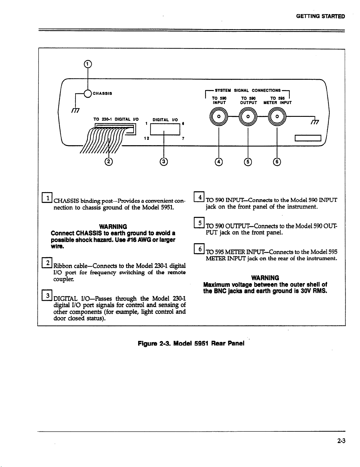
SYSTEM SIGNAL CONNECTIONS
GETTING STARTED
TO 2361 DIGITAL L’O
1
0
CHASSIS binding post-Provides a convenient connection to chassis ground of the Model 5951.
WARNING
Connect CHASSIS to earth ground to avoid a
possible shock hazard, Use #16 AWG or larger
Wh.
2 Ribbon cable-Connects to the Model 230-l digital
Ll
I/O port for frequency switching of the remote
coupler.
3 DIGllAL I/O-Passes through the Model 230-l
LJ
digital I/O port signals for control and sensing of
other components (for example, light control and
door closed status).
DIGITAL l/O
4 To 590 INPUT-Connects to the Model 590 INPUT
cl
jack on the front panel of the instrument.
5 ‘IO 590 OUTPUT-Connects to the Model 590 OUT
cl
PUT jack on the front panel.
6 To 595 METER INPUT-Connects to the Model 595
cl
METER INPUT jack on the rear of the instrument.
WARNING
Maximum voltage between the outer shell of
the BNC jacks and earth ground is 30V RYS.
Figure 2-3. Model 5951 Rear Panel ”
2-3
Page 19
GETTING STARTED
Table 2-l. Supplied Cables
-;
Q
5
3
2
1
1
Model
4801
7051-2
7N%l
7007-2
*
Description
4’ BNC Low Noise
Auriiication
590, 595, 5951
2’ BNC (RG-58) 230-1, 590, 595
lm shielded IEEE-488
IEEE-488 instrument bus
2m shielded IEEE-488 Computer to instruments
Ribbon cable 5951 to 230-l
*Supplied with Model 5951
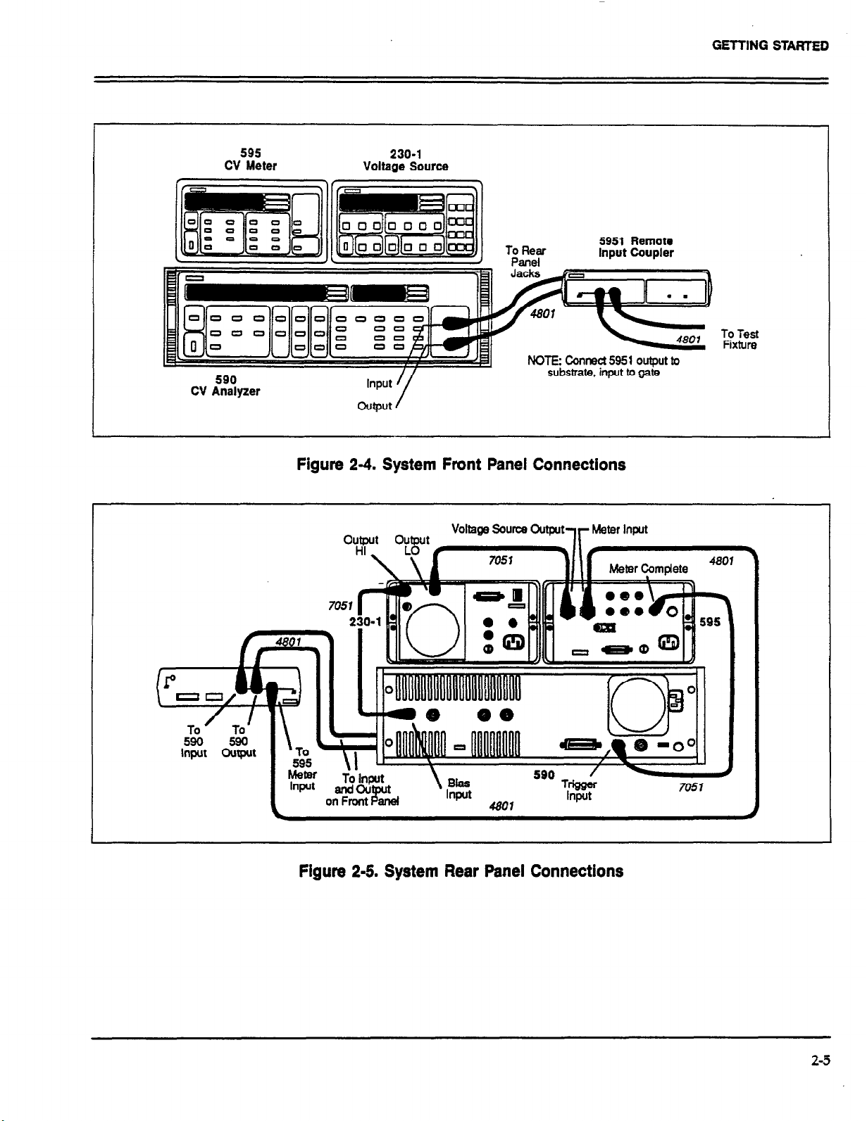
2.2.3 System Connections NOTE
OUTPUT should be connected to the substrate
Supplied Cables
lhble 2-l summarizes the cables supplied with the Package
82 system along with the application for each cable. Note
that low-noise cables am provided for making co~ections
between the chuck and the CV measurement instruments.
The Model 4801 cables are each four feet long. Be careful
not to use the Model 7051 BNC cables in place of the lownoise cables (Model 48Ol), as doing so will have detrimental effects on your measurements.
Connection Procedure
Use Figures 2-4 and 2-5 as a guide and co~ect the equip-
ment together as follows. Note that the stacked arrangement shown in the figures is recommended, but other
setups can be used, if desired.
NOTE
All equipment should be turned off when making coMections.
contact, and INPUT should be connected to the
gate metallization contact.
3. Connect the Model 5951 To 595 METER INPUT jack to
the Model 595 METER INPUT jack using a Model 4801
cable.
4. Connect the ribbon cable to the Model 5951, and then
connect the opposite end of the cable to the digital I/O
port of the Model 230-l. Both connectors are keyed so
that they can be installed only in one direction.
5. Using a Model 7051 cable, connect the Model 595
METERCOMPLEIEOUTPUTtothe EXTERNALTRIG
GER INPUT jack of the Model 590.
6. Using a second Model 7051 BNC cable, connect the
Model 595 VOLEAGE SOURCE OUTPUT to the OUT
PUT LO of the Model 230-l Voltage Source. In a similar
manner, use a Model 7051 BNC cable to connect the
Model 23&l OUTPUT HI to the EXTERNAL BIAS INPUT of the Model 590 CV Analyzer.
Z Connect the Model 5951 chassis ground post to earth
ground using heavy copper wire.
1. Connect a Model 4801 cable between the Model 590
INPUT jack and the To 590 INPUT jack of the Model
5951 Remote Input Coupler. Co~ect a second Model
4801 between the Model 590 OUTF’UT jack and the ‘ID
590 OUT jack of the Model 5951.
2. Connect the Model 5951 INPUT and OUTPUT jacks to
the chuck test fixture using Model 4801 cables.
2-4
WARNING
The Model 5951 must be connected to earth
grwnd using #l6 AWG or larger wire.
Page 20
GETTING STARTED
595
CV Meter
590
CV Analyzer
230-l
Voltage Source
Figure 2-4. System Front Panel Connections
voltl3ga sourcs output
Figure 2-5. System Rear Panel Connections
2-5
Page 21
GETTING SThtlED
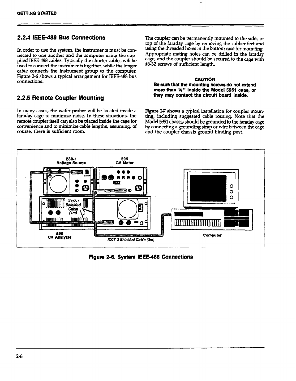
2.2.4 IEEE-488 Bus Connections
In order to use the system, the instruments must be connected to one another and the computer using the supplied IEEE-488 cables. Typically the shorter cables will be
used to connect the instruments together, while the longer
cable connects the instrument group to the computer.
Figure 2-6 shows a typical arrangement for IEEE-488 bus
coM&ions.
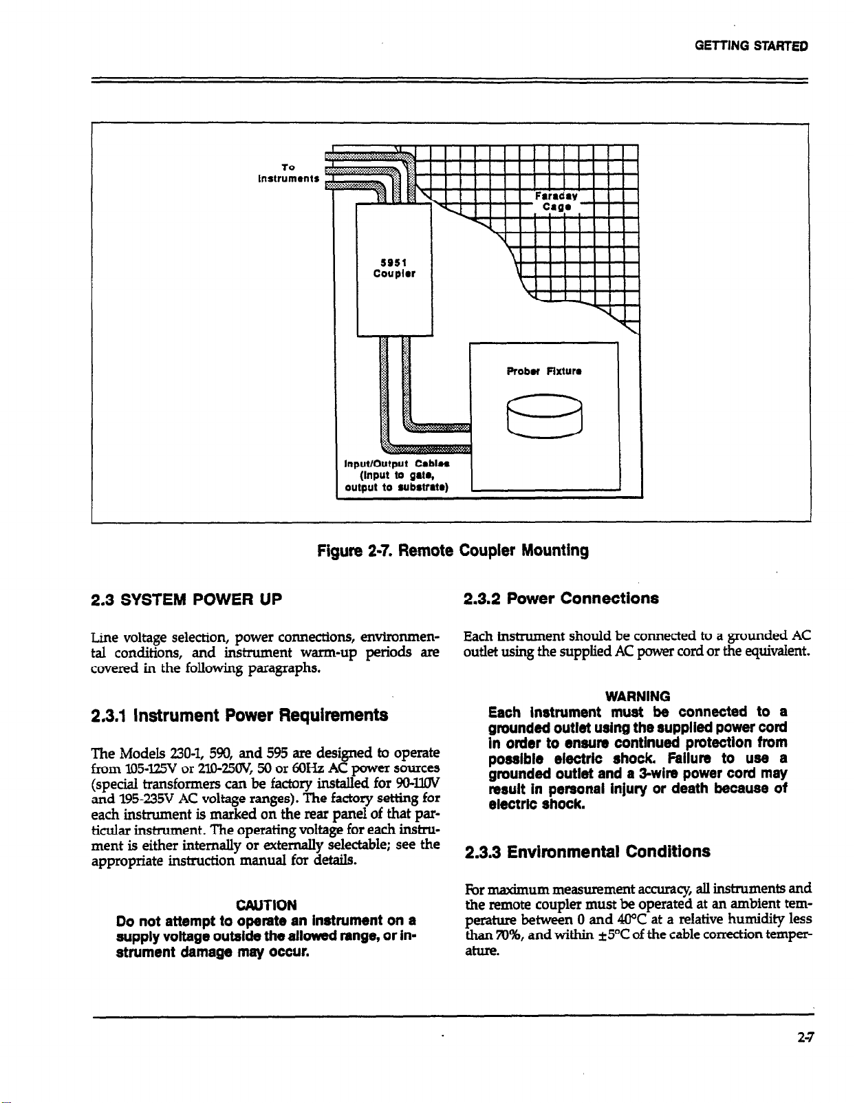
2.2.5 Remote Coupier Mounting
In many cases, the wafer prober will be located inside a
faraday cage to
remote coupler itself can also be placed inside the cage for
convenience and to minimize cable lengths, assuming, of
course, there is sufficient room.
nkimize noise. In these situations, the
230-l
Voltage !3ams
The coupler can be permanently mounted to the sides or
top of the faraday cage by removing the rubber feet and
using the threaded holes in the bottom case for mounting.
Appropriate mating holes can be drilled in the faraday
cage, and the coupler should be secured to the cage with
16-32 screws of sufficient length.
CAUTION
Be sum that the mounting scmws do not extend
more than Y4” inside the Model 5951 case, or
they may contact the circuit board inside.
Figure 2-7 shows a typical installation for coupler mounting, including suggested cable routing. Note that the
Model 5951 chassis should be grounded to the faraday cage
by connecting a grounding strap or wire between the cage
and the coupler chassis ground binding post.
2-4
7UU7-2 Shiekhi Ca#e pm)
Figure 2-6. System IEEE-468 Connections
Page 22
TO
Instruments
GETTING STARTEll
5951
Coupler
Probr Fixturm
Figure 2-7. Remote Coupler Mounting
2.3 SYSTEM POWER UP
Line voltage selection, power connections, environmental conditions, and instrument warm-up periods are
covered in the following paragraphs.
2.3.1 Instrument Power Requirements
The Models 2304, 590, and 595 are designed to operate
from 105425V or 2lO-250X 50 or 6OHz AC power sources
(special transformers can be factory installed for 904.W
and 195~235V AC voltage ranges). The factory setting for
each instrument is marked on the rear panel of that particular instrument. The operating voltage for each in&mment is either internally or externally selectable; see the
appropriate instruction manual for details.
CAUTION
Do not attempt to operate an instrument on a
supply voltage outside the aHowed range, or instrument damage may occur.
2.3.2 Power Connections
Each instrument should be connected to a grounded AC
outlet using the supplied AC power cord or the equivalent.
WARNING
Each instrument must be connected to a
grounded outlet using the supplied power cord
in order to ensure continued protection from
possible electric shock. Failure to use a
grounded outlet and a 3-wire power cord may
result in personal injury or death because of
electric shock.
2.3.3 Environmental Conditions
For maximum measurement accuracy, all instruments and
the remote coupler must be operated at an ambient tem-
perature between 0 and 4CPC at a relative humidity less
than 70%, and within *5T of the cable correction temperature.
2-7
Page 23
GElTING STARTED
2.3.4 Warm Up Period
.
The system can be used immediately when all instruments
are first turned on; however, to achieve rated system accuracy, all instruments should be turned on and allowed
to warm up for at least two hours before use.
2.3.5 Power Up Procedure
Follow the general procedure below to power up the
Package 82 system.
1. Connect the instruments together as outlined in paragraph 2.2.3.
2. Co~ect the instruments to the IEEE-488 bus of the host
?;4puter following the procedure given in paragraph
. . .
3. Turn on the computer and boot up its operating system
in the usual manner. Refer to the computer documentation for complete details for your particular system.
4. Turn on each instrument by pressing in on its liont
panel power switch. Verify that each instrument goes
through its normal power up routine, as described
below.
Model 230-l
1. The instrument first turns on all LEDs ind segments.
2. The software revision level is then displayed as in this
example:
Bl3
3. The unit then displays the primary address:
2. Thh,““‘” then displays the programmed primary
:
IEEE ADDRESS l.5
Verify the address is 15; program it for that value if not.
3. Finally, the unit begins displaying normal readings.
Model 595
1. The instrument first displays the ROM self-test message:
to.
2. The unit then displays normal readings.
3. Press MENU and verify the primary address is 23; set
it to that value if not.
2.3.6 Line Frequency
The Models 230-l and 590 can be operated from either 50
or 6OHz power sources with no further adjustments.
However, for the Model 595 to meet its stated noise
specifications, the unit must be programmed for the line
frequency being used. To set or check the Model 595 line
frequency, proceed as follows:
1. Turn off the Model 595 if it is presently turned on.
2. Press and hold the MENU button and then turn on the
power. Release the MENU button after the display
blanks on power up.
3. Press the MENU button and note .that the frequency
selection prompt is displayed:
IEl.3
4. The unit begins normal display.
Model 590
1. The Model 590 first displays the software revision level
as in this example:
590REVDl3
2-B
Fr - 50
or,
Fr = 60
4. Use one of the ADJUST keys to toggle the unit to the
desired frequency.
5. Press SHIFT EXIT to return to normal operation. Note
that the frequency selection prompt will remain in the
menu until power is removed.
Page 24

GETTING STARTED
2.4 SOFTWARE CONFIGURATION
The folIowing paragraphs discuss booting up the computer, making backup copies of the Package 82 software,
and loading and initializing the software.
2.4.1 Computer Boot Up
Before you can use the Package 82 software, the computer
must be booted up with the proper operating system software. See paragraph 1.9 for further information on computer requirements.
Turn on the computer and boot up BASIC 4.0 (if the com-
puter has ROM-based BASIC, no initialization is
necessary).
2.4.2 Software Backup
Before using the software, it is strongly recommended that
you make a working copy of the software supplied with
the Package 82. Since the software is not copy protected,
you can use the standard copy commands to duplicate
each diskette. After duplication, put the master diskette
away in a safe place and use only the working copy.
you intend to use. A typical example is:
MASS STORAGE IS “:,700,0“
Place the Package 82 software working disk in the
3.
default drive.
4.
Type in LOAD”PKG82CV” and press the EXEC key.
5.
After the program loads, press the RUN key, or type
in RUN and then press the EXEC key The main menu
shown in Figure 2-8 should appear on the computer
display.
2.4.4 Software Files
Package 82 software files that are included with the
distribution diskette are SulTLznarized in ‘Iable 2-2. Note that
“pkg82cal” is created when cable correction is performed
the first time.
2.5 SOFTWARE OVERVIEW
The main sections of the Package 82 software are discussed
in the following paragraphs. These decriptions follow the
order of the main menu shown in Figure 2-8. For detailed
information on using the software to make measurements
and analyze data, refer to Sections 3 and 4.
Use the COPY command to copy the software diskette.
A typical example is:
COPY “:I-lP9895,700,0” ‘IO “:HP9895,7OO,l”
Here, HP9895 represents the type of disk drive, 700 is the
primary address, and 0
Note that the working diskette should be formatted with
the INITIALIZE command before attempting copying.
and 1 are the disk drive numbers.
2.4.3 Software hitialization
Software initiakation is simply a matter of loading and
running a program as you would any other BASIC program, as outlined below.
1. Boot up or enter BASIC 4.0 in the usual manner.
2. If necessary, assign a mass storage specifier to the drive
2.5.1 System Reset
By selecting option I on the main menu, you can easily
reset the instruments and the software to default conditions. DCL (Device Clear) and IFC (Interface Clear) commands are sent over the bus to return the instruments to
their power-on states and remove any talkers or listeners
from the bus.
2.52 System Characterization
Option 2 on the main menu allows you to perform a
“probes up” characterization of the complete system from
the measuring instruments, through the connecting cables
and remote couple& down to the prober level:Characterization is necessary to null out (G, C#, or G), or remedy
leakage
sent in the system that could affect measurement accuracy;
the procedure also allows you to verify connection
problems.
currents, resistances, and stray capacitance pre-
2-9
Page 25

GETTING STARTED
f
l * PfICKflGE 82 MAIN MENU **
1. Reset Package 82 CU System
2. Test and Correct for System Leakages and Strays
3. Correct for Cabling Effects
4. Find Dtv~ct Cox and Equilibrium Delay Time
5. Make CV Measurements
6. halyze CU Data
7. Return to BASIC
Enter number to select from menu
Figure.24. Main Menu
There are two important aspects to systemcharackrktion:
1, Quasistatic capacitance (0, high-frequency capacitance
(C,), conductance (G), and Q/t (current) are measured
at a specified bias voltage to determine system contribution of these factors. Ce, CM, and G can be suppressed
in order to maximize accuracy. If abnormally large error terms are noted, the system should be checked for
poor connections or other factors that could lead to large
erms.
2. Q/t vs. V sweeps can be performed to determine the
presence of leakage resistance and extemal le
rent sources. C vs. V sweeps can be done to test
cur-
r the
7
presence of voltage dependent capacitance in the
system.
System checkout should be performed whenever the configuration, step V, or delay time is changed. Probes-up sup
pression should precede every measurement to achiwe
rated accuracy.
2.5.3 Cable Correction
Cable correction can be performed by selecting option 3
on the main menu. Cable correction is necessary to compensate for transmission line effects of the connecting
cables and is essential for maintaining accuracy of highfrequency CV measurements. In order to cable correct the
system, you must connect the Model 5909 Calibration
Sources to the system. Refer to paragraph 3.5 Correcting
for Cabling Rffects.
Included in the cable correction procedure is a gain correction of the Model 595 CV Meter. Cable correction and
gain unmction parameters are automatically stored on disk
during cable correction and are restored when the softwam
is run ini- so that correction need not be performed
each time the system is used. Note, however, that correction should be performed whenever the ambient temperature changes by more than 5OC, or if the system configuration is changed.
240
Page 26
GETTING STARTED
MOTE
The diskette for storing cable correction parameters
must be in the default drive when correction is
performed.
2.5.4 C, and Delay Time Determination
Option 4 allows you to determine optimum parameters for
measuring the device under test. The key areas of this
characterization process are:
1. A CV sweep of the device is used to find accumulation
and inversion voltages.
2. The device is biased in the accumulation region in order
to determine 6x.
3. The device is biased in inversion to determine Model
595 step time. A test for equilibrium can be performed
by monitoring the decay tune of Q/t to the system
leakage level following a step in DC bias voltage. The
user can also control a light on the device to help achieve
equilibrium.
4. A sweep of C and Q/t vs time delay is performed to
determine optimum delay time.
2.5.5 Device Measu@ment
Option 5 on the main menu allows you to perform a
simultaneous CV sweep on the device under test. As
parameters are measured, the data am stored within an
array for plotting or additional analysis, as required.
The two types of sweeps that can be performed include:
1. Accumulation to inversion: Initially, the device is biased
in accumulation, and the bias voltage is held static until Q/t reaches the system leakage level. The sweep is
then performed and the data are stored in the array.
2. inversion to accumulation: In this case, the device is first
biased in inversion, and the sweep is paused until
equilibrium is reached (when Q/t equals the system
leakage levei) . A submenu option allows you to control
a light within the test fixture (using the Model 5951
digital II0 port) as an aid in attaining the equilibrium
point. The sweep is then completed and the data are
stored in an array for further analysis.
the CRT or plotter, graphical analysis, and loading or storing array data on disk. Note that this option can also be
directly selected from menus providing sweep
measurements without having to go through the main
menu.
2.6 SYSTEM CHECKOUT
Use the basic procedure below to check out the Package
82 to determine if the system is operational. The procedure
requires the use of the Model 5909 Calibration Sources,
which are supplied with the package. Note that this pro-
cedure is not intended as an accuracy check, but is in-
cluded to show that all instruments and the system are
functioning normally.
2.6.1 Checkout Procedure
1. Connect the system together, as discussed in paragraph
2.2.
2. Power up the system using the procedure given in
paragraph 2.3.
3. Boot up the computer and load the Package 82 software,
as covered in paragraph 2.4.
4. Select option 2 on the main menu, and then option 2
on the &bsequent menu. Connect the l&F capacitor
and verify that C, is within 1% of the lkHz capacitor
value, and that Q/t is <IpA. Correct any cabling problems before proceeding.
Select the cable correction option on the main menu.
Ebllow the prompts and connect the Model 5909 Calibra-
tion Sources to the Model 5951 INPUT and OUTPUT
cables using the BNC adapters supplied with the Model
5909.
After correction, return to main menu selection 2, then
select option 2 on the submenu. Connect the 1.8nF
capacitor; verify that C, is within 1% of the lkH2
capacitance, and that CB is within 1% of the ICiXHz or
IMHz value (depending on the selected frequency).
Select option 3 on, the leakage and strays menu.
Turn on the sweep and observe the Model 590 voitage
display. Verify that the bias voltage readings step
thmugh the range of -2V to +2V in XhnV increments.
2.6.2 System lkoubleshooting
2.5.6 Data Analysis and Plotting
Option 6 on the main menu provides a window to a
number of analysis and graphing tools. Key options here
include printing out parameters, graphing array data on
Troubleshoot any system problems using the basic procedure shown in Table 2-3. For information on
troubleshooting individual instruments, refer to the respective instruction manual(s).
2-11
Page 27
GE-KING STARTED
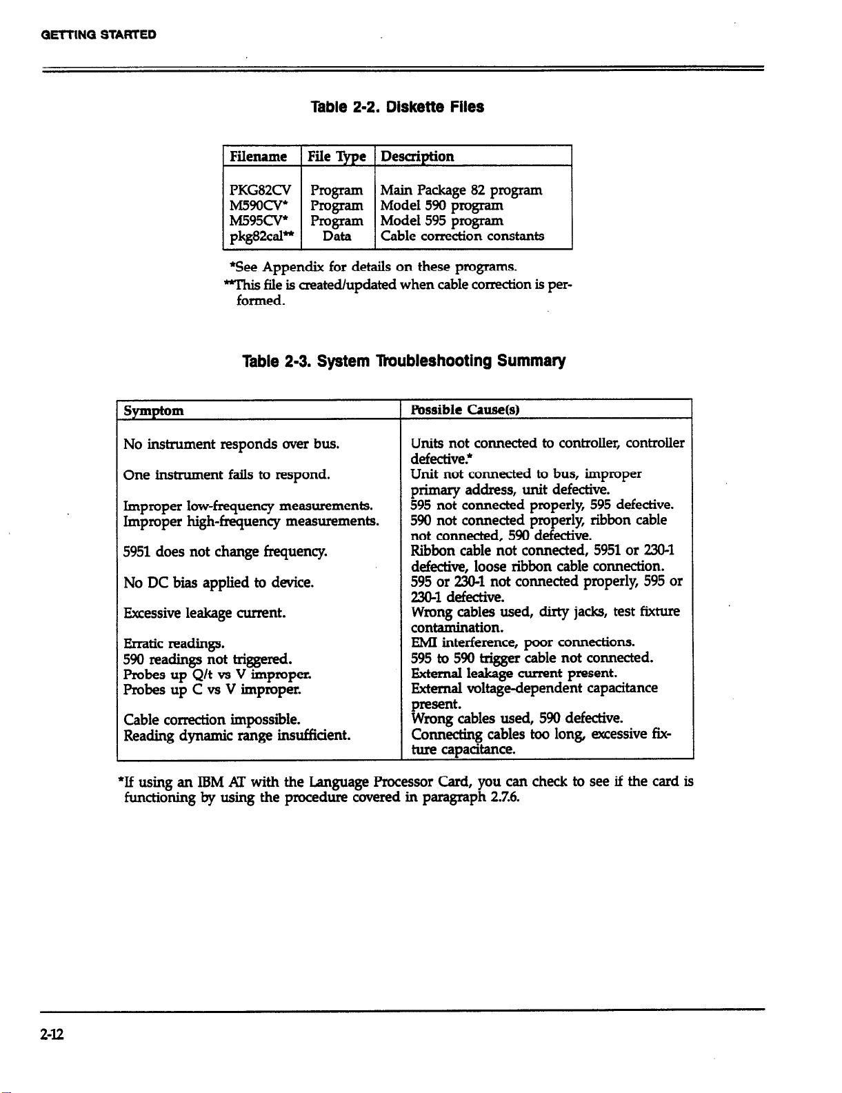
Table 2-2. Diskette Files
Filename File %e Description
PKG82CV Program
M5!3ocv* Program Model 590 program
M595cv*
P~.D~T Model 595 program
pkg82cal*
*See Appendix for details on these programs.
“this file is created/updated when cable correction is per-
formed.
Table 2-3. System liwbleshooting Summary
Symptom
No instrument responds over bus.
One instrument fails to respond.
Improper low-frequency measurements.
Improper high-frequency measurements.
5951 does not change frequency.
No DC bias applied to device.
Excessive leakage current.
Rrratic readings.
590 readings not triggered.
Probes up Q/t vs V improper.
Probes up c -3s v improper.
Main Package 82 program
Cable correction constants
Possible Cause(s)
Units not connected to controller, controller
defective.’
Unit not connected to bus, improper
primary address, unit defective.
595 not connected properly, 595 defective.
590 not connected properly ribbon cable
not cormected, 590 defective.
Ribbon cable not connected, 5951 or 230-l
defective, loose ribbon cable connection.
595 or 230-l not connected properly, 595 or
2304 defective.
Wrong cables used, dirty jacks, test fixture
contamination.
EMI interference, poor connections.
595 to 590 trigger cable not connected.
External leakage current present.
Eternal voltage-dependent capacitance
2-12
Cable correction impossible.
Reading dynamic range insufficient.
Ezt&bles used, 590 defective.
Connecting cables too long, excessive fixture capacitance.
*If using an IBM AT with the Language Processor Card, you can check to see if the card is
functioning by using the procedure covered in paragraph 2.7.6.
Page 28
GETTING STARTED
2.7 USlNG THE PACKAGE 82 WITH THE
IBM AT
The Package 82 can be used with IBM AT computers (and
some compatibles such as the HP Vectra) that are equipped with the HP 8232lA Language Processor Card. The
HP BASIC 5.0 ROM must be installed on the processor card
in order to support the Package 82 software. Note that an
EGA monitor is recommended (a monochrome monitor
will work, but displayed graphs will be somewhat small).
The following paragraphs give a brief overview of hardware and software installation, configuration file, and
methods to change the print path to support a parallel or
serial printer. Refer to the documentation supplied with
the processor card, BASIC ROM, and programming
language for detailed information.
2.7.1 Installation
IbIlow the overall procedure below to install the hardware
and software.
1.
Install the HP BASIC ROM on the processor card, as
discussed in the HP BASIC ROM Installation Instructions. Be sure to place the ROM jumper in the RUM
IN position.
2.
Install the processor card in the IBM Al’ computer, as
discussed in the Language Processor Instructions.
3.
Connect the IEEE-488 bus of the Package 82 instruments
to the I-IPlB connector of the processor card. See paragraph 2.2.4 of this instruction manual for more information on IEEE-488 bus connections.
4.
Boot up the IBM AT computer with MS-DOS.
5.
Install the BASIC Language software, as discussed in
the HP BASIC ROM Installation hstructions.
2.7.3 Configuration File Modification
The configuration file, HPW.CON, must be modified to
redefine the display mode1 type to combined alphal
graphics for use with the Package 82. To do so, run the
CONFXXE utility from MS-DOS, and change the machine
type to “9816 combined”, Save the new configuration before
exiting the CONEEXE utility. Remember that the
I-IPW.CON file must be in the directory of the disk you
use to BOOT the system.
2.7.4 Booting the System
Use the appropriate procedure below to boot BASIC and
load the Package 82 software. These procedures assume
that you have followed the software installation instruc-
tions given in the HP BASIC ROM Installation Instructions.
Hard Disk System Boot-up
The procedure below assumes that drive C is your hard
disk, and that you have created a directory called HPW
as part of the installation procedure. All pertinent HP files
must exist under the HPW directory.
1.
Type the following:
C: <Enter>
CD \HPW <Enter>
2.
If you have.not already done do, copy the Package 82
soflwanzintotheI-IPWdirectorybyusingtheHPWUTIL
utility program supplied with HP BASIC. Select the LIP
to HPW option for copying for master disks, or use
HPW to I-IPW copy for working disks copied with
HPUTIL utility.
3.
After the disk has been copied, boot the system by typing the following:
2.7.2 Software Backup
Before using the Package 82 software, it is strongly recommended that you make working copies of the supplied
disks, and use only the working disks on a day-to-day
basis. To do so, perform an LIFto-HPW copy using the
HPWUTIL utility supplied with the HP BASIC package.
Note that disks copied to the HPW format can only be used
on MS-DOS drives along with the HP BASIC system; these
copies cannot be used on HP Series 200 or 300 drives.
BOOT e Enter >
4.
After the boot-up sequence has finished, type the
following to enter BASIC:
HPBASIC <Enter >
5.
Load the Package 82 software as follows:
LOAD ‘TKG82CV” <Enter >
(Or use ‘M59OCV or ‘M595CV filenames for those
Programs).
2-13
Page 29

GE-KING STARTED
6. RUN the program in the usual manner. Refer to the remainder of Section 2, as well as Sections 3 and 4 for
detailed operation information.
Flexible Disk System Boot-up
1. Place the HP BASIC working disk into the default drive,
and type the following:
BOOT <Enter >
2. After the boot-up procedure, enter the following:
HPBASIC <Enter >
3. Place the Package 82 working disk in the default drive,
and type the following:
LOAD “PKG82CV” <Enter>
(Or use “M59OCV” or “M595CV” filenames for those
Programs.)
4. RUN the
3, and 4 or detailed operation information.
rogram in the usual manner. See Sections 2,
4
2.7.5 Modifying the Print Path
As supplied, the Package 82 software supports a printer
connected to the HP-IB bus with a primary address of 1.
The program must be modified to support printers con-
nected to the parallel or serial ports of the IBM AT’ as
outlined below. Note that such printers must emulate HP
Think Jet bit-mapped graphics in order to properly display
graphs generated by the Package 82.
1. Boot up HP BASIC and the ‘PKG82CV” (or “M59OCV’
or “M595CV”) programs, as described above.
2.Type the following in order to locate the Printpath
variable in the program:
Printpath = 26
For the serial port (COMl), modify the Printpath as
follows:
Printpath = 9
(Note: It may also be necessary to modify the configuration file for oroner serial sort oneration. See the HP
BASIC La&rag; Programmer’s Reference Guide.)
Save the modified program under a convenient name.
4.
Use the modified program in order to support the
parallel or serial printers.
2.7.6 Operational Check
After software and hardware installation, the procedure
below can be used to determine if the language processor
card is properly communicating with the instruments.
1. Connect the instruments to the IEEE-488 connector on
the back of the IBM AT computer.
2. Turn on the computer, boot MS-DOS, then boot up HP
BASIC, as described in paragraph 2.7.4.
3. Turn on the instruments; make sure they go through
their normal power-up cycles, and that the primary addresses of the instruments are set to their default values
(2304 X3; 590, W; 595,28). If not, set or program the primary address to the correct value(s).
4. .From the HP BASIC direct mode, type in the following
command, and verify that the Model 230-1 displays XJVz
OUTPUT 7X3 ; ‘VIOXfl <Enter>
5. Type in the following, and note that the Model 590 goes
into the autorange mode:
OUTPUT 7.5; ‘W <Enter>
6. Type in the following, and verify that the Model 595
changes to the current function:
FIND ‘l%ntpatW <Enter>
3. When the computer displays the line in which Printpath
is defined, modify the variable as follows (for the parallel
Dolt. ml:
L .
I
2-14
OUTPUT 728 ; ‘TW <Enter>
Page 30
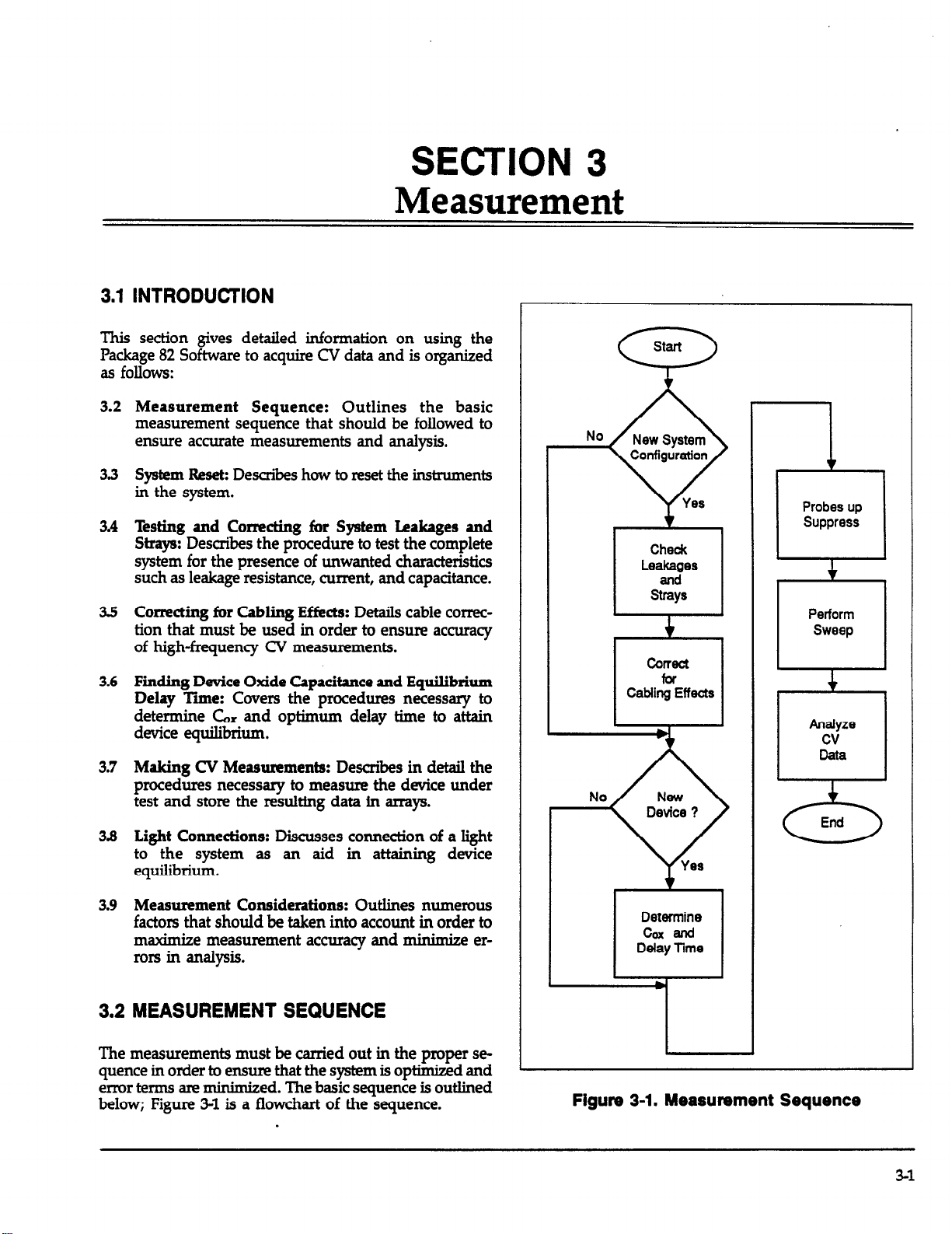
SECTION 3
s
Measurement
3.1 INTRODUCTION
This section gives detailed information on using the
Package 82 Software to acquire CV data and is organized
as follows:
3.2
Measurement Sequence: Outlines the basic
measurement sequence that should be followed to
ensure accurate measurements and analysis.
33
System Reseh Describes how to reset the instruments
in the system.
3.4
Testing and Correcting for System Leakages and
Strays: Describes the procedure to test the complete
system for the presence of unwanted characteristics
such as leakage resistance, current, and capacitance.
35
Correcting for Cabling Pffecta: Details cable correction that must be used in order to ensure accuracy
of high-frequency CV measurements.
3.6
Finding Device Oxide Capacitance and Equilibrium
Delay The: Covers the procedures necessary to
determine Cax and optimum delay time to attain
device equilibrium.
3.7
Making CV Measurements: Describes in detail the
procedures necessary to measure the device under
test and store the resulting data in arrays.
38
Light Connections: Discusses connection of a light
to the system as an aid in attaining device
equilibrium.
3.9
Measurement Considerations: Outlines numerous
factors that should be taken into account in order to
maximize measurement accuracy and minimke er-
rors in analysis.
The measurements must be carried out in the proper sequence in order to ensure that the system is optimized and
ermrtermsare minimized. The basic sequence is outlined
below; Figure 3-l is a flowchart of the sequence.
0
No
rv
Figure 3-1. Measurement Sequence
N6W
Device ?
Yes
Perform
Sweep
Analyze
cv
Data
End
3-l
Page 31

MEASUREMENT
Step 1: Test and Correct for System Leakage and Strays
Initially, you should test your system to determine if any
problems such as excess leakage current or unwanted
capacitance are present. You should correct any problems
before continuing. Note that the system need be tested only when you change some aspect of its configuration (such
as connecting cables or test fixture).
Suppression, which is also available under this menu op
tion, should be performed before each measurement for
optimum accuracy. Note that suppression can also be performed from a measurement menu by pressing ‘7’.
Step 2: Correct for Cabling Effects
Cable correction is necessary to compensate for transmission line effects through the connecting cables and remote
input coupler Failure to perform cable correction will result
in substantially reduced accuracy of high-frequency CV
measurements. In order to perform correction, it will be
necessary for you to co~ect the Model 5909 calibration
capacitors. Cable correction need be performed only if the
system configuration is changed in some manner, or if the
ambient temperature changes by more than 5°C.
Step 3: Determine Oxide Capacitance and Equilibrium
Delay Tiie
The device must be tested to determine optimum delay
time to maintain equilibrium as well as to determine 6x.
Cax is determined with the device biased in accumulation.
The device can then be biased in inversion to determine
optimum delay time for equilibrium by plotting C and Q/t
versus delay time. Note that these parameters must be
determined for each device.
Step 4: Make CV Measurements
Now that all the “housekeeping, so to speak, is out of the
way, a sweep can be performed to determine how such
device parameters as capacitance change with applied DC
bias voltage. First, of course, it will be necessary for you
to select such parameters as range, frequency, and bias
voltage values. As the sweep ia performed, measured
values are stored in arrays for later retrieval and analysis.
Step 5: Analyze CV Data
Once a sweep has been performed and the results am
stored safely in computer arrays, you can apply any one
of a number of different analysis techniques to the data.
Raw data plotting (hard copy) or graphing (CRT) of such
parameters as low and high frequency capacitance vs. V
can be performed. Analysis features including doping profile, flatband calculations, and interface trap density are
also provided. See Section 4 for analysis.
3.3 SYSTEM RESET
Option 1 on the main menu (Fiie 3-2) allows you to reset
your Package 82 System and return the instruments to their
default conditions. When this option is executed, the
IEEE-488 IFC (Interface Clear) and SDC (Selective Device
Clear) commands are sent over the bus, and you will then
be returned to the main menu after a two-second pause.
During this period, the computer will display the following message:
Outputing IFC and SDC to reset system.
The IFC command removes any talkers and listeners from
the bus, and the SDC comman d returns instruments to
their default conditions. The Models 230-l and 595 will
always return the the same default state, but the default
conditions for the Model 590 are determined by SAVE 0.
See the appropriate instruction manuals for details. Note
that the instruments are automatically reset when the program is first run, and that only the Models 230~1,590, and
595willbeaffeckdbytheSDCComman d; the disk drive,
printer; or other peripherals will not be affected.
3-2
Page 32

MEASUREMENT
f
l * PWKACE 82 MAIN MENU **
1. Reset Package 82 CU System
2. Test and Correct for System Leakages and Strays
3. Correct for Cabling Effects
4. Find Device Cox and Equilrbrlum Delay Time
5. Make CU Measurements
6. halyze CU Data
7. Return to BASIC
Enter number to select from menu
L
T
J
Figure 3-2. Package 82 Main Menu
3.4 TESTING AND CORRECTING FOR SYSTEM
LEAKAGES AND STRAYS
The system should be tested with the probes up to determine if any sources of large mrs such as defective cables
are present. The following paragraphs give an overview
of the process, discuss menus, and detail the procedure
for testing your particular system,
Suppression should be performed prior to each measurement for optimum accuracy.
3.4.1 Test and Correction Menu
‘EY test your system, select main menu option 2, Test and
Correct for System Leakages and Strays.
Figure 3-3 shows the overall test and correction menu for
the Package 82 software. Thnwgh this menu, you can
select measurement parameters, monitor leakage levels,
perform a probes-up sweep, analyze the results, and suppress offsets. These aspects are covered in the following
paragraphs*
3-3
Page 33

MEASUREMENT
f
** Measure stray capacitance and leakage currents *+
Open the circuit at the device (ie. probe up).
Suppress should be done before each device measurement,
1. Set Measurement Parameters
2. Monitor/Suppress System Strays and Leakages
3. Measure Leakages Over Sweep Voltage Range
4. Analyze Sweep Data for C and Q/t vs. V
5. Return to Main Menu
Enter number to select from menu
Figun, 3-3. Stray Capacitance and Leakage Cunent
3.4.2 Parameter Selection
Menu Selections
By selecting option 1 on the system testing menu, you can
access the parameter selection menu shown in Fii 3-4.
YXI can also access this menu by pressing ‘W from
measurement menus. This menu allows you to program
the following parameters:
1. Range for both quasistatic and high-frequency measurements (2ClIpF or 2nF). The measurement ranges of both
the Models 590 and 595 are set by this parameter.
2. Frequency for high-frequency measurements (lOOkHz
or MHz). This parameter sets the operating frequen-
cy of the Models 590 and 5951.
3. Model (parallel or series). Model selects whether the
device is modeled as a parallel capacitance and conductance, or a series capacitance and resistance.
Q.StartV:(-120sVsl2O).StartVistheinitialbias
voltage setting of a CV sweep.
S.StopV:(-l20sVsl2O).StopVisthefinalbias
voltage setting of a CV sweep.
6. Bias V: Bias V is a static DC level used when static
monitoring the system (for example, when testing for
leakages and strays), and is the voltage level assumed
when a sweep is completed.
7. T delay: (0.07 s T s 199.99~~). Note that the time
delay must be properly set to attain device equilibrium.
3-4
Page 34

MEASUREMENT
8. Step V: (lOm%‘, 2OrriV, SOmV, or lOOmV): Step V is the
incremental change of voltage of the bias staircase
waveform sweep.
9. C-Cap: (Corrected capacitance). Uses the corrected
capacitance program of the Model 595 when enabled.
l * measurement parameter list l *
Range :
Freq : 2
Model :
start v:
stop v:
Bids V:
T-delay:
Step V:
C-cap :
Filter: 2
I Enter Rl for 200pF, RZ for ZnF
Enter Fl for 100KHZ, F2 for 1MHZ
I
-5.00 il. Enter An,
5.00 v. Enter On,
0.00 v. Enter Bn,
.07 sec. Enter Tn, 0.07 i= n <= 199.99
50 mV.
1
Enter Ml for parallel, M2 for series
-120 <= n <= 120
-120 <= n <- 120
-120 <= n <- 120
Enter S10, S20, S50 or S1OO
Enter Cl for correction oft, C2 for on
Enter II for filter off, I2 for on
C-Cap should be used only when testing leaky devices.
10. Filter: Sets the Model 595 to Filter 2 when on, Filter
0 (off) when off.
NOTE: Turning off the filter will increase the noise by
2.5 times.
Number of samples = 94
NOTE : 1) Keep start V and stop V within 40 volts of each other.
2) Keep number of samples within 4 and 1000 points with filter off.
3) Keep number of samples within 50 and 1000 points wrth filter on.
enter changes one change at a time. enter E when done, l for files
Figure 34. Parameter Selection Menu
3-5
Page 35

MEASUREMENT
Programming Parameters
To program a parameter, type in the indicated menu letter followed by the pertinent parameter. The examples
below wilI help to demonstrate this process.
Example 1: Select IMHz I-&h-frequency Operation
To select high frequency operation, simply type in F2 at
the command prompt and press the ENTER key.
Example 2: Program a +lSV Bias V
Type in Bl5 and press the ENTER key.
Example 3: Select O.&x Delay Time
‘Qpe in To.1 and press the ENTER key.
Example 4: Program a 20mV Step Voltage
Type in S20 and press the ENTER key.
3. Bias voltage polarity is specified at the gate with respect
to the substrate. For example, with a positive voltage,
the gate will be biased positive relative to the substrate.
Thus, an n-type material must be biased positive to be
in the accumulation region.
NOTE
The voltage displayed on the front panel of the
Model 590 is of the opposite polaritv from the
voltage displayed by %e Package 82 software
because of the gate-to-substrate voltage convention
used. As described in Section 2, INPUT should
be connected to the gate terminal, and OUTPUT
should be connected to the substrate terminal.
Savin@Recailing Parameters
By pressing the N * m
key, you can save or load parameters
to or from diskette. The menu for these operations is
shown in Figure 3-5. Press ‘9 (save) or “I? (load) to carry
out the desired operation. You will then be prompted to
type in the filename to be saved or loaded. An error
message will be given if a file cannot be found or will be
overwritten.
Programming Considerations
When sekxting parameters, there are a few pointsto keep
in mind, including:
1. The maximum difference between the programmed
Start V and Stop V is 4CiV Exceeding this value will
generate an error message.
2. Thenumberofpointsmustbebetween4andXXHIwith
the filter off, and between 50 and lOO0 with the filter
on to avoid curve distortion.
When the save option is selected, the parameter values currently in effect will be saved under the selected filename.
Parameters loaded from an existing file will overwrite ex-
isting parameters.
Rehrning to Previous Menu
After all parameters have been programmed (or loaded
from disk), pss “E” to return to the system leakage testing
menu.
3-6
Page 36

l * Store / Load system parameters **
loading parameters overwrites the system parameters.
A filt must already exist to be Loaded.
A flie to be Stored must not exist.
MEASUREMENT
enter S or L to store or load parameters, enter E to exit
Figure 36. Save/Load Parameter Menu
Page 37

.
3.4.3 Viewing Leakage Levels
Description
Before performing a test sweep, you should observe system
leakage current and capacitance and fix any problems
before continuing. Once system leakage levels have been
reduced, proceed to paragraph 3.4.4 to perform a probesup sweep of the system. Paragraph 3.9 discusses these factors in more detail.
Procedure
1. Select option 2 on the main menu followed by option
1 on the following menu. Program the following:
Range: 200pF
Frequency: 1OOkHz or lMHz as required
Model: Parallel
Bias V: O.OOV
T Delay: 0.07sec
Step V: 5OniV
C-cap: Off
Filter: On
Press 7’ then ENTER when parameters have been pro-
grammed, then select option 2, Monitor/Suppress
System Strays and Leakages.
2. Disconnect the device from the system; in other words,
place the probes in the up position. Close the shield
on the test fixture.
3. If necessary, press ‘X” to turn off suppress and display
“rati readings.
4. You will then see a display similar to the one shown in
Figure 3-6. The values shown are representative of what
to expect in a typical system, but your values may be
somewhat different.
5. Note the quasistatic and high-frequency capacitance and
the leakage (Q/t) level. These values should be as small
as possible. Ideally stray capacitance should be less than
1% of the capacitance you expect to measure for OP-
timum am&y. Also, l&age *&-rent should be as I&
as possible.
6. If desired, press 2” to suppress &, C, and G.
Analyzing the Results
There are two key items to note when performing the
above procedure: (1) excessive leakage current (Q/t), and
(2) too much stray capacitance. If excessive leakage cur-
rent is noted, you should check the following:
1. Make sure the proper cables are installed in the correct
places. Be certain you have not interchanged Model 4801
(low-noise) cables with the Model 7051 @On) cables.
2. Make sure all connecting jacks and connectors are free
of contamination. Clean any dirty connectors with
methanol and allow them to dry thoroughly before use.
3. Be certain that you are, in fact making a “probes-up
measurement.
4. Check to see that no leakage paths are present in the
test fixture.
5. If necessary, tie down cables to avoid noise currents
caused by cable flexing. Also, avoid vibration during
testing.
Things to check for excessive stray capacitance include:
1. Verify that all cables are of the proper type and not of
exessive length.
2. Vxify the integrity of all cable shields and that the shield
co~ections are carried through to the connectors.
3. Again, make sure the procedure is being performed in
the “probes-up” configuration.
4. Use a test fixture of good, low-capacitance design.
5. Make certain the test fixture shield is in place when
characterizing the system. The same precaution holds
true when characterizmg or measuring a device.
3-8
Page 38

++* monitor/suppress system strays and leakages at Bias V ++*
Open the circuit at the device (it. probe up).
Press ‘II’ to set measurement parameters.
Press ‘Z’ to suppress Cq , Ch, and G (probe ucj, suppress on ).
Press ‘R’ to monitor raw Cq, Ch, and G (probe up, suppress off).
Press ‘Q’ to Quit.
(note: Keyboard response time is affected by delay time)
Suppress is ON.
MEASUREMENT
Quasistatic : Cq (pF) p/t (PA)
48.65 -.060
High freq :
.
Ch (pF)
48.78 6.0000E-01
Figure 3-$. Monitor Leakage Menu
3.4.4 System Leakage Test Sweep
Description
This aspect of system leakage testing allows you to deter-
mine if there are any voltage-dependent leakages in the
system. Basically there are two important points here: (1)
how the leakage current varies as the bias voltage changes,
and (2) apparent quasistatic capacitance variation with
changes in voltage. These considerations are discussed
more completely in paragraph 3.9.
G (US) Bias Vgs I
* 060
/
Procedure
1.
Select option 2 on the main menu, then option 1, set
measurement parameters, and program the following
parameters.
Range: 2OOpF
Frequency: 1ookHz or l.MHz, as required
Model: Parallel
Start V Most negative voltage generally used.
Stop V: Most positive voltage usually used.
3-9
Page 39

MEASUREMENT
Bias v: 0.W
T delay: 0.07~~
Step V: lOOmV
C-Cap: Off
Press “E” then ENTER to exit. Select option 3, Measure
Leakages over Sweep Voltage Range.
2. Place the DrObeS in the UD DOSitiOn t0 diSCOMeCt the
device from the system. L l
Make sure the test fixture shield is in place before star-
ting the procedure.
Press ‘W to dispiay “rad’ readings. The computer
display will show leakage levels, as shown in Figure 3Z
Press “S” to initiate the sweep. During the sweep, the
computer will display the following:
sweep in progress.
Also, the sweep duration will be displayed.
6.
At the end of the sweep, the PROBES UP DATA
ANALYSIS MENU will be displayed:
1. Graph both C, and C, vs. Gate Voltage.
2. Graph Q/t Current vs. Gate Voltage.
3. Graph Conductance vs. Gate Voltage.
4. Return to Previous Menu.
z
Select the desired sweep data option on the menu, to
graph both quasistatic and high-frequency capacitance
vs. gate voltage, and Q/t current vs. gate voltage.
Analyzing the Resdts
The leakage current you may observe during testing could
be from two main sources: (1) constant leakage currents
due to such sources as cables, and (2) voltage-dependent
leakage currents caused by leakage resistances. A typical
constant leakage current curve is shown in Fii 3-s,
while a Q/t curve due to leakage resistance is shown in
Figure 3-9. In the first case, note that the current is con-
stant and does not depend on the applied voltage. For the
case of curve dependent on leakage resistance, however,
the current is directly proportional to the voltage, as is the
case with any common resistor. The resistance, incidently,
is simply the reciprocal of the slope of the line.
Since quasistatic capacitance is determined by integrating
the current, the presence of unwanted leakage current will
skew your qua&static CV curves. Figure 3-10 shows the effects of constant leakage current. Here, the normal parasitic
capacitance, C r, is skewed upwards with an additional
“phantom” capacitance added to the normal parasitic
capacitance. The same type of curve skew will also occur
with normal measurements, but its effects will usually be
less no&able because of the larger capacitance levels
involved.
A more serious situation is present in the case of the varying current, as shown in Figure 3-11. Now, the usually flat
capacitance curve has been tilted, resulting in what is
essentially a voltage-dependent capacitance. Again, the
same curve-tilting effects can be expected for normal
measurements, although usually to a lesser degree.
The high-frequency capacitance curves will not generally
show any voltage-variability, and will show mainly
parasitic capacitance at the frequency of interest. Such
curves can also provide a good frame of reference for the
quasistatic curves, as both quasistatic and high-frequency
curves should be flat and very simihu as long as leakage
currents are sufficiently low.
The G vs. V curve shows AC loss at the selected measurement frequency (lOOm or YMHz). The high frequency
conductance value may represent a leakage resistance that
is AC coupled into the test fixture.
Page 40

f
l * manual start sweep measurement l +
Open the circuit at the device (it. probe up).
Press ‘M’ to set measurement parameters.
Press ‘Z’ to suppress Cq, Ch, and G (probe up, suppress on).
Press ‘R’ to monitor raw Cq, Ch, and G (probe up, suppress off).
Press ‘S’ to start sweep.
Press ‘Q’ to Quit.
(note: Keyboard response time is affected by delay time)
Suppress LS ON.
Sweep wrll take .4 minutes.
MEASUREMENT
Quaslstat lc : C4 (pF)
57.19
High freq :
Ch (pF) G (US) Start Vgs
57.58
Figum 3-7. Diagnostic Sweep Menu
o/t (pi+)
- .,200
1.1000Et00 -4.950
Page 41

MEASUREMENT
C
---------- ----------- c wth
Leakage
---------- ----------- c Without
Leakage
1
V
Figure 3-8. Leakage Due to Constant Current
v
Figure 3-9. Wt Curve with Leakage Resistance
Figure 3-10. Constant Leakage Current increases
Quasistatic Capacitance
C
/
/
/
0
/
----------/
/
/
/
./
Figure 341. Quasistatic Capacitance with and
without Leakage Current
,
h ---------- c Without
/
/
.
.
/
/
/
,/ C With
/
Leakage
Leakage
V
342
Page 42

MEASUREMENT
3.4.5 Offset Suppression
Description
By selecting option 2 on the system leakage test menu, you
can monitor the parameters listed below at a fixed bias
voltage. This feature will give you an opportunity to suppress these leakage values to maximize accuracy. This sup
pression procedure should be carried out before each
verified or performed measurement for optimum accuracy.
NOTE
Large leakage currents and stray capacitances
should not be suppressed. Determine the source
of the problem and correct it before using your
system if large offsets are noted.
Monitored parameters include:
C, (quasistatic capacitance)
Q/t (leakage current)
CH (high frequency capacitance)
G (conductance)
VGs (gate voltage)
Suppressed parameters include Ce, CM, and G. Note that
Q/t is not suppressed. Note that suppress on/off can be
controlled from a measurement menu by pressing “z”
(suppress on) or ‘y (suppress off).
Disabling Suppress
To disable suppress and display raw readings, simply press
“R” at the command prompt.
3.5 CORRECTING FOR CABLING EFFECTS
Cable correction is necessary to optimize accuracy of high-
frequency CV measurements, and to align C, and CM for
D, measurements. The process involves connecting calibration capacitors with precisely-known values to the con-
necting cables in place of the test fixture. Once correction
is completed, correction constants are written to a disk file
called “pkg82ca.l” and are recalled when the program is
run.
The following paragraphs discuss required calibration
sources as well as the overall cable correction procedure.
3.51 When to Perform Cable Correction
Cable correction must be performed the first time you use
your system. Thereafter, for optimum accuracy, it is recommended that you cable correct your system whenever the
ambient temperature changes by more than 5°C from the
previous correction temperature. XXI can cable correct your
system daily, if desired, but doing so is not absolutely
essential.
Procedure
1. Disconnect the device from the system; in other words,
place the probes in the up position. Close the shield on
the probe fixture.
2. Select option 2, Monitor/Suppress System Strays and
Leakages. You will then see a display similar to the one
shown in Pii 3-6. The values shown here are
representative of what to expect in a typical system, but
yours could be somewhat different.
3. Press “Z” to suppress the leakage values. The Model 590
will be drift corrected, and its zero mode will be enabled
to suppress CH and G. Suppress on the Mode1 595 will
also be enabled to suppress C, after a E-second pause
t; szfznie status of suppress (on) will be displayed
.
4. Press “Q”’ to return to the previous menu once suppression is complete.
NOTE
Cable correction parameters are stored on diskette
in the “pkg82cal” file. These correction parametem
are automatically retrieved during program in-
itialization. The diskette containing correction
parameters is in the default drive when running
the program.
3.5.2 Recommended Sources
Table 3-l summarizes the recommended calibration
capacitors, which are part of the Model 5909 calibration
set supplied with the Package 82. The values shown are
nominal; you must use the IkHz, XUcHz, and lMHz
values marked on the sources when correcting your
system. Space has been provided in Table 3-l for you to
enter the actual values of your sources.
Page 43

MEASUREMENT
Table 3-l. Cable Correction Sources
Nominal
valus Value*
mokH2
V.uen
IMHZ
Value*
47pF - - 18OpF - - 47OpF _ - -
1.8nF - - -
*Nominal values inlcuded with Model 5909 Calibration
Source
“Enter values from sources where indicated.
5951
Remote Input Coupler
3.5.3 Source Connections
In order to correct your system, it will be necessary for you
to disconnect your test fixture and connect each calibration capacitor in its place when prompted to do so, as
shown in Figure 342. Use the supplied female-to-female
BNC adapters to connect the sources to the cables.
When using the sources, be sure not to handle them excessively, as the resulting temperature rise will change the
source values due to temperature coefficients. This
temperature change will degrade the accuracy of the correction process.
3-14
Figure 342. Cable Correction Connections
Page 44

MEASUREMENT
3.5.4 Software Modif ication
Before cable correcting your system the first time, it will be
necessary for you to modify the software with the actual
values of your particular calibration capacitors. This step
is necessary because each set of sources has slightly different capacitance values. The software need not be
modified again unti you re-characterize your sources.
In order to modify your software, proceed as follows:
1. Load the Package 82 software in the usuaI manner, but
do not RUN it.
2. LIST the first 30 to 40 lines of the program and locate
the I2 string variables that contain the source values,
as shown in Figure 3-13. The exact line numbers may
vary depending on the software revision level.
I
620
620
621
630
640
650
651
660
670
680
681
690
700
710
71i
720
730
740
! CALIBRATION SOURCE CONSTANTS
!
C547n$="4.7000E-11"
Cs47q$="4.7000E-11"
Cs47k$="4.7000E-1L"
Cs47m$="4.7000E-11"
Cs180n$="
Csl80q$='l.#000E-10"
Cs180k$="1.8000E-10"
CslSQm$=“l.8000E-10”
Cs470n$=“4,7000E-10”
Cs470q$=“4.7000E-10”
Cs470k$="4.7000E-10"
Cs470n$="4.7000E-10"
Cs1800n9-"1.8000E-9"
Cs1800q$-“1.8000E-9”
Cs1800k$="1.8000E-9"
Cs1800m$=“1.8000E-9”
1.3000E-10"
3. Enter the EDIT mode and modify the variables with the
actual UcHz, lOOkH.z, and MHz values marked on your
sources. In the string variables, “n” represents the
nominal value (which should not be changed unless you
are using different sources), “q” represents lk&, ‘Y
is lfRXHz, and “rri’ indicates MHz. Rx example, if your
1.&d? source has an actual 1OOkHz value of 1.802nF,
modify the code as follows:
680 csl8ook$=“1.802E-9”
NOTE
Nominal values can be changed, but the recommended source values are 25% (47,470) and 90%
(l80,BOO) of full scale.
! 47pf NOMINAL
! 47pF at 1KHz
! 47pF at 100KHz
! 47pF at IMHz
! 180pf NOMINAL
! 180pF at lKHz
! 180pF at 100KHz
! 180pF at 1MHz
! 470pf NOMINAL
! 470pF at lKHz
! 470pF at 100KHz
! 470pF at 1MHz
! 1800pf NOMINAL
! 1800pF at 1KHz
! 1800pF at 100KHz
! 1800pF at 1MHz
Figure 3-13. Partial Listing Showing Nominal Source Wues
345
Page 45

MEASUREMENT
4. After modifying all 12 variables, save the program as
a working file. Be sure that you use this modified program instead of the original from now on; otherwise,
the cable correction procedure will yield erroneous
calibration values, resulting in improper measurements.
3.55 Correction Procedure
As noted earlie& the following procedure must be performed the first time you use your system, and it should be
done when the ambient temperature changes by more
than 5°C from the previous correction point. Proceed as
follows:
1. Load the modified Package 82 software (see paragraph
3.5.4) and RUN it in the usual manner.
2. Select option 2 and monitor the leakage current to assure
proper hookup. Next, connect a calibration source to
verify hookup, and return to the main menu.
3. Select option 3, Correct for Cabling Effects, on the main
menu.
4. The ~romam will then enter the cable correction nortion if t&e program. Initially you will be prompted to
be sure that the calibration source values have been
altered as described above. The actual source values will
be displayed.
Disconnect the cables from the chuck when prompted
to do so, and press ENTER to continue.
FolIow the prompts to complete the correction process.
For each range and frequency, you wiIl be prompted
when to disco~ect the cables and connect the appropriate sources, as shown in Pii 3-U. After each
correction, you wilI be given an opportunity to retry
(press ‘WY. The Retry option will allow you to repeat
the correction for the presently-selected range and frequency (for example lIlOkHz/2nF or lMHz12OOpF).
NOTE
Be sure to connect the right sources as no error
messages will be given for improper correction.
When correction is completed, you wiIl be returned to
the main menu.
If you wish to verify correction accuracy select option
2 on the main menu (Testing for Leakages and Strays)
and then monitor system readings with calibration
sources connected. Be sure to select the appropriate
range and frequency for the sources being measured.
Note: If a mistake was made during correction, either
repeat the correction or purge the “pkg82caY file from your
disk and rerun the “PKG82CV” program.
3.5.6 Optimizing Correction Accuracy to
Probe Tips
To correct as close as possible to the probe tips, construct
two BNC cables (500, low noise if possible) equal in length
to the distance from the last BNC connectors to the probe
tips. Connect these substitute cables in place of the last
cables with prober, and perform the correction procedure
outlined in paragraph 3.5.5. After correction, replace the
original cable.
3.6 DETERMINING OXIDE CAPACITANCE
AND EQUILIBRIUM DELAY TIME
Before device measurement, it is necessary to determine
optimum delay time, tDLuY, to attain device equilibrium
in the inversion region. It is often desirable to verify (Lx,
thickness, and gate area. The folIowing paragraphs discuss
the procedures for determining C, and optimum delay
the.
3.6.1 Cax and Delay Time Menu
To determine C& and optimum delay time, select option
4, Find Device C& and Equilibrium Delay Time, on the
Package 82 main menu. The computer will then display
the menu shown in Fii 3-14. By selecting the appropriate option, you can perform the following:
Program measurement parameters as required.
1.
Perform a diagnostic sweep CV sweep in order to check
2.
for proper accu.muIation and inversion voltages, as welI
astoverifydevicetype.
Monitor oxide capacitance, Cox, and find oxide
3.
thickness, tar, and gate area, A.
Display Q/t and C vs. delay time to determine optimum
4.
delay time.
Page 46

l * Characterization of Device Parameters l *
OPEN CIRCUIT SUPPRESS SHOULD PRECEDE EACH MEASUREMENT
I
I. Set Measurement Parameters
2. Run a Diagnostic CV Sweep(settlnq T-delay to .07 sec. 1s suggested
3. Graph Diagnostic CV Sweep Data
4. Set Bias V to Accumulation and Monitor OXIDE CAPACITANCE
5. Set Bias V to Inversion and Graph Q/t and C vs. DELAY TIME
6. Return to Main Menu
MEASUREMENT
Enter number to select from menu
I
Figum 344. C, and Delay Time Menu
Page 47

MEASUREMENT
3.6.2 Running and Analyzing a Diagnostic CV
Sweep
Before testing for 6x and delay time, you should run a
diagnostic sweep on the device to check to see that proper start and stop voltages have been programmed for the
accumulation and inversion regions of the curve.
Procedure
1. Before running a sweep, verify connections and sup-
press if necessary, as outlined in paragraph 3.45.
2. Select menu o ‘on 1, Set Measurement Parameters, and
p” program the allowing:
Range: 200pF or 2nF depending on expected
capacitance.
Frequency: 1OOkHz or l.MHz, as required.
Model: Parallel.
Start V: As required to bias the device in accumulation.
Stop V As required to bias the device ‘in inversion.
T delay: O.Wsec
Step V: 5OmV
C-Cap: Off
Filter: On
system leakage level. You can abort the sweep, by pressing any key, if desired.
7. After you are prompted that the sweep is completed,
press FNTER to return to the characterization menu.
8. Select option 3, Graph CV Sweep Data. See the discussion below for interpretation of the CV graph and
recommendations.
Analyzing the Results
The high-frequency curve should be analyzed to ensure
that the sweep voltage range is sufficient to bias the device
well into both accumulation and inversion. Typical highfrequency curves are shown in Figures 3-15 and 3-K It may
be necessary to m-program the Start V or the Stop V (or
both) to bias the device properly. Re-run the sweep to
verify that the new values are appropriate.
The curves can also be used to verify the type of material
under test. As shown in Figure 3-15, an n-type material
is biased in inversion when the gate voltage is substantially negative, while the device is in accumulation when
the gate voltage is positive. Note that the high-frequency
capacitance in inversion is much lower than the highfrequency capacitance in accumulation.
.
WenPmgr
amming voltage parameters, remember that
the voltage polarity is at the gate with respect to the
substrate. Thus, to begin the sweep in inversion on an
n-type material, Start V would be negative and Stop V
would be positive.
3. Return to the Car menu by pressing “R” then ENTER.
4. Select o tion 2, Run a Diagnostic CV Sweep, on the
menu, tfl en press 7 to enable suppress if Ce, Cm, or
G offsets are >l% of anticipated measured values.
5. Place the probes down on the contact points for the
device to be tested and close the fixture shield.
6. Press ‘9 to initiate the sweep after Q/t settles to the
The same situation holds true for p-type curves (Figure
346) except the polarities are reversed. In this instance, inversion occurs for gate voltages much greater than zero,
while the accumulation region occurs when the device is
biased negative.
The oxide capacitance, &,$ is simply the maximum highfrequency capacitance when the device is biased in accumuiation. Its value can be taken directly from the CV
plot, or a more accurate & value can be determined using the procedure in the next paragraph.
3-B
Page 48

A
MEASUREMENT
Capacitance
Accumulation
- VGS
V-
GATE BIAS VOLTAGE, V Qs
VFB +VGS
Figure 315. CV Characteristics of n-type Material
Page 49

MEASUREMENT
Depletion
hi3 VlHEsmLD
GATE BIAS VOLTAGE, V,,
Capacitance
Accumulation
-3
- VGS
Figure. 346. I W Characteristics of p-type Material
3.6.3 Determining Oxide Capacitance, Oxide
Thickness, and Gate Area
The oxide capacitance can be determined by biasing the
device in accumulation and noting the high-frequency
capacitance, which is essentially &. Once 6x is known,
the oxide thickness (t& or gate area (A) can be calculated
as discussed below. Note that these values are saved with
the data array and are used for analysis, as discussed in
Section 4.
NOTE
6x, b, and area are offered here for quick device
verification, and may be changed or added in the
analysis section.
Procedure
1. Select the Monitor Oxide Capacitance option on the
menu, then press ‘W
parameter to bias the device in accumulation. Refer to
the diagnostic curves made as outlined in paragraph
3.6.2 to determine optimum accumulation voltage. AU
and program the Bias V
lnversion
r Onset of Strong Inversion
\
vS= 2@B
i
i
1
A(
I
i
:
i
other parameters should remain the same as those given
in paragraph 36.2.
2. krify that probes-up capacitance is zero, and suppress
if necessary, ty pressing “2”.
- 3. Place the probes down on the device contact points and
close the test fixture shield.
4. Note the high frequency capacitance displayed on the
computer CRT and verify that it is stable. A typical
display, including option selections for 6x, tar, and gate
area, is shown in Figure 3-n
5. To enter 6x, press “C” and then type in the high fre-
quency capacitance reading as 6x. Press ENTER to complete the process. Entering & wili force a recalculation
of tar or A with appropriate prompts.
6. If the mdde thickness (t& is known, and you wish to
find gate area, press T. Type in the oxide thickness in
run, and the computer will display the computed gate
area in cm’.
Z If, on the other hand, gate area is known, you can find
tar by pressing “K and then typing in the gate area, A
in cm’. The computer will then display oxide thickness
innm.
8. Press “Q” once data entry is complete to return to the
previous menu.
cl-l
CVGS
3-20
Page 50

F
l ++ Monitor ojride capacitance . . . Set BIAS U to ACCUMULATION +**
+-es5 ‘M’ to set measurement parameters.
+ess ‘Z’ to supress Cq, Ch, and G (probe up, suppress on).
+ess ‘R’ to monitor raw Cq , Ch, and G (probe up, suppress off ).
‘C’ to enter Colc (high frequency accumulation capacitance).
V-ess
+ess ‘A’ to enter gate Area (calculates ojridt thickness).
‘ress ‘T’ to enter oxide thickness (calculates gate Area).
‘ress ‘Q’ to Quit.
( keyboard response is affected by delay time 1
juppress is ON.
COA( pF )- 2.5060E+02
tox( nm )= 1.3567Et02
Areat cm-2 )= 1 .0000E-0:
MEASUREMENT
Quasistat ic :
High freq :
Cq (pF)
48.73
Ch (pF)
48.78
Q/t (PA)
-.030
6 (US)
S.0000E-01
Bias Vgs
* 060
Figure 347. Oxide Capacitance Menu
Oxide Thickness and Gate Area Cahlations equation to solve for A:
Oxide thickness is calculated from 6x and the known gate
area as follows:
(1 x W9) 6x tar
A-
tax
A eox
tar-
(1 x lo-19) 6x
Where: A - gate area (cmz)
eax - permittivity of Si02 (3.400 x lCP F/cm)
Where: tax - oxide thickness (run)
A = gate area (cm’)
6x - oxide capacitance @F)
tax = oxide thickness (nm)
em =~permittiv&y c.k SiOl (3.400 x UT” F/cm)
& = oxide capacitance @F) Note that ear and other constants are located at the top of
the program listing and are defined for silicon and silicon
dioxide; these constants can be changed for analysis of
.Gate area is calculated siniply by rearranging the above
other types of materials if desired.
Page 51

MEASUREMENT’
3.6.4 Determining Optimum Delay Time
Description
For accurate quasistatic measurements, the delay time must
be carefully chosen in order to ensure that the device re-
mains in equilibium in the inversion region during a
voltage sweep. The procedure given in this section covers
methods to find the optimum delay tune from Q/t and C
vs V curves. A test fixture light can be controlled to speed
up device equilibium.
Delay ‘Die Menu
Select option 5, Graph Q/t and C vs. DELAY TIME. The
computer will then display the menu shown in Fii 3-X
Through this menu, you can choose the following options.
1. Set Measurement parameters (M).
2. Suppress strays and leakages (Z).
3. Display “raw’ readings (R).
4. Toggle light on or off (L). If your test fixture is equipped with a light to shine on the device. vou can turn
it on to reach-the equilibrium point more rapidly. See
paragraph 3.8 for information on connecting a light to
the Package 82 system.
Enter maximum delay time (D). Keep in mind that the
plot will take 9.9 times the maximum delay time to
complete. For example, if you program a maximum
delay time of 10 seconds, the plot will take 99 seconds
to complete.
Start measurement (S).
Graph data points (G) C, and Q/t vs. toaAr will be plot-
ted by this option.
Print data points (P). After the measurement is completed, you can print out the data points on the printer
by selecting this option.
9. View data points on CKI’ (V).
10. Quit (Q). Pressing “Q” returns you to the previous
menu.
Procedure
1.
Perform probes-up suppression, by pressing “z”.
2.
Press “M”, and program the following parameters.
Range: 2OOpF or 2nF, depending on expected capaci-
Bias V: As required to bias device in inversion (Use
value from diagnostic plot).
Step V: Set amplitude to be used when actually testing
device (polarity is derived from Start V and Stop V).
C-Cap: Off except for leaky devices (see discussion
below).
Filter: On.
3.
Place the probes down on the device contact points and
close the test fixture shield.
4.
Press “D” and enter the desired maximum delay time.
Keep in mind that the plot will take 9.9 times the maximum delay time to complete.
5.
If a light is connected to your system, press “I? to turn
on the light to achieve equilibrium more rapidly. Note
that the light status is indicated on the computer CRT.
6.
Observe the Q/t readings on the computer CRT. Wait
until the Q/t value is reduced to the system leakage
level. At this point, the device has reached equilibrium.
7.
If you are using a light, turn it off once equilibrium
is reached before making the measurement by pressing “K Again, the status of the light will be indicated
on the computer CRT (it may take a few moments for
the device to settle after the light is turned off).
Once equilibrium is reached, press “s” to begin the
8.
measurement. The computer will display the values
of Ca, Q/t, and tDur on the CRT up to a maximum
of 11 points.
Once all points have been taken, press “G” to generate
9.
the Q/t and C, vs. tDLLAy graph, an example of which
is shown in Figure 3-19. Note that both Q/t and C, will
be automatically scaled along the Y axis of the graph.
If desired, you can generate a hard-copy graph by using “DUMP GRAPHICS” to a compatible printer.
Once the graph is completed, note both the Q/t and
19.
capacitance curves. The optimum delay time occurs
when both curves flatten out to a slope of zero. For
maximum accuracy, choose the second point on the
curves after the curve in question has flattened out (see
discussion below for additional considerations).
After choosing the optimum delay time, exit the graph
11.
submenu. You can now print out or view your data
points on the printer by pressing “P” or 7” if desired.
-
12. Press “0” to return to the orevious menu arter op-
.-_
timum delay time has been&determined.
Once the optimum delay time has been accurately
33.
determined, press “M”, and program T Delay with the
optimum delay time value determined by this pn>cedure. Use this delay time when testing and measuring the device, as described in paragraph 3.7.
3-22
Page 52

MEASUREMENT
** Graph Q/t and C vs. DELAY TIME . . .
Press ‘M’ to set measurement parameters.
Press 'Z' to suppress Cq , Ch, and G (probe up, suppress on ).
Press ‘R’ to monitor raw Cq, Ch, and G (probe up, suppress off 1.
be55 ‘L’ to tOQQLe light On/Off.
Press ‘O’ to enter max DELAY TIME. Press ‘G’ to graph data points.
Press ‘S’ to start measurement. Press ‘P’ to print data points.
Press ‘Q’ to Quit.
( note: keyboard response is affected by delay time)
Suppress 15 ON.
Light drive is OFF.
Max delay time ia 10.00 seconds. Sweep will take 99 seconds.
Cq(pF)= 48.56 Q/t(pA)-
-.080
Set EiIhS V to INVERSION *+
Press ‘Y’ to view data points.
Bias 11s
,050
Figure 318. Delay Time Menu
3-23
Page 53
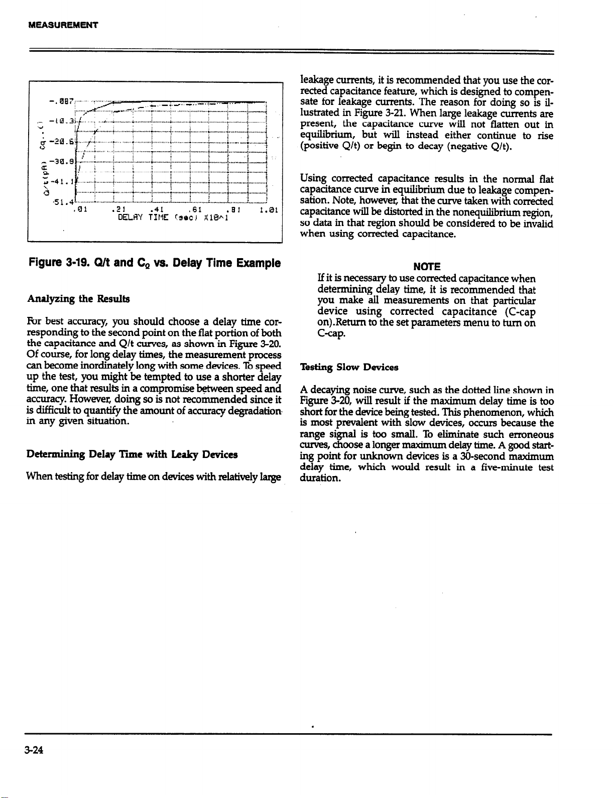
leakage currents, it is recommended that you use the corrected capacitance feature, which is designed to compen-
sate for leakage currents. The reason for doing so is illustrated in Figure 3-21. When large leakage currents are
present, the capacitance curve will not flatten out in
equilibrium, but will instead either continue to rise
(positive Q/t) or begin to decay (negative Q/t).
Using corrected capacitance results in the normal flat
capacitance curve in equilibrium due to leakage compensation. Note, however, that the curve taken with corrected
capacitance will be distorted in the nonequilibrium region,
so data in that region should be considered to be invalid
when using corrected capacitance.
Figure 3-19. Wt and Ca vs. Delay Time Example
Analyzing the Results
For best accuracy, you should choose a delay time corresponding to the second point on the flat portion of both
the capacitance and Q/t curves, as shown in Figure 3-20.
Of course, for long delay times, the measurement process
can become inordinately long with some devices. To speed
up the test, you might be tempted to use a shorter delay
time, one that results in a compromise between speed and
accuracy. However, doing so is not recommended since it
is difficult to quantify the amount of accuracy degradation
in any given situation.
Determining Delay Time with Lea@ Devices
When testing for delay time on devices with relatively large
NOTE
If it is necessary to use corrected capacitance when
determining delay time, it is recommended that
you make atl measurements on that park&r
device using corrected capacitance (C-cap
on).Retum to the set parameters menu to turn on
C-cap.
Testing Slow Devices
A decaying noise curve, such as the dotted line shown in
Figure 3-20, will result if the maximum delay time is too
short for the device being tested. This phenomenon, which
is most prevalent with slow devices, occurs because the
range signal is too small. To eliminate such erroneous
curves, choose a longer
nxcdmum delay time. A good starting point for unknown devices is a 30-second maximum
delay time, which would result in a five-minute test
duration.
3-24
.
Page 54

Capacitance
p
:
i
;
I
i
j
i
.....-...... Erroneous curve because
maximum delay time
\
too short
MEASUREMENT
Figure 340. Choosing Optimum Delay Time
C-Cap off.
- C-Cap on Distorts
Non-Equilibrium Curve
Positive Q/t
Negative Q/t
Figure 3-21. Capacitance and Leakage Current Using Corrected Capacitance
3-25
Page 55

MEASUREMENT
3.7 MAKING CV MEASUREMENTS
The following paragraphs describe procedures for making CV sweeps both manually, and automatically. During
a sweep, the following parameters are stored within an array for later analysis:
1. C, (quasistatic capacitance). C, is measured by the
Model 595.
2. Q/t (current), as measured by the Model 595.
3.
CH (high-frequency capacitance). High-frequency capacitance is measured at 1OOkHz or lMHz (depending on
the selected test frequency) by the Model 590.
4.
G (high-frequency conductance). The Model 590
measures the conductance of the device at lOOkHz or
lMHz, depending on the selected test frequency.
NOTE
When using series model, resistance will be stored
and displayed instead of conductance.
5.
V, (gate voltage). The gate voltage is measured by the
Model 590. Note that the gate voltage as it is used by
the computer is opposite in polarity from that displayed
ori the front panel of the Model 590 because of the gateto-substrate voltage convention used (gate terminal connected to INPUT; substrate terminal connected to
OUTFWT).
3.7.1 CV Measurement Menu
Fii 3-22 shows the menu for CV measurements. various
options on this menu allow you to program menu
parameters, manually start a CV sweep, automatically initiate the sweep, and access the analysis functions. These
options are discussed below.
3.7.2 Programming Measurement Parameters
1. Range for both quasistatic and high-frequency measurements (2oOpF or 2nF). The measurement ranges of both
the Models 590 and 595 are set by this parameter.
2. Frequency for high-frequency measurements (1DokHz
or IMHz). This parameter sets the operating frequency of the Models 590 and 5951.
3. Model (parallel or series). Model selects whether the
device is modeled as a parallel capacitance and conductance, or a series capacitance and resistance. Model
affects only high-frequency capacitance and conductance measurements. See the Model 590 Instruction
Manual for more details on using parallel or series
model.
4. Start V (-120 s V 1; 120). Start V is the initial bias
voltage setting of a CV sweep.
5. Stop V: (-I20 4 V s 120). Stop V is the final bias
voltage setting of a CV sweep.
6. Bias V Bias V is a static DC level applied to the device
during certain static monitoring functions such as
leakage level tests and determining device & and
delay time. Note that the voltage source value returns
to the Bias V level after Stop V at the end of the sweep.
7. T delay: (0.07 5 T 5 199.99~~). Note that the time
delyy be FyFlY
progmmmed to maintain device
~6urhbrmm durmg a sweep, as discussed m paragraph
. .
8. Step V: (lOmV, 2OniV, 5OmV, or lOOmV): Step V is the
incremental change of voltage of the bias stakase
form. The polarity of Step V is automatically SEEpending on the relative values of Start V and Stop V.
If Stop V is more positive than Start V, Step V is
positive; if Stop V is more negative than Start V, Step
V is negative.
9. C-Cap: (Corrected capacitance). Uses the corrected
capacitance program of the Model 595 when enabled.
C-Cap should be used only when testing leaky devices.
As discussed in paragraph 3.6, C-cap should be used
for device measurement if you found it necessary to
use C-cap when determining delay time.
10. Filter: Sets the Model 595 to Filter 2 when on, Filter
0 (off) when off.
Menu Selections
By selecting option 1 on the CV measurement menu, you
can access the parameter selection menu shown in Figure
3-23. (Parameters can also be set from the sweep menu by
ressing
P
allowing parameters:
‘W) This menu allows you to program the
3-26
NOTE
The filter may distort the quasistatic CV curve if
there are less than 50 readings in the depletion
region of the curve. Turning off the filter will increase reading noise by 2.5 times. See the Model
595 Instruction Manual for complete filter details.
Page 56

** Device Measurement and Analysis **
OPEN CIRCUIT SUPPRESS SHOULD PRECEDE EACH MEASUREMENT
1. Set Measurement Parameters
2. Manual Start CU Sweep
3. Auto Start CU Sweep
4. Analyze Sweep Data
5. Return to Main Menu
MEASUREMENT
Enter number to select from menu
Figure 3-22. Device Measumment Menu
3-27
Page 57
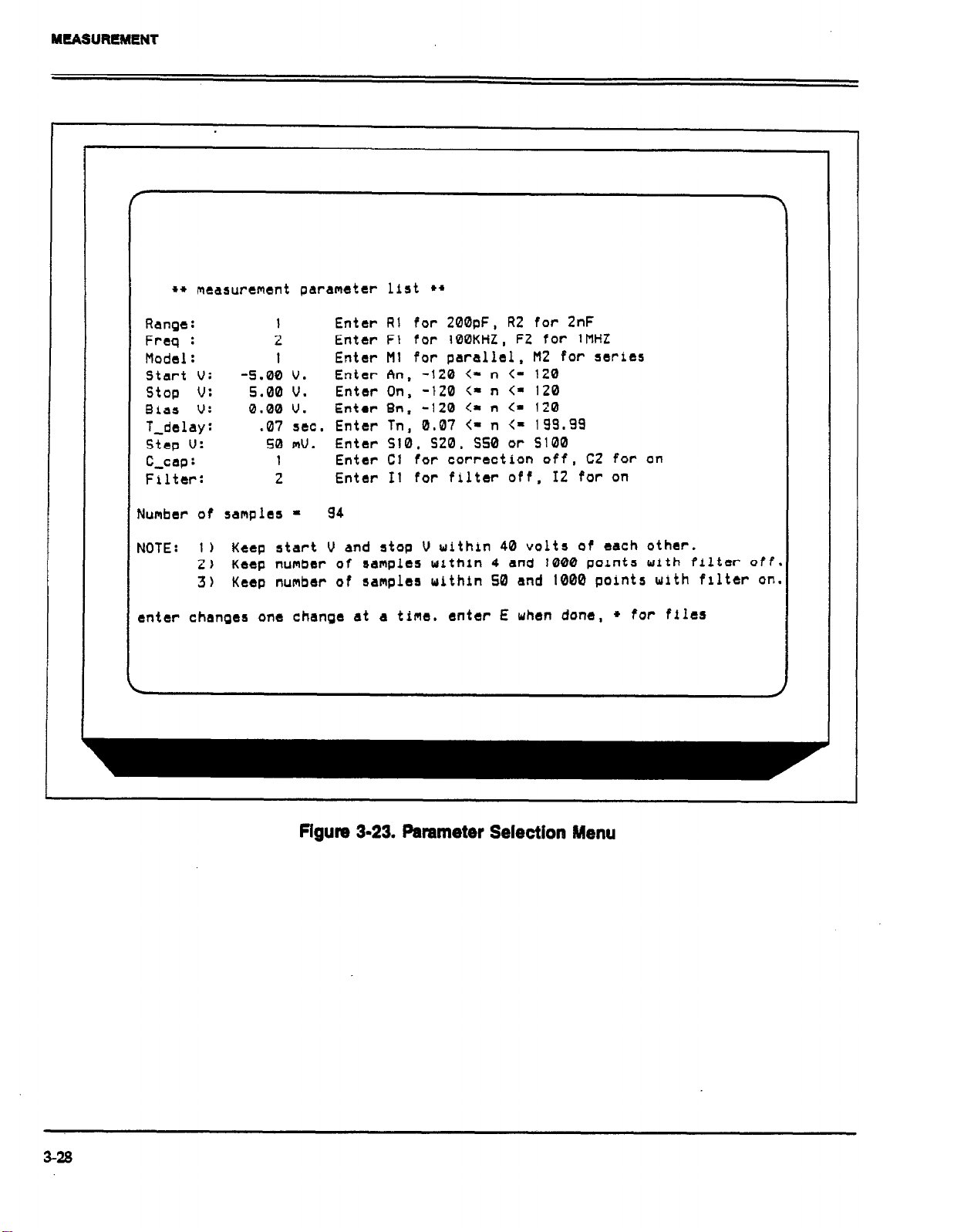
MEASUREMENT
l + measurement parameter list l *
Range:
~ Freq :
Model:
Start U: -5.00 v.
stop v: 5.00 v.
61as u:
T-delay:
Step V:
C-cap :
Filter:
Number of samples = 94
NOTE:
enter changes one change at a time. enter E when done, + for files
1) Keep start U and stop U within 40 volts of each other.
2) Keep number of samples within 4 and 1000 pornts with filter off.
3) Keep number of samples within SO and 1000 points with filter on.
1
2
1
0.00 v.
.07 sec.
50 mV.
1
2
Enter R1 for 200pF, R2 for 2nF
Enter Ft for IBOKHZ, F2 for 1MHZ
Enter Ml for parallel, HZ for series
Enter An, -120 <= n <= 120
Enter On,
Enter Bn, -120 <- n <- 120
Enter Tn, 0.07 <= n <= 199.99
Enter S10, S20, SSO or Sl00
Enter Cl for correction off, C2 for on
Enter I1 for filter off, 12 for on
-120 c- n <= 120
3-28
Flgure 3-23. Parameter Selection Menu
Page 58

MEASUREMENT
Determining the Number of Readings in a Sweep
The number of readings (bias steps) in a given sweep is
determined by Start V, Stop V, and Step V, as well as
whether or not the filter is enabled. The number of
readings is determined as follows:
R = INT [(ABS(Vs,~ - Vsm) I 2Vs,) - F ]
Where: R = number of readings in the sweep
INT = take the integer of the expression
ABS = take the absolute value of the expression
V
SrOr = programmed stop voltage
V
V
=I programmed start voltage
rr.4ARI
sTE.. = programmed step voltage
F - 2 if the filter is off
F = 6 if the filter is on
Example: Assume that Start V and Stop V are +lOV and
-#V respectively, and that Step V is lO0n-U. With the filter
on, the number of readings is:
R = INT((ABS(-IO-(10))/.2)-6
R = 94
Programming Considerations
When selecting parameters, there are a few points to keep
in mind, including:
1.
The maximum difference between the programmed
Start V and Stop V is 40V. Exceeding this value will
generate an error message.
2.
Voltage source polarity is specified at the gate with
respect to the substrate. For example, with a positive
voltage, the gate will be biased positive relative to the
substrate. Thus, an n-type material must be biased
positive to be in the accumulation region.
3.
Time delay must be carefuIIy chosen so that the device
remains in equilibrium throughout the sweep. The procedure to determine optimum delay time is covered in
paragraph 3.6. Failure to properly program proper delay
time wit1 distort quasistatic and high-frequency CV
curves. See paragraph 3.9 for additionaI measurement
considerations.
4.
The filter should be used only when more than 50
readings in the fundamental change area of the curve
are taken; see the Model 595 Instruction Manual,
paragraph 3.12 for more information. Note that the
parameter menu includes a note to remind you of the
.%-reading limitation because you will not be able to exit
the parameter menu with the filter on and ~50 points.
Programming Parameters
To program a parameter, type in the indicated menu let-
ter followed by the pertinent parameter. The examples
below will help to demonstrate this process.
Example 1: Select IMHz High-frequency Operation
To select high frequency operation, simply type in F2 at
the command prompt and press the ENTER key.
Example 2: F’rog~am a +I5V Bias V
Type in 815 and press the ENTER key.
Example 3: Select O.Isec Delay Time
Type in Xl.1 and press the ENTER key.
Example 4: Program a 20mV Step VoItage
Type in S20 and press the ENTER key.
Saving/Recalling Parameters
By pressing the “*l’ key, you can save or load parameters
to or from diskette. Press “s” (save) or 7’ (load) to carry
out the desired operation. You will then be prompted to
type in the filename to be saved or loaded. An error
message wiII be given if a file cannot be found or will be
overwritten.
When the save option is selected, the parameter values currently in effect wiIl be saved under the selected filename.
Parameters loaded from art existing file wiII be updated to
cm~orm to the new vdues.
Retuning to Previous Menu
After all parameters have been programmed (or Ioaded
from disk), press “E” to return to the previous menu.
3.7.3 Manual CV Sweep
Description
A manuaI CV sweep requires that you observe device
3-29
Page 59

MEASUREMENT
leakage, and then manually trigger the sweep. When
sweeping from inversion to accumulation, you must wait
for the device to attain equilibrium. An optional Iight can
be controlled to speed up the equilibrium process.
Procedure
1. Select the Manual Start CV Sweep option. The computer
will display the options in Figure 3-24.
2.Verifj a zero probes-up capacitance, and suppress if
necessary (press “r).
3. Press “M” and program the following parameters.
Range: As required for the expected capacitance.
Frequency: lOOkHz or lMHz as required.
Model: Parallel or series as required.
Start V: Accumulation or inversion voltage, as determined in paragraph 3.6.
Stop V: Inversion or accumulation voltage, as determin-
ed in paragraph 3.6.
T Delay: As required, to maintain equilibrium (See
paragraph 3.6)
Step V: Same as used when testing device in paragraph
3.6.
C-Cap: Off except for leaky devices (see paragraph 3.6).
Filter: On
4. If sweeping from accumulation to inversion, monitor the
current until it reaches the system leakage level;~ as
discussed in paragraph 3.4. When the current reaches
the system leakage level, press “s” to trigger the sweep.
5. If sweeping from inversion to accumulation, wait until
the device reaches equilibrium (equilibrium occurs when
Q/t decays to the system leakage level). If a light is connected to the system, press “I? to turn on the light to
speed up equilibrium. Turn off the light once equilibrium is reached prior to initiating the sweep (it may
take a few moments for the device to settle after tuming off the light). Press “s” to initiate the sweep.
6. The computer will then display a message that the
sweep is in progress. During the sweep, you can press
any key to abort, if desired.
Z l3Abwing the sweep, press ENTER to return to the
previous menu.
8. Select option 4 to view and analyze the data. Refer to
Section 4 for complete details on data analysis. Note that
&, area, and N,, values, as previously used in
analysis may not apply to this measurement, and may
require changing before analysis.
3.7.4 Auto CV Sweep
Description
The auto sweep procedure is similar to that used for
manual sweep, except that you can program the current
trip point at which the sweep will automatically begin.
Otherwise, the procedure is essentially the same, as outlined below.
Procedure
1. Select Auto Start CV Sweep. The computer will display
the options in Figure 3-25.
2. Verify a zero probes-up capacitance and suppress if
necessary, (press ‘73.
3. Press “IVY and program the following parameters.
Range: As required for the expected capacitance.
Frequency: lOOkI& or lMHz as required.
Model: Parallel or series as required.
Start V: Accumulation or inversion voltage, as determined in paragraph 3.6.
Stop V: Inversion or accumulation voltage, as determin-
ed in paragraph 3.6.
T Delay : As required to maintain equilibrium (See
paragraph 3.6)
Step V: Same as used when testing device in paragraph
3.6.
C-Cap: Off except for leaky devices.
Filter: On *
4. kess “G” and the type in the desired leakage trip point
when prompted to do so. Typically, this value will equal
the system leakage level, as determined in paragraph
3.4.
5. Press ‘T” to select above or below trip threshold.
6. If sweeping from inversion to accumulation, you can
turn on the light (if so equipped) to speed up
equilibrium by pressing “I?. Be sure to turn off the light
once equilibium is reached before initiating the sweep
(it may take a few moments for the device to settle after
turning off the light).
Z Press “K to arm the sweep. The computer will continue
to monitor readings while waiting for the trip point.
8. Once the leakage current reaches the trip point, the
sweep will be initiated. During the sweep, you can
press any key to abort the process.
9. Once the sweep is completed, press the ENl’ER key
to return to the previous menu.
10. Select option 4, Analyze CV Data, to view or graph the
data. Section 4 covers analysis in detail.
3-30
Page 60

l * manual start sweep measurement l *
Press ‘II’ to set measurement parameters.
Press ‘Z’ to suppress Cq, Ch, and G (probe up, suppress on).
Press ‘I?’ to monitor raw Cq, Ch. and G (probe up, suppress off ).
Press ‘L’ to toggle light on/off.
Press ‘S’ to start sweep.
Press ‘0’ to Ourt.
(note: Keyboard response tine is affected by delay time)
MEASUREMENT
Suppress is OFF.
Light drive is OFF.
Quasistatic :
High Creq :
Figure 3-24. Manual Sweep Menu
Cq (pF)
45.9
Ch (pF)
45.4
Sweep will take .4 minutes . .
a/t (pAt)
. 100
G (US)
-1.0000E+01
Start Ugs
1 .960
3-31
Page 61

l * auto start sweep measurement **
Press ‘M’ to set measurement parameters.
Press ‘Z’ to suppress Cq, Ch, and G (probe up, suppress on ).
Press ‘R’ to monitor raw Cq, Ch, and G (probe up, suppress off).
Press ‘T’ to toggle trigger region.
Press ‘G’ to set start-sweep threshold current.
Press ‘L’ to toggle light on/off.
Press ‘A’ to arm sweep.
Press ‘Q’ to Quit.
(note: Keyboard response time is affected by delay time)
Suppress is OFF.
Light drive is OFF.
km sweep is OFF.
Sweep will take .4 minutes.
Threshold current = 0 p,4
Trigger on >= threshold
Quasistatic f
High freq :
Cq ipF i Qit ipAj
46.0 0.000
Ch (pF) G (US)
45.4 -1.0000E+01
flgum 3-25. Auto Sweep Menu
Start Vgs
1.960
3-32
Page 62

MEASUREMENT
9.7.5 Using Corrected Capacitance
When making quasistatic measurements on leaky devices,
it is recommended that you use the corrected capacitance
function to compensate for leakage. Otherwise, the
resulting quasistatic CV curves will be tilted because of the
leakage resistance of the device or test system When using corrected capacitance, it is very important that the
device remain in equilibrium throughout the sweep. Data
taken in nonequilibriumwith corrected capacitance enabled should be considered to be invalid, and the resulting
curve will be distorted in the nonequilkium region of the
curve.
NOTE
If you found is was necessary to use corrected
capacitance when determining delay time
(paragraph 3.6), it is recommended that you also
use corrected capacitance when measuring the
device.
3.8 LIGHT CONNECTIONS
A user-supplied light can be connected to the system in
order to help attain device equilibrium in inversion more
rapidly. This light is controlled through appropriate terminals on the DIGITALUO port of the Model 5951 Remote
Input Coupler The following paragraphs dissuss DIGE4L
I/O port terminal assignments along with typical light
COMeCtiOIl.5.
the Model 230 Programming Manual.
OUTPUE OUTPUT is intended for controlling an external light source. Logic convention is such that OUTPUT
is LO when the software indicates that the light is ON.
Note that OUTPUT is LS-TTL compatible with a
guaranteed 8mA current sink capability.
Digital Common: Provides a common connection for external circuits.
Digital I/O Port
vi
12 11 10
9 8
I
Figum 3-26. Digltal I/O Port Terminal Arrangement
Table 3-2. Digital VO Port Terminal Assignments
7
3.8.1 Digital I/O Port Terminals
Table 3-2 summa&es the termir& assignments for the
DIGITAL I/O port of the Model 5951. Figure 3-26 shows
the pinouts for the supplied mating co~eclwr. Terminals
include:
+5V Digital (pins 1 and 2): +5V digital is supplied thmugh
an internal 33f2 resistor for shortxircuit protection. Cur-
rent draw should be limited to m to avoid supply
loading.
DigitaIInputs(pins36):Thesetemkalspassthroughthe
digital inputs to the Model 230-1. One possible use for
these inputs would be to monitor a test fixture closure
status switch. Note that the Package 82 software does not
tIy support reading the in
r
modified to do so, if desire r
puts can be read with the Ul command, as described in
tem&als,butitcould
. The status of these in-
Description
+5v Digital*
+5v Digital*
NC
*+5V sowed through internal 33Q resistor.
*Digital inputs passed through to Model 230-l
toutput controls lights HI = Opp; Lo = ON
3-33
Page 63

MEASUREMENT
3.8.2 LED Connections
The digital output has sufficient drive capability to directly drive LEDs up to 8mA using the connecting method
shown in Fii 3-Z The anode of the LED should be connected to +5V, and the cathode should be connected to
OUTPUT through a 3300 current-limiting resistor. Use of
LEDs that draw more than 8mA is not recommended.
.+5v 43 ,
3
Lad
Dl
0
Rl
33021
7
o”tputi10; <-
Digital I
common
Figurn 347. Dimct LED Control
Ill
1 i12:
I
5951
Digital
I/O Port
3.8.3 Relay Control
For larger LEDs, or for small incandescent lamps, an external relay control circuit can be used to switch the larger
current. Figure 3-28 shows a typical circuit. With the configuration shown, a normally-closed relay contact will be
necessary to ensure the light is on at the proper time. Note
that an external power supply will be necessary to drive
the external circuitry. The value of the base resistor will
depend on the current gain of the transistor as well as the
power supply voltage and relay coil resistance. For example, with a supply voltage of 5V, a coil resistance of 5OOf2,
and a current gain of loo, a base resistor value of lOk!I
should be adequate to drive the transistor into saturation.
Note that the diode across the relay coil should be included to protect the transistor from lAi/dt voltages when the
relay is de-energized.
3.9 MEASUREMENT CONSIDERATIONS
The importance of making tzarefd CV cum measurements
is often underestimated. However, errors in the CV data
will pmpogate through calculations, resulting in errors in
device parameters derived from the curves. These errors
can be amplified during calculations by a factor of Xl or
more.
With careful attention, the effects ob many common error
sourcesca.nbe
we will discuss some common error sources and provide
suggested methods for avoiding them.
minim&d. In the following paragraphs,
Page 64

Dl
MEASUREMENT
Digital
Figure 3-28. Relay Light Control
3.9.1 Potential Error Sources
Theoretically a capacitarxe measurement using one of the
common techniques would require only that two leads be
used to connect the measuring instrument to the device
under test @UT)-the input and output. In practice,
how- various parasitic or stray components complicate
the measuring circuit.
stray Capacitances
Regardless of the measurement frequency., stray
capacitances present in the circuit are important to consider Stray capacitances can cause offsets when they are
in parallel with the device, can act as a shunt load on the
input or output, or can cause coupling between the device
and nearby AC signal sources.
away from the input to ground. This phenomenon results
in capacitance gain error, with the CV curve results shown
in Figure 3-31.
When stray capacitance is in parallel with with the DUT,
it causes a capacitance offset, adding to the capacitance
of the device under test (C,,), as shown in Figure 3-29.
Shunt capacitance, on the other hand, often kreases the
noise gain of the intrumentation amplifiers, increasing
capacitance reading noise (Fii MO). Shunt capacitance
also forms a capacitive divider with Corn,, steering current
. . . . . . . . . . ..l.
Offset
Normal
Figure 3-29. CV Cuwe with Capacitance Offset
3-35
Page 65

MEASUREMENT
Figure 3-30. CV Curve with Added Noise
Leakage Resistances
Under quasistatic measurement conditions, the impedance
of CD, is almost as large as the insulation resistances in
the rest of the measurement circuit. Consequently, even
leakage resistances of lP?J or more can contribute signifi-
cant errors if not taken into consideration.
Resistance across the DUT will conduct an error current
in addition to the device current. Since this resistive cur-
rent is directly proportional to the applied bias voltage, and
the capacitor current is not, the result is a capacitance off-
set that is proportional to the applied voltage. The end
result shows up as a “tilt” in the quasistatic CV curve, as
shown in Figure 3-32.
. . . . . . . . . . . . . . .
With Gain
Normal
Error
Figure 391. CV Curve Resulting from Gain Error
Stray capacitance may also couple current or charge from
nearby AC signal sources into the input of the measuring
instrument. This noise current adds to the device current
and results in noisy, drifty, or unrepeatable measurements.
For quasistatic measurements, power line frequency and
electrostatic coupling are particularly troublesome, while
digital and RF signals are the primary cause of noise induced in high-frequency measurements.
---------a----- Tilted Curve Caused by
Leakage
Normal
Figure 3-32. Curve Tilt Caused By Voltage!-
dependent Leakage
Stray resistance to nearby fixed voltage sources results in
a constant (rather than a bias voltage-dependent) leakage
current. Other sources of constant leakage curren
ts include
instrument input bias currents, and electrochemical currents caused by device or fixture contamination. Such con-
stant leakage currents cause a voltage-independent
capacitance offset.
3-36
Page 66

MEASUREMENT
Keep in mind that insulation resistance and leakage current are aggravated by high humidity as well as by contaminants. In order to minimize these effects, always keep
devices and test fixtures in clean, dry conditions.
High-Frequency Effects
At measurement frequencies of approximately lOOkI& and
higher, the impedance of CDoI may be so small than any
series impedance in the rest of the circuit may cause errors. Whether such series impedance is caused by inductance (such as from leads or probes), or from resistance
(as with a high-resistivity substrate), this series impedance
causes non-linearity in the measured capacitance. The
resulting CV curve is, of course, affected by such non-
Iinearity, as shown in Figure 3-33.
----------
--..
AC
errors to an acceptable level. Once most of the error saurces
have been
minimized, any residual errors can be further
reduced by using the probes-up suppression and corrected
capacitance features of the Package 82 software.
Key details that require attention include use of proper
cabling and effective shielding. These important aspects
are discussed below.
Cabling Considerations
Cables must be used to connect the instruments to the
device under test. Ideally, these cables should supply the
test voltage to the device unaltered in any way. The test
voltage is converted into a current or charge in the DUT,
and should be carried back to the instruments undisturbed. Along the way, potential error sources must be
minimized.
I
Coaxial cable is usually used in order to eliminate stray
capacitance between the measurement leads. The cable
shieId is connected to a low-impedance point (guard) that
follows the meter input. This technique, known as a thme-
terminal capacitance measurement, is almost universally
used ln commexial instrumentation. The shield shunts
current away from the input to the guard.
c
V
-------------- With Nonlinearity
b
Normal
Figure 3-33. CV Curve Caused By Nonlinearity
mother high-frequency effect is caused by the AC network
xmed by the instrumentation, cables, switching cimuits,
and the test fixtures. Referred to as transmission line error sources, the network essentially transforms the impedance of CDur when it is referred to the input of the instrument, altering the measured value. Transmission line
effects alter the gain and produce non-linearities.
3.9.2 Avoiding Capacitance Errors
The many possible error sources that can affect CV
measurements may seem like a great deal to handle.
However, careful attention to a few key details will reduce
Coaxial cables also sewe as smooth transmission lines to
carry high-frequency signals without attenuation. For this
reason, the cable’s characteristic impedance should close-
ly match that of the instrument input and output, which
is usually 500. Standard RG-58 cable is adequate for lie-
quencies in the range of lkH2 to more than IOMHZ. High-
quality BNC connectors with gold-plated center conductors reduce errors from high series contact resistance.
Quasistatic CV measurements are susceptible to shunt
resistance and leakage currents as well as to stray
capacitances. Although coaxial cables are still appropriate
for these measurements, the cables should be checked to
ensure that the insulation resistance is sufficiently high
( >10i2Q). Also, when such cables are flexed, the shield
rubs against the insulation, generating small currents due
to triboelectric effects. These currents can be minimized
by using low-noise cable (such as the Model 4801) that is
lubricated with graphite to reduce friction and to dissipate
generated charges.
Flex-producing viition should be eliminated at the
source whenever possible. If vibration cannot be entirely
eliminated, cables should be securely fastened to prevent
flexing.
3-37
Page 67

MEASUREMENT
Once final point regarding cable precautions is in order:
Cables can only degrade the measurement, not improve
it. Thus, cable lengths should be minimized where possible, without straining cables or connections.
Device Connections
Care in properly protecting the signal path should not stop
at the cable ends where the connection is made to the DLJT
fixture. In fact, the device connection is an extremely important aspect of the measurement. For the same reasons
given for coaxial cables, it is best to continue the coaxial
path as close to the DUT as possible by using coaxial probes. Also, it is important to
minimize stray capacitance and
maximize insulation resistance in the pathway from the
end of the coaxial cable to the DUT
Most devices have one terminal that is well insulated from
other conductors, as in the gate of an MOS test dot. The
input should be connected to the gate because it is more
susceptible to stray signals than is the output. The output
can better toierate being connected to a terminal with high
shunt capacitance, noise, or poor insulation resistance,
although these characteristics should still be optimized for
best results.
0ffSd.S
Offset capacitance and conductance caused by the test apparatus can be eliminated by performing a suppression
with the probes in the up position. These offsets will then
be nulled out when the measurement is made. Whenever
the system configuration is changed, the suppression procedure should be repeated. In fact, for maximum accuracy,
it is recommended that you pedorm a probes-up suppression or at least verify prior to every measurement.
Gain and Nonlinearity Jkors
Gain errors are difficult to quantify. For that reason, gain
correction is applied to every Package 82 measurement.
Gain constants are determined by measuring accurate
calibration sources during the cable correction process.
Nonlinearity is normally more difficult to correct for than
are gain or offsets errors. The cable correction process that
is part of the Package 82, however, provides nonlinearity
compensation for high-frequency measurements, even for
nonideal configurations such as switching matrices.
Voltage-Dependent Offset
Test Fixture ShieIdlng
At the point where the coaxial cable shielding ends, the
sensitive input node is exposed, inviting error sources to
interfere. Proper device shielding need not end with the
cables or probes, howevez if a shielded test fixture is used.
A shielded fin=.- somethes kamwn as a Faradaa cage;
-- w-v, -
consists of a metal enclosure that completely surrounds
the DUT and leads. In order to be effect&, the shield must
be electrically connected to the coaxial shield. ‘@epically,
bulkhead connectors are mounted to the side of the cage
to bring in the signals. Coaxial cables should be continued
inside, if possible, or individual input and output leads
should be widely spaced in order to maintain inputloutput isolation.
3.9.3 Correcting Residual Errors
Controlling errors at the source is the best way to optimize
CV measurements, but doing so is not always possible.
Remaining residual errors include offset, gain, noise, and
voltage-dependent errors. Ways to deal with these error
sources are discussed in the following paragraphs.
kltage-dependent offset (curve tilt) is the most difficult
to correct error associated with quasistatic CV
measurements. It can be eliminated by using the corrected
capacitance function of the Padra’ge 82 software. In this
technique, the current flowing in the device is measured
as the capacitance value is measured. The current is known
as Q/t because its value is derived from the slope of the
charge integrator waveform. Q/t is used to correct
capacitance readings for offsets causedby shunt resistance
and leakage currents.
Care must be taken when using the corrected capacitance
feature, however When the device is in nonequilibrium,
device current adds to any leakage current, with the resuh
that the curve is distorted in the nonequilibrium region.
The solution is to keep the device in equilibrium
tbroughoutthesweepbyca&ullychoosingthe delaytime.
Curve Misalignment
At times, quasistatic and high frequency curves may be
slightly misaligned due to gain errors or external factors.
In such cases, curve gain and offset factors can be applied
to the curves to properly align them. This feature is
available under the analysis menu.
3-38
Page 68

MEASUREMENT
Noise
Residual noise on the CV curve can be minimized by using filtering when taking your data. Care must be taken,
however, not to apply too much filtering, as doing do will
distort the curve. Often, some experimentation may be
necessary to optimize noise reduction and at the same time
keep undesirable effects to a minhnum. A good rule of
thumb is to use the filter only when there are more than
50 points taken over the fundamental change in the data
curve. The filter is selectable in the parameter menu.
3.9.4 Interpreting CV Cures
Even when all the precautions outlined here are followed, there are still some possible obstacles to successfully
using CV curves to analyze semiconductor devices.
Semiconductor capacitors are far from ideal, so care must
be taken to understand how the device operates. Also, the
curves must be generated under well-controlled test conditions that ensure repeatable, analyzable results.
MaWining Equilibrium
The condition of the device when all internal capacitances
are fully charged is referred to as equilibrium. Most
quasistatic and high-frequency CV curve analysis is based on the simplifying assumption that the device is
measured in equilibrium. Internal RC time constants limit
the rate at which the device bias may be swept while maintaining equilibrium. They also determine the hold time required for device settling after setting the bias voltage to
a new value before measuring CDvr.
The two main parameters to be controlled, then, are the
bias sweep mte and the hold time. When these parameters
are set properly, the normal CV cmves shown in Fi3-34 result. Once the proper sweep rate and hold time have
been determined, it is important that all curves compared
with one another be measured under the same test conditions; otherwise, it may be the parameters, not the
devices themselves, that cause the compared curves to
Accumulation Depletion
Inversion
Quasistatic
v substrate
Figure 3-34. Normal CV Curve Results when Device is Kept in Equilibrium
3-39
Page 69

MEASUREMENT
Analyzing Curves for Equilibrium
There are three primary indicators that can be used to
determine whether a device has remained in equilibrium
during testing. First, as long as a device is in equilibrium,
CD, is settled at all points in the sweep. As a result, it
makes no difference whether the sweep goes from ac-
cumulation to inversion, or from inversion to accumula-
tion, nor does it matter how rapidly the sweep is perform-
ed. Therefore, curves made in both directions will be the
same, exhibiting no hysteresis, and any curve made at a
slower rate will be the same. Figure 3-35 shows the type
of hysteresis that will occur if the sweep rate is too fast,
and the device does not remain in equilibrium.
The second equilibrium yardstick requires that the DC current through the device be essentially zero at each
measurement point after device settling. This test can be
performed by monitoring Q/t. Thirdly the curves should
exhibit the smooth equilibrium shape. Deviations from the
ideal smooth shape indicate a nonequilibrium condition,
as in the examples resulting from too short a hold time
shown in Figure 3-36. Note that at least two of these indicators should be used together, if possible, because any
of the three used alone can be misleading at times.
One final quick test to confirm equilibrium is to observe
C, during a hold time at the end of the CV sweep from
accumulation to inversion. During this finaL hold time, the
capacitance should remain constant. If a curve has been
swept too quickly, the capacitance will rise slightly during the final hold time.
Initial Equilibrium
begin the sweep in the accumulation region of the curve
whenever possible.
Still, it is often necessary to begin the sweep in the inver-
sion region to check for curve hysteresis. In this case, a
light pulse, shone on the device, can be used to quickly
generate the minority carriers required by the forming inversion layer, thus speeding up equilibrium and shortening the hold time.
The best way to ensure equilibrium is initially achieved is
to monitor the DC current in the device and wait for it to
decay to the DC leakage level of the system. A second in-
dication that equ.ihbrium is reached is that the capacitance
level at the initial bias voltage decays to its equilibrium
level.
3.9.5 Dynamic Range Considerations
The dynamic range of a suppressed quasistatic or high-
frequency measurement will be reduced by the amount
suppressed. For example, if, on the 2OOpF range, you were
to suppress a value of lBpF, the dynamic range would be
reduced by that amount. Under these conditions, the max-
imum value the instrument could measure without
overflowing would be l9OpF.
A similar situation exists when using cable correction with
the Model 590. For example, the maximum measurable
value on the 2nF range may be reduced to 1.8nF when us-
ing cable correction. The degree of reduction will depend
on the amount of correction necessary for the particular
test setup.
Biasing the device to the starting voltage in the inversion
region at the beginning of a CV measurement creates a
nonequilibrium condition that must be allowed to subside
beforetheCVsweepbegins.Thisrecoverytoequilibrium
can take seconds, minutes, or even tens of minutes to
achieve. For that reason, it is generally advantageous to
The dynamic range of quasistatic capacitance
measurements is reduced with high Q/t. The maximum
Q/t value for a given capacitance value depends on both
the delay time and the step voltage. See the Model 595
Instruction Manual Specifications for details.
Page 70

MiASUREMENT
A. QUASISTATIC
8. HIGH FREQUENCY
Figure 3-35. Curve #hysteresis Resulting When Sweep is Too Rapid
-a----m--e--. S h 0 rt
Hold Time
Normal
A. QUASISTATIC
6. HIGH FREQUENCY
Figure 3-36. Dlstortion When Hold Time is Too Short
34m-42
Page 71

SECTION 4
Analvsis
4.1 lNfRODUCl=lON
This section covers the various analysis features of the
Package 82 softw;ue. References and suggested reading are
also included at the end of the section.
Infbrmation concerning equipment setup and measure-
ment techniques may be found in Sections 2 and 3.
Section 4 information is arranged as follows:
4.2 Constanb and Symbols Used for Analysis: Discusses
the numerical constants and mathematical symbols
used in this section and by the Package 82saftwaze.
43 Obtainhg Information from Basic CV Cuwes:
Details how to obtain important information such as
device type and & from CV curves.
4.4 AnaIyzing CV Data: Discusses loading/saving
reading data, graphing reading data, and graphicai
and mathematical analysis.
4.5 Mobile Ionic Charge Concentration Measurement:
Discusses two methods to measure the mobfie ionic
charge concentration in the oxide of an MOS device.
4.6 References and Bibliography of CV Measurements
and Related Topics: Lists references used in this sec-
tion, along with add2iona.I texts and papem for suggested reading on CV measurement and analysis
topics.
4.2 CONSTANTS AND SYMBOLS USED FOR
ANALYSfS
4.2.1 Constants
J
These constants are declared at the top of the program
listing and are Wialized for silicon and silicon dioxide.
The constants can be re-defined for other material types,
if desired.
q - L&O239 x ltYqC. q is the fundamental unit of charge
on an electron given in coulombs.
kT - 4.046 x lo-l*J. kT represents thermal energy and is
defined at room temperature (293%).
eax = 3.400 x WSFkm. eox is the permittivity of silicon
dioxide.
- 1.04 x &i2Flcm. es is the permittivity of silicon.
es
E. - lS2eV. E. is the energy gap of silicon from valence
band to conduction band edge. Ideally no energy states
?tIdkMdh&pp.
fi = 1.45 x W cm+. n, is the intrinsic ctim concentra-
tion per cm3 in 25°C silicon.
4.2.2 Raw Data Symbols
The following symbols are used for data measured and
sent by the Models 590 and 595. Cp is interpolated from
C, so that C’p and CH are values at the same bias voltage.
csf
G
G
Qjt
VI3
High-frequency capacitance, as measured
by the Model 590 at either lO0kH.z or
z&atic capacitance measured by the
Model 595. &’ is interpolated from &’ so
that Ce’ and C, are values at the same bias
voltage.
High-frequency conductance, as measured
by the Model 590 at either lOOkI& or
lAa-Iz.
Current measured by the Model 595 at the
end of each capacitance measurement with
the tit in the capacitance fun&on.
Wtage reading sent by Wdel 590 with
matching C, and G,,.
Constants used by the Package 82 are summarized b&w.
41
Page 72
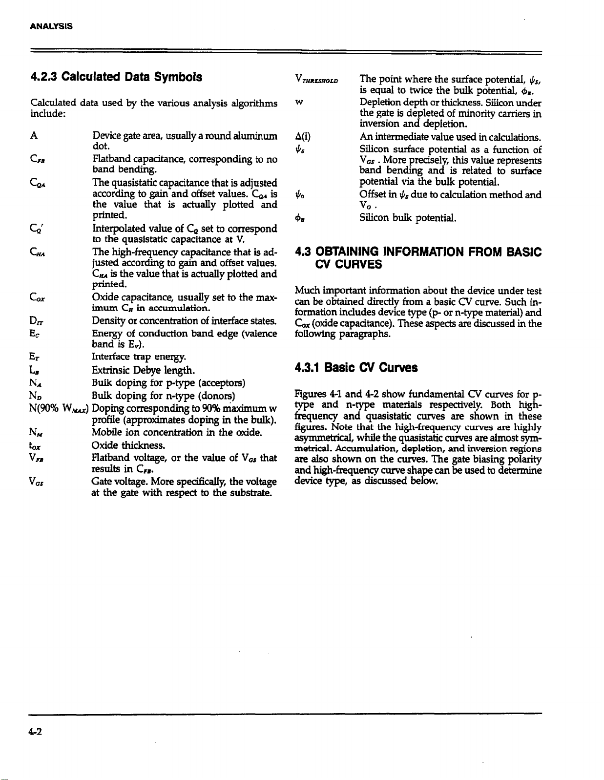
4.2.3 Calculated Data Symbols
Calculated data used by the various analysis algorithms
include:
A Device gate area, usually a round aluminum
dot.
C
SD
GA
c,
GA
cox
07
EC
ET
LB
N*
ND
N(90% W,) Doping corresponding to 90% maximum w
NM
bx
VFB
V
GS
Flatband capacitance, corresponding to no
band bending.
The quasistatic capacitance that is adjusted
according to gain and offset values. C, is
the value that is actuaIly plotted and
printed.
Interpolated value of C, set to correspond
to the quasistatic capacitance at V.
The high-frequency capacitance that is ad-
justed according to gain and offset values.
CHA is the value that is actually plotted and
printed.
Oxide capacitance, usually set to the max-
imum CH in accumulation.
Density or concentration of interface states.
Energy of conduction band edge (valence
band is Ev).
Interface trap energy.
Extrinsic Debye length.
BuIk doping for p-type (acceptors)
Bulk doping for n-type (donors)
profile (approximates doping in the bulk).
Mobile ion concentration in the oxide.
Oxide thickness.
Flatband voltage, or the value of V,, that
resllits in c,.
Gate voltage. More specifIcalIy, the voltage
at the gate with respect to the substrate.
V
THRESHOLD
The point where the surface potential, &,
is equal to twice the bulk potential, &.
W
Depletion depth or thickness. Silicon under
the gate is depleted of minority carriers in
inversion and depletion.
A(i)
4s
An intermediate value used in calculations.
Silicon surface potential as a function of
V
. More precisely this value represents
GS
band bending and is related to surface
potential via the bulk potential.
$0
Offset in & due to calculation method and
V
4%
!&on bulk potential.
4.3 OBTAINING INFORMATION FROM BASIC
CV CURVES
Much important information about the device under test
can be obtained directly from a basic CV curve. Such information incdudes device type (p- or n-type material) and
C, (oxide capacitance). These aspects are discussed in the
following paragraphs.
4.3.1 Basic CV Curves
Figures 4-l and 4-2 show fundamental CV curves for ptype and n-type materials respectively. Both highfrequency and quasistatic curves are shown in these
figures. Note that the high-frequency cmves are highly
asymmticai, whiIe the quasistatic curves are almost symmetrical. Accumulation, depletion, and inversion regions
are also shown on the curves. The gate biasing poiarity
and high-frequency curve shape can be used to determine
device type, as discussed below.
42
Page 73

Capacitance
ANALYSIS
inversion
Accumulation
Onset of Strong Inversion
CH
- %s
:
f
1
VFB
i i
: :
! ;
i i
VMEskciD
GATE BfAS VOLTAGE, V,,
Figure 4-l. CV Characteristics of p-type Material
+bS
4-3
Page 74

ANALYSS
Capacitance
- “GS VlHESKLD “FB
GATE BIAS VOLTAGE, VGS
Figure 4-2. W. Characteristics of n-type Material
4.3.2 Determining Device vpe
The semiconductor conductivity type (p or n dopant ions)
can be determined from the relative shape of the CV
curves. The high-frequency curve gives a better indication
than the quasistatic curve because of its highly asymmetrical nature. Note that the CV curve moves from the
accumulation to the inversion region as gate voltage, VW ,
becomes more positive for p-type materials, but the curve
moves from accumulation to inversion as V, becomes
more negative with n-type materials (Nicollian and Brews
372-374).
Accumulation
t
+“GS
4.4 ANALYZING CV DATA
A number of operations can be performed on sweep data
stored in a reading array including: saving or loading
reading data to or from disk, displaying or printing reading
data, graphing or plotting reading data, as well as
mathematical analysis of doping profile, flatband calcuiations, and interface traps. The following paragraphs
discuss analysis operations available with the Package 82
software.
4.4.1 Plotter and Printer Requirements
In order to determine the material type, use the following
rules:
1. If CH is greater when V,, is negative than when Var is
positive, the substrate material is p-type.
2. If, on the other hand, CM is greater with positive V,
than with negative VW, the substrate is n-type.
3. The end of the curve where C,, is greater is the accumulation region, while the opposite end of the curve
is the inversion region. The transitional area between
these two is the depletion region. These areas are marked on Figures 4-l and 4-2.
44
Phttex
A plotter can be used to obtain hard copy graphs. The
Package 82 software supports only plotters that use HP-
GL graphics language. Only IEEE-488 plotters can be used.
The plotter must be set to the addressable mode with a
primary address of 5. The plotter must, of course, be connected to the IEEE&XI bus of the computer using a suitable
IEEE-488 cable. A shielded IEEE-488 cable should be used
to avoid possible interference with other equipment.
Page 75

ANALYSIS
Printer
A printer can be connected to the IEEE-488 bus to provide
hardcopy printout of data. Note that the printer must be
set to a primary address of 1. For the IBM AT, a printer
can also be used with the parallel or serial port as long
as the print path was changed (see paragaph 2.7.)
NOTE
Use the HP BASIC “DUMP GRAPHICS” or
“DUMP ALPHA’ statements to obtain a hard copy
of any screen.
4.4.2 Analysis Menu
Figure 43 shows the analysis menu. You can access this
f
l * SWEEP DI’+TA ANALYSIS l *
1. Save Measurement Data Array to File
2. Load Measurement Data Array from File
3. Display Data Arrays
4. Display Analysis Constants
5. Graph Quasistatic C vs. Gate Voltage
6. Graph High Frequency C VI. Gate Voltage
7. Graph Both Cq and Ch vs. Gate Voltage.
8. Graph Q/t Current vs. Gate Voltage
9. Graph Conductance vs. Gate Voltage
10. Graph Doping Profile vs. Depth
11. Graph Oepth vs. Gate Voltage
12. Graph l/Ch^2 vs. Gate Voltage
13. Graph Dit vs. Energy
14. Graph Band Bending vs. Gate Voltage .
15. Graph Quasistatic C vs. Band Bending
16. Graph High Frequency C vs. 8and Bending
17. Return to Previous Menu
menu either by selecting option 6, Analyze CV Data, on
the main menu, or through most other submenus.
Key operations available on the menu include:
l Saving or loading array data to or from disk.
l Displaying (CRT) or printing (external printer) reading
or graphics array data.
l Displaying or modifying numerical values such as &,
tar, and N (doping concentration).
l Graphing or plotting reading array data.
l Graphical and mathematical analysis of the data array
\
Enter number to select from menu
Figure 4-3. Data Analysis Menu
45
Page 76

ANALYSIS
4.4.3 Saving and Recalling Data
By selecting option 1 or 2 you can save the current reading
array to diskette, or load previously taken readings from
diskette into the reading array. In addition to the array
elements (C, CH, Q/t, G, and V,), the following numerical
values are saved with the array: C&, A, tax, Step V, N,
and graph offset and gain values.
NOTE
Loading reading from diskette will overwrite any
data currently stored in the reading array. Data
analysis and graphing is always carried out on data
currently stored in the reading array.
Saving the Reading Array
Use the following procedure to save sweep data presently
stored in the reading array.
1.
Select option 1 on the analysis menu.
2.
The computer wilI display the current disk directory.
3.
XXI will then be prompted to type in the desired filename. Be sure to choose a name not on the present
d.&CtOry.
4
Next you will be prompted to enter header information,
up to a maximum of 160 characters. This feature can be
used to enter important information about the data-you,
are saving. For example, you may wish to enter the type
of device, the date, and the time the data was taken for
future reference.
5.
After entering header information, you wil.l be given one
last opportunitv to change it.
6.
If the header mrormation is correct, respond affirmatively to store the reading array to disk. Once storage is cornplete, you will be returned to the analysis menu.
Loading the Reading Array
4. The header information will be displayed after the file
is loaded.
5. To return to the analysis menu, press ENTER.
4.4.4 Displaying and Printing the Reading and
Graphics Arrays
By selecting option 3 on the analysis menu, you can
display array data on the computer CRT or print out that
array data for hardcopy. In order to print the data, you
must, of course, have a printer connected to the IEEE-488
bus. When displaying array data, the screen will be cleared
before arrays are displayed.
Note that you can display or print either reading or
graphics array data by selecting the appropriate option on
the submenu. The displayed and printed reading array
data includes the reading number; quasistatic capacitance,
current (Q/t); and high-frequency capacitance, conductance, and gate voltage. An example is shown in Fii 44.
NOTE
The quasistatic and high-frequency capacitance
values that are plotted, printed, and used in
calculations are first corrected for gain and offset
(paragraph 4.4.6) to obtain C, and CHA (adjusted
capacitance).
Graphics array data includes depletion depth, doping con-
centration, band bending interface trap energy, l/P, and
interface trap density. An ewmple is shown in Figure 45.
NOTE
Values of lP “flag” invalid data as explained in
paragraph 4.4.8.
Use the procedure below to recall data from diskette and
store it to the reading array. Remember that any data
presently in the reading array will be overwritten by the
data loaded from diskette.
1. Select option 2 on the analysis menu. The computer wilI
then display the current disk directory.
2. At the prompt, type in the desired filename and press
ENTER.
3. If the file exists, the reading array will be filled with the
data from the file; howevq an error message wiU be
given if the file does not sdst, or if it is of the wrong
type.
4-6
When displaying data on the CRT, you have the option
of selecting the first reading number to display.
lb rint only a portion of the array, display that portion
an then use the BASIC “DUMP ALPHA’ statement.
x
Changing the Graphics Window
The graphics window defines the contiguous array area
to be plotted. To change the graphics range (select graphics
window), seledion option 3 on the analysis menu, then
option 5 on the subsequent menu. The present graphics
Page 77

l0-30000'1- I
I0+3t0LL'f 10-30008'1
10+3SSSL'S 00+30000'0 00+38800'8 8
10+300~8'5
18+300~8'5 10+3tLSL'5 00+30000'0 LB-30000'I- :
I0+300?8'S 10+30991'S 00*30000'0 l0-30000'1- f
10+300fa's 10t39991'5 10-30000'1 i0-30000'1- V
10+300E8'5 10+38t9L’9 10-30800'1 00t30000'0 5
888’5
888'1
869'? 10+380f8'S 10+3029L'S 00+30000'8 00+30000'0 9
BBV'? 10+300f8'5 IBt35LSL'5 00+30000'0 00+30008’0 L
BE:'* 10+30028'S
0E.@'V 10+300:6'S 10+35V5L'5 00+30000'0 00+30800'a 6
068'E 10+30028'5 10+30SSL'S 00+30000'0 10-30888'1- 01
ICW300tE'S lB+30BSL'5 00t30000'0 IB-30880'1- II
10t30019’5 18+3BEtL’5 80+38800'0 00+38800'0 :I
10+30008'S 10+3ltEL'S 88+30008'8 80+30000'0 Cl
lBt30008'5 10+3E9ZL'5 00+30000'0 88+30000'0 VI
10-30000'1- 91
10+30091'S 10+3LLlL'S 18-30000'1 00t30000'0 51
lBt3009L'S 18t3LE69.5 06+30008'0 1&30080'l- LI
IB+30019'5 lBt35EES'S 08+30000'0 00+30008'0 Bi
liW3006t'S t@+3B99?‘5 10-30000'1 00+38000'0 2:
10+3002?'s te+35LBE’S 10-30000’1 09+38088’9 EZ
t0+3889E'5 10t3S~Zf'S 80t30000'0 10-30008'1- tZ
let300eE's 18+32992's 80+38000'0 ie-3000fl'I- 52
10+300t2'5 lOt3L602'5 80+30000'1 le-30060'I- 9:
10t30081'5 I8t35251'5 16-30008'1 10-3BB00'1- LZ
10+30011'S lW3006a'S 00+30000'kl 10-30660'1- 62
10+300?0'5 1@+31910'5 Be+Pa006'0 l&J-3aae6'1- 62
lBt300E6't 10+36026't Fl0+30000*0 I@-3BB00'2- BE
099-E
08V.S
BBZ'E
060-E
069'2
069': 10+380LL'S 10+30EEIL'5 t0-30000'1
00'2
08Z'Z 18+300fL'5 10t38819'5 60+30000'0 la-30080'1- 9I
BEB'Z 10+30099-5 lBt3BEE9'S 10-30800'1 0W30000'8 61
09e.1
$R9' I 10+308L5'5 IW3BZZS'S 00+30000'0 88+38800'8 li
B9T'l
BEE' I
6EB'I
088 *
M9'
OW'
eat-
080'
011'-
Page 78

ANALYSIS
j 0.80806400 I.%000E+50 -8.65046-02 -3.8561E-01 2.9321G04 l.BBBBE*SB
: 0.0800E*00 I.0000Er50 -8.40l:E-02 -3.83128-01 2.3321E-64 1.0000E+SB
3 0.0000E+00 1.0000E+50 -B.i479E-0’ -3.8059E-0f :.932lE-64 I.BBBBE+E.0
4 3.0546E-03 1.0000E+3.0 -?.8960E-82 -3.7807E-01
2.942lE-04 -1.8392Ec13
3 6.1197E-03 1.0000E+50 -6.7984E-02 -3.6709E-01
9 6.il97E-03 1.0000E+50 -6.50566-0
I0 6.119iE-03
II 6.1197E-03 1.0620E+17 -5.8993E-0i
1: 9.1953E-03 7.6700E+16 -5.5637E-02 -3.5474E-01 2.9624E-04 -4.9235E+IZ
13 l.?26:E-02
I.X82E-0: 3.3127E+l6 -4.81156-02 -3.47:2E-01
iB 3.4167E-82 6.8884E*lS -?.8579E-0:
13 5.8164E-02 7.0390E+lS -2.1430E-0:
:a 6.319BE-02 3.8720E+l5 -I .2706E-02 -
1,3800E-61 3.3747E+I5
l.E000E+50 -6.:0756-02 -3.6118E-01 2.9523E-04 -6.1980E+l:
I.0000E+S0 -5.:010E-02 -3.§ll:E-01 :.97*7E-e4 -3.3115E+I~
l.?l02E+l6 -4.3928E-02 -3.43046-01
4.5519E+16 -3.5409E-0’ -3.3652E-01
1.3869E*16 -:.440lE-02 -3.335lE-01 3.0i4fE-04 -I.Z853E+IZ
-I.B408E-03 -3.0095E-01 3.2’32E-04 -I.l742E+II
:.68lSE-02 -:.7:‘9E-01 3.404lE-04 -3.6402E+l0
:.4324E+lS 1.09;56-01 -I.B966E-01
:.38:4E+lS 1.3493E-01
!.X::E+lS 1.6335E-31 -1.3596E-01 3.9368E-04 -7.73366+09
l.B?36E+l5 1.946:E-01 -I.04486-BI 4.1144E-04 -2.3538Et09
2 -3.6416E-01 2.9523E-04 -B.l537E+12
-3.5610E-0t 2.9523E-04 -8.278?E+l:
-3.:76SE-01 3.04578-84 -6.6300EclT
-3.:060E-01 S.0996E-B)4 -3.%208E+lI
3.118lE-01 3.1437E-04 -:.344SE+l!
-2.6779E-01 3.3176E-04 -5.4:IIE+fB
-2.3499E-01 3.5600E-04 -2.3186E+l0
-I.6418E-01 3.8:96E-04 -3.7760E+09
2.3523E-04 -8.1313E+l:
:.9727E-04 -3.4503Etl2
:.9933E-04 -1,8066E+12
3.0036E-04 -1.4278Ecl’
?.7:68E-04 -l.,90!E+I0
4-8
Figure 4-5. Example of Graphics Army Print Out
Page 79

ANALYSIS
4.4.5 Graphing Data
Selecting a graphing option will cause a graph to be
generated on the screen, along with the graphics control
window.
NOTE
A particular graph retains its configuration until
a new reading array is analyzed.
The graphics control menu is shown in Figure 4-6 Through
this menu you can select the following:
1. Auto Scaling. When auto scaling is selected, the mini-
mum and maximum values for the data will automatic-
ally be used as the limits for both X and Y axes.
2. Axes Limits. This option allows you to select the mini-
mum and maximum limits for both X and Y axes, and
it can be used to zoom in on a portion of the curve. At
the prompt, type in Xmin, Xmax, Ymin, and Ymax separated by commas. To leave a parameter unchanged,
simply type in a comma at that position. Note that the
graph can be reversed top to bottom or right to left by
intedanging
also paragraph 4.4.5 for using the graphics window as
maximum and minimum limit values. See
an alternative.
3. Plot Graph. This option dumps the complete graph including the curve and axes to the plotter. Note, however,
that the graphics control menu will not appear on the
hard copy plot. “DUMP GRAl?HICS” can be used to
dump the graphics screen to a compatible printer. To
do so, pause the program, “DUMP GRAPHICS”, then
continue the program.
4. Plot Curve. Use this option to generate the curve only
on the external plotter. This feature is useful for drawing more than one curve on a graph.
5. Change Notes. You can type in two lines of notes that
wiIl appear at the top of the graph by using this option.
The notes will also appear on any hard copy plot made
of the graph. Each line is entered separately.
6. A. Normalize to 6x. This option is available only when
plotting C, or CM vs. some other parameter such as
gate voltage or band bending. When selected, the Y
axis will show C/&x.
B. Lin/Log Graph. This option is available only for plots
other than C, or C,. When log is selected, the Y axis
is plotted logarithmically, but the X axis. remains
linear Note that absolute values are being plotted using the log option.
7. Adjust Gain/Offset C, or CM.
8. Exit.
QUASISTRTIC CAPACITANCE VS. GATE VOLTAGE EXAMPLE
(NORMfiLIZED TO Cox)
-5.00
MENU
Enter number to aelect from menu
flutom Scale
Change Notes 61 Normalize to Cox 71 Gaidffaet 81 Exit
-3.00
2) fixes Limits 3!~PlO? Graph 41 P!at curve
-1.00
GRTE VOLTRGE (Vl
1.00
3.00 5.00
Figure 4-6. Graphics Control Menu
4-9
Page 80

ANALYSIS
4.4.6 Analysis Tools
Graphical Analysis
Table 4-l summarizes the graphical analysis tools mciuded
with the Package 82 software. To generate an analysis
graph, simply select the desired option from the analysis
menu and then tailor the graph using the graphics control menu. Reading data (&, C,, G, Q/t, and V,) are
plotted from reading array, while calculated data are plotted from the graphics array. See the following paragraphs
for more detailed discussion of these arrays and piok.
Displaying Numerical Analysis Constank
Numerical analysis functions are summarized on ‘lbble 4-2.
To use numerical analysis, select the option 4 on the
analysis menu. Calculated data will then be displayed on
the screen.
Table 4-1. Graphical Analysis
Table 4-2. Displayed Constants
Constant
C
ox
LX
Area
N
RULX
CFR
V
FB
V
THRESHOLD
4R
.
LE
Q
Devicywe
Work function
Best depth
Units
PF
nm
a
23
PVF
V
V
CoGm2
p or n
V
PIotlYvsM 1 Descrintion
CQ vs vos
c* vs v,
CQ + 6 vs vos
Q/t vs V,
G vs Vos*
Nvsw
Era vs vos
w vs viz*
DmvsEr
$3=VOS
c, vs *s
Gz v.5 $3
*R vs V, with R in ohms for series device model.
NOTE: Where indicated, plots can be normalized to &X by selecting C/C& option; remaining plots have semilog option.
Quasistatic capacitance vs gate voltage
High-frequency capacitance, vs. gate voltage
Quasistatic br high frequency capacitance
vs gate voltage
Current vs gate voltage
High frequency conductance vs gate
voltage
Doping concentration vs depth
l/C,’ vs gate voltage
Depth vs gate voltage
Interface trap density vs trap energy
Band bending vs gate voltage
Quasistatic capacitance vs band bending
FnhAquency capacitance vs band
UIlik I Comments
pF vs V
pF vs V
pF vs V
pA vs V
/Ls vs v
cm-’ vs pm
pF-‘vsV
cCm=V
cm-2eV-L vs eV
vvsv
pF vs V
pF vs V
CJ6, optional
CH/6x optional
CH/Gxr CJ6, optional
GK# optional
C&OX optional
Cd& optional
Page 81

ANALYSIS
Displayed values include:
Gx (pF), oxide capacitance.
tax (nm), oxide thickness.
Area (cm’), gate area.
NBULK (cm-)), bulk doping concentration.
CEB (pF), flatband capacitance.
V,, (V), flatband voltage.
V
rnRxsliow
b 0, hk doping.
LB (e), Debye length.
WH8 work function.
QLFn effective oxide charge.
Best depth (elm), corresponds to the range of depth over
which D* and N are accurate to within 5%.
C, gain and offset, C, gain and offset, allow constant
multipliers and offset values to be applied to C, and C,,
data for curve alignment.
Options 1 through 3 allow you to change Gx, tax, or gate
area. Changing any one of these values will cause the entire graphics array to be recalculated. Changing bx causes
area to be recalculated;
is changed. If Gx is selected, you will then be asked if t,
or area is to be updated.
Select option 4 on the analysis constank menu to enter
a new value for N,, Typically, N,, or ND will be entered
using this function. Note that the entire graphics array will
be recalculated if NBULI is changed.
co
nversely tar is recalculated if area
Gain and offset values do not affect raw Cc and C, values
stored in the data file, but the gain and offset values will
be stored with that data file so that compensated curves
can easily be regenerated at a later date. To disable gain,
program a value of unity (1); similarly, a value of 0 should
be programmed to disable offset.
Threshold Voltage
The threshold voltage, VTHRhsHoLD , is the point on the CV
cume where the surface potential, I,&~, equals twice the bulk
potential, 6,. This point on the curve corresponds to the
onset of strong inversion (see Figures 4-1 and 4-2). For an
enhancement mode MOSFST, VTx-mLD corresponds to
the point where the device begins to conduct.
VrHREsHoLD is calculated as follows:
Wme: VIHwHow
A = gate area (cm2)
Lx = oxide capacitance (pF)
10” = unik multiplier
es = permittivity of silicon (1.04 x 10-*2F/cm)
q = electron charge (1.60219 x 10-*2/F/cm)
*ax = bulk doping (cnP)
N
b =
F1) - flatband voltage (V)
V
M&d Semiconductor Work Function Difference
= threshold voltage (V)
bulk potential (V)
Modifying Gain and Offet Values
Option 5 allows you to change the gain and offset values
applied to C, and C,, data. Gain and offset can be entered
to allow for curve alignment. A gain value is a multiplier
that is applied to all elements of the array data (C, or C,)
before plotting or graphics array calculation. Offset is a
constant value in pF added or subtracted to all C, or C,,
data before plotting or array calculation. The adjusted
capacitance values are called C, and Cru.
For example, assume that you compare C, and CH values
at reading #3, and you find that C, is 2.3pF less than CR.
If you then add an offset of +2.3pF, the C, and CI
displayed readings will then be the same, and the two
curves will be aligned at that point.
The metal semiconductor work function difference, WHs
is commonly referred to as the work function. It contributes to the shift in V, from the ideal zero value, along
with the effective oxide charge (Nicollian and Brews
462-477, Sze 395-402). The work function represents the
difference in work necessary to remove an electron from
the gate (assumed to be made of aluminum) and from the
substrate assumed to be made of silicon), and it is derived as follows:
wm=4.1 - i 4.15 +-
q2 -4?j
Page 82

Where: W, =
W, = silicon work function (electron affinity)
EG = silicon bandgap
& = bulk potential (defined in paragraph 4.3)
metal work function
plying by 10-‘2 as follows:
c, (w, - VFB)
Q
EFF
P lo-”
A
So that,
Wm= -0.61+ &
Where, Dope Type is +1 for p-type materials, and -1 for
n-type materials. For example, for an MOS capacitor with
an aIuminum gate and p-type silicon (Ns,,, = 1016cm-3),
- -0.95V. Also, for the same gate and n-type silicon
= 10’6cm-3), W, = - 0.27V
Effective Oxide Charge
The effective oxide charge, QEFIS represents the sum of ox-
ide fixed charge, QIi mobile ionic charge, Q& and oxide
trapped charge, Qor. QEFF is distinguished from interface
trapped charge, Qrr in that Qm varies with gate bias and
ETF - Qr + QM + Qor does not (Nicollian and Brews
Q
424-429, Sze 390-395). Simple measurements of oxide
charge and CV measurements do not distinguish the three
components of QEPfi
distinguished from one another by temperature cycling,
as discussed in Nicollian and Brews, 429, Fig. 10.2. Also,
since the charge profile in the oxide is not known, the
quantity, QsIfl should be used as a relative, not absolute
measure of charge. It assumes that the charge is located
in a sheet at the silicon-silicon dioxide interface. From
Nicollian and Brews, Eq. 10.33, we have:
v,,- w&fp -!JE
cox
These three components can be
Where: QErF - effective charge (coutlcm’)
6x = oxide capacitance (pF)
= metal semiconductor work function (V)
W,
A = gate area (cm’)
For example, assume a 0.01cm2 50pF capacitor with a flat-
band voltage of -5.95V, and a p-type NsuLx = 10’6cm-3
= -0.95V). Such a capacitor would have
10-6coulkm2.
4.4.7 Reading Array
During a voltage sweep, G, C,, G, Q/t, and V, are stored
in the reading array where:
C, = Adjusted quasistatic capacitance
= High-frequency capacitance
C”
G - Conductance
Q/t = Current
V
= Gate voltage. Note that the substrate voltage is
measured by the ModeI 590 and is changed to V,, by
negation.
General reading array structure is shown in Figure 4-Z Ar-
ray readings are made at every other voltage step, but if
the filter is on, the first four &’ and Q/t readings are in-
valid, so they are discarded.
Q/t, G, C#, and VH are all measured at the same point in
the sweep, but C’a is measured one-half step V before VH
is measured. Since some calculations require that C, and
Cn are measured at the same voltage, &’ must be interpolated to Co as follows:
Note that C, here is per unit of area. So that,
cm (WM.5 - VFEI)
EFF =
Q
However, since & is in E we must convert to pF by multi-
4-12
A
G(i) - GW +
V&+1) - V&i) 2
After interpolation, the C, and C, values are adjusted accordin to programmed gain and offset values to determine t A and CHA (adjusted C, and C,). & and CQH are
the values actually plotted, printed, and used in
calculations.
G(i+l) - G(i) V,
Page 83
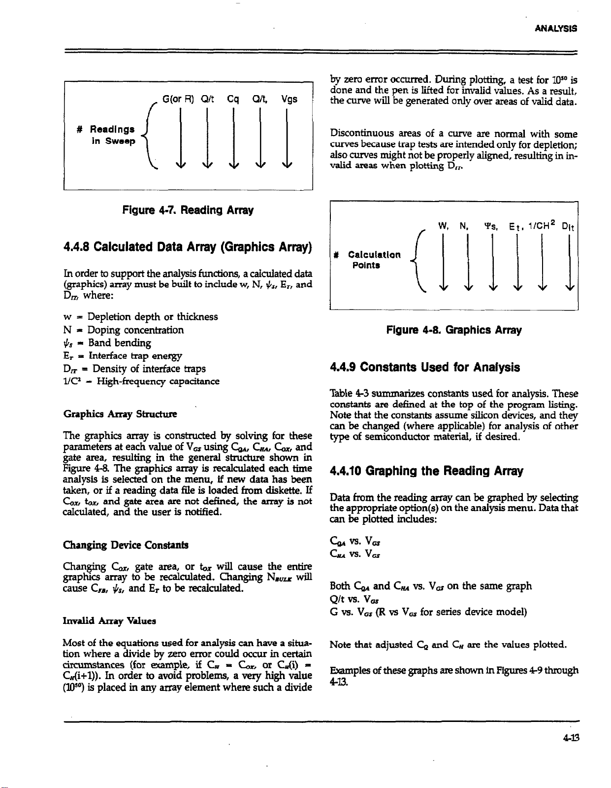
/ G&w R) Q/t Cq Q/t, Vgs 1
Figure 4-7. Reading Array
A?dALYSls
by rem error occurred. During plotting, a test for loSo is
done and the pen is lifted for invalid values. As a result,
the curve will be generated only over areas of valid data.
Discontinuous areas of a curve are normal with some
curves because trap tests are intended only for depletion;
also curves might not be properly aligned, resulting in in-
valid areas when plotting D,
(IU’iE~lli’i
4.4.8 Calculated Data Array (Graphics Array)
In order to support the analysis functions, a calculated data
(graphics) array must be built to include w, N, +$, En and
DITI where:
w = Depletion depth or thickness
N - Doping concentration
Band bending
$6 -
- Interface trap energy
Es
Density of interface traps
Dm =
l/C? = High-frequency capacitance
Graphics Array Stnuzhm
The graphics array is constructed by solving for these
parameters at each value of V, using C, Cu, &, and
gate area, resulting in the general structure shown in
Figure 443. The graphics array is recalculated each time
analysis is selected on the menu, if new data has been
taken, or if a reading data file is loaded from diskette. If
6x, tax, and gate area are not defined, the array is not
calculated, and the user is notified.
# Calcuiatlan
Points
Figure 4-8, Graphics Array
4.4.9 Constants Used for Analysis
Table 43 su mmarizes constants used for analysis. These
constants are defined at the top of the program listing.
Note that the constants assume silicon devices, and they
can be changed (where applicable) for analysis of other
type of semiconductor material, if desired.
4.4.10 Graphing the Reading Array
Data from the reading array can be graphed by selecting
the appropriate option(s) on the analysis menu. Data that
can be plotted includes:
Changing Device Constants
Changing C& gate area, or & will cause the entire
gyp:; array to be recalculated. Changing N,, will
s, and Er to be recalculated.
FBJ
1L
Invalid Array Values
Most of the equations used for anaIysis can have a situa-
tion where a divide by zero error could occur in certain
cimunstances (for example, if C, - & or C&) C&+1)). In order to avoid probIems, a very high value
(Wo) is placed in any array element where such a divide
6.4 vs. VGS
cuvs.vGs
Both C, and CHA vs. Vu on the same graph
Q/t vs. V,
G vs. V,, (R vs V, for series device model)
Note that adjusted C, and CM are the vafues plotted.
Examples of these graphs am shown inFiis 49 thmugh
443.
Page 84

ANALYSIS
.
The curve data represents the low-frequency capacitake of the device under test including interface trap and inversion layer capacitance
.
*a3 / kg
. .
Ffgure 4-9. Quasistatic Capacitance vs. Gate Voltage Example (Normalized to C,)
Page 85

ANALYSIS
f
*
The curva data shows the high-frequency capacitance of the device under test. Interface traps and the inversion layer respond to
the DC bias voltage, but do not follow the high-frequency AC test signal, resulting in reduced capacitance in inversion.
QI
co l-0
.
.
rn cu
.
.
Figure 440. Htgbfrequency vs. Gate Voltage Example (Normalized to C,)
4-15
Page 86

ANALYSIS
w
Y
E
Curve differences result from such phenomena as interface charge trapping or inversion layer formation. Curve alignment errors caused
by voltage stress, mobile ionic charge, and interface trap stretchout are minimized by simultaneous CV measurement.
Figure 441. High-Frequency and Quasistatic vs. Gate Voltage Example
416
Page 87

ANALYSIS
l
”
CM vs. V, data provides an important method of ensuring that the device remains in equilibrium throughout the sweep The curve
shown demonstrates how the current flowing through the DUT rises sharply in inversion IVz =
-2.2V). a sign of nonequilibrium.
Figure 4-12. Q/t vs. Gate Voltage Example
417
Page 88
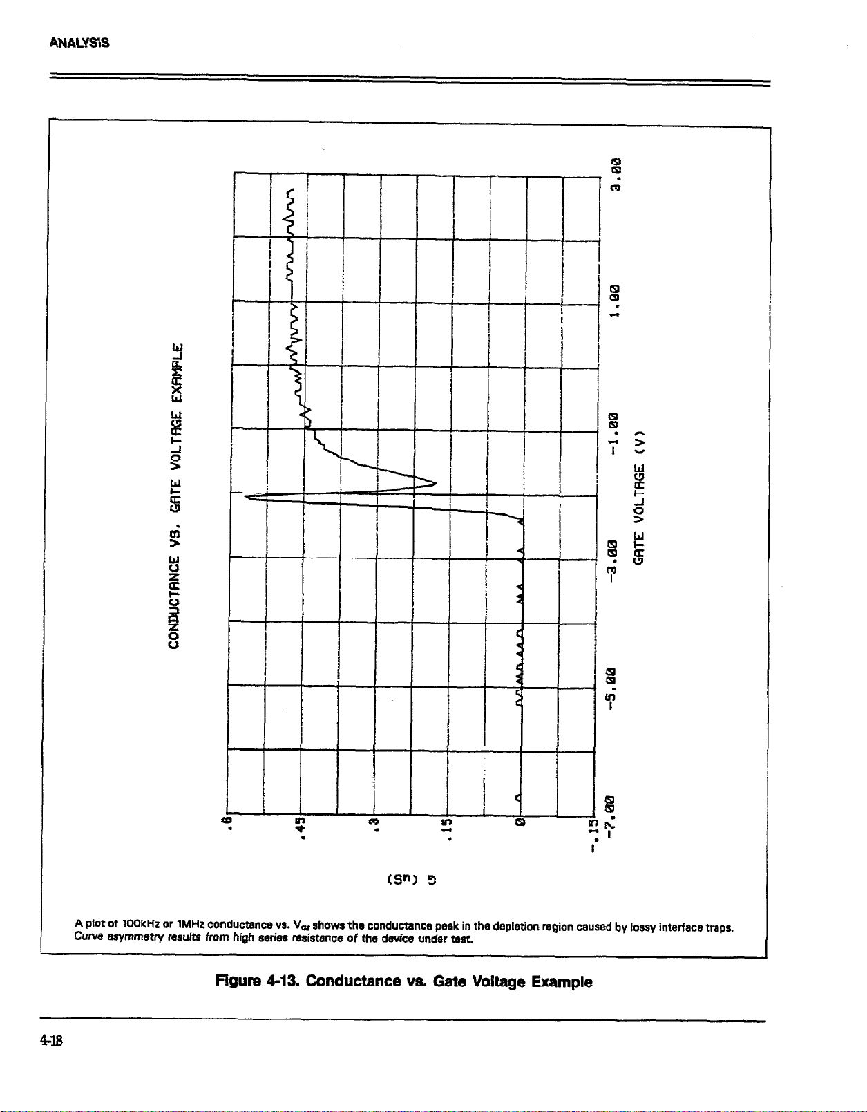
A plot of 1OOkHz or 1MHz conductance vs. VW shows the conductance peak in the depletion region caused by lossy interface traps.
Curve asymmetry results from high series resistance of the device under test.
Figure 4-13. Conductance vs. Gate Voltage Example
Page 89

Table 4-3. Analysis Constants
ANALYSIS
Symbol
lz
eox
z
nI
Description
Charge on an electron
Thermal energy at room
temperature
Permittivity of SiOs
Permittivity of silicon
Energy gap of silicon
Intrinsic carrier concentration
4.4.11. Doping Profile
Doping profile anaiysis includes graphing of depletion
de
vs. gate vohage, doping concentration vs. depth, and
P
I/
a vs. gate voltage, as discussed below.
n-i.d- n-41. ._ ~~~ \~~~gc pN ‘;“p. vGs)
ust.“SU”~’ usyu, *a.
The Package 82 computes the depletion depth, w, from the
high-frequency capacitance and oxide capacitance at each
measured value of V,, (Nicollian and Brews 386).
Depletion depth vs. gate voltage can be graphed by selecting the corresponding option on the analysis menu. Jir
order to graph this function, the program computes each
element of the w column of the calculated data array as
shown below.
Value
1.60219 x lo-I9 Cod
4.046 x lo-y
34 x XYFlcm
1:04 x lO-‘* F/cm
1.l2eV
1.45 x 1010 cm’3
In order to correct for errors caused by interface traps, the
error term (1-Q&)/(1-G/C& is included in the caiculations as follows:
N I (-2x10⁷ [(l-cQKox)1(1-GKox)1
A%@(i)
Where: N = doping concentration (cnP)
C, - quasistatic capacitance (pF)
Gx = oxide capacitance (pF)
C, = high-frequency capacitance (pF)
A - gate area (cml)
q - electron charge (1.60219 x 1P9C)
es = permittivity of silicon (1.04 x I.CP~F/cm)
1 x 10-” = units conversion factor
Where: w = depth &n)
es = permittivity of silicon (1.04 x XPFkm)
- high-frequency capacitance (pF)
CIf
6x - oxide capacitance (pF)
A = gate area (cm’)
Figure 414 shows a typical example of a w vs. Vos plot.
The CV curves for the device are shown in Figure 4-11.
Doping Concentration vs. Depth (N VR w)
The doping profile of the device is derived from the CV
curve based on the definition of the differential capacitance
(measured by the Models 590 and 595) as the differential
change in depletion region charge produced by a diffemntial change in gate voltage (Nicollian and Brews 380489).
And:
A(i) =
Fii 445 shows an example of a N vs. w graph. Figure
4ll shows the CV curves of the DUT.
%?(i+l) - l/C$(i) = A(lK2)
V&i+l) - V&i)
AVGS
A l/C graph can yield important information about dop
ing profile. N is related to the reciprocal of the slope of
*the ‘l/C vs. Vor curve, and the V interce
to the f&band v&age caused by surface
semiconductor work function (NicoBian and Brews 385).
Fii 4-16 shows a typical l/P vs. VGS plot. Data for the
plot is shown in Fiie 421.
point is equal
cf
atge and metal-
419
Page 90

ANALYSIS
?
- s
Y
This curve demonstrates the formation of the depletion region at the onset of depletion, as well as its saturation at maximum depth
at the point where the inversion layer forms.
Figure 4-14. Depth vs. Gate Voltage Example
420
Page 91

ANALYSIS
.
f
.
The doping profile curve shows how the ionized purity density varies as a function of the depletion depth. Doping profile is calculated
from both quasistatic and high-frequency capacitance in order to minimize errors caused by interface states.
Figure 4-15. Doping Prwafile vs. Depth Example
4-n
Page 92

ANALYSIS
The shape of the
is proportional to
422
curve is related to the doping profile in an MOS capacitor. The reciprocal of the slope of the curve
the doping profila
Figure 4-16. 1/Ch2 vs. Gate Voltage Example
at point
Page 93

ANALYSlS
4.4.12 Flatband Capacitance
The Package 82 uses the flatband capacitance method of
finding flatband voltage, V,, . The Debye len@h is used
to calculate the ideal value of fIatband capacitance, C,B .
Once the value of CrB is known, the value of V, is interpolated from the closest Vos values (NicoEian and Brews
487488).
The method used is invalid when interface trap density
becomes very large (W-W and greater). However, this
algorithm should give satisfactory results for most users.
Those who are dealing with high values of D* should consult the appropriate literature for a more appmpriate
method and modify the Package 82 software accordingly.
Based on doping, the calcuIation of C& uses N at 90%
w, or user-supplied NA (bulk doping for p-type, acceptors) or ND (bulk doping for n-type, donors).
C, is calculated as follows:
C
ia = (1x1O-“)(Gx)+~~ Al(l~ltI+)(L~)
Cm es Al(lxW)(Ln)
Analysis Constants” in the menu. Note that changing N
forces a recalculation of $, E, and C,.
4.4.13 Interface Trap Density Analysis
Interface trap density graphical analysis tools in&de interface trap density vs. energy, band bending vs. voltage,
as well both quasistatic and high-frequency capacitance vs.
band bending. In addition, flatband voltage, which is
necessary to determine band bending, is also calculated
as part of the analysis operation.
The CV curve is transformed into a Dm vs. Er curve
(Nicollian and Brews 319-325; Sze 579390). This transfor-
mation is performed using the model shown in Sze (381)
or Nicollian and Brews (Figure 8.1 and 8.3). The interface
capacitance, G, is the only element not in common be-
tween Figures 8.1 and 8.3 (Nicollian and Brews). Howeva,
by measuring both quasistatic and high-frequency
capacitance, we can calculate its value, as discussed below.
Band Bending vs. Gate Voltage (I/x~ vs. V,,)
As a preliminary step, surface potential ($I~ - &) vs. Vos
is calculated with the results placed in the Jls cohunn of
the array. Surface potential is calculated as follows:
where: CF.
And: b L, = extrinsic Debye length -
Where: kT = thermal energy at room temperature (4.046
N at 90% wU is chosen to represent bulk doping.
To change the vaIue of N to N,, or ND, select ‘Display
= flatband capacitance (pF)
& = oxide capacitance (pF)
es - permittivity of silicon (1.04 x lITLIFlcm)
A = gate area (an’)
1 x 10-’ = units conversion for L,
1 x lP2 = units conversion for 6x
cskT
(1 x W) -
x 10-y)
q = electron charge (1.60219 x l@“C)
Nx -
the user.
J
qaNx
N at 90% wW or N,, or ND when input by
Where: (+&) = surface potential (V)
C, = quasistatic capacitance (pF)
Gx = oxide capacitance (pF)
V
= step voltage (V)
STEP
V 0s - gate-substrate voltage (V)
Note that the (h- $) value is accumulated as the column
is built, from the first row of the array (V,, #l) to the last
array row (V, last). The number of mws will, of course,
depend on the number of readings in the sweep, which
is determined by the Start, Stop and Step voltages.
Once (&- $,,) values are stored in the array, the value of
(#s- $,,) at the fI atband voltage is used as a reference point
and is set zero by subtracting that value from each entry
in the (&- &) column, changing each element in the column to $s. The value of & is interpolated as discussed
below.
423
Page 94

ANALYSIS
Once band bending voltage is known, graphs of & vs. V,
C, vs. &, and C, vs & can be generated. Examples are
shown in Figures 417 through 419. Again, CV curves for
the device are shown in Figure 411.
V,, and & Interpolation
The program determines flatband voltage, V, , by locating
the IT,, point where C,, approximately equals CFn . V,, is
then interpolated from the closest V,, values.
A straight line interpolation from the previous or following data points is used, and the interpolated V,, and $,,
points are computed.
Interface Trap Density vs. Energy from Midgap (I& vs Ed
Interface trap density is calculated from Cm as shown
below (Nicollian and Brews 322).
1
err =
WQ - wx) 1 (UC, - Kox)
6x = oxide capacitance (pF)
A = gate area (cn?)
q = electron charge (1.60219 x lo-19C)
1x10-” = units conversion for Clr
The results are stored in the Drr column of the array as
calculated.
Interface trap energy from midgap, E, is computed from
& offset by bulk potential, t#~# as follows:
$s - 6. -Er
Were: & - band bending (V)
interface trap energy from midgap (ev)
Er -
And:
And:
Dm -
Where: Crr = interface trap capacitance (pF)
(1 x lo-‘,) cm
4
Drr - interface trap density (cnP eV’*)
C, = quasistatic capacitance (pF)
high-frequency capacitance (pF)
cff =
Where: t$, = bulk potential (ev)
kT = thermal energy at mom temperature (4.046
x 10-J)
9 - intrinsic carrier concentration in silicon (1.45
x lo’“cm-3)
N at 90% w= , or NA or ND if entered by
Nx =
the user
A typical example of a Dfl vs. E1 plot is shown in Figure
420.
424
Page 95

ANALYSIS
The $I# vs. V, curve aids in understanding how changes in bias voltage affect tha device under test. The accumulation, depletion,
and inversion regions of a CV curve are defined by three specific values of band bending voltage: zero (flatbands), equal to the bulk
potential, and twice the bulk potential IV~-UJ.
Figure 447. Band Bending vs. Gate Voltage Example
425
Page 96

ANALYSIS
.
!i
t
.
P
Y
E
.
9
I
The CQ vs. 4~ curve aids in compering Package 82 curves with previously-teken, manually-eiigned cur&.
Figure 448. Quasistatlc Capacitance vs. Band Bending Example
426
Page 97

ANALYSIS
The C, vs. $= cuwe also aids in comparing to previously taken data.
Flguna 4-19. High-Frequency Capacitance vs. Band Bending Example
42?
Page 98
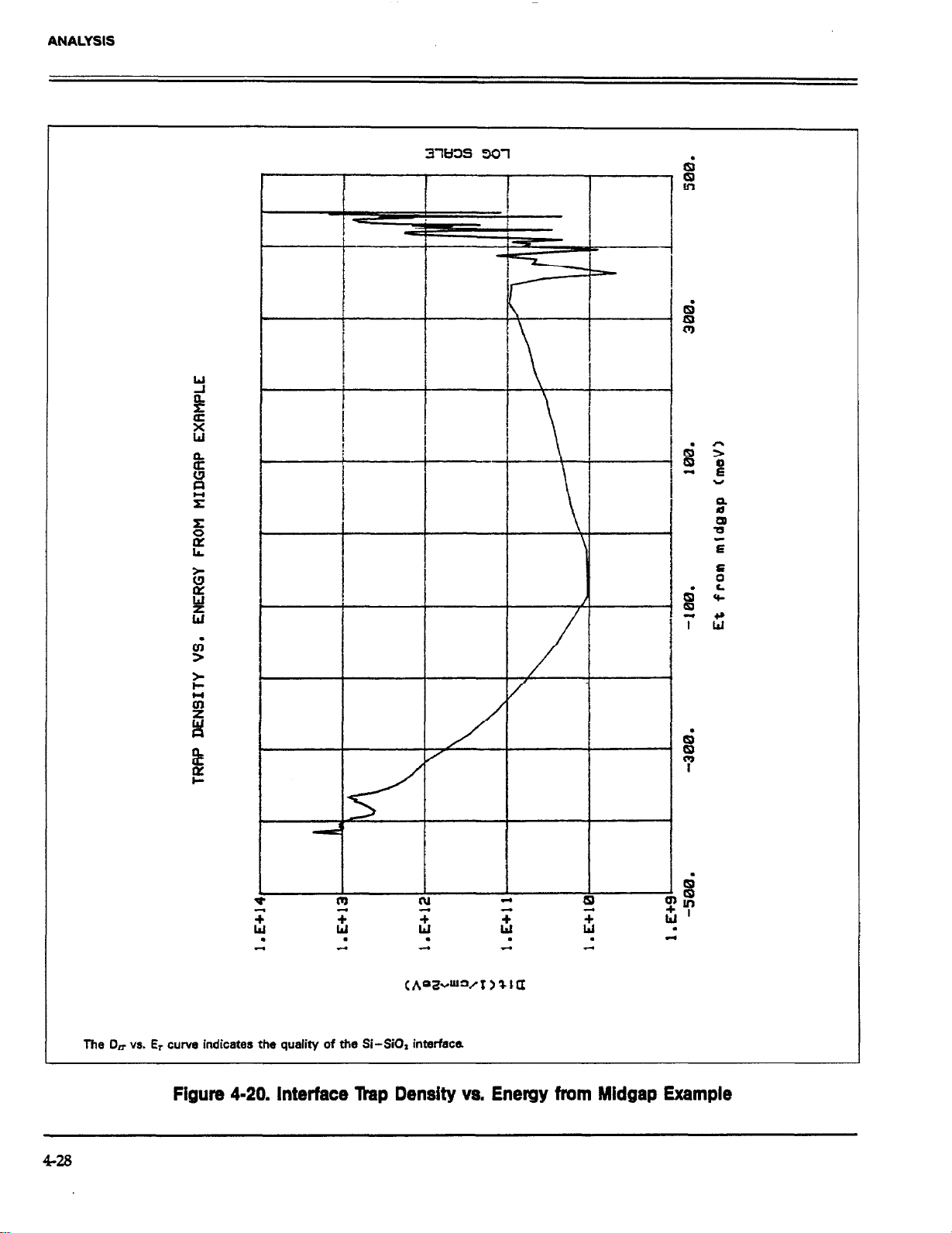
ANALYSIS
The Dm vs. Et curve indicates the quality of the Si-SiOz interfaca
Figure 4-20. Interface lkap Density vs. Energy from Midgap Example
428
Page 99

ANALYSIS
4.4.14 Cakulated Accuracy of N and Dm
The calculated values of N and DR have a nominal error
of < *5% when the depletion depth, w , falls within the
following limits:
Where: LB - extrinsic Debye length (see above)
w = depletion depth (crm)
Nat90%ww,,N,,,orND
Nx =
= intrinsic carrier concentration (1.45 x
nr
3O’%ll-3)
This accuracy range is displayed as best depth under option 4, Display Analysis Constants under the analysis
menu.
NOTE
In order to set the graphics window to the range
of best depth, select option 3 on the analysis menu
followed by option 5 on the subsequent menu.
Type in window limits equal to displayed best
depth. Reading numbers for best depth are shown
in the graphics range selection menu.
Procedure
1. Using the Package 82 or the separate Model 590 program, measure a high-frequency CV curve of the device
at room temperature.
2. Note the flatband voltage, VF, , as calculated and
displayed by the program (select Display Analysis Constants on the analysis menu).
3. Raise the temperature of the DUT to 200~300°C, and
apply a bias voltage of XI-2W for 3-10 minutes.
4. Return the device to room temperature and remove the
bias voltage.
5. Measure a second CV curve of the device at room
temperature.
6. Display the flatband voltage by selecting the Display
Analysis Constants on the analysis menu.
7. Subtract value of V, obtained in step 6 from the value
in step 2 to determine AV, .
Calculation
From NicoBian and Brews (426, Eq. Il.9 and lO.lO), we
have:
4.5 MOBILE IONIC CHARGE CONCENTRATION
MEASUREMENT
Mobile ionic charge concentration in the oxide of an MOS
device must be carefully controlled during the manufacturing process. Sodium ion concentrations are particular-
ly important because of their abundance in the environment and the fact that they move rapidly through the
oxide.
The following paragraphs discuss two methods for
measuring mobile ionic charges in the tide: the flatband
voltage shift method, and the triangular voltage sweep
(TVS) method.
4.51 Flatband Voltage Shift Method
The primary method for measuring oxide charge density
is the flatband voltage shift or temperature-bias stress
method (Snow et al). In this case, two high-frequency CV
curves are measured, both at room temperature. Between
the two curves, the device is biased with a v&age at
2#-WC to drift mobile ions across the oxide. The flat-
band voltage differential between the two curves is then
calculated, from which charge density can be determined.
where: -a&
For the common case of thermally-grown oxide,
T(before)- ~0 and -j?(after)pO, so that
AV, = +
= the first moment of the charge distribution
X = charge centroid
w&c* =
(constant)
ear = oxide dielectric constant
~0 - oxide thickness
& = oxide capacitance
metal semiconductor work function
X
429
Page 100

ANALYSIS
where QO is the effective charge. Divide QO by the gate area
to obtain mobile ion charge density per unit area.
4.52 Triangular Voltage Sweep Method
A second but Iess familiar way to measure oxide charge
density is the triangular voltage sweep (TVS) method
(Nicollian and Brews 435-440). There are four key advantages of the TVS method over the CV method including:
1. Mobile ion density measurements are accurate even in
cases where interface trap density levels vary
substantially.
2. Different mobile ion species such as sodium and
potassium can be distinguished from one another.
3. Greater sensitivity allowing low ion densities to be
detected.
4. Greater speed because only one curve is required, in
addition to the fact that the device can remain heated
for several measurements.
Procedure
1. Load the “M595CV” program into the computer.
2. Connect the Model 595 to the test fixture containing the
device under test.
3. Raise the temperature of the device to a.temperature of
300°C and maintain the DUT at that temperature
throughout the test.
4. Perform a quasistatic measurement by sweeping from
-V,, to +Vos at the required amplitudes. Keep in mind
that Step V must be low enough and T delay must be
long enough so that G I & in the absence of mobile
ions.
5. Display or print out the reading array to obtain the C,
and V, values. Calculations can be performed as outlined below.
+VCiS
I- (c,, - C,)AV,, = qNN
xvos) Y(-Vos)
- --
1
Lx, XOJ
-E
Where:
or, for the case of thermally-grown oxide, the above reduces
to:
+v,
-v,,
Proof of Measurement Method
An adaptation of the proof by Nicollian and Brews (437)
follows. This pmof describes the validity of the feedback
charge technique as applied to the TVS method for
measuring oxide charge density,
Objective:
To demonstrate that mobile ion density drift at a given
temperature is proportional to the area under the peak in
a quasistatic CV curve caused by ionic motion as shown
below.
V
= gate-substrate voltage
AyGs = change in gate substrate voltage (V step)
c-=
Ck = oxide capacitance
q - ekctron &arge
NM = mobile ion density
?? - charge centroid
~0 = oxide thickness
Q. = mobile ion charge
(c- - 6x) AV, = - Qo
c
quasistatic capacitance measured by 595
Calculations
Although the method presented here was originally
developed for the ramp technique of quasistatic measurement, the Model 595 is used to make the necessary
measurement. The end result is the same: the area
between the measured capacitance curve and & indicates
the charge density as shown.
Assumptions:
1. Temperature is high enough ( a 300°C) and the staircase
is slow enough ( ~lOOmV/sec) so that C, =e Car in the
absence of mobile ions.
2. AV, is in the small signal range.
Model:
The model for the derivation of pmof is shown in Figure
421.
 Loading...