

Page 1

P7630
xx
ZZZ
TriMode™ Probe
Technical Reference
*P077068001*
077-0680-01
Page 2

Page 3

xx
P7630
ZZZ
TriMode™ Probe
Technical Reference
www.tektronix.com
077-0680-01
Page 4

Copyright © Tektronix. All rights reserved. Licensed software products are owned by Tektronix or its subsidiaries
or suppliers, and are protected by national copyright laws and international treaty provisions.
Tektronix products are covered by U.S. and foreign patents, issued and pending. Information in this publication
supersedes that in all previously published material. Specifications and price change privileges reserved.
TEKTRONIX and TEK are registered trademarks of Tektronix, Inc.
TriMode is a trademark of Tektronix, Inc.
Velcro is a registered trademark of Velcro Industries B.V.
G3PO is a trademark of Corning Gilbert Inc.
Contacting Tektronix
Tekt roni
14150 SW Karl Braun Drive
P.O . Bo x 5 0 0
Beaverton, OR 97077
USA
For pro
x, Inc.
duct information, sales, service, and technical support:
In North America, call 1-800-833-9200.
Worldw i d e , visit www.tektronix.com to find contacts in your area.
Page 5

Warranty
Tektronix warrants that this product will be free from defects in materials and workmanship for a period of one (1)
year from the date of shipment. If any such product proves defective during this warranty period, Tektronix, at its
option, either will repair the defective product without charge for parts and labor, or will provide a replacement
in exchange for the defective product. Parts, modules and replacement products used by Tektronix for warranty
work may be n
the property of Tektronix.
ew or reconditioned to like new performance. All replaced parts, modules and products become
In order to o
the warranty period and make suitable arrangements for the performance of service. Customer shall be responsible
for packaging and shipping the defective product to the service center designated by Tektronix, with shipping
charges prepaid. Tektronix shall pay for the return of the product to Customer if the shipment is to a location w ithin
the country in which the Tektronix service center is located. Customer shall be responsible for paying all shipping
charges, duties, taxes, and any other charges for products returned to any other locations.
This warranty shall not apply to any defect, failure or damage caused by improper use or improper or inadequate
maintenance and care. Tektronix shall not be obligated to furnish service under this warranty a) to repair damage
result
b) to repair damage resulting from improper use or connection to incompatible equipment; c) to repair any damage
or malfunction caused by the use of non-Tektronix supplies; or d) to service a product that has been modified or
integrated with other products when the effect of such modification or integration increases the time or difficulty
of servicing the product.
THIS WARRANTY IS GIVEN BY TEKTRONIX WITH RESPECT TO THE PRODUCT IN LIEU OF ANY
OTHER WARRANTIES, EXPRESS OR IMPLIED. TEKTRONIX AND ITS VENDORS DISCLAIM ANY
IMPLIED WARRANTIES OF MERCHANTABILITY OR FITNESS FOR A PARTICULAR PURPOSE.
TRONIX' RESPONSIBILITY TO REPAIR OR REPLACE DEFECTIVE PRODUCTS IS THE SOLE
TEK
AND EXCLUSIVE REMEDY PROVIDED TO THE CUSTOMER FOR BREACH OF THIS WARRANTY.
TEKTRONIX AND ITS VENDORS WILL NOT BE LIABLE FOR ANY INDIRECT, SPECIAL, INCIDENTAL,
OR CONSEQUENTIAL DAMAGES IRRESPECTIVE OF WHETHER TEKTRONIX OR THE VENDOR HAS
ADVANCE NOTICE OF THE POSSIBILITY OF SUCH DAMAGES.
[W2 – 15AUG04]
btain service under this warranty, Customer must notify Tektronix of the defect before the expiration of
ing from attempts by personnel other than Tektronix representatives to install, repair or service the product;
Page 6

Page 7

Table of Contents
General safety summary ........ ................................ .................................. ................ iv
Preface ............................................................................................................. vii
Theory of Operation....................... ................................ ................................ ......... 1
Introducti
TriMode Operation ....... .................................. ................................ ................... 6
Operating Voltages............................................................................................. 8
Input Impedance and Probe Loading ....... ................................ ................................ 14
Scale Factor ................................................................................................... 16
Probing Techniques to Maximize Measurement Fidelity . . ... . ... . ... . . ... . ... . ... . ... . ... . ... . ... . ... . . 17
Referen
Single-Ended Measurements Using A and B Modes ......... ................................ ............ 23
Differential Measurements................................................................................... 24
Specifications ................................ ................................ .................................. .... 27
Warranted Characteristics.................................................................................... 27
Typical Characteristics ............. ................................ ................................ .......... 30
Nomi
User Service ........................................................................................................ 35
Error Condition . . ... . ... . ... . ... . ... . ... . ... . ... . ... . ... . ... . ... . ... . ... . ... . ... . ... . ... . ... . ... . .. . . .. . . .. . . . 35
Replaceable Parts ............................................................................................. 35
Preparation for Shipment .............. ................................ ................................ ...... 40
Index
on.............................. ................................ ................................ ....... 1
ce ........................................................................................................... 23
nal Characteristics...................................................................................... 34
P7630 TriMode Probe Technical Reference i
Page 8

Table of Contents
List of Figure
Figure 1: Adapters for the P7630 probe.......................................................................... 3
Figure 2: Pr
Figure 3: TriMode input structure ................................................................................ 7
Figure 4: Typical TriMode Probe Setup screen ......... ................................ ....................... 7
Figure 5: Probe inputs ........................ ................................ ................................ ..... 8
Figure 6: Operating voltage window ............................................................................ 9
Figure 7: Dynamic range versus linearity .......................... ................................ ............ 10
Figure 8:
Figure 9: Probe Setup screen..................................................................................... 12
Figure 10: TriMode probe coaxial input model.... ................................ ............................ 14
Figure 11: P76TA adapter simplified schematic ............................................................... 15
Figure 12: P76TA adapter and P75PST tip equivalent schematic........................ .................... 15
Figure 13: Preventing twist to the coaxial input cables ................... ................................ .... 17
Figur
Figure 15: Solder ramp installed......................... .................................. ...................... 18
Figure 16: Typical wire length from probe tip to circuit ...................................................... 20
Figure 17: P75TLRST solder tip with 0.010 in. of tip wire .................................................. 21
Figure 18: P75TLRST solder tip with 0.050 in. of tip wire .................................................. 21
Figure 19: P75TLRST solder tip with 0.100 in. of tip wire .................................................. 22
gure 20: P75TLRST solder tip with 0.200 in. of tip wire .................................................. 22
Fi
Figure 21: Simplified model of a differential amplifier ....................................................... 24
Figure 22: Typical CMRR ... .................................. ................................ .................. 25
Figure 23: Typical channel isolation ............................................................................ 26
Figure 24: Typical rise time ...................................................................................... 31
Figure 25: Typical frequency response.......................... ................................ ................ 31
Figure 26: Probe body and control box dimensions........................................................... 32
Figure 27: P7630 Probe adapter dimensions .................... .................................. ............ 33
Figure 28: P75PST and P75TLRST solder tip dimensions................................................... 33
Figure 29: Removing the bullets................................................................................. 36
Figure 30: Installing the bullets. . . ... . ... . ... . ... . ... . ... . ... . ... . ... . ... . ... . ... . ... . . .. . . .. . . .. . . .. . . ... . ... . .. 37
obe Tip Selection screen.............................. .................................. ............. 4
Termination voltage operating range ...................... ................................ .......... 11
e 14: P75PST and P75TLRST TriMode Solder Tips.............................. ...................... 18
s
ii P7630 TriMode Probe Technical Reference
Page 9

List of Tables
Table 1: Offset ranges....... ................................ .................................. .................... 23
Tabl e 2: War
Table 3: Warranted environmental characteristics..... ................................ ........................ 29
Table 4: Typical electrical characteristics................. .................................. .................... 30
Table 5: Typical mechanical characteristics .................................................................... 30
Table 6: Nominal electrical characteristics ....... ................................ .............................. 34
Table 7: Nominal adapter electrical characteristics.................. ................................ .......... 34
Tabl e 8: T
Table 9: Required equipment..................... ................................ ................................ 35
ranted electrical characteristics . ................................ ................................ .. 27
riMode probes replaceable parts ....................... ................................ .............. 35
Table of Contents
P7630 TriMode Probe Technical Reference iii
Page 10

General safety summary
General safet
To avoid fire or personal
injury
ysummary
Review the fo
this product or any products connected to it.
To avoid pot
Only qualified personnel should perform service procedures.
While using this product, you may need to access other parts of a larger system.
Read the safety sections of the other component manuals for warnings and
cautions r
Connect and disconnect properly. Connect the probe output to the measurement
instrument before connecting the probe to the circuit under test. Connect the
probe reference lead to the circuit under test before connecting the probe input.
Disconnect the probe input and the probe reference lead from the circuit under test
before
Observe all terminal ratings. To avoid fire or shock hazard, observe all ratings
and ma
information before making connections to the product.
Do no
exceeds the maximum rating of that terminal.
disconnecting the probe from the measurement instrument.
t apply a potential to any terminal, including the common terminal, that
llowing safety precautions to avoid injury and prevent damage to
ential hazards, use this product only as specified.
elated to operating the system.
rkings on the product. Consult the product manual for further ratings
ot operate without covers. Do not operate this product with covers or panels
Do n
removed.
ot operate with suspected failures. If you suspect that there is damage to this
Do n
product, have it inspected by qualified service personnel.
oid exposed circuitry. Do not touch exposed connections and components when
Av
power is present.
o not operate in wet/damp conditions.
D
Do not operate in an explosive atmosphere.
Keep product surfaces clean and dry.
iv P7630 TriMode Probe Technical Reference
Page 11

General safety summary
Terms in this manual
Symbols and terms on the
product
These terms may
WAR NING . Warning statements identify conditions or practices that could result
in injury or loss of life.
CAUTION. Caution statements identify conditions or practices that could result in
damage to this product or other property.
These terms may appear on the product:
DANGER in
the marking.
WAR NI NG
read the marking.
CAUTIO
The following symbol(s) may appear on the product:
appear in this manual:
dicates an injury hazard immediately accessible as you read
indicates an injury hazard not immediately accessible as you
N indicates a hazard to property including the product.
P7630 TriMode Probe Technical Reference v
Page 12

General safety summary
vi P7630 TriMode Probe Technical Reference
Page 13

Preface
This manual discusses topics that are not covered in depth in the P7630 TriMode
Probe Quick Start User Manual.
The main sections are:
Theory of Operation — Contains probe details not covered in the user manual.
Reference — Contains information about differential m easurements and how
to increase measurement accuracy.
Specifications — Contains warranted, typical, and nominal characteristics for
the probe, probe adapters and probe tip accessories.
User Service — Describes troubleshooting and probe maintenance.
P7630 TriMode Probe Technical Reference vii
Page 14

Preface
viii P7630 TriMode Probe Technical Reference
Page 15

Theory of Operation
This section discusses operating considerations and probing techniques. For more
detailed information a bout differential measurements and TriMode operation,
refer to Refe
Introduction
rence. (Seepage23.)
Probe Components
The P7630 T
and DPO73304D oscilloscopes. These oscilloscope models feature an
extended-bandwidth version of the TekConnect probe interface designed to
support bandwidths up to 33 GHz. The P7630 probes contain probe-specific
S-parameter data that, when transferred to the host oscilloscope after the initial
connection is made, create unique system DSP filters.
The P7630 TriMode probe is optimized for high bandwidth; it is not a
general-purpose probe. The P7500 Series probe solder tips that can be used
with th
circuitry, and must be handled carefully.
The P7630 probe is comprised of a control box, an active probe head, and an
connect cable that transfers measured signals, power, and control signals
inter
between the control box and probe head. An optional adapter is required on the
probe head to make the final connection to the DUT (device under test).
Control box. The P7630 probe control box assembly mates to the host instrument
through an extended-bandwidth, 33 GHz TekConnect probe interface. The control
includes a membrane toggle switch to select the TriMode input mode:
box
Differential (A–B)
riMode probe is a 30 GHz probe designed for use with DPO72504D
e probe are m iniaturized for electrical characteristics and a ccess to dense
A input (single-ended to ground)
B input (single-ended to ground)
Common-mode (A+B/2 to ground)
The probe input mode can also be selected using the host oscilloscope Probe
Control menu.
LEDs on the control box front and top panels indicate the selected input mode.
Another LED on each panel indicates when an overload condition exists.
Overloads are caused when parameters such as input voltages or termination
voltage driver currents exceed the safe limits of the probe.
P7630 TriMode Probe Technical Reference 1
Page 16

Theory of Operation
A mechanical la
instrument during use. The thumbscrew is only intended to be finger-tightened,
and is machined to prevent tools from being used to over-torque it. To remove
the probe, loosen the thumbscrew counterclockwise, depress the latch button to
release the probe, and then pull out the probe.
CAUTION. To prevent damage to the probe, use care when handling the probe.
Rough or car
Interconnect cable. This cable consists of a low-loss coaxial signal cable that
carries t
includes a 20-conductor bundle of wires that supply probe head power and control
signals from the control box. Some of the wires carry bidirectional data, such as
queries and responses about the type of probe adapter that is attached to the probe
head, and other probe-specific information.
Probe h
and other support circuitry that precondition the acquired signals. It connects to
the optional coaxial and solder tip adapters through a connector that, like the
interconnect cable, carry signal, control and power signals.
The P7630 probe head is intended to be placed close to the DUT test point,
within the final few inches (6 inches or less, for best performance), made with the
optional coaxial and solder tip adapters.
he acquired signal from the probe head to the control box. The cable also
ead. The probe head is an active component that houses an amplifier
tch and retention thumbscrew hold the probe securely to the
eless use can damage the probe.
pters. The P7630 probe requires optional TriMode adapters to complete the
Ada
connection between the probe and your circuit. (See Figure 1 on page 3.) The
adapters connect the P7630 probe to your circuit through 2.92 mm or SMP coaxial
cables. For soldered, in-circuit connections, the connection is made through
P7500 Series solder tips, such as the P75PST Performance Solder Tip.
There are several different coaxial tips available for the probe, which differ only
in the tip connector type or the tip cabling. All of the coaxial tips provide a 50
ohm transmission line signal path from its input connector to the termination
resistor at the probe amplifier input.
The adapter inputs are polarized, with the A input marked in red and the B input
marked in black. All of the adapters are secured to the probe head with a 2 mm
hex screw. Although the adapters can be “hot-plugged” (with the probe connected
to the oscilloscope and powered on), the adapters should first be connected to
the probe before the probe is connected to the instrument. This ensures a good
power-on sequence for both the probe and attached adapter. After the probe
is powered on with an attached adapter, data is transferred from the adapter,
identifying it to the probe and oscilloscope.
2 P7630 TriMode Probe Technical Reference
Page 17

Figure 1: Adapters for the P7630 probe
1. P76CA-292: 2.92 mm Coax Adapter
Theory of Operation
2. P76CA-292C: 2.92 mm Coax Adapter with cables
3. P76CA-S
4. P76TA: P7500 TriMode Solder Tip Adapter (shown with P75PST
Perfor
Use the P76CA-292 adapter with high bandwidth, low skew (<2 ps) cable pairs
ave short (<6 in) lengths and high-quality male 2.92 mm connectors at the
that h
probe end. The other end of the cables can be customized with connectors that
mate to your circuit.
MP: SMP Coax Adapter with cables
mance Solder Tip)
P7630 TriMode Probe Technical Reference 3
Page 18
Theory of Operation
P7500 Series so
soldered connections to the DUT. You must manually choose the solder tip that
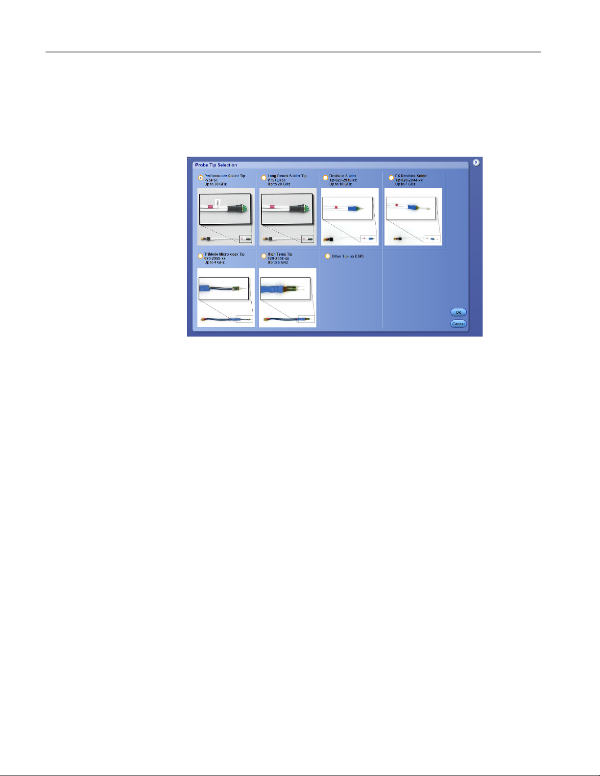
you are using in the Probe Tip Selection screen. (See Figure 2.) This enables the
correct DSP filtering to be used for your measurements. Maximum probe solder
tip performance is only provided by the P75PST Performance Solder Tip.
Figure 2
: Probe Tip Selection screen
lder tips. These tips are used with the P76TA adapter to make
4 P7630 TriMode Probe Technical Reference
Page 19

Theory of Operation
Probe Input Architecture
The input struc
tip versions, and are discussed below.
Coaxial Adapters. When a P76CA-xxx coaxial adapter is attached to the P7630
probe, it provides a low VSWR, 50 ohm terminated input for taking TriMode
differential signaling measurements. In order to provide low noise measurement
performanc
attenuation, which results in a relatively low dynamic range limit. The P7630
probe has a quite large Offset Voltage and Termination Voltage adjustment range,
however, which enables optimum placement of the probe dynamic range within
the larger operating voltage window.
Low noise performance is also enhanced in the P7630 probe by the
design of the probe amplifier, which features five step gain settings
(0.25X/0.5X/1.0X/2.0X/4.0X). This step gain control enables lower noise
perform
channel scale factors. The optimum step gain setting is automatically selected by
the host oscilloscope, based on the selected vertical channel scale factor.
Solder Tip Adapter. When a P76TA solder tip adapter and P75PST solder tip
are attached to the P7630 probe, it provides a passive attenuation of the input
signa
structure, which is enhanced by the adjustable termination voltage capability
of the P7630 probe. For the common use case of probing a doubly-terminated
50 ohm transmission line, this results in a 5X broadband attenuation and a 225
ohm loading. (See Figure 12 on page 15.) The signal loss due to this broadband
loading is automatically compensated by boosting the measured signal gain,
as
ance by boosting the signal output amplitude at the more sensitive vertical
l to the probe. This passive attenuation network forms a Z0 probe input
suming a 25 ohm signal source impedance.
ture of the probe adapters differ between the coaxial and solder
e, the coaxial adapters connect the input signal to the probe without
This input attenuation of 5X also expands the single ended dynamic range at the
older tip by the same 5X factor to ±3.0 V. (See Figure 6 on page 9.) The probe
s
noise is also increased by the same 5X factor due to the solder tip attenuation.
CAUTION. To avoid damaging the P75PST and P75TLRST solder tip resistors, do
not allow the termination voltage to differ from either the A or B input voltage by
more than 5 volts. The small size of the solder tip resistors expose them to thermal
damage within the operating conditions of the probe.
P7630 TriMode Probe Technical Reference 5
Page 20

Theory of Operation
TriMode Opera
tion
The TriMode feature of the P7630 probe is designed for improved convenience
and enhanced capability in measuring differential signal quality. Since a
differentia
full characterization of differential signal quality requires more than a simple
differential measurement. A TriMode probe features three Input Modes that allow
a differential signal to be fully characterized with four measurements: differential,
positive polarity and negative polarity single-ended, and common mode.
A TriMode probe provides improved efficiency and convenience by enabling full
differential signal characterization from a pair of coaxial cable connections or a
single soldered connection, depending on the type adapter used.
The P76CA-292C and P76CA-SMP coaxial adapters provide a pair of integral
6-inch coaxial leads with male 2.92 mm or female SMP connectors at the cable
ends. Th
to allow for an off-the-shelf or custom cable connection to the DUT. Coaxial
adapters provide a TriMode signal ground connection through the integral DUT
connector shield connections.
Using a P76TA adapter and one of the P7500 series solder tips available for
the TriMode probes, (for example, the P75PST probe tip), probe connections
are soldered to the two complementary signals (the A signal and the B signal)
and a ground reference. From this single DUT (device under test) connection,
the
of the three probe Input Modes (four measurements) to be selected at a time.
The TriMode probe inputs are routed on the probe ASIC (application-specific
integated circuit) to a set of four independent input amplifiers that perform the
following signal calculations:
l signal is composed o f two complementary single-ended signals,
e P76CA-292 adapter has two female 2.92 mm coaxial connectors
internal electronic switching control of the TriMode probe allows any one
A – B (for differential signal measurement)
A – GND (for positive polarity single-ended measurement)
B – GND (for negative polarity single-ended measurement)
[A+B]/2 - GND (for common mode measurement)
NOTE. In the B – GND Mode, the negative polarity B input is not inverted.
The four input amplifiers are multiplexed together and only the selected Input
Mode function is output to the connected oscilloscope. (See Figure 3 on page 7.)
The figure shows a conceptual view of the TriMode probe input structure, where
the C input provides the probe ground reference and is connected to the probe tip
ground interconnect using the probe tip cable coaxial shields.
6 P7630 TriMode Probe Technical Reference
Page 21

Theory of Operation
Figure 3: TriMode input structure
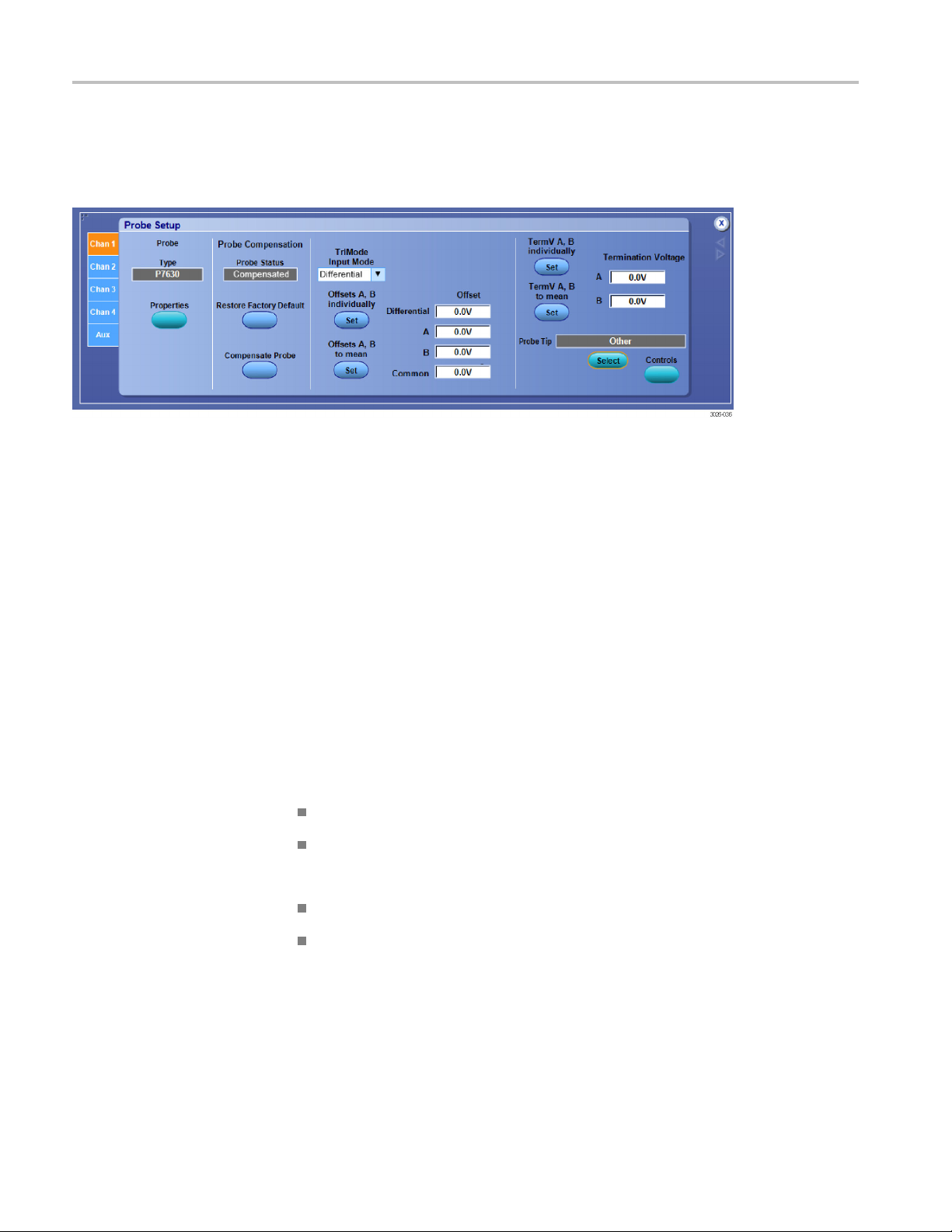
On oscilloscopes that provide full TriMode support, the oscilloscope-controlled
probe G
operation on all Input Modes and Attenuation Settings at once using the Probe
DC Calibration fixture that is supplied with the P7630 probe. (See the P7630
Quick Start User Manual for instructions on running the Probe Cal routine.) Full
TriMode support will also allow storage and automatic recall of relevant settings
like Offset Voltage and Termination Voltage. (See Figure 4.)
Figure 4: Typical TriMode Probe Setup screen
UI (graphical-user interface) can perform a Probe Compensation
P7630 TriMode Probe Technical Reference 7
Page 22

Theory of Operation
Operating Vol
tages
The P7630 TriMode probe is designed to probe low-voltage circuits. Before
probing a circuit, take into account the limits for the operating voltages discussed
in this secti
Input voltage
Operating voltage window
Input signal dynamic range
Offset voltage
Termination voltage
on.
Input
Voltage
Figure 5: Probe inputs
The maximum input voltage is the maximum voltage to ground that the inputs
can withstand without damaging the probe input circuitry. The maximum input
voltage differs between the type of adapter used; the limit for the coaxial adapters
5 V (DC + peak AC). The P76TA solder tip adapter can withstand up to ±8 V
is ±
(DC + peak AC). To avoid damaging the resistors on the P75PST and P75TLRST
solder tips, do not allow the A or B input voltage to differ from the termination
voltage by more than 5 volts. The small size of the solder tip resistors expose
them to thermal damage within the operating conditions of the probe.
CAUTION. To avoid damaging the inputs of the probe, when using the coaxial
dapters, do not apply more than ±5 V (DC + peak AC) between either probe
a
input and ground.
When using the P76TA solder tip adapter, do not apply more than ±8 V (DC +
peak AC) between either probe input and ground.
CAUTION. To avoid ESD damage to the probe, always use an antistatic wrist
strap (provided with your probe), and work at a static-approved workstation when
you handle the probe.
8 P7630 TriMode Probe Technical Reference
Page 23

Theory of Operation
Operating Voltage Window
The operating v
to each input, with respect to earth ground, without saturating the probe input
circuitry. (See Figure 6.) A common-mode voltage that exceeds the operating
voltage window may produce an erroneous output waveform even when the
dynamic range specification is met. The single-ended voltage range (shown as
squares in the figure below) represent the maximum signal swing at the dynamic
range limit
more sensitive on the host oscilloscope.
oltage window defines the maximum voltage that you can apply
s. The squares will shrink in size as the vertical scale factor is made
Figure 6: Operating voltage window
t Signal Dynamic
Inpu
Range
The input signal dynamic range is the maximum voltage difference between the A
and B inputs that the probe can accept without distorting the signal. The distortion
from a voltage that exceeds this maximum can result in a clipped or otherwise
ina
error over the dynamic voltage range of the probe. (See Figure 7.)
Th
as the single-ended signal dynamic range, but this is true only for complementary
A and B input signals. The single-ended A and B dynamic range limits still apply,
even for the case of a maximum differential mode input signal.
ccurate measurement. The graph on the fo llowing p age illustrates the linearity
e differential input mode dynamic range is specified to be almost twice as large
P7630 TriMode Probe Technical Reference 9
Page 24

Theory of Operation
Offset Voltage
The probe A and B
internal circuitry and the sensed values are used by the automatic Offset Voltage
Set control buttons. Two Set control buttons are available; set Individually and
set to Mean.
The Offset Voltage Control, accessible from both the attached oscilloscope
front-panel control and on-screen user interface, allows the probe dynamic range
to be effectively moved up and down within the limits of the offset voltage range
and the operating voltage window. When the offset voltage is set to zero volts and
the input s
signal should be zero volts. If a noticeable zero volt offset is present under the
above conditions, a Probe Compensation operation should be performed. (See the
P7630 Probe Quick Start User Manual).
ignal is zero volts (inputs shorted to ground, not open), the displayed
signal inputs ar e sensed, monitored, and averaged by probe
Figure 7: Dynamic range versus linearity
10 P7630 TriMode Probe Technical Reference
Page 25

Theory of Operation
Termination Voltage
When the probe i
similar to the Tektronix P7313SMA differential probe. Like an SMA-input probe,
the P7630 probe with a coaxial adapter features a user-adjustable termination
voltage, VTERM, which can be controlled independently for both the A and B
probe inputs. Adjustable termination voltage allows greater flexibility than is
possible with the more conventional grounded termination, enabling the user to
minimize DC
The user interface on the oscilloscope allows you to select a preset termination
voltage le
on the A and B inputs. You can also manually enter a value between –4.0 and +
4.0 volts in the on-screen Termination Voltage field.
The diagonal overload limits shown in the figure below are the result of current
limiting the termination voltage drivers to 50 mA. The flat upper and lower input
overload limits are the result of specified voltage limits for the probe amplifier.
vel (mean of both inputs o r independent), based on the voltages sensed
s used with a coaxial tip, i t operates like an SMA-input probe
probe loading from a DUT DC common-mode bias voltage.
Figure 8: Termination voltage operating range
An important limitation of the termination voltage exists when you are using
e P76TA adapter with the P75PST and P75TLRST solder tips. It is possible
th
to damage the solder tips by applying too much voltage to the tips, through a
combination of input and termination voltages.
CAUTION. To prevent exceeding the 62.5 mW power rating of the input resistors
on the solder tips, do not allow the termination voltage to differ from the input
voltage by more than 5 volts.
P7630 TriMode Probe Technical Reference 11
Page 26
Theory of Operation
Autoset of Offset and
Term ination Voltage
Figure 9: Probe Setup screen
You c a n se t b ot h
each input mode. For reference, the TriMode Input Mode field displays the active
input mode in the Offset area of the Probe Setup screen.
Offset Voltage. The offset voltage control sums an adjustable DC voltage with
the probe signal input. It is commonly used to null out an input DC bias voltage
to cente
input. The P7630 A and B probe inputs both have an independent offset voltage
control. Each of the four TriMode input modes also have an independently-stored
pair of offset voltage settings.
r the input signal swing within the linear dynamic range of the probe
the offset and termination voltages to levels that are unique for
Offset voltages may be automatically generated by the probe and can be selected
using the two Set buttons in the Offset section of the Probe Setup screen. You can
also enter specific offset values directly in the Offset fields.
There are four manual Offset Voltage value entry fields which also display the
current Offset Voltage settings. Although all four Offset Voltage value entry fields
are active, only two of the control pairs are independent. The manual controls
eract with each other as follows:
int
Adjusting the A or B settings affects the Differential and Common settings:
Differential = (A – B)
Common = (A + B)/2
Adjusting the Differential or Common settings affects the A and B settings:
A = Common + (Differential/2)
B = Common – (Differential/2)
12 P7630 TriMode Probe Technical Reference
Page 27

Theory of Operation
Termination Vo
voltage which drives the far end of the input termination resistor with a current
limited DC termination voltage. It is generally used to minimize the DC loading
of the probe on the input signal. The P7630 A and B inputs both have an
independent termination voltage control.
Each of the four TriMode input modes also have an independently-stored pair
of termination voltage settings. Termination voltages may be automatically
generated by the probe and can be selected using the two Set buttons in the
Term i nati
values for the A and B inputs directly in the Termination Voltage fields.
In genera
being driven from a relatively low impedance signal source. If the termination
voltage autoset button is activated when either the A or B probe input is open, the
current termination voltage effectively drives the input sense signal used by the
autoset feature. If the termination voltage autoset button is repeatedly actuated
with an open probe input, the termination voltage setting will begin to ramp in the
ion of the accumulated error voltage in the input sense signal path.
direct
ltage. The termination voltage control sets an adjustable DC
on Voltage section of the Probe Setup screen. You can also enter specific
l, the termination voltage autoset feature assumes that the input signal is
P7630 TriMode Probe Technical Reference 13
Page 28

Theory of Operation
Input Impedance and Probe Loading
When you connect the probe inputs to a circuit, you are introducing a new
resistance, capacitance, and inductance into the circuit.
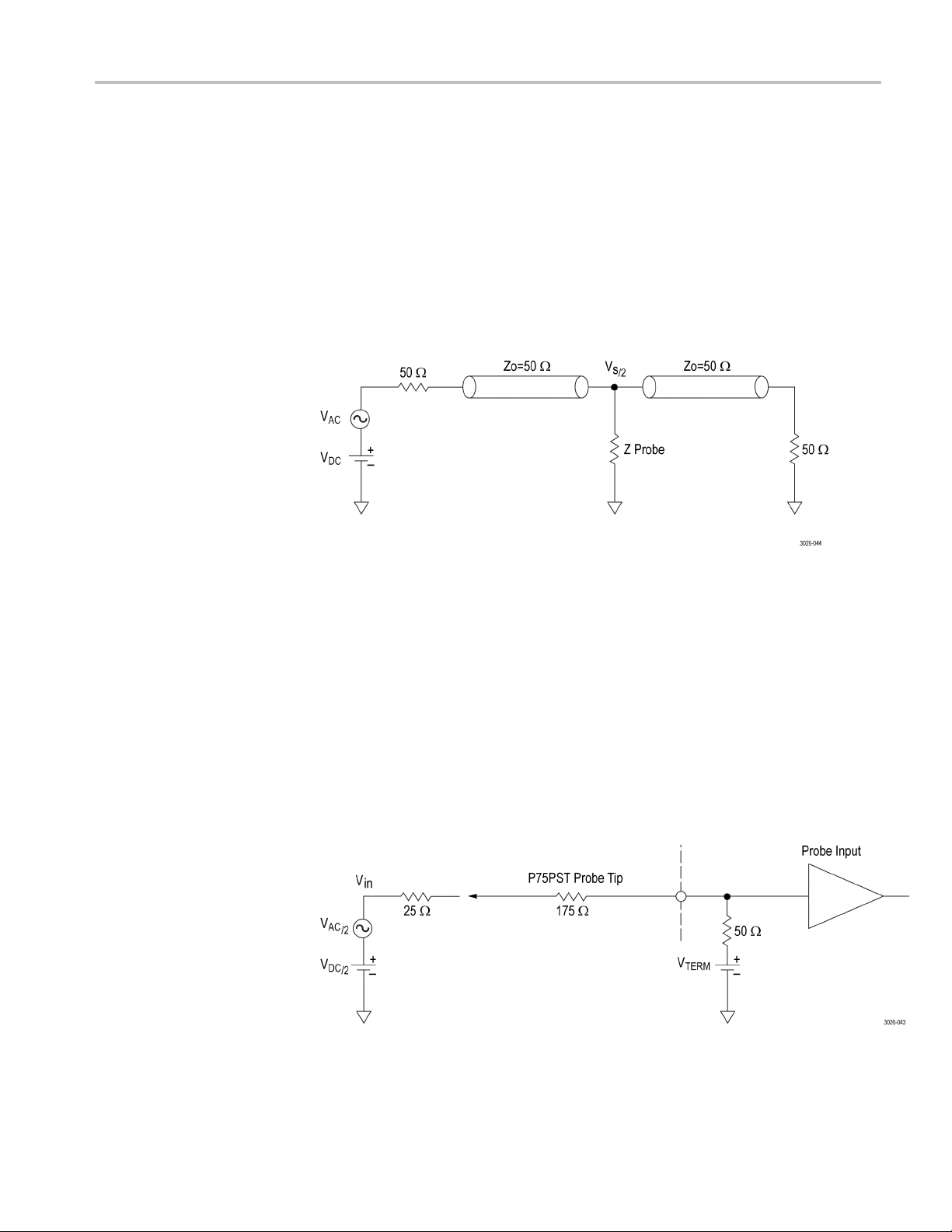
Coaxial Adapters
Each input of the P76CA–xxx adapters provides a 50 Ω transmission line signal
path from its input connector to the termination resistor at the probe amplifier
input. (See Figure 10.) A P7630 probe coaxial tip simplified input schematic
is shown in the figure below.
Figure 10: TriMode probe coaxial input model
The high frequency signals that the P7630 probe is designed to measure typically
have a 50 ohm source impedance, as shown in the above schematic. The DUT
l, V
signa
, is transmitted to the P7630 probe coaxial tip through a 50 ohm
S
transmission line. The P7630 probe input termination resistor is intended to
provide a low discontinuity termination for the DUT signal.
The DUT signal source, V
, is represented in the above schematic as appearing at
S
the input to the P7630 probe coaxial adapter. The P7630 probe coaxial adapters
are calibrated to the adapter connectors for either AC or DC signals and are
compensated for the small DC signal loss in the coaxial adapter signal path.
The signal g ain through the P7630 probe amplifier, when used with a coaxial
adapter, is represented as a unity gain factor multiplied times the selected step
gain. The probe amplifier step gain is selected by the host oscilloscope control
nterface, based on the user-selected vertical scale factor for the vertical channel
i
to which the probe is attached.
14 P7630 TriMode Probe Technical Reference
Page 29
Theory of Operation
Solder Tip Adapter
The P76TA adapt
Series TriMode probe tips to be attached to a P7630 probe. P7500 Series probe
tips have a nominal 5X attenuation structure when used with a 50 Ω input
termination device like the P7630 p robe.
The use of a passive attenuation input pick-off resistor at the P7500 Series probe
tip means that the P7630 probe acts like a Z0 probe when used with a P76TA
adapter and P7500 Series probe tip. This 5X Z0 probe structure reduces probe
loading enough that it is possible to use the P7630 probe and P76TA adapter for
making pro
as shown in the simplified schematic below. (See Figure 11.)
Figure 11: P76TA adapter simplified schematic
er provides a probe tip connection interface that enables P7500
bing measurements anywhere along the signal transmission line path,
The probe diagram above shows a probe measurement being made on a
doubly-terminated signal path. This doubly-terminated signal path is a common
structure for many high frequency signaling standards, since, if implemented
correctly, it p rovides a very low-discontinuity signal path.
The 50 Ω back termination at the signal transmitter absorbs reflected signals
from reverse-path discontinuities on the signal transmission line, including those
due to probe loading. The additional 50 Ω termination resistor at the end of the
ansmission line path also serves to absorb the transmitted signal power and any
tr
forward-path signal reflections from discontinuities on the signal transmission
line. This doubly-terminated signal structure results in an effective 2 5 ohm signal
source impedance. (See Figure 12.)
Figure 12: P76TA adapter and P75PST tip equivalent schematic
P7630 TriMode Probe Technical Reference 15
Page 30

Theory of Operation
Scale Factor
In many of the high-frequency signaling standards that the P7630 probe is
designed for, a 50 Ω termination at the transmitter is in parallel with another 50 Ω
termination
signal source impedance. (See Figure 12.)
at the end of the transmission line path, effectively making a 25 Ω
When the P76
DUT within the transmission line path, this 25 Ω source impedance must be
considered a part of the probe input attenuator structure, and therefore be included
when calculating the probe gain.
Using the formula:
Ext Atten = (Rsource + 225 Ω)/225Ω
where th
differential input, substituting 25 Ω for the Rsource impedance yields an external
attenuation factor of 1.1116.
The probe/oscilloscope signal gain is factory-calibrated at the P76TA probe tips
using this external attenuation factor of 1.1116, and is accurately scaled by the
vertical volts/div control on the host oscilloscope.
For systems with source impedances not equal to 25 Ω, it may be necessary to
adjust the oscilloscope EXT ATTEN scale factor and the offset voltage to optimize
the measurement accuracy. You may also need to adjust the probe termination
voltage control to null out the DC loading effect of the probe.
TA adapter and P75PST or P75TLRST tips are used to probe the
e225Ω represents the input resistance of one half of the solder tip
16 P7630 TriMode Probe Technical Reference
Page 31
Probing Techniques to Maximize Measurement Fidelity
Measurement fidelity is an indication of how accurately a probe represents the
signal being measured. The measurement fidelity of the probe is best when
the probe is connected to the circuit with the P76CA-xxx probe adapters. The
P76CA-292C and P76CA-SMP adapters both include a pair of 6 inch, low-loss,
skew-match
ideally matched high-quality cables to complete the connection to your circuit.
When you use the P76TA adapter with P7500 series probe tips, proper wire lead
length is critical for achieving good measurement results. Recommendations for
connecting the P7500 probe tips a re given in the following section.
The P7630 probe contains S-parameter characterization data for the probe, which
is downloaded to the attached oscilloscope when the probe is first connected. This
probe-specific data is used along with nominal probe adapter data to generate
DSP correction filters that are used for improved high f requency measurement
accuracy. After the probe adapter is attached to the probe, the adapter transfers
identification data which is used as part of the generated filter process.
ed cables. When using the P76CA-292 adapter, only use matched,
Theory of Operation
P76CA-xxx Adapters
P76TA Adapter with P7500
TriMode Solder Tips
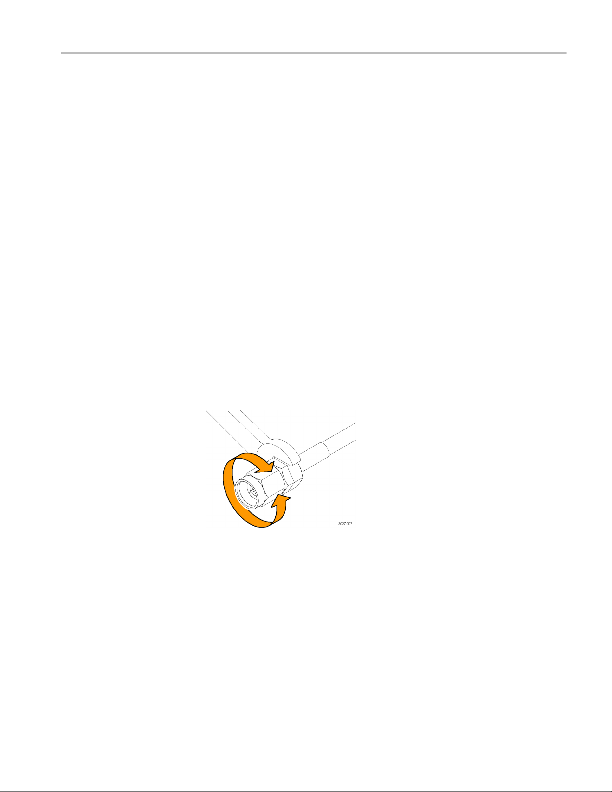
To prevent damage and prolong connector and cable life, the cable and center
conductors must not twist when making connections. Always use a wrench to
minimize the cable twist when you connect and disconnect the 2.92 adapters and
cables. Use a torque wrench to tighten the connectors to 8 in-lbs. Failure to do so
will shorten the service life of the adapters.
Figure 13: Preventing twist to the coaxial input cables
There are several solder tips available for connecting the P7500 Series probes
to your circuit. The P75PST and P75TLRST probe tips solder directly to your
circuit through small wires. (See Figure 14 on page 18.) Two resistor solder tips
are also available; these tips include input resistors that solder to your circuit and
can be replaced if damaged.
P75PST and P75TLRST TriMode Solder Tips. The P75PST and P75TLRST probe
tips are each composed of a small form factor interconnect circuit board with
SMD0402 damping resistors and a set of vias for wire attachment to the DUT
P7630 TriMode Probe Technical Reference 17
Page 32

Theory of Operation
(Device Under T
8 mil wire, and a special high tensile strength wire is supplied as part of the wire
accessory kit. The expanded view of the probe tips shows the location of the A
and B signal inputs as well as the two ground reference connections.
Figure 14: P75PST and P75TLRST TriMode Solder Tips
The recommended wire attachment method is to first solder the wires to the DUT,
being careful to minimize the wire length of the signal and ground connections.
Next, attach a solder ramp to the bottom of the solder tip with hot g lue. A kit of
r ramps are included with the P76TA adapter. A notch on the ramp aligns
solde
with the bottom of the tip.
est). The circuit board vias are designed for both 4 mil and
Figure 15: Solder ramp installed
The solder ramps are designed to point the front of the solder tip downward to
minimize the distance between the solder points on the solder tip and the circuit
st points. For signal frequencies that exceed 25 MHz, this distance must be less
te
than 0.032 in. (0.8 mm) to achieve good results.
nce the solder ramp is secured to the tip, thread the wires through the probe tip
O
board vias, being careful to achieve as symmetrical a wire pattern as possible
between the two signal inputs and a very short ground connection. Secure the
tip/ramp assembly to the DUT with tape or hot glue, and finally, solder the wires
on top of the probe tip circuit board. Any excess wire lead length extending
through the probe tip board should be removed to minimize possible signal
reflection problems.
18 P7630 TriMode Probe Technical Reference
Page 33

Theory of Operation
Because of the l
tip circuit board, the solder-down probe tip should be taped down at the DUT for
strain relief. Although the accessory kit includes adhesive strips that can be used
for the strain relief of the probe tip, the use of mylar tape will generally provide
stronger attachment if room is available at the DUT.
Probe Tip Ca
of very low skew (<1ps) coaxial cables and a polarized G3PO dual connector
block. The 3GPO connectors use a miniature, high frequency design that enables
quick and easy installation of the P7500 Series solder tips. The G3PO connector
block of the probe tip is inserted into the input of the P76TA adapter. The
adapter contains a mating, polarized G3PO connector block with attached G3PO
connecto
The connector bullets are a part of the G3PO connector design, providing a
self-al
connector in the adapter is designed to have higher detent force than the probe
tip connectors, which is intended to ensure that the G3PO bullets remain in the
P76TA adapter connector when disconnected. The adapter, with its integral
spring mechanism, helps to provide a self-aligning mechanism for hand insertion
of the probe tip. The adapter springs also give a secure capture of the probe
tip c
wire-connected cable release holder on the probe tip connec tor. This probe tip
release holder should always be used rather than pulling on the probe tip cables,
which may cause tip cable damage.
r bullets.
igning interconnect mechanism between G3PO connectors. The G3PO
onnector after insertion. Release of the probe tip is assisted by using the
imited mechanical strength of the wire interconnect and probe
bles and Connectors. Attached to the probe tip circuit board is a pair
P7630 TriMode Probe Technical Reference 19
Page 34

Theory of Operation
DUT Connection
between the probe tip board and the DUT must be kept as short as possible to
preserve the integrity of the measured signal. Typical wire lengths range from
0.010 in. to 0.100 in. (See Figure 16.)
s. The lead length of the resistor leads and connection wires
Figure 16: Typical wire length from probe tip to circuit
The following four figures illustrate the signal integrity effect on the P75TLRST
solder tip when used with different lengths of tip wire. Signal fidelity is best when
the wire length is kept as short as possible. The step generator that was used as
a signal source for these screenshots has a 30 ps 10-90% rise time. The table in
each figure contains data for two rise time measurements (10-90% and 20-80%).
These screenshots can be used as a rough guide to gauge the effects of wire length,
but actual results may vary depending on the other factors like characteristics of
e device under test (for example, rise time and impedance), precision of the
th
solder connection, and the model of oscilloscope.
20 P7630 TriMode Probe Technical Reference
Page 35

Figure 17: P75TLRST solder tip with 0.010 in. of tip wire
Theory of Operation
Figure 18: P75TLRST solder tip with 0.050 in. of tip wire
P7630 TriMode Probe Technical Reference 21
Page 36

Theory of Operation
Figure 19: P75TLRST solder tip with 0.100 in. of tip wire
Figure 20: P75TLRST solder tip with 0.200 in. of tip wire
22 P7630 TriMode Probe Technical Reference
Page 37

Reference
This section contains information about taking measurements with the probe
and increasing measurement accuracy.
Single-Ended Measurements Using A and B Modes
A differential probe such as the P7630 TriMode Probe can be used for single-ended
measurements within the limits of its dynamic and offset voltage ranges.
Single-ended probes such as the P7240 typically have a wider offset range than
differential probes, but with much lower bandwidth performance. (See Table 1.)
Table 1: Offset ranges
Probe Attenuation DC offset Dynamic range
P7240 5X
P7513 & P7516 (differential mode)
P7513 & P7516 (single-ended and common-mode)
P7520 (differential mode)
P7520 (single-ended and common-mode)
1
P7630
Coaxial adapters
5X +2.5 V, -1.5 V 1.5 V
5X +3.4 V, -1.8 V 1.5 V
5X +2.5 V, -1.5 V 1.25 V
5X +3.4 V, -1.8 V 1.25 V
1X
1X
Solder tip adapter
5X
5X
1
The P7630 probe has independent A and B input offset controls
ground or the reference level of the measured signal. S et the A signal offset to the DC common-mode voltage of the measured signal.
. To take a single-ended m easurement, use the B input for reference and set the B offset to
+/- 5 V
+/- 4 V 1.2 VPP(single-ended)
+/- 4 V 2.0 V
+/- 4 V 6.0 V
+/- 4 V 10.0 V
4V
PP
PP
PP
PP
PP
(differential)
PP
(single-ended)
PP
(differential)
PP
Differential probes are ideal for a class of single-ended measurements where the
reference voltage is not ground:
SSTL_1,2: VTT,V
PECL: V
=VCC-1.3
REF
REF
=VDD/2
To measure single-ended s ignals in this class, connect the B input of the P7630
Probe to V
REF
.
A differential probe in these applications displays the true signal despite any AC
or DC variation in V
the signal plus the variation in V
from its nominal value. A single-ended probe displays
REF
. Differential probes can also be used to make
REF
ground referenced single-ended measurements o n either single-ended signals or
differential signals like PCI Express or Serial ATA.
Single-ended measurements on differential signals are used to measure common
mode voltage and check for differential signal symmetry. By using a TriMode
probe, you can easily take these measurements with one adapter connection (two
coax cables or a grounded solder tip). Cycle the Input Mode switch to display the
signal that you want to view.
P7630 TriMode Probe Technical Reference 23
Page 38

Reference
Differential
Measurements
A differential probe is optimized to measure high speed differential signals.
Differential signals are formed from two complementary signals with a common
reference vo
Devices designed for differential measurements avoid problems presente d by
single-ended systems. These devices include a variety of differential probes,
differential amplifiers, and isolators.
A differential probe is basically a differential amplifier, which is used to make
differential measurements that reject any voltage that is common to the inputs and
amplifies any difference between the inputs. Voltage that is common to both
inputs is often referred to as the Common-Mode Voltage (V
is different as the Differential-Mode Voltage (V
ltage. (See Figure 21.)
DM
) and voltage that
CM
).
Common-Mode Rejection
Ratio
Figure 21: Simplified model of a differential amplifier
Differential amplifiers cannot reject all of the common-mode signal. The ability
of a differential amplifier to reject the common-mode signal is expressed as the
Common-Mode Rejection Ratio (CMRR).
The DC CMRR is the differential-mode gain (A
gain (A
). It is expressed either as a ratio or in dB:
CM
) divided by the common-mode
DM
AC CMRR for the P7630 probe is defined using 3-port, mixed-mode S-parameters
as:
for the measured differential mode response, where A input = S1, B input
= S2 and Output = S3. The 6 dB term in the AC CMRR equation gives the
voltage-referenced response. CMRR generally is highest (best) at DC and
degrades with increasing frequency. A typical CMRR plot for the P7630 probe is
shown. (See Figure 22 on page 25.)
24 P7630 TriMode Probe Technical Reference
Page 39
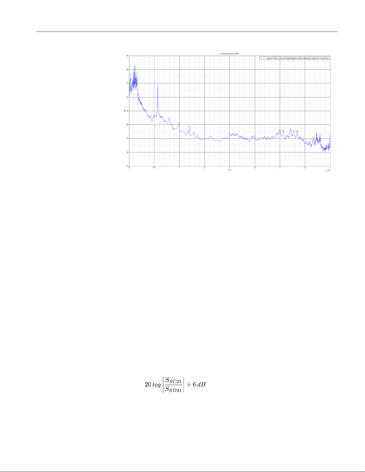
Figure 22: Typical CMRR
Reference
Assessing CMRR Error
Input Imped ance Effects
on CMRR
Differential-Mode
Rejection
The CMRR of the P7630 TriMode Probe is shown in graphs assuming a sinusoidal
common-mode signal. A quick way to assess the magnitude of CMRR error
when the common-mode signal is not sinusoidal is to connect both leads to the
same point in the circuit. The oscilloscope displays only the common-mode
component that is not fully rejected by the probe. While this technique may n ot
yield accurate measurements, it does allow you to determine if the magnitude of
the common-mode error signal is significant. When using the solder-down tips,
keep the tip leads the same length to maximize the probe CMRR.
The lower the input impedance of the probe relative to the source impedance,
thelowertheCMRRforagivensourceimpedance imbalance. Differences
in the source impedance driving the two inputs lowers the CMRR. Note that
single-ended measurements generally result in asymmetric source impedances
which tend to reduce the differential mode CMRR.
When making common-mode signal measurements (A+B/2 – GND) with the
TriMode probe, it is desirable to reject the differential-mode signal present
between the two inputs. This rejection is expressed as the Differential-Mode
Rejection Ratio (DMRR).
AC DMRR for the P7630 probe is defined using 3-port, mixed-mode S-parameters
as:
for the measured common mode response. The 6 dB term in the AC DMRR
equation gives the voltage-referenced response.
P7630 TriMode Probe Technical Reference 25
Page 40

Reference
Channel Isolation
Under ideal con
ditions when taking single-ended measurements with a differential
probe, no part of a signal applied to one input of the probe would appear on the
other input. In reality some portion of the signal on one input does “bleed” over to
the other input, and this effect increases with frequency. Channel isolation is a
measure of how much crosstalk occurs between the two probe inputs. The channel
isolation is defined with S-parameter measurements below, where:
A input = S1, B input = S2, Output = S3
A ISOLATION = 20 log (S
B ISOLATION = 20 log (S
31/S32
32/S31
) | A Mode
)|BMode
A typical isolation plot for the P7630 TriMode probe using a coaxial adapter
is shown below. When the probe is used with the P76TA adapter and solder
tips, note that channel isolation performance is highly dependent on probe tip
attachment lead length. Good channel isolation requires keeping the interconnect
lead length for both signal and ground connections very short. (See Figure 23.)
Figure 23: Typical channel isolation
26 P7630 TriMode Probe Technical Reference
Page 41

Specifications
Specification
s
These specifi
cations apply to the P7630 TriMode Probe when installed on
a DPO/DSA73304D oscilloscope. The probe and oscilloscope must have a
warm-up period of at least 20 minutes and be in an environment that does not
exceed the allowed limits. (See Table 3.)
Specifications for the P7630 TriMode Probe fall into three categories: warranted,
typical, and nominal characteristics.
Warranted Characteristics
Warranted characteristics describe guaranteed performance within tolerance limits
or certain type-tested requirements.
Table 2: Warranted electrical characteristics
Coaxial adapters Solder tip adapter
Characteristic P76CA-292 P76CA-292C P76CA-SMP P76TA
Rise time, system,
DSP corrected
10% – 90%
20% – 80%
DC gain accuracy ±2% ±2% ±2% ±2%
DC output zero
common mode
imbalance
Operating voltage
window
Input signal range
Linearity
Offset voltage range
Offset voltage accuracy
(referred to input)
DC offset drift
(referred to input)
Termination voltage
range
Termination voltage
accuracy
1
Single-ended
Differential
<16 ps <16 ps <16 ps <16 ps
<12 ps <12 ps <12 ps <12 ps
±4 mV ±4 mV ±4 mV ±4 mV
-4.0Vto+4.0V -4.0Vto+4.0V -4.0Vto+4.0V -5.0Vto+5.0V
1.2 Vp-p 1.2 Vp-p 1.2 Vp-p 6.0 Vp-p
2.0 Vp-p 2.0 Vp-p 2.0 Vp-p 10.0 Vp-p
±1% ±1% ±1% ±1%
–4.0 V to +4.0 V –4.0 V to +4.0 V –4.0 V to +4.0 V –4.0 V to +4.0 V
±(2% of FS range +
6mV)
<±0.2 mV/ °C <±0.2 mV/ °C <±0.2 mV/ °C <±0.2 mV/ °C
-4.0Vto+4.0V -4.0Vto+4.0V -4.0Vto+4.0V -4.0Vto+4.0V
<±10 mV <±10 mV <±10 mV <±10 mV
±(2% of FS range +
6mV)
±(2% of FS range +
6mV)
±(2% of FS range +
30 mV) (25 Ω source Z)
P7630 TriMode Probe Technical Reference 27
Page 42

Specifications
Table 2: Warranted electrical characteristics (cont.)
Coaxial adapters Solder tip adapter
Characteristic P76CA-292 P76CA-292C P76CA-SMP P76TA
Maximum
nondestructive input
2
voltage
Input impedance
Differential 450 Ω @1 GHz
Single-ended 225 Ω @1 GHz
Input return loss
Freqto5GHz
Freq to 20 GHz
Freq to 30 GHz
Noise
Probe only (most
sensitive range)
System, DSP
corrected (most
sensitive range)
Overload indicator
range (P76CA-xxx
adapters only)
1
Measured at the output of the probe, relative to the DC output zero common mode voltage reported as the calibrated value in the TekConnect message for
each step gain and input mode combination.
2
Measured between each input or between either probe input and ground.
±5 V
(DC + peak AC)
±5 V
(DC + peak AC)
±5 V
(DC + peak AC)
±8 V
(DC + peak AC)
200 Ω @10 GHz
150 Ω @25 GHz
150 Ω @10 GHz
100 Ω @25 GHz
>20 dB >20 dB >20 dB
>12 dB >12 dB >12 dB
>10 dB >10 dB >10 dB
<0.9 mVrms <0.9 mVrms <0.9 mVrms
<1.0 mVrms <1.0 mVrms <1.0 mVrms <5.0 mVrms
Vterm
Overload off Overload on
–4 V –4.25 <Vin< –1.75 Vin< –4.75 or Vin> –1.00
–3 V –4.25 <Vin< –0.75 Vin< –4.75 or Vin> –0.15
–2 V –4.25 <Vin< +0.25 Vin< –4.75 or Vin> +0.75
–1 V –3.25 <Vin< +1.25 Vin< –3.75 or Vin> +1.75
0 V –2.25 <Vin< +2.25 Vin< –2.75 or Vin> +2.75
+1 V –1.25 <Vin< +3.25 Vin< –1.75 or Vin> +3.75
+2 V +0.25 <Vin< +4.25 Vin< –0.75 or Vin> +4.75
+3 V +0.75 <Vin< +4.25 Vin< +0.25 or Vin> +4.75
+4 V +1.75 <Vin< +4.25 Vin< +1.25 or Vin> +4.75
28 P7630 TriMode Probe Technical Reference
Page 43

Specifications
Table 3: Warran
Characteristic Specification
Temperature
Operating 0 to 40 °C (+32
Nonoperating
Humidity
Operating 20–80% RH, at up to +40 °C (+104 °F)
Nonoperating
Altitude
Operating 3000 meters (10,000 feet)
Nonoper
ted environmental characteristics
ating
to +104 °F)
–20 to +60 °C
12,000 meters (40,000 feet)
(–4 to +140 °F)
5–90% RH
P7630 TriMode Probe Technical Reference 29
Page 44

Specifications
Typical Chara
cteristics
Typical characteristics describe typical but not guaranteed performance.
Table 4: Typical electrical characteristics
Coaxial adapters Solder tip adapter
Characteristic P76CA-292 P76CA-292C P76CA-SMP P76TA
Bandwidth
Rise time, probe only
Input sense voltage
accuracy
Common-mode
rejection ratio,
differential-mode
Differential-mode
rejection ratio,
common-mode
Channel isolation,
single-ended mode
1
2
1
Probe only
System, DSP
corrected
10% –90%
20% –80%
2
Measurements taken @18 to 28 ºC (+64 to +82 °F)
The voltages on the probe inputs are sensed by the probe circuitry, and are used to generate voltages associated with the Set buttons on the oscilloscope
GUI. The Set buttons are used to automatically enter these generated Offset and Termination voltages in the on-screen fields; either Individually or Mean
values can be selected.
>30 GHz
(all input modes)
>30 GHz
(all input modes)
Input sense voltage =
Vin ±24 mV
>40dB@DC >40dB@DC >40dB@DC
>14dBto15GHz >14dBto15GHz >14dBto15GHz
>6 dB to 30 GHz >6 dB to 30 GHz >6 dB to 30 GHz
>26dBto20GHz >26dBto20GHz >26dBto20GHz
>18dBto30GHz >18dBto30GHz >18dBto30GHz
>20dBto20GHz >20dBto20GHz >20dBto20GHz
>12dBto30GHz >12dBto30GHz >12dBto30GHz
>30 GHz
(all input modes)
<16 ps
<12 ps
Input sense voltage
=Vin±24mV
>30 GHz
(all input modes)
Input sense voltage
=Vin±24mV
>30 GHz (A, B, D modes)
>25 GHz (common mode)
Input sense voltage
= Vin ±100 mV
able 5: Typical mechanical characteristics
T
Characteristic Description
imensions, control box
D
Dimensions, probe body
Dimensions, probe main cable length
Unit weight
125.4 mm × 41 mm × 35 mm (4.9 in × 1.6 in × 1.4 in)
101.6 mm × 8.89 mm × 19 mm (4.0 in × 0.350 in × 0.750 in)
1.2 m (47.2 in) (from the front of the probe body to the rear of the
control box; does not include adapter)
1.860 kg (4.1 lbs) (probe, accessories and packaging)
30 P7630 TriMode Probe Technical Reference
Page 45

Specifications
The following fi
probe.
gures show the typical rise time and frequency response of the
Figure 24: Typical rise time
ure 25: Typical frequency response
Fig
P7630 TriMode Probe Technical Reference 31
Page 46

Specifications
igure 26: Probe body and control box dimensions
F
32 P7630 TriMode Probe Technical Reference
Page 47

Specifications
Figure 27: P7630 Probe adapter dimensions
Figure 28: P75PST and P75TLRST solder tip dimensions
P7630 TriMode Probe Technical Reference 33
Page 48

Specifications
Nominal Chara
cteristics
Nominal characteristics describe guaranteed traits, but the traits do not have
tolerance limits.
Table 6: Nom
Characteristic P76CA-292 P76CA-292C P76CA-SMP P76TA
Maximum po
dissipation
Terminat
Probe tip N.A. N.A. N.A. 62.5 mW
Input resistance
Input capacitance N.A. N.A. N.A. 0.1 pF
1
P75PST and P75TLRST solder tips
Table 7
Characteristic Connector type Description
Input configuration
1
User-supplied cables
inal electrical characteristics
Coaxial adapters Solder tip adapter
wer
ion resistor
125 mW 125 mW 125 mW N.A.
50 Ω ±2 Ω 50 Ω ±2 Ω 50 Ω ±2 Ω 225 Ω
: Nominal adapter electrical characteristics
P76CA–292 Adapter 2.92 mm coaxial female
P76CA–292C Adapter 2.92 mm coaxial male (cables)
P76CA–SMP Adapter SMP coaxial female (cables)
TA Adapter with:
P76
PST solder tip
P75
5TLRST solder tip
P7
0.012 in-diameter solder vias
0.012 in-diameter solder vias
1
Differential (two coaxial signal inputs, A and B; outer
cable shields are grounds)
ferential (two signal inputs, A and B; shared with
Dif
single-ended)
Single-ended (one each A and B signal input and
o ground inputs)
tw
1
34 P7630 TriMode Probe Technical Reference
Page 49

User Service
Error Condition
This section covers troubleshooting and probe maintenance. If your probe does
not meet the specifications listed in the Specifications, you can send the probe to
Tektronix fo
r calibration and repair. (See page 40, Preparation for Shipment.)
The LEDs on
the probe alert you to error or status conditions affecting the probe.
When the probe is functioning correctly, there is a quick flash of the LEDs on
the probe just after connecting to the oscilloscope. If the probe LEDs flash or
otherwise appear to be malfunctioning, an error condition may exist. Disconnect
the probe and reconnect it to another channel to isolate the problem. If the
symptoms persist with the probe, call your Tektronix representative for service.
Replaceable Parts
The following parts may need to be replaced due to normal wear and damage.
When yo
to simplify the procedure.
Table 8: TriMode probes replaceable parts
Description Replacement part number
0 probe body bullet contacts
P763
A adapter bullet contacts
P76T
P75PST & P75TLRST solder tip wires
See the user manual for a list of the accessories that are available for your probe.
u replace these components, secure the probe in a small vise or positioner
020-3105-xx, kit of 4
013-0359-xx, kit of 4
-2754-xx, Wire Replacement Kit, includes one bobbin each:
020
4 mil wire, 8 mil wire, and SAC305 solder
Table 9: Required equipment
Description Minimum requirement Recommended example
P7630 probe body bullet removal tool 003-1934-xx
76TA adapter bullet removal tool
P
Probe positioner or bench vise Able to hold probe PPM203B or PPM100
Magnifying glass or microscope Free standing to allow hands-free use
Tweezers
1
Nine-digit part numbers (xxx-xxxx-xx) are Tektronix part numbers.
General purpose
03-1896-xx
0
1
P7630 TriMode Probe Technical Reference 35
Page 50

User Service
Replacing the Bullet
Contacts
The bullet cont
replaced every 200 insertion cycles. The bullet contacts and removal tool differ in
size between the two and cannot be interchanged. The P76TA components are
larger, but the procedures are similar for both the probe and adapter.
To replace the bullets, use the bullets and bullet removal tool listed in the tables
above, and follow the steps below.
Remove.
1. Squeeze the tool plunger to extend the holder tangs.
2. Insert the tool into the probe body or adapter so that the holder tangs surround
one of the bullets.
3. Release the plunger to secure the holder tangs on the bullet.
4. Gently pull the tool outward to remove the bullet.
5. Repeat for the other bullet.
CAUTION. If you cannot extract the bullets with the bullet removal tool, use fine
needle-nosed pliers and a m agnifying glass or microscope. Be careful not to
damage the probe adapter with the pliers.
acts in the P7630 probe head and P76TA adapter should be
Figure 29: Removing the bullets
36 P7630 TriMode Probe Technical Reference
Page 51

User Service
Install. When b
following:
1. Squeeze the to
2. Insert a new bullet into the tool so that the holder tangs surround the bullet.
3. Release the plunger to secure the holder tangs on the bullet.
4. Insert the tool into the probe body or adapter and seat the bullet in the recess.
5. Squeeze the tool plunger to release the bullet.
6. Gently pull the tool out of the probe or adapter.
7. Repeat fo
8. Test that the bullets are installed correctly by connecting and then removing
the P76T
probe adapter. Inspect the probe or adapter and verify that the bullets remain
seated in the probe or adapter (where you installed them).
oth bullets have been removed, install new bullets by doing the
ol plunger to extend the holder tangs.
r the other bullet.
A adapter from the probe, or an accessory solder tip to and from the
Figure 30: Installing the bullets
P7630 TriMode Probe Technical Reference 37
Page 52

User Service
P75PST & P75TLRST
Solder Tip Wires
The solder vias
solder tips are small (0.012 in.), and require small wires to attach to your circuit.
(Use the 4-mil and 8-mil wires included with the Wire Replacement kit to make
the connections.) Because of the small dimensions, the solder tips have a limited
number of solder cycles that the vias can withstand before the Solder Tips become
unusable. If you expect to make frequent soldering changes, consider using the
optional Tr
can accept a higher number of solder cycles and can be replaced when necessary.
NOTE. Axial-leaded tip resistors (included in the TriMode resistor replacement
kit, Tektronix part number 020-2937-xx), should not be used in place of wires
with the P75PST and P75TLRST probe tips unless the surface-mount, SMD0402
resistors are also changed. The total probe tip resistance for the P7500 Series
solder t
CAUTION. To prevent damage to the circuit board or circuit board connections
due to a
you secure the tip to the circuit board using the adhesive tip tape provided in your
accessory kit. You can also use other materials such as Kapton tape or hot glue.
To avoid damage to the tip or the circuit under test, avoid applying excessive heat
from the soldering iron. Use a low wattage, temperature-controlled soldering iron
and appropriately sized soldering iron tip.
ipsisdesignedtobe175Ω.
ccidental movement of the probe and soldered leads, we recommend that
on the circuit board at the end of the P75PST and P75TLRST
iMode Resistor solder tips. The resistors that extend off of these tips
To prolong the life of your solder tips, consider the following points before you
use the solder tips.
Consider the types of measurements that you plan to take. If you are going to take
a few measurements at one location and then move to another, you may be able to
use longer wires. Longer wires may degrade your measurement slightly (which
may not matter), but the wires can then be cut or de-soldered at your circuit and
eused, rather than subjecting the solder tip to a de solde r/solder cycle.
r
At critical test points such as circuit outputs, you might need to keep the wires
as short as possible. If possible, use the solder tip dimensions shown in the
Specifications section to lay out a matching footprint on your circuit board.
38 P7630 TriMode Probe Technical Reference
Page 53

User Service
Use the followi
For best soldering results, use a microscope to examine the quality of the
solder joints
Use a low-wattage, temperature-controlled soldering iron and a small mass
soldering i
possible, while still providing a reliable solder joint.
Use SAC305 s
wires to the circuit under test.
When repla
remove the excess solder from the probe tip circuit board via holes. Be careful
not to overheat the via and damage the board.
The attachment wires should be bent symmetrically to vary the interconnect
spacing. Use care when you solder a tip to a circuit under test to avoid
inadvertently de-soldering either the attachment wires or the damping resistor.
For optimum performance and signal integrity, keep the lead length between
the DUT (Device Under Test) and the tip as short as possible, and the lead
lengths the same length.
ng precautions when you solder the tips:
.
ron tip. The soldering iron temperature should be set as low as
older (included with the wire replacement kit) to attach the tip
cing tip wires or axial-lead resistors, solder wick can be used to
P7630 TriMode Probe Technical Reference 39
Page 54

User Service
Preparation f
or Shipment
If the original packaging is unfit for use or not available, use the following
packaging guidelines:
1. Use a corrugated cardboard shipping carton having inside dimensions at least
2. Put the probe into an antistatic bag or wrap to protect it from dampness.
3. Place the probe into the box and stabilize it with lightweight packing material.
4. Seal the carton with shipping tape.
5. Refer to Contacting Tektronix on the copyright page of this manual for the
one inch greater than the probe dimensions. The box should have a carton
test streng
shipping address.
th of at least 200 pounds.
40 P7630 TriMode Probe Technical Reference
Page 55

Index
A
Autoset, 12
C
Channel iso
Characteristics
Mechanical, 31
nominal, 34
CMRR, 24
assessing CMRR error, 25
Coaxial a
lation, 26
dapters, 14
D
Differential measurements, 24
Differential-Mode Rejection
Ratio, 25
DUT connections, 20
E
Error condition, 35
I
Input impedance, 14
Input signal
Input voltage, 8
dynamic range, 9
O
Offset voltage, 10, 12
Operating voltage window, 9
P
P75PST & P75TLRST
solder tip wires, 38
P75PST a
P76TA, 15
Preparation for Shipment, 40
Probe
Probe input architecture, 5
Probing techniques, 17
nd P75TLRST
TriMode solder tips, 17
replacing the bullet
contacts, 36
components, 1
R
Replaceable parts, 35
Rise time, 31
S
Safety Summary, iv
Scale factor, 16
Single-ended measurements, 23
Specifications
typical, 30
warrante
d, 27
T
Termination voltage, 11, 13
TriMode operation, 6
U
User service, 35
F
quency response, 31
Fre
P7630 TriMode Probe Technical Reference 41
 Loading...