

Page 1

x
P7520A
TriMode™ Probe
ZZZ
Instruction Manual
*P071304800*
071-3048-00
Page 2

Page 3

xx
P7520A
TriMode™ Probe
ZZZ
Instruction Manual
www.tektronix.com
071-3048-00
Page 4

Copyright © Tektronix. All rights reserved. Licensed software products are owned by Tektronix or its subsidiaries or suppliers, and are
protected by na
tional copyright laws and international treaty provisions.
Tektronix pro
previously published material. Specifications and price change privileges reserved.
TEKTRONIX and TEK are registered trademarks of Tektronix, Inc.
EZ-Probe is a registered trademark of Cascade Microtech, Inc.
TriMode is a trademark of Tektronix, Inc.
ducts are covered by U.S. and foreign patents, issued and pending. Information in this publication supersedes that in all
Contacting Tektronix
Tektronix, Inc.
14150 SW Karl Braun Drive
P.O. Box 500
Beaverton, OR 97077
USA
For product information, sales, service, and technical support:
In North America, call 1-800-833-9200.
Worldwide, visit www.tektronix.com to find contacts in your area.
Page 5

Warranty
Tektronix warrants that this product will be free from defects in materials and workmanship for a period of one (1) year from the date of
shipment. If any such product proves defective during this warranty period, Tektronix, at its option, either will repair the defective
product without charge for parts and labor, or will provide a replacement in exchange for the defective product. Parts, modules and
replacement products used by Tektronix for warranty work may be new or reconditioned to like new performance. All replaced
parts, modules and products become the property of Tektronix.
In order to obtain service under this warranty, Customer must notify Tektronix of the defect before the expiration of the warranty period
and make suitable arrangements for the performance of service. Customer shall be responsible for packaging and shipping the
defective product to the service center designated by Tektronix, with shipping charges prepaid. Tektronix shall pay for the return of the
product to Customer if the shipment is to a location within the country in which the Tektronix service center is located. Customer shall
be responsible for paying all shipping charges, duties, taxes, and any other charges for products returned to any other locations.
This warranty shall not apply to any defect, failure or damage caused by improper use or improper or inadequate maintenance and
care. Tektronix shall not be obligated to furnish service under this warranty a) to repair damage resulting from a ttempts by personnel
other than Tektronix representatives to install, repair or service the product; b) to repair damage resulting from improper use or
connection to incompatible equipment; c) to repair any damage or malfunction caused by the use of non-Tektronix supplies; or
d) to service a product that has been modified or integrated with other products when the effect of such modification or integration
increases the time or difficulty of servicing the product.
THIS WARRANTY IS GIVEN BY TEKTRONIX WITH RESPECT TO THE PRODUCT IN LIEU OF ANY OTHER WARRANTIES,
EXPRESS OR IMPLIED. TEKTRONIX AND ITS VENDORS DISCLAIM ANY IMPLIED WARRANTIES OF MERCHANTABILITY OR
FITNESS FOR A PARTICULAR PURPOSE. TEKTRONIX' RESPONSIBILITY TO REPAIR OR REPLACE DEFECTIVE PRODUCTS
IS THE SOLE AND E XCLU S IVE REMEDY PROVIDED TO THE CUSTOMER FOR BREACH OF THIS WARRANTY. TEKTRONIX
AND ITS VENDORS WILL NOT BE LIABLE FOR ANY INDIRECT, SPECIAL, INCIDENTAL, OR CONSEQUENTIAL DAMAGES
IRRESPECTIVE OF WHETHER TEKTRONIX OR THE VENDOR HAS ADVANCE NOTICE OF THE POSSIBILITY OF SUCH
DAMAGES.
[W2 – 15AUG04]
Page 6

Page 7

Table of Contents
General safety summary .. . . ... . ... . . ... . ... . . ... . . .. . . ... . . .. . . ... . . ... . ... . . ... . . .. . . ... . . ... . ... . . ... . . .. . . ... . . ... . ... . . ... . ... . .. iii
Environmental Considerations ........................................................................................................ v
Preface................................................................................................................................. vi
Documentation ...................................................................................................................vi
Key Features........................................................................................................................... 1
Operating Considerations ............................................................................................................. 2
Installation.............................................................................................................................. 3
Connecting to the Host Instrument ... . ... . . ... . ... . . ... . ... . . ... . ... . . ... . . .. . . ... . . .. . . ... . . .. . . ... . . .. . . ... . . .. . . ... . . ... . ... . 3
Connecting Accessories to the Probe Body . .. . . ... . . .. . . ... . . .. . . ... . . .. . . ... . . .. . . ... . . .. . . ... . . .. . . ... . . .. . . ... . . .. . . ... . . .. 5
Control Box Controls and Indicators............................................................................................. 6
Connecting to Your Circuit ... . ... . . ... . ... . . ... . ... . . ... . ... . . ... . ... . . .. . . ... . . .. . . ... . . .. . . ... . . .. . . ... . . .. . . ... . ... . . ... . ... . . 8
Functional Check and Calibr
Functional Check. . ... . . ... . ... . . ... . . .. . . ... . . ... . ... . . ... . . .. . . ... . . ... . . .. . . ... . . ... . ... . . ... . ... . . ... . . .. . . ... . . ... . ... . . ... . .9
TriMode Probe Calibration ...................................................................................................... 12
Basic Operation....................................................................................................................... 16
Maximizing P7520A Signal Bandwidth .. . ... . . ... . ... . . ... . . .. . . ... . . ... . ... . . ... . . .. . . ... . . ... . . .. . . ... . . ... . ... . . ... . ... . . ... 16
Connecting to a Circuit Board .. . ... . . .. . . ... . . .. . . ... . ... . . .. . . ... . . .. . . ... . ... . . .. . . ... . . .. . . ... . ... . . ... . ... . . ... . ... . . .. . . .. 17
Connecting the Probe to Instruments without a TekConnect Interface . . . .. . . ... . . .. . . ... . . .. . . ... . . ... . ... . . ... . ... . . ... . ... 26
Accessories and Options............................................................................................................. 27
Standard Accessories. . ... . ... . . ... . ... . . ... . ... . . ... . . .. . . ... . . ... . ... . . ... . . .. . . ... . . ... . ... . . ... . . .. . . ... . . .. . . ... . . ... . ... . . 27
Optional Accessories .. . ... . . ... . ... . . ... . ... . . ... . ... . . ... . ... . . ... . ... . . ... . ... . . .. . . ... . . .. . . ... . . .. . . ... . . .. . . ... . . .. . . ... . . 30
Options .......................................................................................................................... 34
Theory of Operation ... . ... . . ... . ... . . ... . ... . . ... . ... . . ... . ... . . ... . . .. . . ... . . .. . . ... . . ... . ... . . ... . . .. . . ... . . .. . . ... . . .. . . ... . . ..... 35
Attenuation and Input Mode Settings. .. . . ... . . .. . . ... . . .. . . ... . . ... . ... . . ... . ... . . ... . ... . . ... . ... . . ... . ... . . ... . ... . . ... . ... . . 35
Input Voltage Limits .. . . ... . . .. . . ... . . .. . . ... . ... . . ... . ... . . ... . ... . . ... . ... . . ... . ... . . ... . ... . . ... . ... . . ... . ... . . ... . ... . . .. . . .. 37
TriMode Operation .............................................................................................................. 40
Probing Techniques to Maximize Signal Fidelity. . ... . . ... . ... . . ... . ... . . ... . ... . . ... . ... . . ... . ... . . ... . ... . . ... . . .. . . ... . . .. . . 42
Input Impedance and Probe Loading. ... . ... . . ... . . .. . . ... . . ... . . .. . . ... . . ... . . .. . . ... . . ... . ... . . ... . . .. . . ... . . ... . ... . . ... . . .. 49
Specifications.........................................................................................................................51
Warranted Characteristics ...................................................................................................... 51
Typical Characteristics..........................................................................................................52
Nominal Characteristics......................................................................................................... 55
Tip Specifications ............................................................................................................... 56
Service ................................................................................................................................ 70
Host Instrument Firmware ...................................................................................................... 70
Error C onditions . . ... . . .. . . ... . . .. . . ... . . .. . . ... . . ... . ... . . ... . ... . . ... . . .. . . ... . . .. . . ... . . .. . . ... . . .. . . ... . . .. . . ... . . .. . . ... . . ..70
Replaceable Parts.. . . .. . . ... . . .. . . ... . . .. . . ... . . .. . . ... . . .. . . ... . . .. . . ... . . .. . . ... . . .. . . ... . . .. . . ... . . .. . . ... . . .. . . ... . . .. . . ... . 72
Handling the Probe.............................................................................................................. 86
Cleaning the Probe.. . . ... . . .. . . ... . . .. . . ... . . ... . . .. . . ... . . .. . . ... . . ... . ... . . ... . ... . . ... . ... . . ... . . .. . . ... . . ... . ... . . ... . . .. . . . 87
Returning the Probe forServicing.............................................................................................. 88
Index
ation..................................................................................................... 9
Table of Content
s
P7520A Probe Instruction M anual i
Page 8

Table of Content
s
ii P7520A Probe Instruction M anual
Page 9

General safety s
ummary
General safet
Review the following safety precautions to avoid injury and prevent damage to this product or any products connected to it.
To avoid potential hazards, use this product only as specified.
Only qualified personnel should perform service procedures.
To avoid fire or personal injury
Connect and disconnect properly. Connect the probe output to the measurement instrument before connecting the
probe to the circuit under test. Connect the probe reference l ead to the circuit under test before connecting the probe
input. Dis
from the measurement instrument.
Observe all terminal ratings. To avoid fire or shock hazard, observe all ratings and markings on the product. Consult the
product manual for further ratings information before making connections to the product.
Do not apply a potential to any terminal, including the common terminal, that exceeds the maximum rating of that terminal.
Do not operate without covers. Do not operate this product with covers or panels removed.
Do not operate with suspected failures. If you suspect that there is damage to this product, have it inspected by
qualifie
Avoid ex
connect the probe input and the probe reference lead from the circuit under test before disconnecting the probe
d service personnel.
posed circuitry.
y summary
Do not touch exposed connections and components when power is present.
Do not operate in wet/damp conditions.
Do not operate in an explosive a tmosphere.
Keep product surfaces clean and dry.
P7520A Probe Instruction M anual iii
Page 10
General safety s
Termsinthismanual
These terms may appear in this manual:
WARNING. Warning statements identify conditions or practices that could result in injury or loss of life.
CAUTION. Caution statements identify conditions or practices that could result in damage to this product or other property.
Symbols and terms on the product
These terms may appear on the product:
DANGER indicates an injury hazard immediately accessible as you read the marking.
WARNING indicates a n injury hazard not immediately accessible as you read the marking.
CAUTION indicates a hazard to property including the product.
The following symbol(s) may appear on the product:
ummary
iv P7520A Probe Instruction M anual
Page 11
Environmental C
onsiderations
Environmenta
This section provides information about the environmental impact of the product.
Product End-of-Life Handling
Observe the following guidelines when recycling an instrument or component:
Equipment Recycling. Production of this equipment required the extraction and use of natural resources. The
equipment may contain substances that could be harmful to the environment or human health if improperly handled at the
product’s end of life. In order to avoid release of such substances into the environment and to reduce the use of natural
resources, we encourage you to recycle this product in an appropriate system that will ensure that most of the materials are
reused or recycled appropriately.
The symbol shown below indicates that this product complies with the European Union’s requirements according to Directive
2002/96/EC on waste electrical and electronic equipment (WEEE). For information about recycling options, check the
Support/Service section of the Tektronix Web site (www.tektronix.com).
l Considerations
ction of hazardous substances
Restri
This product is classi fi ed as an industrial monitoring and control instrument accessory, and is not required to comply with the
substance restrictions of the recast R oHS Directive 2011/65/EU until July 22, 2017.
P7520A Probe Instruction M anual v
Page 12

Preface
Preface
This manual describes the installation and operation of the P7520A TriMode Probe. Basic probe concepts, specifications,
and maintenance procedures are included in this manual. You can also access the Tektronix Web site for this manual
(www.tektronix.com/manuals).
Documentation
To read about Use these documents
Installation and operation
Specifications Read the Specifications section in this manual.
Reordering accessories
Read this instruction manual for information about how to use your probe.
Use the Accessories and Options section or refer to the insert in your
accessory kit when reordering accessories.
vi P7520A Probe Instruction Manual
Page 13
Key Features
The P7520A TriMode Probe allows you to take differential, single-ended, and common mode measurements with one probe
connection. Key features include:
Revolutionary TriMode operation
TekConnect interface
Bandwidth (typical)
>25 GHz in A – B mode with optional
P75PST solder tip @ 100 GS/s
>20 GHz in A – B mode with standard
P75TLRST solder tip
Rise time (10-90%)
<20psinA–Bmodewithoptional
P75PST solder tip @ 100 GS/s
<27 ps in A – B mode with standard
P75TLRST s older tip
(<29 ps in other modes)
Key Features
100 kΩ differential input resistance,
50 kΩ per side
P7520A Probe Instruction M anual 1
Page 14

Operating Consi
derations
Operating Con
Table 1: P7520A TriMode Probe Characteristics
Characteristic Description Specification
Input voltage Dynamic range
Temperature
Humidity
Pollution
degree
CAUTION. To avoid ESD damage to the probe, always use an antistatic wrist strap ( provided with your probe), and work at a
static-approved workstation when you handle the probe.
siderations
Input voltage range
(DC + peak AC, both ranges;
input referenced to ground)
Operating
Nonoperating
Operating
Nonoperating
±0.625 V (5X)
±1.60 V (12.5X)
+3.7 V, –2.0 V
0to+40°C(+32°Fto+104°F)
-20°Cto+71°C(-4°Fto+160°F)
Up to +40 °C (+104 °F) 20%-80% RH
+30 °C to +46 °C (+86 °F to +115 °F) 0-90% RH
2, Indoor use only
2 P7520A Probe Instruction Manual
Page 15

Installation
The P7520A probe is capable of measuring signals in excess of 25 GHz bandwidth. However, maximum performance is
only available when the probe is used with a P75PST probe tip and an oscilloscope with the TekConnect interface and at
least 25 GHz bandwidth.
NOTE. Your TekConnect instrument may require a firmware upgrade to support full functionality of the P7520A probe.
Before you connect the probe, check the version requirements. (See page 70, Host Instrument Firmware.)
When the probe is connected to compatible ≥25 GHz bandwidth oscilloscopes, probe characteristic data is transferred to
the oscilloscope and is stored for future use on all channels. The data transfer time typically takes a few minutes, and is
only done the first time the connection is made. Oscilloscopes with bandwidths lower than 25 GHz will not transfer the
data, and the system bandwidth will be limited.
Connecting to the Host Instrument
1. Slide the probe into the TekConnect
receptacle. The probe clicks into place
when fully engaged.
Installation
2. Turn the thumbscrew clockwise
(finger-tight only) to secure the probe to
the instrument.
CAUTION. Do not tighten the thumbscrew
beyond finger-tight. Over-torquing can result
in performance degradation.
3. To disconnect, turn the thumbscrew
counter-clockwise.
4. Press the latch release button and pull
the probe away from the instrument.
P7520A Probe Instruction M anual 3
Page 16

Installation
Probe Power-On
After the initial connection to the
oscilloscope is made:
1. The probe briefly lights all LEDs during
a self-test, and then one Range and one
Mode LED remain lit.
2. If applicable, the probe transfers data
to the host instrument, and a message
displays on the instrument as the transfer
occurs.
3. The data transfer takes a few minutes,
and is only done when the host
instrument discovers a new probe. The
data transfer only occurs on instruments
that are fully compatible with the probe.
4. The host instrument displays the Probe
Tip Selection screen. The default
selection is Other Tip (no DSP).
5. Select the tip you are using and click OK.
The tip selection that you make here is
retained until you change it. The Probe
Tip Selection screen does not appear
again at power-on; you must access it
through the Probe Setup screen. (See
Figure 1 on page 6.)
4 P7520A Probe Instruction Manual
Page 17
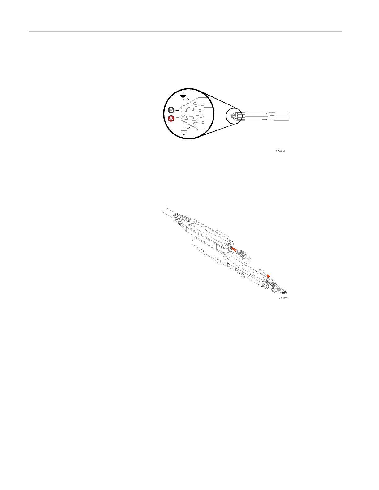
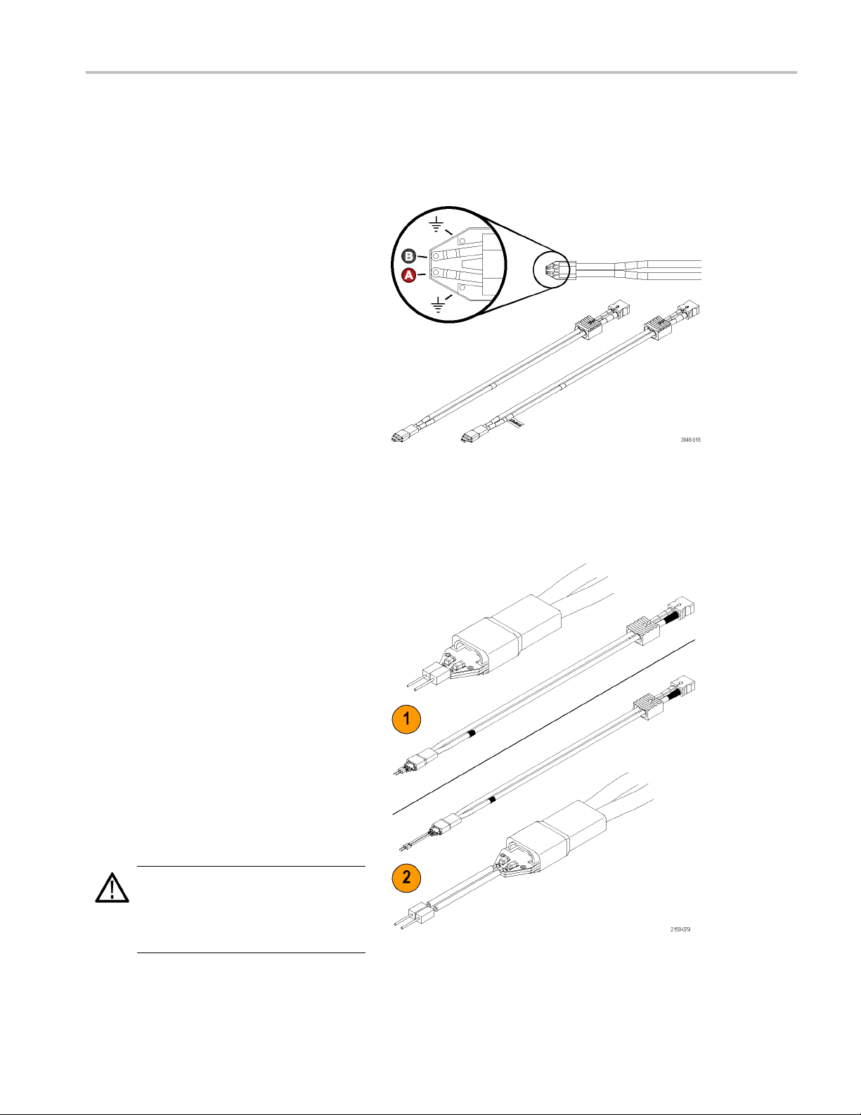
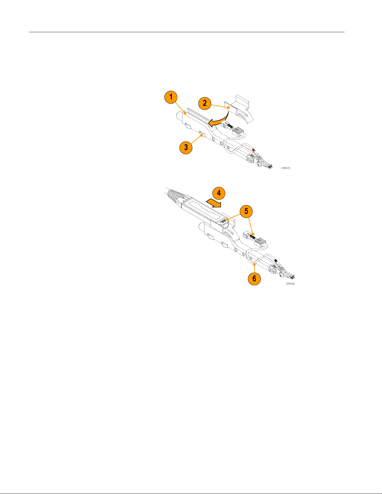
Connecting Accessories to the Probe Body
Installation
CAUTION. The p
when it is disconnected. To prevent damage to the probe, before you connect accessories to the probe body, always
check that the contacts are located in the probe body only.
The probe body and tip cable ends are keyed
to ensure correct installation. Connect them
as follows:
1. Orient the p
inputs on top, as shown.
2. Align the tip cable lead with the red band
to the A input.
3. Grasp the
push the cable into the probe body until
you feel a click. The cable housing is
fully sea
of the probe body.
4. To remove the tip, pull the cable tab
straight out from the probe body.
robe has replaceable contacts inside the probe body connector that may stick to the accessory connector
robe body with the A and B
cable connector by hand and
ted when it is flush with the edge
CAUTION
removing the tip. You may damage the tip or
probe if you pull on the cables.
. Pull only on the cable tab when
P7520A Probe Instruction M anual 5
Page 18
Installation
Control Box Controls and Indicators
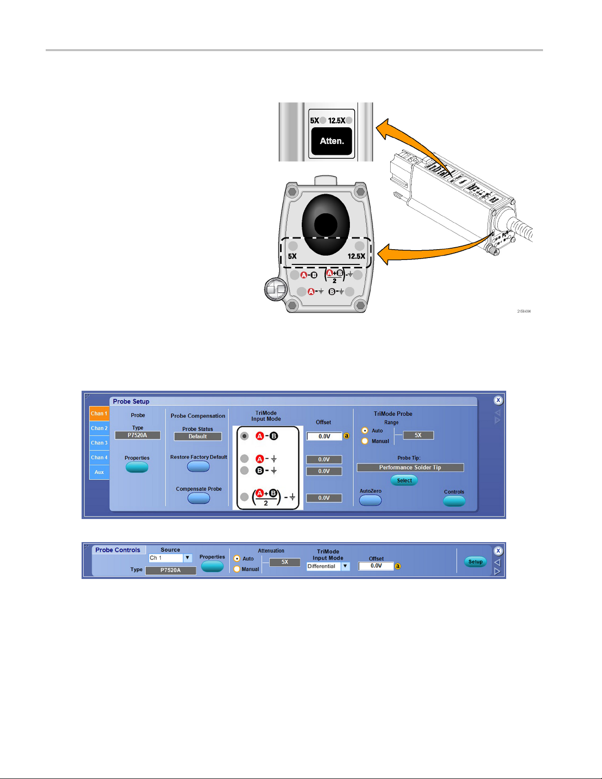
Atten. Button
After the probe is connected, the host
instrument automatically selects the
attenuation (voltage range) of the probe,
depending on the instrument volts/div setting.
You must change the attenuation autoselect
feature on the instrument to enable the
Atten. button on the probe:
1. In the oscilloscope menu bar, select
Vertical and then select Probe Setup.
2. From the Probe Setup or Probe Controls
screen, change the Range selection
from Auto to Manual. (See Figure 1
on page 6.) You can also change the
attenuation setting from these screens.
3. With the instrument in Manual Range
mode, press the Atten. button on
the probe to toggle the attenuation
setting between 5X and 12.5X. The
corresponding LED lights to indicate the
selected attenuation.
and LEDs
re 1: Probe Setup and Probe Controls screens
Figu
6 P7520A Probe Instruction Manual
Page 19

Input Mode Button and LEDs
Press the Input Mode button to s elect one of
the four TriMode measurements. The modes
cycle in the following sequence:
A – B (for differential signal
measurement)
A – GND (for A input single-ended
measurement)
B – GND (for B input single-ended
measurement)
(A + B)/2 – GND (for common mode
measurement)
NOTE. Some oscilloscope models only
allow the A – B Input Mode to be selected,
depending on which input tip is selected in
the oscilloscope Probe Setup screen. (See
page 71, Input Mode/Probe Tip Selection.)
Installation
The following pages discuss characteristics
of the TriMode measurements.
TriMode Probing
The TriMode feature allows you to view
two sing
differential waveform and common-mode
voltage without moving the probe connection.
Press t
the waveform views.
This example shows a typical HDMI signal
(one h
The resultant differential waveform and
common-mode voltage are shown.
le-ended signals and the resultant
he Input Mode button to cycle through
alf-lane) on the A and B inputs.
P7520A Probe Instruction M anual 7
Page 20
Installation
Connecting to Your Circuit
Before you connect these tips to your probe, we recommend that you perform a functional test and probe calibration.
(See page 9, Functional Check and Calibration.) Procedures for attaching the probe tips are described in Basic Operation.
(See page 16, Basic Operation.)
Use the P75TLRST Long Reach Solder Tip
to connect the probe to your circuit. The
P75TLRST Long Reach Solder Tip provides
a soldered, multi-point connection (A, B, and
GND). The P75TLRST tip is shipped with
the probe.
Use the optional P75P ST Performance
Solder Tip to get full bandwidth (>25 GHz)
measurements from the probe.
These tips provide full TriMode capabilities,
which are described in Basic Operation.
(See page 36, Input Mode Selection.)
Other tips are available and are described
later. (See page 30, Optional Accessories.)
The optional P75PDPM Precision Differential
Probing Module allows handheld and
fixtured probing of your circuit. The small,
precision-tapered tips and adjustable-width
tip spacing accommodate a variety of testing
needs.
The P75PDPM Probing Module is designed
for differential m easurements, and does not
incorporate a ground connection to your
circuit. However, you can make single-ended
measurements in the TriMode A – B mode by
connecting the B input to your circuit ground.
8 P7520A Probe Instruction Manual
Page 21
Functional Chec
k and Calibration
Functional Ch
After you connect the probe to the oscilloscope, perform a functional check using the calibration board included with the probe.
CAUTION. To avoid ESD damage to the probe, always use an antistatic wrist strap (provided with your probe), and work at a
static-approved workstation when you handle the probe.
Functional Check
This procedure checks the four TriMode settings on the probe, using the PROBE COMPENSATION or FAST EDGE
connection on the f
remaining input modes are checked and compared to the differential mode measurement.
Table 2: Required E
Item Description Performance Requirement Recommended Example
Oscilloscope TekConnect Interface Tektronix DPO/DSA72504D
Test board
Coaxial cable SMA, 50Ω, male-to-male
Coaxial cable BNC, 50Ω, male-to-male
1
Nine-digit part numbers (xxx-xxxx-xx) are Tektronix part numbers
2
Standard acces
sory included with probe
eck and Calibration
ront panel of the oscilloscope. The A – B (differential mode) is set up and verified first, and then the
quipment
1
TriMode DC Calibration board
067-1821-xx
174-1120-xx
012-0208-xx
2
2
2
P7520A Probe Instruction M anual 9
Page 22

Functional Chec
Test Setup
1. Connect the probe to any channel (1–4)
of the oscilloscope.
2. Set the oscilloscope to display the
channel.
3. Connect an SMA cable from the Probe
Compensation or FAST EDGE output
connector on the oscilloscope to the
SMA connector on the TriMode DC
Calibration board.
4. Set the two output switches on the
TriMode DC Calibration board to the
FAST RISE position.
5. Connect the probe to the cable on the
TriMode DC Calibration board (note
correct connector polarity).
k and Calibration
Test Procedure
6. Set the pr
the Input Mode to A – B.
7. Adjust the oscilloscope to display a
stable waveform (or press the Autoset
button)
NOTE. If you do not see a waveform, check
the connection at the probe body. (See
page 5, Co
Probe Body.)
8. When you see a stable square wave,
check t
cursors.) Signal output levels for some
oscilloscope models are listed below.
obe attenuation to 12.5X and
.
nnecting Accessories to the
he amplitude. (Use the horizontal
DPO/DSA72504D: 440 mV p-p
DPO/DSA73304D: 440 mV p-p
10 P7520A Probe Instruction M anual
Page 23

9. Cycle the Input Mode button through the
remaining selections and compare the
displayed wav
that you measured in step 8.
A – B (the waveform from step 8)
A – GND (same amplitude and
polarity as measured in step 8)
B – GND (the B input is grounded; no
signal is mea
eforms to the waveform
sured)
Functional Chec
k and Calibration
(A+B)/2 – GN
the same polarity as measured in
step 8)
10. Set the probe attenuation to 5X and the
Input Mode
11. Repeat ste
attenuation setting.
D (half-amplitude, but
to A – B.
ps 7 through 9 for the 5X
P7520A Probe Instruction M anual 11
Page 24

Functional Chec
k and Calibration
TriMode Probe Calibration
After you perform a functional check of the probe, run a probe calibration routine. We recommend that you repeat the probe
calibration for all four of the TriMode settings, and do this on each channel that you use.
The probe calibration operation minimizes measurement errors by optimizing the gain and offset of both probe attenuation
settings on each channel. Individual calibration constants are stored for each calibrated TriMode setting, on each probe, on
each channel.
CAUTION. To avoid ESD damage to the probe, always use an antistatic wrist strap ( provided with your probe), and work at a
static-approved workstation when you handle the probe.
You can use the equipment shown in the Functional Check to perform the probe calibration. (See Table 2 on page 9.)
12 P7520A Probe Instruction M anual
Page 25

Check the Instrument Calibration
Status
The Calibration Status of the instrument
Signal Path Compensation test must be
Pass for the probe calibration routine to run.
1. From the Utilities menu, select Instrument
Calibration.
2. In the Calibration box, check that the
Status field is Pass.
3. If the status is not pass, disconnect all
probes and signal sources from the
oscilloscope, and run the Signal Path
Compensation routine.
When the S ignal Path compensation test
status is Pass, calibrate the probe. (See
page 13, Calibrate the Probe.)
Calibrate t he Probe
Functional Chec
k and Calibration
1. Connect the probe to any channel (1–4)
of the oscilloscope. Allow the probe to
warm up fo
2. Set the o
channel.
3. Connect a BNC cable from the Probe
Calibration output connector on the
oscill
the TriMode DC Calibration board.
NOTE. You may be able to use the PROBE
COMPEN
your oscilloscope manual or online Help for
more information.
4. Connect the probe to the cable on the
TriMode DC Calibration board.
5. Set the Input Mode to A – B on the probe.
r 20 minutes.
scilloscope to display the
oscope to the BNC connector on
SATION output connector. Check
P7520A Probe Instruction M anual 13
Page 26
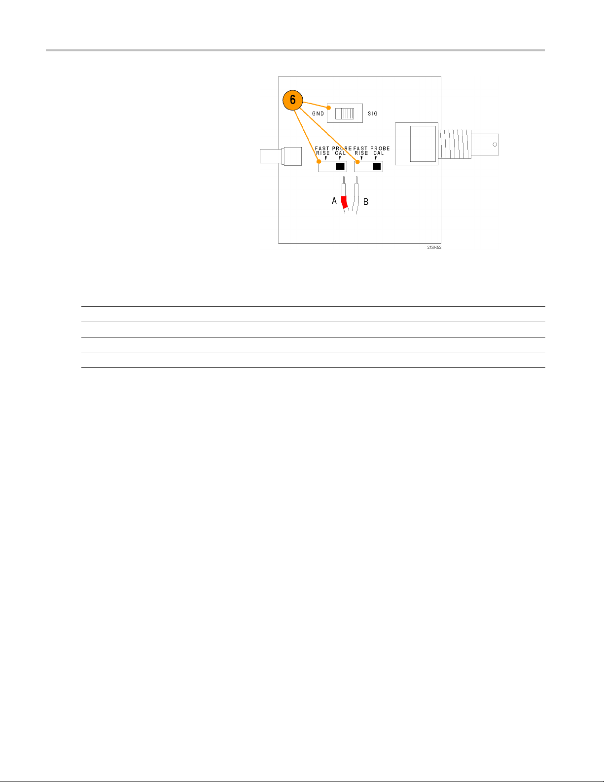
Functional Chec
6. Set the switches on the TriMode DC
Calibration board to the positions shown
for the select
Table 3.)
Table 3: TriMode DC Calibration board switch settings
k and Calibration
ed input mode. (See
Probe inpu
A–B
A
B
(A+B)/2 Probe Ca
tmode
Fast rise/
Probe Cal Gnd
Probe Cal Sig
Probe Ca
probe cal
l
l
Gnd/Sig
Sig
Sig
14 P7520A Probe Instruction M anual
Page 27
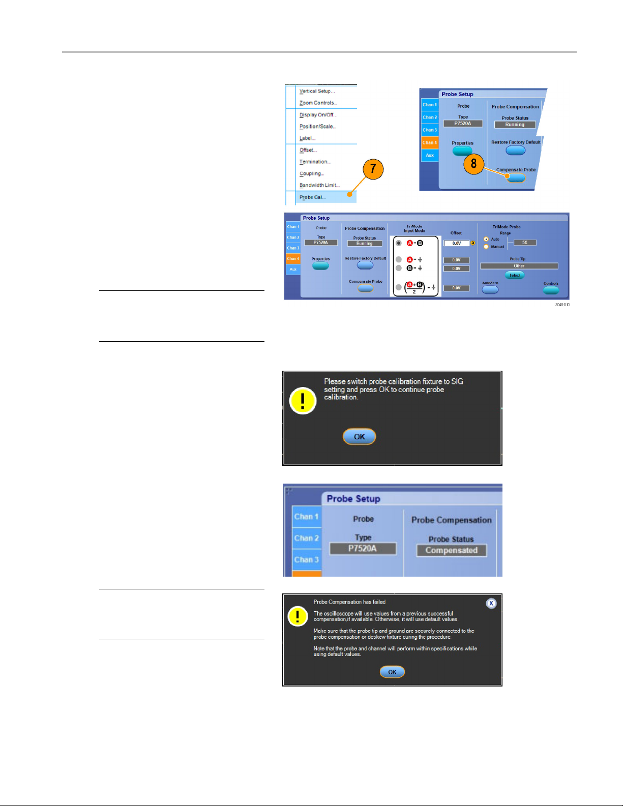
Functional Chec
k and Calibration
7. In the menu bar,
select Probe Cal.
The Probe Setup screen appears. (Some
oscilloscope
calibration routine and switch automatically
between input modes.)
8. Select Compensate Probe.
The probe cal
the probe to the oscilloscope for both probe
attenuation settings. The displayed results
differ betwe
9. Oscillosco
NOTE. If the Probe Cal routine fails, check
the connec
page 5, Connecting Accessories to the
Probe Body.)
10. Oscilloscopes that support the automated
s support an automated TriMode
en oscilloscope models:
automated TriMode calibration routine
display Compensated in the Probe
Status box.
the remaining input mode settings.
tion at the probe body. (See
TriMode calibration routine will display
an on-screen prompt to toggle the probe
calibration fixture SIG/GND switch.
Follow the instructions to complete the
calibration for the remaining input modes.
select Vertical and then
ibration routine runs, optimizing
pes that do not support the
Repeat steps 5 through 8 for
11. After a successful Probe Cal,
Compensated appears in the Probe
Status box.
NOTE. If the Probe Cal routine fails, check
the connection at the probe body. (See
page 5, Connecting Accessories to the
Probe Body.)
P7520A Probe Instruction M anual 15
Page 28

Basic Operation
Basic Operati
This section includes more information about using the probe controls on the control box and procedures for connecting
the probe to your circuit.
on
Maximizing P7520A Signal Bandwidth
The bandwidth of the P7520A probe can
be maximized to 25 GHz only when the
following conditions are met:
The host oscilloscope bandwidth must be
≥25 GHz and not be bandwidth limited.
The host oscilloscope sample rate must
be set to 100 GS/s. Slower sample rates
reduce the probe bandwidth.
The P7520A Input Mode must be set to
(A – B) mode. (Note: the bandwidth is
less for other input modes.)
A P75PST solder tip must be used for
the probe DUT connection.
The solder ramp that is supplied w ith the
probe is recommended as an aid to k eep
the probe tip wire connections as short
as possible (<0.032 in./0.8 mm).
16 P7520A Probe Instruction M anual
Page 29
Connecting to a Circuit Board
The P75TLRST Long Reach Solder Tip is shipped with the probe. Use the P75TLRST tip to connect the probe to your circuit,
or use the optional P75PST TriMode Performance Solder Tip for ≥25 GHz bandwidth measurements. Other TriMode solder
tips are available, as well as a handheld probing module, described on the following pages.
P75TLRST TriMode Long Reach
Solder Tip (Standard)
P75PST TriMode Performance
Solder Tip (Optional)
The Long Reach and Performance
Solder tips enable you to make full signal
characterizations from a m ulti-point soldered
connection.
The soldered connection passes the two
complementary signals (the A signal and the
B signal), and a ground reference from your
circuit to the TriMode probe.
The P75PST tip is optimized for high-speed
performance. Maximum P7520A bandwidth
can only be achieved with the P75PST
tip and an oscilloscope with ≥25 GHz
bandwidth.
Basic Operation
TriMode Resistor Solder Tips
These are optional accessory tips that you
can order for your probe. The tips provide
solder connection points for the A and B
probe input signals at the resistor leads,
instead of on the solder tip board.
1. 020-2936-xx TriMode Resistor Solder
Tip – measures <29 ps rise times
2. 020-2944-xx TriMode Extended Resistor
Solder Tip – measures <32 ps rise times
The tip resistors can tolerate more solder
cycles than the P75TLRST tip board, and
can be replaced when necessary.
These tips provide full TriMode capabilities
when you use the soldered-ground
connection on the tip board.
CAUTION. The TriMode solder tips are
very small and must be handled carefully to
avoid damaging them. The following pages
describe the proper techniques for using the
tips.
P7520A Probe Instruction M anual 17
Page 30
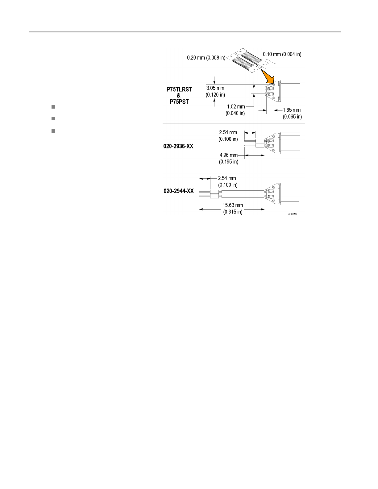
Basic Operation
The dimensions of the solder tip connections
are provided here for reference. You can
also design th
board layout for easier test connections.
To connect the probe tip to your circuit, use
the wire and so
wire replacement kit. The kit includes:
0.004 in (0.10 m m) wire
0.008 in (0.20 m m) wire
SAC305 solder (RoHS compliant)
You will also need tweezers, a low-wattage
soldering i
cutters.
Separate procedures follow for soldering the
different
e tip footprint into your circuit
lder that are provided in the
ron, and a pair of sharp wire
tips to your circuit.
18 P7520A Probe Instruction M anual
Page 31

Connect the P75TLRST or P75PST
Solder Tip
You must keep the interconnect wire lengths
short (<0.032 in./0.8 mm) to achieve 25 GHz
performance with the P75PST Solder Tip.
Use the solder tip ramp to position the
tip board close to the DUT test points to
minimize wire lengths.
1. Identify a location where the tip can be
placed, soldered, and secured to your
circuit.
NOTE. You can work with long wires
(~1 inch), but keep the finished wire lengths
of the signal and ground connections as
short as possible.
2. Lay the wires against a circuit board pad,
trace, or other conductive feature. (If
vias or through-holes are very close, you
can thread the wires through them.)
Basic Operation
3. Solder the wires to your circuit.
NOTE. For best results, use a flux pen to
clean your connections before soldering.
P7520A Probe Instruction M anual 19
Page 32

Basic Operation
4. Align the bottom of the tip to the notch in
the ramp as shown, and then secure the
tip to the ramp
The notch in the ramp helps you to
position the tip as close as possible
(<0.032 in./0
connections. Very short leads are
required for 25 GHz measurements.
5. Thread the wires through the tip.
6. Press the tip to the circuit board and
solder the w
finished wire lengths as short as possible.
7. Clip off the excess wire from all of the
solder joints.
8. Attach the probe to the tip. (Note
polarity)
with glue or tape.
.8 mm) to the circuit
ires to the tip. Keep all
.
9. For a secu
use tape or hot glue to secure the tip
and probe to your circuit. (See page 22,
Secure th
re mechanical connection,
eTip.)
Soldered Tip Example
The lead length of the connection wires
between the probe tip board and the DUT
must be k
the integrity of the measured signal.
The connection wires must also be kept as
equal i
skew between the A and B inputs.
This photo shows the P75PST solder tip
mounte
Typical wire lengths required for 25 GHz
performance are <0.032 in./0.8 mm.
Use a m
the best results. (See page 23, Notes on
Using the Tips.)
ept as short as possible to preserve
n length as possible to minimize the
d to the circuit with the solder ramp.
agnifying glass or m icroscope to get
20 P7520A Probe Instruction M anual
Page 33

Connect the TriMode Resistor
Solder Tips
Use this procedure to connect both styles of
resistor tips to your circuit.
1. Choose a location where the solder tip
resistor leads can reach your test points.
If you are using a ground connection,
note w hich solder tip ground via is
closest to your circuit ground.
2. Apply solder to the test points on your
circuit.
3. If you are not using the ground, solder
the resistor leads to your circuit, clip off
any excess, and go to step 11.
4. If you are using a ground wire, apply
solder to the solder tip ground via that
you chose.
5. Position a length of wire about 1-inch
long under the solder tip via.
Basic Operation
6. Heat the solder tip via and insert the wire.
7. Cut the excess wire on the other side of
the solder tip, flush with the board.
8. Cut the ground wire to the length required
to reach your circuit ground. Keep the
ground wire as short as possible to
ensure good performance.
9. Solder the ground wire to the circuit and
clip off any excess wire.
10. Solder the resistor leads to the test
points on your circuit and clip off any
excess leads.
P7520A Probe Instruction M anual 21
Page 34

Basic Operation
Secure the Tip
11. Push the end of the tip into the probe
head until it seats in the probe head.
12. For a secure mechanical connection,
use tape or hot glue to secure the tip to
your circuit.
13. Secure the probe to the circuit board with
tape or hook-and-loop strips.
22 P7520A Probe Instruction M anual
Page 35
Basic Operation
Notes on Using the Tips.
Use the following precautions when you solder the tips:
Use a low-wattage, temperature-controlled soldering iron and a small mass soldering iron tip. The soldering iron
temperature should be set as low as possible, while still providing a reliable solder joint.
Use SAC305 solder (included with the wire replacement kit) to attach the tip wires to the circuit under test.
The attachment wires should be bent symmetrically to vary the interconnect spacing. Use care when you solder a tip to a
circuit under test to avoid inadvertently desoldering either the attachment wires or the damping resistor.
For optimum performance and signal integrity, keep the lead length between the DUT (Device Under Test) and the tip as
short as possible, and the lead lengths the same length.
CAUTION. To prevent damage to the circuit board or circuit board connections due to accidental movement of the probe
and soldered leads, we recommend that you secure the tip to the circuit board using the adhesive tip tape provided in your
accessory kit. You can also use other materials such as Kapton tape or hot glue.
To avoid damage to the tip or the circuit under test, avoid applying excessive heat from the soldering iron. Use a low wattage,
temperature-controlled soldering iron and appropriately sized soldering iron tip.
P7520A Probe Instruction M anual 23
Page 36
Basic Operation
P75PDPM Precision Differential Probing Module (Handheld)
This is an opti
Optional Accessories.)
onal accessory. (See page 30,
Assemble the Module
1. Position the module housing as shown.
2. Slide the probing module handle adapter
into the module housing.
3. Secure the handle adapter with the
thumbscrew.
4. Insert the probe in the handle adapter.
5. Attach the cable to the probe body.
Match the red band to the A input.
6. You can dress the cable in the channels
as shown. The front channels are captive
and the rear channels are guides.
24 P7520A Probe Instruction M anual
Page 37
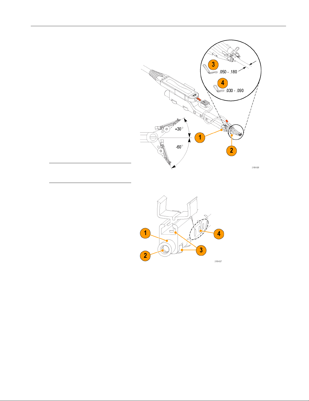
Adjustments
1. Adjust the tip angle by loosening the
setscrew and pivoting the tip. Tighten
the setscrew to secure the tip.
2. Adjust the tip spacing by turning the
adjustment wheel.
The probing module is shipped with a
ground spring installed between the tips.
The spring is necessary to pass the
highest-fidelity signal to your instrument.
The two available spring sizes are shown
in steps 3 and 4.
3. The large spring is pre-installed on the
probe and allows a tip-to-tip span from
0.050to0.180inches(1.27to4.57mm).
4. The small spring allows a tip-to-tip span
from 0.030 to 0.090 inches (0.76 to
2.28 mm).
NOTE. Spring replacement requires a
special tool. (See page 30, Optional
Accessories.)
Basic Operation
Mounting Features
You can mount the probing module to a
yoffixtures and custom probing arms,
variet
using the features described below:
1. The barrel at the rear of the P75PDPM
fits into the end of the PPM203B probe
r.
holde
2. The th
3. The slot below the barrel slides onto the
4. Use these threaded holes (6–32,
reads inside the barrel are metric
(M6 x 1), and attach to the EZ-Probe
Positioner from Cascade MicroTech.
f the PPM100 Probe Positioner.
tab o
Secure the module to the tab with the
thumbscrew.
, and 10–32) for custom-mount
8–32
applications.
P7520A Probe Instruction M anual 25
Page 38
Basic Operation
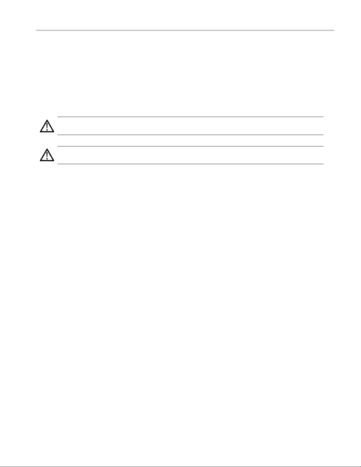
Connecting the Probe to Instruments without a TekConnect Interface
The 80A03 TekC
adapts any TekConnect probe to the
TDS8X00, CSA8X00, and DSA8200 Series
oscilloscope
The RTPA2A TekConnect Probe Interface
adapts any TekConnect probe to Tektronix
Real-Time Sp
NOTE. The 80A03 and RTPA 2A interfaces
are limited to a pass-through bandwidth of
18 GHz.
For proper
Interface firmware must be compatible with
the probe. (See page 70, Host Instrument
Firmware.
the rear panel of the 80A03 instrument.
The host instrument may also require a
firmware and/or operating system upgrade.
See your i
information.
onnect Probe Interface
s.
ectrum Analyzers.
probe operation, the Probe
)Thefirmware version label is on
nstrument manual for more
26 P7520A Probe Instruction M anual
Page 39

Accessories and
Options
Accessories a
You can reorder the following replacement parts and accessories. Note that in some cases, the reorder quantities may differ
from those that ship with the probe.
nd Options
Standard Accessories
The following accessories are shipped with the P7520A probe. If no quantity is listed, only one of that item is shipped.
Accessory
Reorder part number
and quantity Description
016-1997-xx Nylon carrying case with inserts. This carrying case has
several compartments to hold the probe and accessories.
006-3415-xx Antistatic wrist strap. When you use the probe, always
work at an antistatic work station and wear the antistatic
wrist strap.
--
---
071-3048-xx Instruction manual. The instruction manual provides
067-1821-xx
Calibration certificate. Acertificate of traceable calibration
is provided with every probe.
Data calibration report. The Data Calibration Report lists
the manufacturing test results of your probe at the time of
shipment and is included with every probe.
instructions for operating and maintaining the P7520A
TriMode probe.
TriMode DC calibration fixture. Use this fixture to perform
a functional check and a DC calibration with the host
instrument.
P7520A Probe Instruction M anual 27
Page 40

Accessories and
Accessory
Options
Reorder part number
and quantity Description
174-1120-xx
50 Ω SMA-M to SM
To perform a functional check, use this cable to connect
the DC Calibration fixture to the Fast Rise Time output
connector on t
A-M cable assembly, 8.5 in.
he host instrument.
012-0208-xx
020-3118of 25)
020-2729-xx
xx (package
50 Ω BNC-M to BNC-M cable assembly, 10 in.
To perform a probe calibration, use this cable to connect
the DC Calibration fixture to the DC Probe Cal output
connector on the host instrument.
Solder tip
These ramps help you to position the solder tips on your
circuit. Glue or tape a ramp to the bottom of the solder
tipsotha
your circuit connections (<0.032 in./0.8 mm for 25 GHz
measurements). The ramps work with all of the TriMode
solder ti
Accesso
accessories that are described below. A reference sheet
is included as a quick guide for using and reordering the
probe a
The foam insert includes slots for the optional P75PDPM
accessories that you can order.
ramp kit.
t the tip connections are as close as possible to
ps.
ry kit. The kit includes an assortment of
ccessories in the kit.
P75TLRST TriMode Long-Reach Solder Tip.
This tip provides a soldered, multi-point connection that
orts full TriMode measurement capabilities at full probe
supp
bandwidth.
Two tips are included with the probe.
006-8237-xx
(Strip of 10)
28 P7520A Probe Instruction M anual
Adhesive tip tape. Use the double-sided adhesive tip tape
to secure the solder tip assembly to your circuit board.
Page 41

Accessory
Reorder part number
and quantity Description
016-0633-xx
(Package of fiv
colored pairs)
020-2754(Package of 3 bobbins)
e
xx
Color band kit
pairs. When you are using more than one probe, the bands
enable you to visually match the probes to the channels
that they are c
To use the marker bands, attach one band to the indent
on the molded strain relief on the probe cable. Use the
matching col
control box.
Maintenance accessories listed below
Wire repla
SAC305 lead-free solder (RoHS compliant), 4 mil wire, and
8 mil wire. Use this kit to add wire leads on the solder tips.
Accessories and
. This kit includes two sets of five colored
onnected to.
or band on the other end of the probe, at the
cement kit. This kit includes three bobbins:
Options
013-0359-xx
(Package
003-1896-xx
of 4)
Replacement bullet contacts. To maintain the best
signal in
200 insertion cycles.
Bullet removal tool. This tool allows you to safely remove
and install the bullet contacts in the probe head.
tegrity, replace the bullets in the probe body after
P7520A Probe Instruction M anual 29
Page 42

Accessories and
Options
Optional Accessories
Optional accessory Part number Description
P75PST TriMode Performance Solder Tip.
This tip prov
supports full TriMode measurement capabilities at full probe
bandwidth.
ides a soldered, multi-point connection that
020-2936-
020-2944-xx
xx
TriMode Resistor Solder Tip kit.
This tip provides solder connection points at 100 Ω resistors
that exten
The resistors can withstand more solder cycles than the
P75TLRST and P75PST solder tips, and can be replaced
if they br
This tip can measure rise times down to <29 ps.
A kit of replacement resistors is available; see below.
TriMode
This tip provides solder connection points at 100 Ω resistors
that extend about 0.6 in (15 mm) from the solder tip board.
The res
P75TLRST and P75PST solder tips, and can be replaced
if they break.
This t
A kit of replacement resistors is available; see below.
d about 0.2 in (5 mm) from the solder tip board.
eak.
Extended Resistor Solder Tip kit.
istors can withstand more solder cycles than the
ip can measure rise times down to <32 ps.
30 P7520A Probe Instruction M anual
Page 43

Accessories and
Options
Optional acces
P75PDPM kit contents Part number Description
sory
Part number Description
020-2937-xx
P75PDPM Probing module kit.
Order P75PDPM kit
Replacement r
This kit includes:
100 Ω leaded resistors, quantity 50
75 Ω surface-mount, 0402 resistors, quantity 50
Nonconductive tubing, quantity 50
This kit allows you to browse multiple test points in your
circuit wit
The kit includes the parts listed under P75PDPM kit
contents below; some are also orderable separately.
Probing module.
The Probing Module includes the P7500 Tip Cable and a
large ground spring pre-attached to the tip pair, ready to
connect to your probe. To order the Probing Module, order
the P75PDPM kit.
hout using a soldered connection.
esistor kit for TriMode solder tips.
P75TC
P75PMT
367-0545-xx Probing module handle adapter.
P7500 tip cable. This cable connects the probe to the
Probing Module Tip. When the Probing Module kit is
ordered, the cable is shipped pre-installed on the Probing
Module.
To order the cable separately, order P75TC.
Probing module replacement tips (pair).
When the Probing Module kit is ordered, two sets of Probing
Module tip boards are shipped; one set is pre-installed on
the Probing Module. The replacement tips (one each left
and right) are built in pairs and must be separated before
installation.
To order the replacement tips separately, order P75PMT.
The Handle Adapter connects the probe body to the
handheld probing module.
P7520A Probe Instruction M anual 31
Page 44

Accessories and
P75PDPM kit contents Part number Description
Options
016-1998-xx
(Package of 4)
Ground spring kit, large.
The handheld p
ground connection between the ends of the two input tips.
Use the large ground spring for general-purpose browsing,
when the requi
0.180 in. (1.27 to 4.57 mm).
robing module requires a spring to make a
red span between tips is from 0.050 in. to
016-1999-xx
(Package of 4)
003-1900-
003-1897-xx
xx
Ground spring kit, small.
Use the small ground spring when you are probing dense
circuits an
confined area. The distance between the tips with the
small spring installed is from 0.030 in. to 0.090 in. (0.76
to 2.28 mm)
Ground spring tool.
This tool simplifies spring removal and installation. The
ends of th
the probe tips. A tab in the center of the tool is used to
set the span of the tips to the optimum width for spring
replace
Connect
Use this tool to disconnect the P7500 Tip Cable from the
Probing Module Tips. The tool protects the connectors and
tips fr
d where you may have multiple probes in a
.
e tool match the two springs that mount between
ment.
or separator tool.
om damage by gently spreading them apart.
32 P7520A Probe Instruction M anual
Page 45

Accessories and
Options
Optional acces
sory
Part number Description
067-1586-xx
PPM203B PPM203B Articulating Arm. This high-precision
PPM100 PPM100 Probe Positioner. This general-purpose benchtop
Deskew fixture
other probes connected to your measurement system.
articulati
axes. It is designed for probing circuit boards, hybrids,
and multi-chip modules (MCMs), that employ fine-pitch
devices an
provide stability and support for the probes when taking
measurements. Use the Probe Arm Adapter to attach a
probe to th
probe holder with flexible arm is designed for hands-free
probing that requires adjustable fine positioning. The heavy
duty base can be replaced with the clamp for securing the
probe arm in a variety of situations.
. Use this fixture to time-align the probe to
ng arm has fine adjustment controls for all three
d interconnects. Use the Articulating Arm to
e PPM203B Articulating Arm.
P7520A Probe Instruction M anual 33
Page 46

Accessories and
Options
Optional acces
sory
Part number Description
80A03
RTPA2A
80A03 TekConn
module with 80E0X Sampling Modules to adapt TekConnect
probes to TDS/CSA8000 and TDS/CSA8200 Series
Sampling Osci
NOTE. The 80A03 interface is limited to 18 GHz
pass-through bandwidth.
The interfac
compartment for one 80E0X Electrical Sampling Module
and two TekConnect probe inputs. The interface routes the
probe signa
panel. Semi-rigid SMA cables link the probe outputs to the
80E0X module inputs.
NOTE. The 8
or above to ensure full functionality with the P7520A probe.
RTPA2A TekConnect Probe Adapter. This adapter
allows you to connect a TekConnect probe to a Real-Time
Spectrum
NOTE. The RTPA2A interface is limited to 18 GHz
pass-through bandwidth.
The RTPA2A adapter firmware must be version 2.3 or
above to
Analyzer.
ensure full functionality with P7500 Series Probes.
ect Probe Interface Module. Use this
lloscopes.
e is composed of an enclosure that houses a
l outputs through SMA connectors on the front
0A03 adapter firmware must be version 2.3
Options
Option CA1. A single calibration event, or coverage for the designated calibration interval, whichever comes first.
Option C3. Calibration Service 3 years
Option C5. Calibration Service 5 y ears
Option D1. Calibration Data Report-ships standard with probe
Option D3. Calibration Data Report, 3 years (with Option C3)
Option D5. Calibration Data Report, 5 years (with Option C5)
Option G3. Gold Plan 3 years
Option G5. Gold Plan 5 years
Option R3. Repair Service 3 years
Option R5. Repair Service 5 years
-R3DW. Repair service coverage: 3 years (includes product warranty period), 3 year period starts at time of purchase.
-R5DW. Repair service coverage: 5 years (includes product warranty period), 5 year period starts at time of purchase.
34 P7520A Probe Instruction M anual
Page 47

Theory of Operat
ion
Theory of Oper
This section discusses operating considerations and probing techniques.
The P7520A probe is optimized for high bandwidth; it is not a general-purpose probe. The probe tips are miniaturized for
electrical characteristics and access to dense circuitry, and must be handled carefully.
CAUTION. To prevent damage to the probe, use care when handling the probe. Rough or careless use can damage the
probe.
ation
Attenuation and Input Mode Settings
Attenuation Selection
The Atten. (attenuation) button toggles the probe between the two nominal attenuation settings of 5X and 12.5X. The
choice of attenuation setting is a tradeoff between probe dynamic range and noise. The probe dynamic range represents
the operating range over which the probe is linear to within some specified percentage, such as ±1%. The probe noise is
usually specified as a noise spectral density and is significant because of the wide probe bandwidth. The 5X attenuation
setting provides the lowest noise performance. The 12.5X attenuation setting provides the largest dynamic range. The
actual probe attenuation factor is automatically accounted for by the attached oscilloscope using the intelligent TekConnect
probe interface. The attached oscilloscope also indicates the probe dynamic range with momentarily-displayed arrows when
the vertical channel controls are changed at larger vertical scale factor settings.
P7520A Probe Instruction M anual 35
Page 48

Theory of Operat
The usual choice for attenuation setting should be 5X, if the measured signal fits within the speci fied dynamic range, since
that provides t
DC bias and bring the displayed signal within the specified dynamic range. Although it is pos sible to measure signals that
exceed the dynamic range of the probe, the measured signal performance becomes increasingly non-linear and eventually
reaches a limi
not exceeded), the measured response no longer accurately represents the input signal.
Input Mode Selection
The Input Mode button toggles the internal probe input selector switches between the four input mode selections. This
TriMode feature allows full characterization of a differential signal from a single soldered connection.
A-B Mode. The A-B Mode is used for making differential signal m easurements and represents the traditional differential
probe functionality. Since the A-B Mode measures the difference between the A and B input signals, it eliminates any
common mod
For P7500 probe tips, such as the P75PDPM, which do not provide a TriMode ground reference, the A-B Mode is the only
useful mode for making low noise measurements. In fact, some oscilloscope models only allow the A-B Mode to be selected
when the co
measurements with the P75PDPM probe tip by connecting the B input to the local circuit ground.
A-GND Mode. The A-GND mode is used for making probe A input single-ended measurements with TriMode probe tips
such as the P75TLRS T and P75PST. These probe tips include a solder connection for the local circuit ground. In the A-GND
Mode the P7500 probe input switch is configured to measure the A input relative to this local circuit ground reference. The A
input signal measurement in A-GND Mode is designed for minimal coupling from any signal present on the B input within the
A input isolation performance of the probe.
ion
he best noise performance. The probe Offset control can also be used with some signals to compensate for a
ting level. Although probe signal limiting does not damage the probe (as long as the maximum input voltage is
e voltage, such as a DC bias common to both inputs, within the CMRR performance capability of the probe.
nnected tip does not include a ground reference. The A-B Mode can also be used for making single-ended
The A-GND Mode is not recommended for measurement use with the P75PDPM probe tip because of the lack of a local
circuit ground connection (and some oscilloscope models do not allow the A-GND Mode to be selected with the P75PDPM).
ode.
B-GND M
such as the P75TLRS T and P75PST. These probe tips include a solder connection for the local circuit ground. In the B-GND
Mode the P7500 probe input switch is configured to measure the B input relative to this local circuit ground reference. The B
signal measurement in B-GND Mode is designed for minimal coupling from any signal present on the A input within the
input
B input isolation performance of the probe.
Like the A-GND Mode, the B-GND Mode is also not recommended for measurement use with the P75PDPM probe tip
because of the lack of a local circuit ground connection.
The B-GND mode is used for making probe B input single-ended measurements with TriMode probe tips
(A+B)/2 Mode. The (A+B)/2 Mode is used for making common mode measurements on a differential signal and
represents a new probe feature that previously could only be made using oscilloscope math on multiple channels. For a
differential signal, the common mode measurement indicates the DC bias level and also shows the degree of asymmetry
between the A and B inputs. Since the (A+B)/2 Mode measures the average between the A and B input signals, it eliminates
any complementary differential signal voltage, within the DMRR performance capability of the probe.
36 P7520A Probe Instruction M anual
Page 49
Input Voltage Limits
The P7520A probe is designed to probe low-voltage circuits. Before probing a circuit, take into account the limits for
maximum input voltage, the operating voltage window, and the differential-mode signal range. (See Table 5 on page 52.)
Maximum Input Voltage
The maximum input voltage is the maximum voltage to ground that the inputs can withstand without damaging the probe
input circui
CAUTION. To avoid damaging the inputs of the probes, do not apply more than ±15 V (DC + peak AC) between each input
or between either probe input and ground.
try.
Theory of Operat
ion
CAUTION. To avoid E
static-approved workstation when you handle the probe.
SD damage to the probe, always use an antistatic wrist strap (provided with your probe), and work at a
P7520A Probe Instruction M anual 37
Page 50

Theory of Operat
Operating Voltage Window
The operating voltage window defines the maximum voltage that you can apply to each input, with respect to earth ground,
without saturating the probe input circuitry. (See Figure 2.) A common-mode voltage that exceeds the operating voltage
window may produce an erroneous output waveform even when the differential-mode specification is met.
Figure 2: Operating voltage window
ion
Differential-Mode Signal Range
The differential-mode signal range is the maximum voltage difference between the A and B inputs that the probe can accept
t distorting the signal. The distortion from a voltage that exceeds this maximum can result in a clipped or otherwise
withou
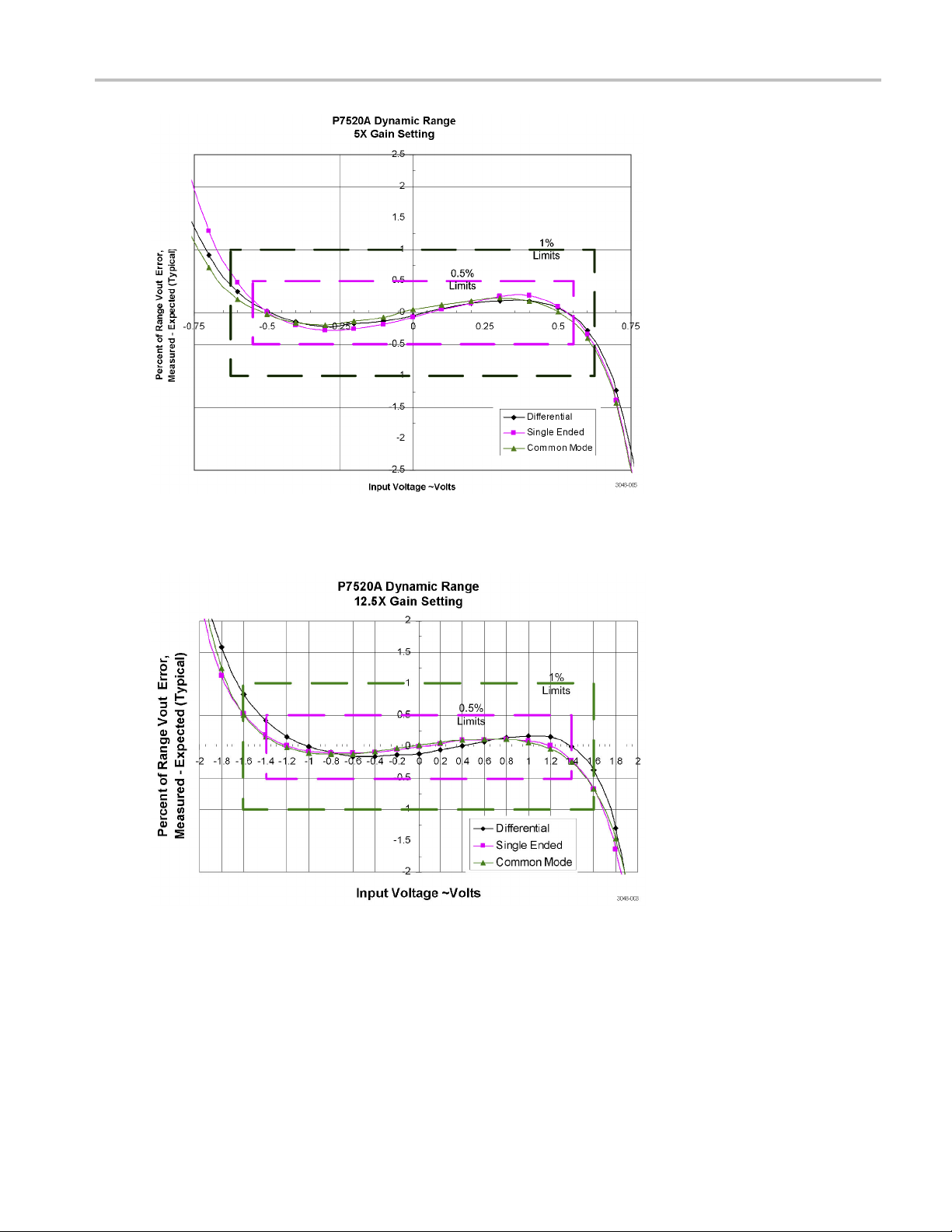
inaccurate measurement. The P7520A probe has two attenuation settings, 5 X and 12.5X, that allow dynamic range to be
traded off a gainst signal noise. The 12.5X attenuator setting has the largest dynamic range; the 5X attenuator setting has
est noise. T he graphs on the following pages illustrate the linearity error over the dynamic voltage range of the
the low
probes in both attenuation settings.
Offset Voltage Range
The Offset Voltage Control, accessible from the attached oscilloscope user interface, allows the probe dynamic range to
be effectively moved up and down within the limits of the offset voltage range and the operating voltage window. When
the offset voltage is set to zero volts and the input signal is zero volts (inputs shorted to ground, not open), the displayed
signal should be zero volts. If a noticeable zero volt offset is present under the above conditions, a Probe Cal operation
should be performed.
38 P7520A Probe Instruction M anual
Page 51
Theory of Operat
ion
Figure 3:
Figure 4: Dynamic range versus linearity, 12.5X range
Dynamic range versus linearity, 5X range
P7520A Probe Instruction M anual 39
Page 52

Theory of Operat
ion
TriMode Operation
The TriMode feature of the P7500 Series probe family is designed for improved convenience and enhanced capability in
measuring differential signal quality. Since a differential signal is composed of two com plementary single-ended signals,
full characterization of differential signal quality requires more than a simple differential measurement. A TriMode probe
features three Input Modes that allow a differential signal to be fully characterized with four measurements: differential,
positive polarity and negative polarity single-ended, and common m ode.
A TriMode probe provides improved efficiency and convenience by enabling full differential signal characterization from a
single soldered connection. Using one of the solder tips available for the TriMode probes, (for example, the P75TLRST
probe tip), probe connections are soldered to the two complementary si gnals (the A signal and the B signal) and a ground
reference. From this single DUT (device under test) connection, the internal electronic switching control of the TriMode
probe allows any one of the three probe Input Modes (four measurements) to be selected at a time. The TriMode probe
inputs are routed on the probe ASIC (application-specific integated circuit) to a set of four independent input amplifiers
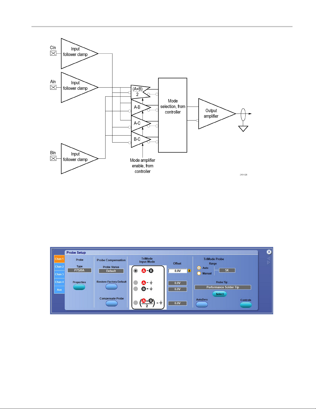
that perform the following signal calculations:
A – B (for differential signal measurement)
A – GND (for positive polarity single-ended measurement)
B – GND (for negative polarity single-ended measurement)
[A+B]/2 - GND (for common mode measurement)
NOTE. In the B – GND Mode, the negative polarity B input is not inverted.
The four input amplifiers are multiplexed together and only the selected Input Mode function is output to the connected
oscilloscope. (See Figure 5 on page 41.) The figure shows a conceptual view of the TriMode probe input structure, where
the C input provides the probe ground reference and is connected to the probe tip ground interconnect using the probe
tip cable coaxial shields.
40 P7520A Probe Instruction M anual
Page 53
Theory of Operat
ion
Figure 5: TriMode input structure
On oscilloscopes that do not provide full TriMode support, the TriMode features are controlled by the probe Control Box
switches, which allow oscilloscope features like Probe Cal to be exercised only for the selected probe Input Mode.
On oscilloscopes that provide full TriMode support, the oscilloscope-controlled probe GUI (graphical-user interface) can
perform a Probe Cal operation on all Input Modes and Attenuation Settings at once using the TriMode Probe Cal fixture
that is supplied with P7500 Series probes. Full TriMode support will also allow storage and automatic recall of relevant
settings like Offset. (See Figure 6.)
Figure 6: Typical TriMode Probe Setup screen
P7520A Probe Instruction M anual 41
Page 54
Theory of Operat
ion
Probing Techniques to Maximize Signal Fidelity
Signal fidelity is an indication of how accurately a probe represents the signal being measured. The signal fidelity of the
probe is best when the probe is applied properly to the circuit with the P7520A probe tips. Recommendations for c onnecting
the probe tips are given in the following section.
Probe Tip Cables and Connectors. Attached to the probe tip circuit board is a pair of very low skew (<1 ps) coaxial
cables and a p
enables quick and easy installation of the P75TLRST solder tip. The G3PO connector block of the probe tip is inserted into
the input nose piece on the end of the probe body of the P7500 family probes. The probe body contains a mating, polarized
G3PO connec
olarized G3PO dual connector block. The 3GPO connectors use a miniature, high frequency design that
tor block with attached G3PO connector bullets.
The connect
G3PO connectors. The G3PO connector in the probe body is designed to have higher detent force than the probe tip
connectors, which is intended to ensure that the G3PO bullets remain in the probe body connector when disconnected. The
probe body
the probe tip. The probe body nose springs also give a secure capture of the probe tip connector after insertion. Release of
the probe tip is assisted by using the wire-connected cable release holder on the probe tip connector. This probe tip release
holder sho
The follo
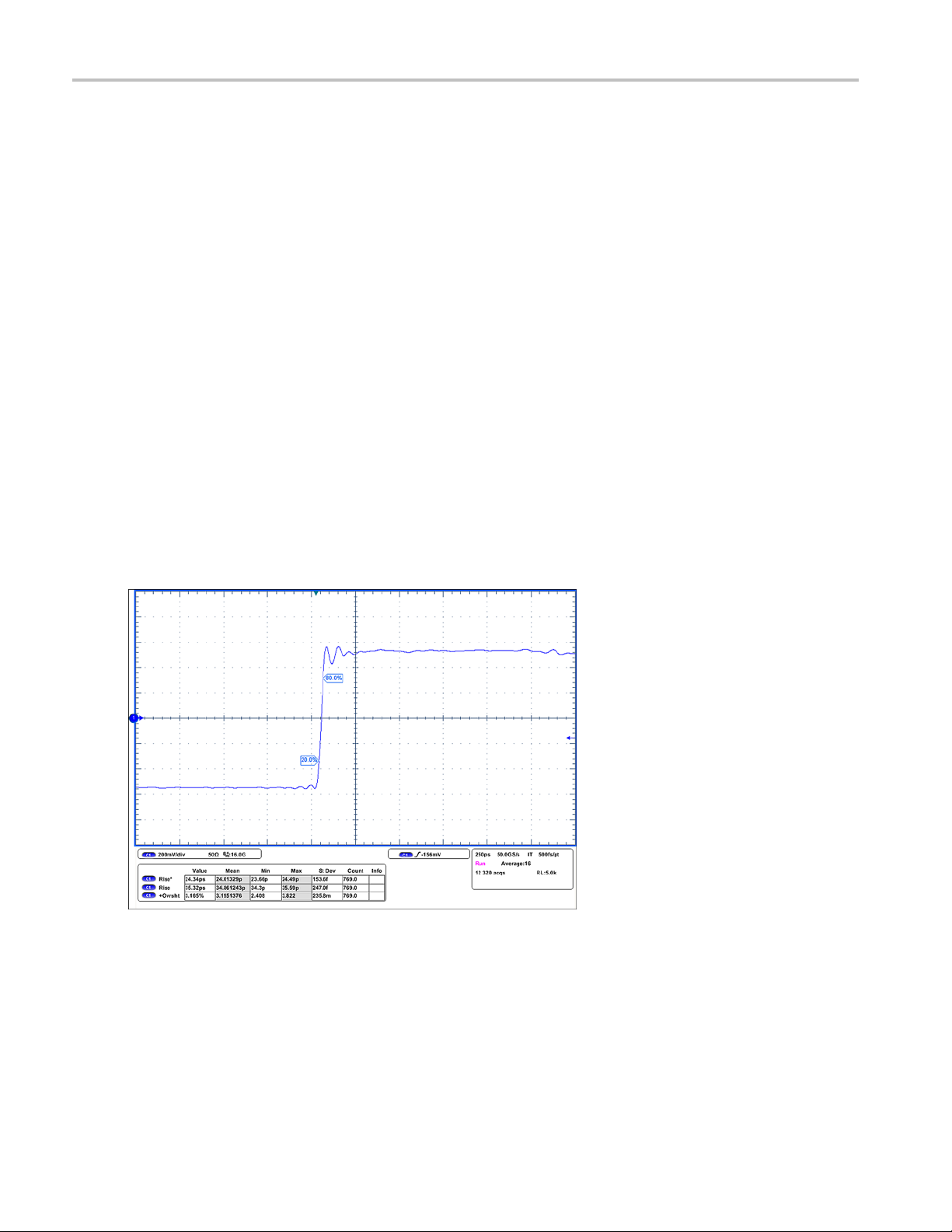
tip wire. Signal fidelity is best when the wire length is kept as short as possible. The step generator that was used as a
signal source for these screenshots has a 30 ps 10-90% rise time. The table in each figure contains data for two rise time
measurem
but actual results may vary depending on the other factors like characteristics of the device under test (for example, rise time
and impedance), precision of the solder c onnection, and the model of oscilloscope.
or bullets are a part of the G3PO connector design, providing a self-aligning interconnect mechanism between
nose piece, with its integral spring mechanism, helps to provide a self-aligning mechanism for hand insertion of
uld always be used rather than pulling on the probe tip cables, which may cause tip cable damage.
wing four figures illustrate the signal integrity effect on the P75TLRST solder tip when used with different lengths of
ents (10-90% and 20-80%). These screenshots can be used as a rough guide to gauge the effects of wire length,
Figure 7: P75TLRST solder tip with 0.010 in. of tip wire
42 P7520A Probe Instruction M anual
Page 55

Figure 8: P75TLRST solder tip w ith 0.050 in. of tip wire
Theory of Operat
ion
Figure 9: P75TLRST solder tip w ith 0.100 in. of tip wire
P7520A Probe Instruction M anual 43
Page 56

Theory of Operat
Figure 10: P75TLRST solder tip with 0.200 in. of tip wire
ion
44 P7520A Probe Instruction M anual
Page 57
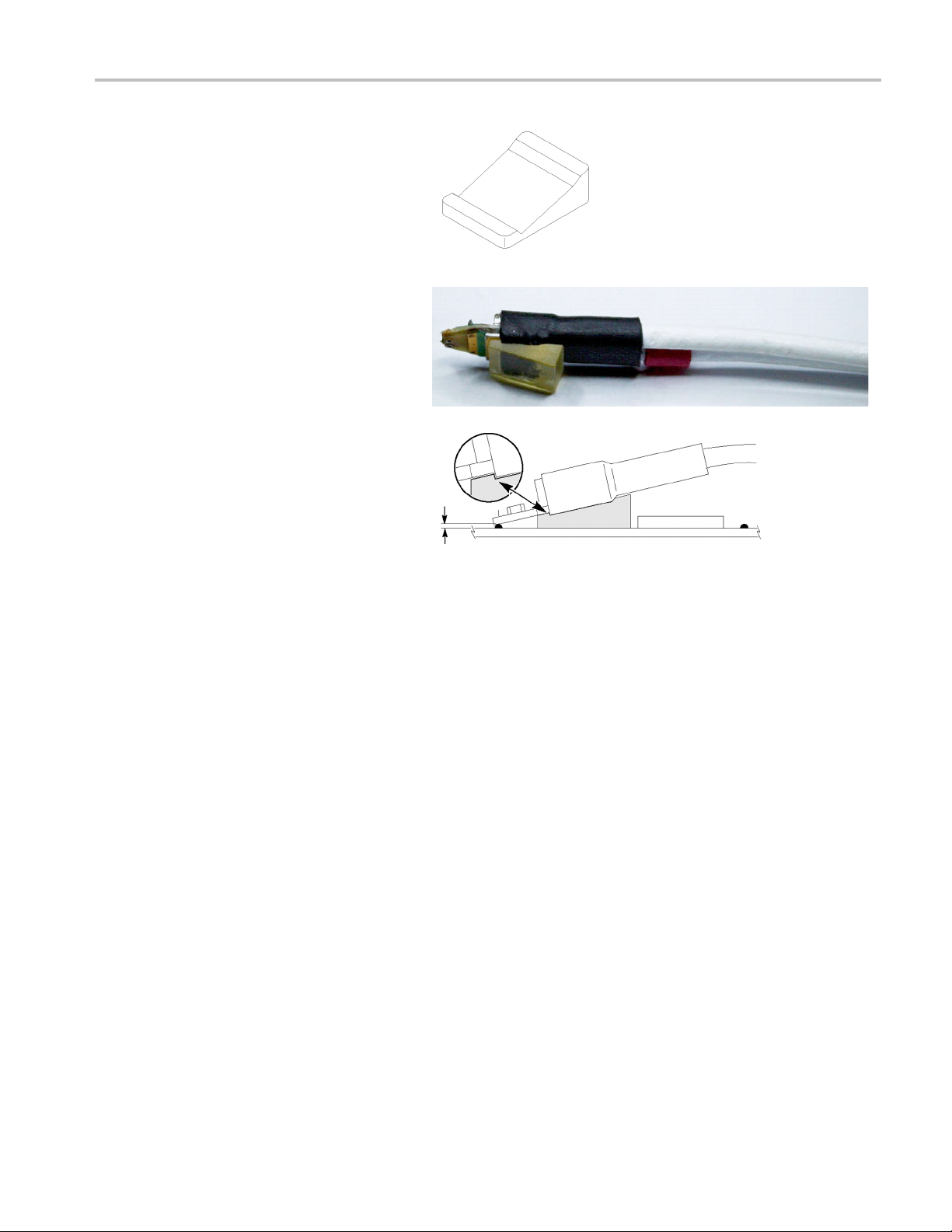
Solder Tip Ramp
For best performance, the solder tip must
be placed very close to the circuit (within
0.032 in./0.8 mm). The solder tip ramp is
designed to hold the solder tips 0.025 in.
(0.6 mm) away from your circuit c onnections.
Align the body of the tip to the notch in the
ramp as shown. This alignment to the notch
ensures the tip-to-circuit gap is 0.025 in.
(0.6 mm). Glue or tape the tip to the ramp.
Thread the soldered wires from your circuit
test point through the vias on the tip. Glue or
tape the t
the wires from your circuit to the tip.
ip to your circuit, and then solder
Theory of Operat
ion
P7520A Probe Instruction M anual 45
Page 58

Theory of Operat
P75PDPM Precision Differential Probing Module
The P75PDPM Probing Module is designed for handheld and fixtured probing applications. The P75PDPM probe tip is
composed of two replaceable probe tip circuit boards with a pin on one end and a G3PO socket connector on the other.
Damping resistors on the tip boards near the input pins and a 50 Ω transmission line on the board transmit the signal from
the input pin to the G3PO socket connector. The probe tip boards are connected to the P7500 probe body with a very
low skew (<1 ps) cable assembly (P75TC).
The left-side and right-side probe tip boards mount at an angle in the P75PDPM adjustment housing. The probe tip spacing
is adjustable from 0.030 – 0.180 in. (0.76 – 4.57 mm) using the thumb-operated screw. Because of the variable spacing
between the two probe tip boards, a gold-plated ground spring is connected between the probe tip boards to ensure a
good common mode ground return near the probe tip pins.
ion
Figure 1
The P75PDPM probe tip circuit boards mount in an articulating metal housing that also supports the variable spacing control.
The angle of the probe tip housing can be adjusted and locked in place using an articulation screw in the probe holder bar.
The probe holder bar contains mechanical details for retaining the probe tip cable assembly as well as a retaining clamp
for the probe body. The probe holder bar can be held manually or can be mounted for fixtured probing on an articulating
probe arm using mechanical features in the holder bar.
The P75PDPM design features improved mechanical compliance in probe tip attachment to the DUT. Mechanical compliance
is a significant issue for differential probes because of the difficulty in making reliable contact with two DUT connections at
the same time. The reliability in making this dual point connection can be improved by a tip structure with good mechanical
compliance, in which there is sufficient give in the probe tips to absorb interconnect surface irregularity.
The P75PDPM does not have a local DUT ground connection because of the great difficulty in making a good three-point
interconnect without soldering. As a result, the only low-noise TriMode Input Mode available with the P75PDPM is the A-B
(DIFF) mode, since for differential signals, there is an inherent virtual ground present in the measurement circuit.
The following four figures illustrate the signal integrity effect of changing the spacing on the P75PDPM Probing Module.
Signal fidelity is best with the tips at the smallest spacing. The step generator that was used as a signal source for these
screen shots has a 30ps 10-90% rise time. The table in each figure contains data for two rise time measurements (10-90%
and 20-80%). These screen shots can be used as a rough guide to gauge the effects of probe tip spacing, but actual
results may vary depending on the other factors like characte ristics of the device under test (for example, rise time and
impedance) and the model of oscilloscope.
1: P75PDPM Precision Differential Probing Module
46 P7520A Probe Instruction M anual
Page 59
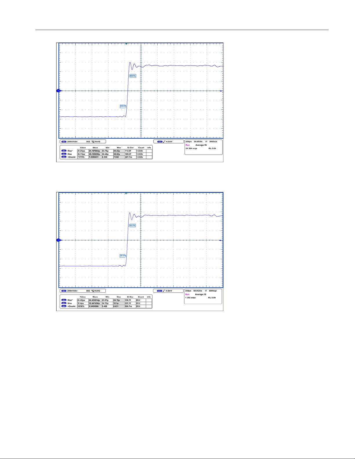
Figure 12: P75PDPM with short ground spring, 0.030 in. spacing
Theory of Operat
ion
Figure 13: P75PDPM with short ground spring, 0.050 in. spacing
P7520A Probe Instruction M anual 47
Page 60

Theory of Operat
Figure 14: P75PDPM with short ground spring, 0.090 in. spacing
ion
Figure 15: P75PDPM with short ground spring, 0.180 in. spacing
48 P7520A Probe Instruction M anual
Page 61

Input Impedance and Probe Loading
When you connect the probe inputs to a circuit, you are introducing a new resistance, capacitance, and inductance into the
circuit. Each input of the differential probe has a DC input impedance of 50 kΩ to ground. (See Figure 16.)
Figure 16: TriMode probe input model
For signals with low source impedance and frequency, the 50 kΩ input impedance on each input is large enough to prevent
the inputs from loading the signal sources. The more the signal source impedance on an input increases, the more the
probe loads the source and reduces the signal amplitude. The greater the source impedances and the higher the signal
frequencies, the more you must take these factors into account.
Theory of Operat
ion
The frequency of the signal also affects signal measurement. As the frequency of the signal increases, the input impedance of
the probe decreases. The lower the impedance of the probe relative to that of the source, the more the probe loads the circuit
under test and reduces the signal amplitude. A high frequency input impedance model is shown below. (See Figure 17.)
e 17: TriMode probe high frequency input impedance model
Figur
For plots and representative R-L-C values of the individual TriMode solder tips, refer to the specifications. (See page 56,
Tip Specifications.)
P7520A Probe Instruction M anual 49
Page 62

Theory of Operat
Embedded Probe
It is possible to acquire signals with the P7500 Series TriMode probes by including an embedded connection in your
circuit. (See Figure 18.) Connectors that mate to the P75TC Tip Cable can be incorporated in the circuit board design and
carefully placed to balance any reflections or other characteristics that may affect the circuit or measurement. An embedded
probe connection will generally provide optimum probe performance because the signal interconnect lead length can
be minimized if implemented correctly. For more information about embedded probe connections, contact Tektronix.
(See page , Contacting Tektronix.)
ion
Figure 18: Embedded probe fixture
50 P7520A Probe Instruction M anual
Page 63

Specifications
Specification
These specifications apply to the P7520A TriMode Probe when it is installed on an oscilloscope that has the supporting
firmware, DSP capabilities, and a TekConnect interface. The probe must have a warm-up period of at least 20 minutes and
be in an environment that does not exceed the allowed limits. (See Table 1.)
Specifications for the P7520A TriMode Probe fall into three categories: warranted, typical, and nominal characteristics.
s
Warranted Characteristics
Warranted c
Table 4: Warranted electrical characteristics
Character
DC attenua
Output Offset Zero ±3 mV (+20 to +30 °C, +68 to +86 °F) (5X) ±15 mV
Tempera
Humidity
Altitude
haracteristics describe guaranteed performance within tolerance limits or certain type-tested requirements.
istic
tion accuracy
ture
Specificat
0.200 ±2% (
0.0800 ±2% (12.5X)
on oscilloscope
±3 mV (+2
±37.5 mV on oscilloscope
Operating: 0 to +40 °C (+32 to +104 °F),
Nonoperating: –20 to +71 °C (-4 to +160 °F)
Operating: 20–80% RH, at up to +40 °C (+104 °F)
Nonop
Opera
Nonoperating: 12,000 meters (40,000 feet)
ion
5X)
0 to +30 °C, +68 to +86 °F) (12.5X)
erating: 5–90% RH
ting: 3000 meters (10,000 feet)
P7520A Probe Instruction M anual 51
Page 64

Specifications
Typical Characteristics
Typical characteristics describe typical, but not guaranteed performance w ith an embedded probe only. Refer to Tip
Specifications for specifications when using TriMode accessory tips. Highest performance is achieved when using the
P75PST tip with the probe. (See page 56, Tip Specifications.)
Table 5 : Typical electrical characteristics
Characteristic Specification
Bandwidth (DSP corrected)
Rise time
Operating voltage window
Differential signal range (DC
coupled)
Linearity
Offset voltage range
input)
DC offset drift ( referred to input)
DC voltage measurement accuracy
Maximum nondestructive input voltage
Input impedance
Differential input resistance, DC coupled 100 kΩ ±6 kΩ
Input resistance matching
Common-mode input resistance,
DC coupled
1
10–90% <20 ps, differential mode, 100 GS/s
20–80%
5X ±0.625 V
12.5X ±1.60 V
5X
12.5X
Differential
Single-ended and
common-mode
Differential 0.093 ±2%, referred to inputOffset scale accuracy (referred to
Single-ended and
common-mode
Differential –0.100 μV/ °C (5X)
Single-ended and
common-mode
5X
12.5X
≥25 GHz, differential mode, 100 GS/s
≥23 GHz, differential mode, 50 GS/s
≥18 GHz, A, B, and common modes
<23.5 ps, differential mode, 50 GS/s
<29 ps, A, B, and common modes
<18ps,A–Bmode
<20 ps, other modes
-2.0 V to +3.7 V
±1% over a dynamic range of –0.625 V to
+0.625 V
±1% over a dynamic range of –1.60 V to
+1.60 V
–1.5 V to +2.5 V
–1.8 V to +3.4 V
0.186 ±2%, referred to input
–0.60 μV/ °C (12.5X)
+0.100 μV/ °C (5X)
+0.30 μV/ °C (12.5X)
±(2% of input + 2% of offset + 15 mV +
6.25 mV)
±(2% of input + 2% of offset + 37.5 mV +
16 mV)
±15 V (DC + peak AC) between each input or
between either probe inputs and ground
(See page 29, Tip Specifications.)
±250 Ω side-to-side with respect to ground
50 kΩ ±3 kΩ
52 P7520A Probe Instruction M anual
Page 65
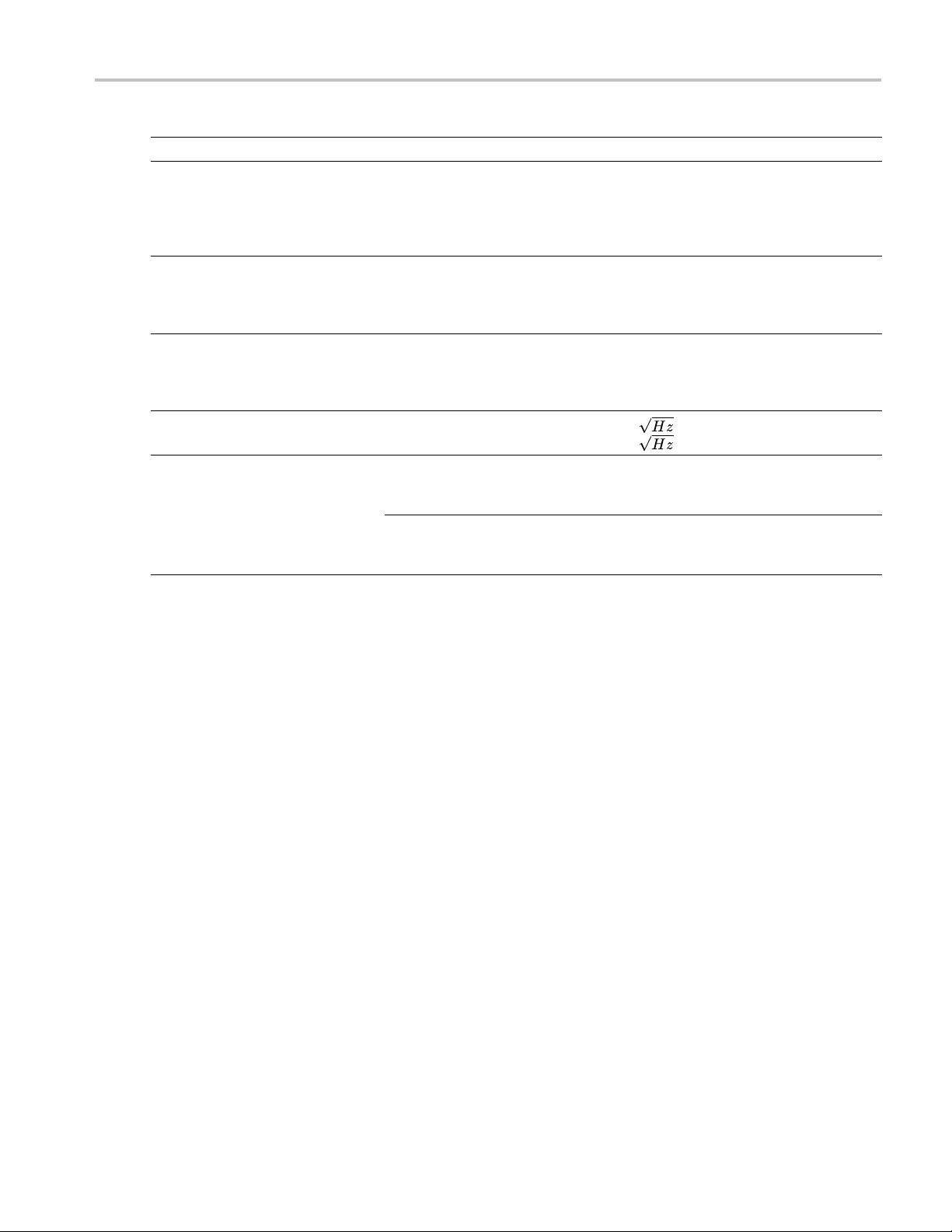
Specifications
Characteristi
c
Specification
Delay time 4.4 ns ±0.1 ns
Common-mode rejection ratio, differential-mode
2
>60 dB at DC
>40dBto50MHz
>30dBto1GHz
>20dBto10GHz
z
z
Differenti
al-mode rejection ratio, common-mode
>12dBto20GH
2
>40dBto50MHz
>30dBto1GH
>20dBto9GHz
>12dBto18GHz
Channel isolation, single-ended mode
2
>40dBto50MHz
>30dBto1GHz
>15dBto9G
Hz
>6 dB to 18 GHz
Noise, probe only (all modes)
<33 nV/
<48 nV/
System noise
1
5X
20 GHz: 4.6 mV
23 GHz, 50 GS/s: 5.2 mV
25 GHz, 100 GS/s: 6.2 mV
12.5X
20 GHz: 8.9 mV
23 GHz, 50 GS/s: 10.0 mV
25 GHz, 100 GS/s: 12.5 mV
1
Measured using a ≥25 GHz oscilloscope @100 GS/s and a P75PST solder tip. The probe input mode is set to A-B (differential).
2
Embedded probe only. Refer to Tip Specifications for specifications when using TriMode accessory tips. (See page 90, Tip Specifications.)
(5X)
(12.5X)
RMS
RMS
RMS
RMS
RMS
RMS
P7520A Probe Instruction M anual 53
Page 66

Specifications
Table 6 : Typical mechanical characteristics
Characteristi
Dimensions, control box
Dimensions, probe body
Dimensions, cable length
Unit weight
Figure
c
19: Probe body and co ntro l box dimensions
Description
125.4 mm × 41 mm
101.6 mm × 8.8
1.0 m (39.3 in
1.550 g (3.1
9 mm × 19 mm (4.0 in × 0.350 in × 0.750 in)
) (from the probe body to the control box)
lbs) (probe, accessories and packaging)
×35mm(4.9in×1.6in×1.4in)
54 P7520A Probe Instruction M anual
Page 67

Nominal Characteristics
Nominal characteristics describe guaranteed traits, but the traits do not have tolerance limits.
Table 7: Nominal electrical characteristics
Characteristic Description
Input configuration
Output coupling DC
Probe attenuation
settings
P75PST solder tip
P75TLRST solder tip
TriMode Resistor & Extended
Resistor solder tips
P75PDPM handheld module
Specifications
Differential (two signal inputs, A and B; shared with single-ended)
Single-ended (one each A and B signal input and two ground
inputs)
Differential (two inputs, A and B)
5X and 12.5X
P7520A Probe Instruction M anual 55
Page 68

Specifications
Tip Specifications
This section lists specifications that are applicable to the probe when used with the accessory tips available for the probe.
All solder tips must be connected to the circuit with the shortest leads possible (typically <0.032 in./0.8 mm). Solder ramp
accessories are included with the probe to help you minimize the lead lengths. The solder ramps position the probe tip
connections as close as possible to your circuit test points.
56 P7520A Probe Instruction M anual
Page 69
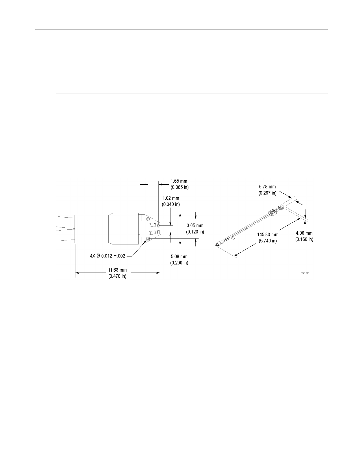
Specifications
P75PST Performance Solder Tip
Specifications are typical and apply to all ranges and input modes unless specified otherwise. To achieve the h ighest
performance in differential (A–B) mode, the host instrument bandwidth must be ≥25 GHz with a sample rate of 100 GS/s.
The soldered wires between the tip and your circuit must be kept as short as possible (typically <0.032 in./0.8 mm). The
bandwidth is less than 25 GHz for the other m easurement modes (A, B, and common mode).
Bandwidth Rise time CMRR DMRR Channel isolation
>25 GHz, A–B
mode, 100 GS/s
≥23 GHz, A–B
mode, 50 GS/s
>18 GHz,
A, B, CM modes
10%–90%:
<20 ps, A–B mode,
100 GS/s
<23.5 ps, A–B mode,
50 GS/s
<29 ps, A, B, CM
modes
20%–80%:
<15 ps, A–B mode
<20 ps, A, B, CM
modes
>60 dB at DC
>40 dB at 50 MHz
>30 dB at 1 GHz
>20dBat10GHz
>12dBat20GHz
>40dBat50MHz
>30 dB at 1 GHz
>20 dB at 9 GHz
>15dBat18GHz
>40dBat50MHz
>30 dB at 1 GHz
>15 dB at 9 GHz
>6 dB at 18 GHz
Figure 20: P75PST Performance Solder Tip dimensions
P7520A Probe Instruction M anual 57
Page 70

Specifications
The following figure shows the typical step response of the probe with the P75PST solder tip. A 25 ps rise time pulse source
was used for thi
s measurement.
Figure 21: TriMode probe with the P75PST solder tip
58 P7520A Probe Instruction M anual
Page 71

The following figure shows a typical impedance plot of the probe with the P75PST solder tip.
Figure 22: P75PST differential impedance
Specifications
P75TLRST TriMode Long Reach Solder Tip
Bandwidth Rise time CMRR DMRR Channel isolation
>20 GHz, A–B mode
>18GHz,A,B,CM
modes
10%–90%:
<27 ps, A–B mode
<29 ps, A, B, CM
modes
20%–80%:
<18 ps, A–B mode
<20 ps, A, B, CM
modes
>60 dB at DC
>40 dB at 50 MHz
>30 dB at 1 GHz
>20dBat10GHz
>15dBat20GHz
>40dBat50MHz
>30 dB at 1 GHz
>20 dB at 9 GHz
>15dBat18GHz
>40dBat50MHz
>30 dB at 1 GHz
>15 dB at 9 GHz
>6 dB at 18 GHz
P7520A Probe Instruction M anual 59
Page 72

Specifications
Figure 23: P75TLRST TriMode Long Reach Solder Tip dimensions
60 P7520A Probe Instruction M anual
Page 73
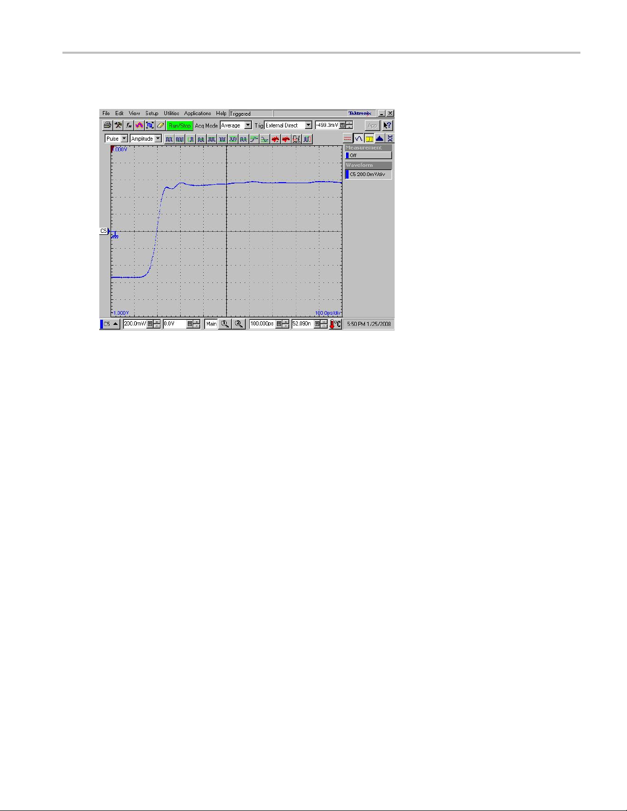
Specifications
The following figure shows the typical step response of the probe with the P75TLRST solder tip. A 50 ps rise time pulse
source was used
for this measurement.
Figure 24: TriMode probe with the P75TLRST solder tip
P7520A Probe Instruction M anual 61
Page 74

Specifications
The following figure shows a typical impedance plot of the probe with the P75TLRST solder tip.
Figure 25: P75TLRST differential impedance
62 P7520A Probe Instruction M anual
Page 75

Specifications
TriMode Resistor Solder Tip
Specifications are typical and apply to all ranges and input modes unless specified otherwise.
Bandwidth Rise time CMRR DMRR Channel isolation
>18.0 GHz, A–B
mode
>15.0 GHz, A, B
modes
>12.0 GHz, CM
mode
10%–90%:
<29 ps, A–B mode
<32 ps, A, B
modes
<34 ps, CM mode
20%–80%:
<20 ps, A–B mode
<22 ps, A, B
modes
<24 ps, CM mode
>60 dB at DC
>40dBat50MHz
>30 dB at 1 GHz
>20 dB at 10 GHz
>15 dB at 20 GHz
>40dBat50MHz
>30 dB at 1 GHz
>20 dB at 9 GHz
>15dBat18GHz
>40dBat50MHz
>30 dB at 1 GHz
>15 dB at 9 GHz
>10dBat18GHz
Figure 26: TriMode Resistor solder tip dimensions
P7520A Probe Instruction M anual 63
Page 76

Specifications
The following figure shows the typical step response of the probe with the TriMode resistor solder tip. A 50 ps rise time
pulse source wa
s used for this measurement.
Figure 27: Step response with the TriMode Resistor solder tip
owing figure shows a typical impedance plot of the probe with the TriMode resistor solder tip.
The foll
Figure 28: TriMode Resistor solder tip differential impedance
64 P7520A Probe Instruction M anual
Page 77

Specifications
TriMode Extended Resistor Solder Tip
Specifications are typical and apply to all ranges and input modes unless specified otherwise.
Bandwidth Rise time CMRR DMRR Channel isolation
>7 GHz, A–B
mode
>4 GHz, A, B
modes
>2.5 GHz, CM
mode
10%–90%:
<32 ps, A–B mode
<50 ps, A, B
modes
<120 ps, CM
mode
20%–80%:
<24 ps, A–B mode
<30 ps, A, B
modes
<40 ps, CM mode
>60 dB at DC
>40dBat50MHz
>30 dB at 1 GHz
>20dBat10GHz
>15dBat20GHz
>40dBat50MHz
>30 dB at 1 GHz
>20 dB at 9 GHz
>15dBat18GHz
>40 dB at 50 MHz
>30 dB at 1 GHz
>15 dB at 9 GHz
>10 dB at 18 GHz
29: TriMode Extended Resistor solder tip dimensions
Figure
P7520A Probe Instruction M anual 65
Page 78

Specifications
The following figure shows the typical step response of the probe with the TriMode extended resistor solder tip. A 50 ps
rise time pulse
source was used for this measurement.
Figure 30: Step response with the TriMode Extended Resistor solder tip
owing figure shows a typical impedance plot of the probe with the TriMode extended resistor solder tip. The L=0
The foll
value gives a simplifi ed model that follows the lower impedance limit envelope.
ure 31: TriMode Extended Resistor solder tip differential impedance
Fig
66 P7520A Probe Instruction M anual
Page 79

P75PDPM Precision Differential Prob ing Module
Specifications are typical and apply to all ranges and input modes unless specified otherwise.
Bandwidth Rise time CMRR
>18.0 GHz 10%–90%: <29 ps
20%–80%: <20 ps
>60 dB at DC
>40dBat50MHz
>30dBat1GHz
>20dBat10GHz
>15dBat20GHz
Specifications
Figure 32: P75PDPM Precision Probing Module dimensions
P7520A Probe Instruction M anual 67
Page 80
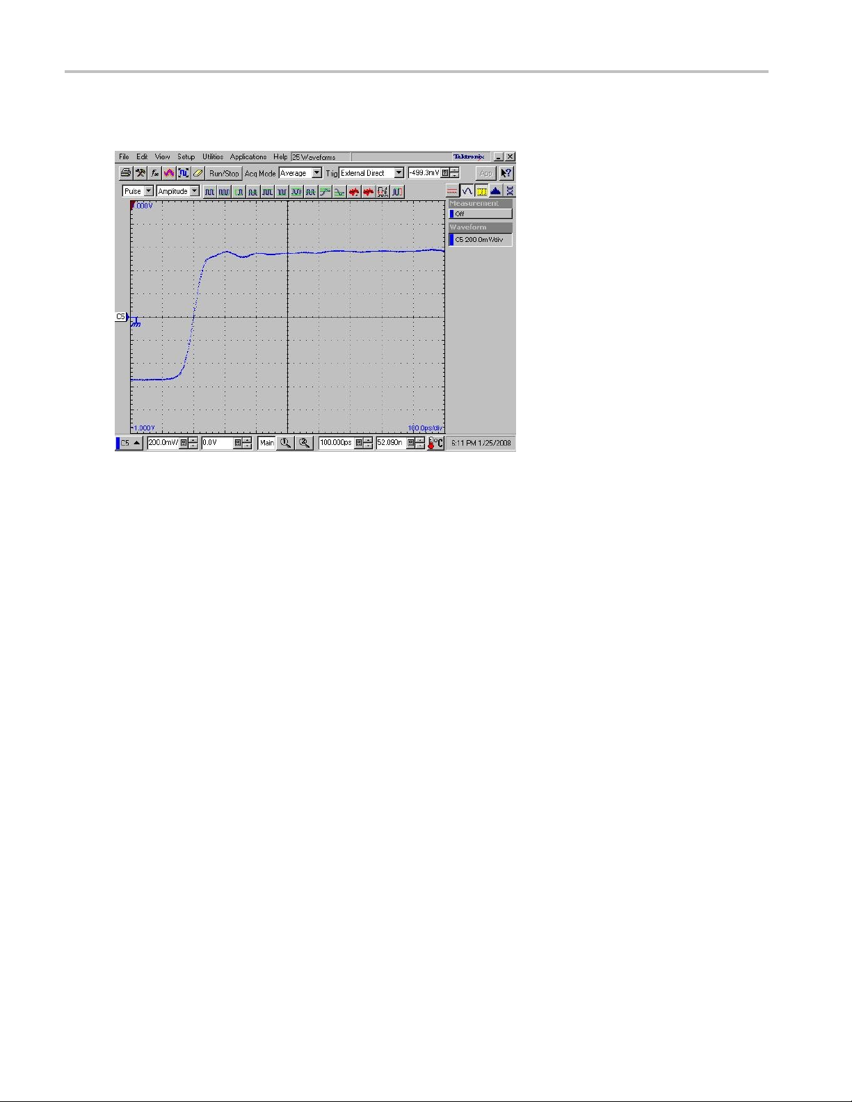
Specifications
The following figure shows the typical step response of the probe with the P75PDPM probing module. A 50 ps rise time
pulse source wa
s used for this measurement.
Figure 33: TriMode probe w ith the P75PDPM probing module
68 P7520A Probe Instruction M anual
Page 81

The following figure shows the typical differential impedance of the probe with the P75PDPM probing module.
Figure 34: P75PDPM differential impedance
Specifications
P7520A Probe Instruction M anual 69
Page 82

Service
Service
This section covers care, troubleshooting, and maintenance of your probe.
Host Instrument Firmware
Some instruments may require a firmware upgrade to support full functionality of the P7520A probe. Instruments with lower
versions of firmware may not display all probe controls and indicators on screen, and in some cases may require you to
power-cycle the instrument to restore normal instrument operation.
The following table lists the required versions of instrument firmware for some of the instruments that currently support
the P7520A probe.
Instrument Firmware Version
DPO/DSA70000D series oscilloscopes
DPO/DSA/MSO70000C series oscilloscopes with Windows
7, 64-bit OS
DPO/DSA/MSO70000B, C series oscilloscopes with
Windows XP, 32-bit OS
80A03 TekConnect Probe Adapter
RTPA2A TekConnect Probe Adapter
V 6.4.4 or higher
V 6.4.0 or higher
V 5.3.5 or higher
V 2.3 or higher
V 2.3 or higher
To check the firmware version on Windows-based instruments, from the menu bar, click Help/About TekScope. On
Linux-based instruments, press the Utilities button on the front panel. If you need to upgrade your instrument firmware, go to
www.tektronix.com/software to download the latest firmware.
Error Conditions
LED Indicators
If one of the Range or TriMode LEDs does not remain lit after you connect the probe, an internal probe diagnostic fault exists.
Disconnect and reconnect the probe to restart the power-on diagnostic sequence. If the symptoms continue, the probe is
defective, and must be returned to Tektronix for repair.
Atten (Range) Setting
If you cannot change the attenuation by pressing the Atten. button on the probe, the host instrument may be in Auto
Range mode. Change the range mode from Auto to Manual in the Probe Setup or Probe Controls screen. From the
oscilloscope menu bar, select Vertical/Probe Cal or Vertical/Probe Setup and then select Manual in the TriMode Probe
Range or Attenuation section.
Signal Display
If the probe is connected to an active signal source and you do not see the signal displayed on the oscilloscope:
Check the probe tip connection on your circuit. (See page 17, Connecting to a Circuit Board.)
Check the probe tip connection at the probe body. (See page 5, Connecting Accessories to the Probe Body.)
70 P7520A Probe Instruction M anual
Page 83

Service
Perform a functional check using the TriMode calibration board included with the probe. (See page 9, Functional Check.)
Check that the bullet contacts are present and intact in the probe body. (See page 75, Inspecting the Bullets and
Connectors.)
Input Mode/Probe Tip Selection
If you cannot select an Input Mode other than A – B, and you are using a TriMode tip that does not provide a circuit ground
connection (such as the P75PDPM handheld module), this is normal operation. The other input modes refer to circuit ground
and are only valid when a TriMode tip that provides a circuit ground connection is selected.
If you are using a TriMode tip that provides a circuit ground connection (such as the P75TLRST) and you cannot select
an Input Mode other than A – B, check the Probe Tip Selection screen on the oscilloscope. (See Figure 35 on page 71.)
An incorrect probe tip might be selected. To access the Probe Tip Selection screen, select Vertical/Probe Cal from the
menu bar, and then click Select in the Probe Tip section.
e 35: Probe Tip Selection screen
Figur
P7520A Probe Instruction M anual 71
Page 84

Service
Replaceable Parts
The following parts may need to be replaced due to normal wear and damage. When you replace these components, secure
the probe in a small vise or positioner to simplify the procedure.
Table 8: TriMode probes replaceable parts
Description Replacement part number
Probe body bullet contacts
P75TLRST and P75PST solder tip wires
TriMode Resistor (020-2936-xx) & TriMode
Extended Resistor (020-2944-xx) solder tip
resistors
P75PDPM Probing Module springs
P75PMT Probing Module tips (left and right)
P75TC Probing Module tip cable P75TC, qty. 1
013-0359-xx, kit of 4
020-2754-xx, W ire Replacement Kit, includes one bobbin each: 4 m il wire,
8 mil wire, and SAC305 solder
020-2937-xx Replacement Resistor Kit, includes 50 each:
100 Ω leaded resistors, 75 Ω surface mount resistors, nonconductive tubing
016-1998-xx, kit of 4 (large springs)
016-1999-xx, kit of 4 (small springs)
P75PMT, one pair
72 P7520A Probe Instruction M anual
Page 85

Table 9 : Required e quipment
Description Minimum r equirement Recommended example
Connector separator tool Custom tool
Ground spring tool Custom tool
Tweezers
General purpose
Magnifying glass or microscope Free standing to allow hands-free use
Probe positioner or bench vise Able to hold probe PPM203B or PPM100
1
Nine-digit part numbers (xxx-xxxx-xx) are Tektronix part numbers.
003-1897-xx
003-1900-xx
Service
1
P7520A Probe Instruction M anual 73
Page 86

Service
Bullet Contacts
The input sockets in the probe body
assembly are protected by replaceable bullet
contacts. (Replaceable bullets are included
in the accessory kit.)
The bullet contacts protect the input sockets
by absorbing the wear from repeated
connect/disconnect cycles of the accessory
tips.
A bullet tool is shipped with the probe and is
used to replace the bullet contacts from the
probe body assembly.
CAUTION. To prevent wear to the probe housing, use only the Bullet tool provided to remove and install the bullets from
the probe body assembly. To prevent damage to the probe, before you connect accessories to the probe body, always
check that the contacts are located in the probe body only.
Removing the Bullets
Follow these steps to remove the bullets by
using the removal tool:
1. Squeeze the tool plunger to extend the
angs.
holder t
2. Insert
3. Release the plunger to secure the holder
4. Gentl
5. Repeat for the other bullet.
NOTE. Discard the used bullets to prevent
acci
the tool into the probe body so
that the holder tangs surround one of the
bullets.
on the bullet.
tangs
y pull the tool outward to remove
the bullet.
dental reuse.
74 P7520A Probe Instruction M anual
Page 87
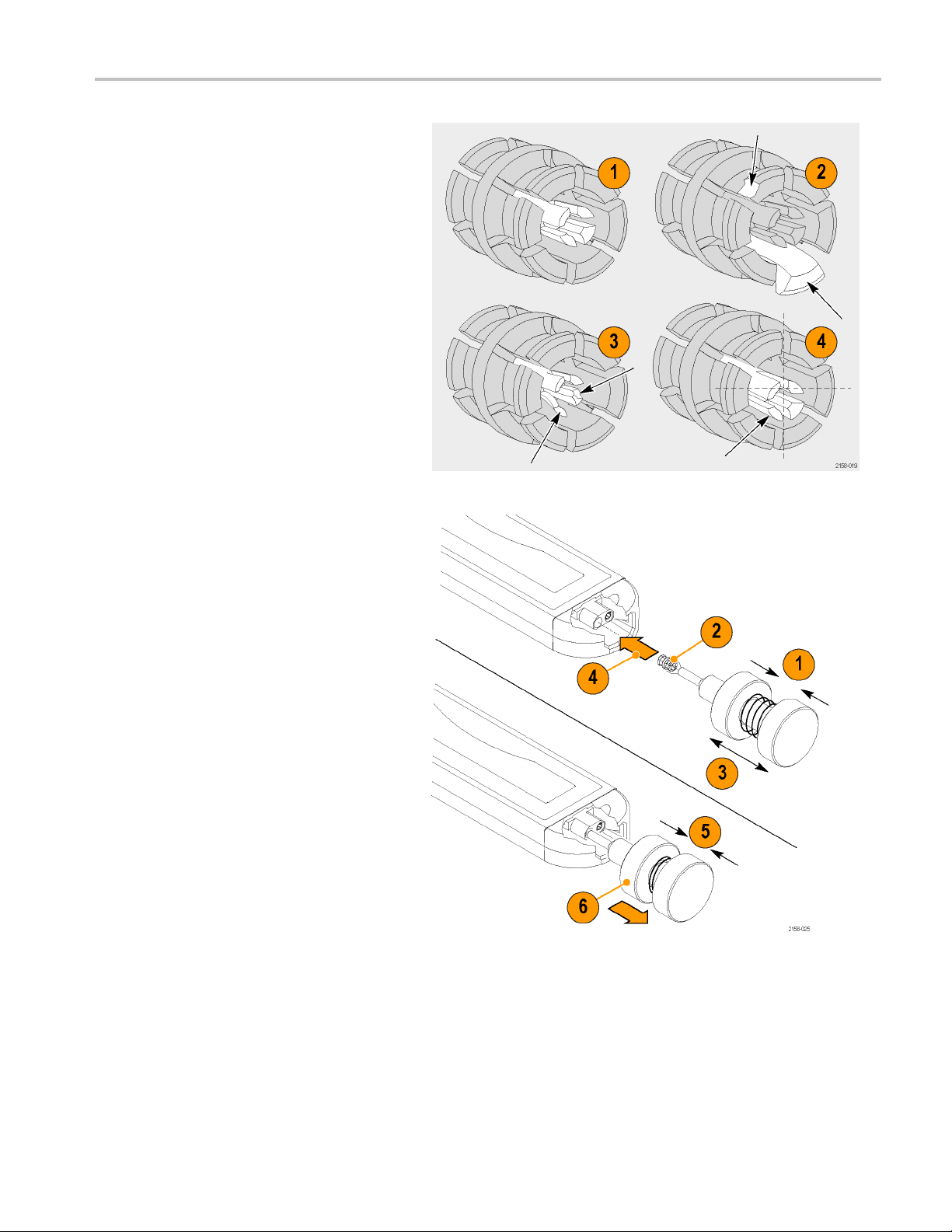
Inspecting the Bullets and
Connectors
Use a microscope to closely examine the
bullets and connectors. Use the illustrations
to determine if the contacts appear worn or
broken, and always replace them in pairs.
1. Good
2. Chipped or bent ground contacts (outer
conductor)
3. Chipped or bent signal contacts (inner
conductor)
4. Inner contacts misaligned to outer
conductor
Service
Installing the Bullets
1. Squeeze the tool plunger to extend the
holder tangs.
2. Insert a new bullet into the tool so that
the holder tangs surround the bullet.
3. Release the plunger to secure the holder
tangs on the bullet.
4. Insert the tool into the probe body and
seat the bullet in the recess.
5. Squeeze the tool plunger to release the
bullet.
6. Gently pull the tool out of the probe body.
7. Repeat for the other bullet.
8. Connect and remove a probe tip on the
probe body. Verify that the bullets are
retained in the probe body.
P7520A Probe Instruction M anual 75
Page 88
Service
Solder Tip Wires and Resistors
The solder vias on the circuit board at the end of the P75TLRST and P75PST Solder Tips are small (0.012 in.), and require
small wires to attach to your circuit. (Use the 4-mil and 8-mil wires included with the Wire Replacement kit to make the
connections.) Because of the small dimensions, the solder tips have a limited number of solder cycles that the vias can
withstand before the Solder Tips become unusable. If you e xpect to make frequent soldering changes, consider using the
optional TriMode Resistor solder tips. The resistors that extend off of these tips c an accept a higher number of solder
cycles and can be replaced when necessary.
NOTE. Axial-leaded tip resistors (included in the TriMode resistor replacement kit, Tektronix part number 020-2937-xx),
should not be used in place of w ires with the P75TLRST or P75PST probe tips unless the surface-mount, SMD0402 resistors
are also changed. The total probe tip resistance for the P7500 Series probes is designed to be 175 Ω.
CAUTION. To prevent damage to the circuit board or circuit board connections due to accidental movement of the probe
and soldered leads, we recommend that you secure the tip to the circuit board using the adhesive tip tape provided in your
accessory kit. You can also use other materials such as Kapton tape or hot glue.
To avoid damage to the tip or the circuit under test, avoid applying excessive heat from the soldering iron. Use a low wattage,
temperature-controlled soldering iron and appropriately sized soldering iron tip.
To prolong the life of your solder tips, consider the following points before you use the solder tips.
Consider the types of measurements that you plan to take. If you are going to take a few measurements at one location
and then move to another, you may be able to use longer wires. Longer wires may degrade your measurement slightly
(which may not matter), but the wires can then be cut or desoldered at your circuit and reused, rather than subjecting the
solder tip to a desolder/solder cycle.
Perhaps the optional P75PDPM Precision Differential Probing Module is a better choice for the test points that you do not
measure as often. The probing module can take both single-ended and differential measurements, and when used with a
probe positioner, can provide hands-free access to tight spaces. Depending on your measurement requirements and circuit
geometries, the probing module might be a preferable alternative.
At critical test points such as circuit outputs, you might need to keep the wires as short as possible. If possible, use the solder
tip dimensions shown in the Specifications section to lay out a matching footprint on your circuit b oard.
Use the following precautions when you solder the tips:
For best soldering results, use a microscope to examine the quality of the solder joints.
Use a low-wattage, temperature-controlled soldering iron and a small mass soldering iron tip. The soldering iron
temperature should be set as low as possible, while still providing a reliable solder joint.
Use SAC305 solder (included with the wire replacement kit) to attach the tip wires to the circuit under test.
When replacing tip wires or axial-lead res istors, solder wick can be used to remove the excess solder from the probe tip
circuit board via holes. Be careful not to overheat the via and damage the board.
The attachment wires should be bent symmetrically to vary the interconnect spacing. Use care when you solder a tip to a
circuit under test to avoid inadvertently desoldering either the attachment wires or the damping resistor.
For optimum performance and signal integrity, keep the lead length between the DUT (Device Under Test) and the tip as
short as possible, and the lead lengths the same length.
76 P7520A Probe Instruction M anual
Page 89

Replacing the TriMode Solder Tip
Resistors
The resistors that are presoldered to the
tips can break off during normal use. A kit
of replacement resistors is available. (See
page 30, Optional Accessories.) To replace
the resistors, do the following:
1. Carefullyapplyasolderingirontothevia
on the tip board and remove the resistor
lead. Work quickly with a low-heat
soldering iron.
If a small piece of wire is in the via, heat
the solder and use another piece of wire
to push the wire fragment from the via.
2. Add fresh solder to the via, if necessary.
3. Cut one lead of the replacement resistor
to approximately 0.6” (15 mm) for the
long tip, or 0.2” (5 mm) for the short tip.
Service
4. If you are replacing the resistor on the
extended resistor tip, slide a piece of
tubing included with the resistor kit over
the lead. This will insulate the resistor
lead.
5. Heat the solder in the via and insert the
resistor lead into the via until the:
insulating tube comes into c ontact with
the tip board, if you are replacing the
resistor on the extended resistor tip.
resistor body almost touches the tip
board, if you are replacing the resistor
on the (short) resistor tip.
6. Cut the excess lead on the bottom of the
board.
7. Cut the remaining resistor lead to 0.1”
(2.5 mm).
P7520A Probe Instruction M anual 77
Page 90

Service
P75PDPM Probing Module Springs
Equipment Required:
ground spring tool
tweezers
probe holder
magnifying glass or microscope
Large and small springs shown installed
Remove the Spring
1. Adjust the tip gap using the gap
measurement tab on the spring tool. Set
the tool between the tip circuit boards,
not the tips.
78 P7520A Probe Instruction M anual
Page 91

Service
2. Insert the grou
top of the spring.
nd spring tool under the
P7520A Probe Instruction M anual 79
Page 92

Service
3. Rock the tool away from the tips so that
the spring clears the seat edge.
4. Gently pull the tool away; the spring
should come aw
ay with the tool.
5. Put the sprin
or a safe place to avoid l osing the spring.
g in the accessory container
Install. Two spring sizes are available:
the small spring allows 0.030 – 0.090 in.
(0.76 – 2.28 mm) tip span, the large spring
allows 0.050 – 0.180 in. (1.27 – 4.57 mm)
tip span.
1. Check that the tip gap is .032 in. using
the gap measurement tab on the spring
tool. Adjust if necessary.
80 P7520A Probe Instruction M anual
Page 93

Service
2. Using tweezers
, install the spring on the
tool. The tool has a large and small side,
one for each size spring. Make sure the
gap in the spri
ng is on the top of the tool
as shown.
3. Set the bottom of the spring in the front
seats (those closest to the tip ends).
Maintain a slight pressure on the spring
to keep it in the front seats.
P7520A Probe Instruction M anual 81
Page 94

Service
4. Set the top of the spring in the rear seats
by lifting the tool to clear the edge of the
rear seat with
the top of the spring.
5. Gently retract the tool from the spring.
Verify that the spring is seated as shown.
82 P7520A Probe Instruction M anual
Page 95

P75TC Probing Module Tip Cable
Equipment Required: connector separator
tool
1. Disconnect the Cable Tip by the inserting
the tool between the connectors.
The tapered edges of the tool gently
separate the cable c onnector from the
tip connector.
2. Repeat for the other cable and then
pull both cables away from the tip
connectors.
Service
P7520A Probe Instruction M anual 83
Page 96
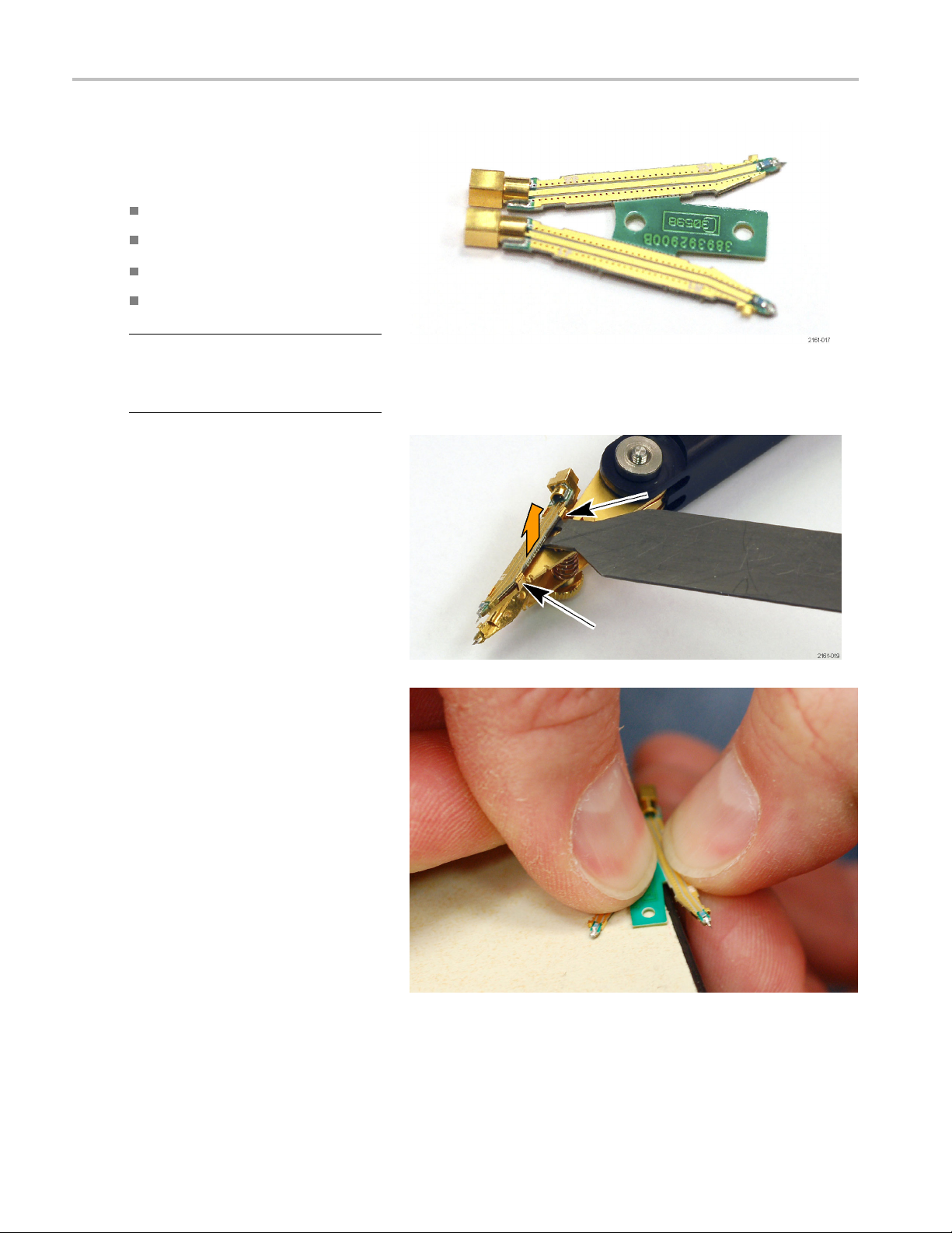
Service
P75PMT Probing Module Tips (Left
and Right)
Equipment Required:
connector separator tool
tweezers
probe holder
magnifying glass or microscope
(preferred)
NOTE. The probing module tips are
electrically matched pairs and should be
replaced together. Failure to do so may
degrade the performance of your probe.
Remove.
1. Disconnect the Cable Tips.
2. Remove the spring.
3. Adjust the tip gap to maximum width.
4. Use the connector separator tool or a
small screwdriver to pry the board up
from the bottom. The bottom tabs are
designed to flex; the top tabs are not.
5. Repeat for the other tip.
Install.
6. Separate the new tip board pair by
snapping the board against a sharp
edge.
84 P7520A Probe Instruction M anual
Page 97
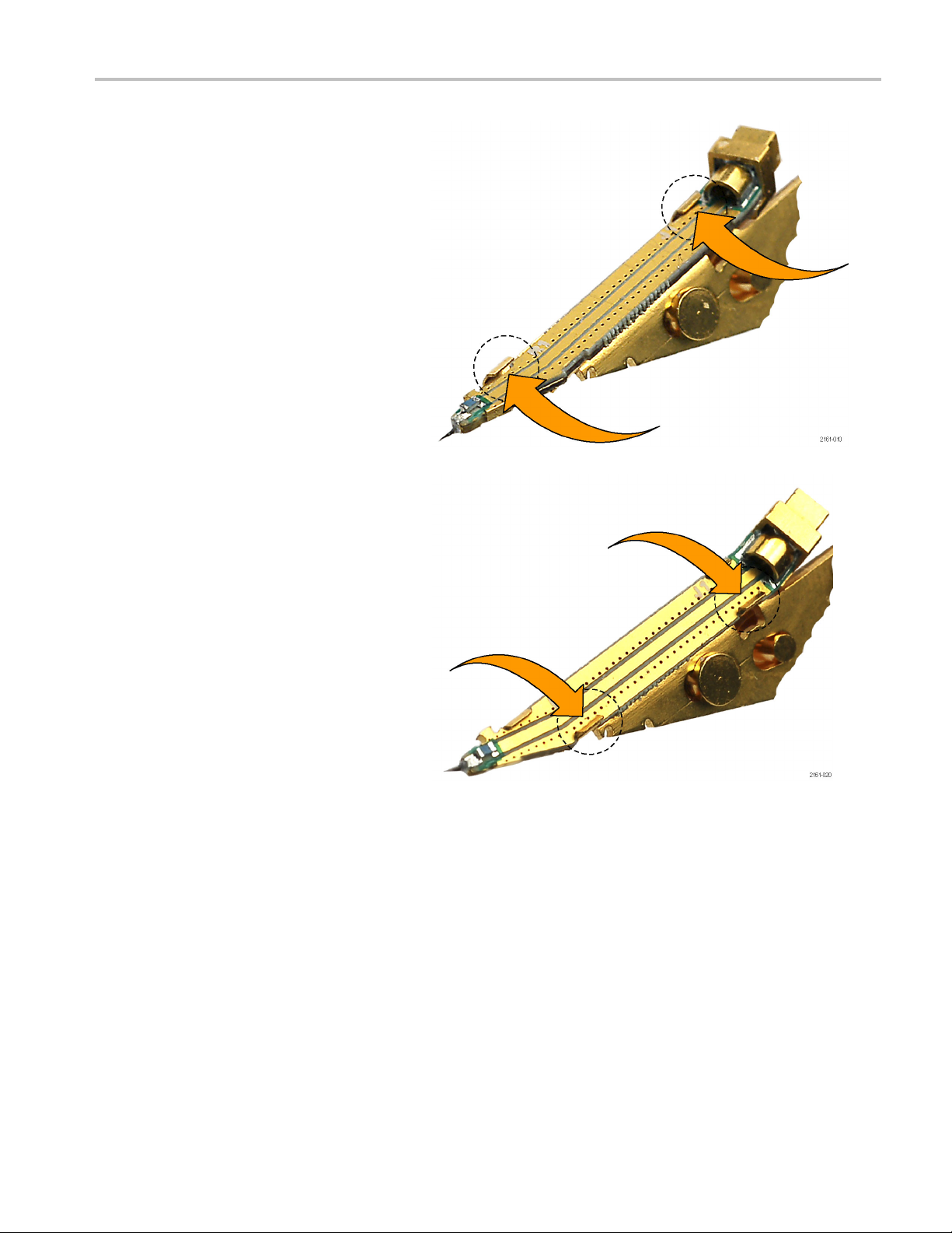
7. Select the correct board (left or right),
and seat the board in the top tabs. The
board is notch
ed to align it to the tip body.
Service
8. Press the
bottom of the board to snap it
past the bottom tabs.
9. Repeat the previous two steps for the
other tip.
10. Attach the spring.
11. Reattach the cable pair.
P7520A Probe Instruction M anual 85
Page 98

Service
Handling the Probe
This probe is a precision high-frequency device; exercise care when you use and store the probe. The probe and cable
are susceptible to damage caused by careless use. Always handle the probe at the control box and probe body to avoid
undue physical strain to the probe cable, such as kinking, excessive bending, or pulling. Visible dents in the cable will
increase signal aberrations.
CAUTION. To prevent damage to the probe, always use an antistatic wrist strap connected to a static-controlled workstation
when you handle the probe. The probe input contains electronic components that can be damaged by contact with high
voltages, including static discharge.
Observe the following precautions when using the probe. Do not do any of the following:
Drop the probe or subject it to physical shock
Subject the probe to adverse weather conditions
Kink or fold the probe cable tighter than a 2 inch radius
Solder the tips with excessive heat or duration
Injure yourself with the sharp tips
86 P7520A Probe Instruction M anual
Page 99

Cleaning the Probe
Service
CAUTION. To p r
the probe during exterior cleaning.
Do not use chemical cleaning agents; they may damage the probe. Avoid using chemicals that contain benzine, benzene,
toluene, xylene, ace
Clean the exterior s
dampened with a 75% isopropyl alcohol solution and rinse with deionized water. A swab is useful to clean narrow spaces on
the probe; use only enough solution to dampen the swab or cloth. Do not use abrasive compounds on any part of the probe.
event damage to the probe, do not expose it to sprays, liquids, or solvents. Avoid getting moisture inside
tone, or similar solvents.
urfaces of the probe with a dry, lint-free cloth or a soft-bristle brush. If dirt remains, use a s oft cloth or swab
P7520A Probe Instruction M anual 87
Page 100

Service
Returning the Probe for Servicing
If your probe requires servicing, you must return it to Tektronix. If the original packaging is unfit for use or not available, use
the following packaging guidelines:
Preparation for Shipment
1. Use a corruga
carton having inside dimensions at
least one inch greater than the probe
dimensions
carton test strength of at least 200
pounds.
2. Put the probe into an antistatic bag or
wrap it to p
3. Place the p
it with light packing material.
4. Seal the carton with shipping tape.
5. Refer to Contacting Tektronix at the
beginning of this manual for the shipping
address.
ted cardboard s hipping
. The box should have a
rotect it from dampness.
robe into the box and stabilize
88 P7520A Probe Instruction M anual
 Loading...