

Page 1

Instruction Manual
P7380SMA
8 GHz Differential Probe
071-1392-01
Warning
The servicing instructions are for use by qualified
personnel only. To avoid personal injury, do not
perform any servicing unless you are qualified to
do so. Refer to all safety summaries prior to
performing service.
www.tektronix.com
Page 2

Copyright © Tektronix, Inc. All rights reserved.
Tektronix products are covered by U.S. and foreign patents, issued and
pending. Information in this publication supercedes that in all previously
published material. Specifications and price change privileges reserved.
Tektronix, Inc., P.O. Box 500, Beaverton, OR 97077
TEKTRONIX, TEK, and TekConnect are registered trademarks of
Tektronix, Inc.
Page 3

WARRANTY
Tektronix warrants that the products that it manufactures and sells will be free from defects
in materials and workmanship for a period of one (1) year from the date of shipment. If a
product proves defective during this warranty period, Tektronix, at its option, either will
repair the defective product without charge for parts and labor, or will provide a
replacement in exchange for the defective product.
In order to obtain service under this warranty, Customer must notify Tektronix of the
defect before the expiration of the warranty period and make suitable arrangements for the
performance of service. Customer shall be responsible for packaging and shipping the
defective product to the service center designated by Tektronix, with shipping charges
prepaid. Tektronix shall pay for the return of the product to Customer if the shipment is to
a location within the country in which the Tektronix service center is located. Customer
shall be responsible for paying all shipping charges, duties, taxes, and any other charges for
products returned to any other locations.
This warranty shall not apply to any defect, failure or damage caused by improper use or
improper or inadequate maintenance and care. Tektronix shall not be obligated to furnish
service under this warranty a) to repair damage resulting from attempts by personnel other
than Tektronix representatives to install, repair or service the product; b) to repair damage
resulting from improper use or connection to incompatible equipment; c) to repair any
damage or malfunction caused by the use of non-Tektronix supplies; or d) to service a
product that has been modified or integrated with other products when the effect of such
modification or integration increases the time or difficulty of servicing the product.
THIS WARRANTY IS GIVEN BY TEKTRONIX IN LIEU OF ANY OTHER
WARRANTIES, EXPRESS OR IMPLIED. TEKTRONIX AND ITS VENDORS
DISCLAIM ANY IMPLIED WARRANTIES OF MERCHANTABILITY OR
FITNESS FOR A PARTICULAR PURPOSE. TEKTRONIX’ RESPONSIBILITY
TO REPAIR OR REPLACE DEFECTIVE PRODUCTS IS THE SOLE AND
EXCLUSIVE REMEDY PROVIDED TO THE CUSTOMER FOR BREACH OF
THIS WARRANTY. TEKTRONIX AND ITS VENDORS WILL NOT BE LIABLE
FOR ANY INDIRECT, SPECIAL, INCIDENTAL, OR CONSEQUENTIAL
DAMAGES IRRESPECTIVE OF WHETHER TEKTRONIX OR THE VENDOR
HAS ADVANCE NOTICE OF THE POSSIBILITY OF SUCH DAMAGES.
Page 4

Page 5

Table of Contents
Preface vii............................................
Contacting Tektronix viii.................................
General Safety Summary ix..............................
Service Safety Summary xi..............................
Getting Started 1.....................................
Probe Controls and Connections 2........................
Standard Accessorie s 6.................................
Optional Accessories 8.................................
Options 10............................................
TekConnect Interface 11.................................
Probe Inputs 12........................................
SMA Connectors 12.................................
DC Termination Voltage Control Jacks 13................
Probe Input Limitations 13............................
Probe Outputs 14......................................
Termination Voltage Monitor Jacks 14...................
Auxiliary Output SMA Connector 14....................
Functional Check 15....................................
Power-on Self Test 16................................
Signal and Termination Voltage Monitor Check 17.........
Aux Output Check 20................................
DC Termination Voltage Zero Check 22.................
Probe Calibration 24....................................
Using the Probe 26.....................................
Auto Mode 26......................................
External Mode 27...................................
Internal Mode 28....................................
Auxiliary Output 29.................................
Using the Probe With a Sampling Oscilloscope 30.........
P6150 Probe Tips 32.................................
Operating Basics 33...................................
Differential Measurements for Serial Data Compliance Testing 33
Differential Signalling 33.............................
Pseudo-Differential Measurements 34...................
Differential Probe Measurements 35....................
Common-Mode Rejection Ratio 36.....................
P7380SMA 8 GHz Differential Probe Instruction Manual
i
Page 6

Table of Contents
Probe Block Diagram (Simplified) 37......................
Matched-Delay Cables 37.............................
Input Termination Network 38.........................
Internal Probe Amplifier 40...........................
Termination Voltage Control 44...........................
Auto Mode 45......................................
Int Mode 45........................................
Ext Mode 45.......................................
Overdrive Error 4 7.....................................
Differential and Single-Ended Signal Measurement 48.........
Differential Measurement Topology 48..................
Differential Dynamic Range 49........................
Single-Ended Measurement Topology 50.................
Single-Ended Measurement Procedure 54................
Single-Ended Dynamic Range 55.......................
Extending the Input Connections 56.......................
Checking Cable Skew 57................................
Adjusting Cable Skew 58................................
Deskewing Probes 60...................................
Reference 63.........................................
Serial Bus Standards 63.................................
InfiniBand 64.........................................
ii
P7380SMA 8 GHz Differential Probe Instruction Manual
Page 7

Table of Contents
Appendix A: Specifications 65...........................
Warranted Characteristics 65.............................
Typical Characteristics 66...............................
Nominal Characteristics 71..............................
Mechanical Characteristics 71............................
Appendix B: Performance Verification 73.................
Equipment Required 73.................................
Special Adapters Required 75............................
TekConnect-to-SMA Adapter 75.......................
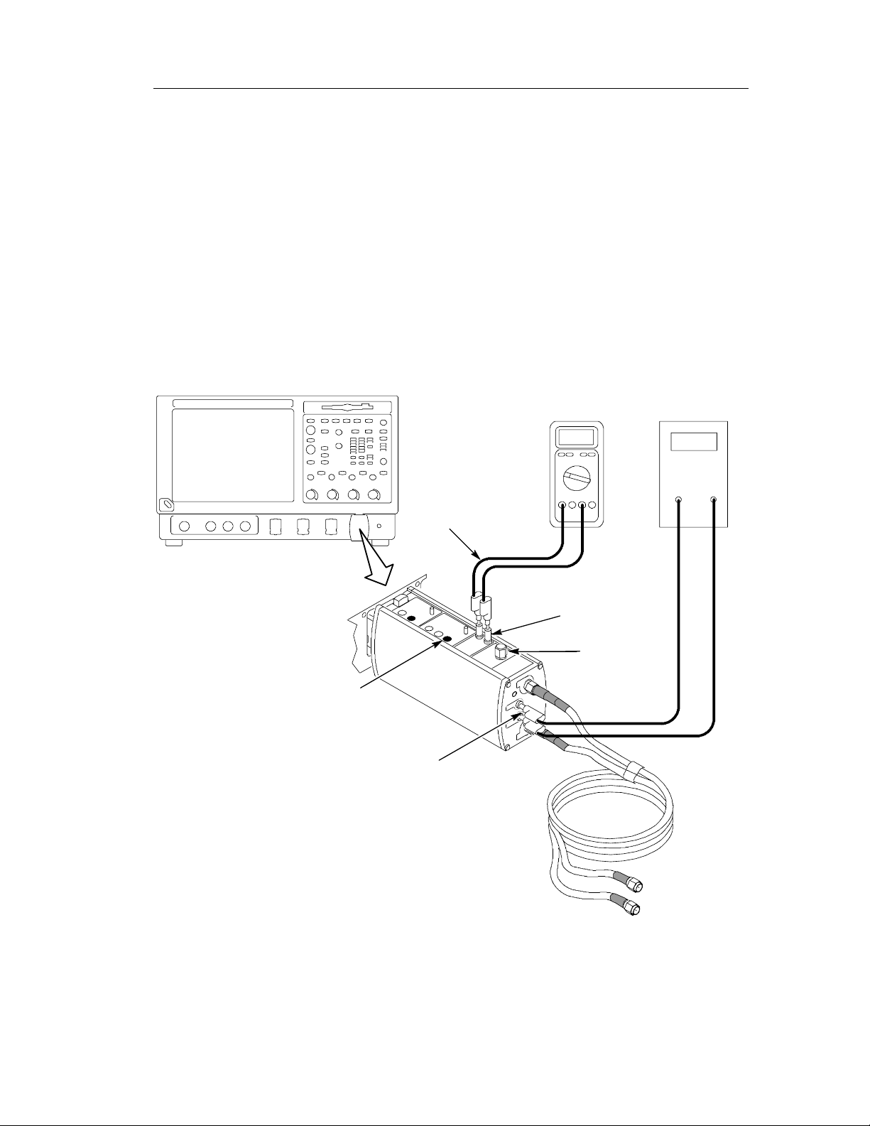
Equipment Setup 76....................................
Input Resistance 77.....................................
Termination Voltage Accuracy 78.........................
Ext Mode 78.......................................
Int Mode 79........................................
Auto Mode 80......................................
Output Offset Zero 82...................................
DC Gain Accuracy 83...................................
Gain Check at 2.5X Attenuation 83.....................
Gain Check at 12.5X Attenuation 85....................
Rise Time 85..........................................
Rise Time Check at 12.5X Attenuation 85................
Rise Time Check at 2.5X Attenuation 89.................
Appendix C: User Service 91............................
Probe/Adapter/Oscilloscope Compatibility 91................
Check Compatibility 91..............................
Error Conditions 92....................................
Inspection and Cleaning 93..............................
Replacement Parts 93...................................
Preparation for Shipment 94..............................
P7380SMA 8 GHz Differential Probe Instruction Manual
iii
Page 8

Table of Contents
List of Tables
Table 1: P7380SMA features 2..........................
Table 2: P7380SMA standard accessories 6................
Table 3: Optional accessories 8..........................
Table 4: Equipment required for functional checks 15.........
Table 5: Common-mode voltage and current table 39.........
Table 6: Differential to single-ended conversion table 55......
Table 7: Serial bus standards with
dynamic range requirements 63........................
Table 8: Warranted electrical characteristics 65..............
Table 9: Typical electrical characteristics 66................
Table 10: Nominal electrical characteristics 71..............
Table 11: Typical mechanical characteristics 71..............
Table 12: Equipment required for performance verification 73..
Table 13: P7380SMA probe compatibiity issues 91...........
Table 14: LED error conditions 92........................
iv
P7380SMA 8 GHz Differential Probe Instruction Manual
Page 9

List of Figures
Figure 1: P7380SMA differential probe 1..................
Figure 2: Connecting and disconnecting the probe 11..........
Figure 3: Probe signal input connections 12.................
Figure 4: Signal check setup 17...........................
Figure 5: Aux output check test setup 20....................
Figure 6: DC termination voltage check setup 22.............
Figure 7: Probe calibration setup 25........................
Figure 8: Using Auto Termination Voltage Control Mode 26....
Figure 9: Using External Termination Voltage Control Mode 27.
Figure 10: Using Internal Termination Voltage Control Mode 28.
Figure 11: Viewing the Aux Out signal on a spectrum analyzer 29
Figure 12: Using the probe with an 80A03 Interface and an 80A05
Module to view eye diagrams on a TDS8000 Series sampling
oscilloscope 31.....................................
Figure 13: P6150 probe tips 32............................
Figure 14: Simplified model of a differential amplifier 36......
Figure 15: Input termination network 37....................
Figure 16: Probe maximum input limits 42..................
Figure 17: Differential and Common-Mode operating ranges 43.
Figure 18: Termination voltage network drive 44.............
Figure 19: Overdrive Error indicator 47.....................
Figure 20: Differential measurement topology 48.............
Figure 21: 50 ohm termination on (--) input 51...............
Figure 22: Shorting termination on (--) input 52..............
Figure 23: Open (--) input 53.............................
Figure 24: Checking skew between inputs 57................
Figure 25: Using the phase adjuster 59.....................
Figure 26: Deskewing two P7380SMA probes 61.............
Figure 27: InfiniBand signals 64..........................
Figure 28: Typical CMRR plot 68.........................
Figure 29: Typical differential input return loss 69............
Figure 30: Typical differential-mode bandwidth 69............
Figure 31: Typical eye pattern from an InfiniBand signal 70....
Figure 32: Typical differential step response 70..............
Figure 33: Probe dimensions 72...........................
Figure 34: TekConnect-to-SMA Adapter 75.................
Figure 35: Preliminary test setup 76........................
Table of Contents
P7380SMA 8 GHz Differential Probe Instruction Manual
v
Page 10

Table of Contents
Figure 36: Checking differential mode input resistance 77......
Figure 37: Termination Voltage Accuracy, Ext mode setup 78...
Figure 38: Termination Voltage Accuracy, Auto mode setup 80..
Figure 39: Setup for the output offset zero test 82.............
Figure 40: DC Gain Accura cy setup 83.....................
Figure 41: Reverse the power supply polarity
on the probe inputs 84................................
Figure 42: Test system rise time setup 86...................
Figure 43: Setting the TDR parameters 87...................
Figure 44: Test system rise time setup with probe 88..........
vi
P7380SMA 8 GHz Differential Probe Instruction Manual
Page 11

Preface
This is the Instruction Manual for the P7380SMA differential probe.
This manual provides operating information, specifications, and
performance verification procedures for the probe.
P7380SMA 8 GHz Differential Probe Instruction Manual
vii
Page 12

Preface
Contacting Tektronix
Phone 1-800-833-9200*
Address Tektronix, Inc.
Department or name (if known)
14200 SW Karl Braun Drive
P.O. Box 500
Beaverton, OR 97077
USA
Web site www.tektronix.com
Sales
1-800-833-9200, select option 1*
support
Service
1-800-833-9200, select option 2*
support
Technical
www.tektronix.com/support
support
1-800-833-9200, select option 3*
6:00 a.m. -- 5:00 p.m. Pacific Standard Time
* This phone number is toll free in North America. After office hours, please
leave a voice mail message.
Outside North America, contact a Tektronix sales office or distributor; see
the Tektronix web site for a list of offices.
viii
P7380SMA 8 GHz Differential Probe Instruction Manual
Page 13

General Safety Summary
Review the following safety precautions to avoid injury and prevent
damage to this product or any products connected to it. To avoid
potential hazards, use this product only as specified.
To Avoid Fire or Personal Injury
Connect and Disconnect Properly. Connect the probe output to the
measurement instrument before connecting the probe to the circuit
under test. Disconnect the probe input from the circuit under test
before disconnecting the probe from the measurement instrument.
Observe All Terminal Ratings. To avoid fire or shock hazard, observe all
ratings and markings on the product. Consult the product manual for
further ratings information before making connections to the product.
The common terminal is at ground potential. Do not connect the
common terminal to elevated voltages.
Do Not Operate Without Covers. Do not operate this product with
covers or panels removed.
Do Not Operate With Suspected Failures. If you suspect there is damage
to this product, have it inspected by qualified service personnel.
Do Not Operate in Wet/Damp Conditions.
Do Not Operate in an Explosive Atmosphere.
Keep Product Surfaces Clean and Dry.
P7380SMA 8 GHz Differential Probe Instruction Manual
ix
Page 14
General Safety Summary
Safety Terms and Symbols
Terms in This Manual. These terms may appear in this manual:
WARNING. Warning statements identify conditions or practices that
could result in injury or loss of life.
CAUTION. Caution statements identify conditions or practices that
could result in damage to this product or other property.
Terms on the Product. These terms may appear on the product:
DANGER indicates an injury hazard immediately accessible as you
read the marking.
WARNING indicates an injury hazard not immediately accessible as
you read the marking.
CAUTION indicates a hazard to property including the product.
Symbols on the Product. These symbols may appear on the product:
CAUTION
Refer to Manual
x
P7380SMA 8 GHz Differential Probe Instruction Manual
Page 15

Service Safety Sum mary
Only qualified personnel should perform service procedures. Read
this Service Safety Summary and the General Safety Summary before
performing any service procedures.
Do Not Service Alone. Do not perform internal service or adjustments
of this product unless another person capable of rendering first aid
and resuscitation is present.
P7380SMA 8 GHz Differential Probe Instruction Manual
xi
Page 16

Service Safety Summary
xii
P7380SMA 8 GHz Differential Probe Instruction Manual
Page 17
Getting Started
The P7380SMA is an 8 GHz, active differential probe designed for
Serial Data Analysis (SDA) compliance testing and other applications that use differential serial busses in a 50 Ω signaling environ-
ment. The SMA input connectors each terminate with an internal
50 Ω resistor. The internal 50 Ω resistors are not dire ctly grounded,
but are driven by a buffer amplifier to a common-mode DC
termination voltage. The termination voltage range allows the
termination voltage to be set to any value within the specified
common mode voltage range of the input signal.
The DC termination voltage can be supplied either externally or
internally, including an automatic mode that sets the value of the
termination voltage to match the input signal DC common-mode
voltage. The P7380SMA probe has two selectable attenuator settings
that provide a tradeoff between dynamic range and noise. The
P7380SMA probe has been optimized for a clean pulse response for
accurate SDA compliance testing.
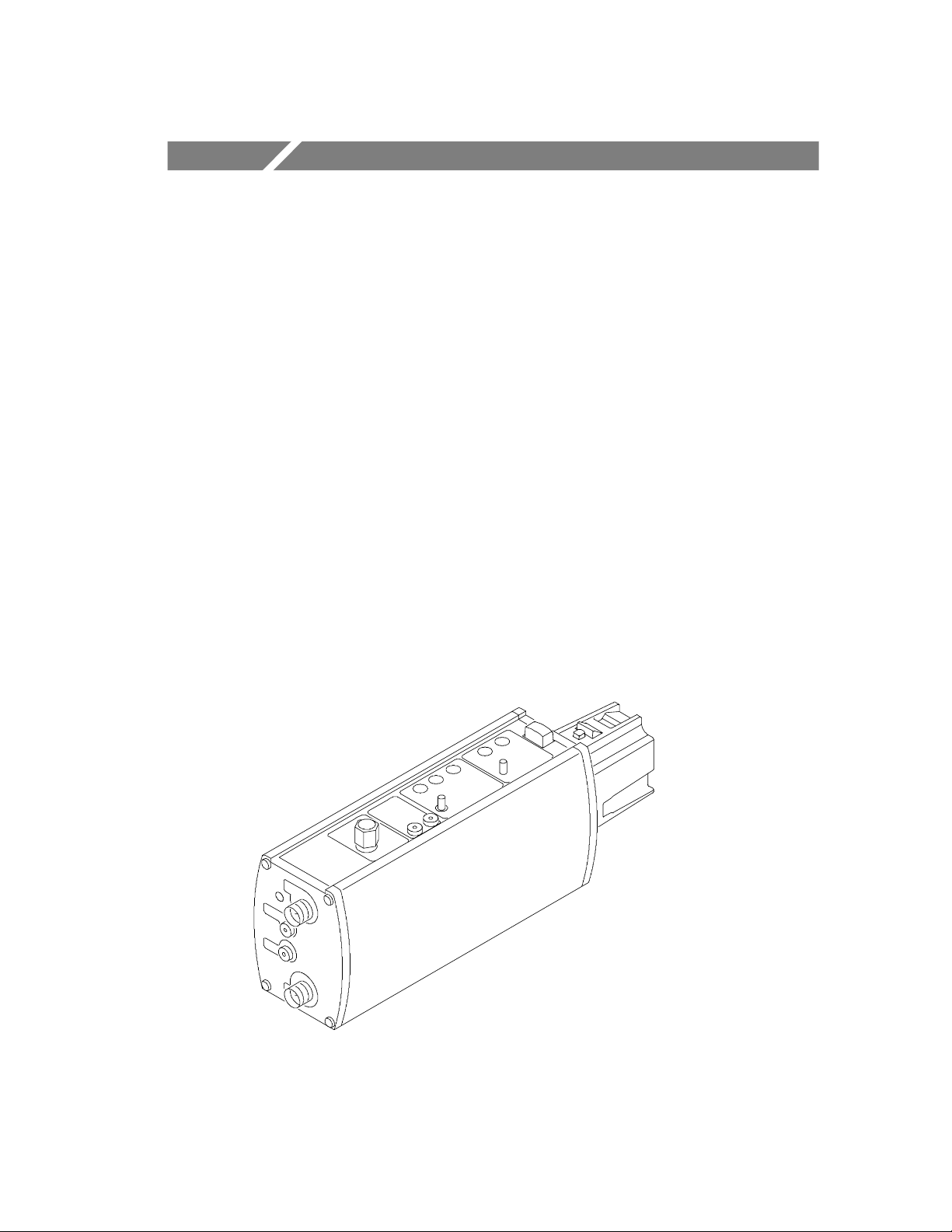
Figure 1: P7380SMA differential probe
P7380SMA 8 GHz Differential Probe Instruction Manual
1
Page 18
Getting Started
The probe incorporates the high-performance TekConnect interfa ce
to communicate with the host instrument. In addition to the acquired
signal that is routed through the TekConnect interface, the probe also
provides a full-bandwidth, inverted-phase auxiliary output. The
auxiliary output can be used for additional signal analysis by
connecting it to a spectrum analyzer, network analyzer, or clock
recovery unit.
The probe is shipped with 50 Ω termination caps connected to the
three SMA input and output connectors. When you are not using the
probe, leave the termination caps connected to protect the circuitry
from damage.
Always leave the Auxiliary output connector terminated when not in
use, to provide the best signal fidelity for the main probe output.
Probe Controls and Connections
Table 1 briefly outlines the controls and c onnections of the
P7380SMA differential probe. Additional information can be found
later in Getting Started and the following Operating Basics sections.
Table 1: P7380SMA features
Control/Connection Description
TekConnect interface. The TekConnect interface provides a
communication path between the probe and the oscilloscope.
Contact pins provide power, signal, offset, and probe characteristic data transfer.
The probe snaps into the oscilloscope when fully engaged. To
remove, grasp the compensation box, press the latch button, and
pull the probe out.
For more information, see page 11.
2
P7380SMA 8 GHz Differential Probe Instruction Manual
Page 19
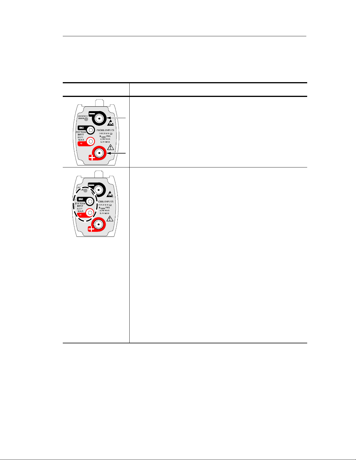
Table 1: P7380SMA features (Cont.)
Control/Connection Description
Input signal connections. The SMA terminals provide shielded,
low-noise connections to your circuit. Differential or single-ended
signals are buffered by the internal probe amplifier and are sent
through the TekConnect interface to the oscilloscope.
See Probe Inputs on page 12 for more information.
External DC termination control voltage connections. The red
and black 0.080 in jacks on the end of the probe provide a means
for controlling the DC termination voltage with an external DC
power supply.
Getting Started
You should use the Banana-to-0.080 in plug adapter cables
included with the probe when connecting external control voltages
to these terminals.
The Overdrive Error LED glows continually red when the
termination voltage driver current exceeds its linear range.
In general, this will occur when the termination voltage differs from
the common-mode voltage by about 2.0 volts for zero-ohm source
impedances and about 4.0 volts for 50 ohm source impedances.
The Overdrive Error LED flashes when the termination voltage in
Auto Mode or EXT Mode exceeds the specified ±2.5 volt range by
about 10%.
The Overdrive Error LED clears when the range violation signal is
removed.
For more information, see pages 13 and 47.
P7380SMA 8 GHz Differential Probe Instruction Manual
3
Page 20
Getting Started
Table 1: P7380SMA features (Cont.)
Control/Connection Description
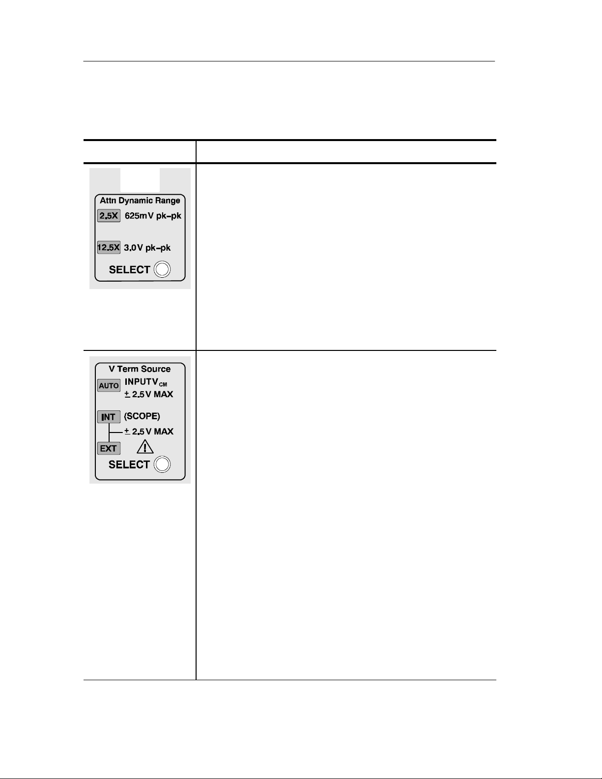
Attenuation/Dynamic Range Select and indicators. The Atten
Dynamic Range Select button allows you to select between 2.5X
and 12.5X probe attenuation settings. Note that the maximum
linear dynamic range for each attenuator setting is specified as a
differential peak-to-peak value.
The two indicator LEDs light briefly when the probe is powered
on, and then the 12.5X LED lights to indicate the 12.5X
attenuation is selected.
If both LEDs flash, an internal probe diagnostic fault exists.
Disconnect and reconnect the probe to restart the power-on
diagnostic sequence. If the LEDs continue to flash, the probe is
defective, and must be returned to Tektronix for repair.
1
Termination Voltage Control Mode Select and indicators.
The V Term Source Select button allows you to select between
three termination voltage control modes—Auto, Internal, and
External. The three indicator LEDs light briefly when the probe is
powered on, and then the Auto LED lights.
1
The probe initially sets to Auto mode; press the SELECT button to
choose another mode. The Auto Mode LED also flashes when the
probe signal inputs are AC-coupled or open-circuit. When this
happens, the termination voltage is set to 0.0 V.
In Auto mode, the input signal DC common mode voltage is
measured and the DC termination voltage is automatically set to
equal that voltage. This is the default mode setting when the
probe is powered on.
In Internal mode, the DC termination voltage is set with user
interface controls that are available on TekConnect-interface
oscilloscopes that support this mode. If your oscilloscope does not
support this mode, the termination voltage defaults to 0 volts.
In External mode, the DC termination voltage is controlled
indirectly with an external DC power supply connected to the
0.080 in pin jacks on the probe face plate. If these control voltage
inputs are left open, the termination voltage defaults to 0 volts.
4
P7380SMA 8 GHz Differential Probe Instruction Manual
Page 21
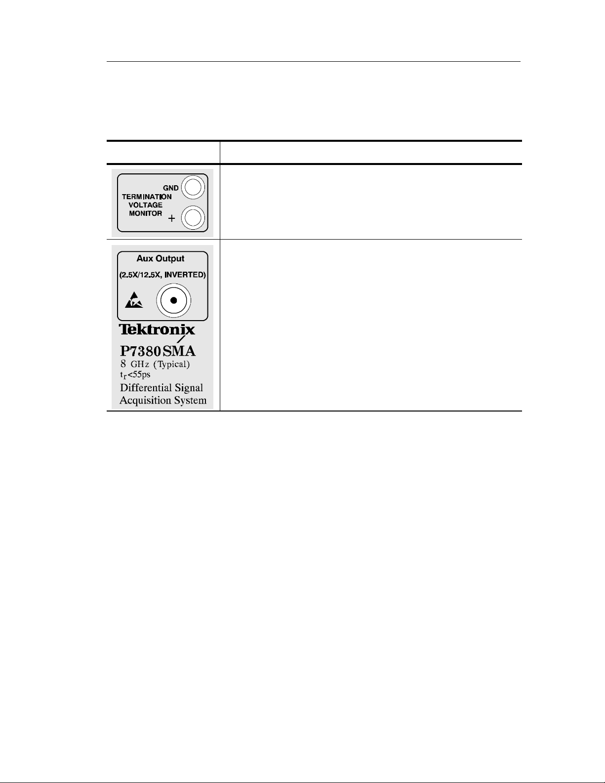
Table 1: P7380SMA features (Cont.)
Control/Connection Description
Termination Voltage Monitor jacks. These red and black jacks
provide a means for connecting a DMM to the probe to monitor
the DC termination voltage. For example, this can be used in Auto
mode to indirectly measure the DC common-mode input voltage.
Auxiliary Output connector. This SMA connector provides a
full-bandwidth, attenuated, inverted sample of the input signal.
Use this auxiliary signal to trigger your TDS/CSA 8000 series
sampling oscilloscope, or as an input to a spectrum analyzer or
network analyzer to measure the frequency domain response of
the input signal.
Getting Started
When you are not using this connector, leave the termination cap
connected to protect the SMA output connector from damage and
to ensure maximum signal fidelity of the main probe output signal
to the oscilloscope.
1
If the Attenuation and Termination Source LEDs do not light as described,
the host oscilloscope may have stored different attenuation and termination
source settings from a previous session. Use the SELECT buttons on the
probe to change the settings if necessary.
P7380SMA 8 GHz Differential Probe Instruction Manual
5
Page 22
Getting Started
Standard Accessories
Table 2 shows the standard accessories included with the P7380SMA
differential probe. To order replacements, use the Tektronix part
number listed with each accessory.
Table 2: P7380SMA standard accessories
Accessory Description
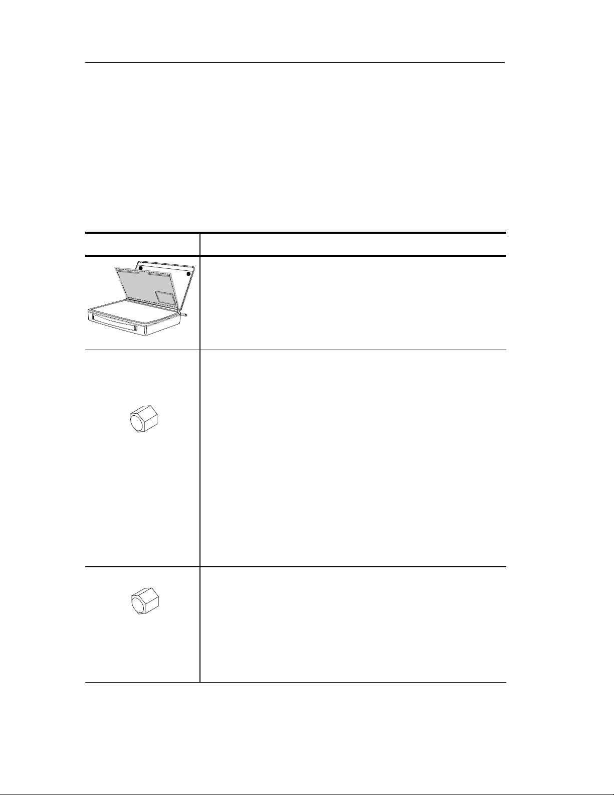
Carrying case with inserts. The soft-sided nyloncarrying casehas
several compartments to hold the probe, accessories, and related
documentation. Use the case to store or transport the probe.
Tektronix part number 016-1952-XX
Male SMA 50 Ω termination (3 ea). The probe is shipped with
these terminations connected to the probe SMA inputs and the
Auxiliary Output connector. Protect the probe circuitry by
connecting the terminations to these connectors when the probe
is not in use.
When making single-ended measurements in a 50 Ω
environment, one of these terminations may be used on the
unused input.
Only remove the 50 Ω termination from the Auxiliary Output
connector when you connect the Auxiliary Output to another
measurement instrument, such as a network analyzer. Otherwise,
leave the termination connected to the probe.
Tektronix part number: 015-1022-XX (package of 1)
Male SMA short-circuit. Use this adapter when performing a
functional check on the probe.
The SMA short-circuit may also be used to terminate an unused
input in one possible single-ended measurement topology.
See page 52 for more information.
Tektronix part number: 015-1020-XX
6
P7380SMA 8 GHz Differential Probe Instruction Manual
Page 23
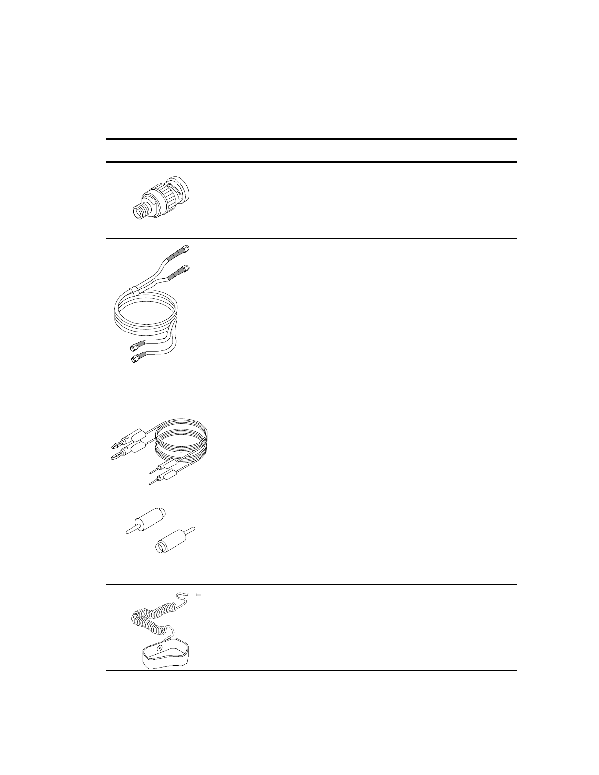
Table 2: P7380SMA standard accessories (Cont.)
Accessory Description
SMA Female-to-BNC Male adapter. Use the adapter to connect
the probe SMA inputs to BNC connections, such as the BNC
calibration output connector on your oscilloscope.
Tektronix part number: 015-0572-XX
Dual SMA cables. These 38 in cables are bound together and
have factory-calibrated integral phase adjusters to limit
cable-to-cable skew to less than 1 ps. (See page 8 for external,
user-adjustable phase adjusters.) The cables are color-coded at
each end for easy identification, and provide matched signal paths
from your circuit to the probe to ensure accurate differential signal
measurements. The P7380SMA differential probe includes built-in
cable loss compensation when used with the cable assembly.
Getting Started
Note: To make DUT connections easier, connect the phaseadjuster ends of the cables to the probe inputs.
Tektronix part number: 174-4944-XX
0.080 in Pin-to-Banana plug adapter cables. Use these cables
in external mode to control the DC termination voltage, using an
external power supply to set the value.
Tektronix part number: 012-1674-XX (red), 012-1675-XX (black)
0.040 in-to-0.080 in Pin jack adapters. Use two pin jack
adapters to connect the 0.040 in Termination Voltage Monitor
jacks to the 0.080 in pin-to-banana plug adapter cables. Connect
the banana plug ends of the cables to a DMM to measure the
termination voltage.
Tektronix part number: 012-1676-XX (package of 1)
Antistatic wrist strap. When using the probe, always work at an
antistatic work station and wear the antistatic wrist strap.
Tektronix part number: 006-3415-XX
P7380SMA 8 GHz Differential Probe Instruction Manual
7
Page 24
Getting Started
Table 2: P7380SMA standard accessories (Cont.)
Accessory Description
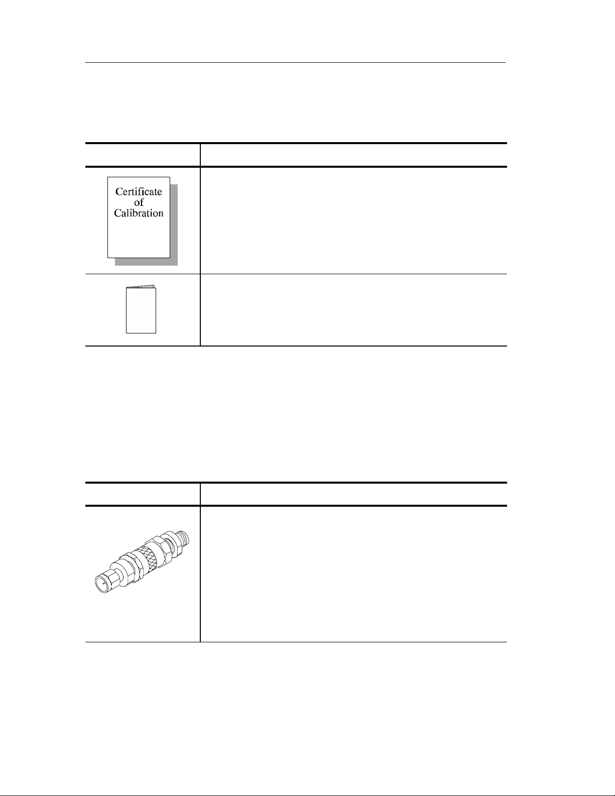
Calibration certificate. A certificate of traceable calibration is
provided with every instrument shipped.
Instruction Manual. Provides instructions for operating and
maintaining the P7380SMA differential probe.
Tektronix part number: 071-1392-XX
Optional Accessories
Table 3 shows the optional accessories that you can order for the
P7380SMA differential probe.
Table 3: Optional accessories
Accessory Description
Phase adjuster. Use two phase adjusters if you need to bring the
skew between inputs to 1 ps or less because of skew in the
device under test differential signal path. See Adjusting Cable
Skew on page 58 for instructions. The phase adjuster has a 25 ps
adjustment range.
The matched-delay SMA cables that come with your probe have a
≤1 ps skew at the cable ends.
Tektronix part number: 015-0708-XX (package of 1)
8
P7380SMA 8 GHz Differential Probe Instruction Manual
Page 25
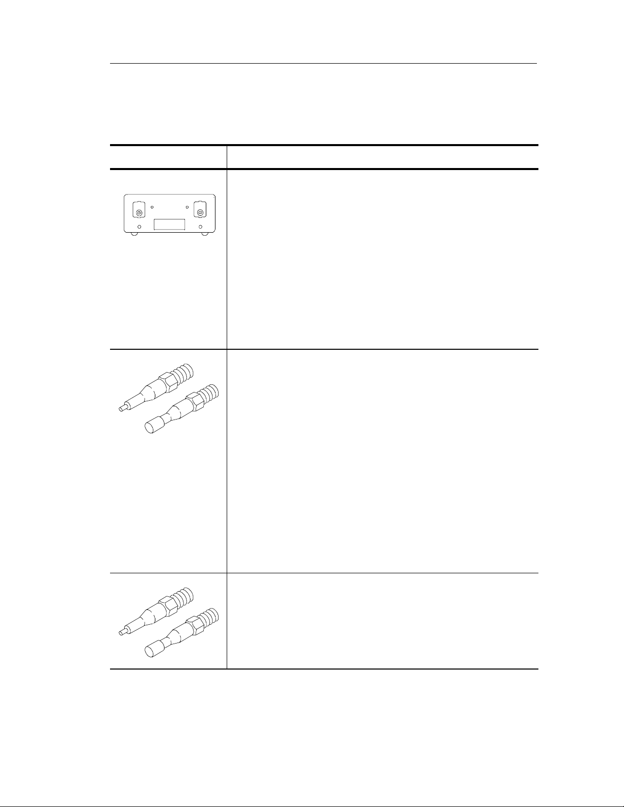
Table 3: Optional accessories (Cont.)
Accessory Description
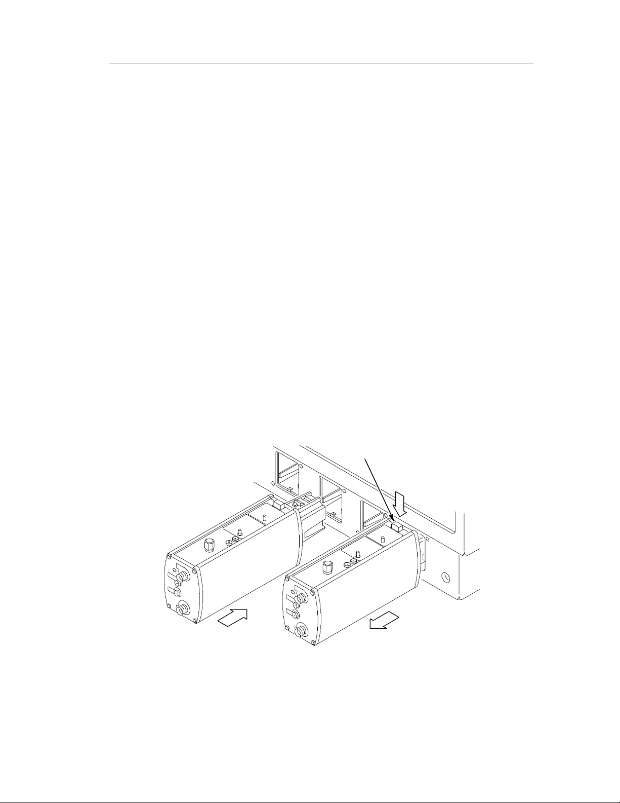
80A03. The 80A03 TekConnect Probe Interface Module is an
80A03
adapter that allows you to use TekConnect probes with CSA8000
and TDS8000 Series sampling oscilloscopes and 80E0X sampling
modules.
The interface is comprised of an enclosure that houses a
compartment for one 80E0X electrical sampling module and two
TekConnect probe inputs. The interface routes the probe signal
outputs through SMA connectors on the front panel. Semi-rigid
SMA cables link the probe outputs to the 80E0X module inputs.
The 80A03 Interface Module is required to complete a
performance verification of the probe.
Getting Started
P6150 Probe. Use the P6150 probe for checking discrete test
points in your circuit. An assortment of circuit and grounding
attachments are included to help you maintain high signal
integrity.
For best high-frequency performance, the wide-blade ground
accessory should be used with the probe tips and cut as short as
possible to connect to a ground point near the probed signal.
However, to prevent delay mismatches, do not use the cable
included with the P6150 probe. Instead, attach the tips to the ends
of the matched SMA cables that are included with the P7380SMA
probe.
Note: The P6150 probe includes (one) 1X- and (two) 10Xattenuation probe tips. If you need more tips, see P6150
Attenuation Tips below for ordering information.
P6150 Attenuator Tips. These tips attach to the ends of the
matched SMA cables that are included with the P7380SMA
probe, and are available in 1X and 10X attenuation values.
Tektronix part number: 206-0398-00 (1X Attenuation, 1 each)
Tektronix part number: 206-0399-03 (10X Attenuation, pkg of 2)
P7380SMA 8 GHz Differential Probe Instruction Manual
9
Page 26

Getting Started
Options
These options are available when ordering the P7380SMA probe:
H Option D1--Calibration Data Report
H Option D3--Calibration Data Report, 3 years (with Option C3)
H Option C3--Calibration Service 3 years
H Option D5--Calibration Data Report, 5 years (with Option C5)
H Option C5--Calibration Service 5 years
H Option R3--Repair Service 3 years
H Option R5--Repair Service 5 years
10
P7380SMA 8 GHz Differential Probe Instruction Manual
Page 27
TekConnect Interface
The P7380SMA probe is powered through a TekConnect interface
between the probe compensation box and the host instrument. The
TekConnect interface provides a communication path through
contact pins on the host instrument. Power, signal, offset, and probe
characteristic data transfer through the interface.
When the probe is connected, the host instrument reads EEPROM
information from the probe, identifying the device and allowing the
appropriate power supplies to be turned on. The preamp inputs on the
host instrument are ESD protected by remaining grounded until a
valid TekConnect device is detected.
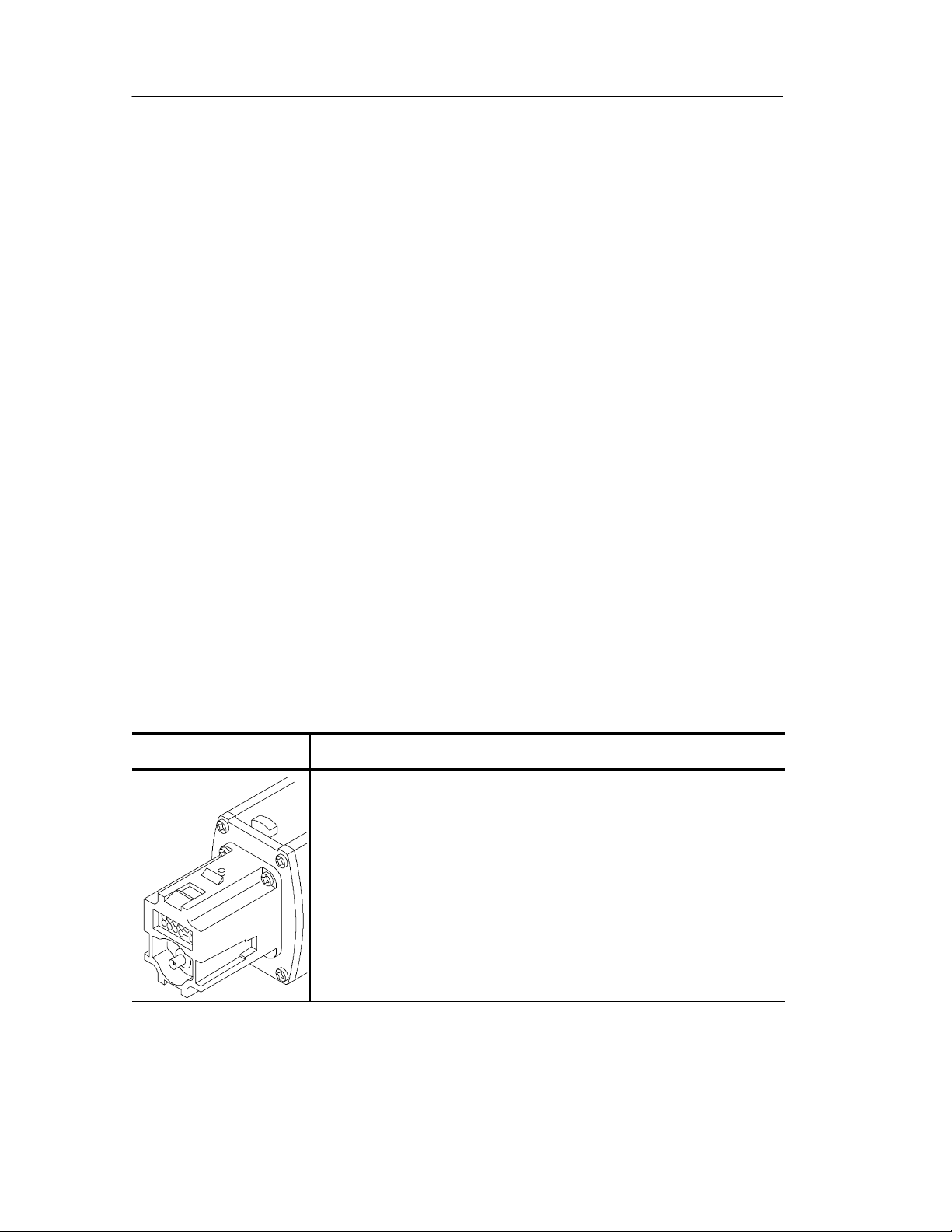
The TekConnect interface features a spring-loaded latch t hat
provides audible and tactile confirmation that a reliable connection
has been made to the host instrument. Slide the probe into the
TekConnect receptacle on the host instrument. The probe snaps into
the receptacle when fully engaged. See Figure 2.
Getting Started
To release the probe from the host instrument, grasp the compensation box, press the latch button, and pull out the probe.
Latch button
Figure 2: Connecting and disconnecting the probe
P7380SMA 8 GHz Differential Probe Instruction Manual
11
Page 28
Getting Started
Probe Inputs
The P7380SMA probe has two pairs of input connectors—one for
SMA signals and one for external DC termination voltages. Options
for the SMA input connections are shown in Figure 3.
Dual SMA cables
50 Ω
Terminations
Figure 3: Probe signal input connections
SMA Connectors
The SMA connectors provide a signal path through the internal 50 Ω
termination network and differential probe buffer amplifier to the
oscilloscope.
Use the matched-delay SMA cables that are supplied with the probe
to connect the probe to your circuit.
12
Leave the 50 Ω terminations on the unused inputs.
P7380SMA 8 GHz Differential Probe Instruction Manual
Page 29

Getting Started
DC Termination Voltage Control Jacks
Jacks are provided on the probe faceplate for external control of the
DC termination voltage, when the Vterm Source Select is set to EXT
mode. The jacks accept the 0.080 in pin-to-banana cables included
with your probe, to connect to an external power supply with banana
plug outputs.
The red terminal is the DC control voltage input to a buffer amplifier
that drives the center-tap (common-mode node) of the internal 50 Ω
termination network. The 100 KΩ resistance to ground at the buffer
amplifier input gives a 0.00V termination voltage in EXT mode with
the inputs open. The black terminal is connected to system ground.
The normal termination voltage range is ±2.5 volts. The buffer
amplifier input is diode-protected to ±15 volts, but the Overdrive
Error LED will flash when the EXT termination voltage is driven
about 10% beyond the specified ±2.5 V range. See Overdrive Error
on page 47 for more information.
Probe Input Limitations
Although the allowable input DC common mode (V
the termination voltage (V
) range are both ±2.5 V, there are
T
additional limitations on the voltage difference between V
) range and
CM
CM
and V
that you must consider, to avoid non-linear operation.
Because of the low resistance 50 Ω termination network, relatively
large currents can flow, depending on the input signal source
impedance and the V
amplifier that drives the V
and VTvoltage difference. Since the
CM
voltage node between the two 50 Ω
T
termination resistors (see Figure 15 on page 37) has a current limit of
about ±82 mA for linear operation, this limits the allowable voltage
difference between V
As a general guideline, the voltage difference between V
CM
and VT.
CM
and V
T
should be limited to about 2 V for zero-ohm source impedances and
about 4 V for 50-ohm source impedances. More exact calculations of
the termination network and input load currents can be made using
the equations in Table 5 on page 39.
T
P7380SMA 8 GHz Differential Probe Instruction Manual
13
Page 30

Getting Started
Probe Outputs
The probe provides terminals for monitoring the DC termination
voltage of the measured signal. Also, the inverted polarity of the
output signal that is passed through the TekConnect interface to the
oscilloscope is brought out to an SMA connector. These connections
are located on the top panel of the probe.
Termination Voltage Monitor Jacks
Two 0.040 in jacks allow you to monitor the termination voltage of
the signal under test, using a DMM and a pair of standard DMM test
leads. The output impedance of the termination voltage monitor (+)
output is about 1K ohm. The other output of the termination voltage
monitor is connected to signal ground.
Auxiliary Output SMA Connector
This SMA connector provides an attenuated, inverted sample of the
signal under test. The attenuation factor of the output signal m atches
the selected attenuation factor of the probe. This signal c an be used
to trigger your TDS/CSA 8000 series sampling oscilloscope, or as an
input to a spectrum- or network analyzer.
14
P7380SMA 8 GHz Differential Probe Instruction Manual
Page 31

Functional Check
Before using your probe, you should perform a functional check.
A basic functional check comprises the following:
H A power-on self test that verifies LED operation
H An input signal amplitude and termination voltage
monitor output test
If you want to check the remaining probe functions, complete the
following checks:
H Auxiliary output amplitude and polarity
H Termination voltage zero check
The equipment required for the functional checks is listed in Table 4.
Getting Started
Table 4: Equipment required for functional checks
Item description Performance requirement Recommended example
1
Oscilloscope TekConnect interface Tektronix TDS6604 or TDS7704
DMM 1.0 mV resolution Fluke 87 or equivalent
Coaxial cable Dual SMA, matched -delay 174-4944-00
Test leads 0.080 in pin-to-Banana plug
ends, one each color
Adapters (3)
SMA 50 Ω termination
012-1674-00 (red)
012-1675-00 (black)
015-1022-01
Adapter SMA short-circuit 015-1020-00
Attenuator
SMA or BNC, 50 Ω,5X
015-1002-01 (SMA)
2
2
2
3
3
011-0060-03 (BNC)
Adapter TekConnect-to-SMA Tektronix TCA-SMA
Adapter BNC Male-to-SMA Female 015-0572-00
Adapters (2) 0.040 in-to-0.080 in Pin jack 012-1676-XX
1
Nine-digit part numbers (xxx-xxxx-xx) are Tektronix part numbers.
3
3
2
Standard accessories included with the probe.
P7380SMA 8 GHz Differential Probe Instruction Manual
15
Page 32

Getting Started
Power-on Self Test
When the probe is powered on, an internal diagnostic check is
performed to verify basic probe functionality. The probe goes
through a communications check with the host instrument, and
cycles the status LEDs on the probe.
For a visual check of the probe LED functionality, connect the probe
to the oscilloscope channel you wish to use, and observe the probe
status LEDs for the following:
H All six LEDs light briefly—five on the top pane l and the
H Two LEDs light again and remain lit:
Overdrive Error LED on the front panel.
H 12.5X Attenuation
H AUTO Voltage Termination Source
The other LEDs remain unlit.
NOTE. If the Attenuation and Termination Source LEDs do not light
as described, the oscilloscope may have stored different attenuation
and termination source settings from a previous session. Use t he
SELECT buttons on the probe to toggle the LEDs to the 12.5X and
AUTO settings.
The Auto Mode LED will flash if the probe inputs are open or
AC-coupled.
If both Range Select LEDs flash or otherwise appear to be
malfunctioning after power-on, an error condition may exist. See
Appendix C: User Service for instructions on clearing errors.
Next, perform the Signal and Termination Voltage Monitor Check.
This test uses the PROBE COMPENSATION output on the front
panel of the oscilloscope to verify that the probe input circuits
function. The termination voltage monitor output is also checked,
using a DMM. Figure 4 on page 17 illustrates a typical setup.
16
P7380SMA 8 GHz Differential Probe Instruction Manual
Page 33

Getting Started
Signal and Termination Voltage Monitor Check
1. Connect the BNC--SMA adapter (included with your probe) to the
PROBE COMPENSATION connector on the oscilloscope.
2. Connect an SMA cable between the adapter and the (+) SMA
probe input. (You can use one cable of the matched-delay ca ble
set included with your probe.)
3. Connect 50 Ω SMA terminations to the (--) SMA probe input and
the Aux output connectors.
4. Set the DMM to measure DC voltage and connect it to the Vterm
monitor jacks using the 0.040 in-to-0.080 in adapters and the
0.080 in pin-to-banana plug test leads included with the probe.
The test setup is shown in Figure 4.
Probe
compensation
output
BNC-SMA
adapter
TDS6604 Oscilloscope
12.5X
AUTO
SMA cable
UseaDMMto
monitor V
0.080” Pin-to-
Banana plug cables
Ter m
Black (--)
Red (+)
DMM
0.040 in-0.080 in
Pin j ack adapters
50 Ω
Terminations
Figure 4: Signal check setup
5. Using the SELECT buttons on the probe, set the attenuation on
the probe to 12.5X, and set Vterm source to Auto.
P7380SMA 8 GHz Differential Probe Instruction Manual
17
Page 34

Getting Started
6. Press Autoset or adjust the oscilloscope to display a stable
calibration waveform. A stable square wave indicates that the
probe is functional on the 12.5X attenuation setting.
7. The probe compensation signal amplitude and common mode
voltage is dependent on oscilloscope model. Check that the signal
amplitude on the oscilloscope and the common mode voltage
(displayed on the DMM) approximate those in the table:
P7380SMA Probe
@ 12.5X Attenuation
Signal amplitude 200 mV p -p 500 mV p-p
TDS6604 TDS7704
V
CM
900 mV --250 mV
Refer to Single-Ended Measurements for more information on the
measured common mode input voltage.
This completes the 12.5X attenuation signal check. If you want to
check the 2.5X attenuation setting of the probe, do steps 8
through 11.
8. Insert a 50 Ω, 5X attenuator in-line with the probe compensation
output connector. The attenuator is necessary to bring the probe
compensation signal within the dynamic range of the probe at the
lower attenuation setting. Without this attenuator, the probe
amplifier in the 2.5X attenuator setting will be overdriven and the
display will show a limited DC level instead of the probe
compensation square wave.
You can use a BNC-style 5X attenuator, Tektronix part num-
ber 011-0060-03, or SMA-style 5X attenuator, Tektronix part
number 015-1002-01.
18
9. Set the attenuation on the probe to 2.5X.
10. Press Autoset or adjust the oscilloscope to display a stable
calibration waveform. A stable square wave indicates that the
probe is functional on the 2.5X attenuation setting.
P7380SMA 8 GHz Differential Probe Instruction Manual
Page 35

Getting Started
11. The probe compensation signal amplitude and common mode
voltage is dependent on oscilloscope model. Check that the signal
amplitude on the oscilloscope and the common mode voltage
(displayed on the DMM) approximate those in the table:
P7380SMA Probe
@ 2.5X Attenuation
Signal amplitude 40 mV p -p 100 mV p-p
TDS6604 TDS7704
V
CM
180 mV -- 5 0 m V
P7380SMA 8 GHz Differential Probe Instruction Manual
19
Page 36

Getting Started
Aux Output Check
The Aux output signal is an inverted, attenuated sample of the signal
that is displayed on the main output of the probe.
1. Set the attenuation on the probe to 12.5X.
2. Remove the 50 Ω termination from the Aux output connector.
3. Connect an SMA cable from the probe Aux output to another
channel on the oscilloscope, using a Tektronix TCA-SMA
adapter. See Figure 5 for the test setup. (You can use the other
cable of the matched-delay cable set included with your probe.)
TDS6604 Oscilloscope
UseaDMMto
monitor V
Ter m
DMM
Probe
compensation
output
BNC-SMA
adapter
Figure 5: Aux output check test setup
TCA-SMA
adapter
Black (--)
Red (+)
0.04 in-0.080 in
Pin j ack adapters
50 Ω
Termination
SMA cables (can be
matched-delay set)
20
P7380SMA 8 GHz Differential Probe Instruction Manual
Page 37

Getting Started
4. Display the channel that you connected the Aux Output signal to,
and check that the Aux Output signal is an inverted sample of the
probe compensation signal that is displayed on the P7380SMA
main output.
Also note that the Aux Output amplitude is attenuated by a factor
of 12.5X from that displayed on the P7380SMA main output.
This is a result of the intelligent probe interface that adjusts for
the selected attenuation factor on the main probe output.
This completes the 12.5X attenuation Aux Output signal check.
If you want to check the 2.5X attenuation setting of the probe, do
step 5. Note: This check requires the 5X external attenuator as
describedinstep8onpage18.
Due to the combination of the 5X attenuator and the 5X increase in
the probe gain (from 12.5X to 2.5X), the amplitude of the measured
signal in the 2.5X attenuation check in step 5 will match that of the
12.5X attenuation check in step 4.
5. Insert a 50 Ω, 5X attenuator in-line with the probe compensation
output connector, set the attenuation on the probe to 2.5X and
check that the signal amplitude is the same as in step 4.
P7380SMA 8 GHz Differential Probe Instruction Manual
21
Page 38

Getting Started
DC Termination Voltage Zero Check
This test checks that the termination voltage defaults to 0 volts under
the conditions shown below for the three different termination
voltage selection modes.
Auto Mode.
1. Disconnect the SMA cables from the (+) input of the probe and
the Aux output connector.
2. Connect 50 Ω SMA terminations to the (+) input of the probe and
the Aux output connector.
3. Leave the 50 Ω SMA termination connected to the (--) input.
The test setup is shown in Figure 6 on page 22.
4. Use the Vterm SELECT button on the probe to set the Vterm
mode to AUTO. Check that the DMM displays the termination
voltage of approximately 0 V.
TDS6604 Oscilloscope
UseaDMMto
monitor V
Ter m
Black (--)
Red (+)
DMM
0.040 in-0.080 in
Pin j ack adapters
50 Ω
Terminations
Figure 6: DC termination voltage check setup
22
P7380SMA 8 GHz Differential Probe Instruction Manual
Page 39

Getting Started
Int Mode.
5. Use the Vterm SELECT button on the probe to set the Vterm
mode to INT.
The DMM should display the termination voltage of approximately 0 V. If not, check that the oscilloscope has an internal
Vterm control set to a voltage other than zero. See your
oscilloscope manual for details on using the internal Vterm
controls.
Ext Mode.
6. Verify that the external termination voltage inputs on the probe
are open.
7. Use the Vterm SELECT button on the probe to set the Vterm
mode to EXT. Check that the DMM displays the termination
voltage of approximately 0 V.
This completes the functional check of the probe. If your instrument
supports probe calibration routines, now is a good time to perform
them. See Probe Calibration on page 24 for instructions.
P7380SMA 8 GHz Differential Probe Instruction Manual
23
Page 40

Getting Started
Probe Calibration
After you perform a functional check of the probe, run a probe
calibration routine. The purpose of calibrating the probe is to
optimize the gain and offset of the probe and oscilloscope combination to minimize measurement errors.
The Calibration Status of the instrument Signal Path Compensation
test must be pass for the probe calibration routine to run:
1. From the Utilities menu, select Instrument Calibration.
2. In the Calibration box, check tha t the Status field is pass.Ifitis
not, disconnect all probes and signal sources from the oscillo-
scope, and run the Signal Path Compensation routine.
When the Signal Path Compensation test status is pass, run the probe
calibration routine:
3. Connect the probe to one of the oscilloscope channels, and set the
oscilloscope to display the channel. Allow the probe to warm up
for 20 minutes.
4. Connect the SMA cable from the PROBE COMPENSAT ION
connector on the oscilloscope to the (+) SMA probe input.
NOTE. Some oscilloscopes, such as the TDS6804B, have a separate
Probe Cal output rather than the Probe Compensation output for
probe calibration.
For probe calibration with a TDS6804B oscilloscope, or other
models that have a separate Probe Cal output, a BNC-SMA adapter
should be attached to the Probe Cal output and the + SMA probe
cable input should be connected to the adapter.
5. Connect a short-circuit SMA termination to the (--) input of the
probe.
The test setup is shown in Figure 7 on page 25.
24
P7380SMA 8 GHz Differential Probe Instruction Manual
Page 41

Probe
compensation
output
Getting Started
TDS6604 Oscilloscope
BNC-SMA
adapter
SMA cable
SMA short-circuit
50 Ω
Termination
Figure 7: Probe calibration setup
6. From the Vertical menu, select Probe Cal.
7. Press or click Calibrate probe.
The probe calibration routine runs, optimizing the probe to the
oscilloscope for both probe attenuation settings.
After the probe passes the functional checks and probe calibration
routine, you can use the probe in your measurement system. If your
probe fails the functional checks or probe calibration routine, see
Appendix C: User Service.
You can use the probe to make both single-ended and differential
measurements. The following pages show some of the ways that you
can use your probe.
P7380SMA 8 GHz Differential Probe Instruction Manual
25
Page 42

Getting Started
Using the Probe
The termination voltage control modes allow you to monitor and/or
control the termination voltage using three different methods. If you
are using a second measurement instrument, such as a spectrum
analyzer, the auxiliary output provides an attenuated, inverted
sample of the input signal for a dditional processing. The fol lowing
figures illustrate some typical probe configurations and applications.
Auto Mode
Figure 8 shows the probe connections for testing 50 Ω serial data
lines, such as InfiniBand or PCI Express. In this example, Auto mode
is used to automatically set the termination voltage. By matching the
termination voltage to the input signal common mode voltage, Auto
mode minimizes the DC loading on the differential input source.
TDS6604 Oscilloscope
AUTO mode
Note: To make DUT connections
easier, connect the phase-adjuster
ends of the cables to the probe.
Optional: Use a DMM
to monitor V
Ter m
Black (--)
Red (+)
DMM
0.040 in-0.080 in
Pin j ack adapters
50 Ω Termination
on Aux Out
To circuit
under test
Figure 8: Using Auto Termination Voltage Control Mode
26
P7380SMA 8 GHz Differential Probe Instruction Manual
Page 43
Getting Started
External Mode
For applications where you want to control the termination voltage,
set the Vterm source to Ext mode and connect the termination
voltage control inputs to an external power supply, as shown in
Figure 9. You can use a DMM to verify that the termination voltage
matches the externally-supplied DC control voltage.
TDS6604 Oscilloscope
EXT mode
External DC termination voltage
control input terminals
0.080” Pin-toBanana plug cables
Black (--)
Red (+)
UseaDMMto
monitor VTerm
DMM
0.040 in-0.080 in
Pin j ack adapters
50 Ω term
on Aux Out
Black (--)
Use external
DC supply to
control VTerm
Power supply
+
--
Red (+)
Figure 9: Using External Termination Voltage Control Mode
P7380SMA 8 GHz Differential Probe Instruction Manual
To circuit
under test
27
Page 44

Getting Started
Internal Mode
For TekConnect-interface oscilloscopes that support Int mode, you
can use this feature to generate termination voltages with the
oscilloscope, using the graphical user interface. This eliminates the
need for an external power supply. Figure 10 shows the setup.
Refer to your oscilloscope manual for details on using the interface.
TDS6604 Oscilloscope
UseaDMMto
monitor V
Ter m
DMM
INT mode
Black (--)
Red (+)
0.040 in-0.080 in
Pin j ack adapters
50 Ω Termination
on Aux Out
To circuit
under test
Figure 10: Using Internal Termination Voltage Control Mode
28
P7380SMA 8 GHz Differential Probe Instruction Manual
Page 45

Getting Started
Auxiliary Output
The Aux out connection can be used to connect to a spectrum or
network analyzer, or for generating clock recovery signals used for
other instrumentation. See Figure 11.
TDS6604 Oscilloscope
Spectrum Analyzer
RF input
To circuit
under test
SMA cable
Aux Out
Figure 11: Viewing the Aux Out signal on a spectrum analyzer
P7380SMA 8 GHz Differential Probe Instruction Manual
29
Page 46

Getting Started
Using the Probe With a Sampling Oscilloscope
You can use the P7380SMA probe with Tektronix TDS/CSA8000
Series sampling oscilloscopes, using the Tektronix 80A03 TekConnect Probe Interface. The 80A03 interface is an optional accessory
for the probe that adapts TekConnect probes to 8000 Series
oscilloscopes.
The 80A03 interface uses 80E0X Series electrical modules that are
part of the Tektronix 8000 Series oscilloscope family.
NOTE. The firmware of your 80A03 interface must be version 1.2 or
higher to be compatible with your P7380SMA probe.
80A05 Clock Recovery Module.
By adding an 80A05 Clock Recovery Module to your sampling
oscilloscope, you can use the Aux output of your P7380SMA probe
to trigger the module on the input signal and view eye diagrams. The
80A05 module generates a recovered clock from an acquired data
stream when the data rate is known. Figure 12 on page 31 shows a
test setup.
If a clock signal rather than a data signal is acquired by the probe,
then the Aux output can be connected to one of the oscilloscope
external trigger inputs.
30
P7380SMA 8 GHz Differential Probe Instruction Manual
Page 47

TDS/CSA8000 Series Oscilloscope
Getting Started
80A03 TekConnect
Probe Interface
80A03
Data input
80A05 module
SMA cable
Circuit under
test
Dual SMA cables
80E0X module
Aux Out
Figure 12: Using the probe with an 80A03 Interface and an 80A05
Module to view eye diagrams on a TDS8000 Series sampling oscilloscope
P7380SMA 8 GHz Differential Probe Instruction Manual
31
Page 48
Getting Started
P6150 Probe Tips
The P6150 probe is an optional accessory for the P7380SMA
differential probe. The low-capacitance probe tips included with the
P6150 probe provide a way for you to take measurements from test
points other than SMA connectors.
For best results, use the matched SMA cable set include d with your
P7380SMA probe to connect between the P7380SMA probe and the
P6150 probe tips.
Be aware of the tradeoffs between dynam ic range and noise when
using the 10X probe tips with the attenuation set at 12.5X. Also note
that the vertical scale of the oscilloscope will be off by a factor of 10
when using the 10X tips.
1X
10X
Figure 13: P6150 probe tips
To the
probe
32
If you need to probe two points that are farther apart than the
matched SMA cable set will allow, only use matched, high-quality,
low loss SMA cables, and deskew them before attaching the probe
tips. See Checking Cable Skew on page 57 for instructions.
P7380SMA 8 GHz Differential Probe Instruction Manual
Page 49

Operating Basics
This section discusses differential measurements using an SMA i nput
probe for Serial Data compliance testing. It also provides information on the probe architecture and operation details to aid in its
proper application.
Differential Measurements for Serial Data Compliance Testing
Differential Signalling
Gigabit serial data signals are commonly transmitted using
differential signaling techniques because of improved signal fidelity
and noise immunity. Although the physical layer specifications differ
somewhat between the different gigabit serial data communication
standards, they have some common elements. Most gigabit seri al
data signals are transmitted over 50 Ω transmission lines which are
terminated at both ends of a point-to-point differential interconnect.
The signal transmitter provides a 50 Ω source impedance from each
of its two differential outputs and the signal receiver provides an
effective 50 Ω input impedance on each of its two differential inputs.
The two complementary single-ended signals that comprise the
differential signal are generally offset from ground at a commonmode voltage level, which allows the use of unipolar transmitters and
receivers that are powered from a single power supply voltage. The
transmitted signals are usually encoded using a DC-balanced
encoding technique that allows the signals to be either AC or DC
coupled in the transmission path. If DC coupled, the receiver
termination must generally be terminated to the same DC common-mode voltage as the transmitter, to reduce DC loading on the
transmitter output. An example of the single-ended signals
transmitted by an InfiniBand standard driver and the resultant
differential signal that would be measured by a differential
measurement system is shown in Figure 27 on page 64.
P7380SMA 8 GHz Differential Probe Instruction Manual
33
Page 50

Operating Basics
Although the differential response is generally the primary
measurement of interest for a differential signal, full characterization
of the signal also requires measurement of the single-ended response
of the two complementary signals including the DC common-mode
voltage.
Pseudo-Differential Measurements
A common differential measurement technique uses two singleended probes or direct connection to two oscilloscope channels for
the differential signal capture. By calculating the difference between
the two input signals using waveform math, the effective differential
signal seen by a differential receiver can be displayed for analysis.
This measurement technique, which is commonly refered to as
pseudo-differential measurement, has a number of limitations when
compared to the use of a differential probe like the P7380SMA. In
addition to the obvious overhead of two oscilloscope channels for the
measurement instead of the single channel needed by a differential
probe, there are a number of additional problems.
Unlike the differential probe, which has been carefully designed with
short, matched-input signal paths, a pseudo-differential measurement
uses two oscilloscope channels which are physically separated and
generally not matched as well. Although it is possible to deskew the
timing differences between two high performance oscilloscope
channels to improve the accuracy of a pseudo-differential measurement, deskewing is a relatively involved procedure that may need to
be repeated if any oscilloscope parameter, such as vertical gain, is
changed.
The gain match between two different oscilloscope channels is also a
potential problem, particularly at higher frequencies where channel
gain mismatch can contribute to significantly reduced CMRR
performance. The CMRR performance of a differential probe, on the
other hand, is generally much better controlled, with fully characterized specifications over the full probe bandwidth.
The requirement of generating a math waveform for display of the
differential signal in a pseudo-differential measurement can also
introduce some subtle problems with waveform analysis, since some
features such as COMM triggering or mask testing may not be fully
supported with math waveforms. The use of a differentia l SMA-input
34
P7380SMA 8 GHz Differential Probe Instruction Manual
Page 51

Operating Basics
probe like the P7380SMA also provides additional features like
adjustable termination voltage that may be very useful in fully
characterizing the performance of differential data transmitters. High
performance oscilloscope channels are almost always limited to zero
volt termination voltage, since the oscilloscope termination resistor
is connected directly to signal ground.
Differential Probe Measurements
A differential probe is designed to provide a differential input
interface for a single-ended oscilloscope channel. It includes a
carefully matched differential signal input path and a differential
buffer amplifier.
A conventional differential probe input generally has a high DC
input resistance and as small an input loading capacitance as
possible. The light input loading of a conventional differential probe
is designed to perturb the circuit being measured as little as possible
when the probe is attached.
An SMA-input probe like the P7380SMA has a very different input
structure. It has a dual, matched 50 Ω input that is designed to
terminate the measured signal transmission path with minimum
reflections. It is designed specifically for serial compliance testing.
Its SMA input connectors provide a reliable, repeatable interconnect
for making accurate eye pattern measurements that are used to
characterize the quality of a serial data transmission channel.
The P7380SMA probe has also been carefully designed for flat
amplitude response and very small pulse response aberrations. This
helps to ensure accurate eye pattern measurements over a wide data
rate range.
The differential amplifier (see Figure 14 on page 36) is at the heart
of any device or system designed to make differential measurements.
Ideally, the differential amplifier rejects any voltage that is common
to the inputs and amplifies any difference between the i nputs.
Voltage that is common to bot h inputs is often referred to as the
Common-Mode Voltage (V
Differential-Mode Voltage (V
) and difference voltage as the
CM
).
DM
The simplified input signal voltage source model driving the
differential amplifier in Figure 14 shows a complementary
P7380SMA 8 GHz Differential Probe Instruction Manual
35
Page 52

Operating Basics
differential signal without source or termination impedance. In a
real-world measurement, the signal source and measurement
termination impedance must be known and included in the
measurement analysis.
The model in Figure 14 also shows that the output from the
differential amplifier has twice the peak-to-peak amplitude of each
complementary input signal.
+
V
CM
+
=
V
DM
--
+
V
DM
+
A
--
V
DM
out
2A
DMVDM
V
out
--
--
Figure 14: Simplified model of a differential amplifier
Common- Mode Rejection Ratio
In reality, differential amplifiers cannot re ject all of the commonmode signal. The ability of a differential amplifier to reject the
common-mode signal is expressed as the Common-Mode Rejection
Ratio (CMRR). The CMRR is the differential-mode gain (A
divided by the common-mode gain (A
). It is expressed either as a
CM
DM
)
ratio or in dB.
A
DM
A
CM
CMRR =
A
DM
CMRR(dB) = 20 log
A
CM
36
CMRR generally is highest (best) at DC and degrades with
increasing frequency.
P7380SMA 8 GHz Differential Probe Instruction Manual
Page 53

Figure 28 on page 68 shows the typical CMRR response of the
P7380SMA differential probe over frequency. High CMRR in a
differential probe requires careful matching of the two input paths.
Poorly matched signal source impedances can significantly degrade
the CMRR of a measurement. Mismatches between the two
differential signal input paths result in an effective conversion of
to VDM, which reduces the CMRR.
V
CM
Probe Block Diagram (Simplified)
The SMA inputs and probe termination network provide a hi g h
frequency, 50 Ω signal path to the internal probe amplifier. The use
of SMA-female connectors provides a reliable, repeatable attachment
method for input signals. The symmetry of the input termination
network is designed to reduce skew and maximize CMRR.
Operating Basics
A simplified schematic of the P7380SMA input termination network
is shown in Figure 15.
IN +
50
Delay-matched
cable pair
V
T
50 Ω
Ω
Attenuator and
VCM
Compensation
IN --
Scope
+
-Aux Out
Figure 15: Input termination network
Matched-Delay Cables
The standard delay-matched cables for the P7380SMA differential
probe have been carefully designed to provide guaranteed probe
P7380SMA 8 GHz Differential Probe Instruction Manual
37
Page 54

Operating Basics
performance at the SMA connector interface on the end of the cable.
The delay between the two matched cables in the standard cable
assembly is adjusted to provide an initial skew of less than 1 ps.
Cable skew this small can be degraded by cable flexure and through
other environmental factors. Care should be taken to minimize
physical mishandling of this quality cable assembly to preserve
probe performance.
The cable used in the standard cable assembly has also been selected
for its low-loss characteristics, and the cable length was selected to
match the cable loss compensation designed into the probe
differential amplifier. If an alternative cable assembly is used in
measurements with the P7380SMA differential probe amplifier, this
loss compensation characteristic must be considered. The following
approximate equation for cable loss compensation c an be used as a
guideline in custom cable designs and is valid over a frequency range
of about 1 GHz to 8 GHz:
Loss = 0.5dB + 0.15dB *(F − 1), where F is frequency in GHz
Custom cable pairs must also be designed with very low skew or the
skew must be minimized using a pair of adjustable phase trimmer
adapters like those listed in the Opti onal Accessories on page 8.
Input Termination Network
The input termination network in the P7380SMA differential probe
includes a pair of laser trimmed 50 Ω termination resistors,
,is
in
T
connected together at a common--mode voltage node, labe led V
Figure 15. The common--mode termination voltage node, V
T
designed to provide a broadband, low impedance termination for
input common--mode signals. The probe termination voltage can be
adjusted using several different modes that will be described later.
The termination voltage range is ±2.5 V, which matches the
allowable input signal common--mode voltage range. For DCcoupled serial data signals, the termination voltage, V
, should
T
generally be set to equal the input signal common--mode voltage,
V
; for AC-coupled serial data signals, the termination voltage, VT,
CM
should generally be set to 0 V.
38
P7380SMA 8 GHz Differential Probe Instruction Manual
Page 55

Operating Basics
The adjustability of the termination voltage also provides measurement flexibility for characterizing or stressing serial data signal
drivers. Because of the low impedance of the input termination and
attenuator network, the signal termination currents can become quite
large. Table 5 below can be used to calculate the DC common--mode
voltages and currents at the probe inputs and termination voltage
driver under several common source impedance conditions.
Table 5: Common- mode voltage and current table
Source impedance
1
0 Ω 50 Ω
VIV
I
I
1
CM
40.00 mA x VT-- 40.00 mA x V
I
40.00 mA x VT-- 23.33 mA x V
T
CM
CM
When inputs are AC coupled: VI=VT,II=0,IT= 16.67 mA x V
0.5 x (VT+VCM)
20.00 mA x VT-- 20.00 mA x V
28.33 mA x VT-- 1 1 . 6 7 m A x V
T
CM
CM
The probe block diagram shows that the input termination network is
followed by an attenuator and V
compensation circuit. The
CM
attenuator is used to increase the effective input dynamic range of
the probe differential amplifier.
The P7380SMA probe has two attenuation settings, 2.5X and 12.5X,
that allow dynamic range to be traded off against signal noise. The
12.5X attenuator setting has the largest dynamic range; the 2.5X
attenuator setting has the lowest noise.
The V
compensation circuit automatically minimizes the DC
CM
common--mode voltage at the probe different ial amplifier inputs
even with varying termination voltage and input signal DC
common--mode voltage. This maximizes the differential mode signal
input dynamic range. The V
compensation circuit allows the DC
CM
common--mode input voltage range to be the same for both
attenuator settings as shown in Figure 17 on page 43.
P7380SMA 8 GHz Differential Probe Instruction Manual
39
Page 56

Operating Basics
Internal Probe Amplifier
The P7380SMA differential probe is designed to measure high
frequency, low-voltage circuits. Before connecting the probe to your
circuit, take into account the limits for maximum input voltage, the
common-mode signal range, and the differential-mode signal range.
For specific limits of these parameters, see Figure 17 on page 43 and
Specifications startingonpage65.
Maximum Input Voltage.
The maximum input voltage is the maximum voltage to ground that
the inputs can withstand without damaging the probe input circuitry.
CAUTION. To avoid damaging the inputs of the P7380SMA differential probe, do not apply more than ±5 V (DC + peak AC) between
each input and ground. In addition, the maximum termination
resistor power must not be exceeded to avoid probe damage.
Maximum Termination Resistor Power.
The internal termination resistors can safely dissipate 0.2 W of
power continuously, which is the case for normal probe operation
without termination driver current overload. However, the probe will
be damaged if you apply more than 0.5 W of power through the
termination resistors for more than 5 minutes.
If you suspect your measurement application will approach these
limits, use the formulas that follow to calculate the power dissipated
by the termination resistors.
The power calculation formulas are based on the simplified model
shown in Figure 16 on page 42, which represents the signal at the
probe inputs. If a signal source with 50 Ω source impedances is used,
the signal levels used should match the zero-ohm source impedance
model in Figure 16.
40
P7380SMA 8 GHz Differential Probe Instruction Manual
Page 57

Operating Basics
V
V
CM
DM(p-p)
DC power =
AC power =
VCM− V
Ꮑ
V
DM(p−p)
Ꮑ
100
50
T
Ꮖ
(VCM− VT) per side
V
DM(p−p)
ᏆᏁ
Ꮖ
2
per side
The signal source model defined for these equations is as follows:
V+and V−=
V+= VCM+ V
Single-ended signals i nto a 50 Ω load
V
= VCM− V
DM
−
DM
This results in the terms to be used in the power equations above:
VCM=
+ V
V
+
−
2
V
=
DM
− V
V
+
−
2
VT= Termination input voltage
Note: With a balanced DC signal, in the equations above,
V
is half of the value of a conventional differential signal.
DM
V
= V+− V−= 2V
diff
DM
P7380SMA 8 GHz Differential Probe Instruction Manual
41
Page 58

Operating Basics
〈±5.0 V
V+
+
V
DM
maximum)
50 Ω
--
+
V
CM
--
+
V
DM
--
-- VT| < 5V
|V
+
|V
-- VT| < 5V
--
50 Ω
〈±5.0 V
V--
maximum)
V
T
Figure 16: Probe maximum input limits
Common-Mode Signal Range.
The common-mode signal range is the maximum voltage that you
can apply to each input, with respect to earth ground, without
saturating the input circuitry of the probe. A common-mode voltage
that exceeds the common-mode signal range may produce an
erroneous output waveform even when the differential-mode
specification is met.
Differential-Mode Signal Range.
42
The differential-mode signal range is the maximum voltage
difference between the plus and minus inputs that the probe can
accept without distorting the signal. The distortion from a voltage
that is too large can result in a clipped or otherwise distorted and
inaccurate measurement. The differential mode signal range is
dependent on the probe attenuator setting as shown in Figure 17 on
page 43.
For a more detailed description of the differential mode dynamic
range, see Differential Measurement Topology on page 48.
P7380SMA 8 GHz Differential Probe Instruction Manual
Page 59

Operating Basics
12.5X
Range
+2.50 V
+1.50 V
0V
--1.50 V
--2.50 V
Nonoperating range (+5 V maximum nondestructive input voltage )
+Sig
-- S i g
V
CM
Differential Mode Range
Nonoperating range (--5 V maximum nondestructive input voltage )
Common Mode Range
Figure 17: Differential and Common-Mode operating ranges
2.5X
Range
+2.50 V
+312 mV
0V
--312 mV
--2.50 V
Common-Mode Rejection.
The common-mode rejection ratio (CMRR) is the ability of a probe
to reject signals that are common to both inputs. More precisely,
CMRR is the ratio of the differential-mode gain to the commonmode gain. The higher the ratio, the greater the ability to reject
common-mode signals. For additional information about CMRR, see
page 36.
Probe Amplifier Outputs.
The P7380SMA probe has a differential signal output. The positive
polarity output is connected to the oscilloscope through the
TekConnect probe interface. The inverted polarity output is
connected to the Aux Output SMA connector on the top of the probe.
The positive polarity main output is automaticlly scaled by the
intelligent TekConnect probe interface to compensate for probe
attenuation and display the differential signal voltage at the probe
inputs. The inverted Aux Output is an attenuated version of the
differential signal input, which must be manually ac counted for in
signal measurements or processing.
P7380SMA 8 GHz Differential Probe Instruction Manual
43
Page 60

Operating Basics
Termination Voltage Control
The P7380SMA probe termination voltage can be controlled either
internally or externally, as selected by three different modes. A block
diagram of the probe termination network is shown in Figure 18
below. A discussion of the circuitry follows.
INT
V
TERM
EXT
V
TERM
Input
GEN
100K
INT
mode
EXT
mode
V
TERM
Driver
V
TERM
Monitor
AUTO
V
TERM
GEN
AUTO
mode
Figure 18: Termination voltage network drive
The P7380SMA probe has been designed for compliance testing of
high-speed, serial data standards such as PCI Express, InfiniBand,
SerialATA, XAUI, Gigabit Ethernet, Fibre Channel, and others. All
of these high--speed, differential data standards define a common-mode voltage less than the ±2.5 V termination range of the
P7380SMA probe.
The probe termination voltage can be set to the desired input signal
common--mode voltage using one of three control modes: Auto, the
default mode at power-on, Internal, and External. The operation of
these modes are described below.
44
P7380SMA 8 GHz Differential Probe Instruction Manual
Page 61
Operating Basics
Auto Mode
When the probe is first connected to the oscilloscope, a self test runs,
and the default termination voltage control mode is set to Auto.
When the probe is in Auto mode, the common--mode voltage of the
input signal is monitored, and the DC termination voltage is set to
match the common--mode input voltage. Auto mode provides the
minimum DC loading on the input signal source.
With open inputs or a high DC source impedance, such as an
AC-coupled input signal, the Auto mode select LED flashes,
indicating that the termination voltage has been set to zero volts.
This is the mode that you will likely use for most compliance testing
of current serial data standards.
Int Mode
The internal mode allows you to set the termination voltage with
user controls available on some TekConnect-interface oscilloscopes.
You can adjust the DC termination voltage within the ±2.5 V range.
See your oscilloscope manual for details on using this mode.
Ext Mode
When the probe is in external mode, it allows control of the DC
termination voltage with an external power supply. You can adjust
the DC termination voltage within the ±2.5 V termination voltage
range of the probe.
The external DC termination voltage control input is buffered by an
internal amplifier with 100 K ohm input impedance.
WARNING. Do not exceed the ±15 V external mode voltage maximum
for the probe. Excess voltage will damage the probe.
In Ext mode, the external DC voltage is connected to the red (+) and
black ( --) terminals on the end of the probe head, which accept
standard 80 mm plugs. A pair of 0.080 in-to-banana plug adapter
cables are included with the probe for making connections from
these connectors to external power sources. The black terminal is
ground and is connected to the outer case of the shielded module that
holds the SMA input terminals. When you are not using these
P7380SMA 8 GHz Differential Probe Instruction Manual
45
Page 62

Operating Basics
terminals, they can be left open and unconnected. When the Ext
mode input terminals are left open, the Ext mode termination voltage
defaults to 0.0 V.
The termination voltage supplied to the input termination network by
the Vterm driver can be monitored with a DMM on a pair of
0.040 inch pin jacks on the top of the probe. This allows you to
verify the termination voltage setting, and when you are using Auto
mode, allows you to measure the common--mode input voltage.
You can use a pair of 0.040 inch-to-0.080 inch pin jack adapters with
the 0.080 inch-to-banana plug cables (both are standard accessories
included with your probe), to make a more permanent connection to
the monitoring DMM.
46
P7380SMA 8 GHz Differential Probe Instruction Manual
Page 63

Overdrive Error
The P7380SMA differential probe can measure signals that have a
common--mode voltage range of ±2.5 V. Although the termination
voltage range is also specified to be ±2.5 V, limitations on the linear
current range of the termination voltage driver restrict the voltage
difference between V
Generally, you must keep the termination voltage within about
2.5 volts of the common--mode voltage, or the Overdrive Error LED
will glow solid, indicating an over-current situation, which may lead
to a measurement error.
CM
Operating Basics
and VT.
The specific voltage difference between V
both the source impedance and the V
CM
and VTis dependent on
CM
and VTvalues. You can use
the input termination network table on page 39 t o determine
allowable conditions, with the Overdrive Error current threshold for
set at about ±80 mA.
I
T
The Overdrive Error LED will also flash red when the termination
voltage exceeds the allowable ±2.5 volt range. This can occur in
Auto mode when V
mode when the V
exceeds a threshold of about ±2.8 V, or in Ext
CM
input voltage exceeds the same threshold. If this
T
occurs, remove all signal sources from the probe to clear this LED.
The Overdrive Error LED provides an active status monitor of error
conditions; it does not latch and store the occurence of an error
condition.
Overdrive error indicator LED
Figure 19: Overdrive Error indicator
P7380SMA 8 GHz Differential Probe Instruction Manual
47
Page 64

Operating Basics
Differential and Single-Ended Signal Measurement
Although designed for differential signal measurement, the
P7380SMA probe can be used to make single-ended measurements
when properly configured. The analysis that follows describes some
differential and single-ended measurements of typical high-speed
serial data signals.
Differential Measurement Topology
A typical differential measurement topology using the P7380SMA
probe is shown in Figure 20. The termination network for the probe
in this figure includes a termination capacitor. This is intended to
show that the termination network provides a broadband AC ground
for common--mode signals.
IN +
IN --
50 Ω
V
50 Ω
V
IP
Atten
T
&V
CM
comp
V
IN
V+
V--
V out
+
--
±V
V
±V
DM
CM
DM
50 Ω
+
-+
--
50 Ω
Figure 20: Differential measurement topology
Although an ideal differential signal is theoretically terminated at the
V
node due to symmetry, the low impedance VTnode terminates
T
any non-ideal, AC common--mode signal components. The input
signal source model includes a common--mode component, V
complementary differential mode components, ±V
DM
.
CM
,and
48
The differential mode signal source models have double the signal
amplitude of the measured signal at each input because of the 50 Ω
voltage divider between the source and termination resistance.
P7380SMA 8 GHz Differential Probe Instruction Manual
Page 65

Operating Basics
The common--mode signal source model does not have double the
signal source amplitude because most serial data transmitters are
designed to drive a load resistance terminated with the DC
common--mode voltage, not signal ground.
With V
mode voltage at each probe input should equal V
setequaltoVCMin this model topology, the DC common--
T
. The resulting
CM
differential signals at the probe inputs are:
VIP= VCM+ V
DM
VIN= VCM− V
DM
The attenuator and VCMcompensation network that follows the
termination network nulls out the V
signal and attenuates the V
CM
DM
signals. The resulting differential signals at the probe amplifier
inputs for a 2.5X attenuation setting are:
V+= 0.4V
DM
V−=−0.4V
DM
The resulting output signal from the probe output is:
V
=−0.8V
out
DM
The inverted polarity of the probe amplifier output can be verified by
examining the probe Aux Output signal. The main probe output
signal is routed through the TekConnect interface connector and is
automatically scaled to show the correct differential amplitude at the
probe input connectors.
Differential Dynamic Range
The V
compensation circuit in the probe attenuator is designed to
CM
maximize the dynamic range of the AC component of the input
signal. For most high-speed serial data signals, the AC component of
the signal is of most interest for compliance testing where an eye
pattern display of the differential signal is checked for timing jitter
and voltage amplitude and fidelity.
The DC common--mode component of the input signal is present
primarily to bias the signal into the operating range of the receiver
and may even be removed in the transmission path with AC coupling. The V
compensation circuit in the P7380SMA probe is
CM
designed to null out the DC common--mode component of the input
P7380SMA 8 GHz Differential Probe Instruction Manual
49
Page 66

Operating Basics
signal, V
, so that only the differential mode component of the
CM
input signal is passed through to the probe amplifier inputs.
The V
compensation circuit allows the dynamic range of the
CM
probe to be specified as a differential peak-to-peak voltage with a
separate DC common--mode range. The differential peak-to-peak
voltage specification is different for the two probe attenuation
settings, but the DC common--mode range is the same for both
attenuation settings.
The DC common--mode range of the probe is actually describing the
performance of the V
compensation circuit, rather than the
CM
dynamic range of the probe amplifier. The dynamic range of the
probe has been specified as a differential peak-to-peak voltage
because that best represents the way in which the signal is typically
displayed and specified for compliance testing.
Single-Ended Measurement Topology
Although the P7380SMA differential probe can be used to make
single-ended measurements, it is important to understand the impact
of the termination network on the measured response, particularly on
the DC common--mode component of the signal.
Because of the limited dynamic range of the probe amplifier,
single-ended measurements, which also display the DC common-mode component of the signal, must be carefully checked for
possible overdrive problems. The single-ended measurement
topology can also affect the performance of Auto mode, which will
only function properly with a matched source impedance configuration.
Three possible single-ended measurement topologies will be
examined in this section. They differ in the termination used on the
(--) input of the probe when the single-ended signal is connected to
the (+) input.
50
P7380SMA 8 GHz Differential Probe Instruction Manual
Page 67

Operating Basics
50 Ohm Termination on (--) Input.
A single-ended measurement topology with a 50 Ω termination on
the probe input is shown in Figure 21. The general equations that
describe the response of that topology are also shown, incl uding DC
loading on the signal source.
50 Ω
+
±V
DM
V
CM
DC loading on VCMsource:
--
50 Ω
=
I
L
IN +
50 Ω
50 Ω
IN --
V
− V
CM
IP
50
V
IP
V
T
V
IN
VIP=
V
Figure 21: 50 ohm termination on (- ) input
AV= 0.40 for 2.5X
= 0.08 for 12.5X
Atten
&V
CM
comp
V
V
=
IN
2
VO= (VIP− VIN)xA
Ꮑ
VO=
2
T
V
DM
2
DM
V+
V--
+
+
+
--
V
CM
V
+ V
2
V
CM
2
V out
Ꮖ
xA
T
V
The equations for this topology show that varying the termination
voltage, V
, affects the DC loading on the signal source, but does not
T
affect the measured DC voltage. The measured, single-ended DC
voltage also represents only half the common--mode input voltage,
, because of the voltage divider network formed from the four
V
CM
50 Ω resistors and the differential amplifier response.
Although the 50 Ω termination resistors have been laser trimmed for
guaranteed performance, it should be noted that the precision of the
signal measurement in this topology is affected by the signal source
impedance and the impedance of the 50 Ω termination resistor inside
the probe positive input connector. This matched source impedance
topology is the only single-ended topology that can be correctly used
with Auto mode.
P7380SMA 8 GHz Differential Probe Instruction Manual
51
Page 68

Operating Basics
Shorting Termination on ( --) Input.
An alternative single-ended measurement topology with a shorting
termination on the (--) input is shown in Figure 22. The general
equations describing the response and loading of this topology are
also shown. The equations for this topology show identical loading
of the signal source when compared to the 50 Ω termination
topology. This is because the termination voltage, V
isolates input signal loading from the termination on the probe
negative input.
50 Ω
+
±V
DM
V
CM
--
IN +
50 Ω
V
, effectively
T
V
IP
A
= 0.40 for 2.5X
V
= 0.08 for 12.5X
Atten
T
&V
comp
CM
V+
V--
V out
+
--
IN --
DC loading on VCMsource:
V
− V
IL=
CM
50
50 Ω
V
V
IN
V
IP
V
Ꮑ
DM
2
V
2
=
IP
= 0
IN
VO= (VIP− VIN)xA
VO=
DM
+
+
V
+ V
V
CM
T
2
+ V
2
CM
V
Figure 22: Shorting termination on (- ) input
The measured single-ended signal response for this topology di ffers
from the 50 Ω termination topology. The measured AC voltage,
V
, is the same for both single-ended topologies, but the measured
DM
DC voltage is affected by both the common--mode input voltage,
, and the termination voltage, VT.
V
CM
In the special case where the termination voltage is set equal to the
common--mode input voltage, the input signal DC loading is
minimized and the measured DC output voltage equals the full
T
Ꮖ
xA
V
52
P7380SMA 8 GHz Differential Probe Instruction Manual
Page 69

Operating Basics
common--mode input voltage, scaled by the probe attenuation.
The intelligent TekConnect probe interface automatically accounts
for the probe attenuation setting and a TekConnect oscilloscope will
display the full single-ended input signal when V
equals V
T
CM.
Although this topology displays the correct DC common--mode
voltage, it also has a greater risk of exceeding the probe dynamic
range and overdriving the probe amplifier.
Open (--) Input.
Another alternative single-ended measurement t opology is shown in
Figure 23. In this case, the (--) input is left open, effectively keeping
it at the V
voltage level. The general equations describing the
T
response and loading of this topology are also shown.
50 Ω
+
±V
DM
--
V
CM
DC loading on VCMsource:
V
− V
IL=
CM
50
V
IN +
50 Ω
V
T
IP
A
= 0.40 for 2.5X
V
= 0.08 for 12.5X
Atten
&V
comp
V+
CM
V--
V out
+
--
50 Ω
V
+ V
= V
CM
2
T
IN --
VIP=
V
IN
V
IN
VO= (VIP− VIN)xA
V
IP
=
CM
− V
100
T
VO=
VCM− V
Ꮑ
2
For VT= VCMcase, VO=
V
T
T
DM
2
V
V
DM
Ꮖ
xA
2
V
V
DM
2
Figure 23: Open (- ) input
P7380SMA 8 GHz Differential Probe Instruction Manual
53
Page 70

Operating Basics
The measured single-ended response for this topology has the same
AC voltage, V
voltage term that is proportional to the difference between V
the termination voltage, V
=VCM, only the AC component is displayed, somewhat like an
V
T
AC-coupled condition.
Single-Ended Measurement Procedure
The description of characteristics of the three alternative singleended measurement topologies suggests the following procedure for
making single-ended measurements on serial data signals that require
light DC loading, (for example, when V
, as the other topologies, but has a common--mode
DM
. In the special but common case, where
T
=VCM):
T
CM
and
First, determine the common--mode input voltage, V
,ofthe
CM
single-ended signal by making a measurement with the 50 Ω
termination topology shown in Figure 21 on page 51. With this
topology and the Termination Voltage Select set to Auto mode, the
common--mode input voltage can be measured with a DMM on the
Termination Voltage Monitor output pins.
Note that measuring the common--mode input voltage on the
single-ended signal using this topology is more accurate than using a
differential measurement topology, where the measured common-mode voltage is the average between the two single-ended signals
that comprise the differential signal. The common-- mode voltage for
each of the single-ended inputs that comprise the differential signal
should be measured independently and recorded for use in the second
step of this procedure.
Next, since the 50 Ω termination topology only displays half the
common--mode input voltage, it is now necessary to switch to the
shorting termination topology shown in Figure 22 on page 52. This
can be done simply by changing the termination attached to the (--)
input from a 50 Ω SMA termination to an SMA shorting termination.
54
Since Auto mode only works with matched-source impedances on
both probe inputs, it is also necessary to switch the Termination
Voltage Select to either Int or Ext mode. The termination voltage
should be set to the voltage measured in the first step. This can be
done easily in Int mode, but requires a TekConnect oscilloscope that
has support for probe termination voltage select.
P7380SMA 8 GHz Differential Probe Instruction Manual
Page 71

Operating Basics
Setting the termination voltage in Ext mode requires the use of an
external power supply and the accessory cables supplied with the
probe. Once the termination voltage has been set to match the DC
common--mode input voltage, the complete input signal is displayed
with the shorting termination topology. This shorting termination
topology, however, has the highest risk of exceeding the probe
dynamic range. Dynamic range calculations for single-ended
measurements will now be described.
Single-Ended Dynamic Range
The dynamic range of the probe has been specified for differential
measurements, as described in the differential measurement topology
section. When single-ended measurements are made, the input
common--mode voltage is no longer nulled out, but becomes a
differential mode DC signal that must be within the input dynamic
range of the probe to be measured accurately.
The specified dynamic range for differential signals, which is
expressed as a differential peak-to-peak voltage, can be converted to
a more conventional voltage range for single-ended signal measurements as shown in Table 6 below.
Table 6: Differential to single-ended conversion table
Attenuation
setting
2.5X 625 mVp-p ±0.3125 V
12.5X 3.0 Vp-p ±1.5 V
Differential measurement
dynamic range
Single-ended measurement dynamic range
Because the common--mode DC voltage of many serial data signals
is larger than the signal differential mode voltage, the relatively
small single-ended dynamic range in the 2.5X attenuation setting
may not be adequate. As a result, single-ended measurements will
generally be made using the 12.5X attenuation setting.
In the case where single-ended measurements are made on signals
with a large common--mode DC voltage, it should be noted that the
use of the 50 Ω termination topology effectively attenuates the DC
common--mode voltage by half. If this is taken into acc ount as an
P7380SMA 8 GHz Differential Probe Instruction Manual
55
Page 72

Operating Basics
offset to the displayed signal, it allows single-ended signals with a
relatively large DC common--mode voltage to be measured.
If only the AC component of the single-ended signal needs to be
measured, then the open input topology provides the greatest
dynamic range.
Although it is possible to attenuate an input signal with external
attenuators to increase the effective dynamic range, care should be
taken to account for the signal loading and the impact on the
termination voltage of the probe.
If an external attenuator is used, its attenuation accuracy must be
taken into account when factoring the impact on measurement
accuracy. The increase in attenuation also brings an increase in noise.
Extending the Input Connections
At times it may be necessary to extend the probe inputs with cables
that are longer than the standard 38 inch cables. The 38 inch cables
are precision-matched to minimize time-delay differences (skew).
If you substitute cables, you should use low-loss, flexible cables and
keep the lengths matched and as short as possible to minimize skew
and optimize common-mode rejection. Check the skew between the
cables (see page 57), and if necessary, use a pair of phase adjusters to
minimize the skew.
Extending the input leads will also increase the skin loss and
dielectric loss, which may result in distorted high-frequency pulse
edges. You must take into account any effects caused by the
extended leads when you take a measurement.
56
P7380SMA 8 GHz Differential Probe Instruction Manual
Page 73

Checking Cable Skew
The time-delay difference (skew) between the ends of the matcheddelay SMA cable pair supplied with the probe is typically less than
1 ps. If you use a pair of matched, high-quality, low-loss cables other
than those supplied with the probe, you can bring the skew to within
1 ps by using a pair of phase adjusters (see Optional Accessories on
page 8).
You can measure the skew of a pair of matched ca bles by connecting
the cables to a Tektronix 80E04 Sampling Head, configured for a
TDR output. Figure 24 shows a typical setup for checking the skew.
1. Turn on the equipment and let it warm up for 20 minutes. Do not
connect the cables to the sampling head yet.
2. Do a system compensation for the TDR module, and then verify
the skew of the two outputs with the TDR outputs open, using a
common-mode TDR drive.
Operating Basics
Skew between the two outputs can be compensated with the TDR
module deskew control. Refer to your sampling head or
oscilloscope manual for instructions.
3. Connect the matched cable pair to the TDR outputs, as shown in
Figure 24.
CSA8000/TDS8000
80E04 sampling head
Matched SMA
cable pair
Figure 24: Checking skew between inputs
P7380SMA 8 GHz Differential Probe Instruction Manual
57
Page 74

Operating Basics
4. The measured skew of the matched cable pair that are supplied
with the probe should be less than 1 ps. User-supplied cables may
not be nearly as accurate, and may require some trial-and-error
testing to select an optimally-matched pair.
Adjust the horizontal scale to locate the pulse (to account for the
cable delay; it is approximately 4.5 ns for the cable set supplied
with the probe). If you use the system cursors, be aware that the
displayed time is the round trip time (step and reflection). You
need to divide the displayed time difference by 2 to derive the
actual skew.
If you need to minimize the skew of a pair of cables not supplied
with the probe, continue with Adjusting Cable Skew below.
Adjusting Cable Skew
If you want to minimize the skew introduced by cable pairs othe r
than those supplied with the probe, you can use a pair of phase
adjusters (see Optional Accessories on page 8) to bring the skew to
within 1 ps. The phase adjusters have male and female SMA
connectors to simplify connections to your measurement system.
You must add a phase adjuster on each cable to balance t he delay and
insertion loss introduced by the phase adjuster. You only adjust (add
delay to) the phase adjuster on the cable with the shorter delay.
The adjustment range of the phase adjusters on the Optional
Accessories list is 25 ps, so if you use cable pairs other than those
supplied with the probe, the initial delay mismatch should be less
than 25 ps.
1. Connect the phase adjusters to the cables.
2. On the cable with the longer delay, loosen the phase adjuster
locking nuts, set the phase adjuster to minimum delay (shortest
length), and secure the locking nuts. See Figure 25 on page 59.
58
P7380SMA 8 GHz Differential Probe Instruction Manual
Page 75

Loosen the
3
locking nuts
Increase
Operating Basics
Decrease
Collar
Locking nuts
Adjustment collar
Turn adjustment collar while
4
observing oscilloscope display
Figure 25: Using the phase adjuster
3. Loosen the locking nuts on the adjuster connected to the other
cable (with the shorter delay).
4. While observing the oscilloscope display, turn the collar on the
phase adjuster counterclockwise to increase the delay.
5. When the displayed skew on screen is less than 1 ps, tighten the
locking nuts.
6. Confirm that the skew is acceptable after you tighten the locking
nuts, as the adjustment may change slightly during tightening.
7. Disconnect the cables from the sampling head, and connect them
to the P7380SMA probe head.
P7380SMA 8 GHz Differential Probe Instruction Manual
59
Page 76

Operating Basics
Deskewing Probes
You can measure the skew between two P7380SMA probes by using
a Tektronix 80E04 Sampling Head configured for a TDR output.
Because the skew of the P7380SMA probe inputs is less t han 1 ps,
two P7380SMA probes can be deskewed using single-ended drive
signals from a dual-channel TDR source. The TDR output provides a
pair of time-aligned pulses that you can use to compare probe
response times, and if necessary, adjust them to match (deskew).
Figure 26 on page 61 shows a setup for checking and deskewing two
probes. Deskewing aligns the time delay of the signal path through
the oscilloscope channel and probe connected to that channel, to the
time delay of other channel/probe pairs of the oscilloscope.
If you need to deskew more than two probes, keep one deskewed
probe connected to the sampling head as a reference (after
deskewing two probes), and deskew additional probes to that probe.
In this procedure, Channel 1 is used as the reference channel.
1. Set up the equipment as shown in Figure 26 and let it warm up
for 20 minutes, but don’t make any connections to the TDR
outputs yet.
2. Do a system compensation for the TDR module, and then verify
the skew of the two outputs with the TDR outputs open, using a
common-mode TDR drive.
Skew between the two outputs can be compensated with the
deskew control. Refer to your sampling head or oscilloscope
manual for instructions.
3. Attach the probes to the TDR outputs as shown in Figure 26 on
page 61.
60
P7380SMA 8 GHz Differential Probe Instruction Manual
Page 77

TDS6604 Oscilloscope
Operating Basics
CSA8000/TDS8000
CH 1
50 Ω Termination
Note: * Use the cables that you will use to connect to your circuit
Figure 26: Deskewing two P7380SMA probes
4. Display the channel(s) that you want to deskew.
80E04 sampling
head
Dual SMA cables*
5. Push the AUTOSET button on the instrument front panel.
6. Turn averaging on to stabilize the display.
7. Adjust vertical SCALE,andPOSITION (with active probes,
adjusting offset may be re quired) for each channel so that the
signals overlap and are centered on-screen.
8. Adjust horizontal POSITION so that a triggered rising edge is at
center screen.
P7380SMA 8 GHz Differential Probe Instruction Manual
61
Page 78

Operating Basics
9. Adjust horizontal SCALE so that the differences in the channel
delays are clearly visible.
10. Adjust hori zontal POSITION again so that the rising edge of the
Channel 1 signal is exactly at center screen. Now, if you want ,
you can use the measurement cursors to display the channel-channel skew, and input this value in step 14.
11. Touch the VERT button or use the Vertical menu to display the
vertical control window.
12. Touch the Probe Deskew button to display the cha nnel-deskew
control window.
13. In the Channel box, selec t the channel that you want to deskew
to Channel 1.
NOTE. If possible, do the next step at a signal amplitude within the
same attenuator range (vertical scale) as your planned signal
measurements. Any change to the vertical scale after deskew is
complete may introduce a new attenuation level (you can generally
hear attenuator settings change) and, therefore, a slightly different
signal path. This different path may cause up to a 200 ps variation in
timing accuracy between channels.
14. Adjust the deskew time for that channel so that the signal aligns
with that of Channel 1. You can do this several ways: Click the
Deskew field and input the time value you measured with the
cursors in step 10, or you can use the front-panel or on-screen
controls to position the signal.
15. Repeat steps 3 through 14 for each additional channel that you
want to deskew.
62
P7380SMA 8 GHz Differential Probe Instruction Manual
Page 79

Reference
This section contains reference information about communication
standards and related differential measurements.
Serial Bus Standards
Table 7 lists some popular high-speed data communication standards
that can be measured with the P7380SMA differential probe.
Table 7: Serial bus standards with dynamic range requirements
Standard Data Rate Vdm_max Vdm_min Vcm_max Vcm_min
InfiniBand TX 2.5 Gb/s 1.6 V 1.0 V 1.0 V 0.5 V
InfiniBand RX 2.5 Gb/s 1.6 V 0.175 V 1.0 V 0.5 V
PCI Express TX 2.5 Gb/s 1.2 V 0.8 V AC AC
PCI Express RX 2.5 Gb/s 1.2 V 0.175 V AC AC
SerialATATX1.5Gb/s 0.6 V 0.4 V 0.3 V 0.2 V
SerialATARX1.5Gb/s 0.6 V 0.325 V 0.3 V 0.2 V
XAUI TX 3.125 Gb/s 0.4 V
XAUI RX 3.125 Gb/s 0.1 V
OIF--SxI-- 5 TX 3.125 Gb/s 1.0 V 0.5 V 1.23 V 0.72 V
OIF--SxI-- 5 RX 3.125 Gb/s 1.0 V 0.175 V 1.30 V 1.10 V
LV PECL (stdECL) >12GHz 1.66 V (typ) 1.48 V 1.3 V (vt) 0.5 V (vt)
LV PECL (RSECL) >12GHz 1.05 V 0.70 V 1.3 V (vt) 0.5 V (vt)
P7380SMA 8 GHz Differential Probe Instruction Manual
63
Page 80

Reference
InfiniBand
A number of high-speed serial data communication standards have
been introduced to address the need for next generation I/O
connectivity. One of these interface standards, InfiniBand, is briefly
discussed here.
An InfiniBand communication lane includes two independent
differential signaling paths, one for transmit and one for receive,
both operating at a 2.5 Gb/s rate. As shown in the Figure 27
example, the differential output parameter is specified as a
peak-to-peak voltage difference, and thus the signal swing on each
pin of the driver is half that value.
The V
probe connected between the two signals in Figure 27a. The V
signal shown in Figure 27b is measured with a differential
diff
diff
signal represents the result of the receiver processing the two
complementary input signals from the driver shown in Figure 27a,
and cannot be measured directly as a single--ended signal.
V
OP
1.075 V
V
0.75 V
0.425 V
CM
V
ON
(a) Single-ended drive signals
+0.65 V
V
diff
0V
64
--0.65 V
(b) Differential drive signals
Figure 27: InfiniBand signals
P7380SMA 8 GHz Differential Probe Instruction Manual
Page 81

Appendix A: Specifications
The specifications in Tables 8 through 10 apply to a P7380SMA
probe installed on a TDS6604 oscilloscope. The probe must have a
warm-up period of at least 20 minutes and be in an environment that
does not exceed the limits described in Table 8. Specifications for the
P7380SMA differential probe fall into three categories: warranted,
typical, and nominal characteristics.
Warranted Characteristics
Warranted characteristics (Table 8) describe guaranteed performance
within tolerance limits or certain type-tested requirements.
Warranted characteristics that have checks in the Performance
Verification section are marked with the n symbol.
Table 8: Warranted electrical characteristics
Characteristic
n Differential rise time, 10--90%
(probe only) (Main output)
n DC gain (Main output)
n Termination voltage accuracy
(EXT mode)
(INT mode)
(AUTO mode)
n Output offset voltage (Main output)
V
=0V,VDM=0V,VT=0V
CM
n Differential-mode input resistance
Maximum nondestructive input voltage
V
= 0 V, applied < 5 minutes
T
Description
≤55 ps, +20 _Cto+30_C(+68_Fto+86_F),
100 mV differential step in 2.5X attenuation
500 mV differential step in 12.5X attenuation
0.40 ±2% (corresponds to 2.5 X attenuation)
0.08 ±2% (corresponds to 12.5 X attenuation)
±(0.2% x VT+2mV)overa±2.5 V VTrange
±(0.3% x V
±(2.5% x V
±2.5 mV +20 _Cto+30_C(+68_Fto+86_F)
100 Ω ±2%
±5 V (DC + peak AC) on either SMA input
+2mV)overa±2.5 V VTrange
T
+ 20 mV) over a ±2.5 V VCMrange
CM
P7380SMA 8 GHz Differential Probe Instruction Manual
65
Page 82

Appendix A: Specifications
Table 8: Warranted electrical characteristics (Cont.)
Characteristic
Maximum nondestructive external
termination input voltage
Temperature
Humidity Operating: 0--90% RH, tested at
Description
±15 VDC
Operating: 0 to +40 _C (+32 to +104 _F)
Nonoperating: --55 to +75 _C (--131 to +167 _F)
+30to+40_C (+68 to +104 _F)
Nonoperating: 0--90% RH, tested at
+30to+60_C(+68to+140_F)
Typical Characteristics
Typical characteristics (Tables 9 and 11) describe typical but not
guaranteed performance.
Table 9: Typical electrical characteristics
Characteristic Description
Differential bandwidth (probe only)
Main output
Aux output
Differential rise time, 20--80%
(probe only, Main and Aux output)
Differential rise time, 10--90%
(probe only, Aux output)
Single-ended rise time, 10--90%,
(probe only, Main and Aux output)
Differential signal range 0.625 Vp-p (2.5 X attenuation)
66
P7380SMA 8 GHz Differential Probe Instruction Manual
DC to ≥8GHz(--3dB)
DC to ≥8GHz(--6dB)
≤35 ps, +20 _Cto+30_C(+68_Fto+86_F),
100 mV differential step in 2.5X attenuation
500 mV differential step in 12.5X attenuation
≤55 ps, +20 _Cto+30_C(+68_Fto+86_F),
100 mV differential step in 2.5X attenuation
500 mV differential step in 12.5X attenuation
≤55 ps, +20 _Cto+30_C(+68_Fto+86_F),
250 mV step
3.0 Vp-p (12.5 X attenuation)
Page 83

Appendix A: Specifications
Table 9: Typical electrical characteristics (Cont.)
Characteristic Description
Differential signal input skew <1 ps (with matched SMA cable pair)
Differential input return loss >27 dB @5 GHz (VSWR <1.09:1)
>20 dB @8 GHz (VSWR <1.22:1)
Termination voltage range ±2.5 V
Termination voltage driver current ±(82.5 mA ±8 mA) overload
Common-mode DC input signal range ±2.5 V
Common-mode input return loss >27 dB @5 GHz (VSWR <1.09:1)
>20 dB @8 GHz (VSWR <1.22:1)
Common-mode rejection ratio
(Main output, see Figure 28 on page 68
for plot)
>50 dB to 100 MHz
>35 dB to 1 GHz
>20 dB to 5 GHz
>15 dB to 8 GHz
Common-mode rejection ratio
(Aux output)
>45 dB to 100 MHz
>35 dB to 1 GHz
>20 dB to 5 GHz
>15 dB to 8 GHz
Linearity ±1% or less of dynamic range
Delay time (includes standard cables) 5.4 ns ±100 ps, relative to a TCA-SMA adapter
Noise, referred to input 13 nV/√Hz (2.5 X attenuation)
40 nV/√Hz (12.5 X attenuation)
DC gain (Aux output) 0.40 ±2.5% (corresponds to 2.5 X attenuation)
0.08 ±2.5% (corresponds to 12.5 X attenuation)
Output offset voltage (Aux output)
±15 mV, +20 _Cto+30_C(+68_Fto+86_F)
Output return loss (Aux output) >20 dB to 1 GHz (VSWR <1.22:1)
>9dBto5GHz(VSWR<2.10:1)
>5dBto8GHz(VSWR<3.60:1)
Output offset voltage (Main output)
=0V,VT= ±2.0 V
V
CM
V
= ±2.5 V, VT=0V
CM
<±5mV,+20_Cto+30_C(+68_Fto+86_F)
<±5mV,+20_Cto+30_C(+68_Fto+86_F)
P7380SMA 8 GHz Differential Probe Instruction Manual
67
Page 84

Appendix A: Specifications
Table 9: Typical electrical characteristics (Cont.)
Characteristic Description
DC offset drift
-- 5 0 V/°C or less at output of probe (results in
--0.125 mV/°C or less (2.5 X), or --0.625 mV/°C
or less (12.5 X) displayed on screen)
DC voltage measurement accuracy
(referred to input)
±(2% of input + 6.25 mV + 6.25 mV) (2.5 X)
±(2% of input + 31.25 mV + 30.0 mV) (12.5 X)
gain error = ±2% of input voltage
output zero offset (referred to input) =
±6.25 mV (2.5 X)
±31.25 mV (12.5 X)
linearity error = ±1.0% of:
625 mV dynamic range = 6.25 mV (2.5 X)
3.0 V dynamic range = 30.0 mV (12.5 X)
dB
-- 1 0
-- 1 5
-- 2 0
-- 2 5
-- 3 0
-- 3 5
-- 4 0
-- 4 5
-- 5 0
-- 5 5
-- 6 0
-- 6 5
-- 7 0
100 MHz 1 GHz 10 GHz
Figure 28: Typical CMRR plot
68
P7380SMA 8 GHz Differential Probe Instruction Manual
Page 85

dB
-- 2 0
-- 2 5
-- 3 0
-- 3 5
-- 4 0
-- 4 5
-- 5 0
-- 5 5
Appendix A: Specifications
Figures 29 and 30 show typical differential input return loss and
differential-mode bandwidth plots for the probe.
-- 6 0
100 MHz 1 GHz 10 GHz
Figure 29: Typical differential input return loss
dB
-- 1 9
-- 2 2
-- 2 5
-- 2 8
V
OUT
-- 3 1
-- 3 4
-- 3 7
Gain = 20 log
100 MHz 1 GHz 10 GHz
Ꮛ
Ꮠ
V
IN
Figure 30: Typical differential-mode bandwidth
P7380SMA 8 GHz Differential Probe Instruction Manual
69
Page 86

Appendix A: Specifications
Figures 31 and 32 show a typical eye pattern of an InfiniBand signal
and the typical step response, as measured with the probe.
Figure 31: Typical eye pattern from an InfiniBand signal
Figure 32: Typical differential step response
70
P7380SMA 8 GHz Differential Probe Instruction Manual
Page 87

Appendix A: Specifications
Nominal Characteristics
Nominal characteristics (Table 10) describe guaranteed traits, but the
traits do not have tolerance limits.
Table 10: Nominal electrical characteristics
Signal input configuration Differential (two SMA inputs, + and -- )
Input coupling DC
Attenuation 2.5 X and 12.5 X
Common-mode input resistance
Termination voltage input configuration DC (two 0.080 in jacks, + and -- )
Termination voltage buffer input
resistance
Termination voltage output monitor DC (two 0.040 in jacks, + and -- )
Termination voltage output monitor
resistance
Output coupling and termination
Auxiliary signal output SMA output
1
All TekConnect host instruments recognize this gain setting and adjust the
50 Ω ±1% (internally per side)
100 KΩ
1KΩ
DC, terminate output into 50 Ω
1
Volts/Div setting to correspond to a normal 1- 2- 5 sequence of gains.
Mechanical Characteristics
The mechanical characteristics of the probe are listed in Table 11,
and the dimensions are shown in Figure 33 on page 72.
Table 11: Typical mechanical characteristics
Dimensions 48.0 mm × 31.8 mm ×129.5 mm
(1.9 in × 1.3 in × 5.1 in)
Unit weight 230 g (0.51 lb)
P7380SMA 8 GHz Differential Probe Instruction Manual
71
Page 88

Appendix A: Specifications
Table 11: Typical mechanical characteristics (Cont.)
Shipping weight
1.38 kg (3.1 lb)
(includes shipping materials)
Standard cable assembly length 0.96 m (38 in)
1.02 mm (.040 in) Diameter
31.8 mm
(1.30 in)
129.50 mm
(5.10 in)
6.10 mm
(0.240 in)
48.00 mm
(1.90 in) or
52.98 mm
(2.086 in)
W/terminator
Figure 33: Probe dimensions
72
P7380SMA 8 GHz Differential Probe Instruction Manual
7.95 mm
(0.313 in)
2.03 mm (.080 in)
Diameter
24.13 mm
(0.950 in)
Page 89

Appendix B: Perform ance Verification
Use the following procedures to verify specifications of the probe.
The recommended calibration interval is one year.
These procedures test the following specifications:
H Differential mode input resistance
H Termination voltage accuracy
H Output offset zero
H DC gain accuracy
H Differential mode rise time
Equipment Required
Refer to Table 12 for a list of the equipment required to verify the
performance of your probe.
Table 12: Equipment required for performance verification
Item description Performance requirement Recommended example
Oscilloscope TekConnect interface Tektronix TDS6604,
TDS7704, TDS6604B
TDS6804B
Sampling Oscilloscope Tektronix TDS8000
Sampling Module 20 GHz bandwidth Tektronix 80E04
Sampling Module 12 GHz bandwidth Tektronix 80E02
TekConnect Probe Interface
Module with semi-rigid cable
DMM (2), with leads
Dual Power Supply 5.0 VDC at 200 mA B+K Precision 1760A or
Firmware version V:1.2 or
above
0.1 mV and 0.01 Ω
resolution
Tektronix 80A03, with
174-4857-XX cable
Fluke 187 or equivalent
equivalent
2
P7380SMA 8 GHz Differential Probe Instruction Manual
2
,or
1
73
Page 90
Appendix B: Performan ce Verification
Table 12: Equipment required for performance verification (Cont.)
Item description Recommended example
Feedthrough Termination
Attenuators (2)
Performance requirement
BNC, 50 Ω ±0.05 Ω
SMA, 50 Ω, 5X attenuation
011-0129-00
015-1002-01
Coaxial cable Male-to-Male SMA 012-0649-00
Coaxial cable Dual, matched-delay
174-4944-00
3
Male-to-Male SMA
Coaxial cable
Male-to-Male BNC, 50 Ω
012-0057-01
Test leads (2) Banana plug ends, red 012-0031-00
Test leads (2) Banana plug ends, black 012-0039-00
Test leads 0.080 in pin-to-Banana plug
ends, one each color
Adapters (3)
SMA 50 Ω termination
012-1674-00 (red)
012-1675-00 (black)
015-1022-00
Adapter SMA short-circuit 015-1020-00
Adapters (2) 0.040 in-to-0.080 in pin jack 012-1676-XX
3
3
3
3
3
Adapter See page 75 Tektronix TCA-SMA
1
Adapter SMA Male-to-BNC Female 015-1018-00
Adapters (2) BNC Male-to-SMA Female 015-0572-00
Adapters (3) BNC Female-to-Dual
103-0090-00
Banana
Adapter BNC T 103-0030-00
Adapter BNC Female-to-BNC
103-0028-00
Female
SMA torque wrench 5/16-in, 7 in-lb.
1
Nine-digit part numbers (xxx-xxxx-xx) are Tektronix part numbers.
2
This oscilloscope features Int mode control (see page 79 for test).
3
Standard accessory included with the probe.
4
One adapter is included with the probe.
4
74
P7380SMA 8 GHz Differential Probe Instruction Manual
Page 91

Special Adapters Required
Some of the adapters listed in Table 12 are available only from
Tektronix. These adapters are described on the following pages.
TekConnect-to-SMA Adapter
The TekConnect-to-SMA Adapter, Tektronix part number TCASMA, allows signals from an SMA cable or probe to be connected to
a TekConnect input. See Figure 34. Connect and disconnect the
adapter the same way as you do the probe.
This adapter is an oscilloscope accessory that may be used for
measurement applications, as well as these performance verification
procedures.
Appendix B: Performan ce Verification
Figure 34: TekConnect-to-SMA Adapter
P7380SMA 8 GHz Differential Probe Instruction Manual
75
Page 92

Appendix B: Performan ce Verification
8
e
Equipment Setup
The following tests use two oscilloscopes; use this procedure to set
up and warm the equipment to test the probe. Wear the antistatic
wriststrap when performing these procedures.
1. Connect the 80A03 TekConnect probe interface to channels 3 and
4 of the TDS8000 oscilloscope. See Figure 35.
2. Connect the 80E0X module to the 80A03 TekConnect probe
interface.
3. Connect the 80E04 module to channels 7 and 8 of the TDS8000
oscilloscope.
4. Connect a 50 Ω termination to the Aux Output connector on the
probe, and connect the probe to one of the oscilloscopes.
5. Turn on both oscilloscopes and allow 20 minutes for the
equipment to warm up.
6. Photocopy the test record on page 90 to record the performance
test results.
TDS/CSA8000 Series Oscilloscope
TDS6604 Oscilloscope
CH 7,
CH 4 (measurement
channel)
80A03 TekConnect
Probe Interface
AB
80A03
P7380SMA probe
80E04
Modul
80E0X Module
Figure 35: Preliminary test setup
76
P7380SMA 8 GHz Differential Probe Instruction Manual
Page 93
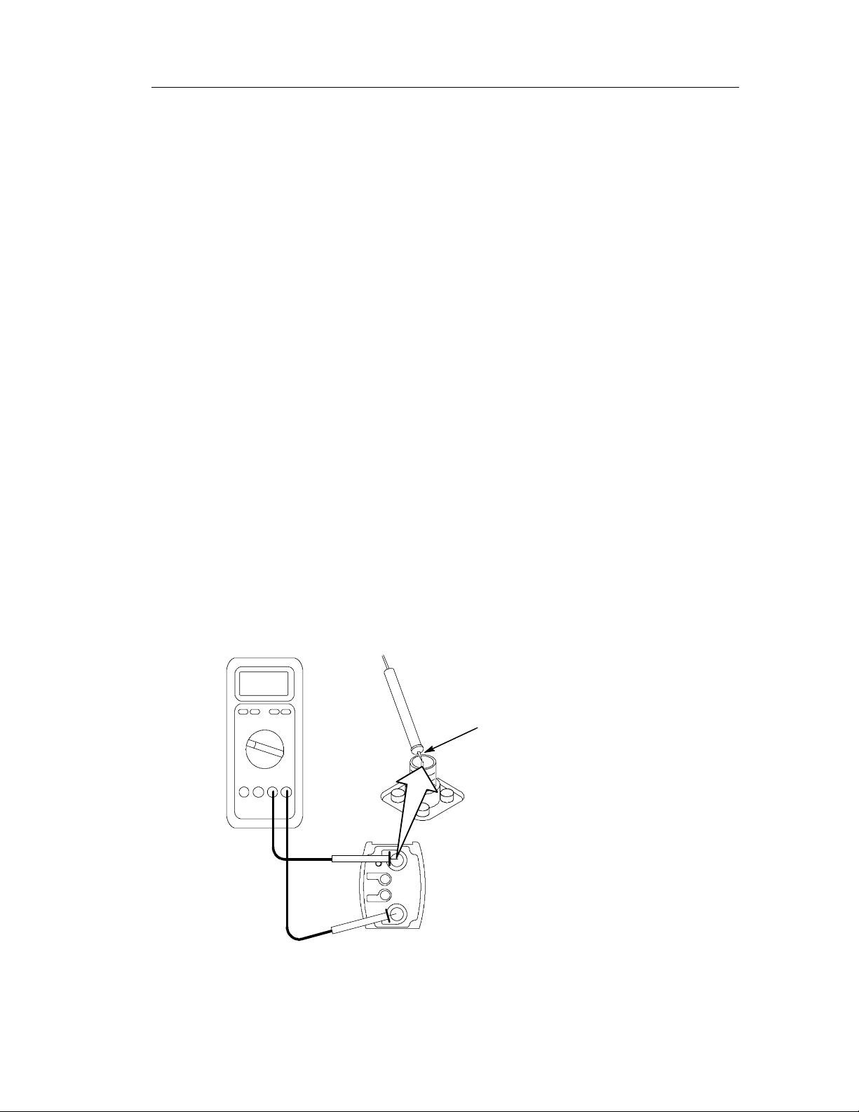
Input Resistance
This test checks the differential mode input resistance—the
resistance between each SMA input. The test is performed with the
probe disconnected from the oscilloscope.
1. Disconnect the probe from the oscilloscope.
2. Remove the SMA terminations from the two probe inputs and
probe the center contacts of the input connectors. See Figure 36.
3. Zero the DMM with its measurement leads connected together on
the lowest scale that can measure 100 Ω.
4. Measure the resistance and write down the value.
5. Reverse the DMM connections and repeat the measurement.
Write down the value.
Appendix B: Performan ce Verification
6. Add the two measurements from steps 4 and 5, and divide the
total by two. Record the result in the test record.
7. Connect the probe to the oscilloscope channel that you will use in
the next test so that the probe warms up to operating temperature.
DMM
Gently touch the center
conductor on each
connector, enough to
get a measurement.
Don’t touch the outer
edge of the connector.
--
+
P7380SMA probe
Figure 36: Checking differential mode input resistance
P7380SMA 8 GHz Differential Probe Instruction Manual
77
Page 94

Appendix B: Performan ce Verification
Termination Voltage Accuracy
These tests compare the termination control voltage that you apply
(using the adjustment control for that termination voltage mode), to
the termination voltage output at the Vterm monitor jacks.
NOTE. The Auto mode LED will flash when the probe inputs are
open-circuit, or below a 50 mV threshold. If the LED continues to
flash after you connect the inputs, cycle the mode SELECT button.
Ext Mode
The Ext mode test setup is shown in Figure 37.
1. Plug the probe directly into an oscilloscope channel and set the
Vterm Source Select to EXT on the probe.
TDS6604 Oscilloscope
DMM (V in)
Step 5
Measure Vterm input voltage at
Black (--)
EXT
Red (+)
External DC input terminals
DMM (V out)
Black (--)
Step 6
Red (+)
Measure Vterm
output voltage
here
50 Ω
terminations
Black (--)
Power supply
+
--
Red (+)
Figure 37: Termination Voltage Accuracy, Ext mode setup
78
P7380SMA 8 GHz Differential Probe Instruction Manual
Page 95

Appendix B: Performan ce Verification
2. Connect the 50 Ω terminations on the three probe SMA
connectors. This sets the common mode input voltage to 0.0 V.
3. The probe attenuation can be set to either 2.5X or 12.5X.
4. Using the 0.080 in pin-to-Banana plug cables, connect the power
supply to the external DC input jacks on the front of the probe.
5. Set the power supply as close as practical to 0.000 volts, using a
DMM to measure this input voltage at the terminals on the front
of the probe. Record this voltage as Vin on the test record.
6. Use the second DMM to measure the output voltage at the
termination voltage monitor jacks on the top of the probe. Record
this voltage as Vout on the test record, and verify that the Vout
voltage is within the specified limits in the min/max columns.
For example, within ±2 mV of the actual Vin voltage that you
measured in the previous step.
7. Repeat steps 5 and 6 for the +2.500 volt and --2.500 volt input
values listed in the test record.
Int Mode
If your oscilloscope supports internal mode, use this test to check the
accuracy of the internally-generated termination voltages. In Int
mode, a graphical user interface in the oscilloscope is used to set the
test values to the 0.000, +2.500 and --2.500 volt levels, instead of
using external power supplies. You do not need to measure these
values in Int mode, as they are digitally set.
See your oscilloscope manual for details on using the interface.
1. Disconnect the power supply from the probe.
2. Set the Vterm Source Select to INT on the probe.
3. Use the graphical user interface in the oscilloscope to set the
termination voltage to 0.000 V.
4. Use the DMM to verify that the termination voltage output at the
Vterm monitor jacks on the top of the probe is within the limits
on the test record. Record this value as Vout on the test record.
5. Repeat steps 3 and 4 for the +2.500 volt and --2.500 volt input
values listed in the test record.
P7380SMA 8 GHz Differential Probe Instruction Manual
79
Page 96

Appendix B: Performan ce Verification
Auto Mode
In Auto mode, the probe measures the input signal DC common
mode voltage and automatically sets the termination voltage to equal
that voltage. In this test, the two signal inputs are connected together
and driven by an external power supply to set the common mode
voltage to the 0.0, +2.500 and --2.500 volt test values.
1. Connect the test setup as shown in Figure 38.
TDS6604 Oscilloscope
P7380SMA
probe
AUTO
DMM (V out)
Black (--)
Red (+)
50 Ω
termination
SMA-to-BNC adapters
--
+
Matched SMA cables
Power supply
-- +
BNC-to-Dual
Banana adapter
DMM (V in)
DMM test leads
BNC cable
B N C F -- t o -- F
adapter
BNC T adapter
Figure 38: Termination Voltage Accuracy, Auto mode setup
2. Set the Vterm Source Select to Auto on the probe.
3. Set the power supply as close as practical to 0.000 volts, using
the DMM to measure this input voltage at the terminals on the
power supply. Record this voltage as Vin on the test record.
80
P7380SMA 8 GHz Differential Probe Instruction Manual
Page 97

Appendix B: Performan ce Verification
4. Use the second DMM to measure the output voltage at the
termination voltage monitor jacks on the top of the probe. Record
this voltage as Vout on the test record, and verify that the Vout
voltage is within the specified limits in the min/max columns.
5. Repeat steps 3 and 4 for the +2.500 volt and --2.500 volt input
values listed in the test record.
P7380SMA 8 GHz Differential Probe Instruction Manual
81
Page 98
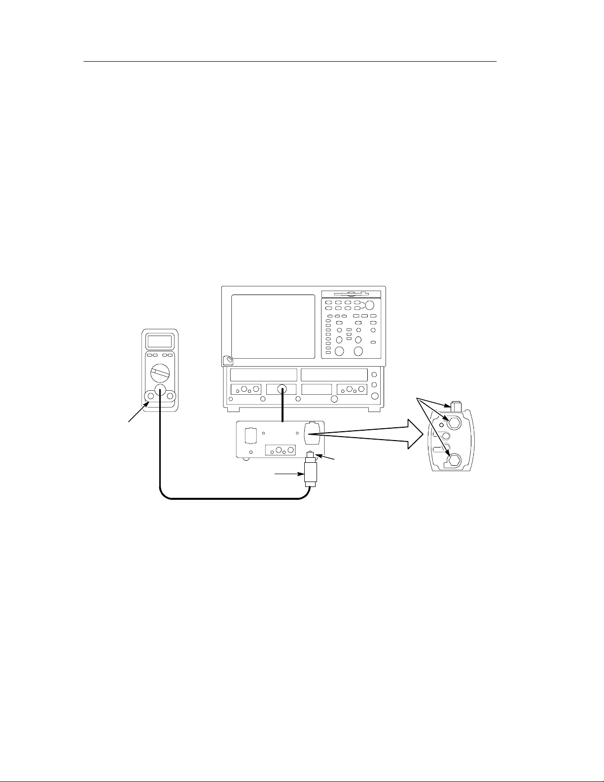
Appendix B: Performan ce Verification
Output Offset Zero
By terminating the two probe SMA inputs with 50 Ω, this procedure
tests the zero output voltage of the probe. The probe output is
measured at the SMA connector on the front of the 80A03 interface.
1. Connect the equipment as shown in Figure 39.
2. Connect two 50 Ω terminations to the two probe SMA inputs on
the probe, and plug the probe into the 80A03 module.
TDS/CSA 8000 Series Oscilloscope
DMM
BNC-to-Dual
Banana adapter
50 Ω Precision
termination
BNC Cable
80A03
Figure 39: Setup for the output offset zero test
3. Set the Vterm source to Ext on the probe. Leave the external
termination control voltage inputs open. This sets the termination
voltage to zero.
4. Set the multimeter to read DC volts.
BNC-SMA
adapter
50 Ω
Terminations
--
+
P7380SMA
probe
82
5. Verify that the output voltage is 0 V,
and 12.5X attenuation settings.
6. Record the results on the test record.
P7380SMA 8 GHz Differential Probe Instruction Manual
±2.5 mV for both the 2.5X
Page 99

DC Gain Accuracy
This test checks the DC gain accuracy of the probe at the two
attenuation settings, 2.5X and 12.5X.
Gain Check at 2.5X Attenuation
1. Set the attenuation on the probe to 2.5X, and the termination
select to Auto.
2. Connect the probe to the power supplies as shown in Figure 40.
Make sure the ground tabs on the BNC-to-dual ba nana plug
adapters are connected to the ground connections on the power
supplies. Monitor the source voltage with one of the DMMs.
TDS/CSA 8000 Series Oscilloscope
Appendix B: Performan ce Verification
DMM
(V out)
BNC
Cable
Banana adapter
BNC-SMA
adapter
50 Ω Precision
termination
BNC-to-Dual
80A03
P7380SMA probe
Power supply
-- +
--
+
DMM (V in)
-- +
BNC-to-Dual
Banana adapter
BNC-to-SMA adapter
Matched SMA cables
(+)(--)
Power supply
-- +
Figure 40: DC Gain Accuracy setup
P7380SMA 8 GHz Differential Probe Instruction Manual
83
Page 100

Appendix B: Performan ce Verification
3. Set the voltage on each power supply to approximately +0.125 V
(+0.25 V differential total). This repre sents 80% of the probe
dynamic range in this attenuation setting. Record this source
voltage as V
1.
in
4. Record the output voltage (on the second DMM) as V
out
1.
5. Disconnect the BNC-to-dual banana plug adapters from the
power supplies. Leave the DMM leads connected to the adapters.
6. Connect the BNC-to-dual banana plug adapters into the opposite
power supplies to reverse the voltage polarity t o the probe inputs.
See Figure 41.
7. Record the actual source voltage (now a negative value), as V
DMM
(--)
Power supply
+--
(+)
Power supply
in
2.
BNC-to-Dual
BNC-to-Dual
Banana adapter
Banana adapter
BNC-to-SMA
84
-- +-- +
BNC-to-Dual
adapter
--
SMA cable
+
SMA cable
Banana adapter
BNC-to-SMA
adapter
Figure 41: Reverse the power supply polarity on the probe inputs
8. Record the output voltage (on the second DMM) as V
9. Calculate the gain as follows: (V
1--V
out
2) ÷ (Vin1--Vin2).
out
out
2.
P7380SMA 8 GHz Differential Probe Instruction Manual
 Loading...